78M6618 PDU1 Hardware Design Guidelines
30
AVAILABLE 78M6618 PDU1 Hardware Design Guidelines APPLICATION NOTE AN_6618_027 April 2012 Rev. 3 1 1 Introduction Several applications and markets utilize intelligent Power Distribution Units (PDUs) or power strips for power monitoring and on/off control of data center equipment, workstations, home entertainment systems, or sub panel circuits. The PDU1 solution for the 78M6618 energy measurement System-on- Chip (SoC) is designed for single-phase systems with measurement on a per outlet or circuit level. This application note provides hardware and system design guidelines for those implementing the 78M6618 PDU1 solution in their products. These guidelines aim to reduce design cycle times by reviewing the challenges and solutions to achieve minimum crosstalk and greatest accuracy in a multiple-outlet power strip. This application note starts out describing generic recommendations common to all applications. Then it provides design examples and relevant tips for different implementations of a PDU design. These examples refer to available evaluation boards whose design files are available for download. Figure 1: Typical Power Distribution Units
Transcript of 78M6618 PDU1 Hardware Design Guidelines

AVAILABLE
78M6618 PDU1 Hardware Design Guidelines
APPLICATION NOTE AN_6618_027 April 2012
Rev. 3 1
1 Introduction Several applications and markets utilize intelligent Power Distribution Units (PDUs) or power strips for power monitoring and on/off control of data center equipment, workstations, home entertainment systems, or sub panel circuits. The PDU1 solution for the 78M6618 energy measurement System-on-Chip (SoC) is designed for single-phase systems with measurement on a per outlet or circuit level. This application note provides hardware and system design guidelines for those implementing the 78M6618 PDU1 solution in their products. These guidelines aim to reduce design cycle times by reviewing the challenges and solutions to achieve minimum crosstalk and greatest accuracy in a multiple-outlet power strip. This application note starts out describing generic recommendations common to all applications. Then it provides design examples and relevant tips for different implementations of a PDU design. These examples refer to available evaluation boards whose design files are available for download.
Figure 1: Typical Power Distribution Units
78M6618 PDU1 Hardware Design Guidelines AN_6618_027
2 Rev 3
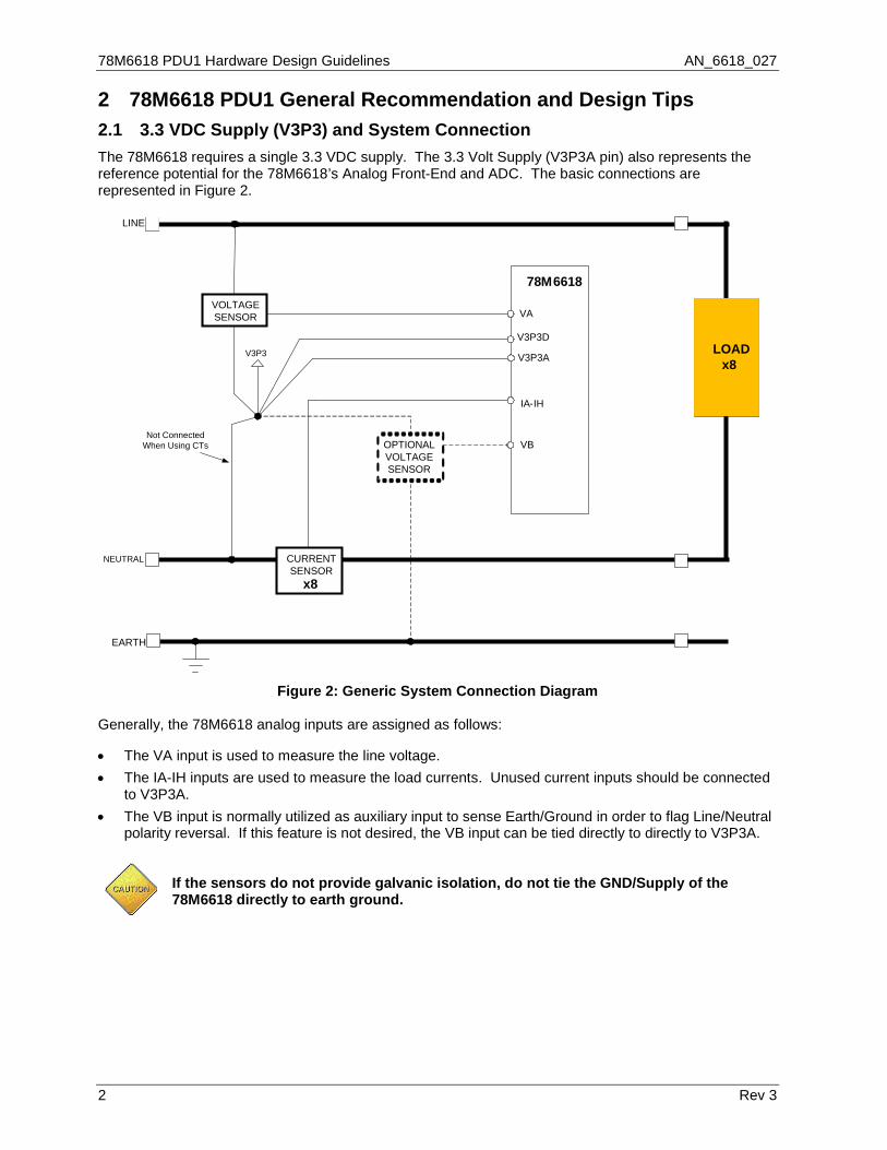
2 78M6618 PDU1 General Recommendation and Design Tips 2.1 3.3 VDC Supply (V3P3) and System Connection The 78M6618 requires a single 3.3 VDC supply. The 3.3 Volt Supply (V3P3A pin) also represents the reference potential for the 78M6618’s Analog Front-End and ADC. The basic connections are represented in Figure 2.
LINE
VA
VB
IA-IH
78M6618VOLTAGESENSOR
OPTIONAL VOLTAGESENSOR
CURRENTSENSOR
V3P3AV3P3
V3P3D
x8LOAD
EARTH
NEUTRAL
x8
Not Connected When Using CTs
Figure 2: Generic System Connection Diagram
Generally, the 78M6618 analog inputs are assigned as follows: • The VA input is used to measure the line voltage. • The IA-IH inputs are used to measure the load currents. Unused current inputs should be connected
to V3P3A. • The VB input is normally utilized as auxiliary input to sense Earth/Ground in order to flag Line/Neutral
polarity reversal. If this feature is not desired, the VB input can be tied directly to directly to V3P3A.
If the sensors do not provide galvanic isolation, do not tie the GND/Supply of the 78M6618 directly to earth ground.
AN_6618_027 78M6618 PDU1 Hardware Design Guidelines
Rev. 3 3
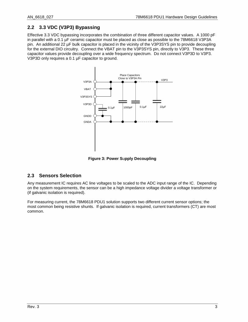
2.2 3.3 VDC (V3P3) Bypassing Effective 3.3 VDC bypassing incorporates the combination of three different capacitor values. A 1000 pF in parallel with a 0.1 µF ceramic capacitor must be placed as close as possible to the 78M6618 V3P3A pin. An additional 22 µF bulk capacitor is placed in the vicinity of the V3P3SYS pin to provide decoupling for the external DIO circuitry. Connect the VBAT pin to the V3P3SYS pin, directly to V3P3. These three capacitor values provide decoupling over a wide frequency spectrum. Do not connect V3P3D to V3P3. V3P3D only requires a 0.1 µF capacitor to ground.
GNDA
V3P3SYS
VBAT
V3P3A
GNDD
1000pF 0.1μF 22μF
V3P3
Place Capacitors Close to V3P3A Pin
V3P3D0.1μF
Figure 3: Power Supply Decoupling
2.3 Sensors Selection Any measurement IC requires AC line voltages to be scaled to the ADC input range of the IC. Depending on the system requirements, the sensor can be a high impedance voltage divider a voltage transformer or (if galvanic isolation is required). For measuring current, the 78M6618 PDU1 solution supports two different current sensor options; the most common being resistive shunts. If galvanic isolation is required, current transformers (CT) are most common.
78M6618 PDU1 Hardware Design Guidelines AN_6618_027
4 Rev 3
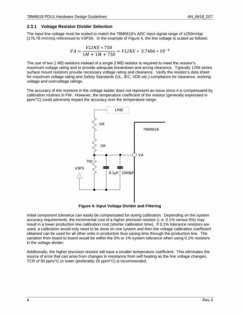
2.3.1 Voltage Resistor Divider Selection The input line voltage must be scaled to match the 78M6618’s ADC input signal range of ±250mVpp (176.78 mVrms) referenced to V3P3A. In the example of Figure 4, the line voltage is scaled as follows:
𝑉𝐴 =𝑉𝐿𝐼𝑁𝐸 ∗ 750
1𝑀 + 1𝑀 + 750= 𝑉𝐿𝐼𝑁𝐸 ∗ 3.7486 ∗ 10−4
The use of two 1 MΩ resistors instead of a single 2 MΩ resistor is required to meet the resistor’s maximum voltage rating and to provide adequate breakdown and arcing clearance. Typically 1206 series surface mount resistors provide necessary voltage rating and clearance. Verify the resistor’s data sheet for maximum voltage rating and Safety Standards (UL, IEC, VDE etc.) compliance for clearance, working voltage and overvoltage ratings. The accuracy of the resistors in the voltage ladder does not represent an issue since it is compensated by calibration routines in FW. However, the temperature coefficient of the resistor (generally expressed in ppm/°C) could adversely impact the accuracy over the temperature range.
VA
1M
1M
750
LINE
V3P31000pF0.1µF
78M6618
Figure 4: Input Voltage Divider and Filtering
Initial component tolerance can easily be compensated for during calibration. Depending on the system accuracy requirements, the incremental cost of a higher precision resistor (i. e. 0.1% versus 5%) may result in a lower production line calibration cost (shorter calibration time). If 0.1% tolerance resistors are used, a calibration would only need to be done on one system and then the voltage calibration coefficient obtained can be used for all other units in production thus saving time through the production line. The variation from board to board would be within the 5% or 1% system tolerance when using 0.1% resistors in the voltage divider. Additionally, the higher precision resistor will have a smaller temperature coefficient. This eliminates the source of error that can arise from changes in resistance from self heating as the line voltage changes. TCR of 50 ppm/°C or lower (preferably 25 ppm/°C) is recommended.
AN_6618_027 78M6618 PDU1 Hardware Design Guidelines
Rev. 3 5
2.3.2 Voltage Transformers The voltage measurement circuit described in Section 2.3.1 can be replaced with a voltage transformer (VT). The VT replaces the two 2 MΩ resistor divider networks and requires use of only VA. Use of a CT (for current sensing) with a VT provides complete galvanic isolation from the plant wiring. A good quality VT provides accurate linear measurements from 100VAC to 240VAC. The VT is typically a 1:1 ratio transformer with a current rating of < 10 mA. The current limiting resistors should be chosen to keep the primary current below the transformer rating at the design line voltage. For example, if the VT primary is rated at 2 mA and the design line voltage is 240VRMS, the RMS current in the primary will be: 2 mA ≥ 240 V/2*Rcurrent limiting That requires that Rcurrent limiting ≥ 60 KΩ. Setting Rcurrent limiting ≥ 75 KΩ would limit the current to 1.6 mA and would provide 25% headroom for over voltages. The burden resistor for the VT should be set so that RBURDEN* IPEAK SECONDARY ≤ 250 mV. Assuming that the voltage waveform is sinusoidal, the current waveform in the VT will also be sinusoidal, the peak current for 2 mA RMS would be 2*√2 mA, or 2 .818 mA. The VT burden resistor should then be RBURDEN ≤ 250 mV/2.818 mA, or RBURDEN ≤ 88Ω., so selecting a convenient value for RBURDEN between 75Ω and 86.6Ω should give good results. Good quality VTs introduce minimal phase shift between the primary to secondary winding. Phase compensation parameters are available to compensate for any phase delays between voltage and current samples.
78M6618 PDU1 Hardware Design Guidelines AN_6618_027
6 Rev 3
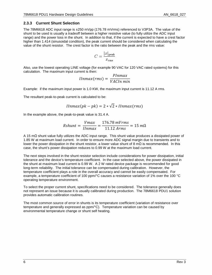
2.3.3 Current Shunt Selection The 78M6618 ADC input range is ±250 mVpp (176.78 mVrms) referenced to V3P3A. The value of the shunt to be used is usually a tradeoff between a higher resistive value (to fully utilize the ADC input range) and the power loss in the shunt. In addition to that, if the current is expected to have a crest factor higher than 1.414 (sinusoidal condition), the peak current should be considered when calculating the value of the shunt resistor. The crest factor is the ratio between the peak and the rms value:
Also, use the lowest operating LINE voltage (for example 90 VAC for 120 VAC rated systems) for this calculation. The maximum input current is then:
𝐼𝐼𝑛𝑚𝑎𝑥(𝑟𝑚𝑠) = 𝑃𝐼𝑛𝑚𝑎𝑥
𝑉𝐴𝐶𝐼𝑛 𝑚𝑖𝑛
Example: if the maximum input power is 1.0 KW, the maximum input current is 11.12 A rms. The resultant peak-to-peak current is calculated to be:
𝐼𝐼𝑛𝑚𝑎𝑥(𝑝𝑘 − 𝑝𝑘) = 2 ∗ √2 ∗ 𝐼𝐼𝑛𝑚𝑎𝑥(𝑟𝑚𝑠) In the example above, the peak-to-peak value is 31.4 A.
𝑅𝑠ℎ𝑢𝑛𝑡 = 𝑉𝑚𝑎𝑥𝐼𝐼𝑛𝑚𝑎𝑥
=176.78 𝑚𝑉𝑟𝑚𝑠
11.12 𝐴𝑟𝑚𝑠= 15 𝑚Ω
A 15 mΩ shunt value fully utilizes the ADC input range. This shunt value produces a dissipated power of 1.85 W at maximum load current. In order to ensure more ADC signal margin due to transients and to lower the power dissipation in the shunt resistor, a lower value shunt of 8 mΩ is recommended. In this case, the shunt’s power dissipation reduces to 0.99 W at the maximum load current. The next steps involved in the shunt resistor selection include considerations for power dissipation, initial tolerance and the device’s temperature coefficient. In the case selected above, the power dissipated in the shunt at maximum load current is 0.99 W. A 2 W rated device package is recommended for good long-term reliability. The initial tolerance can be compensated during calibration. However, the temperature coefficient plays a role in the overall accuracy and cannot be easily compensated. For example, a temperature coefficient of 100 ppm/°C causes a resistance variation of 1% over the 100 °C operating temperature environment. To select the proper current shunt, specifications need to be considered. The tolerance generally does not represent an issue because it is usually calibrated during production. The 78M6618 PDU1 solution provides automatic calibration routines. The most common source of error in shunts is its temperature coefficient (variation of resistance over temperature and generally expressed as ppm/°C). Temperature variation can be caused by environmental temperature change or shunt self heating.

AN_6618_027 78M6618 PDU1 Hardware Design Guidelines
Rev. 3 7
2.3.4 Current Transformers The selection of a current transformer with respect for the desired measurement accuracy includes factors such as line frequency, measured current range and the CT’s turns ratio. Also, subjecting a current transformer to load currents above the manufacturer’s rated current specification may saturate the CT and cause winding failures due to excessive temperature rise. On the other hand, a current transformer that is rated much higher than the target load current might be restrictively too large and expensive for its purpose.
Figure 5: Current Transformer (CT) Basic Connections
Usually, current transformers have turns ratios ranging from 10:1 to 2500:1. The higher the turns ratio (TurnRatio = Nsecondary/Nprimary), the higher the resolution of the current measurement. A too high turns ratio increases distributed capacitance and leakage inductance. These characteristics may decrease the CT’s accuracy and capability to operate at higher frequencies. However, if the number of turns is too low, the output signal may distort or “droop” (for positively sloped unipolar input signals). Such distortion may cause measurement inaccuracies. We recommend a minimum turns ratio of 1000:1. The next step towards selecting a current transformer is the calculation of the burden resistor’s value (RBurden). The 78M6618 signal input range is 176.78 mVrms (±250 mVpk). Therefore, the CT’s secondary output voltage (Vout) must operate within this range. Assuming the maximum load current is 20 Arms (28.284A pk), a 1000:1 ratio current transformer will produce a secondary current of 20 mA rms (28.284 mA pk). Per Figure 5, the burden resistor’s value is calculated as follows:
𝑅𝐵𝑢𝑟𝑑𝑒𝑛 = 𝑉𝑜𝑢𝑡𝐼𝑜𝑢𝑡
Using the values in the above example, the value of the burden resistor is:
𝑅𝐵𝑢𝑟𝑑𝑒𝑛 = 0.250
0.028284= 8.85 Ω
A standard value 8.2 Ω resistor is recommended.
78M6618 PDU1 Hardware Design Guidelines AN_6618_027
8 Rev 3
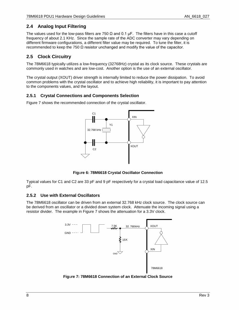
2.4 Analog Input Filtering The values used for the low-pass filters are 750 Ω and 0.1 µF. The filters have in this case a cutoff frequency of about 2.1 KHz. Since the sample rate of the ADC converter may vary depending on different firmware configurations, a different filter value may be required. To tune the filter, it is recommended to keep the 750 Ω resistor unchanged and modify the value of the capacitor. 2.5 Clock Circuitry The 78M6618 typically utilizes a low-frequency (32768Hz) crystal as its clock source. These crystals are commonly used in watches and are low-cost. Another option is the use of an external oscillator. The crystal output (XOUT) driver strength is internally limited to reduce the power dissipation. To avoid common problems with the crystal oscillator and to achieve high reliability, it is important to pay attention to the components values, and the layout. 2.5.1 Crystal Connections and Components Selection Figure 7 shows the recommended connection of the crystal oscillator.
XIN
XOUT
C1
C2
32.768 kHz
Y1
Figure 6: 78M6618 Crystal Oscillator Connection Typical values for C1 and C2 are 33 pF and 9 pF respectively for a crystal load capacitance value of 12.5 pF. 2.5.2 Use with External Oscillators The 78M6618 oscillator can be driven from an external 32.768 kHz clock source. The clock source can be derived from an oscillator or a divided down system clock. Attenuate the incoming signal using a resistor divider. The example in Figure 7 shows the attenuation for a 3.3V clock.
XIN
XOUT32. 768 kHz
15
K7.5
K
GND
3.3V
GND
78M6618
Figure 7: 78M6618 Connection of an External Clock Source

AN_6618_027 78M6618 PDU1 Hardware Design Guidelines
Rev. 3 9
2.5.3 Component Placement and Layout To minimize noise sensitivity to spurious coupling or parasitic antenna phenomena on the PCB, the connections of the crystal to oscillator input and output and to other components must be as short as possible. The best practice is to place the crystal and phasing capacitors as close as possible to the 78M6618. This helps to minimize the length of the connections. The currents flowing through the two load capacitors (C1 and C2) are in opposition. The best practice is to connect the two capacitors before connecting to the ground reference. At that time, the current back to the ground is significantly reduced. The connections must be as short as possible and of identical lengths. Avoid long connections from these capacitors that make a large loop on the PCB, which behaves like an antenna and can collect surrounding high-frequency radiation. The reference ground of the oscillator must be as quiet as possible; otherwise, high-frequency noise is transmitted directly to the oscillator input and output, resulting in degradation of the oscillator performance. To prevent cross-coupling to fast signals with high-level harmonic content, do not route signal traces through the crystal area. Both oscillator pin connections are critical. Do not locate power magnetic components near the crystal oscillator components. Select a PCB layout topology that places the crystal components on the opposite PCB side from the power magnetic components and resulting magnetic fields. Vias in the oscillator circuit should only be used for connections to the ground plane. Do not share ground connections; instead, make a separate connection to ground for each component that requires grounding. If possible, place multiple vias in parallel for each connection to the ground plane. The use of high-quality components in the oscillator circuit is equally important to achieve correct and reliable operation. Capacitors should be high-quality capacitors with very low ESR, designed for use in high-frequency applications (i.e., NP0 and COG). Figure 8 shows a layout example for the crystal oscillator.
Y1 CRYSTAL BOTTOM VIEW
1
GNDAV3P3A
GNDD
17
18
34
35
51
68
GNDD V3P3D
Figure 8: Crystal Y1 and Capacitors C7/C9 In this case, the placement and layout of the crystal oscillator components are on the same side of the PCB with the integrated circuit. There is a ground guard-ring surrounding the crystal oscillator. One way to accomplish this is by surrounding the circuit with a wide grounded trace. For this to work, the grounded trace must have zero current flowing through it. In this example, there is a “floating ground” with no connections other than the oscillator’s GND.
78M6618 PDU1 Hardware Design Guidelines AN_6618_027
10 Rev 3
2.5.4 Troubleshooting Oscillator Circuitry A common cause of crystal oscillator malfunction is the buildup of contaminants on the PCB. PCB contaminants such as flux, humidity, finger prints, etc. can create a high-impedance path from one of the oscillator pins to GND or the V3P3 supply preventing oscillator startup. To overcome this problem, check for contaminant accumulation between the crystal leads and beneath the 78M6618 package. Board cleanliness is most critical when using water soluble solder paste. 2.5.5 Soldering Process An inappropriate soldering profile can cause excessive stress on the components. Improper handling of the crystal may cause the fracture of the hermetic seal. This would allow moisture and other contaminants to infiltrate the case, causing sporadic operation or complete failure. Excessive temperatures or excessive exposure time to high temperatures due to an inappropriate soldering profile can also damage the crystal. 2.5.6 Oscillator Start-up Time In general, the startup time for a low-frequency crystal oscillator is longer than a high-frequency crystal. For a 32.768 kHz crystal, startup should be within the range of 200 ms to 400 ms. Startup time exceeding 700 milliseconds is most likely an indicator that the crystal is having trouble starting at all, and that the value chosen for the capacitors C1 and C2 does not meet the crystal manufacturer’s requirements or there are other causes such as contaminants (solder flux etc.). Crystals require a certain amount of power to start into a stable oscillation pattern. Since the power supplied to the crystal is going to be a function of the power supply, oscillator start-up times are going to be strongly affected by the rise time of the power supply. Another factor is that a power supply with very sharp rise times will act like an impulse to the crystal, causing it to start faster when compared to using a power supply with a very slow rise time. Some crystal characteristics that affect startup time: • High Q-factor crystal oscillators typically start slower than crystal oscillators with higher frequency
tolerance. • Crystal with low load capacitance typically start faster than crystals requiring high load capacitance. • Crystals with low ESR start more quickly than high ESR crystals. • Oscillators with high OA (Oscillation Allowance) start faster than low OA crystal oscillators. 2.5.7 Minimizing Voltage and Temperature Effects The crystal oscillator should be tested over the entire temperature and voltage range in which it is expected to operate. The most critical corner is at the highest temperature and lowest supply voltage. This condition leads to minimum loop gain and could result in a slow or no start-up. To minimize undesirable temperature effects, use capacitors with a low temperature coefficient, such as NP0 or COG types. Verify that all components are specified to work for the entire temperature and voltage range, the crystal in particular. 2.6 QFN Substrate Pad The 78M6618 device comes in a QFN-68 package, which has a large substrate PCB pad on the bottom side. Since the power dissipation of the device is minimal, the PCB pad is not required for heat dissipation. The PCB pad can be left floating or connected to GND. The PCB pad can have reduced dimensions (up to 50% of the package pad dimension) in order to minimize flux residue under the device and to reduce solder shorts due to excessive solder paste from a large pad surface.
AN_6618_027 78M6618 PDU1 Hardware Design Guidelines
Rev. 3 11
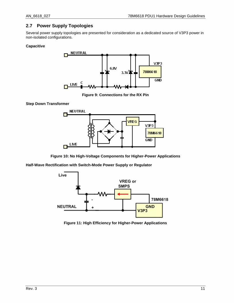
2.7 Power Supply Topologies Several power supply topologies are presented for consideration as a dedicated source of V3P3 power in non-isolated configurations. Capacitive
Figure 9: Connections for the RX Pin Step Down Transformer
Figure 10: No High-Voltage Components for Higher-Power Applications Half-Wave Rectification with Switch-Mode Power Supply or Regulator
Figure 11: High Efficiency for Higher-Power Applications
78M6618 PDU1 Hardware Design Guidelines AN_6618_027
12 Rev 3
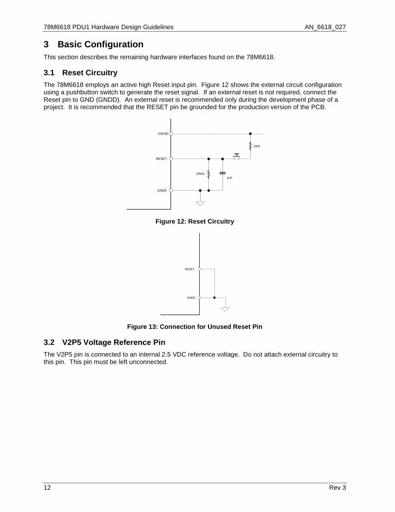
3 Basic Configuration This section describes the remaining hardware interfaces found on the 78M6618. 3.1 Reset Circuitry The 78M6618 employs an active high Reset input pin. Figure 12 shows the external circuit configuration using a pushbutton switch to generate the reset signal. If an external reset is not required, connect the Reset pin to GND (GNDD). An external reset is recommended only during the development phase of a project. It is recommended that the RESET pin be grounded for the production version of the PCB.
GNDD
V3P3D
RESET
1nF10KΩ
1KΩ
Figure 12: Reset Circuitry
GNDD
RESET
Figure 13: Connection for Unused Reset Pin 3.2 V2P5 Voltage Reference Pin The V2P5 pin is connected to an internal 2.5 VDC reference voltage. Do not attach external circuitry to this pin. This pin must be left unconnected.

AN_6618_027 78M6618 PDU1 Hardware Design Guidelines
Rev. 3 13
V3P3
V3P3 -400mV
V3P3 - 10mV
VBIAS
0V
Battery orresetmode
Normaloperation,
WDTenabled
WDT dis-abled
V1
3.3 V1 Pin The V1 pin is connected to an internal power-fail comparator. The V1 input voltage is compared to an internal reference voltage of 1.6 V (VBIAS). If the V1 voltage is above VBIAS, the comparator output is high (1) signaling normal operation. If the V1 voltage is below VBIAS, the comparator output is low (0) signaling battery mode operation (via an external battery attached to the VBAT pin). Connect the voltage divider shown in Figure 15 to the V1 pin to enable normal (WDT enabled) 78M6618 operation. The watchdog may be disabled for debugging by raising the V1 pin above 2.9 V.
Figure 14: V1 Detector Voltage Thresholds R3 is used to provide hysteresis to the comparator. The input pin V1 sinks 1 µA when V1< VBIAS and 0 µA when V1 ≥ VBIAS. Therefore the thresholds are:
𝑉3𝑃3 ≤ 𝑅1+𝑅2𝑅2
𝑉𝐵𝐼𝐴𝑆 (High to Low transition, VBIAS = 1.6 VDC)
𝑉3𝑃3 > 𝑅1+𝑅2𝑅2
(𝑉𝐵𝐼𝐴𝑆 + 𝑅3 ∗ 1𝐸 − 6𝐴) (Low to High transition, VBIAS = 1.6 VDC) C1 provides additional filtering to the V1 input to prevent spurious commutations of the V1 comparator.
Figure 15: Voltage Divider for V1
2kΩ
78M6618 PDU1 Hardware Design Guidelines AN_6618_027
14 Rev 3
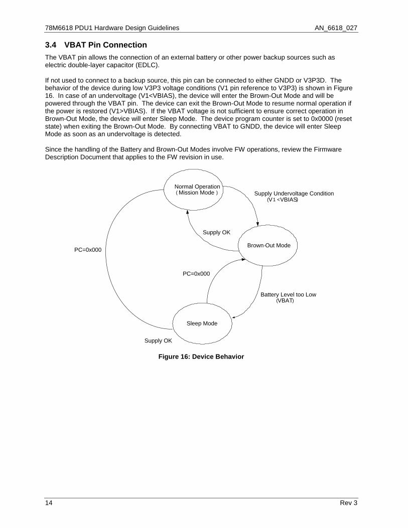
3.4 VBAT Pin Connection The VBAT pin allows the connection of an external battery or other power backup sources such as electric double-layer capacitor (EDLC). If not used to connect to a backup source, this pin can be connected to either GNDD or V3P3D. The behavior of the device during low V3P3 voltage conditions (V1 pin reference to V3P3) is shown in Figure 16. In case of an undervoltage (V1<VBIAS), the device will enter the Brown-Out Mode and will be powered through the VBAT pin. The device can exit the Brown-Out Mode to resume normal operation if the power is restored (V1>VBIAS). If the VBAT voltage is not sufficient to ensure correct operation in Brown-Out Mode, the device will enter Sleep Mode. The device program counter is set to 0x0000 (reset state) when exiting the Brown-Out Mode. By connecting VBAT to GNDD, the device will enter Sleep Mode as soon as an undervoltage is detected. Since the handling of the Battery and Brown-Out Modes involve FW operations, review the Firmware Description Document that applies to the FW revision in use.
Normal Operation( Mission Mode )
Brown-Out Mode
(V1 < VBIAS)Supply Undervoltage Condition
Supply OK
Sleep Mode
Battery Level too Low(VBAT)
Supply OK
PC=0x000
PC=0x000
Figure 16: Device Behavior
AN_6618_027 78M6618 PDU1 Hardware Design Guidelines
Rev. 3 15
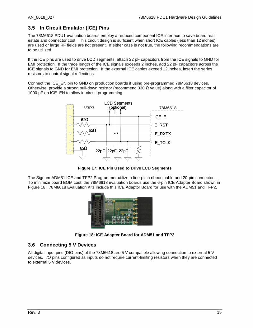
3.5 In Circuit Emulator (ICE) Pins The 78M6618 PDU1 evaluation boards employ a reduced component ICE interface to save board real estate and connector cost. This circuit design is sufficient when short ICE cables (less than 12 inches) are used or large RF fields are not present. If either case is not true, the following recommendations are to be utilized. If the ICE pins are used to drive LCD segments, attach 22 pF capacitors from the ICE signals to GND for EMI protection. If the trace length of the ICE signals exceeds 2 inches, add 22 pF capacitors across the ICE signals to GND for EMI protection. If the external ICE cables exceed 12 inches, insert the series resistors to control signal reflections. Connect the ICE_EN pin to GND on production boards if using pre-programmed 78M6618 devices. Otherwise, provide a strong pull-down resistor (recommend 330 Ω value) along with a filter capacitor of 1000 pF on ICE_EN to allow in-circuit programming.
Figure 17: ICE Pin Used to Drive LCD Segments The Signum ADM51 ICE and TFP2 Programmer utilize a fine-pitch ribbon cable and 20-pin connector. To minimize board BOM cost, the 78M6618 evaluation boards use the 6-pin ICE Adapter Board shown in Figure 18. 78M6618 Evaluation Kits include this ICE Adaptor Board for use with the ADM51 and TFP2.
Figure 18: ICE Adapter Board for ADM51 and TFP2 3.6 Connecting 5 V Devices All digital input pins (DIO pins) of the 78M6618 are 5 V compatible allowing connection to external 5 V devices. I/O pins configured as inputs do not require current-limiting resistors when they are connected to external 5 V devices.
E_RST
E_RXTX
E_TCLK
62 Ω
62 Ω
62 Ω
22pF 22pF 22pF
LCD Segments (optional)
ICE_E
E_RST
78M6618
E_RXTX
E_TCLK
62 Ω
62 Ω
62 Ω
22pF 22pF 22pF
LCD Segments (optional)
ICE_E
V3P3
78M6618 PDU1 Hardware Design Guidelines AN_6618_027
16 Rev 3
3.7 Driving External Loads Connect external loads to the digital outputs (DIO pins) as shown in Figure 19
V3P3
DGND
V3P3
DGND
NOT RECOMMENDED RECOMMENDED Figure 19: Connecting an External Load to a Digital Output
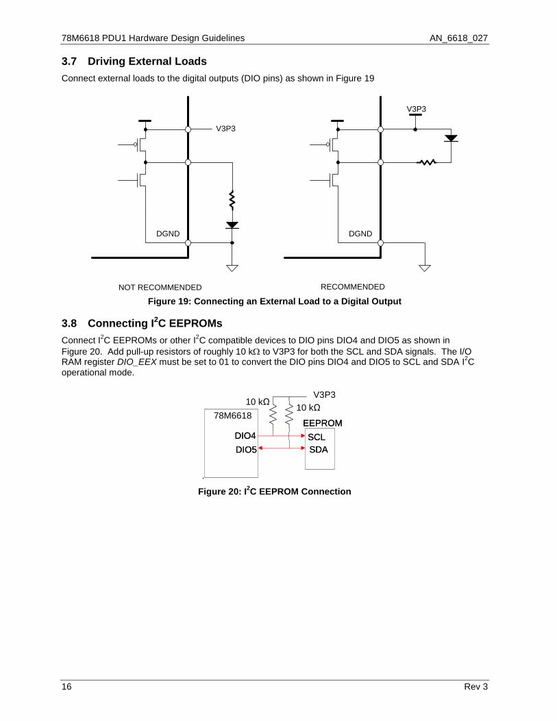
3.8 Connecting I2C EEPROMs Connect I2C EEPROMs or other I2C compatible devices to DIO pins DIO4 and DIO5 as shown in Figure 20. Add pull-up resistors of roughly 10 kΩ to V3P3 for both the SCL and SDA signals. The I/O RAM register DIO_EEX must be set to 01 to convert the DIO pins DIO4 and DIO5 to SCL and SDA I2C operational mode.
.
Figure 20: I2C EEPROM Connection
DIO4 DIO5
78M6618 EEPROM SCL SDA
V3P3 10 kΩ 10 kΩ
DIO4 DIO5
EEPROM SCL SDA
AN_6618_027 78M6618 PDU1 Hardware Design Guidelines
Rev. 3 17
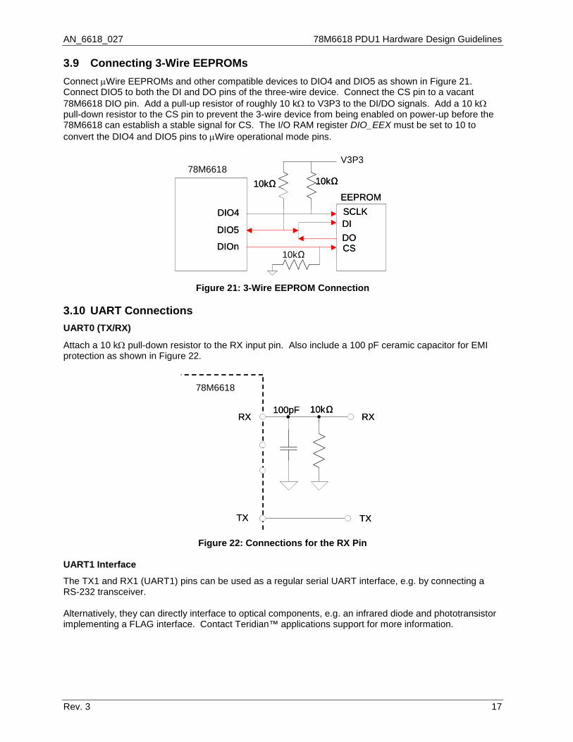
3.9 Connecting 3-Wire EEPROMs Connect µWire EEPROMs and other compatible devices to DIO4 and DIO5 as shown in Figure 21. Connect DIO5 to both the DI and DO pins of the three-wire device. Connect the CS pin to a vacant 78M6618 DIO pin. Add a pull-up resistor of roughly 10 kΩ to V3P3 to the DI/DO signals. Add a 10 kΩ pull-down resistor to the CS pin to prevent the 3-wire device from being enabled on power-up before the 78M6618 can establish a stable signal for CS. The I/O RAM register DIO_EEX must be set to 10 to convert the DIO4 and DIO5 pins to µWire operational mode pins.
Figure 21: 3-Wire EEPROM Connection
3.10 UART Connections UART0 (TX/RX)
Attach a 10 kΩ pull-down resistor to the RX input pin. Also include a 100 pF ceramic capacitor for EMI protection as shown in Figure 22.
Figure 22: Connections for the RX Pin
UART1 Interface
The TX1 and RX1 (UART1) pins can be used as a regular serial UART interface, e.g. by connecting a RS-232 transceiver. Alternatively, they can directly interface to optical components, e.g. an infrared diode and phototransistor implementing a FLAG interface. Contact Teridian™ applications support for more information.
TX
RX 10k Ω 100pF
RX
TX TX
RX
78M6618
10k Ω 100pF RX
TX
DIO4
DIO5
EEPROM SCLK DI
10k Ω
CS DIOn DO
10k Ω
DIO4
DIO5
78M6618
EEPROM SCLK DI
V3P3
10k Ω
CS DIOn DO
10k Ω
10k Ω
78M6618 PDU1 Hardware Design Guidelines AN_6618_027
18 Rev 3
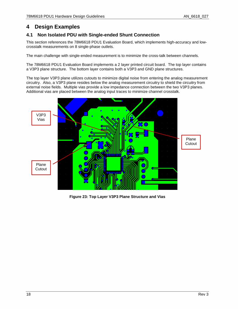
4 Design Examples 4.1 Non Isolated PDU with Single-ended Shunt Connection This section references the 78M6618 PDU1 Evaluation Board, which implements high-accuracy and low-crosstalk measurements on 8 single-phase outlets. The main challenge with single-ended measurement is to minimize the cross-talk between channels. The 78M6618 PDU1 Evaluation Board implements a 2 layer printed circuit board. The top layer contains a V3P3 plane structure. The bottom layer contains both a V3P3 and GND plane structures. The top layer V3P3 plane utilizes cutouts to minimize digital noise from entering the analog measurement circuitry. Also, a V3P3 plane resides below the analog measurement circuitry to shield the circuitry from external noise fields. Multiple vias provide a low impedance connection between the two V3P3 planes. Additional vias are placed between the analog input traces to minimize channel crosstalk.
Figure 23: Top Layer V3P3 Plane Structure and Vias
Plane Cutout
Plane Cutout
V3P3 Vias
AN_6618_027 78M6618 PDU1 Hardware Design Guidelines
Rev. 3 19
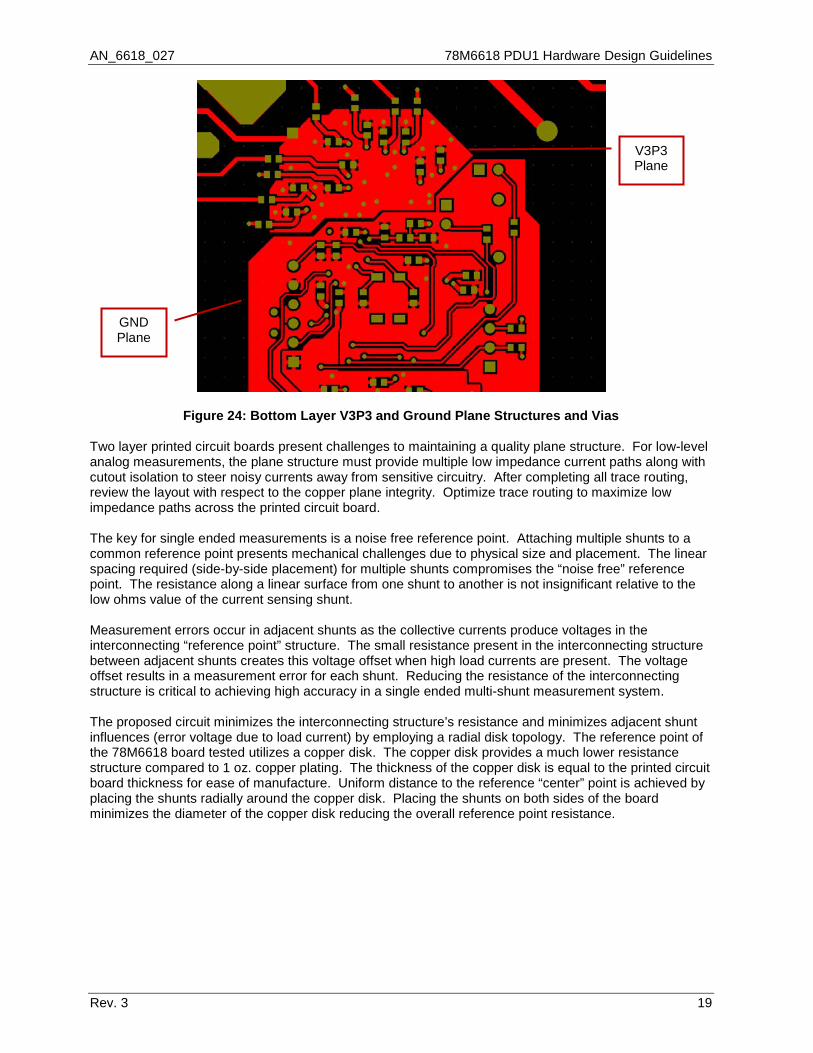
Figure 24: Bottom Layer V3P3 and Ground Plane Structures and Vias
Two layer printed circuit boards present challenges to maintaining a quality plane structure. For low-level analog measurements, the plane structure must provide multiple low impedance current paths along with cutout isolation to steer noisy currents away from sensitive circuitry. After completing all trace routing, review the layout with respect to the copper plane integrity. Optimize trace routing to maximize low impedance paths across the printed circuit board. The key for single ended measurements is a noise free reference point. Attaching multiple shunts to a common reference point presents mechanical challenges due to physical size and placement. The linear spacing required (side-by-side placement) for multiple shunts compromises the “noise free” reference point. The resistance along a linear surface from one shunt to another is not insignificant relative to the low ohms value of the current sensing shunt. Measurement errors occur in adjacent shunts as the collective currents produce voltages in the interconnecting “reference point” structure. The small resistance present in the interconnecting structure between adjacent shunts creates this voltage offset when high load currents are present. The voltage offset results in a measurement error for each shunt. Reducing the resistance of the interconnecting structure is critical to achieving high accuracy in a single ended multi-shunt measurement system. The proposed circuit minimizes the interconnecting structure’s resistance and minimizes adjacent shunt influences (error voltage due to load current) by employing a radial disk topology. The reference point of the 78M6618 board tested utilizes a copper disk. The copper disk provides a much lower resistance structure compared to 1 oz. copper plating. The thickness of the copper disk is equal to the printed circuit board thickness for ease of manufacture. Uniform distance to the reference “center” point is achieved by placing the shunts radially around the copper disk. Placing the shunts on both sides of the board minimizes the diameter of the copper disk reducing the overall reference point resistance.
GND Plane
V3P3 Plane
78M6618 PDU1 Hardware Design Guidelines AN_6618_027
20 Rev 3
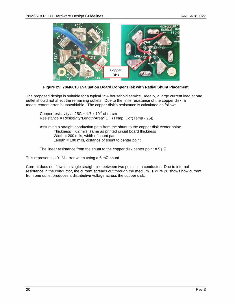
Figure 25: 78M6618 Evaluation Board Copper Disk with Radial Shunt Placement The proposed design is suitable for a typical 15A household service. Ideally, a large current load at one outlet should not affect the remaining outlets. Due to the finite resistance of the copper disk, a measurement error is unavoidable. The copper disk’s resistance is calculated as follows:
Copper resistivity at 25C = 1.7 x 10⁻⁶ ohm-cm Resistance = Resistivity*Length/Area*(1 + (Temp_Co*(Temp - 25))
Assuming a straight conduction path from the shunt to the copper disk center point:
Thickness = 62 mils, same as printed circuit board thickness Width = 200 mils, width of shunt pad Length = 100 mils, distance of shunt to center point
The linear resistance from the shunt to the copper disk center point = 5 µΩ This represents a 0.1% error when using a 6 mΩ shunt. Current does not flow in a single straight line between two points in a conductor. Due to internal resistance in the conductor, the current spreads out through the medium. Figure 26 shows how current from one outlet produces a distributive voltage across the copper disk.
Copper Disk

AN_6618_027 78M6618 PDU1 Hardware Design Guidelines
Rev. 3 21
Figure 26: Single Load Voltage Distribution in a Disk Observe how the presence of a current at one location (assume position 0 degrees), creates a small voltage at positions 45, 90, 135, 180, 225, 270 and 315 degrees (the other shunt locations). The shunts most affected by a single large load (at position 0 degrees) are the two adjacent shunts on the opposite side of the board (at positions 45 and 315 degrees). The above voltage distribution assumes no current flow in the other seven outlets. When current flows in two or more outlets, the current distribution through the copper disk depends on the difference between the adjacent currents. A small outlet current flowing next to a large outlet current will endure a non-linear measurement error due to the larger load’s current distribution implied in Figure 26. The smaller current’s path to the center point is no longer a straight line but a longer curved path. The longer curved path effectively reflects itself as additional resistance in the path from the shunt to the center point. The above condition exhibits itself when the relative current magnitudes approach 100:1. For example, a 10 A load at one outlet affects the accuracy of an adjacent 100 ma load. The 100 mA load will be measured as 105 mA. Similarly, a 1 A small load with a 10 A large load will be measured as 1.002 mA.
Series1
Series9 Series17
Series25
0
0.1
0.2
0.3
0.4
0.5
0.6
0.7
0.8
0.9
1
1 4 7 10 13 16 19 22 25 28 31
0.9-1
0.8-0.9
0.7-0.8
0.6-0.7
0.5-0.6
0.4-0.5
0.3-0.4
0.2-0.3
0.1-0.2
0-0.1
Outlet Current Exit Point
Edge of Disk
Source Current Inlet Point
Disk Center Point
78M6618 PDU1 Hardware Design Guidelines AN_6618_027
22 Rev 3
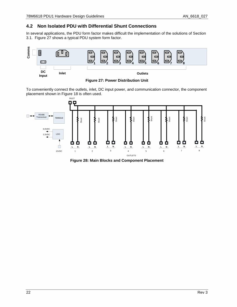
4.2 Non Isolated PDU with Differential Shunt Connections In several applications, the PDU form factor makes difficult the implementation of the solutions of Section 3.1. Figure 27 shows a typical PDU system form factor.
1 2 3 4 5 6 7 8
Inlet
Com
ms
OutletsDC Input
Figure 27: Power Distribution Unit To conveniently connect the outlets, inlet, DC input power, and communication connector, the component placement shown in Figure 18 is often used.
78M6618
LDO
12VDC
L N
7
L N
6
L N
5
L N
4
L N
3
L N
2
L N
1
L N
8
RS486Transceiver
6.6VDC
3.3VDC
Shu
nt
Shu
nt
Shu
nt
Shu
nt
Shu
nt
Shu
nt
Shu
nt
Shu
nt
OUTLETS
INLET
Figure 28: Main Blocks and Component Placement
AN_6618_027 78M6618 PDU1 Hardware Design Guidelines
Rev. 3 23
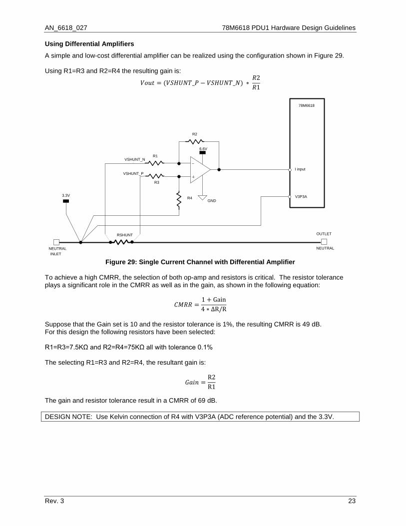
Using Differential Amplifiers
A simple and low-cost differential amplifier can be realized using the configuration shown in Figure 29. Using R1=R3 and R2=R4 the resulting gain is:
𝑉𝑜𝑢𝑡 = (𝑉𝑆𝐻𝑈𝑁𝑇_𝑃 − 𝑉𝑆𝐻𝑈𝑁𝑇_𝑁) ∗ 𝑅2𝑅1
RSHUNT
NEUTRAL
3.3V
R3
R1
R4
R2
6.6V
GND
I input
V3P3A
NEUTRAL
OUTLET
INLET
78M6618
VSHUNT_N
VSHUNT_P
Figure 29: Single Current Channel with Differential Amplifier
To achieve a high CMRR, the selection of both op-amp and resistors is critical. The resistor tolerance plays a significant role in the CMRR as well as in the gain, as shown in the following equation:
𝐶𝑀𝑅𝑅 =1 + Gain4 ∗ ∆R/R
Suppose that the Gain set is 10 and the resistor tolerance is 1%, the resulting CMRR is 49 dB. For this design the following resistors have been selected: R1=R3=7.5KΩ and R2=R4=75KΩ all with tolerance 0.1% The selecting R1=R3 and R2=R4, the resultant gain is:
𝐺𝑎𝑖𝑛 =R2R1
The gain and resistor tolerance result in a CMRR of 69 dB. DESIGN NOTE: Use Kelvin connection of R4 with V3P3A (ADC reference potential) and the 3.3V.
78M6618 PDU1 Hardware Design Guidelines AN_6618_027
24 Rev 3
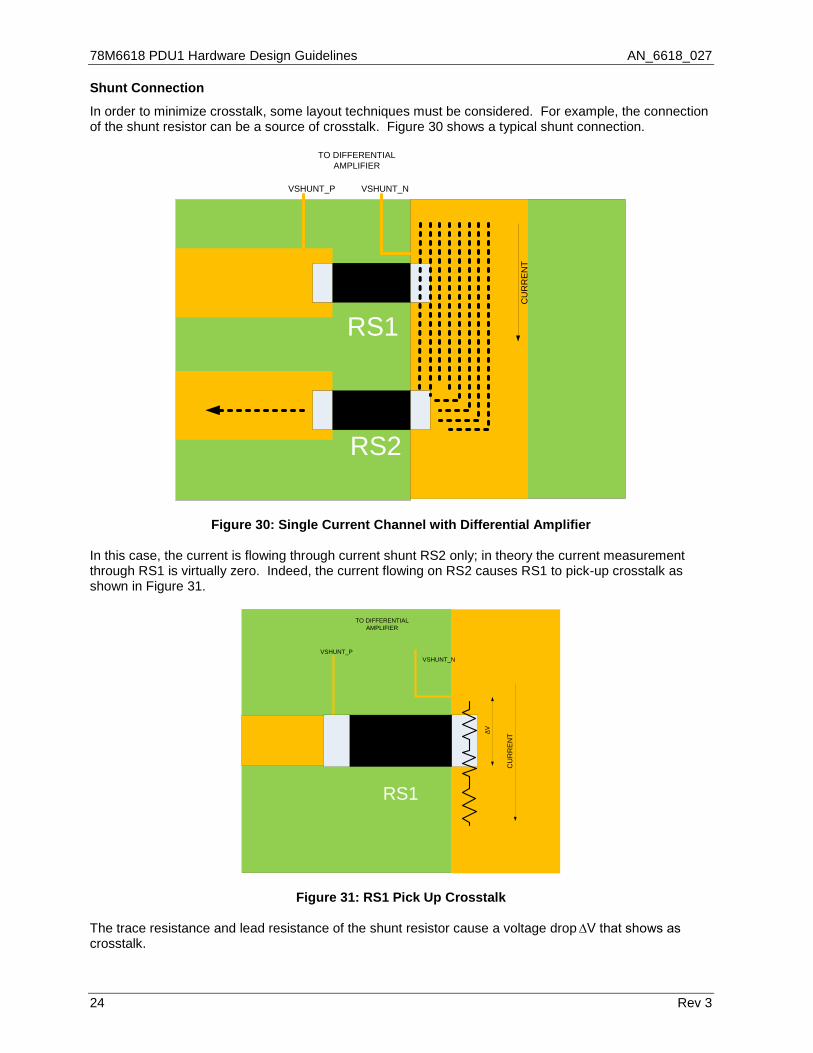
Shunt Connection
In order to minimize crosstalk, some layout techniques must be considered. For example, the connection of the shunt resistor can be a source of crosstalk. Figure 30 shows a typical shunt connection.
CU
RR
EN
T
TO DIFFERENTIAL AMPLIFIER
VSHUNT_P VSHUNT_N
RS1
RS2
Figure 30: Single Current Channel with Differential Amplifier In this case, the current is flowing through current shunt RS2 only; in theory the current measurement through RS1 is virtually zero. Indeed, the current flowing on RS2 causes RS1 to pick-up crosstalk as shown in Figure 31.
`RS1
TO DIFFERENTIAL AMPLIFIER
VSHUNT_PVSHUNT_N
RS1
CU
RR
EN
T∆V
Figure 31: RS1 Pick Up Crosstalk The trace resistance and lead resistance of the shunt resistor cause a voltage drop ∆V that shows as crosstalk.
AN_6618_027 78M6618 PDU1 Hardware Design Guidelines
Rev. 3 25
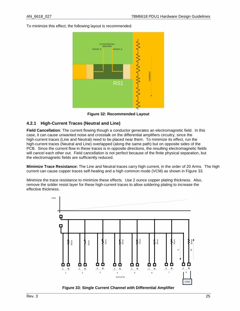
To minimize this effect, the following layout is recommended.
`RS1
TO DIFFERENTIAL AMPLIFIER
VSHUNT_P VSHUNT_N
RS1
CU
RR
EN
T
Figure 32: Recommended Layout
4.2.1 High-Current Traces (Neutral and Line) Field Cancellation: The current flowing though a conductor generates an electromagnetic field. In this case, it can cause unwanted noise and crosstalk on the differential amplifiers circuitry, since the high-current traces (Line and Neutral) need to be placed near them. To minimize its effect, run the high-current traces (Neutral and Line) overlapped (along the same path) but on opposite sides of the PCB. Since the current flow in these traces is in opposite directions, the resulting electromagnetic fields will cancel each other out. Field cancellation is not perfect because of the finite physical separation, but the electromagnetic fields are sufficiently reduced. Minimize Trace Resistance: The Line and Neutral traces carry high current, in the order of 20 Arms. The high current can cause copper traces self-heating and a high common mode (VCM) as shown in Figure 33. Minimize the trace resistance to minimize these effects. Use 2 ounce copper plating thickness. Also, remove the solder resist layer for these high-current traces to allow soldering plating to increase the effective thickness.
L N
7
L N
6
L N
5
L N
4
L N
3
L N
2
L N
1
L N
8
Shu
nt
Shu
nt
Shu
nt
Shu
nt
Shu
nt
Shu
nt
Shu
nt
Shu
nt
OUTLETS
LOAD
IL IN
VCM
Figure 33: Single Current Channel with Differential Amplifier
78M6618 PDU1 Hardware Design Guidelines AN_6618_027
26 Rev 3
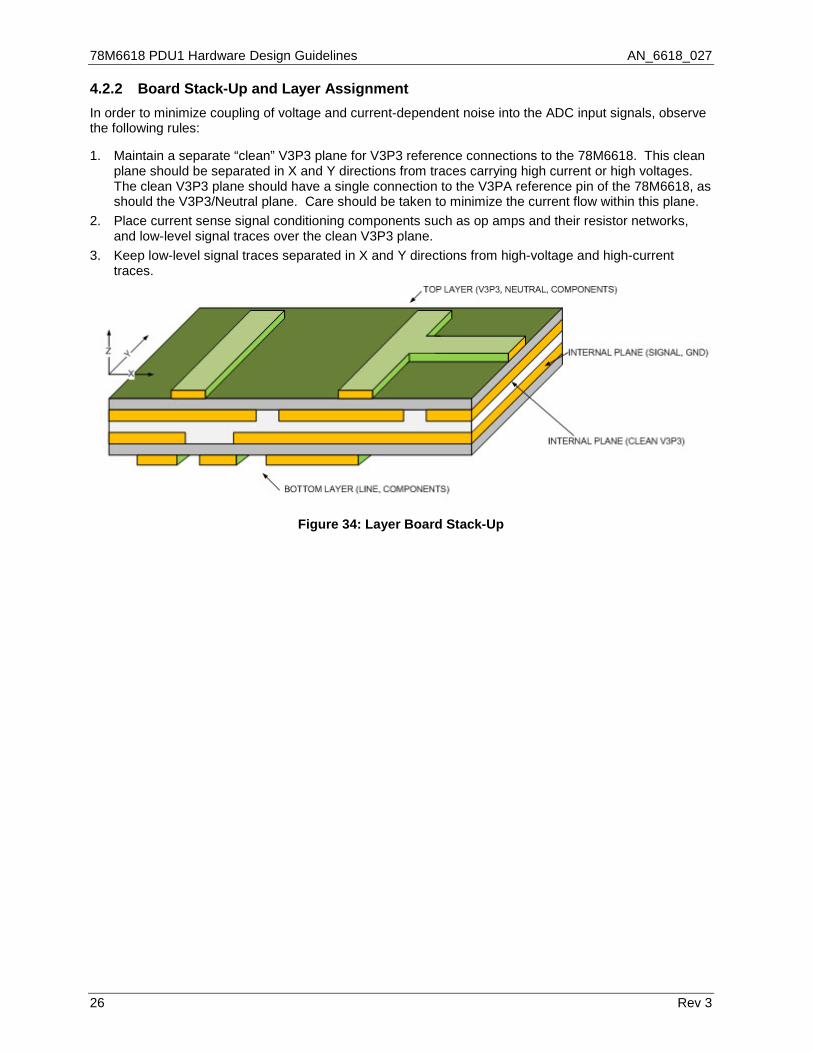
4.2.2 Board Stack-Up and Layer Assignment In order to minimize coupling of voltage and current-dependent noise into the ADC input signals, observe the following rules: 1. Maintain a separate “clean” V3P3 plane for V3P3 reference connections to the 78M6618. This clean
plane should be separated in X and Y directions from traces carrying high current or high voltages. The clean V3P3 plane should have a single connection to the V3PA reference pin of the 78M6618, as should the V3P3/Neutral plane. Care should be taken to minimize the current flow within this plane.
2. Place current sense signal conditioning components such as op amps and their resistor networks, and low-level signal traces over the clean V3P3 plane.
3. Keep low-level signal traces separated in X and Y directions from high-voltage and high-current traces.
Figure 34: Layer Board Stack-Up
AN_6618_027 78M6618 PDU1 Hardware Design Guidelines
Rev. 3 27
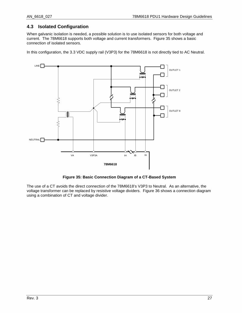
4.3 Isolated Configuration When galvanic isolation is needed, a possible solution is to use isolated sensors for both voltage and current. The 78M6618 supports both voltage and current transformers. Figure 35 shows a basic connection of isolated sensors. In this configuration, the 3.3 VDC supply rail (V3P3) for the 78M6618 is not directly tied to AC Neutral.
LINE
VA IBIHV3P3A
78M6618
IA
OUTLET 1
OUTLET 2
OUTLET 8
NEUTRAL
Figure 35: Basic Connection Diagram of a CT-Based System The use of a CT avoids the direct connection of the 78M6618’s V3P3 to Neutral. As an alternative, the voltage transformer can be replaced by resistive voltage dividers. Figure 36 shows a connection diagram using a combination of CT and voltage divider.
78M6618 PDU1 Hardware Design Guidelines AN_6618_027
28 Rev 3
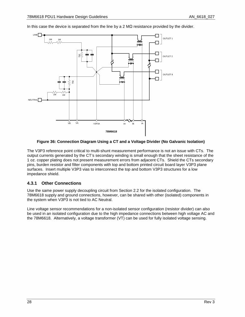
In this case the device is separated from the line by a 2 MΩ resistance provided by the divider.
Figure 36: Connection Diagram Using a CT and a Voltage Divider (No Galvanic Isolation) The V3P3 reference point critical to multi-shunt measurement performance is not an issue with CTs. The output currents generated by the CT’s secondary winding is small enough that the sheet resistance of the 1 oz. copper plating does not present measurement errors from adjacent CTs. Shield the CTs secondary pins, burden resistor and filter components with top and bottom printed circuit board layer V3P3 plane surfaces. Insert multiple V3P3 vias to interconnect the top and bottom V3P3 structures for a low impedance shield. 4.3.1 Other Connections Use the same power supply decoupling circuit from Section 2.2 for the isolated configuration. The 78M6618 supply and ground connections, however, can be shared with other (isolated) components in the system when V3P3 is not tied to AC Neutral. Line voltage sensor recommendations for a non-isolated sensor configuration (resistor divider) can also be used in an isolated configuration due to the high impedance connections between high voltage AC and the 78M6618. Alternatively, a voltage transformer (VT) can be used for fully isolated voltage sensing.
LINE
VA IBIHV3P3A
78M6618
IA
OUTLET 1
OUTLET 2
OUTLET 8
NEUTRAL
1M1M
1M 1M
750
VB
750

AN_6618_027 78M6618 PDU1 Hardware Design Guidelines
Rev. 3 29
5 Calibration Considerations All power measurement ICs must employ in-system calibration to achieve higher accuracy. In-system calibration compensates for the PCB trace lengths, LINE input voltage divider resistor network, current sensor tolerances and 78M6618 IC tolerances. Using tighter tolerance components can help reduce or even eliminate in-system calibration depending on the required measurement accuracy. As an example, the following table shows different levels of accuracies that can be achieved with different levels of calibration. The Current Only Calibration compensates for only the current sensing resistor tolerance and utilizes 0.1% tolerance resistors for the voltage sensor. The Full Calibration compensates for both the voltage divider plus the current sensor tolerances. If the system does not require a high level of accuracy relative to the initial tolerance of the voltage divider and current sensor components, predetermined coefficients can also be hard coded into the firmware to eliminate production line calibration and maximize cost savings.
Calibration Type Time Accuracy Full Calibration per outlet < 15s < 0.5% Current Only Calibration per outlet 1 < 7.5s < 1% No Calibration (fixed coeff.) 1 2 0 < 2.5
Notes:
1. Use 0.1% tolerance resistors voltage divider. 2. Use 1% tolerance shunt resistor or burden resistor when using a current transformer. 3. VT unit-to-unit variation typically requires Full Calibration. Refer to the 78M661x Calibration Procedure for additional information.
78M6618 PDU1 Hardware Design Guidelines AN_6618_027 Revision History Revision Date Description 1.0 4/16/2010 First publication. 1.1 8/31/2010 Added the Timing Reference section. 1.2 10/29/2010 Added the Voltage Transformers section. 2 11/4/2011 Added information about designing a power distribution unit to Section 2.2
and Section 2.5. Added Section 3.2.2, Board Stack-Up and Layer Assignment.
3 4/11/12 Deleted “Place the 1000 pF capacitor closest to the V3P3A pin of the 78M6618.” from page 3. Added “±” in front of “250” on page 7. Corrected the figure references for Figure 29, Figure 30, and Figure 31.
30Maxim Integrated 160 Rio Robles, San Jose, CA 95134 USA 1-408-601-1000
Maxim cannot assume responsibility for use of any circuitry other than circuitry entirely embodied in a Maxim product. No circuit patent licenses are implied. Maxim reserves the right to change the circuitry and specifications without notice at any time. The parametric values (min and max limits) shown in the Electrical Characteristics table are guaranteed. Other parametric values quoted in this data sheet are provided for guidance.
© 2012 Maxim Integrated The Maxim logo and Maxim Integrated are trademarks of Maxim Integrated Products, Inc.