HTS221 digital humidity sensor: hardware guidelines … · November 2015 DocID028002 Rev 1 1/14...
14
November 2015 DocID028002 Rev 1 1/14 www.st.com AN4722 Application note HTS221 digital humidity sensor: hardware guidelines for system integration Introduction This document introduces hardware guidelines and reference designs for integration of the HTS221 in final customer applications.
Transcript of HTS221 digital humidity sensor: hardware guidelines … · November 2015 DocID028002 Rev 1 1/14...
November 2015 DocID028002 Rev 1 1/14
www.st.com
AN4722 Application note
HTS221 digital humidity sensor: hardware guidelines for system integration
Introduction This document introduces hardware guidelines and reference designs for integration of the HTS221 in final customer applications.

Contents AN4722
2/14 DocID028002 Rev 1
Contents 1 System integration .......................................................................... 3
2 Mechanical design rules ................................................................. 4
2.1 Sensor placement ............................................................................. 4 2.1.1 Exposure to the environment ............................................................. 4 2.1.2 Heat propagation ................................................................................ 5 2.1.3 Mechanical stress ............................................................................... 8 2.1.4 Light exposure .................................................................................... 9
2.2 Sensor embodiment and housing ...................................................... 9
2.3 Sensor protection ............................................................................ 10
3 Reference design: thermal decoupling ........................................ 11
4 Revision history ............................................................................ 13
AN4722 System integration
DocID028002 Rev 1 3/14
1 System integration The integration of the HTS221 relative humidity sensor in portable devices (PDs) such as smart phones and wearable devices, or in weather stations or air conditioning equipment shall be implemented without compromising sensor performance. The main mechanical and geometric parameters in the final application must be considered as well as optimizing the factors that influence sensor performance.
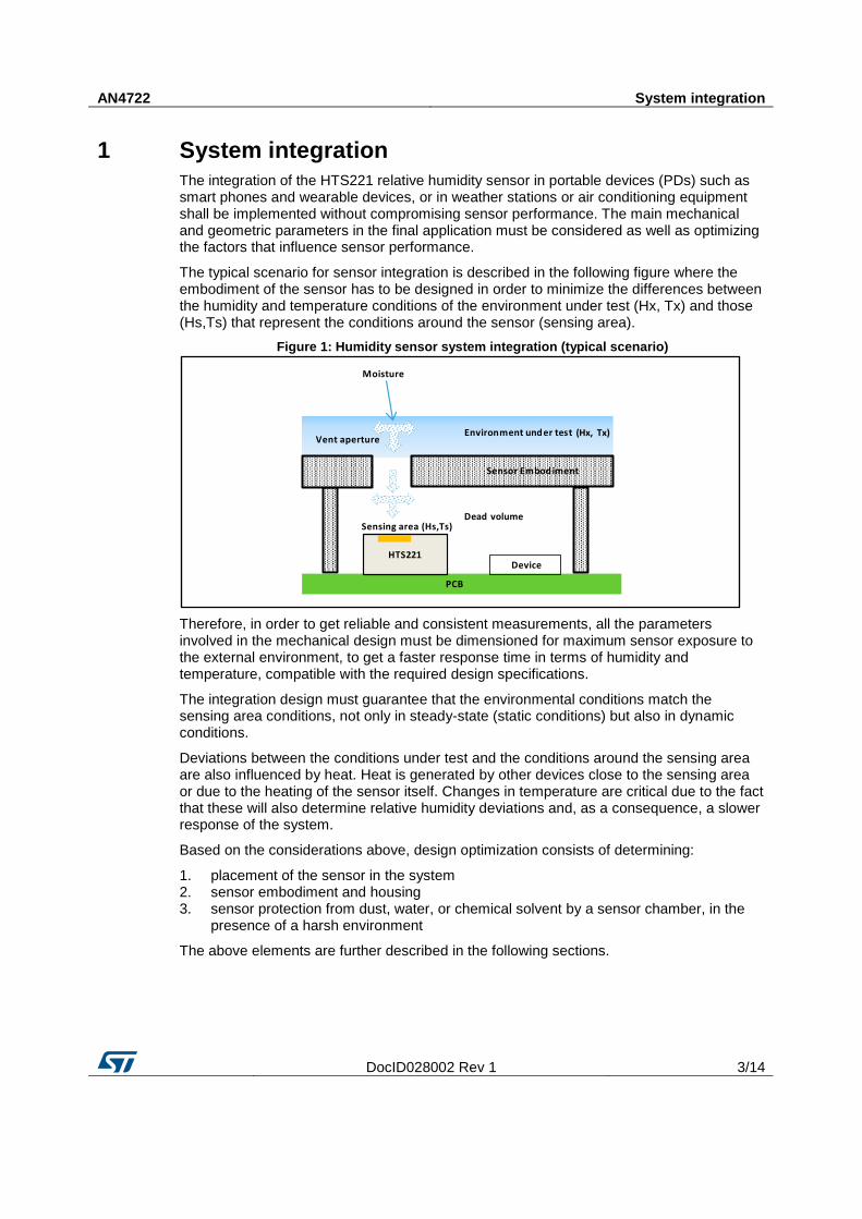
The typical scenario for sensor integration is described in the following figure where the embodiment of the sensor has to be designed in order to minimize the differences between the humidity and temperature conditions of the environment under test (Hx, Tx) and those (Hs,Ts) that represent the conditions around the sensor (sensing area).
Figure 1: Humidity sensor system integration (typical scenario)
Therefore, in order to get reliable and consistent measurements, all the parameters involved in the mechanical design must be dimensioned for maximum sensor exposure to the external environment, to get a faster response time in terms of humidity and temperature, compatible with the required design specifications.
The integration design must guarantee that the environmental conditions match the sensing area conditions, not only in steady-state (static conditions) but also in dynamic conditions.
Deviations between the conditions under test and the conditions around the sensing area are also influenced by heat. Heat is generated by other devices close to the sensing area or due to the heating of the sensor itself. Changes in temperature are critical due to the fact that these will also determine relative humidity deviations and, as a consequence, a slower response of the system.
Based on the considerations above, design optimization consists of determining:
1. placement of the sensor in the system 2. sensor embodiment and housing 3. sensor protection from dust, water, or chemical solvent by a sensor chamber, in the
presence of a harsh environment
The above elements are further described in the following sections.
HTS221
Environment under test
Sensing area (Hs,Ts)
PCB
Device
Vent aperture
Sensor Embodiment
Moisture
Dead volume
(Hx, Tx)

Mechanical design rules AN4722
4/14 DocID028002 Rev 1
2 Mechanical design rules In the mechanical design the main constraints and features to be considered are described below with the purpose of introducing a set of basic rules as good design practices for successfully integrating the sensor in a final application.
2.1 Sensor placement Placement of the sensor has a direct impact on its performance due to proximity and exposure to the environment, heat generation, and mechanical stress.
2.1.1 Exposure to the environment Placement of the sensor must be to maximize its exposure to the environment where humidity and temperature are measured, in static and dynamic operating conditions.
In static conditions (steady-state) after a change in the humidity and temperature environment and their stabilization, sensing conditions must be at the same as those of the conditions under test, or very close to the target value, depending on the application tolerance and specifications.
In dynamic conditions, (in presence of fast changes of the conditions under test), the sensor must be able to provide a reliable measurement output able to follow the dynamic of the environment. At the end of the sensor integration design, the overall response time will be modified, and the final performance shall match the target specifications. In general, the target is to design with a response time shorter than the product specifications.
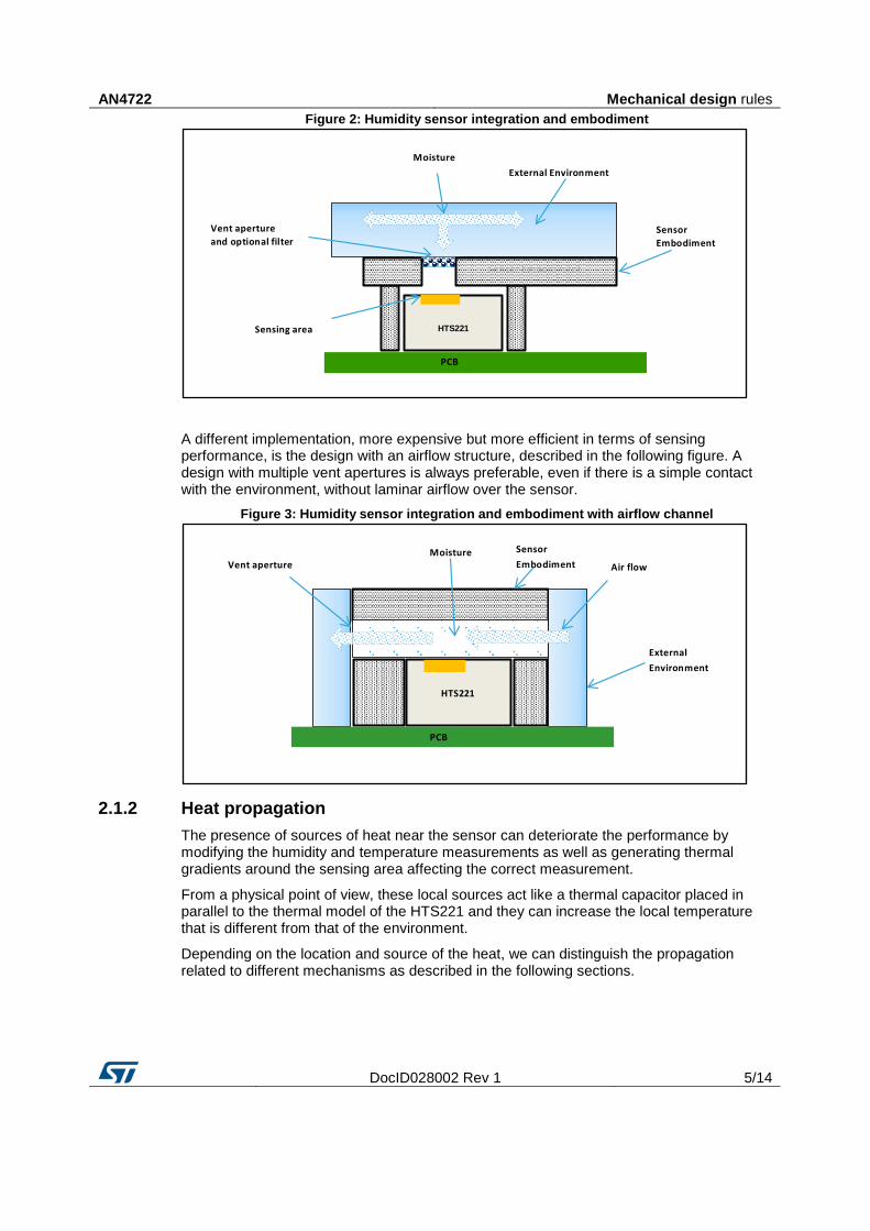
In order to maximize sensor performance in static and dynamic conditions after system integration, depending on the design specifications, the below guidelines are recommended (refer to Figure 2: "Humidity sensor integration and embodiment").
1. Place the sensor to get the best connection with exposure to the environment under test (as close as possible to the vent aperture)
2. Large dead volume will increase the humidity response time significantly, therefore it is recommended to minimize the volume, trying to shape a tailored housing around the perimeter of the sensor
3. Vent aperture should be as large as possible; an order of magnitude lower than the sensing element geometry represents a reasonable integration form factor.
4. Depth of the vent aperture must be minimized. The aperture dimensions significantly affect humidity response time.
5. Materials that can absorb humidity have to be avoided in the dead volume
As a reference design, Figure 2: "Humidity sensor integration and embodiment" illustrates an example of the above recommendations. In order to maximize exposure to the environment and therefore obtain a faster response time, the volume around the sensor (dead volume) is minimized and the vent size aperture has the same order of magnitude as that of the sensing area. A filter membrane protection has been added, for protecting the sensor from water or a harsh environment.
AN4722 Mechanical design rules
DocID028002 Rev 1 5/14
Figure 2: Humidity sensor integration and embodiment
A different implementation, more expensive but more efficient in terms of sensing performance, is the design with an airflow structure, described in the following figure. A design with multiple vent apertures is always preferable, even if there is a simple contact with the environment, without laminar airflow over the sensor.
Figure 3: Humidity sensor integration and embodiment with airflow channel
2.1.2 Heat propagation The presence of sources of heat near the sensor can deteriorate the performance by modifying the humidity and temperature measurements as well as generating thermal gradients around the sensing area affecting the correct measurement.
From a physical point of view, these local sources act like a thermal capacitor placed in parallel to the thermal model of the HTS221 and they can increase the local temperature that is different from that of the environment.
Depending on the location and source of the heat, we can distinguish the propagation related to different mechanisms as described in the following sections.
MoistureExternal Environment
Vent apertureand optional filter
Sensor Embodiment
Sensing area HTS221
SensorEmbodiment
PCB
ExternalEnvironment
MoistureVent aperture
HTS221
SensorEmbodiment
PCB
Air flow

Mechanical design rules AN4722
6/14 DocID028002 Rev 1
Convective heat Local thermal sources around the sensor can modify humidity and temperature measurements by radiating heat which increases the temperature of the sensing area.
Typical sources are as follows:
• other sensors and devices placed close to the humidity sensor • power management devices • processors and microcontrollers • LCD displays that, in particular, provide a significant temperature gradient between the
environment and the dead volume inside the system
Therefore the sensor has to be placed at the correct distance from these heat sources, and in order to guarantee appropriate insulation, it is recommended to adopt inside the embodiment thermal insulation structures as described in the following figure. It is also recommended, according to the specific layout, to implement a vent aperture close to the heat source, acting as a cooling channel.
Figure 4: Insulation implemented for protecting the sensor
Looking at a section of the sensor housing, the following figure shows a good design with the thermal insulation structure on the left, the heat source is far from the sensor and a thermal protection structure is placed in the middle. On the right an incorrect design is illustrated, which would allow heat generated by the component to reach the sensing area. Figure 5: Top view of the sensor housing (on the left, a correct design with insulation, on the
right, an incorrect design)
Cooling channel
HTS221
Environment under test
Sensing area
PCB
Devices
Vent aperture
Insul ation
AN4722 Mechanical design rules
DocID028002 Rev 1 7/14
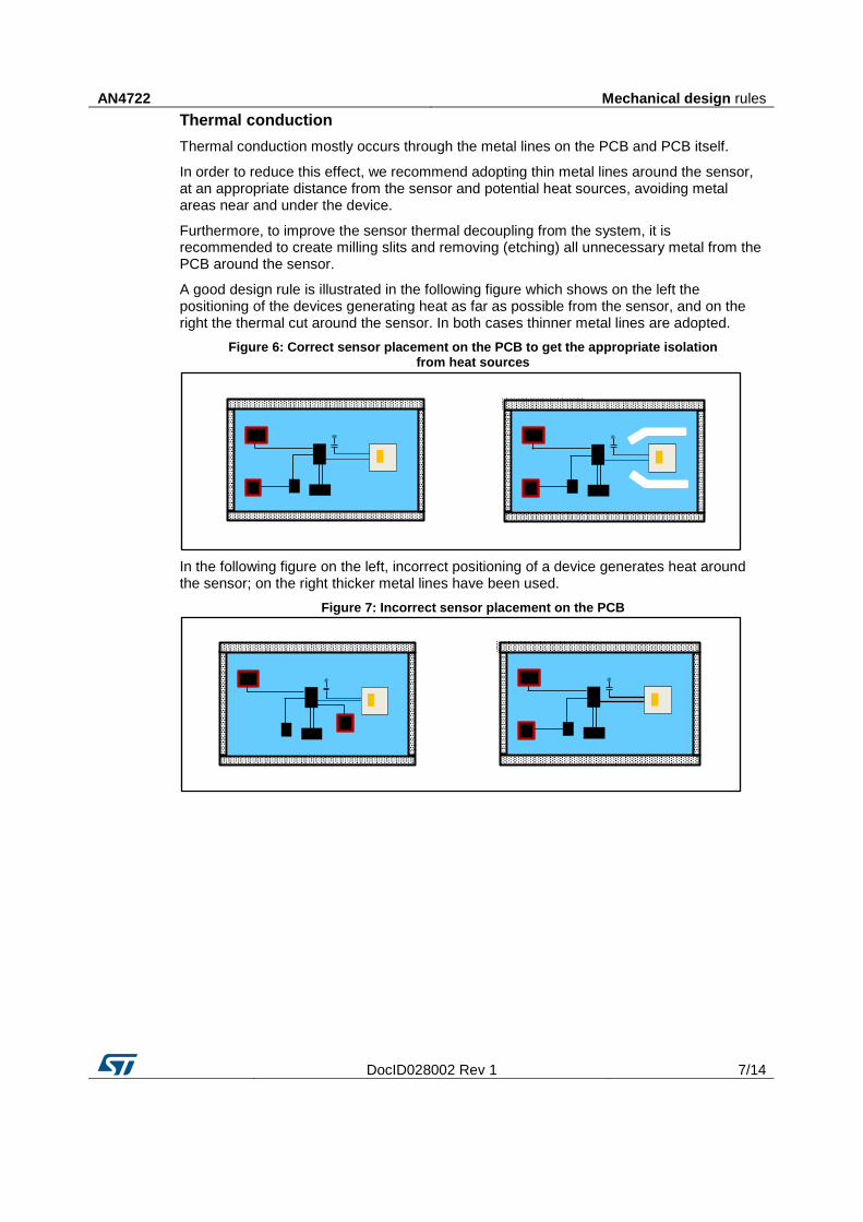
Thermal conduction Thermal conduction mostly occurs through the metal lines on the PCB and PCB itself.
In order to reduce this effect, we recommend adopting thin metal lines around the sensor, at an appropriate distance from the sensor and potential heat sources, avoiding metal areas near and under the device.
Furthermore, to improve the sensor thermal decoupling from the system, it is recommended to create milling slits and removing (etching) all unnecessary metal from the PCB around the sensor.
A good design rule is illustrated in the following figure which shows on the left the positioning of the devices generating heat as far as possible from the sensor, and on the right the thermal cut around the sensor. In both cases thinner metal lines are adopted.
Figure 6: Correct sensor placement on the PCB to get the appropriate isolation from heat sources
In the following figure on the left, incorrect positioning of a device generates heat around the sensor; on the right thicker metal lines have been used.
Figure 7: Incorrect sensor placement on the PCB

Mechanical design rules AN4722
8/14 DocID028002 Rev 1
Figure 8: Thermal cut of PCB (HTS221 DIL24 board) for reducing heat propagation through PCB
In both cases of thermal propagation, an infrared thermal analysis of the whole system, running under different operating conditions, is the recommended approach for identifying the appropriate location of the sensor.
2.1.3 Mechanical stress Placement of the sensor shall be such to avoid any mechanical force applied to the sensor, either directly due to an incorrect design of the mechanical system, or indirectly due to user interaction with the system as in the case of wearables or portable devices.
Figure 9: Incorrect configuration for mechanical stress
Figure 10: Correct configuration for avoiding mechanical stress
and reducing the dead volume
The figures above show correct and incorrect integration cases where, with the goal to reduce the dead volume around the sensor to improve the humidity response time, the embodiment structure is directly in contact with the sensor package, creating a mechanical stress that can affect sensor performance. A minimal clearance has to be maintained as in Figure 10: "Correct configuration for avoiding mechanical stress and reducing the dead volume" to avoid any force applied on the sensor and minimize the dead volume as well.
Thermal cutof the PCB
HTS221 HTS221
HTS221
PCB
HTS221
PCB

AN4722 Mechanical design rules
DocID028002 Rev 1 9/14
2.1.4 Light exposure Direct exposure of the sensor to light should be avoided, in order not to modify the temperature and as a consequence the humidity conditions.
2.2 Sensor embodiment and housing The sensor embodiment in the system shall match as much as possible the recommendations previously highlighted for sensor placement and, on top of that, shall meet the requirements of specific applications such as being waterproof, water-resistant or resistant to a harsh environment.
Furthermore, the design for the end user shall guarantee the air circulation from the environment to the sensing area, first from the environment (outside) to the end-user's device (inside), then internally from the aperture to the sensor housing and sensing element as well. The more efficient the air circulation in this path, the better the performance will be.
The air path shall be well identified and sized in order to maximize the airflow, and as a result the final performance of the integrated system.
The following figures summarize best design practices of sensor embodiment and housing. The figure below also includes an optional filter membrane and PCB cut to increase thermal decoupling.
Figure 11: Correct sensor embodiment and housing
Figure 12: Correct sensor embodiment and housing with airflow channel
Dead Volumeminimized to improvethe response time
Thermal barrierfor Heatprotection
Vent aperture(s) should be aslarge as possible, depending onthe specif requirements.Ventaperture depth has to beminimized.
HTS221
PCB
Device Device
External Environment
Moisture
Milling Slits for increasingThermal d ecoupling
Hydophobic/Du st orWaterp roof o ptionalmemb rane fil ter
Airflow
Milling Slits for increasingThermal d ecoupling
ExternalEnvironment
MoistureVent apertures
HTS221
SensorEmbodiment
PCB

Mechanical design rules AN4722
10/14 DocID028002 Rev 1
In addition Figure 12: "Correct sensor embodiment and housing with airflow channel" illustrates a more efficient implementation with two vent apertures which provide an airflow channel over the sensing area that results in higher efficiency in terms of response time.
In Figure 13: "Incorrect sensor embodiment and housing" a completely wrong design is illustrated, with very low efficiency in the final design, and sensor performance affected by heat coming from other devices.
Figure 13: Incorrect sensor embodiment and housing
2.3 Sensor protection An optional filter, which serves as a sensor chamber, can be adopted as sensor protection from dust, water, or chemical solvent, in presence of a harsh environment or for a waterproof application. The key parameter for this kind of implementation is the appropriate choice of the membrane, according to the design requirements and taking into account that the membrane material will provide a slower response time, particularly in terms of humidity response time.
Vent aperture(s) too far fromthe sensor and with a wronggeometry determining a tooslow response time
HTS221
Sensing area
PCB
Device
External Environment
Heating from otherdevices will affectoverall performance
Dead Volume too largedetermining a too slowresponse time

AN4722 Reference design: thermal decoupling
DocID028002 Rev 1 11/14
3 Reference design: thermal decoupling As previously recommended, we strongly advise monitoring the sources of heat under different operating conditions by infrared camera, and /or thermistors placed in key positions. The following figures show the infrared image and the corresponding layout of an electronic board where the HTS221 has been mounted.
Placement is implemented by following the basic rules previously described, mounting the sensor as far as possible from the main sources of heat present on the board. As highlighted in the infrared picture, the LDO and the microcontroller represent the most significant sources of heat and they are far from the HTS221 that was positioned in the left bottom corner.
Figure 14: HTS221 placement and thermal (infrared) view
Another approach to improve the thermal decoupling of the sensor is by mounting it on a flex board as described in the figure below. This implementation will drastically reduce heat conduction and radiation of heat as well.
Figure 15: HTS221 on flex board
Based on the previous recommendations, the following figure shows correct placement of the HTS221 with respect to other devices on the PCB: the PDs are recommended to be placed in a corner where the choice of an implementation with an airflow channel is not expensive, allowing best sensor performance. Harsh environments require that the sensor be mounted inside a sensor chamber (SMC) with vent apertures (protected by membranes) as illustrated in the following figure.
Reference design: thermal decoupling AN4722
12/14 DocID028002 Rev 1
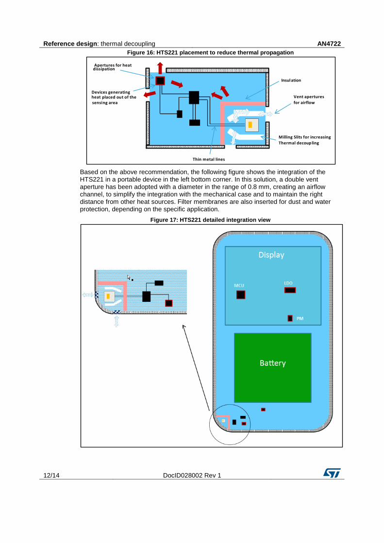
Figure 16: HTS221 placement to reduce thermal propagation
Based on the above recommendation, the following figure shows the integration of the HTS221 in a portable device in the left bottom corner. In this solution, a double vent aperture has been adopted with a diameter in the range of 0.8 mm, creating an airflow channel, to simplify the integration with the mechanical case and to maintain the right distance from other heat sources. Filter membranes are also inserted for dust and water protection, depending on the specific application.
Figure 17: HTS221 detailed integration view
Apertures for heatdissipation
Insul ation
Devices generatingheat placed out of thesensing area
Vent aperturesfor airflow
Milling Slits for increasingThermal decoupling
Thin metal lines

AN4722 Revision history
DocID028002 Rev 1 13/14
4 Revision history Table 1: Document revision history
Date Revision Changes
09-Nov-2015 1 Initial release.
AN4722
14/14 DocID028002 Rev 1
IMPORTANT NOTICE – PLEASE READ CAREFULLY
STMicroelectronics NV and its subsidiaries (“ST”) reserve the right to make changes, corrections, enhancements, modifications, and improvements to ST products and/or to this document at any time without notice. Purchasers should obtain the latest relevant information on ST products before placing orders. ST products are sold pursuant to ST’s terms and conditions of sale in place at the time of order acknowledgement.
Purchasers are solely responsible for the choice, selection, and use of ST products and ST assumes no liability for application assistance or the design of Purchasers’ products.
No license, express or implied, to any intellectual property right is granted by ST herein.
Resale of ST products with provisions different from the information set forth herein shall void any warranty granted by ST for such product.
ST and the ST logo are trademarks of ST. All other product or service names are the property of their respective owners.
Information in this document supersedes and replaces information previously supplied in any prior versions of this document.
© 2015 STMicroelectronics – All rights reserved