7-Series Architecture Overview -...
65
This material exempt per Department of Commerce license exception TSU Zynq Vivado 2013.2 Version 7-Series Architecture Overview © Copyright 2013 Xilinx
Transcript of 7-Series Architecture Overview -...

This material exempt per Department of Commerce license exception TSU
Zynq Vivado 2013.2 Version
7-Series Architecture Overview
© Copyright 2013 Xilinx
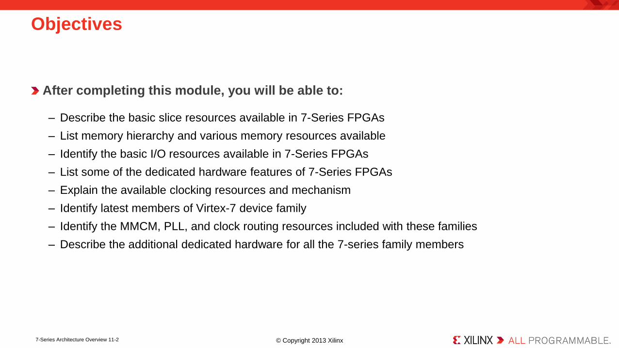
After completing this module, you will be able to:
– Describe the basic slice resources available in 7-Series FPGAs
– List memory hierarchy and various memory resources available
– Identify the basic I/O resources available in 7-Series FPGAs
– List some of the dedicated hardware features of 7-Series FPGAs
– Explain the available clocking resources and mechanism
– Identify latest members of Virtex-7 device family
– Identify the MMCM, PLL, and clock routing resources included with these families
– Describe the additional dedicated hardware for all the 7-series family members
Objectives
© Copyright 2013 Xilinx 7-Series Architecture Overview 11-2

Introduction to 7-Series FPGA
Logic Resources
I/O Resources
Memory and DSP48 Resources
XADC
Clocking Resources
Zynq Family
Summary
Outline
© Copyright 2013 Xilinx 7-Series Architecture Overview 11-3

All Xilinx FPGAs contain the same basic resources – Logic Resources
• Slices (grouped into configurable logic blocks (CLB)) Contain combinatorial logic and register resources
• Memory
• Multipliers
– Interconnect Resources • Programmable interconnect
• IOBs Interface between the FPGA and the outside world
– Other resources • Global clock buffers
• Boundary scan logic
Through various generations, Xilinx added new architectural resources to target various
markets and application areas
Introduction
© Copyright 2013 Xilinx 7-Series Architecture Overview 11-4

7-Series FPGA Families
© Copyright 2013 Xilinx 7-Series Architecture Overview 11-5
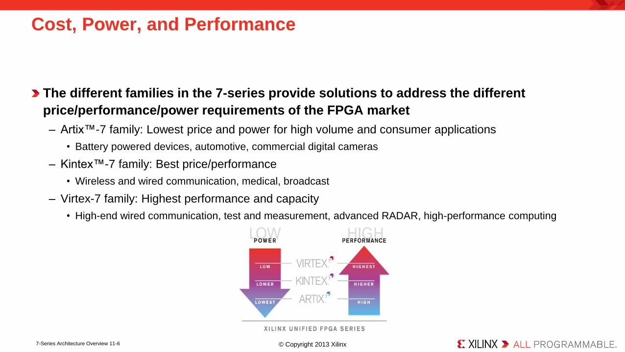
The different families in the 7-series provide solutions to address the different
price/performance/power requirements of the FPGA market
– Artix™-7 family: Lowest price and power for high volume and consumer applications
• Battery powered devices, automotive, commercial digital cameras
– Kintex™-7 family: Best price/performance
• Wireless and wired communication, medical, broadcast
– Virtex-7 family: Highest performance and capacity
• High-end wired communication, test and measurement, advanced RADAR, high-performance computing
Cost, Power, and Performance
© Copyright 2013 Xilinx 7-Series Architecture Overview 11-6
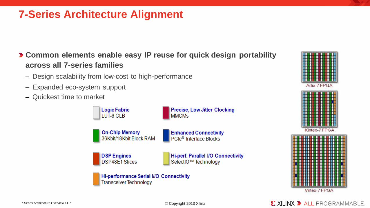
Common elements enable easy IP reuse for quick design portability
across all 7-series families
– Design scalability from low-cost to high-performance
– Expanded eco-system support
– Quickest time to market
7-Series Architecture Alignment
© Copyright 2013 Xilinx 7-Series Architecture Overview 11-7
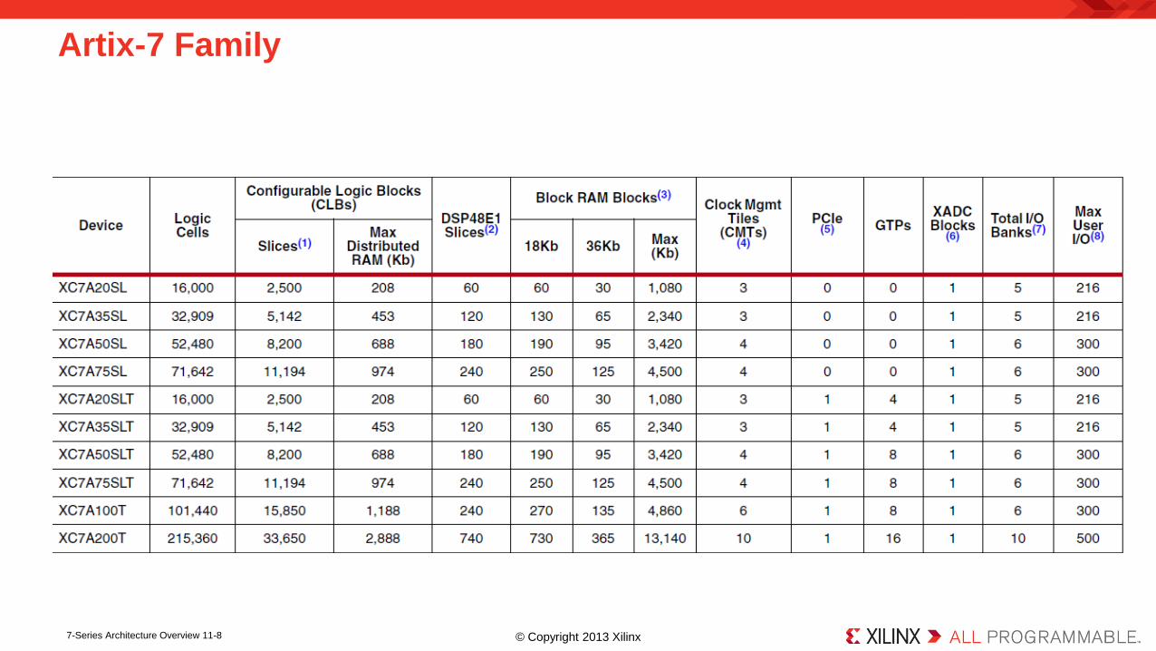
Artix-7 Family
© Copyright 2013 Xilinx 7-Series Architecture Overview 11-8

Artix-7 FPGA Architecture Overview
© Copyright 2013 Xilinx 7-Series Architecture Overview 11-9
Introduction to 7-Series FPGA
Logic Resources
I/O Resources
Memory and DSP48 Resources
XADC
Clocking Resources
Zynq Family
Summary
Outline
© Copyright 2013 Xilinx 7-Series Architecture Overview 11-10
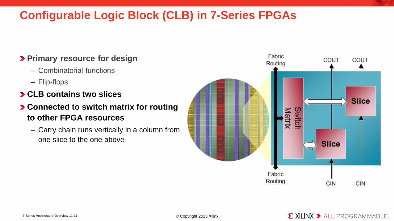
Primary resource for design
– Combinatorial functions
– Flip-flops
CLB contains two slices
Connected to switch matrix for routing
to other FPGA resources
– Carry chain runs vertically in a column from
one slice to the one above
Configurable Logic Block (CLB) in 7-Series FPGAs
© Copyright 2013 Xilinx 7-Series Architecture Overview 11-11

Two types of slices
– SLICEM: Full slice
LUT can be used for logic and memory/SRL
Has wide multiplexers and carry chain
– SLICEL: Logic and arithmetic only
LUT can only be used for logic (not memory)
Has wide multiplexers and carry chain
Two Types of Slices
© Copyright 2013 Xilinx 7-Series Architecture Overview 11-12

Four six-input Look-Up Tables (LUT)
Multiplexers
Carry chains
SRL
– Cascade path is not shown
Four flip-flops/latches
– Four additional flip-flops
The implementation tool will pack
multiple slices in the same CLB if
certain rules are followed
Slice Resource
© Copyright 2013 Xilinx 7-Series Architecture Overview 11-13
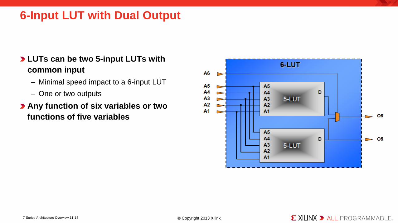
LUTs can be two 5-input LUTs with
common input
– Minimal speed impact to a 6-input LUT
– One or two outputs
Any function of six variables or two
functions of five variables
6-Input LUT with Dual Output
© Copyright 2013 Xilinx 7-Series Architecture Overview 11-14

Each F7MUX combines the outputs of two
LUTs together
– Can implement an arbitrary 7-input function
– Can implement an 8-1 multiplexer
The F8MUX combines the outputs of the
two F7MUXes
– Can implement an arbitrary 8-input function
– Can implement a 16-1 multiplexer
MUX is controlled by the BX/CX/DX slice
input
MUX output can drive out combinatorially
or to the flip-flop/latch
Wide Multiplexers
© Copyright 2013 Xilinx 7-Series Architecture Overview 11-15
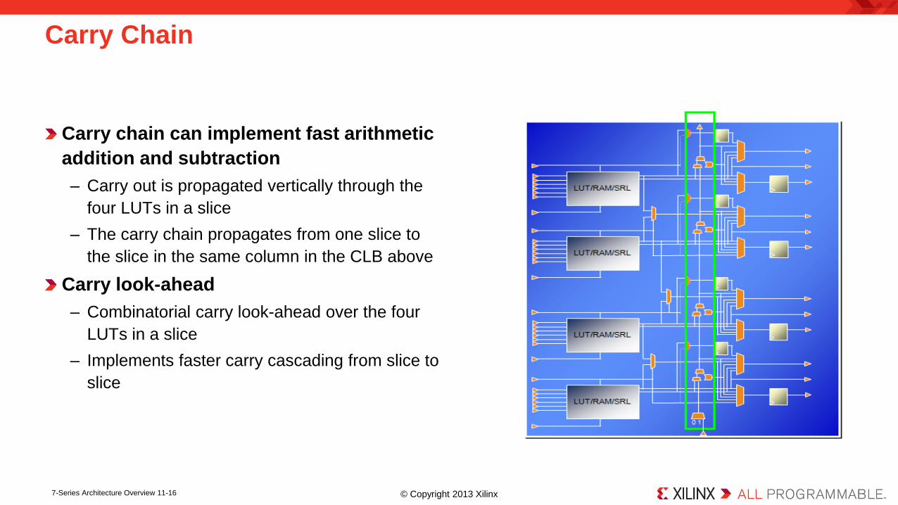
Carry chain can implement fast arithmetic
addition and subtraction
– Carry out is propagated vertically through the
four LUTs in a slice
– The carry chain propagates from one slice to
the slice in the same column in the CLB above
Carry look-ahead
– Combinatorial carry look-ahead over the four
LUTs in a slice
– Implements faster carry cascading from slice to
slice
Carry Chain
© Copyright 2013 Xilinx 7-Series Architecture Overview 11-16

Each slice has four flip-flop/latches (FF/L)
– Can be configured as either flip-flops or latches
– The D input can come from the O6 LUT output,
the carry chain, the wide multiplexer, or the
AX/BX/CX/DX slice input
Each slice also has four flip-flops (FF)
– D input can come from O5 output or the
AX/BX/CX/DX input
• These don’t have access to the carry chain, wide
multiplexers, or the slice inputs
If any of the FF/L are configured as
latches, the four FFs are not available
Slice Flip-Flops and Flip-Flop/Latches
© Copyright 2013 Xilinx 7-Series Architecture Overview 11-17
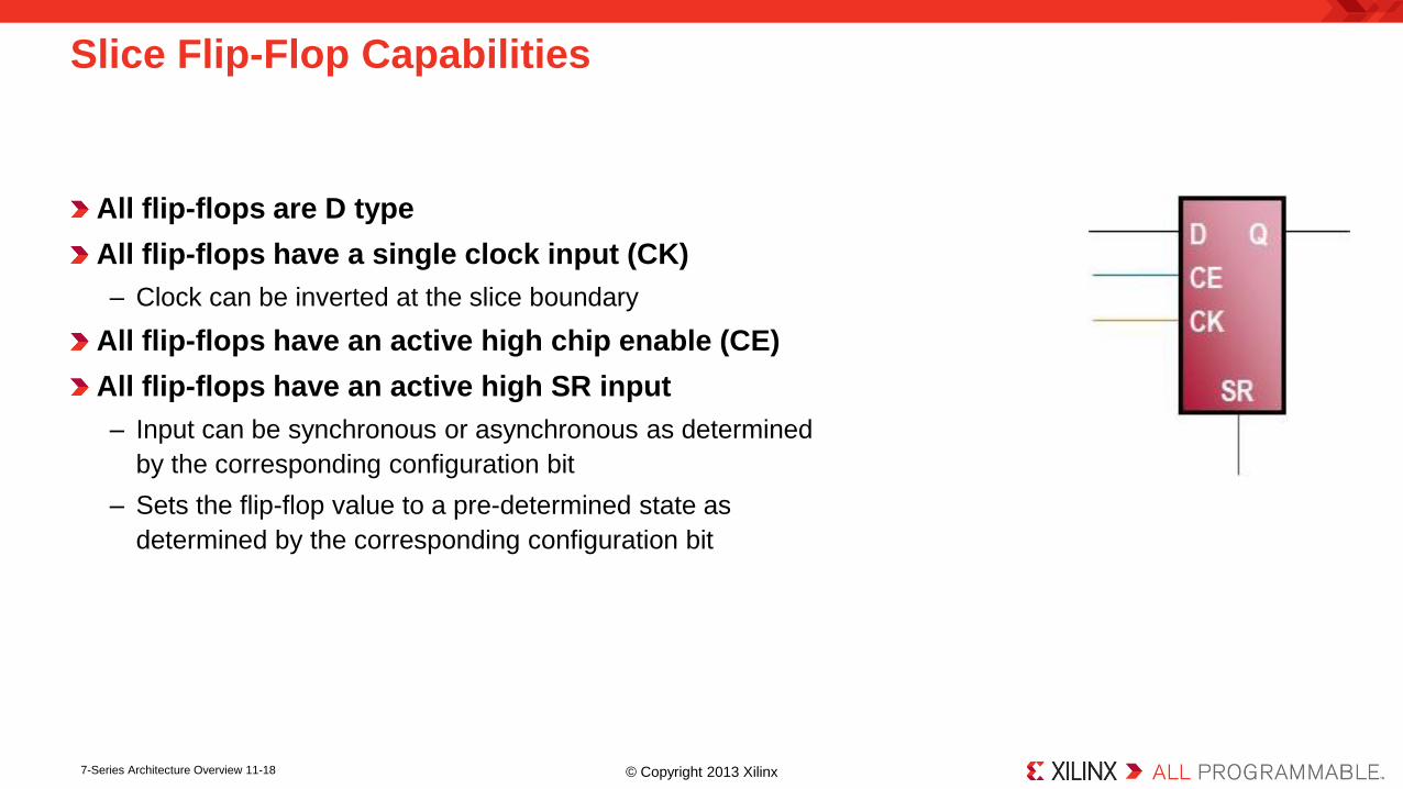
All flip-flops are D type
All flip-flops have a single clock input (CK)
– Clock can be inverted at the slice boundary
All flip-flops have an active high chip enable (CE)
All flip-flops have an active high SR input
– Input can be synchronous or asynchronous as determined
by the corresponding configuration bit
– Sets the flip-flop value to a pre-determined state as
determined by the corresponding configuration bit
Slice Flip-Flop Capabilities
© Copyright 2013 Xilinx 7-Series Architecture Overview 11-18

All flip-flops and flip-flop/latches share the same CK, SR, and CE
signals
– This is referred to as the "control set" of the flip-flops
– CE and SR are active high
– CK can be inverted at the slice boundary
If any one flip-flop uses a CE, all others must use the same CE
– CE gates the clock at the slice boundary
– Saves power
If any one flip-flop uses the SR, all others must use the same SR
– The reset value used for each flip-flop is individually set by the SRVAL
attribute
Control Sets
© Copyright 2013 Xilinx 7-Series Architecture Overview 11-19
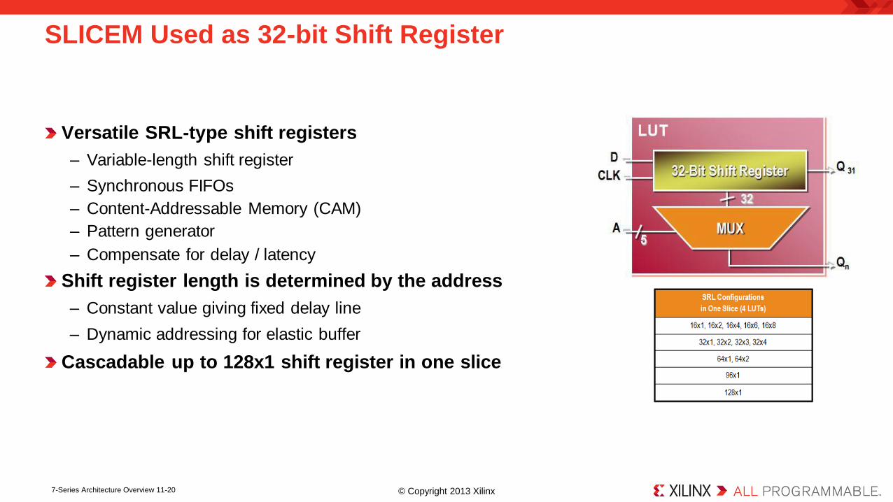
Versatile SRL-type shift registers
– Variable-length shift register
– Synchronous FIFOs
– Content-Addressable Memory (CAM)
– Pattern generator
– Compensate for delay / latency
Shift register length is determined by the address
– Constant value giving fixed delay line
– Dynamic addressing for elastic buffer
Cascadable up to 128x1 shift register in one slice
SLICEM Used as 32-bit Shift Register
© Copyright 2013 Xilinx 7-Series Architecture Overview 11-20
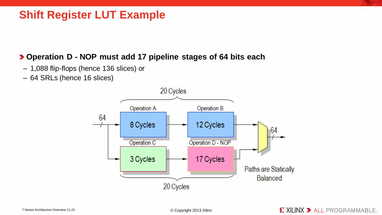
Operation D - NOP must add 17 pipeline stages of 64 bits each
– 1,088 flip-flops (hence 136 slices) or
– 64 SRLs (hence 16 slices)
Shift Register LUT Example
© Copyright 2013 Xilinx 7-Series Architecture Overview 11-21
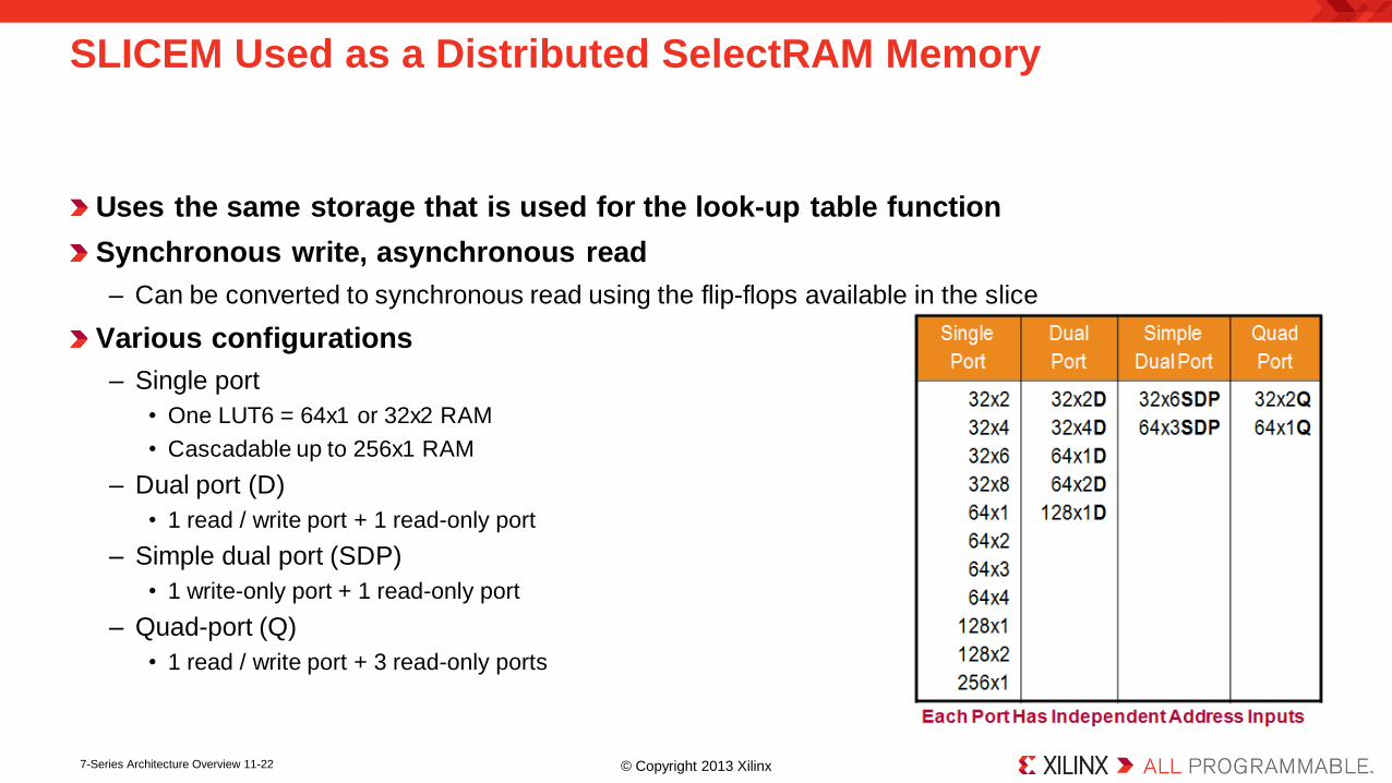
Uses the same storage that is used for the look-up table function
Synchronous write, asynchronous read
– Can be converted to synchronous read using the flip-flops available in the slice
Various configurations
– Single port
• One LUT6 = 64x1 or 32x2 RAM
• Cascadable up to 256x1 RAM
– Dual port (D)
• 1 read / write port + 1 read-only port
– Simple dual port (SDP)
• 1 write-only port + 1 read-only port
– Quad-port (Q)
• 1 read / write port + 3 read-only ports
SLICEM Used as a Distributed SelectRAM Memory
© Copyright 2013 Xilinx 7-Series Architecture Overview 11-22
Introduction to 7-Series FPGA
Logic Resources
I/O Resources
Memory and DSP48 Resources
XADC
Clocking Resources
Zynq FPGA
Summary
Outline
© Copyright 2013 Xilinx 7-Series Architecture Overview 11-23
High-speed operation with maintained signal integrity
– Source-synchronous operation (clock forwarding)
– System-synchronous operation (common systems clock)
– Terminate transmission lines to avoid signal reflections
Drive and receive data on wide parallel buses
– Compensate for bus skew and clock timing errors
– Conversion between serial and parallel data
– Achieve very high bit rate (> 1 Gbps)
Single Data Rate (SDR) or Double Data Rate (DDR) interfaces
Interface to many different standards
– Different voltages, drive strengths and protocols
I/O Interface Challenges
© Copyright 2013 Xilinx 7-Series Architecture Overview 11-24

7-Series FPGA I/O
Wide range of voltages
– 1.2V to 3.3V operation
Many different I/O standards
– Single ended and differential
– Referenced inputs
– 3-state support
Very high performance
– Up to 1600 Mbps LVDS
– Up to 1866 Mbps single-ended for DDR3
Easy interfacing to standard memories
– Hardware support for QDRII+ and DDR3
Digitally controlled impedance
Low power
– Features to reduce power
© Copyright 2013 Xilinx 7-Series Architecture Overview 11-25
I/O Block Diagram
© Copyright 2013 Xilinx 7-Series Architecture Overview 11-26

Two different types of I/O in 7-series FPGAs
– High Range (HR)
• Supports I/O standards with Vcco voltages up to 3.3V
– High Performance (HP)
• Supports I/O standards with Vcco voltages up to 1.8V only
• Designed for the highest performance
• Has ODELAY and DCI capability
I/O Types
© Copyright 2013 Xilinx 7-Series Architecture Overview 11-27
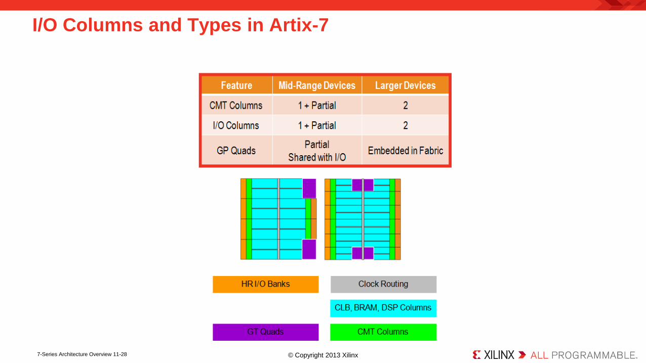
I/O Columns and Types in Artix-7
© Copyright 2013 Xilinx 7-Series Architecture Overview 11-28

P and N pins can be configured as
– Individual single-ended signals or
– Differential pair
Receiver can be standard CMOS or
voltage comparator
– When standard CMOS
• Logic 0 when "near" ground
• Logic 1 when "near" VCCO
– Referenced to VREF
• Logic 0 when below VREF
• Logic 1 when above VREF
– Differential
• Logic 0 when VP < VN
• Logic 1 when VP > VN
I/O Electrical Resources
© Copyright 2013 Xilinx 7-Series Architecture Overview 11-29
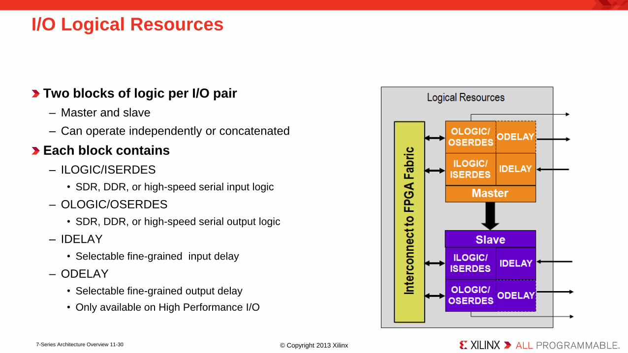
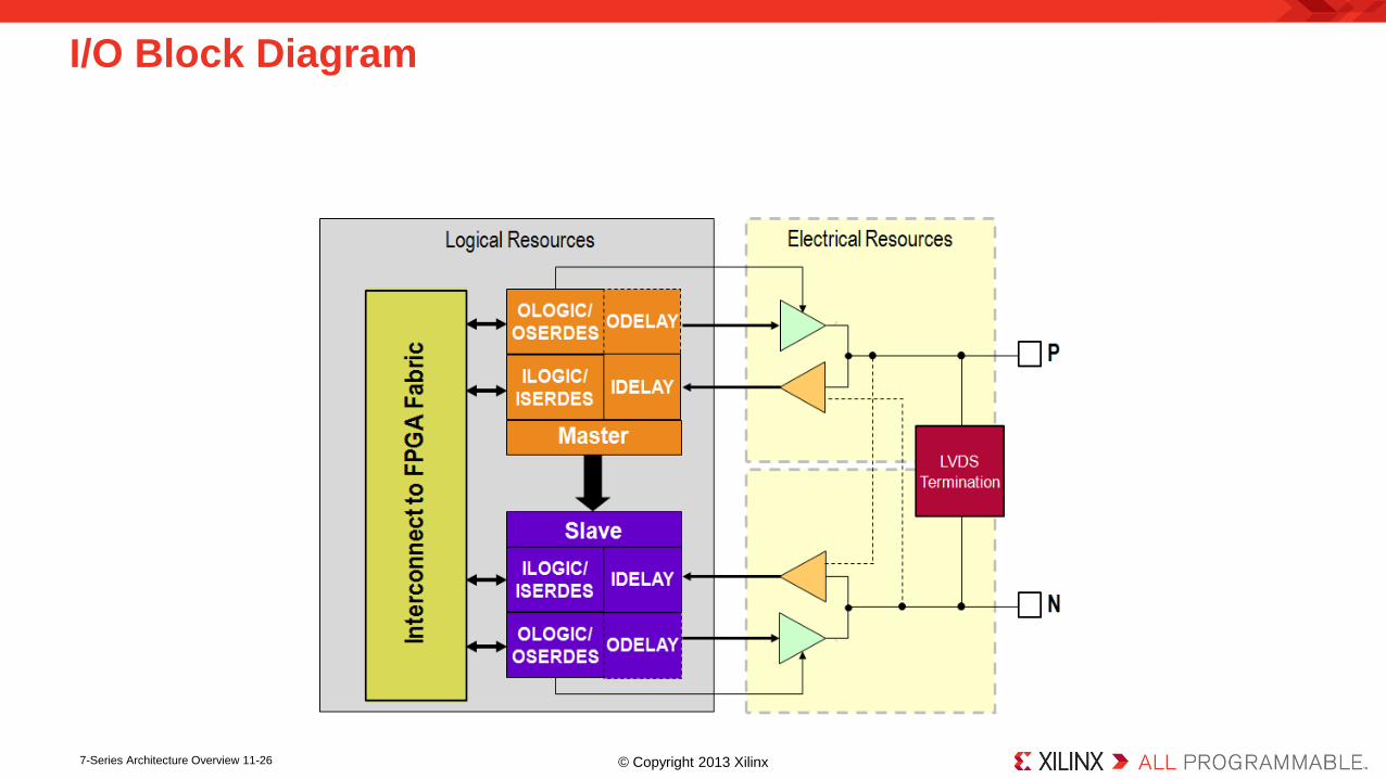
Two blocks of logic per I/O pair
– Master and slave
– Can operate independently or concatenated
Each block contains
– ILOGIC/ISERDES
• SDR, DDR, or high-speed serial input logic
– OLOGIC/OSERDES
• SDR, DDR, or high-speed serial output logic
– IDELAY
• Selectable fine-grained input delay
– ODELAY
• Selectable fine-grained output delay
• Only available on High Performance I/O
I/O Logical Resources
© Copyright 2013 Xilinx 7-Series Architecture Overview 11-30
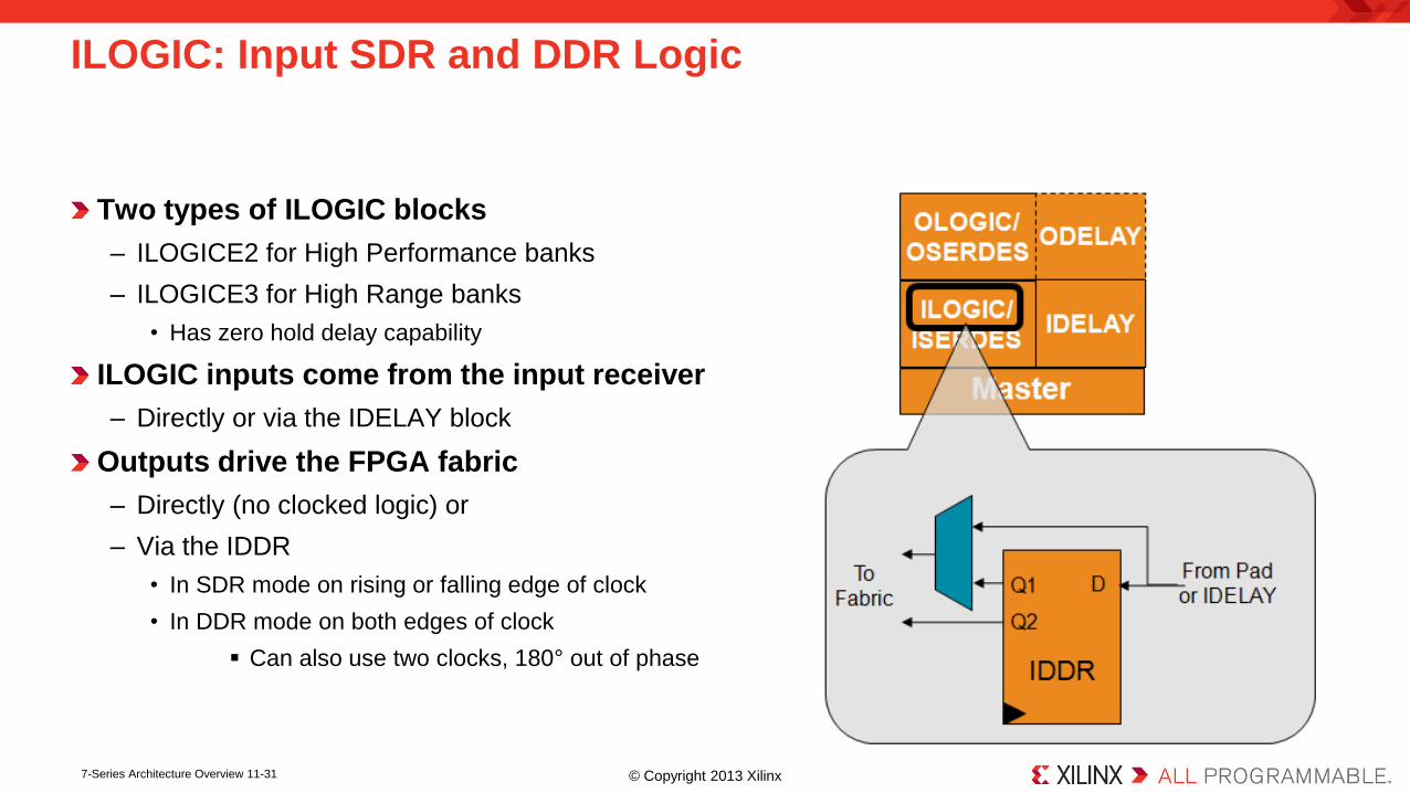
Two types of ILOGIC blocks
– ILOGICE2 for High Performance banks
– ILOGICE3 for High Range banks
• Has zero hold delay capability
ILOGIC inputs come from the input receiver
– Directly or via the IDELAY block
Outputs drive the FPGA fabric
– Directly (no clocked logic) or
– Via the IDDR
• In SDR mode on rising or falling edge of clock
• In DDR mode on both edges of clock
Can also use two clocks, 180° out of phase
ILOGIC: Input SDR and DDR Logic
© Copyright 2013 Xilinx 7-Series Architecture Overview 11-31

OLOGICE2 for HP banks, OLOGICE3 for HR
banks
Output of OLOGIC connects to the output
driver directly, or via the ODELAY
– ODELAY is available in HP banks only
Output is driven directly from the fabric
– Directly, through an SDR flip-flop or via the ODDR
using both edges of clock
Each OLOGIC block contains two ODDR
– One for controlling the data to the output driver
– One for controlling the 3-state enable
– Both ODDR are driven by same clock and reset
SAME_EDGE or OPPOSITE_EDGE only
OLOGIC: Output SDR and DDR Logic
© Copyright 2013 Xilinx 7-Series Architecture Overview 11-32

Clocks in data from input pad or IDELAY
– D is clocked on high speed clock (CLK)
– Can be SDR or DDR
Sends de-serialized data to fabric
– Q is clocked on low speed clock (CLKDIV)
CLK and CLKDIV must be in phase
De-serializes data
– Single data rate: 2, 3, 4, 5, 6, 7, 8
– Double data rate: 4, 6, 8
Cascade with slave for wider ratios
– Double data rate: 10, 14
Has BITSLIP logic for framing parallel data
ISERDES: Input Serial-to-Parallel Converter
© Copyright 2013 Xilinx 7-Series Architecture Overview 11-33

Serializes out data to output pad or ODELAY
– Q is clocked on high speed clock (CLK)
– Can be SDR or DDR
Parallel data comes from fabric
– D is synchronous to low speed clock (CLKDIV)
CLK and CLKDIV must be in phase
Serializes data
– Single data rate: 2, 3, 4, 5, 6, 7, 8
– Double data rate: 4, 6, 8
Cascade with slave for wider ratios
– Double data rate: 10, 14
When using 3-state serializer, both the data and 3-state width must be 4
– Clocks are shared between both serializers
OSERDES: Output Parallel-to-Serial Converter
© Copyright 2013 Xilinx 7-Series Architecture Overview 11-34

Separate IDELAY and ODELAY delay lines
– IDELAY is available in both HR and HP banks
– ODELAY is only available in HP banks
Delay line elements are calibrated using the IDELAYCTRL cell
– Delay is process, temperature, and voltage independent
IDELAY and ODELAY have almost identical capabilities
– IDELAY can also be accessed from the fabric
Tap counter value can be accessed via FPGA fabric
– Monitor, increment, decrement, or set the tap value; tap value can be from 0 to 31
Reference frequency can be 200 MHz in all speed grades; 300 MHz is also allowed in
fastest speed grade
– Results in 78 ps or 52 ps per tap
IDELAY and ODELAY
© Copyright 2013 Xilinx 7-Series Architecture Overview 11-35

Introduction to 7-Series FPGA
Logic Resources
I/O Resources
Memory and DSP48 Resources
XADC
Clocking Resources
Zynq FPGA
Summary
Outline
© Copyright 2013 Xilinx 7-Series Architecture Overview 11-36

All members of the 7-series families have the
same Block RAM/FIFO
Fully synchronous operation
– All operations are synchronous; all outputs are
latched
Optional internal pipeline register for higher
frequency operation
Two independent ports access common data
– Individual address, clock, write enable, clock enable
– Independent data widths for each port
7-Series Block RAM and FIFO
© Copyright 2013 Xilinx 7-Series Architecture Overview 11-37
Multiple configuration options
– True dual-port, simple dual-port, single-port
Integrated cascade logic
Byte-write enable in wider configurations
Integrated control for fast and efficient
FIFOs
Integrated 64 / 72-bit Hamming error
correction
Separate Vbram supply to ensure block
memory functionality in -1L
7-Series Block RAM and FIFO
© Copyright 2013 Xilinx 7-Series Architecture Overview 11-38
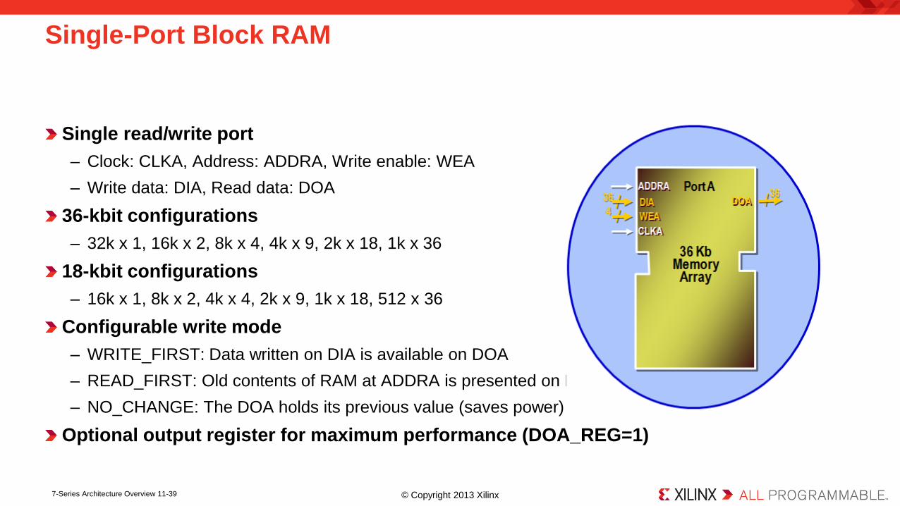
Single read/write port
– Clock: CLKA, Address: ADDRA, Write enable: WEA
– Write data: DIA, Read data: DOA
36-kbit configurations
– 32k x 1, 16k x 2, 8k x 4, 4k x 9, 2k x 18, 1k x 36
18-kbit configurations
– 16k x 1, 8k x 2, 4k x 4, 2k x 9, 1k x 18, 512 x 36
Configurable write mode
– WRITE_FIRST: Data written on DIA is available on DOA
– READ_FIRST: Old contents of RAM at ADDRA is presented on DOA
– NO_CHANGE: The DOA holds its previous value (saves power)
Optional output register for maximum performance (DOA_REG=1)
Single-Port Block RAM
© Copyright 2013 Xilinx 7-Series Architecture Overview 11-39

Two separate read/write ports
– Each port has separate clock, address, data in,
data out, write enable…
• Clocks can be asynchronous to each other
– The two ports can have different widths
• Same configurations as when single ported
– The two ports can have different write modes
No contention avoidance when both ports
access the same address, except
– If clocked by the same clock, and the write port is
READ_FIRST, the read port gets the old data
Dual-Port Block RAM
© Copyright 2013 Xilinx 7-Series Architecture Overview 11-40
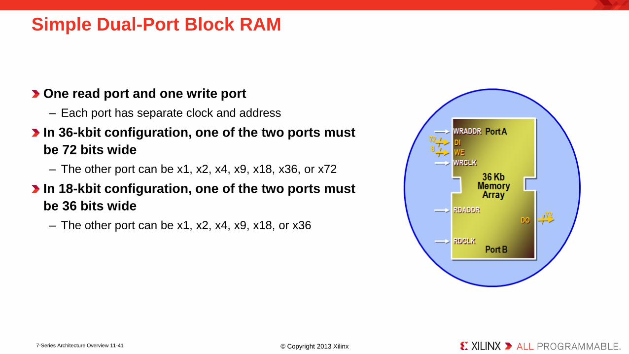
One read port and one write port
– Each port has separate clock and address
In 36-kbit configuration, one of the two ports must
be 72 bits wide
– The other port can be x1, x2, x4, x9, x18, x36, or x72
In 18-kbit configuration, one of the two ports must
be 36 bits wide
– The other port can be x1, x2, x4, x9, x18, or x36
Simple Dual-Port Block RAM
© Copyright 2013 Xilinx 7-Series Architecture Overview 11-41
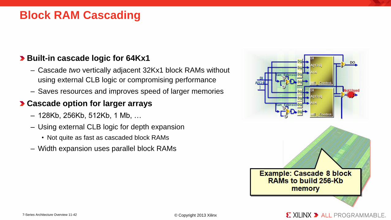
Built-in cascade logic for 64Kx1
– Cascade two vertically adjacent 32Kx1 block RAMs without
using external CLB logic or compromising performance
– Saves resources and improves speed of larger memories
Cascade option for larger arrays
– 128Kb, 256Kb, 512Kb, 1 Mb, …
– Using external CLB logic for depth expansion
• Not quite as fast as cascaded block RAMs
– Width expansion uses parallel block RAMs
Block RAM Cascading
© Copyright 2013 Xilinx 7-Series Architecture Overview 11-42

Full featured
– Synchronous or asynchronous read and write clocks
– Four flags
• Full, empty, programmable almost-full/empty
– Optional first-word-fall-through
FIFO configurations
– Any 36-Kb block RAM: 8Kx4, 4Kx9, 2Kx18, 1Kx36,
512x72
– Any 18-Kb block RAM: 4Kx4, 2Kx9, 1Kx18, 512x36
– Write and read width must be equal
Can use the integrated error correction when
used in the x72 width
FIFO
© Copyright 2013 Xilinx 7-Series Architecture Overview 11-43
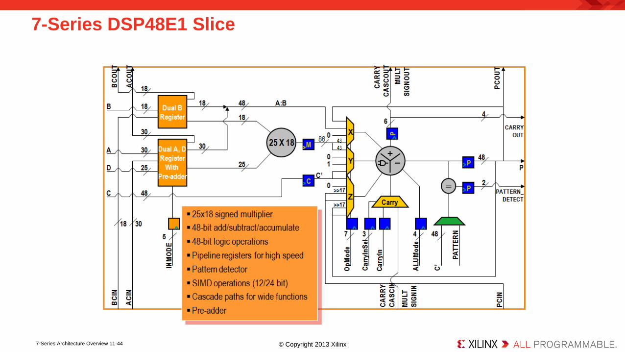
7-Series DSP48E1 Slice
© Copyright 2013 Xilinx 7-Series Architecture Overview 11-44
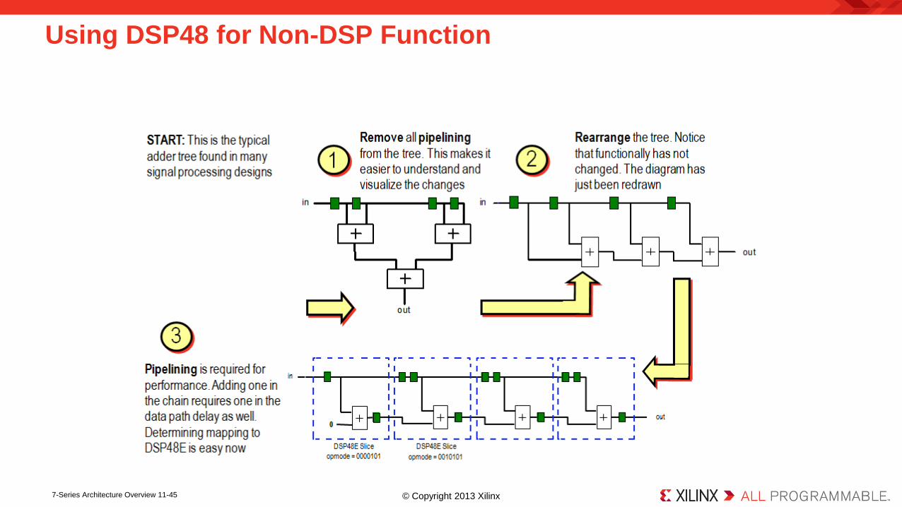
Using DSP48 for Non-DSP Function
© Copyright 2013 Xilinx 7-Series Architecture Overview 11-45
Introduction to 7-Series FPGA
Logic Resources
I/O Resources
Memory and DSP48 Resources
XADC
Clocking Resources
Zynq FPGA
Summary
Outline
© Copyright 2013 Xilinx 7-Series Architecture Overview 11-46
XADC is a high quality and flexible analog interface new to the 7-series
– Dual 12-bit 1Msps ADCs, on-chip sensors, 17 flexible analog inputs, and track & holds with
programmable signal conditioning
– 1V input range
– 16-bit resolution conversion
– Built in digital gain and offset calibration
Analog Mixed Signal (AMS)
– Using the FPGA programmable logic to customize the XADC and replace other external analog
functions; for example, linearization, calibration, filtering, and DC balancing to improve data
conversion resolution
XADC and AMS
© Copyright 2013 Xilinx 7-Series Architecture Overview 11-47
Fast sampling
– Conversion time of 1 us with support for
simultaneous sampling
– Flexible timing modes (self and externally
triggered sampling modes)
– Separate track/hold amplifier for each ADC
ensures maximum throughput using
multiplexed analog input channels
Flexible analog inputs
– Differential analog inputs with high common
mode noise rejection
– Support for unipolar, bipolar, and true
differential input signal types
XADC Block Diagram
© Copyright 2013 Xilinx 7-Series Architecture Overview 11-48
Internal and external multiplexing and sampling
– Can sample internal power supplies and temperature
– Multiplexes internal sources and 17 external analog inputs
– Can control an external analog multiplexer to reduce pin count
Flexible triggering
– Conversion data is stored in internal status registers
– Internal control registers control source selection, sampling, and alarms
– Registers can be accessed internally via the dynamic reconfiguration port (DRP)
– Register can be accessed via JTAG
• Available on power up, before configuration
Operates over a wide temperature range (–40°C to +125°C)
XADC’s Other Features
© Copyright 2013 Xilinx 7-Series Architecture Overview 11-49
Introduction to 7-Series FPGA
Logic Resources
I/O Resources
Memory and DSP48 Resources
XADC
Clocking Resources
Zynq FPGA
Summary
Outline
© Copyright 2013 Xilinx 7-Series Architecture Overview 11-50

Modern applications have complex clocking requirements
– Extremely high-performance clock signals
– Support for multiple frequency domains across a wide frequency
range
– De-skewing of clocks relative to one another
– Low jitter and precise duty cycle to maintain the widest possible
data valid window
– Lowest possible system power
Xilinx FPGAs have a rich mixture of clocking resources to
accommodate these requirements
– The perfect balance of resources at the right cost
High-Performance Clocking
© Copyright 2013 Xilinx 7-Series Architecture Overview 11-51

Systems usually require multiple clock
frequencies from the same source
– Minimizing the number of oscillators lowers
system cost
External clock sources can often be noisy
– Filtering jitter cleans up clocks widening the data
valid window
Many circuits need to be clocked at the
same time to ensure correct operation
– De-skewing and aligning clocks eliminates hold-
time issues and race conditions
Clock Management
© Copyright 2013 Xilinx 7-Series Architecture Overview 11-52

Global clock buffers
– High fanout clock distribution buffer
Low-skew clock distribution
– Regional clock routing
Clock regions
– Each clock region is 50 CLBs high and spans half the device
Clock management tile (CMT)
– One Mixed-Mode Clock Managers (MMCMs) and one Phase
Locked Loop (PLL) in each Clock
– Performs frequency synthesis, clock de-skew, and jitter-
filtering
– High input frequency range
Simple design creation through the Clocking Wizard
7-Series FPGAs Clock Management
© Copyright 2013 Xilinx 7-Series Architecture Overview 11-53

All synchronous designs need at least one external clock reference
– Many designs require several clock sources
These sources need to be brought into the FPGA and connected to the internal FPGA
clock resources
Every 7-series FPGA has four clock-capable inputs in each bank
– These inputs are regular I/O pins with dedicated connections to internal clock resources
• When not used as clock inputs, they can be used as a regular I/O pin
– Each clock input can be used as a single-ended clock input, or can be paired with an adjacent pin to
form a differential clock input
• Each bank can therefore have four single-ended or four differential clock inputs
– Two of the four are Multi-Region Clock Capable (MRCC) and the other two are Single Region Clock
Capable (SRCC)
Clock-Capable Inputs
© Copyright 2013 Xilinx 7-Series Architecture Overview 11-54
An FPGA is a regular array of resources
– Many of these resources require clocks for synchronous operations
• Slice flip-flops, input/output flip-flops, block RAMs, DSP slices
– In order to implement synchronous designs, clocks must be distributed to these clocked elements
For synchronous operation, clocks must arrive at the clocked elements with
– Extremely low clock skew: Ensures minimal internal hold-time issues
– Low clock jitter: Allows for highest performance
– Duty cycle preservation: Important for Double Data Rate (DDR) applications
– Low insertion latency: Important for synchronous input and output interfaces
See next slide for the die
Clock Networks
© Copyright 2013 Xilinx 7-Series Architecture Overview 11-55
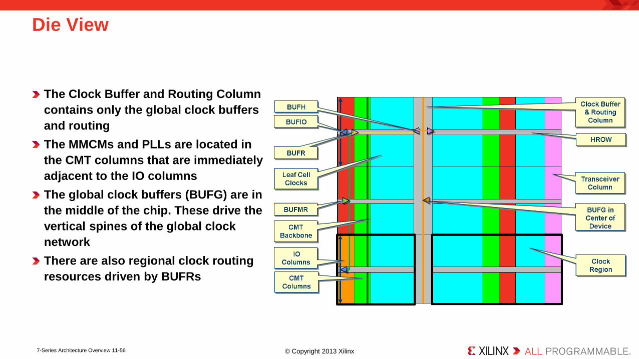
The Clock Buffer and Routing Column
contains only the global clock buffers
and routing
The MMCMs and PLLs are located in
the CMT columns that are immediately
adjacent to the IO columns
The global clock buffers (BUFG) are in
the middle of the chip. These drive the
vertical spines of the global clock
network
There are also regional clock routing
resources driven by BUFRs
Die View
© Copyright 2013 Xilinx 7-Series Architecture Overview 11-56

The horizontal spines of the global
clock network run through the center
of each clock region. These horizontal
spines are driven by BUFH buffers
Clocks are driven up and down from
the center horizontal row (HROW) of
each clock region
The BUFIO are placed within the I/O
column, and drive the I/O clock
network in that bank
The BUFMR are dedicated buffers that
allow clock inputs to drive the BUFIOs
and BUFRs of adjacent regions
Die View
© Copyright 2013 Xilinx 7-Series Architecture Overview 11-57
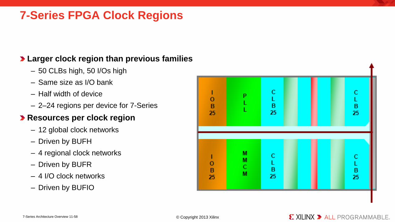
Larger clock region than previous families
– 50 CLBs high, 50 I/Os high
– Same size as I/O bank
– Half width of device
– 2–24 regions per device for 7-Series
Resources per clock region
– 12 global clock networks
– Driven by BUFH
– 4 regional clock networks
– Driven by BUFR
– 4 I/O clock networks
– Driven by BUFIO
7-Series FPGA Clock Regions
© Copyright 2013 Xilinx 7-Series Architecture Overview 11-58

BUFGCTRLs (or BUFG) reside in the center of the device
BUFGCTRLs can be driven by
– Clock-capable I/O (CCIO) in the same half
– CMT outputs in the same half
– Gigabit transceiver clocks in the same half
– Other BUFG, interconnect, or BUFR
BUFGCTRL outputs drive the vertical global clock spine
BUFGCTRL component implements
– Simple clock buffer (BUFG)
– Clock buffer with clock switching (BUFGMUX or BUFGMUX_CTRL)
– Clock buffer with clock enable (BUFGCE)
Global Clock Buffer (BUFGCTRL)
© Copyright 2013 Xilinx 7-Series Architecture Overview 11-59

Introduction to 7-Series FPGA
Logic Resources
I/O Resources
Memory and DSP48 Resources
XADC
Clocking Resources
Zynq FPGA
Summary
Outline
© Copyright 2013 Xilinx 7-Series Architecture Overview 11-60
Complete ARM®-based processing system
– Application Processor Unit (APU)
• Dual ARM Cortex™-A9 processors
• Caches and support blocks
– Fully integrated memory controllers
– I/O peripherals
Tightly integrated programmable logic
– Used to extend the processing system
– Scalable density and performance
Flexible array of I/O
– Wide range of external multi-standard I/O
– High-performance integrated serial transceivers
– Analog-to-digital converter inputs
Zynq-7000 Family Highlights
© Copyright 2013 Xilinx 7-Series Architecture Overview 11-61

The Zynq-7000 AP SoC architecture consists of two major sections
– PS: Processing system
• Dual ARM Cortex-A9 processor based
• Multiple peripherals
• Hard silicon core
– PL: Programmable logic
• Shares the same 7-series programmable logic as
Artix™-based devices: Z-7010 and Z-7020 (high-range I/O banks only)
Kintex™-based devices: Z-7030 and Z-7045 (mix of high-range and high-performance I/O banks)
The PS and the PL
© Copyright 2013 Xilinx 7-Series Architecture Overview 11-62
Introduction to 7-Series FPGA
Logic Resources
I/O Resources
Memory and DSP48 Resources
Clocking Resources
Zynq FPGA
Summary
Outline
© Copyright 2013 Xilinx 7-Series Architecture Overview 11-63
The 7-series FPGA slices contain four 6-input LUTs, eight registers, and carry logic
– LUTs can perform any combinatorial function of up to six inputs
– LUTs are connected with dedicated multiplexers and carry logic
– Some LUTs can be configured as shift registers or memories
– Slices also contain carry logic and the MUXF7 and MUXF8 multiplexers
– The MUXF7 multiplexers combine LUT outputs to create 7-input functions or 8-input multiplexers
– The MUXF8 multiplexers combine the MUXF7 outputs to create 8-input functions or 16-input
multiplexers
– The carry logic can be used to implement fast addition, subtraction, and comparison operations
The 7-series FPGA IOBs contain DDR registers as well as SERDES resources
The SelectIO™ interfaces enable direct connection to multiple I/O standards
Summary
© Copyright 2013 Xilinx 7-Series Architecture Overview 11-64
The 7-series FPGA includes dedicated block RAM and DSP slice resources
The 7-series FPGAs includes dedicated MMCMs, PLLs, and routing resources to
improve your system clock performance and generation capability
The 7-series FPGAs include other dedicated hardware such as XADC
The Zynq-7000 processing platform is a system on a chip (SoC) processor with
embedded programmable logic fabric of either Artix or Kintex 7-series FPGA
Summary
© Copyright 2013 Xilinx 7-Series Architecture Overview 11-65