7. Application II - Porous alumina photonic crystals
12
7. Application II - Porous alumina photonic crystals Periodic dielectric materials allowing to control the flow of light are classified as photonic crys- tals (PCs) [135]. Numerous publications have already been dedicated to realize this concept with various materials. For example, PCs based on silicon are of great interest since they can be easily integrated into the already existing modern VLSI systems [7, 136]. Also, opal structures formed by self-assembly have been intensively exploited because of the potential to fabricate three-dimensional PCs [137, 138, 139]. 7.1 Definition of photonic bandgaps The definition of the photonic bandgaps is borrowed from that of the bandgaps in solid-state physics. For example, in a crystal, the interaction between the periodically arranged atoms and electrons moving through this lattice results in the formation of allowed and forbidden energy states, determining the properties of crystals. Similarly, we can consider photons moving through transparent dielectric material with a peri- odic potential. If absorption of the light by the material is negligible and the contrast in refrac- tive index between the two regions is high enough, light can not propagate in certain directions with specified energies due to the photonic band gap. The photonic band gaps are determined by the configuration (geometry and spacing) of air holes and the contrast in refractive index. The size of photonic bandgap is determined by the refractive index contrast and by the filling ratio 1 of the higher-index material [140]. The location of the gap is determined by the lattice constant. For example, the wavelength of light in photonic band gaps can be roughly estimated by the spacing between the air holes (or the lattice size) times the sum of refractive index of the dielectric materials (λ gap ∼ 2(n 1 × D p + n 2 × D Alox )) [135]. 7.2 Porous alumina photonic crystals Due to their low absorption coefficient, excellent thermal stability and easy handling, porous alumina structures could be potential materials for PCs in the visible and infrared. The elec- tronic bandgap of alumina is 7 ∼ 9.5 eV. Up to now, there have been no detailed studies in terms of real porous alumina structures of two layers: an inner layer consisting of a high purity alumina, an outer layer of alumina incorporated with anions, for example, PO 3- 4 (see the Chapters 1 and 2) [24, 41, 141]. 1 = Pore radius (r)/Interpore distance (D int ) 71
Transcript of 7. Application II - Porous alumina photonic crystals

7. Application II - Porous aluminaphotonic crystals
Periodic dielectric materials allowing to control the flow of light are classified as photonic crys-tals (PCs) [135]. Numerous publications have already been dedicated to realize this conceptwith various materials. For example, PCs based on silicon are of great interest since they can beeasily integrated into the already existing modern VLSI systems [7, 136]. Also, opal structuresformed by self-assembly have been intensively exploited because of the potential to fabricatethree-dimensional PCs [137, 138, 139].
7.1 Definition of photonic bandgaps
The definition of the photonic bandgaps is borrowed from that of the bandgaps in solid-statephysics. For example, in a crystal, the interaction between the periodically arranged atoms andelectrons moving through this lattice results in the formation of allowed and forbidden energystates, determining the properties of crystals.
Similarly, we can consider photons moving through transparent dielectric material with a peri-odic potential. If absorption of the light by the material is negligible and the contrast in refrac-tive index between the two regions is high enough, light can not propagate in certain directionswith specified energies due to the photonic band gap.
The photonic band gaps are determined by the configuration (geometry and spacing) of air holesand the contrast in refractive index. The size of photonic bandgap is determined by the refractiveindex contrast and by the filling ratio1 of the higher-index material [140]. The location of thegap is determined by the lattice constant. For example, the wavelength of light in photonic bandgaps can be roughly estimated by the spacing between the air holes (or the lattice size) timesthe sum of refractive index of the dielectric materials (λgap ∼ 2(n1 ×Dp + n2 ×DAlox)) [135].
7.2 Porous alumina photonic crystals
Due to their low absorption coefficient, excellent thermal stability and easy handling, porousalumina structures could be potential materials for PCs in the visible and infrared. The elec-tronic bandgap of alumina is 7∼ 9.5 eV.
Up to now, there have been no detailed studies in terms of real porous alumina structures of twolayers: an inner layer consisting of a high purity alumina, an outer layer of alumina incorporatedwith anions, for example, PO3−4 (see the Chapters 1 and 2) [24, 41, 141].
1 = Pore radius (r)/Interpore distance (Dint)
71

In this chapter, we will discuss in detail large-area PCs based on porous alumina. The measuredreflectivity will be compared with theoretical predictions. Moreover, a distribution of anions inthe duplex oxide layers of the porous alumina wall to explain the optical properties is suggested.
7.2.1 Optical characterization of porous alumina
Γ
Mk
Mk Γ
a b
Figure 7.1: Hexagonal lattice (a) in real lattice space; (b) in reciprocal space. The high-symmetrydirectionsΓ−M andΓ− k are indicated.
Before optical characterization, porous alumina membranes are prepared by selective etchingof aluminum in a CuCl2-containing solution. Afterwards, the membranes are cleaved mechan-ically and good cleaved planes are confirmed by SEM. For the optical characterization, thereflectivity of the porous alumina structures with differentr/Dint-values are measured alongΓ−M direction (see Fig. 7.1) with Fourier Transform InfraRed (FT-IR) Spectrometer (Bruker,IFS 66) equipped with a UV-CaF2-beamsplitter, a tungsten lamp, and a MCT detector.2
7.2.2 Optical setup Beamsplitter
Source
Mirror2
Mirror1
(1)
(2)
(3)
(4)
Probe
Detector
xFigure 7.2: The Michelson interferometer.
2(HgCdTe) photoconductive detector. This fast detector is suitable for measuring the infrared radiation.
72
The underlying principle of the reflectivity measurement with the FT-IR microscope is based ona Michelson interferometer and Casse - grain method. The Michelson interferometer consists ofa beamsplitter, a fixed mirror (Mirror 1), and a translatable mirror (Mirror 2) (see Fig. 7.2). Thebeam radiated from the source (beam 1) is separated into two beams by the beamsplitter: halfof the radiation is reflected to the fixed mirror (beam 2) and the other half is transmitted to themoving mirror (beam 3). The fixed and moving mirrors reflect the beams back to the beamsplit-ter. Again, half of this reflected beams is transmitted and half is reflected at the beamsplitter,resulting in one beam passing to the detector (beam 4) and the second back to the source.
The optical path difference (∆), which is defined as the difference between the beams travellingthrough the fixed and moving mirrors, is
∆p = 2 x n cos(δ) (7.1)
Wherex is the moving mirror displacement,n is the index of refraction of the medium fillingthe interferometer arms,δ is the angle of the inclination of the beam relative to the optical axis.For a normal beam (cos(δ) = 1) and for the air medium (n = 1),∆p = 2 x. The net optical pathdifference is∆ = ∆p + ∆r, where the equivalent path difference arising from phase change onreflection,∆r, is π due to two external reflections in the case of beam 2, whereas only one forbeam 3.3 If ∆ = mλ or = (m + 1
2)λ, constructive or destructive interference of the two beams
is produced, respectively, for everyλ/2 translation of one of the mirrors [142].
An interferogram4 of a signal is collected as a function of the optical path difference. Afterward,the spectrum is obtained by performing a Fourier Transform (FT) on the interferogram as afunction of wavelength. The measurement with the FT-IR spectroscopy is performed twicewith and without the sample present. The signal originating from the sample is calculated fromthe difference between the two computed spectra.
To measure the reflectivity of the sample, the Casse - grain method is employed as shown inFig. 7.3. The angular apertures of the IR-objective is 30◦ (see Fig. 7.3).
A background measurement is performed on a silver mirror as a reference prior to the actualmeasurements.
7.2.3 Calculations of reflectivity and bandstructure
Bandstructures of the porous alumina PCs are calculated with the MIT package [143]. In addi-tion, numerical calculations of reflectivity are performed by the transfer-matrix method [144].The theoretical predictions are compared to the experimental results.
7.2.4 Duplex structure of porous alumina: inner and outer oxide
Fig. 3.7 shows monodomain porous alumina with 500 nm interpore distance and 100µm inlength. The structure shows a defect-free array and straight channels. It should be suitable asPCs.
Details of porous alumina structures are very similar to those shown in Fig. 2.1 [41]. Fig.7.4 reveals that the inner oxide layer near the cell boundary is about 50 nm thick. The outer
3A relative phase shift ofπ occurs by reflection of the light going from a lower index toward a high index,so-called the external reflection.
4The name of the signal format acquired by an FT-IR spectrometer.
73

Probe
30°Parabolic Mirrors
Slit
From FI-IR To detector
Figure 7.3: Casse - grain mirror objective in theFT-IR microscope.
Figure 7.4: TEM image of a porous alu-mina array obtained by imprint lithogra-phy and subsequent anodization (195V,1 wt% H3PO4). The duplex oxide lay-ers consist of an inner oxide and an outeroxide are visible. The thickness of theinner oxide is 50 nm, whereas that of theouter oxide decreases with increasing thepore diameter (initial diameter : 180 nm)by isotropic etching.
74
oxide layer is between the inner oxide layer and the air pore. As already discussed, the inneroxide layer is known to be composed of pure aluminum oxide, whereas the outer oxide layerhas impurities such as incorporated anions [141]. The nomenclature of the inner oxide and theouter oxide was discussed in the Section 1.4.1.
It is reasonable to assume that phosphorus (P) and water (H2O) are major impurities sinceH3PO4 is used as the electrolyte. Previous studies revealed that in the case of barrier oxideformation in phosphate solution, phosphorus in the form of PO3−
4 exists in the outer part andsome protons are incorporated in the oxide at the electrolyte/oxide interface [145].
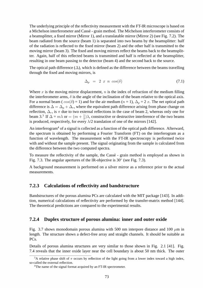
a
b Figure 7.5: SEM micrograph of a cross-section of porous alumina formed underthe same conditions of Fig. 3.7 and Fig.7.4. The barrier oxide layer, the inneroxide, the outer oxide and the pore areclearly distinguishable. The interporedistanceDint is 500 nm. The arrows la-belled asa andb indicate the thicknessesof the barrier layer and the wall, respec-tively.
The duplex layers of inner and outer oxides exist not only in the wall but also in the barrier layerat the pore bottoms (Fig. 7.5). The thickness of the outer oxide layer in the barrier is exactlythe same as that in the wall. However, the inner oxide layer in the center of the hemisphere ofthe barrier layer is twice as thick as that in the wall, while the inner oxide at the edge of thehemisphere is the same thickness as that in the wall. This observation could be explained by thefact that maximum electric field is concentrated at the pore center [26].
7.2.5 Optical characterization
The reflectivity of porous alumina with different values of ther/Dint-ratio is measured alongtheΓ - M direction by an FT-IR equipped with a microscope. The measurement is carried outon a plane parallel to the long axes of the pores. The samples are prepared by carefully cleavingthem. As described in the previous section, the porous alumina structures have duplex oxidelayers with different dielectric constants. As a result, the effective dielectric constant of thewhole structure is not constant for different values ofr/Dint-ratio. In particular, we will seelater that the outer oxide layer has a non-homogeneous effective dielectric constant dependingon the concentration of impurities at different point.
As indicated previously [41], for the lattice constantDint = 500 nm, the porous alumina struc-ture is only composed of the inner oxide layer when the pore radiusr ≥ 200 nm. Therefore, thereflectivity of a sample withr/Dint = 0.4, which is composed of only inner oxide, is measuredfirst. Note that pores are hexagonal and not round for this pore radius.
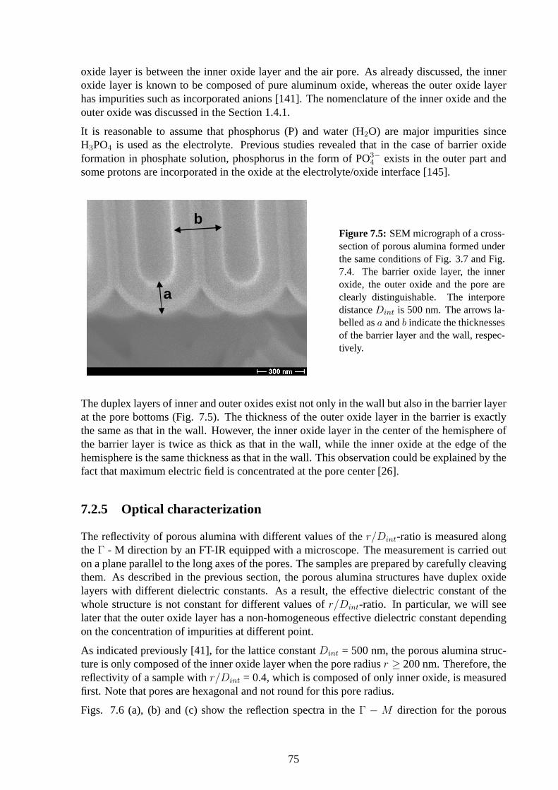
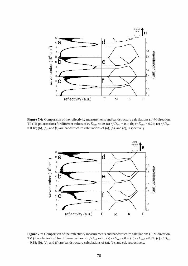
Figs. 7.6 (a), (b) and (c) show the reflection spectra in theΓ − M direction for the porous
75
6
8
10
12
2.52
1.5
1
2.52
1.5
1
6
8
10
12
2.52
1.5
1
4
6
8
10
12
H
ΚΜ ΓΓ
wav
enum
ber (
103 c
m-1)
reflectivity (a.u.)
wavelength(µm
)
Figure 7.6: Comparison of the reflectivity measurements and bandstructure calculations (Γ-M direction,TE (H)-polarization) for different values ofr/Dint ratio: (a)r/Dint = 0.4; (b)r/Dint = 0.24; (c)r/Dint
= 0.18; (b), (e), and (f) are bandstructure calculations of (a), (b), and (c), respectively.
2.52
1.5
1
6
8
10
12
2.52
1.5
1
6
8
10
12
2.52
1.5
1
4
6
8
10
12
E
ΚΜ ΓΓ
reflectivity (a.u.)
wav
enum
ber (
103 c
m-1)
wavelength(µm
)
Figure 7.7: Comparison of the reflectivity measurements and bandstructure calculations (Γ-M direction,TM (E)-polarization) for different values ofr/Dint ratio: (a)r/Dint = 0.4; (b)r/Dint = 0.24; (c)r/Dint
= 0.18; (b), (e), and (f) are bandstructure calculations of (a), (b), and (c), respectively.
76
alumina withr/Dint = 0.4, 0.24 and 0.18, respectively. The stopgaps5 of TE polarization inΓ −M direction for these threer/Dint ratios are 0.96µm - 1.20µm, 1.17µm - 1.36µm and1.28µm - 1.41µm, respectively. Fig. 7.7 shows that stopgaps of the TM polarization exist onlyin theΓ−M direction for allr/Dint ratios.
Table 7.1: Literature survey of refractive index,n, of alumina. Here, we assume that the dielectricconstant of alumina,ε, is equivalent ton2 due to a low absorption coefficient in the visible and infraredranges.
Authors Refractive indexn conditionsK. Huber [146] 1.65 unknownG. Hass [147] 1.67 - 1.62 @λ = 0.3 - 0.6µm 3% Ammonium tartrate
S. Nakamuraet al. [148] 1.64 @λ = 0.546µm 4.25% Phosphoric acid (140 V)
For both polarizations, the dielectric constant of the inner oxide is deduced by the position andwidth of the maximum reflection (photonic stopgap inΓ−M direction) compared to the theo-retical calculation for different values of refractive indices. The dielectric constant of the inneroxide,εinner, is determined by the bandstructure calculation which matches best the measuredreflection in the porous alumina withr/Dint = 0.4. Here,εinner is estimated around 2.8 (corre-sponding ton = 1.67) for both E- and H- polarization, which is in a good agreement with thepreviously reported dielectric constant of pure aluminum oxide (Table 7.1). Note that amongthe three dispersion relations (Fig. 7.6 (d), (e) and (f)) for TE mode, a bandgap in all directionis opened forr/Dint = 0.40 andr/Dint = 0.24. The dispersion relation forr/Dint = 0.18 doesnot open a bandgap in all directions, but a stopgap in theΓ−M direction.
0.0
0.2
0.4
0.6
0.8
1.0
0 4 8 12 16 20
0.0
0.2
0.4
0.6
0.8
1.0
0 4 8 12 16 20
0.0 0.2 0.4 0.6 0.8 1.0
Wavenumber (103cm-1)
Frequency (ωa/2πc)
b a
Wavenumber (103cm-1)
Ref
lect
ivity
0.0 0.2 0.4 0.6 0.8 1.0Frequency (ωa/2πc)
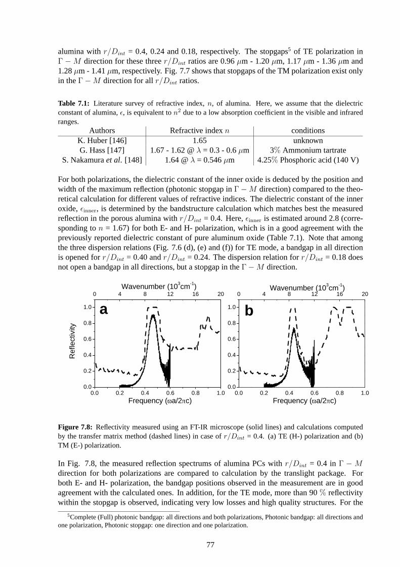
Figure 7.8: Reflectivity measured using an FT-IR microscope (solid lines) and calculations computedby the transfer matrix method (dashed lines) in case ofr/Dint = 0.4. (a) TE (H-) polarization and (b)TM (E-) polarization.
In Fig. 7.8, the measured reflection spectrums of alumina PCs withr/Dint = 0.4 in Γ − Mdirection for both polarizations are compared to calculation by the translight package. Forboth E- and H- polarization, the bandgap positions observed in the measurement are in goodagreement with the calculated ones. In addition, for the TE mode, more than 90% reflectivitywithin the stopgap is observed, indicating very low losses and high quality structures. For the
5Complete (Full) photonic bandgap: all directions and both polarizations, Photonic bandgap: all directions andone polarization, Photonic stopgap: one direction and one polarization.
77
TM mode, a slight blue shift on the high frequency side implies a stronger angular dependenceof the E-polarization since the IR-objective has an angular aperture of 30◦ (see Fig. 7.3).
a b
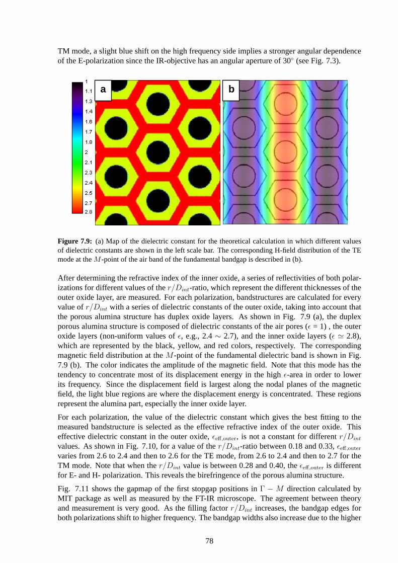
Figure 7.9: (a) Map of the dielectric constant for the theoretical calculation in which different valuesof dielectric constants are shown in the left scale bar. The corresponding H-field distribution of the TEmode at theM -point of the air band of the fundamental bandgap is described in (b).
After determining the refractive index of the inner oxide, a series of reflectivities of both polar-izations for different values of ther/Dint-ratio, which represent the different thicknesses of theouter oxide layer, are measured. For each polarization, bandstructures are calculated for everyvalue ofr/Dint with a series of dielectric constants of the outer oxide, taking into account thatthe porous alumina structure has duplex oxide layers. As shown in Fig. 7.9 (a), the duplexporous alumina structure is composed of dielectric constants of the air pores (ε = 1) , the outeroxide layers (non-uniform values ofε, e.g., 2.4∼ 2.7), and the inner oxide layers (ε ' 2.8),which are represented by the black, yellow, and red colors, respectively. The correspondingmagnetic field distribution at theM -point of the fundamental dielectric band is shown in Fig.7.9 (b). The color indicates the amplitude of the magnetic field. Note that this mode has thetendency to concentrate most of its displacement energy in the highε-area in order to lowerits frequency. Since the displacement field is largest along the nodal planes of the magneticfield, the light blue regions are where the displacement energy is concentrated. These regionsrepresent the alumina part, especially the inner oxide layer.
For each polarization, the value of the dielectric constant which gives the best fitting to themeasured bandstructure is selected as the effective refractive index of the outer oxide. Thiseffective dielectric constant in the outer oxide,εeff,outer, is not a constant for differentr/Dint
values. As shown in Fig. 7.10, for a value of ther/Dint-ratio between 0.18 and 0.33,εeff,outer
varies from 2.6 to 2.4 and then to 2.6 for the TE mode, from 2.6 to 2.4 and then to 2.7 for theTM mode. Note that when ther/Dint value is between 0.28 and 0.40, theεeff,outer is differentfor E- and H- polarization. This reveals the birefringence of the porous alumina structure.
Fig. 7.11 shows the gapmap of the first stopgap positions inΓ − M direction calculated byMIT package as well as measured by the FT-IR microscope. The agreement between theoryand measurement is very good. As the filling factorr/Dint increases, the bandgap edges forboth polarizations shift to higher frequency. The bandgap widths also increase due to the higher
78

0.20 0.25 0.30 0.35 0.40
2.4
2.5
2.6
2.7
2.8
of o
uter
oxi
de
ε
r/a (pore radius/interpore distance)
Figure 7.10: Effective dielectric con-stant of the outer oxide as a function ofthe r/Dint value (? : TE mode and•:TM mode). Note that the points wherer/Dint = 0.4 represent the dielectric con-stant of the inner oxide.
0.30
0.35
0.40
0.45
0.50
6
7
8
9
10
0.20 0.25 0.30 0.35 0.400.30
0.35
0.40
0.45
0.50
6
7
8
9
10
Wav
enum
ber (
103 cm
-1)
Filling ratio r/a
Freq
uenc
y (ω
a/2π
c)
b
a
Figure 7.11: Map of stopgaps as a func-tion of the filling ratio r/Dint. (a)The TE-mode: Stars (?) indicate stopgapfrom the reflectivity measurements inΓ-M direction. Dashed lines correspondto theoretical calculations of the stopgap.The hatched area indicates the calculatedphotonic bandgap in all in-plane direc-tions which is deduced from bandstruc-ture calculations. (b) The TM-mode:Dots (•) represent the stopgap from thereflectivity measurements inΓ-M direc-tion. The calculated stopgap is shown insolid lines. Note that there is no photonicbandgap in all in-plane directions for theTM mode due to the low dielectric con-stant contrast.
79

dielectric contrast of the whole structure. In the figure 7.11 (a), the hatched area shows thecalculated photonic bandgap frequency range for the TE mode. The maximum gap-midgapratio6 is 9.73% for r/Dint = 0.40. The bandgap frequencies are higher compared to the resultsin reference [7]. This is due to the facts that the real structure of the porous alumina consistsof the duplex oxide layers and that the interface between the two oxide layers has a hexagonalshape.
In fact, Masudaet al. reported that stopgaps for both polarizations in the porous alumina PCswith r/Dint = 0.18 are observed, which are in a good agreement with theoretical predictionsassuming a dielectric constant of 2.8 [150]. Note that if we take 2.8 as dielectric constant of theinner oxide and 2.6 as dielectric constant of the outer oxide, the effective dielectric constant ofthe whole oxide structure is only slightly lower than the value used by Masudaet al. [150].
7.2.6 Discussion
Figure 7.12: Schematic diagram ofporous alumina oxide layers consistingof inner oxide and outer oxide. Anions(black points) are enriched in the inter-mediate part of the outer oxide. Note thatthe inner oxide in the center of the hemi-spheric scallop of barrier layer is twice aslarge as that in the edge of hemisphericscallop of the barrier layer or in the wall.
In this section, the reason for the distribution of the effective dielectric constant in the outeroxide layer will be discussed.
The inhomogeneities of the dielectric constant within the outer oxide layer might be explainedby the nonuniform distribution of anions in the outer oxide layer. Several possible aluminaminerals with different refractive indices could be considered as shown in Table 7.2.
Compared to the dielectric constant of the pure alumina, the anion-incorporated alumina min-erals have lower dielectric constants. The more anions are incorporated in the alumina, thelower the dielectric constant. In addition, as the degree of hydrates in the minerals decreasesfrom tri- to mono-, the corresponding refractive index increases. The density of the materi-als is increased in a similar way, so that the change in the effective dielectric constant can beattributed to a density modification. For example, for both augelite and wavellite containingphosphorus, the refractive index is similar to or smaller than that in hydrated alumina oxides. Itis reasonable to assume that anion complexes containing phosphorous are concentrated in theintermediate part (Fig. 7.12). This region corresponds to the minimum dielectric constant inFig. 7.10. As the anion-contamination decreases towards the inner oxide layer and the outer-most oxide layer, the effective dielectric constant for both regions increases. This interpretation
6It is the ratio of∆ωω0
, where∆ω = ωc - ωv. ωv andωc are the lower and upper band edge frequencies of thegap, respectively.ω0 is the midgap frequency. This parameter is dimensionless, not depending on the scale of thephotonic cystal [149].
80

Table 7.2: Possible alumina minerals with the different refractive indices [70].nα, nβ , andnγ are thethree coordinate axes in the order of least, intermediate, and greatest index.
Name composition Refractive index Density(g/cm3)Wavellite Al 3(OH)3(PO4)2·5H2O nα=1.527 2.36
nβ=1.535nγ=1.553
Augelite Al 2(PO4)(OH)3 nα=1.574 2.70nβ=1.576nγ=1.588
Gibbsite α-Al(OH)3 nα=1.57 2.42nβ=1.57nγ=1.59
Diaspore β-AlO(OH) nα=1.694 3.4nβ=1.715nγ=1.741
Boehmite α-AlO(OH) nα=1.64 3.44nβ=1.65nγ=1.66
Corundum α-Al 2O3 nα=1.761 3.97nβ=1.769
is in line with a model for the porous alumina structure suggested by Fukuda and Takahashiet al. [151, 152, 153, 154]. According to their model, the pore wall of porous alumina con-sists of an inner oxide layer composed of pure alumina and an outer oxide layer. The outeroxide layer again consists of an outermost oxide part and an intermediate oxide part. Takahashiet al. claim that the mobility of PO3−4 is responsible for the nonuniform anion concentration[151, 152, 153]. Adsorbed anions, for example, PO3−
4 , OH− and O2−, are pulled into the neg-atively charged electrode by the electric field. Since the size of the phosphorus anion complexis larger than the size of the other anions, the adsorbed PO3−
4 migrates more slowly comparedwith OH− and O2−. The phosphorus anion complex is delayed in the intermediate part sincethe attracting force in the intermediate part is weaker than that in electrolyte/outermost oxideinterface. As a result, PO3−4 is concentrated in the intermediate part of the outer wall.
7.3 Summary
Porous alumina PCs with different values ofr/Dint-ratio were fabricated via nanoindentationand subsequent anodization. The porous alumina structures consisted of an inner oxide layerof pure alumina with 50 nm thickness and an outer oxide layer containing impurities such asincorporated anions.
The reflectivity of the porous alumina PCs with the series ofr/Dint ratios (0.18∼ 0.40) wasmeasured and compared with the corresponding bandstructure calculations. Even though com-plete photonic bandgaps were not observed due to the low dielectric contrast, photonic stopgapsin both TE-and TM-polarizations in theΓ - M direction were detected in near-infrared regime.In addition, comparison of theory with experiment showed that the outer oxide layer has anon-homogenous dielectric constant depending on the degree of impurity concentration. Forexample, theεeff,outer varies from 2.6 forr/Dint = 0.18, to 2.4 forr/Dint = 0.22, and to 2.7 for
81

r/Dint = 0.33 for the TM mode. It can be concluded that the outer oxide layer consists again ofan outermost part and an intermediate part. It was suggested that the phosphorous anion com-plexes incorporated in the outer oxide layer are enriched in the intermediate part of the outeroxide layer.
82


![Inorganic Photonic Microspheres with Localized Concentric ......multifunctional zinc oxide and alumina are used as building materials of PC shell,[30] and are chemically grown onto](https://static.fdocuments.in/doc/165x107/60e68a6e1b271a24485fd9cc/inorganic-photonic-microspheres-with-localized-concentric-multifunctional.jpg)