Porous silicon and Si nanoparticles: new photonic and...
43
Porous silicon and Si nanoparticles: new photonic and electronic materials Technologies and physics properties проф. В.А.Скришевський
Transcript of Porous silicon and Si nanoparticles: new photonic and...
Porous silicon and Si nanoparticles:
new photonic and electronic materials
Technologies and physics properties
проф. В.А.Скришевський
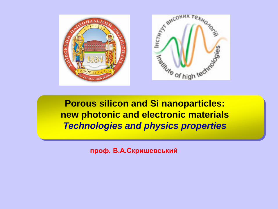
OUTLINE
Technology of nano- and Porous Si
Electrical
properties
Wave-
guides,
optical
fibers,
filters,
mirrors
Surface Optical
properties
Photonic
crystals
Chemical &
bio-sensors
Medicine:
Implants,
Diagnostics
electrophoresis,
drug deliver Solar
Cells
Bioreactors,
syntesis
LED, Microelectronics:
SOI, Si epitaxy
Hydrogen
reservoirs
Explosive
materials
Luminescence
Applications
1
2
3
4
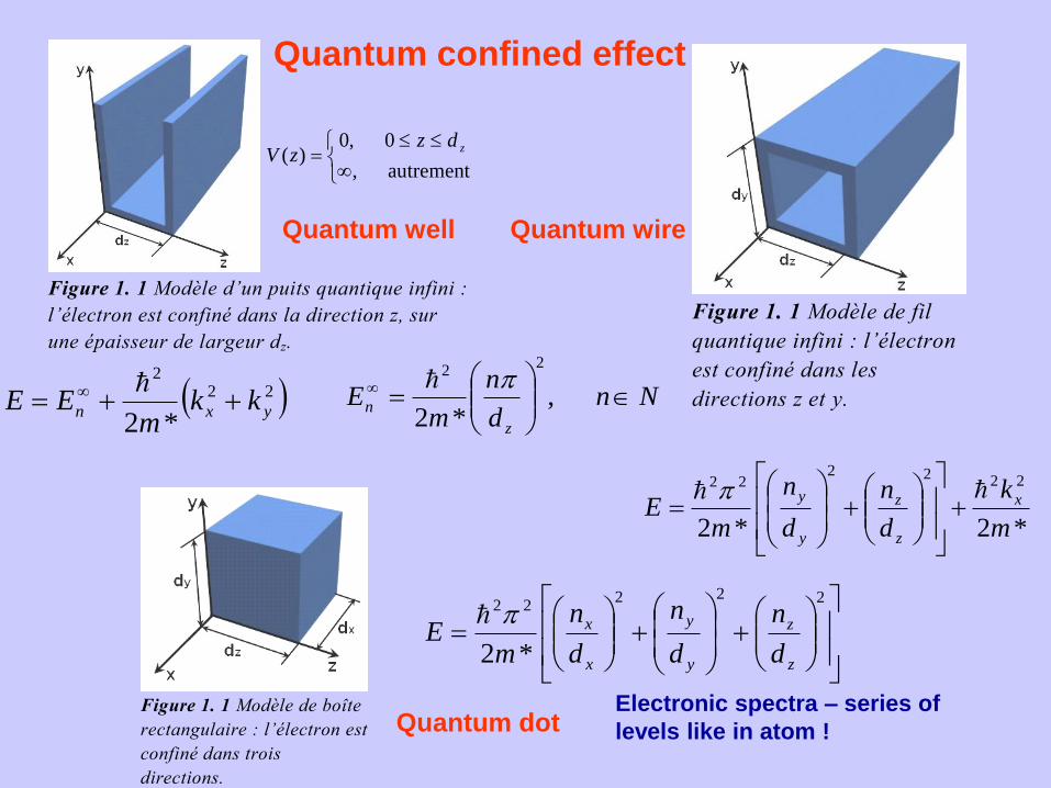
Quantum confined effect
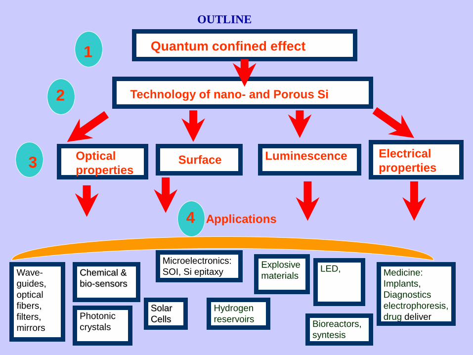
Evolution of modern semiconductor physics:
from bulk to nano
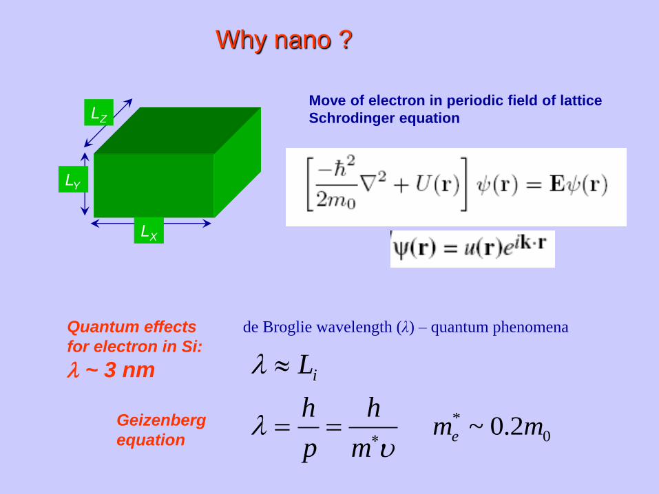
Why nano ?
LX
LY
LZ
de Broglie wavelength (λ) – quantum phenomena Quantum effects
for electron in Si:
~ 3 nm
m
h
p
h
Li
Move of electron in periodic field of lattice
Schrodinger equation
Geizenberg
equation 0
* 2.0~ mme
autrement,
0,0)(
zdzzV
Figure 1. 1 Modèle d’un puits quantique infini :
l’électron est confiné dans la direction z, sur
une épaisseur de largeur dz.
Nn
d
n
mE
z
n
,
*2
22
222
*2yxn kk
mEE
Figure 1. 1 Modèle de fil
quantique infini : l’électron
est confiné dans les
directions z et y.
*2*2
222222
m
k
d
n
d
n
mE x
z
z
y
y
Figure 1. 1 Modèle de boîte
rectangulaire : l’électron est
confiné dans trois
directions.
22222
*2 z
z
y
y
x
x
d
n
d
n
d
n
mE
Quantum confined effect
Quantum well Quantum wire
Quantum dot Electronic spectra – series of
levels like in atom !
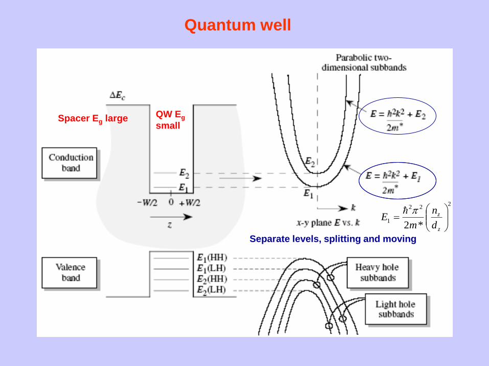
Quantum well
Separate levels, splitting and moving
Spacer Eg large QW Eg
small
222
1*2
z
z
d
n
mE
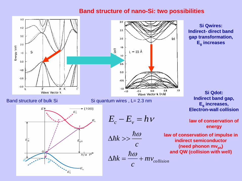
Band structure of nano-Si: two possibilities
Band structure of bulk Si Si quantum wires , L= 2.3 nm
law of conservation of
energy
collisionmvc
k
ck
hEE vc
law of conservation of impulse in
indirect semiconductor
(need phonon mvph)
and QW (collision with well)
Si Qwires:
Indirect- direct band
gap transformation,
Eg increases
Si Qdot:
Indirect band gap,
Eg increases,
Electron-wall collision
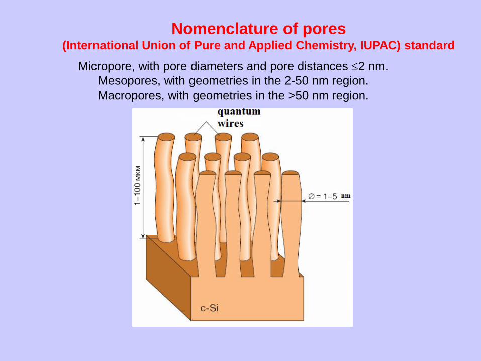
Micropore, with pore diameters and pore distances 2 nm.
Mesopores, with geometries in the 2-50 nm region.
Macropores, with geometries in the >50 nm region.
Nomenclature of pores (International Union of Pure and Applied Chemistry, IUPAC) standard
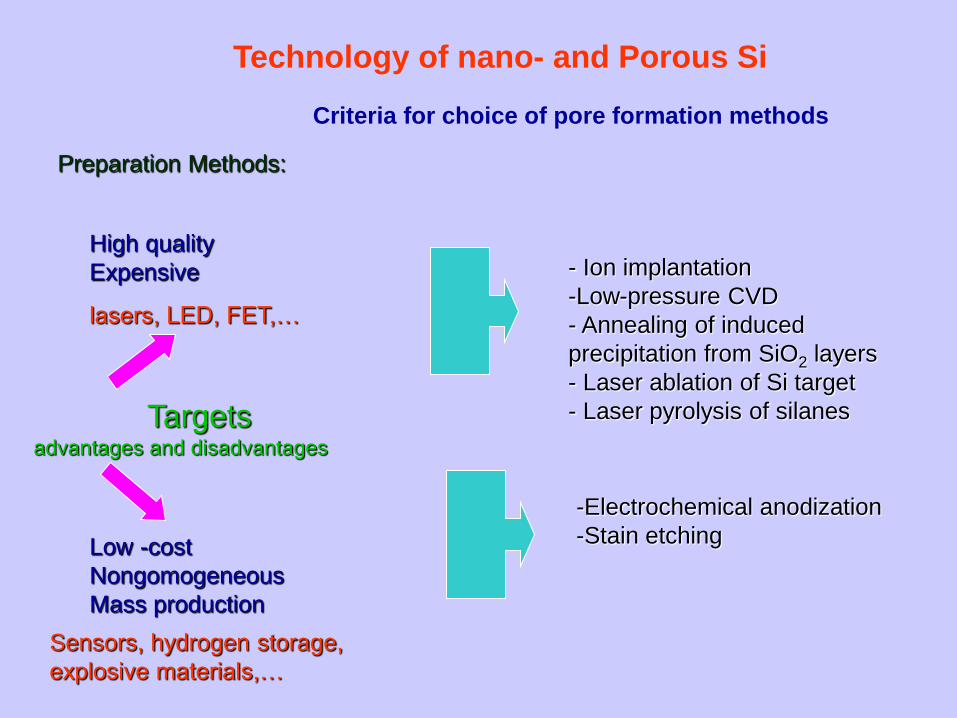
Low -cost
Nongomogeneous
Mass production
High quality
Expensive - Ion implantation
-Low-pressure CVD
- Annealing of induced
precipitation from SiO2 layers
- Laser ablation of Si target
- Laser pyrolysis of silanes
-Electrochemical anodization
-Stain etching
Targets advantages and disadvantages
Criteria for choice of pore formation methods
Preparation Methods:
Sensors, hydrogen storage,
explosive materials,…
lasers, LED, FET,…
Technology of nano- and Porous Si
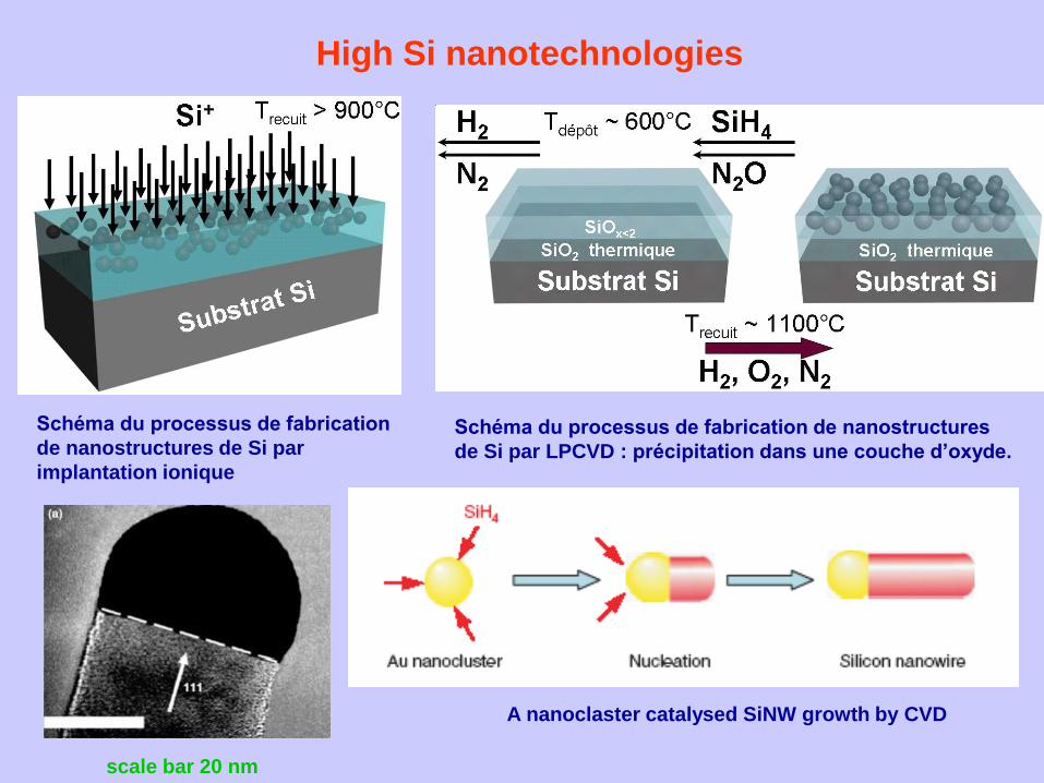
High Si nanotechnologies
Schéma du processus de fabrication
de nanostructures de Si par
implantation ionique
Schéma du processus de fabrication de nanostructures
de Si par LPCVD : précipitation dans une couche d’oxyde.
A nanoclaster catalysed SiNW growth by CVD
scale bar 20 nm
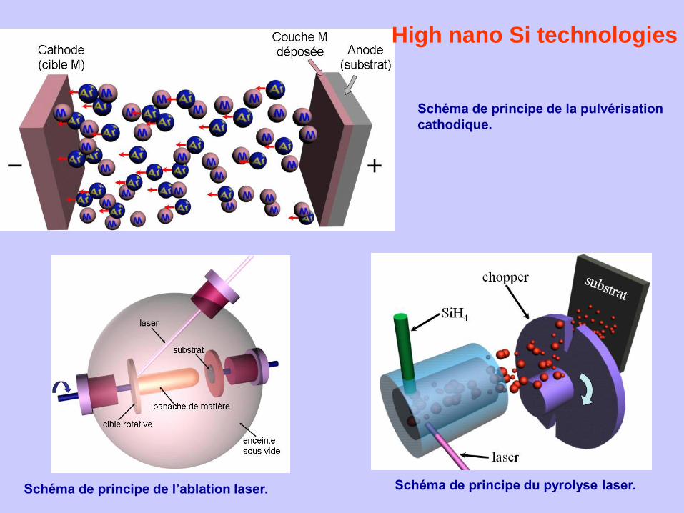
Schéma de principe de la pulvérisation
cathodique.
Schéma de principe de l’ablation laser. Schéma de principe du pyrolyse laser.
High nano Si technologies
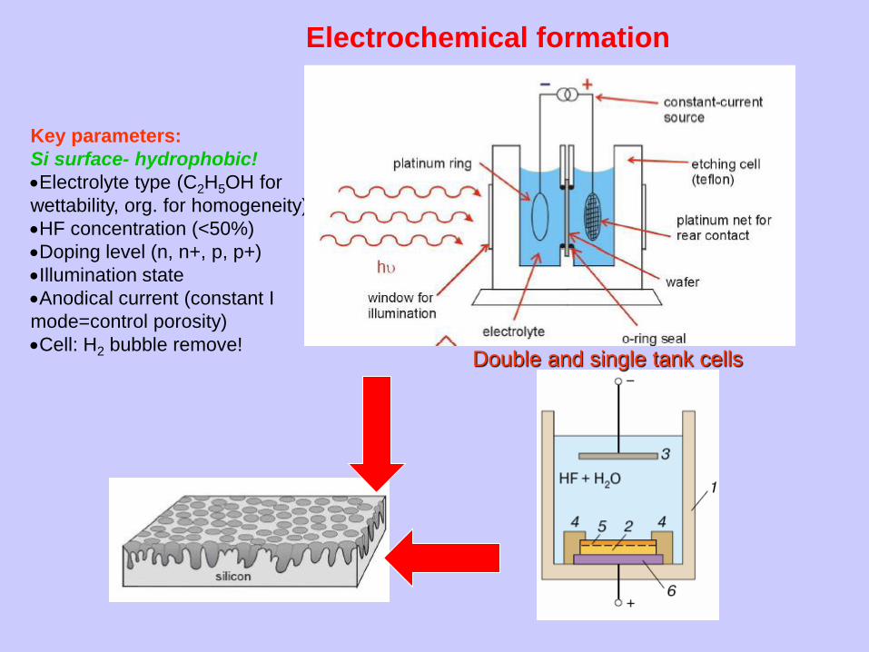
Key parameters:
Si surface- hydrophobic!
Electrolyte type (C2H5OH for
wettability, org. for homogeneity)
HF concentration (<50%)
Doping level (n, n+, p, p+)
Illumination state
Anodical current (constant I
mode=control porosity)
Cell: H2 bubble remove!
Double and single tank cells
Electrochemical formation
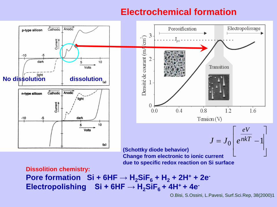
Dissolition chemistry:
Pore formation Si + 6HF → H2SiF6 + H2 + 2H+ + 2e-
Electropolishing Si + 6HF → H2SiF6 + 4H+ + 4e-
Electrochemical formation
(Schottky diode behavior)
Change from electronic to ionic current
due to specific redox reaction on Si surface
No dissolution dissolution
O.Bisi, S.Ossini, L.Pavesi, Surf.Sci.Rep, 38(2000)1
0 1
eV
nkTJ J e
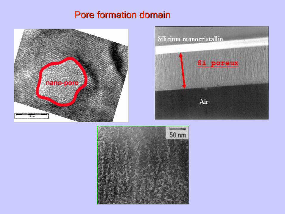
Pore formation domain
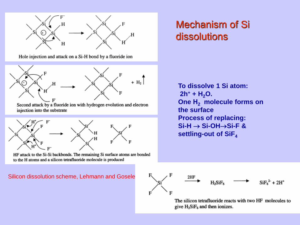
To dissolve 1 Si atom:
2h+ + H2O.
One Н2 molecule forms on
the surface
Process of replacing:
Si-H Si-OHSi-F &
settling-out of SiF4
Mechanism of Si
dissolutions
Silicon dissolution scheme, Lehmann and Gosele
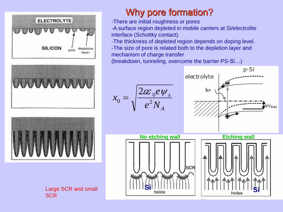
Why pore formation? -There are initial roughness or pores
-A surface region depleted in mobile carriers at Si/electrolite
interface (Schottky contact).
-The thickness of depleted region depends on doping level.
-The size of pore is related both to the depletion layer and
mechanism of charge transfer
(breakdown, tunneling, overcome the barrier PS-Si…)
Large SCR and small
SCR
Si Si
Etching wall No etching wall
A
s
Ne
ex
2
00
2
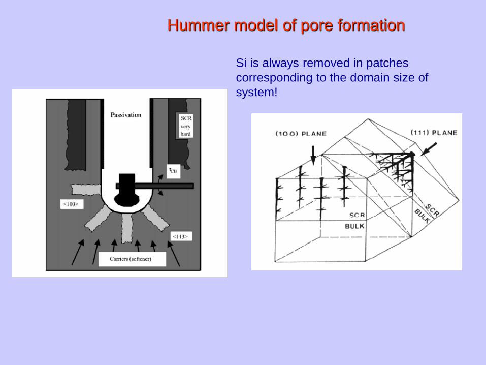
Hummer model of pore formation
Si is always removed in patches
corresponding to the domain size of
system!
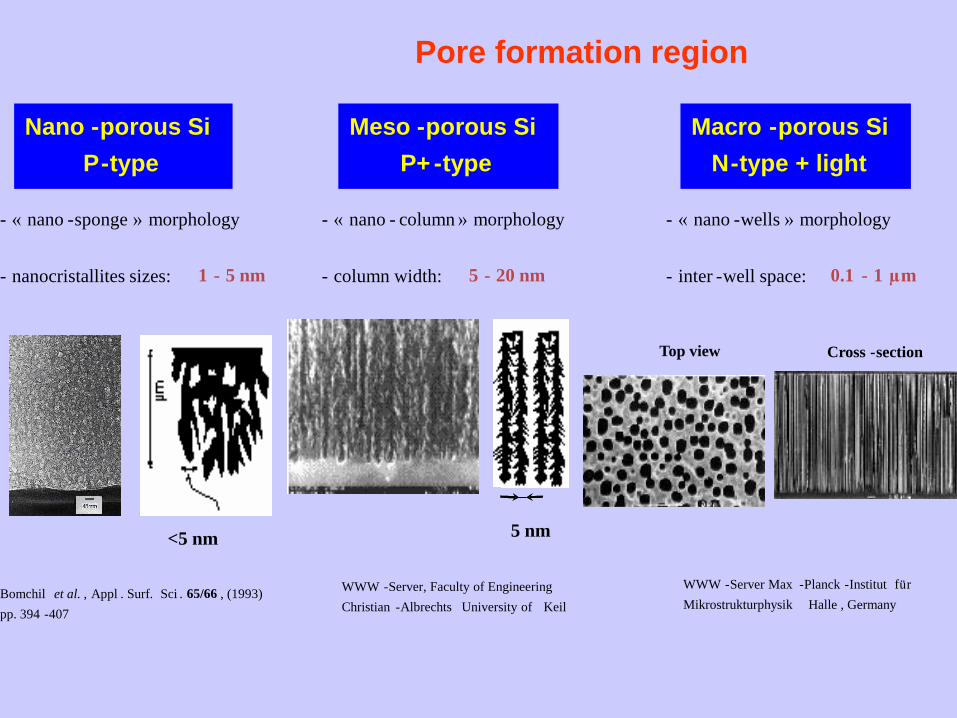
Pore formation region
Top view Cross - section
WWW - Server Max - Planck - Institut f ü r
Mikrostrukturphysik Halle , Germany
WWW - Server, Faculty of Engineering
Christian - Albrechts University of Keil
5 nm <5 nm
Bomchil et al. , Appl . Surf. Sci . 65/66 , (1993)
pp. 394 - 407
- « nano - sponge » morphology
- nanocristallites sizes: 1 - 5 nm
Nano - porous Si
P - type
Meso - porous Si
P+ - type
Macro - porous Si
N - type + light
- « nano - column » morphology
- column width: 5 - 20 nm
- « nano - wells » morphology
- inter - well space: 0.1 - 1 µ m
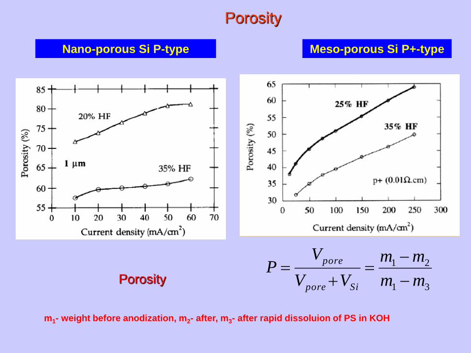
Porosity
Nano-porous Si P-type Meso-porous Si P+-type
31
21
mm
mm
VV
VP
Sipore
pore
Porosity
m1- weight before anodization, m2- after, m3- after rapid dissoluion of PS in KOH
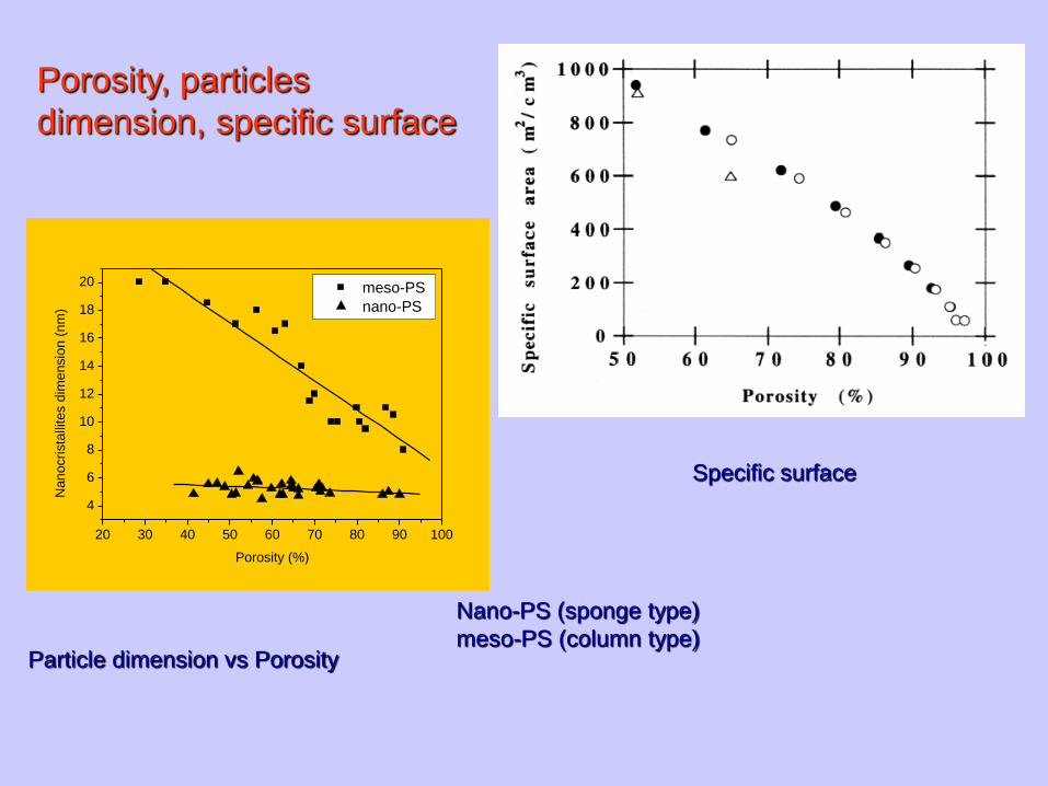
20 30 40 50 60 70 80 90 100
4
6
8
10
12
14
16
18
20
meso-PS
nano-PS
Nanocri
sta
llite
s d
imensio
n (
nm
)
Porosity (%)
Particle dimension vs Porosity
Specific surface
Porosity, particles
dimension, specific surface
Nano-PS (sponge type)
meso-PS (column type)
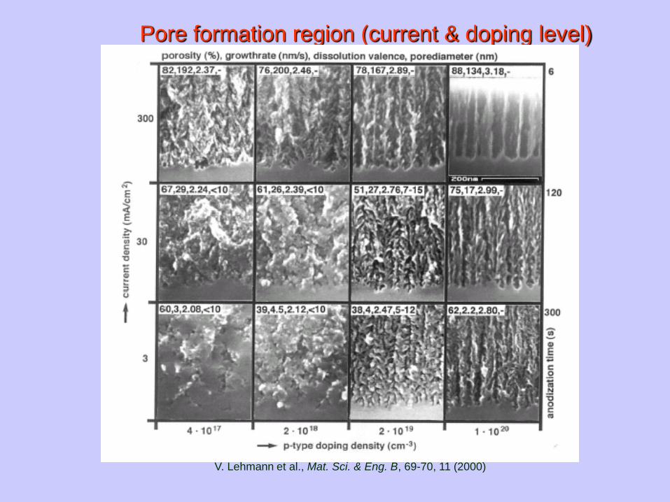
Pore formation region (current & doping level)
V. Lehmann et al., Mat. Sci. & Eng. B, 69-70, 11 (2000)
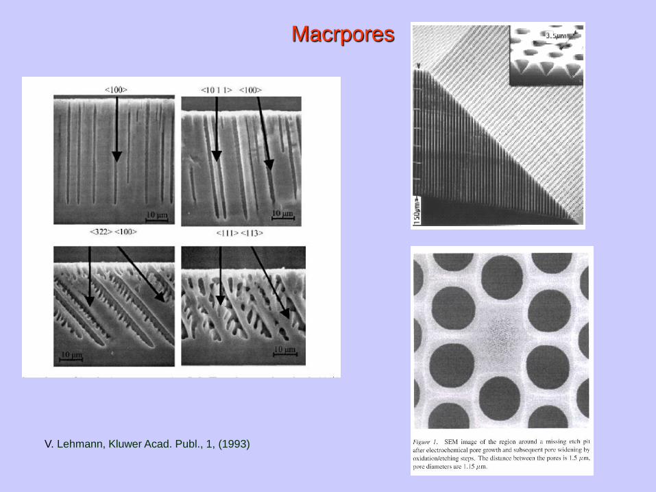
Macrpores
V. Lehmann, Kluwer Acad. Publ., 1, (1993)
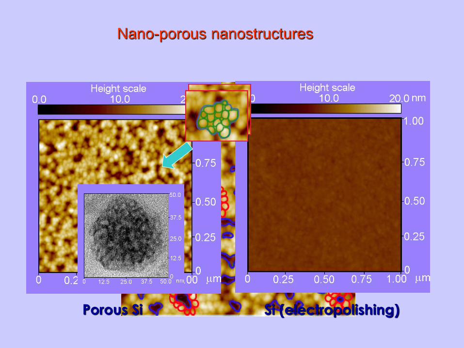
Nano-porous nanostructures
Porous Si Si (electropolishing)
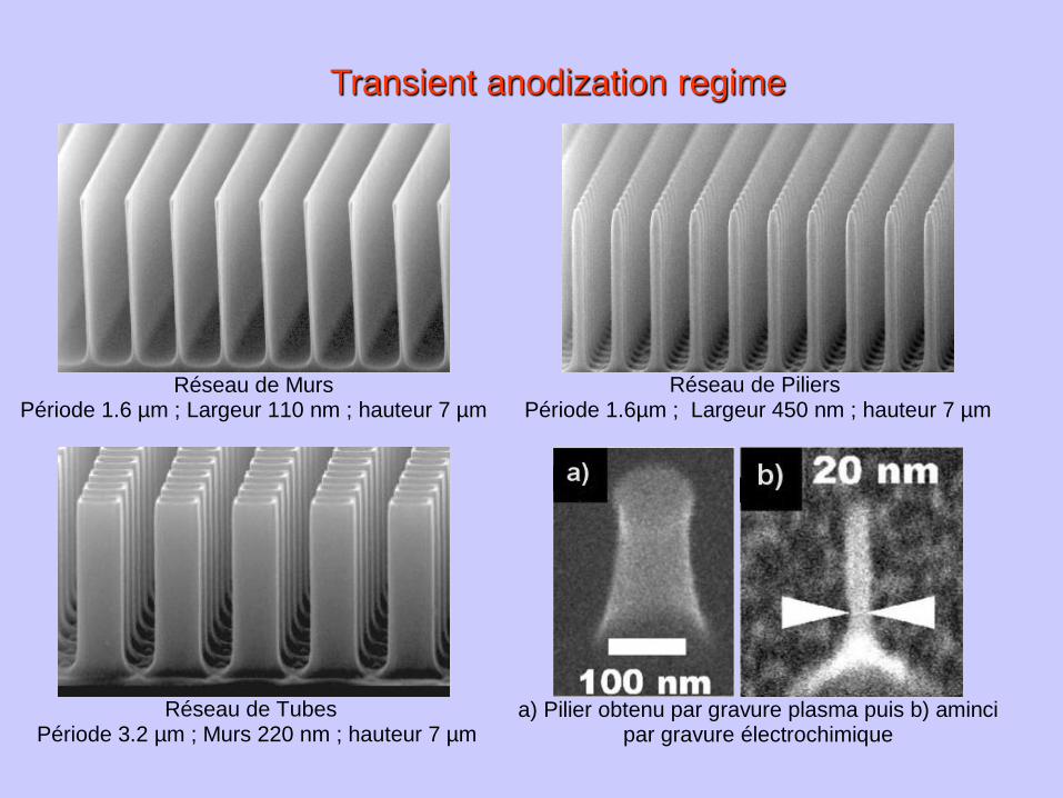
Transient anodization regime
Réseau de Murs
Période 1.6 µm ; Largeur 110 nm ; hauteur 7 µm
Réseau de Piliers
Période 1.6µm ; Largeur 450 nm ; hauteur 7 µm
Réseau de Tubes
Période 3.2 µm ; Murs 220 nm ; hauteur 7 µm
a) Pilier obtenu par gravure plasma puis b) aminci
par gravure électrochimique
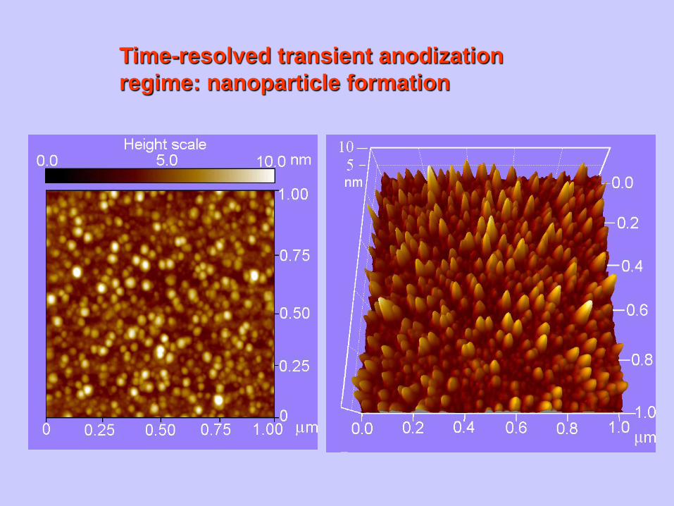
Time-resolved transient anodization
regime: nanoparticle formation
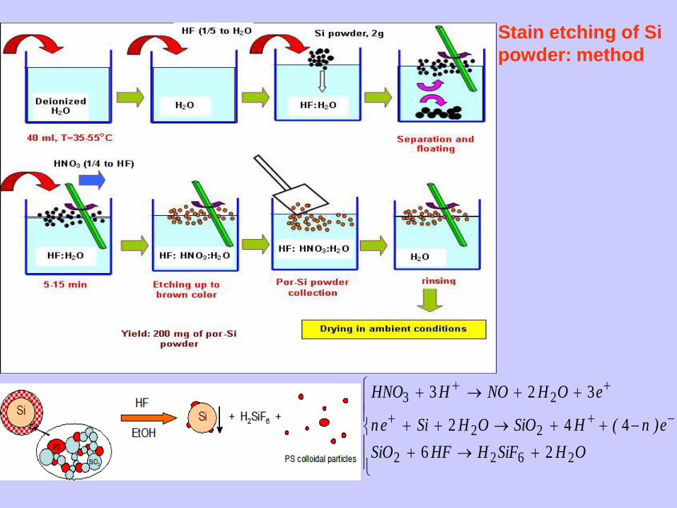
Stain etching of Si
powder: method
OHSiFHHFSiO
e)n(HSiOOHSien
eOHNOHHNO
2622
22
23
26
442
323
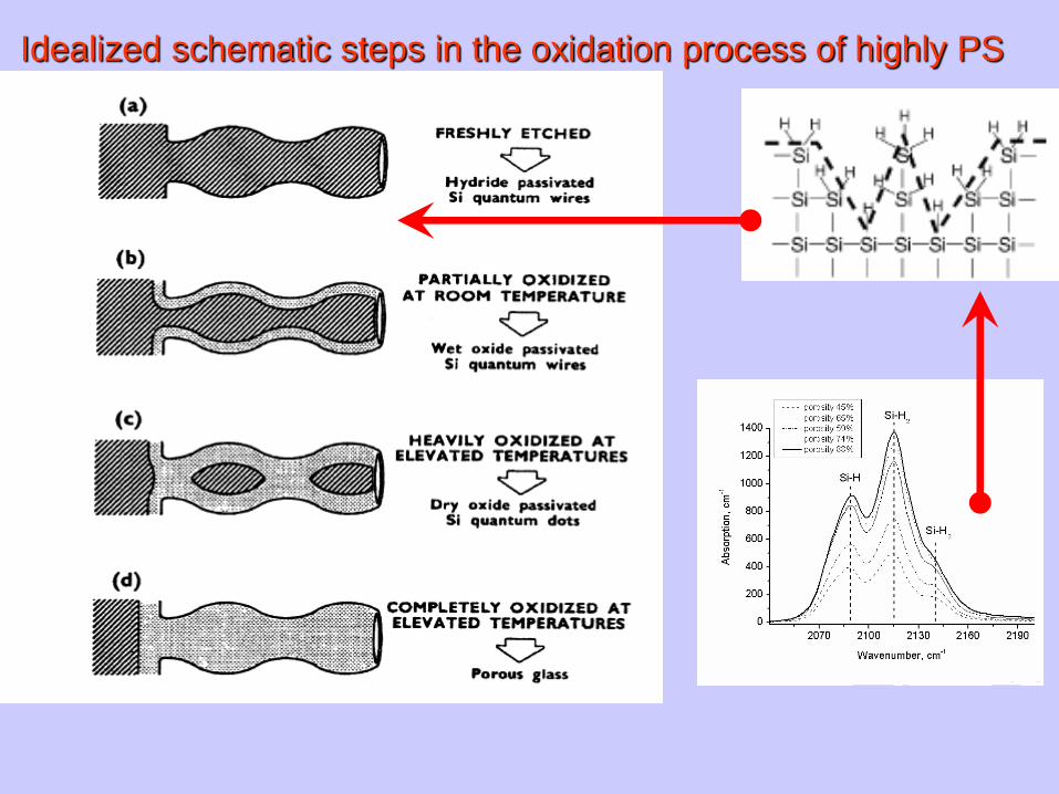
Idealized schematic steps in the oxidation process of highly PS
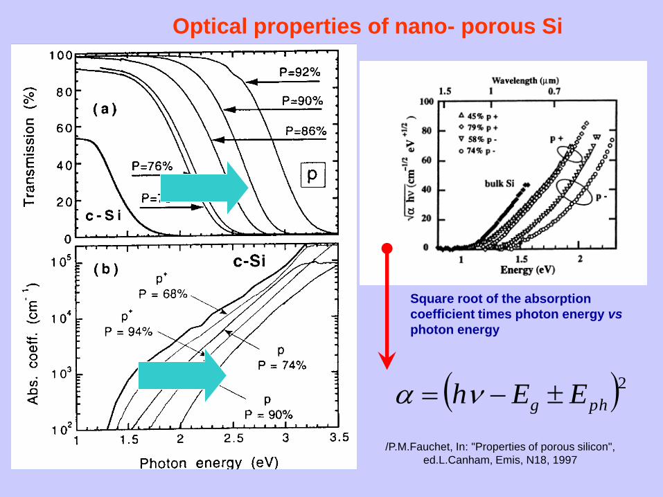
Optical properties of nano- porous Si
/P.M.Fauchet, In: "Properties of porous silicon",
ed.L.Canham, Emis, N18, 1997
Square root of the absorption
coefficient times photon energy vs
photon energy
2phg EEh
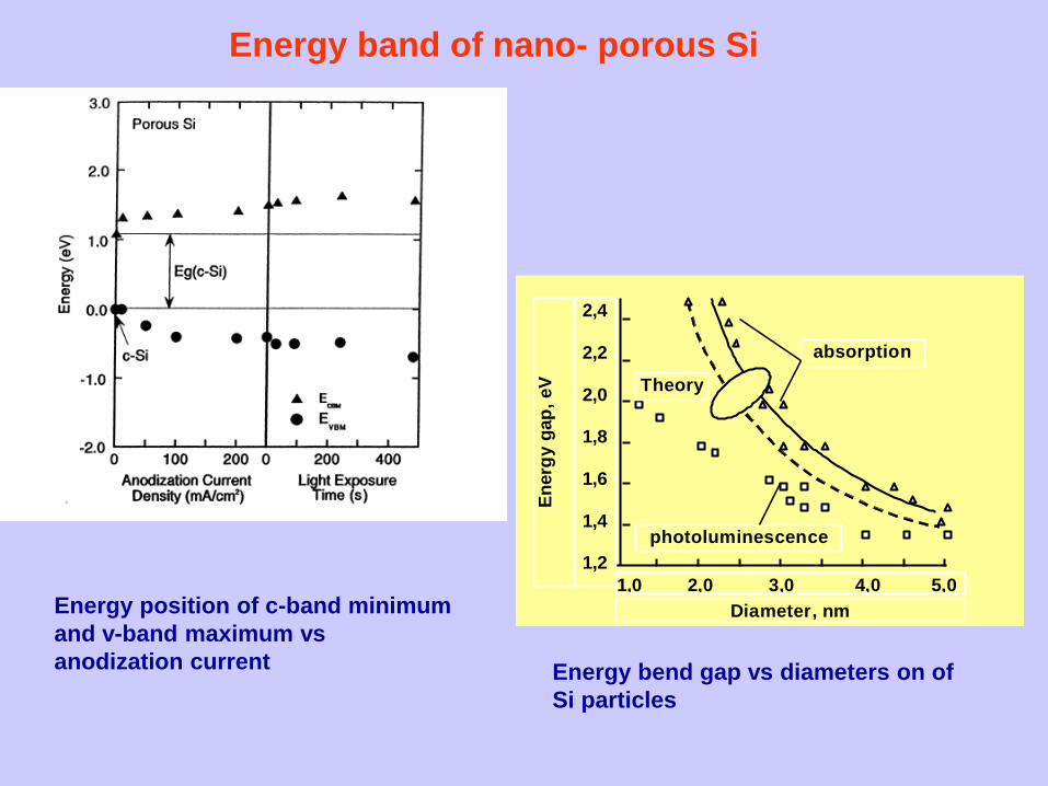
Energy position of c-band minimum
and v-band maximum vs
anodization current
Energy band of nano- porous Si
2,4
2,2
2,0
1,8
1,6
1,4
1,2 E
nerg
y g
ap
, eV
1,0 2,0 3,0 4,0 5,0
Diameter, nm
absorption
Theory
photoluminescence
Energy bend gap vs diameters on of
Si particles
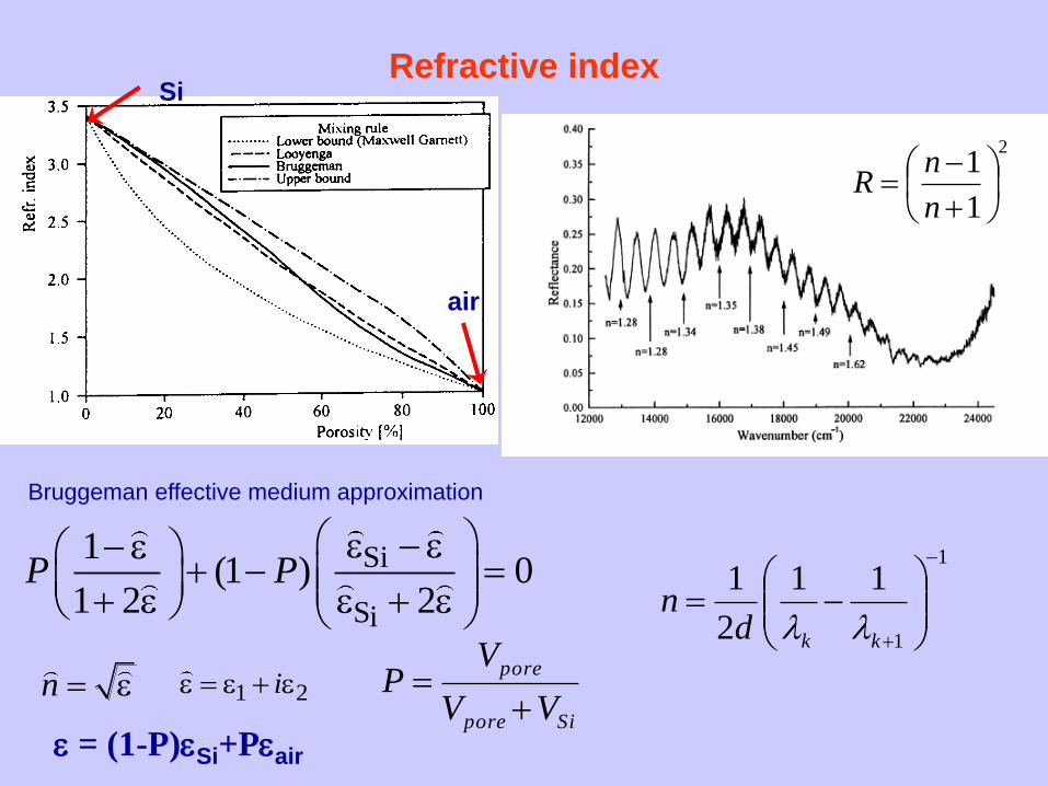
Refractive index
= (1-P)Si+Pair
Si
Si
1(1 ) 0
1 2 2P P
Bruggeman effective medium approximation
Sipore
pore
VV
VP
1
1
11
2
1
kkdn
2
1
1
n
nR
n
Si
air
1 2i
/M.Thonissen, In: "Properties of porous silicon",
ed.L.Canham, Emis, N18, 1997, p.349/
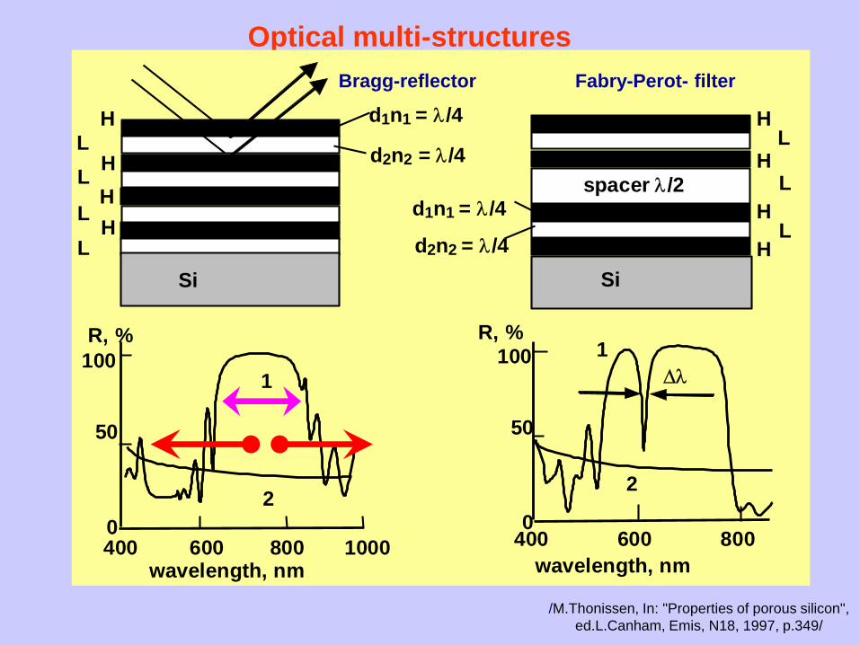
Optical multi-structures
217 нм Si Si
d1n1 = /4
d2n2 = /4
H L
H H H
H
L
L
L
L
L
L H
H
H
spacer/2 d1n1 = /4
d2n2 = /4
R, % R, % 100
50
0
100
50
0
400 600 800 1000 400 600 800 wavelength, nm wavelength, nm
1
2
1
2
Fabry-Perot- filter Bragg-reflector
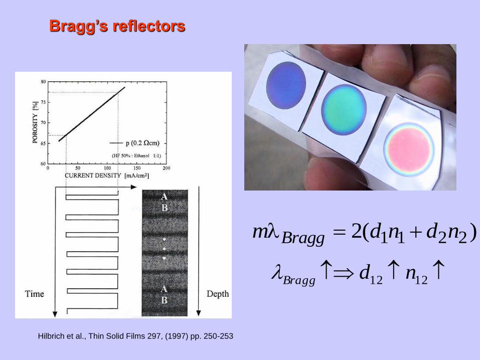
Bragg’s reflectors
Hilbrich et al., Thin Solid Films 297, (1997) pp. 250-253
1212 ndBragg
1 1 2 22( )Braggm d n d n
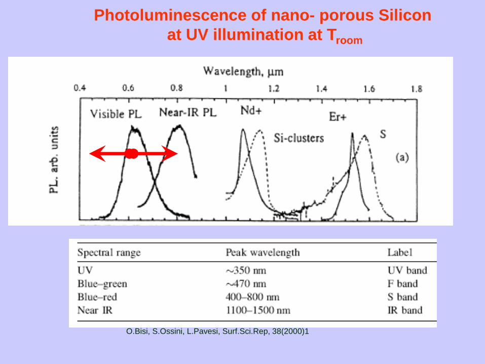
Photoluminescence of nano- porous Silicon
at UV illumination at Troom
O.Bisi, S.Ossini, L.Pavesi, Surf.Sci.Rep, 38(2000)1
Photoluminescence of nano- porous Silicon
2,0 2,5 3,0 3,5 4,0 4,5 5,0 5,5
431
No
rma
lize
d P
L I
nte
ns
ity
(a
.u.)
Energy (eV)
Eex
=4.96eV
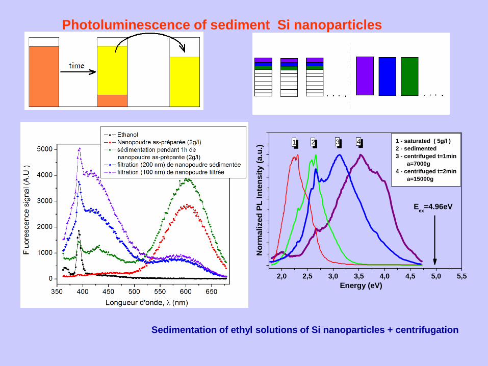
2 1 - saturated ( 5g/l )
2 - sedimented
3 - centrifuged t=1min
a=7000g
4 - centrifuged t=2min
a=15000g
Sedimentation of ethyl solutions of Si nanoparticles + centrifugation
Photoluminescence of sediment Si nanoparticles
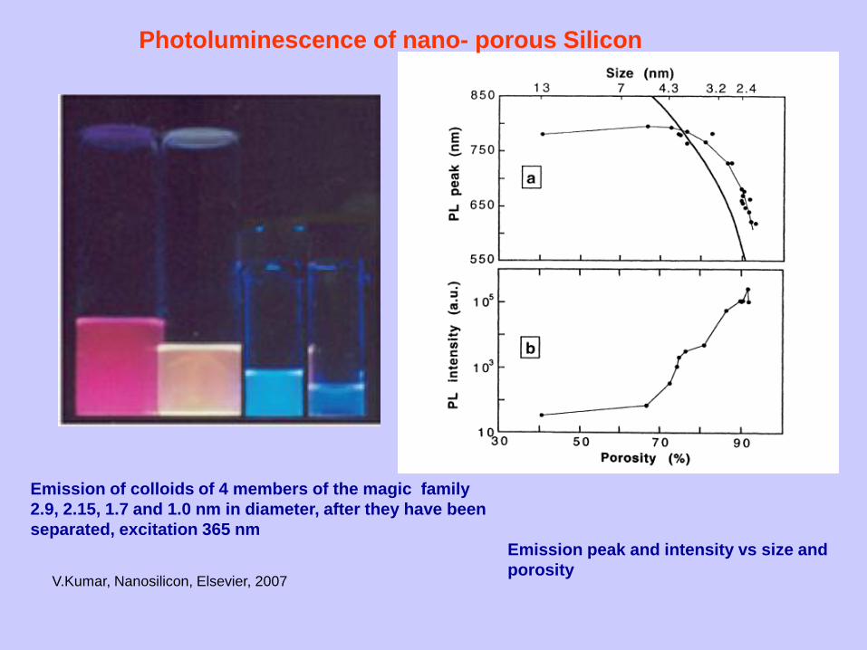
Emission of colloids of 4 members of the magic family
2.9, 2.15, 1.7 and 1.0 nm in diameter, after they have been
separated, excitation 365 nm
Photoluminescence of nano- porous Silicon
Emission peak and intensity vs size and
porosity V.Kumar, Nanosilicon, Elsevier, 2007
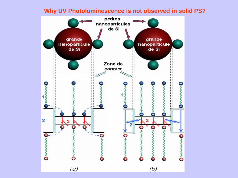
Why UV Photoluminescence is not observed in solid PS?
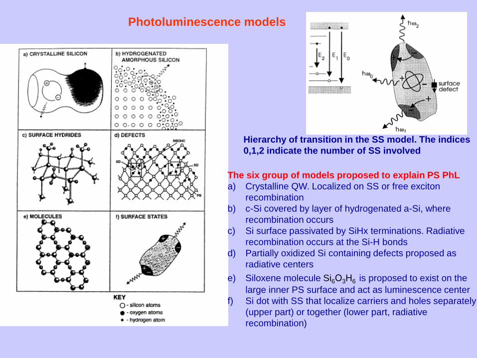
Photoluminescence models
Hierarchy of transition in the SS model. The indices
0,1,2 indicate the number of SS involved
The six group of models proposed to explain PS PhL
a) Crystalline QW. Localized on SS or free exciton
recombination
b) c-Si covered by layer of hydrogenated a-Si, where
recombination occurs
c) Si surface passivated by SiHx terminations. Radiative
recombination occurs at the Si-H bonds
d) Partially oxidized Si containing defects proposed as
radiative centers
e) Siloxene molecule Si6О3Н6 is proposed to exist on the
large inner PS surface and act as luminescence center
f) Si dot with SS that localize carriers and holes separately
(upper part) or together (lower part, radiative
recombination)
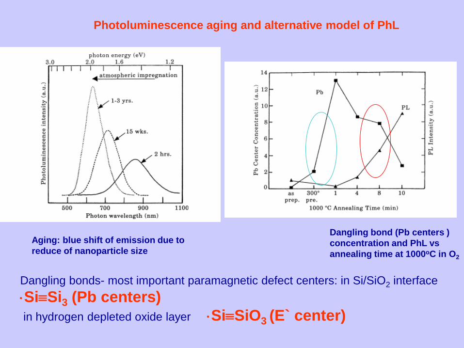
Photoluminescence aging and alternative model of PhL
Aging: blue shift of emission due to
reduce of nanoparticle size
Dangling bonds- most important paramagnetic defect centers: in Si/SiO2 interface
SiSi3 (Pb centers)
in hydrogen depleted oxide layer SiSiO3 (E` center)
Dangling bond (Pb centers )
concentration and PhL vs
annealing time at 1000oC in O2
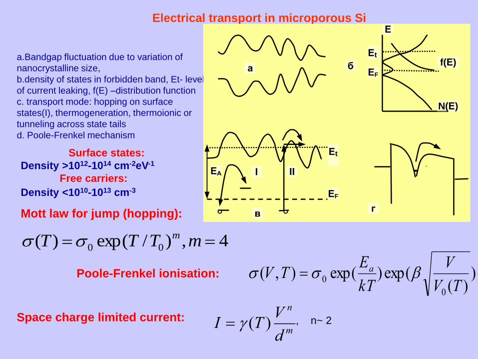
Electrical transport in microporous Si
a.Bandgap fluctuation due to variation of
nanocrystalline size,
b.density of states in forbidden band, Et- level
of current leaking, f(E) –distribution function
c. transport mode: hopping on surface
states(I), thermogeneration, thermoionic or
tunneling across state tails
d. Poole-Frenkel mechanism
))(
exp()exp(),(0
0TV
V
kT
ETV a
m
n
d
VTI )(
4,)/exp()( 00 mTTT m
Poole-Frenkel ionisation:
Space charge limited current: , n~ 2
Mott law for jump (hopping):
Surface states:
Density >1012-1014 cm-2eV-1
Free carriers:
Density <1010-1013 cm-3
Еt
а
вб
бв
г
ЕА І ІІ
ЕF
Еt
ЕF
Е
f(Е)
N(Е)
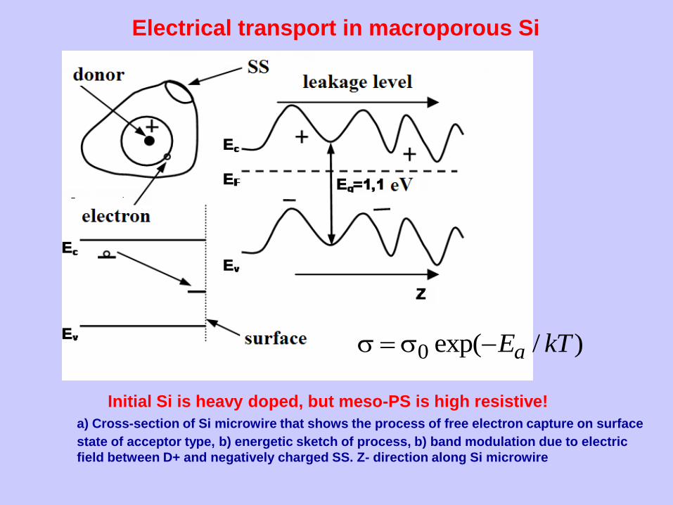
Electrical transport in macroporous Si
a) Cross-section of Si microwire that shows the process of free electron capture on surface
state of acceptor type, b) energetic sketch of process, b) band modulation due to electric
field between D+ and negatively charged SS. Z- direction along Si microwire
0 exp( / )aE kT
Initial Si is heavy doped, but meso-PS is high resistive!
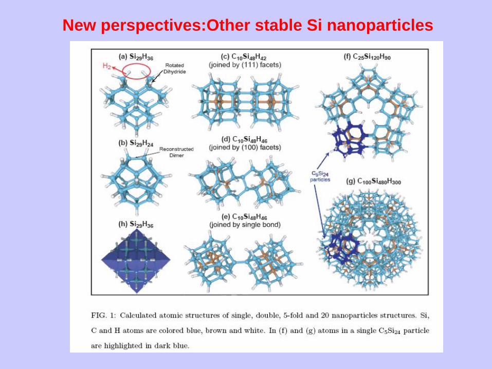
New perspectives:Other stable Si nanoparticles
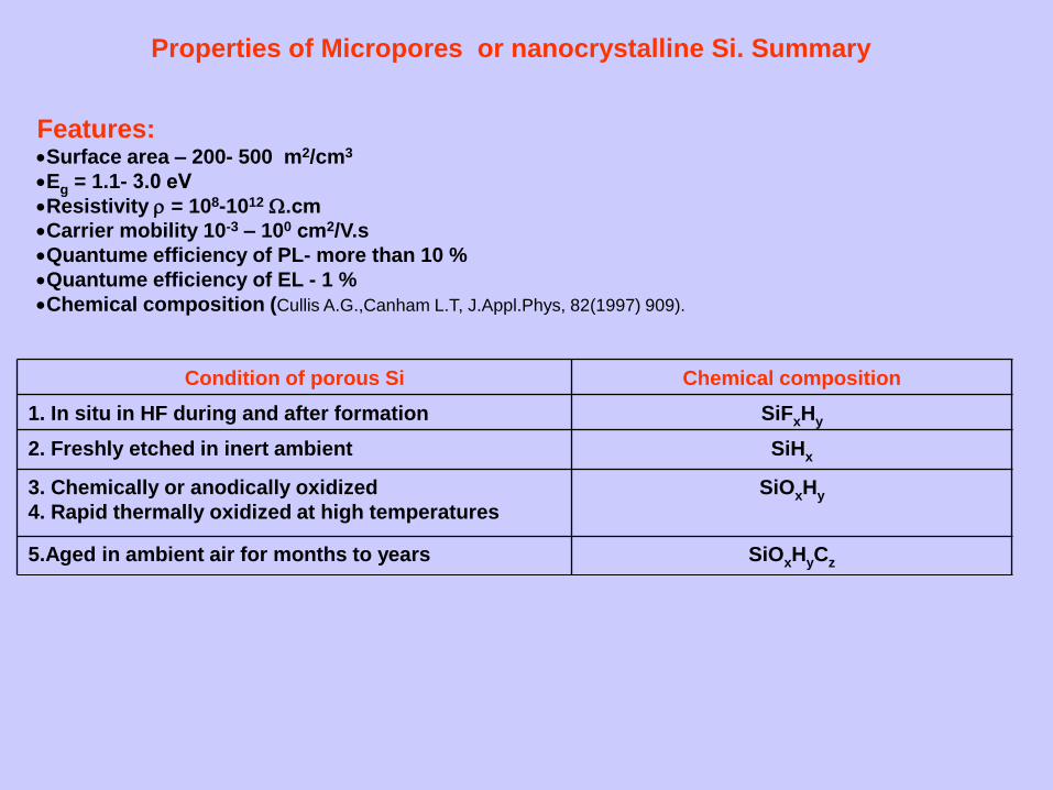
Properties of Micropores or nanocrystalline Si. Summary
Features: Surface area – 200- 500 m2/cm3
Eg = 1.1- 3.0 еV
Resistivity = 108-1012 .сm
Carrier mobility 10-3 – 100 сm2/V.s
Quantume efficiency of PL- more than 10 %
Quantume efficiency of EL - 1 %
Chemical composition (Cullis A.G.,Canham L.T, J.Appl.Phys, 82(1997) 909).
Condition of porous Si Chemical composition
1. In situ in HF during and after formation SiFxHy
2. Freshly etched in inert ambient SiHx
3. Chemically or anodically oxidized
4. Rapid thermally oxidized at high temperatures
SiOxHy
5.Aged in ambient air for months to years SiOxHyCz