630 IEEE TRANSACTIONS ON ANTENNAS AND PROPAGATION, …
9
630 IEEE TRANSACTIONS ON ANTENNAS AND PROPAGATION, VOL. 56, NO. 3, MARCH 2008 A Novel Single-Feed Circular Microstrip Antenna With Reconfigurable Polarization Capability Boyon Kim, Student Member, IEEE, Bo Pan, Student Member, IEEE, Symeon Nikolaou, Young-Sik Kim, Member, IEEE, John Papapolymerou, Senior Member, IEEE, and Manos M. Tentzeris, Senior Member, IEEE Abstract—A single-feed circular microstrip antenna with recon- figurable polarization capability is proposed. This antenna has a simple structure, which consists of a radiating circular patch, five switches (PIN diode), three matching stubs, and a 50 microstrip feed line. It can be switched between 4 different states: two states (low-frequency and high-frequency) for linear polarization (LP), one state for left hand circular polarization (LHCP) and one for right hand circular polarization (RHCP) by controlling the bias voltage of two PIN diodes. At the same time, three switchable matching stubs are used for matching every polarization state. Simulation results and experimental results show that the pro- posed antenna demonstrates a low cross polarization level, good impedance bandwidth, and a very good axial ratio in the circularly polarized states. Index Terms—Circular polarization, linear polarization, mi- crostrip antenna, PIN diode, reconfigurable polarization. I. INTRODUCTION R ECONFIGURABLE microstrip antennas for frequency agility and polarization diversity have advantages of frequency reuse for doubling the system capability and a high degree of polarization control to optimize system performance [1]. Moreover, these reconfigurable antennas have been re- ported to achieve polarization diversity and reconfigurability [2]–[4] that offer an improved effectiveness in receiving the communication signal and have an exceptional ability of reducing multipath fading. In addition, many reconfigurable antennas with polarization diversity between linear and circular polarization [5] and two circular polarizations (i.e., LHCP and RHCP) [1]–[3] have been discussed in past literature. Due to the significant difference in the input impedance, the matching covered only one polarization state between LP and CP [5] or LHCP and RHCP [6], [7]. In [6], the impedance seems to be matched well in both LP and CP, but resonant frequencies in CP have matched in only one operation status. Although impedance matching was considered for polarizations in [8], it was not clear how input matching could be achieved by optimizing both polarization senses. Therefore, impedance matching techniques are necessary for all polarization senses. A reconfigurable Manuscript received July 12, 2006; revised March 11, 2007. B. Kim is with the Semiconductor Business, Samsung Electronics, Yongin 446-711, Korea (e-mail: [email protected]). B. Pan, S. Nikolaou, J. Papapolymerou, and M. M. Tentzeris are with the School of Electrical and Computer Engineering, Georgia Institute of Technology, Atlanta, GA 30332 USA. Y.-S. Kim is with the Department of Radio Sciences and Engineering, Korea University, Seoul 136-701, Korea. Digital Object Identifier 10.1109/TAP.2008.916894 matching network for the radiation pattern diversity using short and open stubs has been described in [9] for an annular slot antenna operating at 5.8 GHz. Based on the similar concept in reconfigurable matching network, the impedance matching can be obtained at both two different frequencies in LP and same frequency in LHCP or RHCP. PIN diodes which are used for switching the polarization are commonly used switching devices for RF and microwave front-end application systems, because they have attractive properties such as low insertion loss, good isolation, low power handling, and low cost [10]. In this paper, the authors present for the first time, the design, fabrication, and measurement of a novel single-feed circular mi- crostrip antenna with reconfigurable polarization capability for all polarization states. The proposed antenna utilizes an etched “ ” shaped slot line on the top of the circular microstrip patch. To switch the polarization states, two PIN diodes are installed on the inset of the “ ” shaped slot line. Full-wave simulations were carried out using IE3D with good matching performance for all polarization states [11]. Further- more, the simulations were validated by comparing the simu- lated and measured results which show a good agreement be- tween them. Concerning the contents of this paper, Section II discusses the design process of the proposed antenna, including its ge- ometry and operation principle for reconfigurable polarization capabilities (Section II-A), the switchable matching for all po- larizations (Section II-B) and the application of PIN-diodes for the matching implementation (Section II-C). Section III focuses on the antenna performance for the both LP and CP modes. The effect of the most critical geometrical parameters on the CP per- formance is studied in Section IV, and finally conclusion is ad- dressed in Section V. II. ANTENNA DESIGN WITH RECONFIGURABLE POLARIZATION CAPABILITIES The geometry of the proposed single-feed circular mi- crostrip antenna is shown in Fig. 1. The circular patch of radius is etched on a sheet of RT/duroid 5880 printed circuit board (thickness, mil and relative dielectric constant, ). For the arc slot, the inner side radius of the arc slot is , and the central angle is . The ground plane dimensions are 100 100 mm . The length and width of the insets are determined by the size of the PIN diode . The feed line is composed of a 50 microstrip and three matching stubs ( , and ) which are connected to the feed line by PIN diodes (#1, #2, and #3) to allow for the matching of the four different polarization states. To control the polarization 0018-926X/$25.00 © 2008 IEEE Authorized licensed use limited to: Georgia Institute of Technology. Downloaded on December 15, 2008 at 17:14 from IEEE Xplore. Restrictions apply.
Transcript of 630 IEEE TRANSACTIONS ON ANTENNAS AND PROPAGATION, …

630 IEEE TRANSACTIONS ON ANTENNAS AND PROPAGATION, VOL. 56, NO. 3, MARCH 2008
A Novel Single-Feed Circular Microstrip AntennaWith Reconfigurable Polarization Capability
Boyon Kim, Student Member, IEEE, Bo Pan, Student Member, IEEE, Symeon Nikolaou,Young-Sik Kim, Member, IEEE, John Papapolymerou, Senior Member, IEEE, and
Manos M. Tentzeris, Senior Member, IEEE
Abstract—A single-feed circular microstrip antenna with recon-figurable polarization capability is proposed. This antenna has asimple structure, which consists of a radiating circular patch, fiveswitches (PIN diode), three matching stubs, and a 50microstripfeed line. It can be switched between 4 different states: two states(low-frequency and high-frequency) for linear polarization (LP),one state for left hand circular polarization (LHCP) and one forright hand circular polarization (RHCP) by controlling the biasvoltage of two PIN diodes. At the same time, three switchablematching stubs are used for matching every polarization state.Simulation results and experimental results show that the pro-posed antenna demonstrates a low cross polarization level, goodimpedance bandwidth, and a very good axial ratio in the circularlypolarized states.
Index Terms—Circular polarization, linear polarization, mi-crostrip antenna, PIN diode, reconfigurable polarization.
I. INTRODUCTION
RECONFIGURABLE microstrip antennas for frequencyagility and polarization diversity have advantages of
frequency reuse for doubling the system capability and a highdegree of polarization control to optimize system performance[1]. Moreover, these reconfigurable antennas have been re-ported to achieve polarization diversity and reconfigurability[2]–[4] that offer an improved effectiveness in receiving thecommunication signal and have an exceptional ability ofreducing multipath fading. In addition, many reconfigurableantennas with polarization diversity between linear and circularpolarization [5] and two circular polarizations (i.e., LHCP andRHCP) [1]–[3] have been discussed in past literature. Due tothe significant difference in the input impedance, the matchingcovered only one polarization state between LP and CP [5] orLHCP and RHCP [6], [7]. In [6], the impedance seems to bematched well in both LP and CP, but resonant frequencies in CPhave matched in only one operation status. Although impedancematching was considered for polarizations in [8], it was notclear how input matching could be achieved by optimizing bothpolarization senses. Therefore, impedance matching techniquesare necessary for all polarization senses. A reconfigurable
Manuscript received July 12, 2006; revised March 11, 2007.B. Kim is with the Semiconductor Business, Samsung Electronics, Yongin
446-711, Korea (e-mail: [email protected]).B. Pan, S. Nikolaou, J. Papapolymerou, and M. M. Tentzeris are with
the School of Electrical and Computer Engineering, Georgia Institute ofTechnology, Atlanta, GA 30332 USA.
Y.-S. Kim is with the Department of Radio Sciences and Engineering, KoreaUniversity, Seoul 136-701, Korea.
Digital Object Identifier 10.1109/TAP.2008.916894
matching network for the radiation pattern diversity using shortand open stubs has been described in [9] for an annular slotantenna operating at 5.8 GHz. Based on the similar conceptin reconfigurable matching network, the impedance matchingcan be obtained at both two different frequencies in LP andsame frequency in LHCP or RHCP. PIN diodes which are usedfor switching the polarization are commonly used switchingdevices for RF and microwave front-end application systems,because they have attractive properties such as low insertionloss, good isolation, low power handling, and low cost [10].
In this paper, the authors present for the first time, the design,fabrication, and measurement of a novel single-feed circular mi-crostrip antenna with reconfigurable polarization capability forall polarization states. The proposed antenna utilizes an etched“ ” shaped slot line on the top of the circular microstrip patch.To switch the polarization states, two PIN diodes are installedon the inset of the “ ” shaped slot line.
Full-wave simulations were carried out using IE3D with goodmatching performance for all polarization states [11]. Further-more, the simulations were validated by comparing the simu-lated and measured results which show a good agreement be-tween them.
Concerning the contents of this paper, Section II discussesthe design process of the proposed antenna, including its ge-ometry and operation principle for reconfigurable polarizationcapabilities (Section II-A), the switchable matching for all po-larizations (Section II-B) and the application of PIN-diodes forthe matching implementation (Section II-C). Section III focuseson the antenna performance for the both LP and CP modes. Theeffect of the most critical geometrical parameters on the CP per-formance is studied in Section IV, and finally conclusion is ad-dressed in Section V.
II. ANTENNA DESIGN WITH RECONFIGURABLE
POLARIZATION CAPABILITIES
The geometry of the proposed single-feed circular mi-crostrip antenna is shown in Fig. 1. The circular patch ofradius is etched on a sheet of RT/duroid 5880 printed circuitboard (thickness, mil and relative dielectric constant,
). For the arc slot, the inner side radius of the arc slotis , and the central angle is . The ground plane dimensionsare 100 100 mm . The length and width of the insets aredetermined by the size of the PIN diode . The feedline is composed of a 50 microstrip and three matching stubs( , and ) which are connected to the feed line byPIN diodes (#1, #2, and #3) to allow for the matching of thefour different polarization states. To control the polarization
0018-926X/$25.00 © 2008 IEEE
Authorized licensed use limited to: Georgia Institute of Technology. Downloaded on December 15, 2008 at 17:14 from IEEE Xplore. Restrictions apply.
KIM et al.: A NOVEL SINGLE-FEED CIRCULAR MICROSTRIP ANTENNA 631
Fig. 1. Geometry of a novel single-feed circular microstrip antenna with re-configurable polarization capabilities including the parametric study (� and �).
Fig. 2. The operation mechanism of the proposed antenna.
state of the designed antenna, two PIN diodes are insertedclose to the edge of the slots with diode #4 oriented in thecounter-clockwise direction and the diode #5 oriented in theclockwise direction. The proposed antenna has two main po-larized states; linear polarization (LP) and circular polarization(CP). The characteristics of this antenna are divided into fourcases depending on the bias of the PIN diodes (high-frequencyLP, low-frequency LP, RHCP, and LHCP), as shown in Fig. 2.
A. Reconfigurable Polarization
To radiate linearly polarized waves, both PIN diodes on thecircular patch (#4 and #5) should be biased in either the “on-state” (Ant.1) or the “off-state” (Ant. 2) simultaneously, in orderto guarantee the physically and electrically symmetric shape ofthe circular microstrip patch required to excite the mode.When both PIN diodes are in the “on-state,” they act as electri-cally short circuits. Therefore, the conventional circular patchshape is slightly modified with an arc-shaped slot, leading only
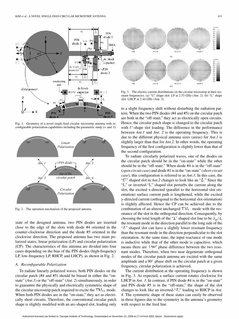
Fig. 3. The electric current distributions on the circular microstrip at their res-onant frequencies. (a) “U” shape slot: LP at 2.53 GHz (Ant. 2). (b) “L” shapeslot: LHCP at 2.44 GHz (Ant. 3).
to a slight frequency shift without disturbing the radiation pat-tern. When the two PIN diodes (#4 and #5) on the circular patchare both in the “off-state,” they act as electrically open circuits.Hence, the circular patch shape is changed to the circular patchwith -shape slot loading. The difference in the performancebetween Ant.1 and Ant. 2 is the operating frequency. This isdue to the different physical antenna sizes (areas) for Ant.1 isslightly larger than that for Ant.2. In other words, the operatingfrequency of the first configuration is slightly lower than that ofthe second configuration.
To radiate circularly polarized waves, one of the diodes onthe circular patch should be in the “on-state” while the othershould be in the “off-state.” When diode #4 is in the “off-state”(open circuit case) and diode #1 is in the “on-state” (short circuitcase), this configuration is referred to as Ant.3. In this case, the“ ” shaped slot in Ant.2 changes to look like an “ .” Since the“L” or inverted-“L” shaped slot perturbs the current along theslot, the excited x-directed (parallel to the horizontal slot ori-entation) surface current path is lengthened, while the excitedy-directed current (orthogonal to the horizontal slot orientation)is slightly affected. Hence the CP can be achieved due to thecombination of an almost unchanged mode with the res-onance of the slot in the orthogonal direction. Consequently, bychoosing the total length of the “ ’ shaped slot line to be ,the resonant mode in the direction parallel to the long side of the“ ” shaped slot can have a slightly lower resonant frequencythan the resonant mode in the direction perpendicular to the slotorientation. At the same time, the input reactance of one modeis inductive while that of the other mode is capacitive, whichmeans there are phase difference between the two reso-nant modes. Therefore, when two near degenerate orthogonalmodes of the circular patch antenna are excited with the sameamplitude and a 90 phase shift on the circular patch at a givenfrequency, circular polarization is achieved.
The current distribution at the operating frequency is shownin Fig. 3. As expected, a surface current rotates clockwise forLHCP in Ant. 3. In contrast, if PIN diode #4 is in the “on-state”and PIN diode #5 is in the “off-state,” the shape of the slotchanges to look like an inverted-“ ,” leading to RHCP in Ant.4. The symmetric shape of these states can easily be observedin these figures due to the symmetry in the antenna’s geometrywith respect to the feed line.
Authorized licensed use limited to: Georgia Institute of Technology. Downloaded on December 15, 2008 at 17:14 from IEEE Xplore. Restrictions apply.

632 IEEE TRANSACTIONS ON ANTENNAS AND PROPAGATION, VOL. 56, NO. 3, MARCH 2008
B. Matching Approach
In [5], it has been observed that the input impedance matchingis presented only for circular polarization, because the patterndegrades when the antenna is linearly polarized. In this paper,we use the reconfigurable stub matching approach with threesingle-stub shunt tuning circuits to address the input impedancematching of linear and circular polarization. When linearly po-larized waves (Ant. 1) are radiated, PIN diode #1 is in the “on-state” in order to connect between the open-circuit stub (i.e.,
) to the 50 ohm feed-line, while PIN diodes #2 and#3 are in the “off-state.” Similarly, to radiate linearly polarizedwaves (Ant. 2) only PIN diode #2 is in the “on-state” to connectbetween the open-circuited stub to the 50 ohmfeed-line, while PIN diodes #1 and #3 are in the “off-state” withrespect to the feed line. To get a good impedance matching forthe two circularly polarized states (Ant. 3 and 4), the short-cir-cuit stub is connected between the edge of thestub and the ground by using a via hole. There are two mainreasons to use the short stub instead of an open stub. Byusing an open stub, the position of the stub will overlap withthe neighboring open stubs ( or ). The other reason isbased on the length of the open stub which is longer than thatof the short stub by , which could be large enough (elec-trically) to radiate. Hence, the stub would no longer be purelyreactive [12]. In addition, the elongated stub would increase theoverall dimensions of the antenna. Since the input impedance isthe same due to the symmetrical geometries with respect to thefeed line, it is possible to use the same short stub for both LHCPand RHCP.
C. Application of PIN Diodes
To achieve the reconfigurable polarization capability,switching components must be used. PIN diodes are the mostcommonly used switching devices for RF and microwavefront-end application systems. The RF equivalent circuit ofthe PIN diode for the ON (forward bias case) and OFF (reversebias case) states is shown in Fig. 4. The PIN diodes whichinclude self-protect resistors of forward-biased current, RFchoke inductors, and dc block capacitors should be isolatedfrom the RF signal. To control the PIN diodes, six dc bias linesare designed with the same size . The bias circuitmust consist of a PIN diode, dc block capacitor, RF choke,and input voltage as shown in Fig. 5. Two dc bias lines areindirectly connected to top part of the circular patch with PINdiodes using “U” shaped slot loading. Three dc bias lines areconnected to each matching stub, which supply dc current toPIN diode 1, 2, 3, 4, and 5; the sixth one is used for dc-isolation,which is connected to the 50 feed line. The equivalent RLCcircuit models (MA4P274CK-287) that include the parasiticpackaging effects can be extracted from the PIN diode datasheet [13]. At the diode on-state, the equivalent circuit is rep-resented by a resistor, , while the diode off-state, theequivalent circuit is represented by a capacitor, pF.Three dc block capacitors of pF are chosen to isolatethe RF components from the dc ones. Since the calculatedvalue of represents a “near shortcircuit” condition, the RF signal will pass through the capacitorwith little loss or reflection. The RF choke inductor isolate the
Fig. 4. Equivalent circuit of a packaged PIN diode in its two bias conditions.(a) on-state (forward bias). (b) Off-state (reverse bias). L = 1:4 nH and Rprepresents the net dissipative resistance in the reverse biased diode and is lesssignificant.
Fig. 5. The configuration in PIN diode biasing circuit.
RF signal from flowing into the dc signal, therefore, very thin( um) quarter-wavelength dc bias lines were used,instead of the RF choke inductors. PIN diodes are used forswitching with a forward voltage of and forwardbias current of mA, respectively. The photograph ofthe proposed antenna is shown in Fig. 6.
III. ANTENNA PERFORMANCE
The return loss, axial ratio, gain, and radiation patterns of theproposed antenna have been simulated and measured for all thedifferent states of the two PIN diodes (#4 and #5) that control thepolarization state as well as for the states of the three PIN diodes(#1, #2 and #3) which connect and disconnect the matchingstubs to the feed line. The geometry of the proposed antenna ismodified according to the on- and off-states of the PIN diodesand features the resulting capability of polarization diversity.Without loss of generality and for simplicity reasons, an infiniteground plane was used in the simulations, assuming a perfectopen-circuit (gap) for the PIN diodes in the off-state. When thediodes are in the on-state, they were modeled as through linesby using metal tape (1.94 1.60 mm ).
Authorized licensed use limited to: Georgia Institute of Technology. Downloaded on December 15, 2008 at 17:14 from IEEE Xplore. Restrictions apply.

KIM et al.: A NOVEL SINGLE-FEED CIRCULAR MICROSTRIP ANTENNA 633
Fig. 6. Photograph of the single-feed circular microstrip antenna for reconfig-urable polarization capability.
The simulations of the proposed antenna were carried outusing IE3D, a commercial electromagnetic simulator based onthe integral equation method and the method of moments. It isobserved that good impedance matching can be achieved for allpolarization (LP and CP) states, as shown in Fig. 7. The differ-ence in the results between the simulated and measured data isdue to the use of an infinite ground in the simulation.
Details of the design parameters and the obtained results forthe four different antenna prototypes are summarized in Table I.The bandwidth for the CP (2.60 % for Ant. 3) is much larger thanthat of the LP (1.17 % for Ant. 1) because two resonant modesradiate simultaneously for the circular polarized case, and onlyone resonant mode radiates for the linear polarized casewhich is similar to the mode of the conventional circular mi-crostrip patch. The simulated and measured axial ratios of theproposed antenna for CP (Ant. 3 and Ant. 4) are shown in Fig. 8where very good agreement is observed. The minimal differenceof the minimum AR point between Ant. 3 and Ant. 4 (less than 5MHz) in simulation can be attributed to the non-symmetry of thematching stubs. Fig. 9 shows the simulated gain of the proposedantenna for LP and CP states, which is near 6 dBi across the op-erational bandwidth. Fig. 10 shows the simulated and measuredradiation patterns at 2.477 GHz and 2.552 GHz for the LP states(Ant. 1 and Ant. 2). The peak gains are observed to be 5.85 dBiand 5.94 dBi for Ant. 1 and Ant. 2, respectively. The cross polar-ization level is below dB at each given frequency in bothAnt. 1 and Ant. 2, which have good LP antenna performance.There is a discrepancy between the simulated and measuredcross-polarization patterns. The slight frequency shift betweenthe measurements and the experimental results can be attributedto SMA connector interference and other chamber uncertain-ties. Fig. 11 shows the simulated and measured radiation pat-terns at 2.445 and 2.450 GHz for the CP states (Ant. 3 and Ant.4). Good agreement is observed in the main beam of the co-po-larization (i.e., the left-hand circular polarization, LHCP). Thelevel of cross-polarization (i.e., the right-hand circular polariza-tion, RHCP) is lower than dB over the main beam direc-tion in Ant. 3. Similar radiation patterns have been observed inAnt. 4 due to their symmetric topologies with respect to the feedline. It is also observed that the difference between the co-polar-ized radiation (i.e., the right-hand circular polarization, RHCP)
Fig. 7. Simulated and measured return loss of the proposed antenna for(a) LP and (b) CP sense: r1 = 23 mm; r2 = 21 mm; � = 40 ; s1 =
14:45 mm; l1 = 4:85 mm;w1 = 7:73 mm; s2 = 24:45 mm; l2 =4:85 mm;w2 = 20:32 mm; s3 = 25:36 mm; l3 = 4:85 mm;w3 =
15:79 mm;w4 = 1:94 mm; l4 = 1:60 mm and g = 0:2 mm.
and cross-polarized radiation (i.e., the left-hand circular polar-ization, LHCP) is more than 20 dB over the broadside directionfor Ant. 4. The simulated and measured frequencies for the ra-diation patterns in the circularly polarized states were selectedat the minimum axial ratio in the operating bandwidth (AR3 dB). Measured radiation patterns (Ant. 1, 2, 3, and 4) showthat broadside radiation patterns with good LP and CP charac-teristics are obtained at the respective resonant frequency.
IV. PARAMETRIC STUDY AND DESIGN PROCEDURE
A. Design Frequency
The resonant frequency of a circular microstrip patch antennafor the mode can be evaluated from following equation[1].
Authorized licensed use limited to: Georgia Institute of Technology. Downloaded on December 15, 2008 at 17:14 from IEEE Xplore. Restrictions apply.

634 IEEE TRANSACTIONS ON ANTENNAS AND PROPAGATION, VOL. 56, NO. 3, MARCH 2008
Fig. 8. The simulated and measured axial ratio of the proposed antenna in Ant.3 and Ant. 4.
Fig. 9. The gain of the proposed antenna in Ant. 1, 2, 3, and 4.
Thus
(3)
(4)
where is an effective radius, is a thickness of substrate,represents the zeroes of the derivative Bessel function ,and these zeroes determine the order of the resonant frequen-cies. Since the first value of is , for thegeometrical parameters of the prototyping antenna (radius of
mm and substrate thickness of mm) the cal-culated resonant frequency is 2.46 GHz which can be applied inWLAN band. Fig. 12 shows the concept of the design frequencyin the parametric study regarding different shape of the circularmicrostrip patch. Step 1 is the conventional circular patch, step2 (mentioned as Ant. 1) is the circular patch with “arc” shapeslot, step 3 (mentioned as Ant. 2) is the circular patch with “U”
Fig. 10. Simulated and measured radiation patterns of the proposed antennafor linear polarization sense (a) Ant. 1 and (b) Ant. 2.
Fig. 11. Simulated and measured radiation patterns of the proposed antennafor circular polarization sense (a) Ant. 3 and (b) Ant. 4.
shape slot, and step 4 is the circular patch with circular segmentnotch, respectively. The radius (i.e., mm) which is de-termined from center of the circular patch to the outer boundaryis fixed at all steps. Fig. 13 shows the simulated return loss plotsfor the four different types of the circular microstrip shape. The
Authorized licensed use limited to: Georgia Institute of Technology. Downloaded on December 15, 2008 at 17:14 from IEEE Xplore. Restrictions apply.
KIM et al.: A NOVEL SINGLE-FEED CIRCULAR MICROSTRIP ANTENNA 635
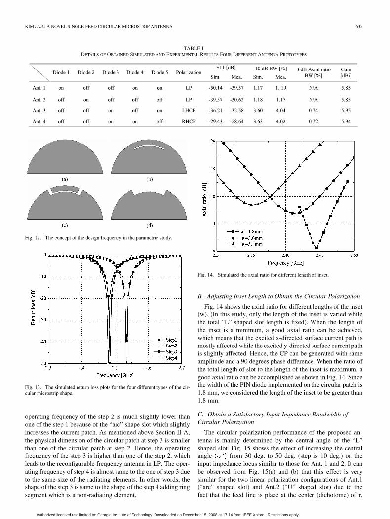
TABLE IDETAILS OF OBTAINED SIMULATED AND EXPERIMENTAL RESULTS FOUR DIFFERENT ANTENNA PROTOTYPES
Fig. 12. The concept of the design frequency in the parametric study.
Fig. 13. The simulated return loss plots for the four different types of the cir-cular microstrip shape.
operating frequency of the step 2 is much slightly lower thanone of the step 1 because of the “arc” shape slot which slightlyincreases the current patch. As mentioned above Section II-A,the physical dimension of the circular patch at step 3 is smallerthan one of the circular patch at step 2. Hence, the operatingfrequency of the step 3 is higher than one of the step 2, whichleads to the reconfigurable frequency antenna in LP. The oper-ating frequency of step 4 is almost same to the one of step 3 dueto the same size of the radiating elements. In other words, theshape of the step 3 is same to the shape of the step 4 adding ringsegment which is a non-radiating element.
Fig. 14. Simulated the axial ratio for different length of inset.
B. Adjusting Inset Length to Obtain the Circular Polarization
Fig. 14 shows the axial ratio for different lengths of the inset(w). (In this study, only the length of the inset is varied whilethe total “L” shaped slot length is fixed). When the length ofthe inset is a minimum, a good axial ratio can be achieved,which means that the excited x-directed surface current path ismostly affected while the excited y-directed surface current pathis slightly affected. Hence, the CP can be generated with sameamplitude and a 90 degrees phase difference. When the ratio ofthe total length of slot to the length of the inset is maximum, agood axial ratio can be accomplished as shown in Fig. 14. Sincethe width of the PIN diode implemented on the circular patch is1.8 mm, we considered the length of the inset to be greater than1.8 mm.
C. Obtain a Satisfactory Input Impedance Bandwidth ofCircular Polarization
The circular polarization performance of the proposed an-tenna is mainly determined by the central angle of the “L”shaped slot. Fig. 15 shows the effect of increasing the centralangle from 30 deg. to 50 deg. (step is 10 deg.) on theinput impedance locus similar to those for Ant. 1 and 2. It canbe observed from Fig. 15(a) and (b) that this effect is verysimilar for the two linear polarization configurations of Ant.1(“arc” shaped slot) and Ant.2 (“U” shaped slot) due to thefact that the feed line is place at the center (dichotome) of r.
Authorized licensed use limited to: Georgia Institute of Technology. Downloaded on December 15, 2008 at 17:14 from IEEE Xplore. Restrictions apply.

636 IEEE TRANSACTIONS ON ANTENNAS AND PROPAGATION, VOL. 56, NO. 3, MARCH 2008
Fig. 15. Simulated input impedance results for various angle of the slot. (a) “Arc” shape for Ant. 1. (b) “U” shape for Ant. 2. (c) “L” shape for Ant. 3.
Therefore, these two cases for Ant. 1 and 2 are observed forlinear polarization. Fig. 15(c) illustrates the impedance locusfor circular polarization. A good input impedance performanceis observed if the central angle is 40 for circular polarizationdue to the fact that the effective total “L” shaped slot lengthis approximately a quarter wavelength at given frequency.Hence, the impedance curve at 40 has the sharpness tip of thekink in the Smith chart enabling the best circular polarizationperformance. It has to be noted that the shape of this impedancecurve is a result of having two orthogonal modes with slightlydifferent resonant frequencies.
D. Adjusting to Obtain a Good Axial Ratio
After adjusting the central angle of the slot, the optimum axialratio that best characterizes circular polarization is investigatedby fine tuning the shifting angle which is defined as theangle between the midpoint on the “arc” shaped slot and theY-axis.
In the simulation, we adjust with the fixed length of the“arc” shaped slot to observe how beta could control the tip ofkink in input impedance locus which is directly related to theaxial ratio for circular polarization. Fig. 16 describes the varia-tion of the input impedance for Ant. 3 (CP) at different values ofangle . It is observed that a tip of the kink is sharper when
Fig. 16. Simulated the input impedance locus for varying shifting angle (� )of the “L” shape slot.
the shifting angle is 0 , because the excited x-directed (orthog-onal to the slot orientation) and the excited y-directed (parallel
Authorized licensed use limited to: Georgia Institute of Technology. Downloaded on December 15, 2008 at 17:14 from IEEE Xplore. Restrictions apply.
KIM et al.: A NOVEL SINGLE-FEED CIRCULAR MICROSTRIP ANTENNA 637
to the slot orientation) currents can constitute the optimum com-bination of the two-orthogonal-near-degenerate modes for thistopology.
V. CONCLUSION
The design of a novel single feed microstrip antenna with re-configurable polarization capabilities has been presented in thispaper. Unlike the conventional switchable polarizations studiedin past literature, the proposed antenna can be switched by con-trolling the PIN diodes for low frequency and high frequencymodes in linear polarization, as well as for LHCP and RHCPin circular polarization. A good impedance matching perfor-mance for all polarization senses is observed using open andshort stubs. All of the simulated and measured results agree verywell confirming the validity of our theory and the used models.By using the suitable switching devices (i.e., MEMS switch), theproposed antenna can be used in higher frequency commercialand military applications. It has to be noted that the proposedantenna design is desirable for many wireless communicationapplications such as wireless local area network (WLAN), satel-lite links, global positioning system (GPS) and space robots.
ACKNOWLEDGMENT
The authors would like to acknowledge the assistance fromDr. R. Li and G. DeJean.
REFERENCES
[1] F. Yang and Y. Rahmat-Samii, “A reconfigurable patch antenna usingswitchable slots for circular polarization diversity,” IEEE Microw.Wireless Comp. Lett., vol. 12, no. 3, pp. 96–98, Mar. 2002.
[2] M.-H. Ho, M.-T. Wu, C.-I. G. Hsu, and J.-Y. Sze, “An RHCP/LHCPswitchable slotline-fed slot-ring antenna,” Microw. Opt. Technol. Lett.,vol. 46, no. 1, pp. 30–33, Jul. 2005.
[3] H. Chuang, L. Kuo, C. Lin, and W. Chen, “A 2.4 GHz polarization-di-versity planar printed antenna for WLAN and wireless communicationsystems,” in Proc. IEEE Antennas and Propag. Society Int. Symp., Jun.2002, vol. 4, pp. 76–79.
[4] F. Yang and Y. Rahmat-Samii, “Patch antenna with switchable slots(PASS) in wireless communication: Concepts, designs, and applica-tions,” IEEE Trans. Antennas Propag., vol. 47, no. 2, Apr. 2005.
[5] M. K. Fries, M. Gräni, and R. Vahldieck, “A reconfigurable slot antennawith switchable polarization,” IEEE Microw. Wireless Compon. Lett.,vol. 13, no. 11, pp. 490–492, Nov. 2003.
[6] N. Jin, F. Yang, and Y. Rahmat-Samii, “A novel patch antenna withswitchable slot (PASS): Dual-frequency operation with reversed cir-cular polarizations,” IEEE Trans. Antennas Propag., vol. 54, no. 3, pp.1031–1034, Mar. 2006.
[7] M. Boti, L. Dussopt, and J.-M. Laheurte, “Circularly polarized antennawith switchable polarization sense,” Electron. Lett., vol. 36, no. 18, pp.1518–1519, Aug. 2000.
[8] Y. J. Sung, T. U. Jang, and Y.-S. Kim, “A reconfigurable microstripantenna for switchable polarization,” IEEE Microw. Wireless Compon.Lett., vol. 14, no. 11, pp. 534–536, Nov. 2004.
[9] S. Nikolaou, R. Bairavasubramanian, C. Lugo, I. Carrasquillo, D. C.Thompson, G. E. Ponchak, J. Papapolymerou, and M. M. Tentzeris,“Pattern and frequency reconfigurable annular slot antenna using PINdiodes,” IEEE Trans. Antennas Propag., vol. 54, no. 2, pp. 439–449,Feb. 2006.
[10] K. Chang, I. Bahl, and V. Nair, RF and Mircrowave Circuit and Com-ponent Design for Wireless Systems. New York: Wiley-Interscience,2002.
[11] Zeland’s IE3D 2004, Release 10.[12] D. M. Pozar, Microwave Engineering, 2nd ed. New York: Wiley,
1998.[13] Data Sheet of MA4P274CK PIN Diodes, , MA-Com, Application Note.
Boyon Kim (S’05) received the B.S. and M.S. de-grees from Korea University, Seoul, Korea, in 2003and 2007, respectively.
Since 2007, he has been an SoC Product and TestEngineer with System LSI Division, SemiconductorBusiness, Samsung Electronics Co., Ltd., Giheung,Korea, where he has been involved in RF Mobile PEand Test team. His research interests include Ultra-wideband (UWB) systems, orthogonal frequency di-vision multiplexing (OFDM), and developing the testmethods for mixed signal systems.
Bo Pan (S’03) received the B.S. and M.S. degreesfrom Tsinghua University, Beijing, China, in 2000and 2003, respectively. He is currently workingtoward the Ph.D. degree in electrical and computerengineering at the Georgia Institute of Technology,Atlanta.
His research involves the design, processing andcharacterization of novel micromachined passivecomponents for RF/Microwave/Millimeter-wavefront-ends. He is also researching antenna designsfor GPS/IMT-2000/WLAN/WiMAX applications.
Symeon Nikolaou received the Diploma in Electricaland Computer Engineering from the National Tech-nical University of Athens (NTUA), Athens, Greece,in 2003 and the M.S.E.C.E. and Ph.D. degrees fromGeorgia Institute of Technology, Atlanta, in 2005 and2007, respectively.
His current research interests include the designand development of compact UWB and reconfig-urable antennas, the development of RFIDs, and RFpackaging and design.
Young-Sik Kim (S’82–M’86) received the B.S. de-gree in electronics engineering from Korea Univer-sity, Seoul, in 1973, and the M.S. and Ph.D. degreesin electrical engineering from the University of Mass-achusetts at Amherst, in 1986 and 1988, respectively.
From 1988 to 1989, he was a Postdoctoral Re-search Fellow at the University of Massachusetts atAmherst. From 1989 to 1993, he was with the MobileCommunications Division, Korea Electronics andTelecommunications Research Institute, Daejeon.Since 1993, he has been with the Department of
Radio Sciences and Engineering, Korea University, where he is currently aProfessor. His main field of interest is millimeter-wave antennas and front-endsystems and mobile telecommunication systems.
John Papapolymerou (S’90–M’99–SM’04) re-ceived the B.S.E.E. degree from the NationalTechnical University of Athens, Athens, Greece, in1993, and the M.S.E.E. and Ph.D. degrees from theUniversity of Michigan, Ann Arbor, in 1994 and1999, respectively.
From 1999 to 2001, he was an Assistant Professorin the Department of Electrical and Computer Engi-neering, University of Arizona, Tucson, and duringsummers 2000 and 2003 he was a Visiting Professorat the University of Limoges, France. From 2001 to
2005, he was an Assistant Professor at the School of Electrical and ComputerEngineering, Georgia Institute of Technology (Georgia Tech), Atlanta, where heis currently an Associate Professor. His research interests include the implemen-tation of micromachining techniques and MEMS devices in microwave, mil-limeter-wave and THz circuits and the development of both passive and active
Authorized licensed use limited to: Georgia Institute of Technology. Downloaded on December 15, 2008 at 17:14 from IEEE Xplore. Restrictions apply.

638 IEEE TRANSACTIONS ON ANTENNAS AND PROPAGATION, VOL. 56, NO. 3, MARCH 2008
planar circuits on semiconductor (Si/SiGe, GaAs) and organic substrates (LCP,LTCC) for system-on-a-chip (SOC)/ system-on-a-package (SOP) RF front ends.He has authored or coauthored over 140 publications in peer reviewed journalsand conferences.
Dr. Papapolymerou received the 2004 Army Research Office (ARO) YoungInvestigator Award, the 2002 National Science Foundation (NSF) CAREERaward, the Best Paper Award at the 3rd IEEE International Conference Mi-crowave and Millimeter-Wave Technology (ICMMT2002), Beijing, China,and the 1997 Outstanding Graduate Student Instructional Assistant Award pre-sented by the American Society for Engineering Education (ASEE), Universityof Michigan Chapter. His student also received the Best Student Paper Award atthe 2004 IEEE Topical Meeting on Silicon Monolithic Integrated Circuits in RFSystems, Atlanta, GA. He currently serves as the Vice-Chair for CommissionD of the U.S. National Committee of the URSI and as an Associate Editor forthe IEEE MICROWAVE AND WIRELESS COMPONENT LETTERS and the IEEETRANSACTIONS ON ANTENNAS AND PROPAGATION. During 2004 he was theChair of the IEEE MTT/AP Atlanta Chapter.
Manos M. Tentzeris (S’89–M’98–SM’03) receivedthe Diploma Degree in Electrical and ComputerEngineering (magna cum laude) from the NationalTechnical University of Athens, Athens, Greeceand the M.S. and Ph.D. degrees in electrical engi-neering and computer science from the University ofMichigan, Ann Arbor.
He is currently an Associate Professor with Schoolof School of Electrical and Computer Engineering,Georgia Institute of Technology (Georgia Tech),Atlanta. He has published more than 260 papers
in refereed journals and conference proceedings, two books, and ten bookchapters. He has helped develop academic programs in highly integrated/multilayer packaging for RF and wireless applications using ceramic and or-ganic flexible materials, paper-based RFID’s and sensors, microwave MEM’s,SOP-integrated (UWB, multiband, conformal) antennas and adaptive numericalelectromagnetics (FDTD, multiresolution algorithms) and heads the ATHENAResearch Group, Georgia Tech, (20 researchers). He is the Georgia ElectronicDesign Center Associate Director for RFID/sensors research, and he has beenthe Georgia Tech NSF-Packaging Research Center Associate Director for RFResearch and the RF Alliance Leader from 2003–2006. He was a VisitingProfessor with the Technical University of Munich, Germany for summer 2002,where he introduced a course in the area of high-frequency packaging. He hasgiven more than 50 invited talks in the same area to various universities andcompanies in Europe, Asia, and America.
Dr. Tentzeris was the recipient/co-recipient of the 2007 IEEE APS Sympo-sium Best Student Paper Award, the 2007 IEEE IMS Third Best Student PaperAward, the 2007 ISAP 2007 Poster Presentation Award, the 2006 IEEE MTTOutstanding Young Engineer Award, the 2006 Asian-Pacific Microwave Confer-ence Award, the 2004 IEEE TRANSACTIONS ON ADVANCED PACKAGING Com-mendable Paper Award, the 2003 NASA Godfrey “Art” Anzic CollaborativeDistinguished Publication Award, the 2003 IBC International Educator of theYear Award, the 2003 IEEE CPMT Outstanding Young Engineer Award, the2002 International Conference Microwave and Millimeter-Wave TechnologyBest Paper Award (Beijing, China), the 2002 Georgia Tech-ECE OutstandingJunior Faculty Award, the 2001 ACES Conference Best Paper Award and the2000 NSF CAREER Award, and the 1997 Best Paper Award of the InternationalHybrid Microelectronics and Packaging Society. He was also the 1999 Tech-nical Program Co-Chair of the 54th ARFTG Conference, Atlanta, and the Chairof the 2005 IEEE CEM-TD Workshop. He is the Vice-Chair of the RF TechnicalCommittee (TC16) of the IEEE CPMT Society. He has organized various ses-sions and workshops on RF/Wireless Packaging and Integration, RFID’s, Nu-merical Techniques/Wavelets, in IEEE ECTC, IMS, VTC and APS Symposiain all of which he is a member of the Technical Program Committee in the areaof “Components and RF.” He will be the TPC Chair for IEEE IMS 2008 Sym-posium. He is an Associate Editor of the IEEE TRANSACTIONS ON ADVANCED
PACKAGING. He is a member of URSI Commission D, the MTT-15 Committee,an Associate Member of EuMA, a Fellow of the Electromagnetic Academy, anda member of the Technical Chamber of Greece.
Authorized licensed use limited to: Georgia Institute of Technology. Downloaded on December 15, 2008 at 17:14 from IEEE Xplore. Restrictions apply.