
5.1.5. Operation as vDS is Increased - UIC - Electrical ... · 5.1.5. Operation as v ... process...
7
5.1.5. Operation as v DS is Increased Q: What happens to i D when v DS increases beyond “small values”? A: The relationship between them ceases to be linear. Q: How can this non‐linearity be explained? step #1: Assume that v GS is held constant at value greater than V t . step #2: Also assume that v DS is applied and appears as voltage drop across n‐channel. step #3: Note that voltage decreases from v GS at the source end of channel to v GD at drain end, where… v GD = v GS – v DS v GD = V t + v OV – v DS
Transcript of 5.1.5. Operation as vDS is Increased - UIC - Electrical ... · 5.1.5. Operation as v ... process...
Oxford University PublishingMicroelectronic Circuits by Adel S. Sedra and Kenneth C. Smith (0195323033)
5.1.5. Operation as vDS is Increased
Q:What happens to iD when vDS increases beyond “small values”? A: The relationship between them ceases to be linear.
Q: How can this non‐linearity be explained? step #1: Assume that vGS is held constant at value greater than Vt.
step #2: Also assume that vDS is applied and appears as voltage drop across n‐channel.
step #3: Note that voltage decreases from vGS at the source end of channel to vGD at drain end, where… vGD = vGS – vDS vGD = Vt + vOV – vDS
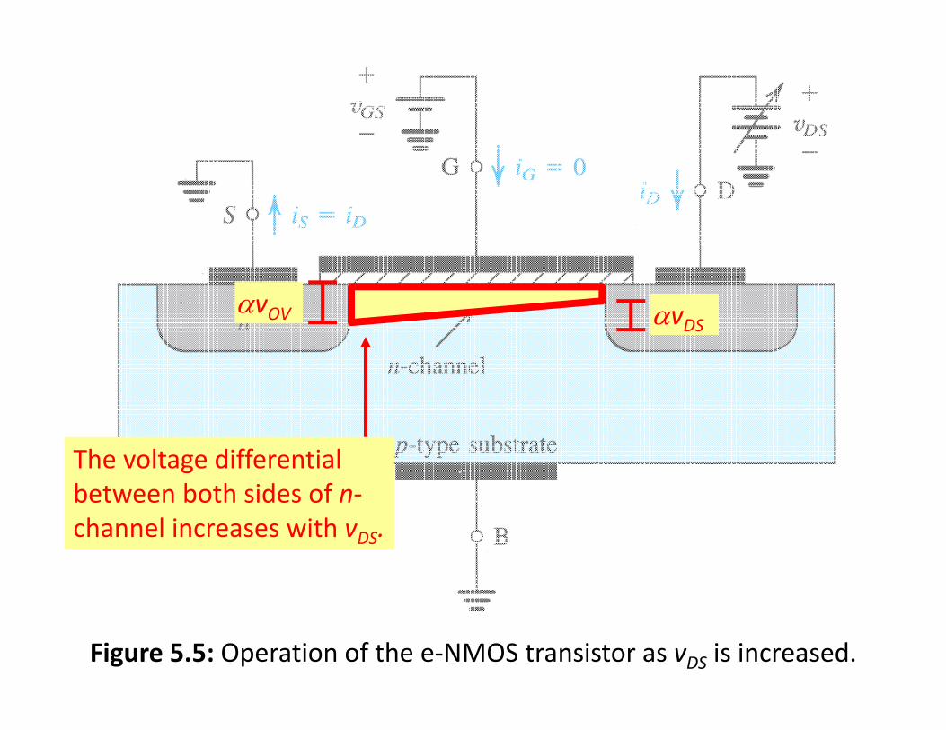
Oxford University PublishingMicroelectronic Circuits by Adel S. Sedra and Kenneth C. Smith (0195323033)Figure 5.5: Operation of the e‐NMOS transistor as vDS is increased.
vDSvOV
The voltage differential between both sides of n‐channel increases with vDS.

Oxford University PublishingMicroelectronic Circuits by Adel S. Sedra and Kenneth C. Smith (0195323033)
Figure 5.6(a): For a MOSFET with vGS = Vt + vOV application of vDS causes the voltage drop along the channel to vary linearly, with an average value of vDS at the midpoint. Since vGD > Vt, the channel still exists at the drain end. (b) The channel shape corresponding to the situation in (a). While the depth of
the channel at the source is still proportional to vOV, the drain end is not.
note the average value note that we can define total charge stored in channel |Q|
as area of this trapezoid
12OV DSQ v v L

Oxford University PublishingMicroelectronic Circuits by Adel S. Sedra and Kenneth C. Smith (0195323033)
Q: How can this non‐linearity be explained?
step #4: Define iDSin terms of vDSand vOV.
12
if then
12
repl
12
1
ace w
2
ith
(eq5.7)
if
ot(eq5.7)
herwise
(eq5.1 4)
DS OV
OV O
D
V D
S O
S
V
DS OV
v v
D n ox OV DS DS
n ox OV DS DS
n ox OV DS
v v
D
v
v
DS
v
Wi C v v v
L
WC v v vv v
LW
C vi
v vL
action:
12
2
1
if in
otherwise2
n ox OV DS DS
D
n O
DS OV
ox V
vW
C v v vLiC
L
vA
Wv
triode vs. saturation region
iD is dependent on the apparent vOV (not vDS
inherently) which does not change after vDS > vOV
Oxford University PublishingMicroelectronic Circuits by Adel S. Sedra and Kenneth C. Smith (0195323033)
12
2
if (eq5.14) in
othe
triode:
saturation:
1
s2
rwi e
DS On ox OV DS DS
D
n O
V
ox V
WC v v v
LW
C vL
vi
vA
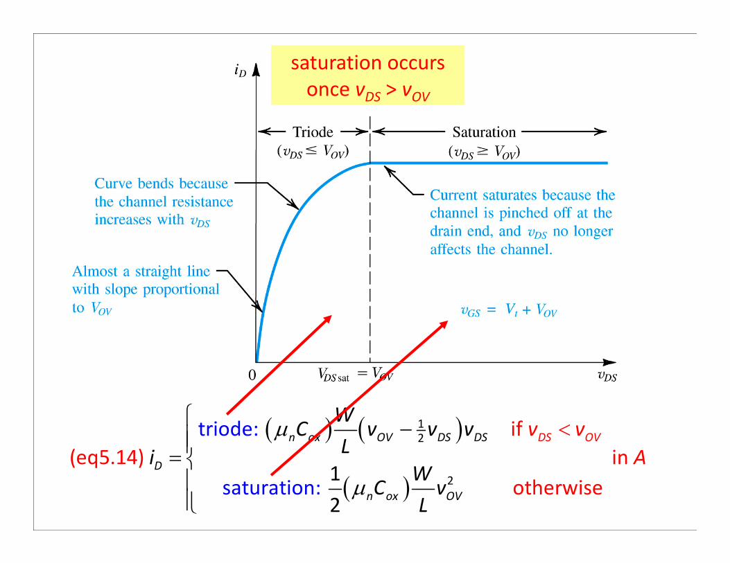
saturation occurs once vDS > vOV

Oxford University PublishingMicroelectronic Circuits by Adel S. Sedra and Kenneth C. Smith (0195323033)
5.1.6. Operation for vDS >> vOV
In section 5.1.5, we assume that n‐channel is tapered but channel pinch‐off does not occur. Trapezoid doesn’t become triangle for vGD > Vt
Q:What happens if vDS > vOV? A:MOSFET enters saturation region. Any further increase in vDS has no effect on iD.
Figure 5.8: Operation of MOSFET with vGS = Vt + vOV as vDS is increased to vOV. At the drain end, vGD decreases to Vt and the channel depth at the drain‐end reduces to zero (pinch‐off). At this point, the MOSFET enters saturation more of operation. Further increasing vDS (beyond vOV) has no effect on the channel shape and iD
remains constant.
pinch‐off does not mean blockage of current

Oxford University PublishingMicroelectronic Circuits by Adel S. Sedra and Kenneth C. Smith (0195323033)
Example 5.1: NMOS MOSFET
Example 5.1. Problem Statement: Consider an NMOS process technology for which Lmin = 0.4m, tox = 8nm, n = 450cm2/Vs, Vt = 0.7V.
Q(a): Find Cox and k’n. Q(b): For a MOSFET with W/L = 8m/0.8m, calculate the
values of vOV, vGS, and vDSmin needed to operate the transistor in the saturation region with dc current ID = 100A.
Q(c): For the device in (b), find the values of vOV and vGSrequired to cause the device to operate as a 1000ohmresistor for very small vDS.


![[MS-VDS-Diff]: Virtual Disk Service (VDS) Protocol · 3 / 349 [MS-VDS-Diff] - v20170601 Virtual Disk Service (VDS) Protocol Copyright © 2017 Microsoft Corporation Release: June 1,](https://static.fdocuments.in/doc/165x107/5ece115ec9f8163d2d78ee85/ms-vds-diff-virtual-disk-service-vds-protocol-3-349-ms-vds-diff-v20170601.jpg)


![[MS-VDS]: Virtual Disk Service (VDS) Protocol... · [MS-VDS]: Virtual Disk Service (VDS) Protocol Intellectual Property Rights Notice for Open Specifications Documentation](https://static.fdocuments.in/doc/165x107/5ece0e4751b19024473b3e8c/ms-vds-virtual-disk-service-vds-protocol-ms-vds-virtual-disk-service.jpg)


