50mA Wireless Charger Booster Pack - TI.com · 1 Key System Specifications . ... 3.49 Vdc VIN_OK on...
25
TI Design: TIDA-00688 50mA Wireless Charger Booster Pack TI Designs TI Designs provide the foundation that you need including methodology, testing and design files to quickly evaluate and customize the system. TI Designs help you accelerate your time to market. Design Resources TIDA-00668 Design Folder bq51003 Product Folder bq25100 Product Folder bq29707 Product Folder TPS62736 Product Folder Block Diagram bq51003 Wireless RX bq25100 Charger TPS61220 5V boost TPS62736 3.3V buck bq29707 Protection H e a d e r H e a d e r 5V 3.3V 3.6V Li-Ion Coin Cell ADC_IN VIN_OK Coil Design Features Wireless Charger Booster Pack designed for any low power Launchpad Coin Cell storage to 50mA Qi Compatible - Recharge the battery from any Qi transmitter 3.3Vdc buck to power the Launchpad 5V boost to power support circuitry Stackable design allows for creating a complete solution Featured Applications • Factory Automation and Process Control • Sensors and Field Transmitters • Building Automation • Portable Instruments • IoT (Internet of Things) • Wearables Board Image TIDUAN3 - September 2015 50mA Wireless Charger Booster Pack Copyright © 2015, Texas Instruments Incorporated Ask The Analog Experts WEBENCH® Design Center
Transcript of 50mA Wireless Charger Booster Pack - TI.com · 1 Key System Specifications . ... 3.49 Vdc VIN_OK on...
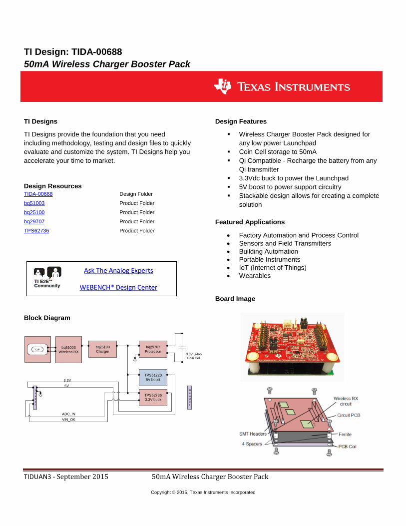
TI Design: TIDA-00688 50mA Wireless Charger Booster Pack
TI Designs
TI Designs provide the foundation that you need including methodology, testing and design files to quickly evaluate and customize the system. TI Designs help you accelerate your time to market.
Design Resources TIDA-00668 Design Folder
bq51003 Product Folder
bq25100 Product Folder
bq29707 Product Folder
TPS62736 Product Folder
Block Diagram
bq51003Wireless RX
bq25100Charger
TPS612205V boost
TPS627363.3V buck
bq29707Protection
Header
Header
5V3.3V
3.6V Li-Ion Coin Cell
ADC_INVIN_OK
Coil
Design Features
Wireless Charger Booster Pack designed for any low power Launchpad
Coin Cell storage to 50mA Qi Compatible - Recharge the battery from any
Qi transmitter 3.3Vdc buck to power the Launchpad 5V boost to power support circuitry Stackable design allows for creating a complete
solution
Featured Applications
• Factory Automation and Process Control • Sensors and Field Transmitters • Building Automation • Portable Instruments • IoT (Internet of Things) • Wearables
Board Image
TIDUAN3 - September 2015 50mA Wireless Charger Booster Pack
Copyright © 2015, Texas Instruments Incorporated
Ask The Analog Experts
WEBENCH® Design Center
www.ti.com
TIDUAN3 - September 2015 50mA Wireless Charger Booster Pack 2
Copyright © 2015, Texas Instruments Incorporated
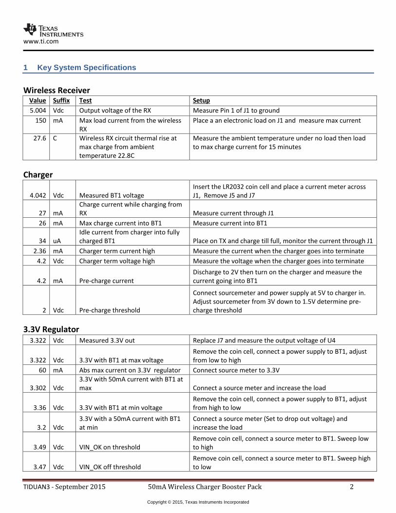
1 Key System Specifications Wireless Receiver
Value Suffix Test Setup 5.004 Vdc Output voltage of the RX Measure Pin 1 of J1 to ground
150 mA Max load current from the wireless RX
Place a an electronic load on J1 and measure max current
27.6 C Wireless RX circuit thermal rise at max charge from ambient temperature 22.8C
Measure the ambient temperature under no load then load to max charge current for 15 minutes
Charger
4.042 Vdc Measured BT1 voltage Insert the LR2032 coin cell and place a current meter across J1, Remove J5 and J7
27 mA Charge current while charging from RX Measure current through J1
26 mA Max charge current into BT1 Measure current into BT1
34 uA Idle current from charger into fully charged BT1 Place on TX and charge till full, monitor the current through J1
2.36 mA Charger term current high Measure the current when the charger goes into terminate 4.2 Vdc Charger term voltage high Measure the voltage when the charger goes into terminate
4.2 mA Pre-charge current Discharge to 2V then turn on the charger and measure the current going into BT1
2 Vdc Pre-charge threshold
Connect sourcemeter and power supply at 5V to charger in. Adjust sourcemeter from 3V down to 1.5V determine pre-charge threshold
3.3V Regulator
3.322 Vdc Measured 3.3V out Replace J7 and measure the output voltage of U4
3.322 Vdc 3.3V with BT1 at max voltage Remove the coin cell, connect a power supply to BT1, adjust from low to high
60 mA Abs max current on 3.3V regulator Connect source meter to 3.3V
3.302 Vdc 3.3V with 50mA current with BT1 at max Connect a source meter and increase the load
3.36 Vdc 3.3V with BT1 at min voltage Remove the coin cell, connect a power supply to BT1, adjust from high to low
3.2 Vdc 3.3V with a 50mA current with BT1 at min
Connect a source meter (Set to drop out voltage) and increase the load
3.49 Vdc VIN_OK on threshold Remove coin cell, connect a source meter to BT1. Sweep low to high
3.47 Vdc VIN_OK off threshold Remove coin cell, connect a source meter to BT1. Sweep high to low
www.ti.com
TIDUAN3 - September 2015 50mA Wireless Charger Booster Pack 3
Copyright © 2015, Texas Instruments Incorporated
0 Vdc 3.3V disable Remove J7 measure output of 3.3V regulator
23.6 C 3.3V circuit thermal rise at 50mA (22.8C ambient)
Measure the ambient temperature under no load then load to max current for 15 minutes with BT1 at min
5V Regulator
5.031 Vdc Measured 5V out Replace J5 and measure the output voltage of U3
5.0249 Vdc 5V with BT1 at max voltage Remove the coin cell, connect a power supply to BT1, adjust from low to high
5.021 Vdc 5V with BT1 at min voltage Remove the coin cell, connect a power supply to BT1, adjust from high to low
5.072 Vdc 5V with 50mA current with BT1 at min voltage Connect a source meter and increase the load
5.051 Vdc 5V with 50mA current with BT1 at max voltage Connect a source meter and increase the load
75 mA Abs max current on 5V regulator Connect source meter to 5V
3.57 Vdc 5V disable (Input voltage minus forward diode drop when off) Remove J5 measure output of 5V regulator
23.4 C 5V circuit thermal rise at 50mA (22.8C ambient)
measure the ambient temperature under no load then load to max current for 15 minutes with BT1 at min
Protector
4.29 Vdc Protection voltage max Remove coin cell, connect a source meter to BT1. Sweep low to high
2.79 Vdc Protection voltage min Remove coin cell, connect a source meter to BT1. Sweep high to low
102 mA Protection current
Remove coin cell, connect a power supply to BT1, connect source meter to 5V and increase the load thru the protection circuit to test max current
System
2.0058 mV Measure ADC_IN ADC_IN voltage ~1/2 of BT1 (loaded network from 1Meg multi-meter impedance)
31 uA quiescent current of total circuit no load
measure the current from the battery to support all of the circuits
www.ti.com
TIDUAN3 - September 2015 50mA Wireless Charger Booster Pack 4
Copyright © 2015, Texas Instruments Incorporated
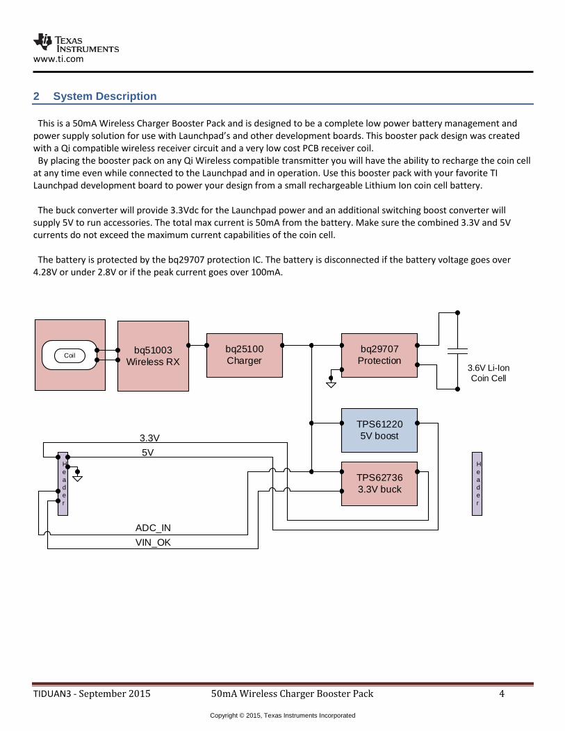
2 System Description This is a 50mA Wireless Charger Booster Pack and is designed to be a complete low power battery management and power supply solution for use with Launchpad’s and other development boards. This booster pack design was created with a Qi compatible wireless receiver circuit and a very low cost PCB receiver coil. By placing the booster pack on any Qi Wireless compatible transmitter you will have the ability to recharge the coin cell at any time even while connected to the Launchpad and in operation. Use this booster pack with your favorite TI Launchpad development board to power your design from a small rechargeable Lithium Ion coin cell battery. The buck converter will provide 3.3Vdc for the Launchpad power and an additional switching boost converter will supply 5V to run accessories. The total max current is 50mA from the battery. Make sure the combined 3.3V and 5V currents do not exceed the maximum current capabilities of the coin cell. The battery is protected by the bq29707 protection IC. The battery is disconnected if the battery voltage goes over 4.28V or under 2.8V or if the peak current goes over 100mA.
bq51003Wireless RX
bq25100Charger
TPS612205V boost
TPS627363.3V buck
bq29707Protection
Header
Header
5V3.3V
3.6V Li-Ion Coin Cell
ADC_INVIN_OK
Coil
www.ti.com
TIDUAN3 - September 2015 50mA Wireless Charger Booster Pack 5
Copyright © 2015, Texas Instruments Incorporated
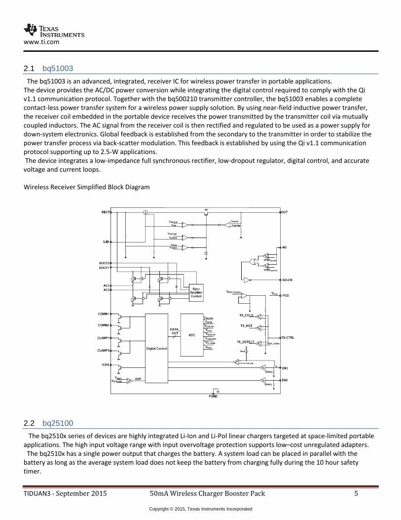
2.1 bq51003 The bq51003 is an advanced, integrated, receiver IC for wireless power transfer in portable applications. The device provides the AC/DC power conversion while integrating the digital control required to comply with the Qi v1.1 communication protocol. Together with the bq500210 transmitter controller, the bq51003 enables a complete contact-less power transfer system for a wireless power supply solution. By using near-field inductive power transfer, the receiver coil embedded in the portable device receives the power transmitted by the transmitter coil via mutually coupled inductors. The AC signal from the receiver coil is then rectified and regulated to be used as a power supply for down-system electronics. Global feedback is established from the secondary to the transmitter in order to stabilize the power transfer process via back-scatter modulation. This feedback is established by using the Qi v1.1 communication protocol supporting up to 2.5-W applications. The device integrates a low-impedance full synchronous rectifier, low-dropout regulator, digital control, and accurate voltage and current loops. Wireless Receiver Simplified Block Diagram
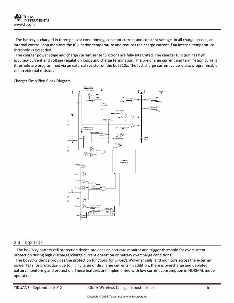
2.2 bq25100 The bq2510x series of devices are highly integrated Li-Ion and Li-Pol linear chargers targeted at space-limited portable applications. The high input voltage range with input overvoltage protection supports low–cost unregulated adapters. The bq2510x has a single power output that charges the battery. A system load can be placed in parallel with the battery as long as the average system load does not keep the battery from charging fully during the 10 hour safety timer.
www.ti.com
TIDUAN3 - September 2015 50mA Wireless Charger Booster Pack 6
Copyright © 2015, Texas Instruments Incorporated
The battery is charged in three phases: conditioning, constant current and constant voltage. In all charge phases, an internal control loop monitors the IC junction temperature and reduces the charge current if an internal temperature threshold is exceeded. The charger power stage and charge current sense functions are fully integrated. The charger function has high accuracy current and voltage regulation loops and charge termination. The pre-charge current and termination current threshold are programmed via an external resistor on the bq2510x. The fast charge current value is also programmable via an external resistor. Charger Simplified Block Diagram
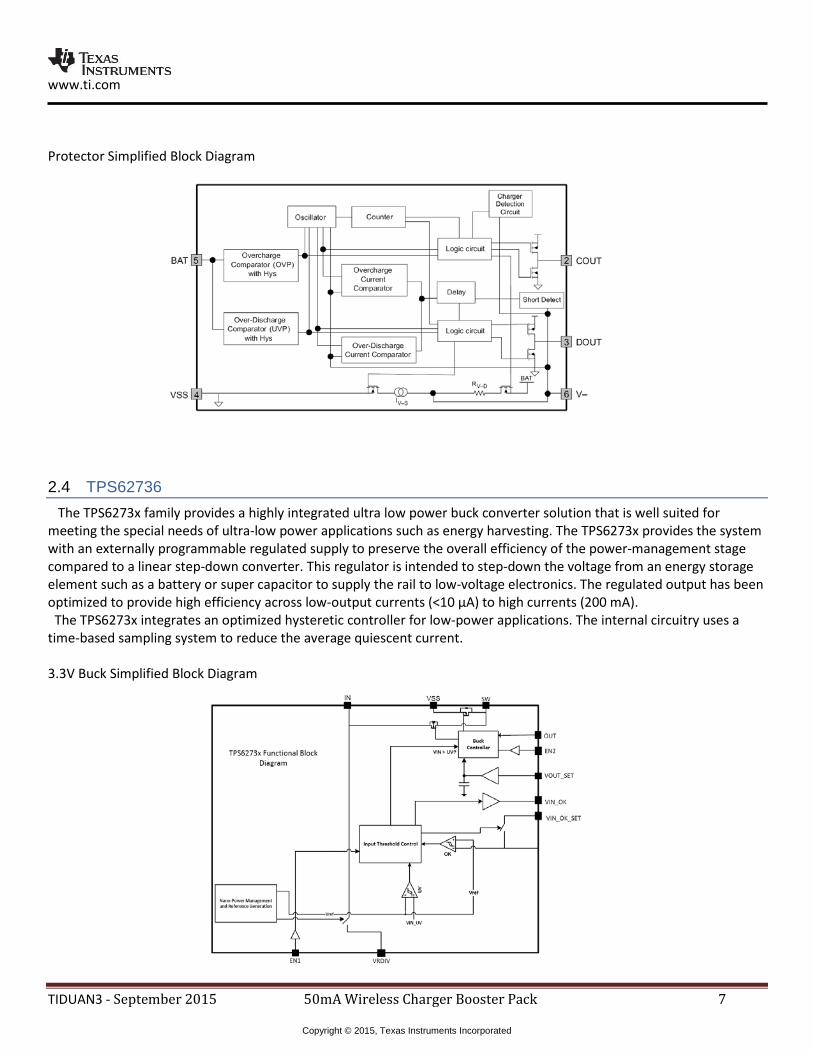
2.3 bq29707 The bq297xy battery cell protection device provides an accurate monitor and trigger threshold for overcurrent protection during high discharge/charge current operation or battery overcharge conditions. The bq297xy device provides the protection functions for Li-Ion/Li-Polymer cells, and monitors across the external power FETs for protection due to high charge or discharge currents. In addition, there is overcharge and depleted battery monitoring and protection. These features are implemented with low current consumption in NORMAL mode operation.
www.ti.com
TIDUAN3 - September 2015 50mA Wireless Charger Booster Pack 7
Copyright © 2015, Texas Instruments Incorporated
Protector Simplified Block Diagram
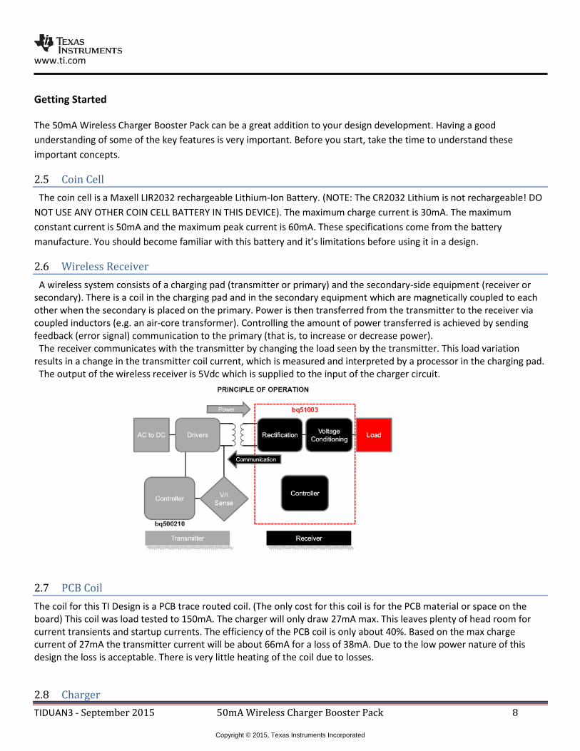
2.4 TPS62736 The TPS6273x family provides a highly integrated ultra low power buck converter solution that is well suited for meeting the special needs of ultra-low power applications such as energy harvesting. The TPS6273x provides the system with an externally programmable regulated supply to preserve the overall efficiency of the power-management stage compared to a linear step-down converter. This regulator is intended to step-down the voltage from an energy storage element such as a battery or super capacitor to supply the rail to low-voltage electronics. The regulated output has been optimized to provide high efficiency across low-output currents (<10 μA) to high currents (200 mA). The TPS6273x integrates an optimized hysteretic controller for low-power applications. The internal circuitry uses a time-based sampling system to reduce the average quiescent current. 3.3V Buck Simplified Block Diagram
www.ti.com
TIDUAN3 - September 2015 50mA Wireless Charger Booster Pack 8
Copyright © 2015, Texas Instruments Incorporated
Getting Started The 50mA Wireless Charger Booster Pack can be a great addition to your design development. Having a good understanding of some of the key features is very important. Before you start, take the time to understand these important concepts.
2.5 Coin Cell The coin cell is a Maxell LIR2032 rechargeable Lithium-Ion Battery. (NOTE: The CR2032 Lithium is not rechargeable! DO NOT USE ANY OTHER COIN CELL BATTERY IN THIS DEVICE). The maximum charge current is 30mA. The maximum constant current is 50mA and the maximum peak current is 60mA. These specifications come from the battery manufacture. You should become familiar with this battery and it’s limitations before using it in a design.
2.6 Wireless Receiver A wireless system consists of a charging pad (transmitter or primary) and the secondary-side equipment (receiver or secondary). There is a coil in the charging pad and in the secondary equipment which are magnetically coupled to each other when the secondary is placed on the primary. Power is then transferred from the transmitter to the receiver via coupled inductors (e.g. an air-core transformer). Controlling the amount of power transferred is achieved by sending feedback (error signal) communication to the primary (that is, to increase or decrease power). The receiver communicates with the transmitter by changing the load seen by the transmitter. This load variation results in a change in the transmitter coil current, which is measured and interpreted by a processor in the charging pad. The output of the wireless receiver is 5Vdc which is supplied to the input of the charger circuit.
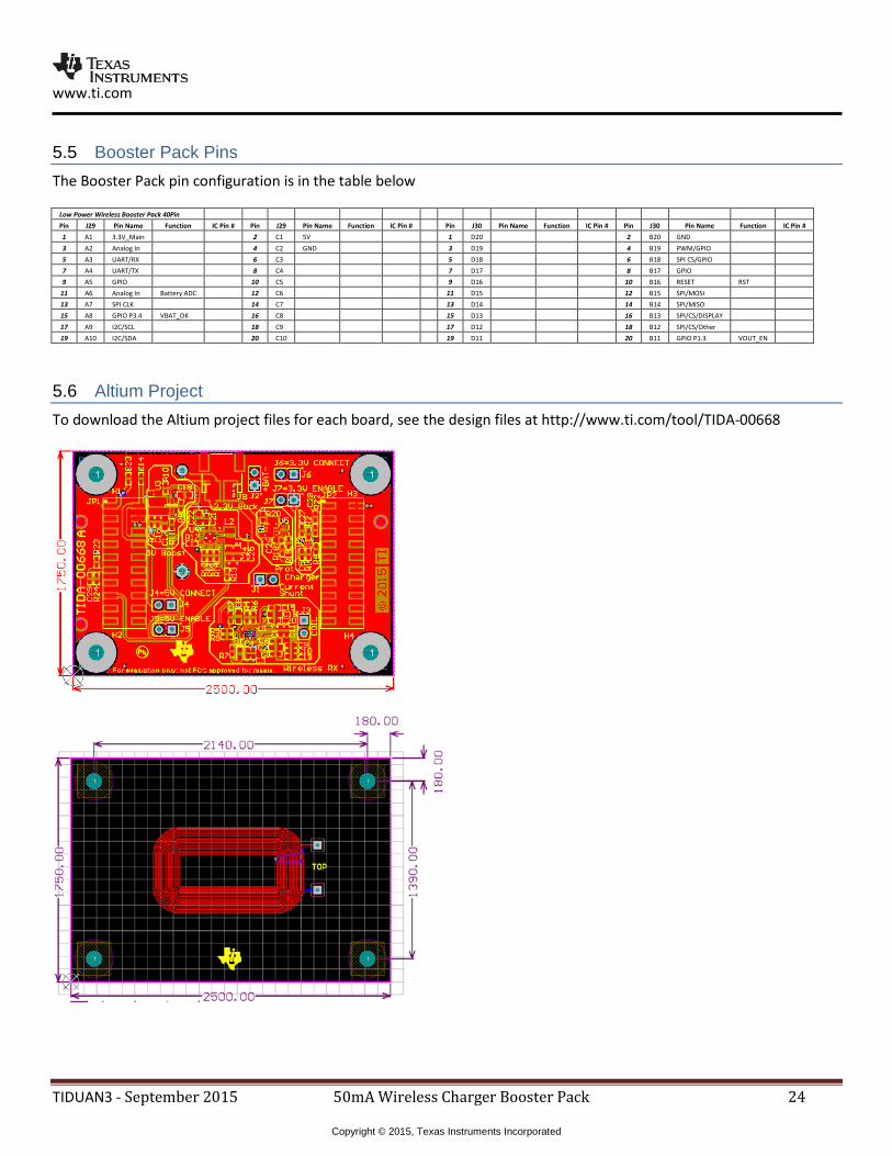
2.7 PCB Coil The coil for this TI Design is a PCB trace routed coil. (The only cost for this coil is for the PCB material or space on the board) This coil was load tested to 150mA. The charger will only draw 27mA max. This leaves plenty of head room for current transients and startup currents. The efficiency of the PCB coil is only about 40%. Based on the max charge current of 27mA the transmitter current will be about 66mA for a loss of 38mA. Due to the low power nature of this design the loss is acceptable. There is very little heating of the coil due to losses.
2.8 Charger
www.ti.com
TIDUAN3 - September 2015 50mA Wireless Charger Booster Pack 9
Copyright © 2015, Texas Instruments Incorporated
2.9 External Battery The use of an external battery is possible with the external battery connector supplied on the board. There are a few design concerns when using an external battery. First it is the responsibility of the designer to make sure that all safety precautions are met for your design. The max charge current from the bq25100 is 250mA and the max charge voltage is 4.2Vdc. The Wireless receiver can supply currents greater than the 250mA but not with the attached coil. It’s up to the user to select a proper coil, modify the parallel and series capacitors as required, change the current limit of the wireless receiver, change the charger current limit and the protection current limit if it desired to use this circuit at a higher current. With an external battery with a C-Rate above 200mAh the 3.3V regulator and the 5V regulator can supply up to 100mA each. It is possible to use a larger battery without changing the circuit board. Your battery will charge at 26mA.
2.10 3.3V and 5.0V regulators This design has a 3.3V buck regulator. The output voltage is resister programmed for 3.3Vdc. The regulator can supply up to 100mA of current, however the coin cell can only supply 50mA, so it is up to the user to make sure that there circuit does not draw more than the maximum current that the battery can supply. The 3.3Vdc buck will not turn on until the VBAT reaches 3.5Vdc. The 5V regulator is a boost circuit. It runs off of the coin cell. The regulator will operate down to the 2.8V cutoff of the protector. The output voltage of the boost regulator is resister programmable and is set to 5.00V. The max output current is 70mA. Because this is a boost converter the input current will always be higher than the output. At about 3V input the current will be high enough to limit the output current to about 30mA. Do not plan to use more than the 30mA or the protector will disconnect the battery for over current.
2.11 Charger The bq2510x is a highly integrated family of single cell Li-Ion and Li-Pol chargers. The charger can be used to charge a battery, power a system or both. The charger has three phases of charging: pre-charge to recover a fully discharged battery, fast-charge constant current to supply the charge safely and voltage regulation to safely reach full capacity. The charger is very flexible, allowing programming of the fast-charge current and Pre-charge/Termination Current. The charger runs on the 5V input from the wireless receiver. The output current of the charger is set to about 26mA and a pre-charge of about 4mA. The termination current is about 2mA. All of this is resister programmable and can be changed if needed.
2.12 Protection This bq29707 device is a primary protector for a single-cell Li-Ion/Li-Polymer battery pack. The device uses a minimum number of external components to protect for overcurrent conditions due to high discharge/charge currents in the application. In addition, it monitors and helps to protect against battery pack overcharging or depletion of energy in the pack. See the chart below for the functional levels of protection.
In the condition when a fault is triggered, there are timer delays before the appropriate action is taken to turn OFF either the CHG or DSG FETs. There is also a timer delay for the recovery period once the threshold for recovery condition is satisfied. There is also a feature called zero voltage charging that enables depleted cells to be charged to a acceptable level before the battery pack can be used for normal operation. Zero voltage charging is allowed if the charger voltage is above 1.7 V.
www.ti.com
TIDUAN3 - September 2015 50mA Wireless Charger Booster Pack 10
Copyright © 2015, Texas Instruments Incorporated
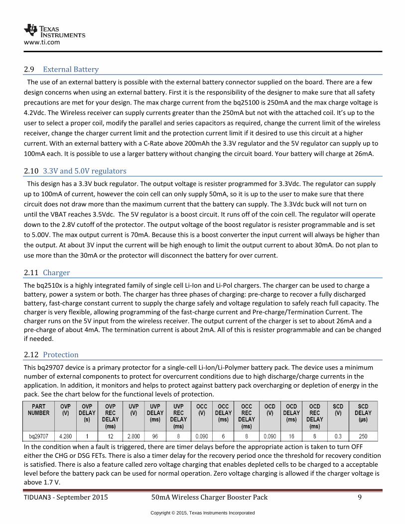
When the battery is connected for the first time, the discharging circuit may not be enabled. In this case, short the V– pin to the VSS pin. Reference the two green arrows on the board. Alternatively, set the unit on a wireless transmitter.
2.13 Jumpers This section will help the user to set up and configure the wireless charger booster pack for basic and custom applications
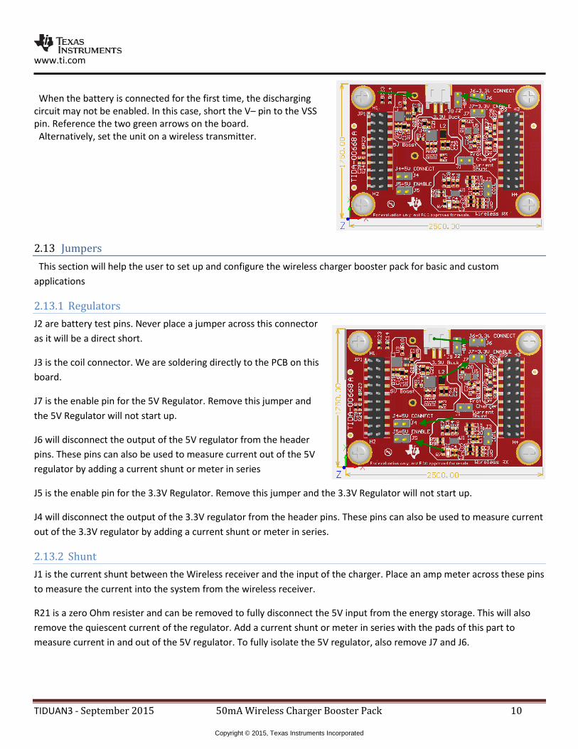
2.13.1 Regulators J2 are battery test pins. Never place a jumper across this connector as it will be a direct short.
J3 is the coil connector. We are soldering directly to the PCB on this board.
J7 is the enable pin for the 5V Regulator. Remove this jumper and the 5V Regulator will not start up.
J6 will disconnect the output of the 5V regulator from the header pins. These pins can also be used to measure current out of the 5V regulator by adding a current shunt or meter in series
J5 is the enable pin for the 3.3V Regulator. Remove this jumper and the 3.3V Regulator will not start up.
J4 will disconnect the output of the 3.3V regulator from the header pins. These pins can also be used to measure current out of the 3.3V regulator by adding a current shunt or meter in series.
2.13.2 Shunt J1 is the current shunt between the Wireless receiver and the input of the charger. Place an amp meter across these pins to measure the current into the system from the wireless receiver.
R21 is a zero Ohm resister and can be removed to fully disconnect the 5V input from the energy storage. This will also remove the quiescent current of the regulator. Add a current shunt or meter in series with the pads of this part to measure current in and out of the 5V regulator. To fully isolate the 5V regulator, also remove J7 and J6.
www.ti.com
TIDUAN3 - September 2015 50mA Wireless Charger Booster Pack 11
Copyright © 2015, Texas Instruments Incorporated
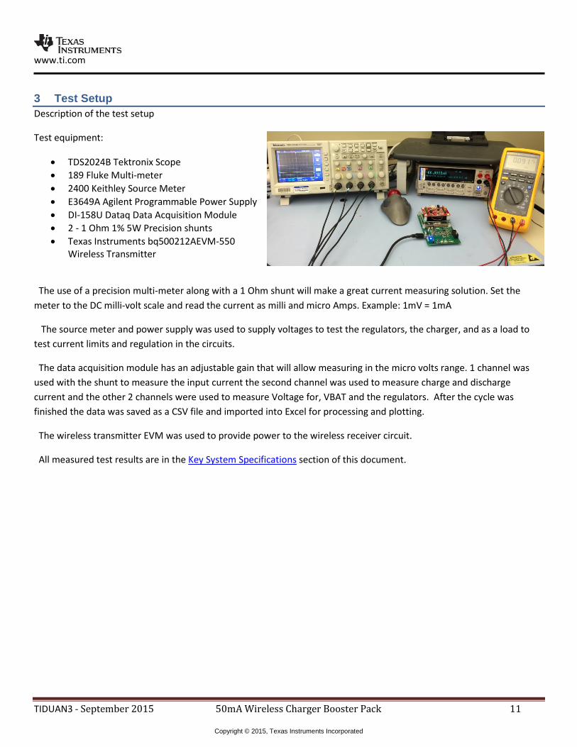
3 Test Setup Description of the test setup
Test equipment:
• TDS2024B Tektronix Scope • 189 Fluke Multi-meter • 2400 Keithley Source Meter • E3649A Agilent Programmable Power Supply • DI-158U Dataq Data Acquisition Module • 2 - 1 Ohm 1% 5W Precision shunts • Texas Instruments bq500212AEVM-550
Wireless Transmitter
The use of a precision multi-meter along with a 1 Ohm shunt will make a great current measuring solution. Set the meter to the DC milli-volt scale and read the current as milli and micro Amps. Example: 1mV = 1mA
The source meter and power supply was used to supply voltages to test the regulators, the charger, and as a load to test current limits and regulation in the circuits.
The data acquisition module has an adjustable gain that will allow measuring in the micro volts range. 1 channel was used with the shunt to measure the input current the second channel was used to measure charge and discharge current and the other 2 channels were used to measure Voltage for, VBAT and the regulators. After the cycle was finished the data was saved as a CSV file and imported into Excel for processing and plotting.
The wireless transmitter EVM was used to provide power to the wireless receiver circuit.
All measured test results are in the Key System Specifications section of this document.
www.ti.com
TIDUAN3 - September 2015 50mA Wireless Charger Booster Pack 12
Copyright © 2015, Texas Instruments Incorporated
4 Test Data The following description explains the test plots and scope captures that
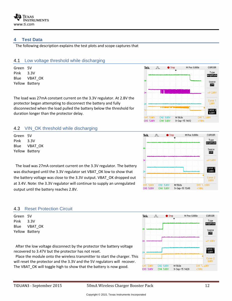
4.1 Low voltage threshold while discharging Green 5V Pink 3.3V Blue VBAT_OK Yellow Battery
The load was 27mA constant current on the 3.3V regulator. At 2.8V the protector began attempting to disconnect the battery and fully disconnected when the load pulled the battery below the threshold for duration longer than the protector delay.
4.2 VIN_OK threshold while discharging Green 5V Pink 3.3V Blue VBAT_OK Yellow Battery
The load was 27mA constant current on the 3.3V regulator. The battery was discharged until the 3.3V regulator set VBAT_OK low to show that the battery voltage was close to the 3.3V output. VBAT_OK dropped out at 3.4V. Note: the 3.3V regulator will continue to supply an unregulated output until the battery reaches 2.8V.
4.3 Reset Protection Circuit Green 5V Pink 3.3V Blue VBAT_OK Yellow Battery
After the low voltage disconnect by the protector the battery voltage recovered to 3.47V but the protector has not reset. Place the module onto the wireless transmitter to start the charger. This will reset the protector and the 3.3V and the 5V regulators will recover. The VBAT_OK will toggle high to show that the battery is now good.
www.ti.com
TIDUAN3 - September 2015 50mA Wireless Charger Booster Pack 13
Copyright © 2015, Texas Instruments Incorporated
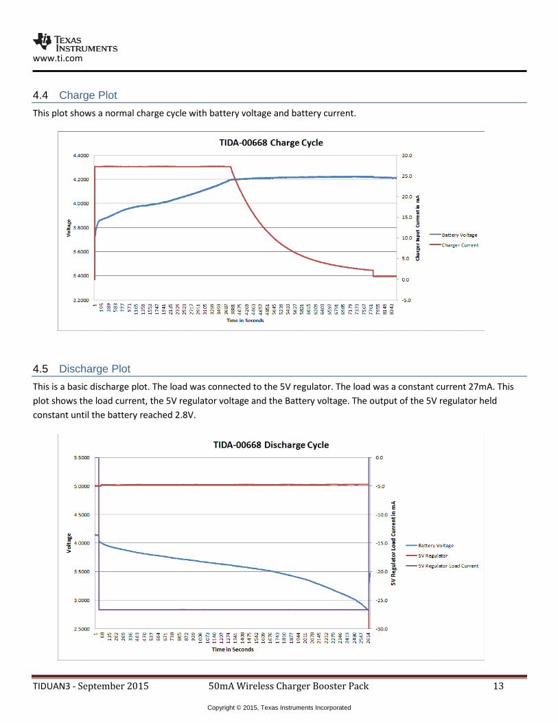
4.4 Charge Plot This plot shows a normal charge cycle with battery voltage and battery current.
4.5 Discharge Plot This is a basic discharge plot. The load was connected to the 5V regulator. The load was a constant current 27mA. This plot shows the load current, the 5V regulator voltage and the Battery voltage. The output of the 5V regulator held constant until the battery reached 2.8V.
www.ti.com
TIDUAN3 - September 2015 50mA Wireless Charger Booster Pack 14
Copyright © 2015, Texas Instruments Incorporated
5 Design Files
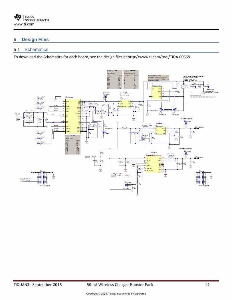
5.1 Schematics To download the Schematics for each board, see the design files at http://www.ti.com/tool/TIDA-00668
www.ti.com
TIDUAN3 - September 2015 50mA Wireless Charger Booster Pack 15
Copyright © 2015, Texas Instruments Incorporated
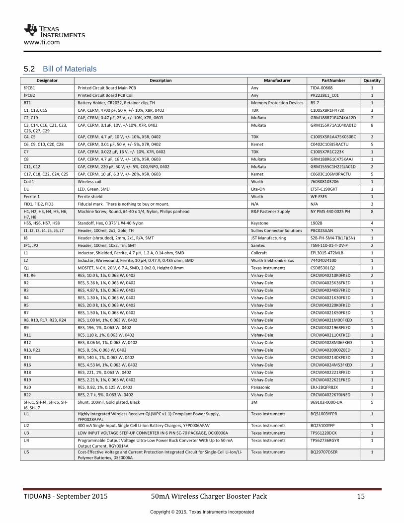
5.2 Bill of Materials Designator Description Manufacturer PartNumber Quantity
!PCB1 Printed Circuit Board Main PCB Any TIDA-00668 1
!PCB2 Printed Circuit Board PCB Coil Any PR2228E1_C01 1
BT1 Battery Holder, CR2032, Retainer clip, TH Memory Protection Devices BS-7 1
C1, C13, C15 CAP, CERM, 4700 pF, 50 V, +/- 10%, X8R, 0402 TDK C1005X8R1H472K 3
C2, C19 CAP, CERM, 0.47 µF, 25 V, +/- 10%, X7R, 0603 MuRata GRM188R71E474KA12D 2
C3, C14, C16, C21, C23, C26, C27, C29
CAP, CERM, 0.1uF, 10V, +/-10%, X7R, 0402 MuRata GRM155R71A104KA01D 8
C4, C5 CAP, CERM, 4.7 µF, 10 V, +/- 10%, X5R, 0402 TDK C1005X5R1A475K050BC 2
C6, C9, C10, C20, C28 CAP, CERM, 0.01 µF, 50 V, +/- 5%, X7R, 0402 Kemet C0402C103J5RACTU 5
C7 CAP, CERM, 0.022 µF, 16 V, +/- 10%, X7R, 0402 TDK C1005X7R1C223K 1
C8 CAP, CERM, 4.7 µF, 16 V, +/- 10%, X5R, 0603 MuRata GRM188R61C475KAAJ 1
C11, C12 CAP, CERM, 220 pF, 50 V, +/- 5%, C0G/NP0, 0402 MuRata GRM1555C1H221JA01D 2
C17, C18, C22, C24, C25 CAP, CERM, 10 µF, 6.3 V, +/- 20%, X5R, 0603 Kemet C0603C106M9PACTU 5
Coil 1 Wireless coil Wurth 760308103206 1
D1 LED, Green, SMD Lite-On LTST-C190GKT 1
Ferrite 1 Ferrite shield Wurth WE-FSFS 1
FID1, FID2, FID3 Fiducial mark. There is nothing to buy or mount. N/A N/A 3
H1, H2, H3, H4, H5, H6, H7, H8
Machine Screw, Round, #4-40 x 1/4, Nylon, Philips panhead B&F Fastener Supply NY PMS 440 0025 PH 8
HS5, HS6, HS7, HS8 Standoff, Hex, 0.375"L #4-40 Nylon Keystone 1902B 4
J1, J2, J3, J4, J5, J6, J7 Header, 100mil, 2x1, Gold, TH Sullins Connector Solutions PBC02SAAN 7
J8 Header (shrouded), 2mm, 2x1, R/A, SMT JST Manufacturing S2B-PH-SM4-TB(LF)(SN) 1
JP1, JP2 Header, 100mil, 10x2, Tin, SMT Samtec TSM-110-01-T-DV-P 2
L1 Inductor, Shielded, Ferrite, 4.7 µH, 1.2 A, 0.14 ohm, SMD Coilcraft EPL3015-472MLB 1
L2 Inductor, Wirewound, Ferrite, 10 µH, 0.47 A, 0.435 ohm, SMD Wurth Elektronik eiSos 74404024100 1
Q1 MOSFET, N-CH, 20 V, 6.7 A, SMD, 2.0x2.0, Height 0.8mm Texas Instruments CSD85301Q2 1
R1, R6 RES, 10.0 k, 1%, 0.063 W, 0402 Vishay-Dale CRCW040210K0FKED 2
R2 RES, 5.36 k, 1%, 0.063 W, 0402 Vishay-Dale CRCW04025K36FKED 1
R3 RES, 4.87 k, 1%, 0.063 W, 0402 Vishay-Dale CRCW04024K87FKED 1
R4 RES, 1.30 k, 1%, 0.063 W, 0402 Vishay-Dale CRCW04021K30FKED 1
R5 RES, 20.0 k, 1%, 0.063 W, 0402 Vishay-Dale CRCW040220K0FKED 1
R7 RES, 1.50 k, 1%, 0.063 W, 0402 Vishay-Dale CRCW04021K50FKED 1
R8, R10, R17, R23, R24 RES, 1.00 M, 1%, 0.063 W, 0402 Vishay-Dale CRCW04021M00FKED 5
R9 RES, 196, 1%, 0.063 W, 0402 Vishay-Dale CRCW0402196RFKED 1
R11 RES, 110 k, 1%, 0.063 W, 0402 Vishay-Dale CRCW0402110KFKED 1
R12 RES, 8.06 M, 1%, 0.063 W, 0402 Vishay-Dale CRCW04028M06FKED 1
R13, R21 RES, 0, 5%, 0.063 W, 0402 Vishay-Dale CRCW04020000Z0ED 2
R14 RES, 140 k, 1%, 0.063 W, 0402 Vishay-Dale CRCW0402140KFKED 1
R16 RES, 4.53 M, 1%, 0.063 W, 0402 Vishay-Dale CRCW04024M53FKED 1
R18 RES, 221, 1%, 0.063 W, 0402 Vishay-Dale CRCW0402221RFKED 1
R19 RES, 2.21 k, 1%, 0.063 W, 0402 Vishay-Dale CRCW04022K21FKED 1
R20 RES, 0.82, 1%, 0.125 W, 0402 Panasonic ERJ-2BQFR82X 1
R22 RES, 2.7 k, 5%, 0.063 W, 0402 Vishay-Dale CRCW04022K70JNED 1
SH-J1, SH-J4, SH-J5, SH-J6, SH-J7
Shunt, 100mil, Gold plated, Black 3M 969102-0000-DA 5
U1 Highly Integrated Wireless Receiver Qi (WPC v1.1) Compliant Power Supply, YFP0028APAL
Texas Instruments BQ51003YFPR 1
U2 400 mA Single-Input, Single Cell Li-Ion Battery Chargers, YFP0006AFAV Texas Instruments BQ25100YFP 1
U3 LOW INPUT VOLTAGE STEP-UP CONVERTER IN 6 PIN SC-70 PACKAGE, DCK0006A Texas Instruments TPS61220DCK 1
U4 Programmable Output Voltage Ultra-Low Power Buck Converter With Up to 50 mA Output Current, RGY0014A
Texas Instruments TPS62736RGYR 1
U5 Cost-Effective Voltage and Current Protection Integrated Circuit for Single-Cell Li-Ion/Li-Polymer Batteries, DSE0006A
Texas Instruments BQ29707DSER 1
www.ti.com
TIDUAN3 - September 2015 50mA Wireless Charger Booster Pack 16
Copyright © 2015, Texas Instruments Incorporated
5.3 PCB Layout Recommendations Layout Guidelines As for all switching power supplies, the PCB layout is an important step in the design, especially at high peak currents and high switching frequencies. If the layout is not carefully done, the boost charger and buck converter could show stability problems as well as EMI problems. Therefore, use wide and short traces for the main current path and for the power ground paths. The input and output capacitors as well as the inductors should be placed as close as possible to the IC. For the boost charger the first priority is the output capacitors, including the 0.1uF bypass capacitor (CBYP). Next the input capacitor should be placed as close as possible between VIN and VSS. Last in priority is the boost charger's inductor, which should be placed close to LBOOST and VIN. For the buck converter, the output capacitor COUT should be placed as close as possible between VOUT and VSS. The buck converter inductor (L2) should be placed as close as possible between the switching node LBUCK and VOUT. It is best to use vias and bottom traces for connecting the inductors to their respective pins instead of the capacitors. To minimize noise pickup by the high impedance voltage setting nodes the external resistors should be placed so that the traces connecting the midpoints of each divider to their respective pins are as short as possible. When laying out the non-power ground return paths (for example, from resistors and CREF), it is recommended to use short traces as well, separated from the power ground traces and connected to VSS. This avoids ground shift problems, which can occur due to superimposition of power ground current and control ground current. The PowerPAD should not be used as a power ground return path. The remaining pins are either NC pins that should be connected to the PowerPAD as shown below or digital signals with minimal layout restrictions. During board assembly, contaminants such as solder flux and even some board cleaning agents can leave residue that may form parasitic resistors across the physical resistors/capacitors and/or from one end of a resistor/capacitor to ground, especially in humid, fast airflow environments. This can result in the voltage regulation and threshold levels changing significantly from those expected per the installed components. Therefore, it is highly recommended that no ground planes be poured near the voltage setting resistors or the sample and hold capacitor. In addition, the boards must be carefully cleaned, possibly rotated at least once during cleaning, and then rinsed with de-ionized water until the ionic contamination of that water is well above 50 MOhm. If this is not feasible, then it is recommended that the sum of the voltage setting resistors be reduced to at least 5X below the measured ionic contamination. Thermal Considerations Implementation of integrated circuits in low-profile and fine-pitch surface-mount packages typically requires special attention to power dissipation. Many system-dependent issues such as thermal coupling, airflow, added heat sinks and convection surfaces, and the presence of other heat-generating components affect the power dissipation limits of a given component. Three basic approaches for enhancing thermal performance are listed below. • Improving the power-dissipation capability of the PCB design • Improving the thermal coupling of the component to the PCB • Introducing airflow in the system For more details on how to use the thermal parameters in the dissipation ratings table please check the Thermal Characteristics Application Note (SZZA017) and the IC Package Thermal Metrics Application Note (SPRA953).
www.ti.com
TIDUAN3 - September 2015 50mA Wireless Charger Booster Pack 17
Copyright © 2015, Texas Instruments Incorporated
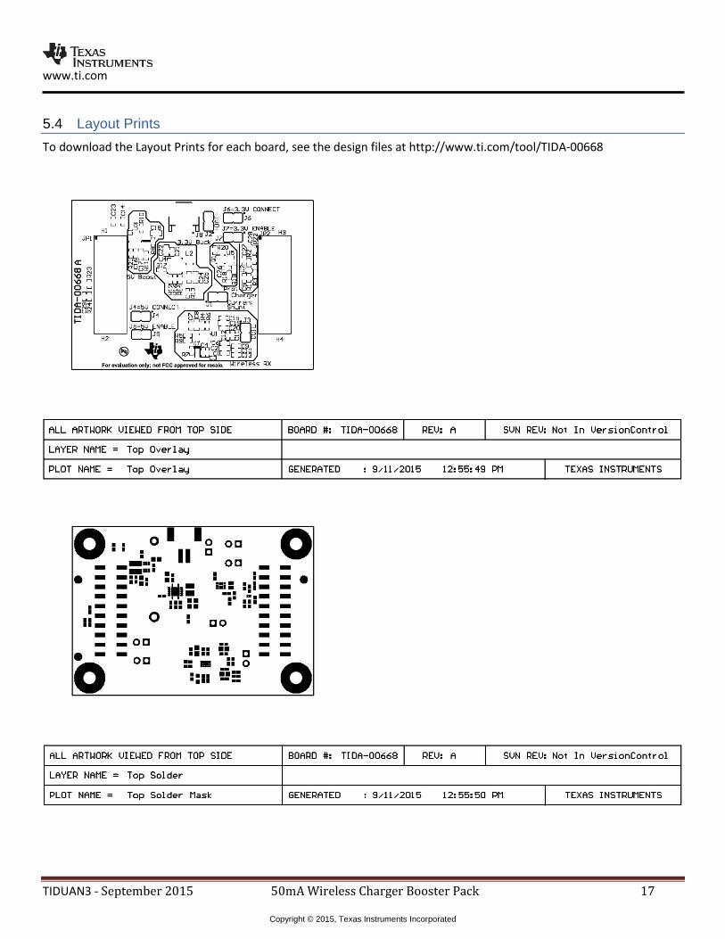
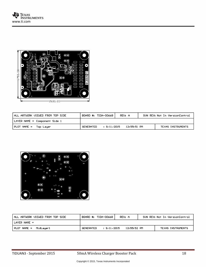
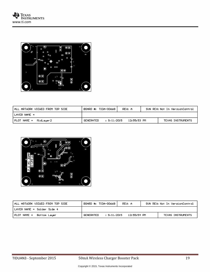
5.4 Layout Prints To download the Layout Prints for each board, see the design files at http://www.ti.com/tool/TIDA-00668
www.ti.com
TIDUAN3 - September 2015 50mA Wireless Charger Booster Pack 18
Copyright © 2015, Texas Instruments Incorporated
www.ti.com
TIDUAN3 - September 2015 50mA Wireless Charger Booster Pack 19
Copyright © 2015, Texas Instruments Incorporated
www.ti.com
TIDUAN3 - September 2015 50mA Wireless Charger Booster Pack 20
Copyright © 2015, Texas Instruments Incorporated
www.ti.com
TIDUAN3 - September 2015 50mA Wireless Charger Booster Pack 21
Copyright © 2015, Texas Instruments Incorporated
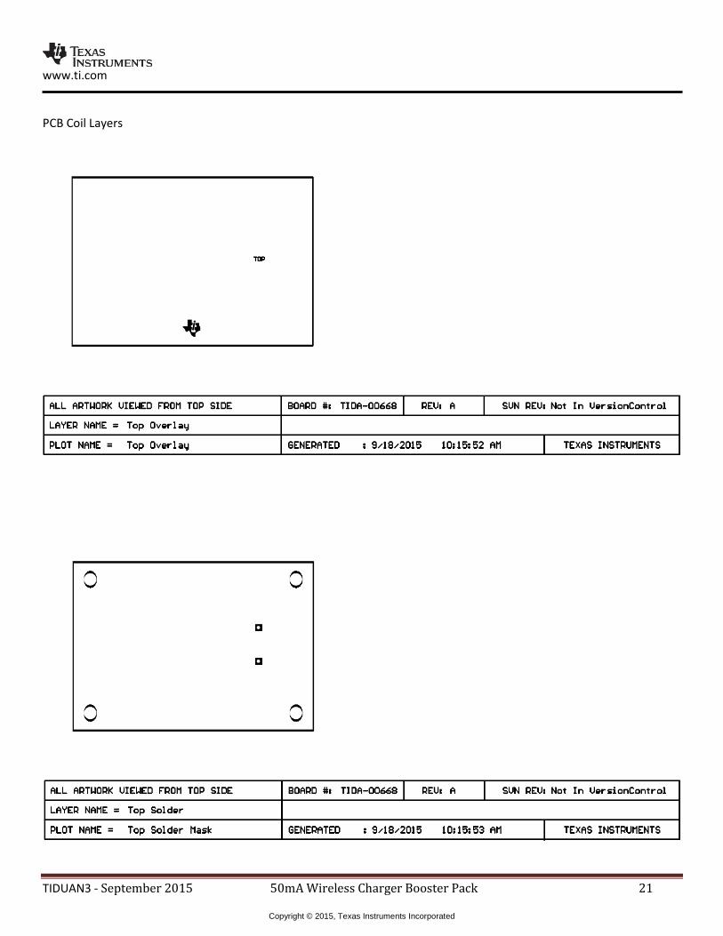
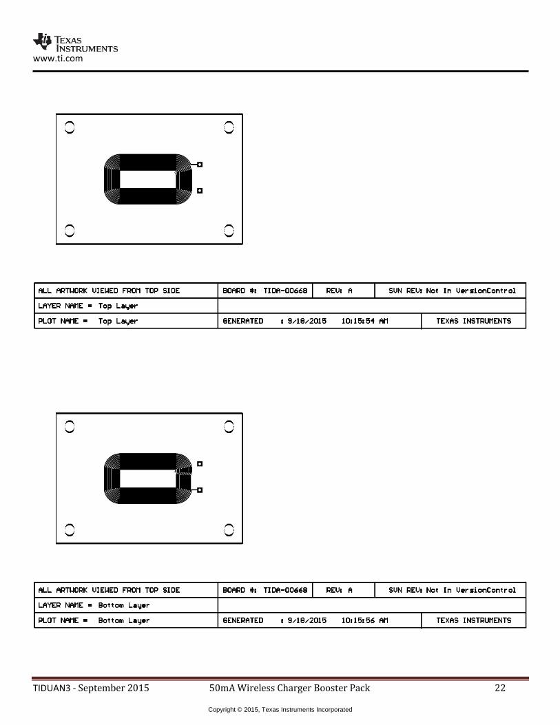
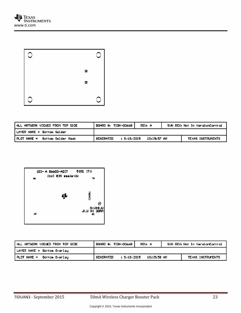
PCB Coil Layers
www.ti.com
TIDUAN3 - September 2015 50mA Wireless Charger Booster Pack 22
Copyright © 2015, Texas Instruments Incorporated
www.ti.com
TIDUAN3 - September 2015 50mA Wireless Charger Booster Pack 23
Copyright © 2015, Texas Instruments Incorporated
www.ti.com
TIDUAN3 - September 2015 50mA Wireless Charger Booster Pack 24
Copyright © 2015, Texas Instruments Incorporated
5.5 Booster Pack Pins The Booster Pack pin configuration is in the table below
Low Power Wireless Booster Pack 40Pin Pin J29 Pin Name Function IC Pin # Pin J29 Pin Name Function IC Pin #
Pin J30 Pin Name Function IC Pin # Pin J30 Pin Name Function IC Pin #
1 A1 3.3V_Main 2 C1 5V 1 D20 2 B20 GND 3 A2 Analog In
4 C2 GND
3 D19
4 B19 PWM/GPIO
5 A3 UART/RX
6 C3
5 D18
6 B18 SPI CS/GPIO
7 A4 UART/TX
8 C4
7 D17
8 B17 GPIO
9 A5 GPIO
10 C5
9 D16
10 B16 RESET RST 11 A6 Analog In Battery ADC 12 C6
11 D15
12 B15 SPI/MOSI
13 A7 SPI CLK
14 C7
13 D14
14 B14 SPI/MISO
15 A8 GPIO P3.4 VBAT_OK 16 C8
15 D13
16 B13 SPI/CS/DISPLAY
17 A9 I2C/SCL
18 C9
17 D12
18 B12 SPI/CS/Other
19 A10 I2C/SDA 20 C10 19 D11 20 B11 GPIO P1.3 VOUT_EN
5.6 Altium Project To download the Altium project files for each board, see the design files at http://www.ti.com/tool/TIDA-00668
IMPORTANT NOTICE FOR TI REFERENCE DESIGNS
Texas Instruments Incorporated ("TI") reference designs are solely intended to assist designers (“Buyers”) who are developing systems thatincorporate TI semiconductor products (also referred to herein as “components”). Buyer understands and agrees that Buyer remainsresponsible for using its independent analysis, evaluation and judgment in designing Buyer’s systems and products.TI reference designs have been created using standard laboratory conditions and engineering practices. TI has not conducted anytesting other than that specifically described in the published documentation for a particular reference design. TI may makecorrections, enhancements, improvements and other changes to its reference designs.Buyers are authorized to use TI reference designs with the TI component(s) identified in each particular reference design and to modify thereference design in the development of their end products. HOWEVER, NO OTHER LICENSE, EXPRESS OR IMPLIED, BY ESTOPPELOR OTHERWISE TO ANY OTHER TI INTELLECTUAL PROPERTY RIGHT, AND NO LICENSE TO ANY THIRD PARTY TECHNOLOGYOR INTELLECTUAL PROPERTY RIGHT, IS GRANTED HEREIN, including but not limited to any patent right, copyright, mask work right,or other intellectual property right relating to any combination, machine, or process in which TI components or services are used.Information published by TI regarding third-party products or services does not constitute a license to use such products or services, or awarranty or endorsement thereof. Use of such information may require a license from a third party under the patents or other intellectualproperty of the third party, or a license from TI under the patents or other intellectual property of TI.TI REFERENCE DESIGNS ARE PROVIDED "AS IS". TI MAKES NO WARRANTIES OR REPRESENTATIONS WITH REGARD TO THEREFERENCE DESIGNS OR USE OF THE REFERENCE DESIGNS, EXPRESS, IMPLIED OR STATUTORY, INCLUDING ACCURACY ORCOMPLETENESS. TI DISCLAIMS ANY WARRANTY OF TITLE AND ANY IMPLIED WARRANTIES OF MERCHANTABILITY, FITNESSFOR A PARTICULAR PURPOSE, QUIET ENJOYMENT, QUIET POSSESSION, AND NON-INFRINGEMENT OF ANY THIRD PARTYINTELLECTUAL PROPERTY RIGHTS WITH REGARD TO TI REFERENCE DESIGNS OR USE THEREOF. TI SHALL NOT BE LIABLEFOR AND SHALL NOT DEFEND OR INDEMNIFY BUYERS AGAINST ANY THIRD PARTY INFRINGEMENT CLAIM THAT RELATES TOOR IS BASED ON A COMBINATION OF COMPONENTS PROVIDED IN A TI REFERENCE DESIGN. IN NO EVENT SHALL TI BELIABLE FOR ANY ACTUAL, SPECIAL, INCIDENTAL, CONSEQUENTIAL OR INDIRECT DAMAGES, HOWEVER CAUSED, ON ANYTHEORY OF LIABILITY AND WHETHER OR NOT TI HAS BEEN ADVISED OF THE POSSIBILITY OF SUCH DAMAGES, ARISING INANY WAY OUT OF TI REFERENCE DESIGNS OR BUYER’S USE OF TI REFERENCE DESIGNS.TI reserves the right to make corrections, enhancements, improvements and other changes to its semiconductor products and services perJESD46, latest issue, and to discontinue any product or service per JESD48, latest issue. Buyers should obtain the latest relevantinformation before placing orders and should verify that such information is current and complete. All semiconductor products are soldsubject to TI’s terms and conditions of sale supplied at the time of order acknowledgment.TI warrants performance of its components to the specifications applicable at the time of sale, in accordance with the warranty in TI’s termsand conditions of sale of semiconductor products. Testing and other quality control techniques for TI components are used to the extent TIdeems necessary to support this warranty. Except where mandated by applicable law, testing of all parameters of each component is notnecessarily performed.TI assumes no liability for applications assistance or the design of Buyers’ products. Buyers are responsible for their products andapplications using TI components. To minimize the risks associated with Buyers’ products and applications, Buyers should provideadequate design and operating safeguards.Reproduction of significant portions of TI information in TI data books, data sheets or reference designs is permissible only if reproduction iswithout alteration and is accompanied by all associated warranties, conditions, limitations, and notices. TI is not responsible or liable forsuch altered documentation. Information of third parties may be subject to additional restrictions.Buyer acknowledges and agrees that it is solely responsible for compliance with all legal, regulatory and safety-related requirementsconcerning its products, and any use of TI components in its applications, notwithstanding any applications-related information or supportthat may be provided by TI. Buyer represents and agrees that it has all the necessary expertise to create and implement safeguards thatanticipate dangerous failures, monitor failures and their consequences, lessen the likelihood of dangerous failures and take appropriateremedial actions. Buyer will fully indemnify TI and its representatives against any damages arising out of the use of any TI components inBuyer’s safety-critical applications.In some cases, TI components may be promoted specifically to facilitate safety-related applications. With such components, TI’s goal is tohelp enable customers to design and create their own end-product solutions that meet applicable functional safety standards andrequirements. Nonetheless, such components are subject to these terms.No TI components are authorized for use in FDA Class III (or similar life-critical medical equipment) unless authorized officers of the partieshave executed an agreement specifically governing such use.Only those TI components that TI has specifically designated as military grade or “enhanced plastic” are designed and intended for use inmilitary/aerospace applications or environments. Buyer acknowledges and agrees that any military or aerospace use of TI components thathave not been so designated is solely at Buyer's risk, and Buyer is solely responsible for compliance with all legal and regulatoryrequirements in connection with such use.TI has specifically designated certain components as meeting ISO/TS16949 requirements, mainly for automotive use. In any case of use ofnon-designated products, TI will not be responsible for any failure to meet ISO/TS16949.IMPORTANT NOTICE
Mailing Address: Texas Instruments, Post Office Box 655303, Dallas, Texas 75265Copyright © 2015, Texas Instruments Incorporated