LT3010/LT3010-5 - 50mA, 3V to 80V Low Dropout Micropower ... · LT3010/LT3010-5 1 30105fe FEATURES...
18
LT3010/LT3010-5 1 30105fe FEATURES APPLICATIONS DESCRIPTION 50mA, 3V to 80V Low Dropout Micropower Linear Regulator The LT ® 3010 is a high voltage, micropower low dropout linear regulator. The device is capable of supplying 50mA output current with a dropout voltage of 300mV. Designed for use in battery-powered or high voltage systems, the low quiescent current (30µA operating and 1µA in shutdown) makes the LT3010 an ideal choice. Quiescent current is also well controlled in dropout. Other features of the LT3010 include the ability to operate with very small output capacitors. The regulators are stable with only 1µF on the output while most older devices re- quire between 10µF and 100µF for stability. Small ceramic capacitors can be used without the necessary addition of ESR as is common with other regulators. Internal protec- tion circuitry includes reverse-battery protection, current limiting, thermal limiting and reverse current protection. The device is available in a fixed output voltage of 5V and as an adjustable device with a 1.275V reference voltage. The LT3010 regulator is available in the 8-lead MSOP pack- age with an exposed pad for enhanced thermal handling capability. n Wide Input Voltage Range: 3V to 80V n Low Quiescent Current: 30µA n Low Dropout Voltage: 300mV n Output Current: 50mA n Thermally Enhanced 8-Lead MSOP Package n No Protection Diodes Needed n Fixed Output Voltage: 5V (LT3010-5) n Adjustable Output from 1.275V to 60V (LT3010) n 1µA Quiescent Current in Shutdown n Stable with 1µF Output Capacitor n Stable with Aluminum, Tantalum or Ceramic Capacitors n Reverse-Battery Protection n No Reverse Current Flow from Output n Thermal Limiting n Low Current High Voltage Regulators n Regulator for Battery-Powered Systems n Telecom Applications n Automotive Applications 5V Supply with Shutdown Dropout Voltage TYPICAL APPLICATION IN LT3010-5 SHDN 1μF V IN 5.4V TO 80V OUT SENSE GND 30105 TA01 V OUT 5V 50mA V SHDN (PIN 5) <0.3V >2.0V OUTPUT OFF ON 1μF OUTPUT CURRENT (mA) 0 250 300 350 40 30105 TA02 200 150 10 20 30 50 100 50 0 DROPOUT VOLTAGE (mV) L, LT, LTC, LTM, Linear Technology and the Linear logo are registered trademarks and ThinSOT is a trademark of Linear Technology Corporation. All other trademarks are the property of their respective owners.
Transcript of LT3010/LT3010-5 - 50mA, 3V to 80V Low Dropout Micropower ... · LT3010/LT3010-5 1 30105fe FEATURES...
LT3010/LT3010-5
130105fe
FEATURES
APPLICATIONS
DESCRIPTION
50mA, 3V to 80V Low Dropout
Micropower Linear Regulator
The LT®3010 is a high voltage, micropower low dropout linear regulator. The device is capable of supplying 50mA output current with a dropout voltage of 300mV. Designed for use in battery-powered or high voltage systems, the low quiescent current (30µA operating and 1µA in shutdown) makes the LT3010 an ideal choice. Quiescent current is also well controlled in dropout.
Other features of the LT3010 include the ability to operate with very small output capacitors. The regulators are stable with only 1µF on the output while most older devices re-quire between 10µF and 100µF for stability. Small ceramic capacitors can be used without the necessary addition of ESR as is common with other regulators. Internal protec-tion circuitry includes reverse-battery protection, current limiting, thermal limiting and reverse current protection.
The device is available in a fixed output voltage of 5V and as an adjustable device with a 1.275V reference voltage. The LT3010 regulator is available in the 8-lead MSOP pack-age with an exposed pad for enhanced thermal handling capability.
n Wide Input Voltage Range: 3V to 80Vn Low Quiescent Current: 30µAn Low Dropout Voltage: 300mVn Output Current: 50mAn Thermally Enhanced 8-Lead MSOP Packagen No Protection Diodes Neededn Fixed Output Voltage: 5V (LT3010-5)n Adjustable Output from 1.275V to 60V (LT3010)n 1µA Quiescent Current in Shutdownn Stable with 1µF Output Capacitorn Stable with Aluminum, Tantalum or Ceramic
Capacitorsn Reverse-Battery Protectionn No Reverse Current Flow from Outputn Thermal Limiting
n Low Current High Voltage Regulatorsn Regulator for Battery-Powered Systemsn Telecom Applicationsn Automotive Applications
5V Supply with Shutdown
Dropout Voltage
TYPICAL APPLICATION
IN
LT3010-5
SHDN1µF
VIN5.4V TO80V
OUT
SENSEGND
30105 TA01
VOUT5V50mA
VSHDN (PIN 5)<0.3V>2.0V
OUTPUTOFFON
1µF
OUTPUT CURRENT (mA)0
250
300
350
40
30105 TA02
200
150
10 20 30 50
100
50
0
DROP
OUT
VOLT
AGE
(mV)
L, LT, LTC, LTM, Linear Technology and the Linear logo are registered trademarks and ThinSOT is a trademark of Linear Technology Corporation. All other trademarks are the property of their respective owners.

LT3010/LT3010-5
230105fe
ABSOLUTE MAXIMUM RATINGS
IN Pin Voltage ........................................................ ±80VOUT Pin Voltage ..................................................... ±60VIN to OUT Differential Voltage ................................ ±80VADJ Pin Voltage ....................................................... ±7VSHDN Pin Input Voltage ......................................... ±80VOutput Short-Circuit Duration ......................... IndefiniteStorage Temperature Range .................. –65°C to 150°COperating Junction Temperature Range
(Notes 3, 10, 11) LT3010E ............................................. –40°C to 125°C LT3010H ............................................ –40°C to 140°C
LT3010MP.......................................... –55°C to 125°CLead Temperature (Soldering, 10 sec) ................. 300°C
(Note 1)
(LT3010E, LT3010MP) The l denotes the specifications which apply over the –40°C to 125°C (LT3010E) or –55°C to 125°C (LT3010MP) operating temperature range, otherwise specifications are at TA = 25°C.
PIN CONFIGURATION
1234
OUTSENSE/ADJ*
NCGND
8765
INNCNCSHDN
TOP VIEW
MS8E PACKAGE8-LEAD PLASTIC MSOP
9GND
*SENSE FOR LT3010-5, ADJ FOR LT3010
TJMAX = 125°C (LT3010E/LT3010MP), θJA = 40°C/W, θJC = 16°C/W†TJMAX = 140°C (LT3010H), θJA = 40°C/W, θJC = 16°C/W†
SEE APPLICATIONS INFORMATION SECTION. EXPOSED PAD (PIN 9) IS GND, MUST BE SOLDERED TO PCB
†MEASURED AT BOTTOM PAD
PARAMETER CONDITIONS MIN TYP MAX UNITS
Minimum Input Voltage LT3010 ILOAD = 50mA l 3 4 V
Regulated Output Voltage (Note 3)
LT3010-5 VIN = 5.5V, ILOAD = 1mA 6V < VIN < 80V, 1mA < ILOAD < 50mA
l
4.925 4.850
5.000 5.000
5.075 5.150
V V
ADJ Pin Voltage (Notes 2, 3) LT3010 VIN = 3V, ILOAD = 1mA 4V < VIN < 80V, 1mA < ILOAD < 50mA
l
1.258 1.237
1.275 1.275
1.292 1.313
V V
ORDER INFORMATIONLEAD FREE FINISH TAPE AND REEL PART MARKING* PACKAGE DESCRIPTION TEMPERATURE RANGE
LT3010EMS8E#PBF LT3010EMS8E#TRPBF LTZF 8-Lead Plastic MSOP –40°C to 125°C
LT3010EMS8E-5#PBF LT3010EMS8E-5#TRPBF LTAEF 8-Lead Plastic MSOP –40°C to 125°C
LT3010HMS8E#PBF LT3010HMS8E#TRPBF LTCLP 8-Lead Plastic MSOP –40°C to 140°C
LT3010HMS8E-5#PBF LT3010HMS8E-5#TRPBF LTCLQ 8-Lead Plastic MSOP –40°C to 140°C
LT3010MPMS8E#PBF LT3010MPMS8E#TRPBF LTZF 8-Lead Plastic MSOP –55°C to 125°C
LT3010MPMS8E-5#PBF LT3010MPMS8E-5#TRPBF LTAEF 8-Lead Plastic MSOP –55°C to 125°C
LEAD BASED FINISH TAPE AND REEL PART MARKING* PACKAGE DESCRIPTION TEMPERATURE RANGE
LT3010EMS8E LT3010EMS8E#TR LTZF 8-Lead Plastic MSOP –40°C to 125°C
LT3010EMS8E-5 LT3010EMS8E-5#TR LTAEF 8-Lead Plastic MSOP –40°C to 125°C
LT3010HMS8E LT3010HMS8E #TR LTCLP 8-Lead Plastic MSOP –40°C to 140°C
LT3010HMS8E-5 LT3010HMS8E-5 #TR LTCLQ 8-Lead Plastic MSOP –40°C to 140°C
LT3010MPMS8E LT3010MPMS8E#TR LTZF 8-Lead Plastic MSOP –55°C to 125°C
LT3010MPMS8E-5 LT3010MPMS8E-5#TR LTAEF 8-Lead Plastic MSOP –55°C to 125°C
Consult LTC Marketing for parts specified with wider operating temperature ranges. *The temperature grade is identified by a label on the shipping container.For more information on lead free part marking, go to: http://www.linear.com/leadfree/ For more information on tape and reel specifications, go to: http://www.linear.com/tapeandreel/
ELECTRICAL CHARACTERISTICS
LT3010/LT3010-5
330105fe
ELECTRICAL CHARACTERISTICS (LT3010E, LT3010MP) The l denotes the specifications which apply over the –40°C to 125°C (LT3010E) or –55°C to 125°C (LT3010MP) operating temperature range, otherwise specifications are at TA = 25°C.
PARAMETER CONDITIONS MIN TYP MAX UNITS
Line Regulation LT3010-5 ΔVIN = 5.5V to 80V, ILOAD = 1mA LT3010 (Note 2) ΔVIN = 3V to 80V, ILOAD = 1mA
l 3 3
15 13
mV mV
Load Regulation LT3010-5 VIN = 6V, ΔILOAD = 1mA to 50mA VIN = 6V, ΔILOAD = 1mA to 50mA
l
25 50 90
mV mV
LT3010 (Note 2) VIN = 4V, ΔILOAD = 1mA to 50mA VIN = 4V, ΔILOAD = 1mA to 50mA
l
10 20 32
mV mV
Dropout Voltage VIN = VOUT(NOMINAL) (Notes 4, 5)
ILOAD = 1mA ILOAD = 1mA
l
100 150 190
mV mV
ILOAD = 10mA ILOAD = 10mA
l
200 260 350
mV mV
ILOAD = 50mA ILOAD = 50mA
l
300 370 550
mV mV
GND Pin Current VIN = VOUT(NOMINAL) (Notes 4, 6)
ILOAD = 0mA ILOAD = 1mA ILOAD = 10mA ILOAD = 50mA
l
l
l
l
30 100 400 1.8
60 180 700 3.3
µA µA µA
mA
Output Voltage Noise COUT = 10µF, ILOAD = 50mA, BW = 10Hz to 100kHz 100 µVRMS
ADJ Pin Bias Current (Note 7) 50 100 nA
Shutdown Threshold VOUT = Off to On VOUT = On to Off
l
l
0.3
1.3 1.1
2 V V
SHDN Pin Current (Note 8)
VSHDN = 0V VSHDN = 6V
0.5 0.1
2 0.5
µA µA
Quiescent Current in Shutdown VIN = 6V, VSHDN = 0V 1 5 µA
Ripple Rejection LT3010 VIN = 7V(Avg), VRIPPLE = 0.5VP-P, fRIPPLE = 120Hz, ILOAD = 50mA LT3010-5 VIN = 7V(Avg), VRIPPLE = 0.5VP-P, fRIPPLE = 120Hz, ILOAD = 50mA
65 60
75 68
dB dB
Current Limit VIN = 7V, VOUT = 0V LT3010-5 VIN = 6V, ΔVOUT = –0.1V LT3010 (Note 2) VIN = 4V, ΔVOUT = –0.1V
l
l
60 60
140 mA mA mA
Input Reverse Leakage Current VIN = –80V, VOUT = 0V l 6 mA
Reverse Output Current (Note 9)
LT3010-5 VOUT = 5V, VIN < 5V LT3010 (Note 2) VOUT = 1.275V, VIN < 1.275V
10 8
20 15
µA µA
(LT3010H) The l denotes the specifications which apply over the –40°C to 140°C operating temperature range, otherwise specifications are at TA = 25°C.
PARAMETER CONDITIONS MIN TYP MAX UNITS
Minimum Input Voltage LT3010 ILOAD = 50mA l 3 4.25 V
Regulated Output Voltage (Note 3)
LT3010-5 VIN = 5.5V, ILOAD = 1mA 6V < VIN < 80V, 1mA < ILOAD < 50mA
l
4.925 4.825
5.000 5.000
5.075 5.15
V V
ADJ Pin Voltage (Notes 2, 3) LT3010 VIN = 3V, ILOAD = 1mA 4.25V < VIN < 80V, 1mA < ILOAD < 50mA
l
1.258 1.230
1.275 1.275
1.292 1.313
V V
Line Regulation LT3010-5 ΔVIN = 5.5V to 80V, ILOAD = 1mA LT3010 (Note 2) ΔVIN = 3V to 80V, ILOAD = 1mA
l
l
3 3
20 15
mV mV
Load Regulation LT3010-5 VIN = 6V, ΔILOAD = 1mA to 50mA VIN = 6V, ΔILOAD = 1mA to 50mA
l
25 50 100
mV mV
LT3010 (Note 2) VIN = 4V, ΔILOAD = 1mA to 50mA VIN = 4.25V, ΔILOAD = 1mA to 50mA
l
10 20 45
mV mV
LT3010/LT3010-5
430105fe
ELECTRICAL CHARACTERISTICS (LT3010H) The l denotes the specifications which apply over the –40°C to 140°C operating temperature range, otherwise specifications are at TA = 25°C.
PARAMETER CONDITIONS MIN TYP MAX UNITS
Dropout Voltage VIN = VOUT(NOMINAL) (Notes 4, 5)
ILOAD = 1mA ILOAD = 1mA
l
100 150 220
mV mV
ILOAD = 10mA ILOAD = 10mA
l
200 260 380
mV mV
ILOAD = 50mA ILOAD = 50mA
l
300 370 600
mV mV
GND Pin Current VIN = VOUT(NOMINAL) (Notes 4, 6)
ILOAD = 0mA ILOAD = 1mA ILOAD = 10mA ILOAD = 50mA
l
l
l
l
30 100 400 1.8
80 200 750 3.5
µA µA µA
mA
Output Voltage Noise COUT = 10µF, ILOAD = 250mA, BW = 10Hz to 100kHz 100 µVRMS
ADJ Pin Bias Current (Note 7) 50 100 nA
Shutdown Threshold VOUT = Off to On VOUT = On to Off
l
l
0.3
1.3 0.8
2 V V
SHDN Pin Current (Note 8)
VSHDN = 0V VSHDN = 6V
0.5 0.1
2 0.5
µA µA
Quiescent Current in Shutdown VIN = 6V, VSHDN = 0V 1 5 µA
Ripple Rejection LT3010 VIN = 7V(Avg), VRIPPLE = 0.5VP-P, fRIPPLE = 120Hz, ILOAD = 50mA LT3010-5 VIN = 7V(Avg), VRIPPLE = 0.5VP-P, fRIPPLE = 120Hz, ILOAD = 50mA
65 60
75 68
dB dB
Current Limit VIN = 7V, VOUT = 0V LT3010-5 VIN = 6V, ΔVOUT = –0.1V LT3010 (Note 2) VIN = 4.25V, ΔVOUT = –0.1V
l
l
l
55 55
140 mA mA mA
Input Reverse Leakage Current VIN = –80V, VOUT = 0V l 6 mA
Reverse Output Current (Note 9)
LT3010-5 VOUT = 5V, VIN < 5V LT3010 (Note 2) VOUT = 1.275V, VIN < 1.275V
10 8
20 15
µA µA
Note 1: Stresses beyond those listed under Absolute Maximum Ratings may cause permanent damage to the device. Exposure to any Absolute Maximum Rating condition for extended periods may affect device reliability and lifetime.Note 2: The LT3010 (adjustable version) is tested and specified for these conditions with the ADJ pin connected to the OUT pin.Note 3: Operating conditions are limited by maximum junction temperature. The regulated output voltage specification will not apply for all possible combinations of input voltage and output current. When operating at maximum input voltage, the output current range must be limited. When operating at maximum output current, the input voltage range must be limited.Note 4: To satisfy requirements for minimum input voltage, the LT3010 (adjustable version) is tested and specified for these conditions with an external resistor divider (249k bottom, 392k top) for an output voltage of 3.3V. The external resistor divider will add a 5µA DC load on the output.Note 5: Dropout voltage is the minimum input to output voltage differential needed to maintain regulation at a specified output current. In dropout, the output voltage will be equal to (VIN – VDROPOUT).Note 6: GND pin current is tested with VIN = VOUT (nominal) and a current source load. This means the device is tested while operating in its dropout region. This is the worst-case GND pin current. The GND pin current will decrease slightly at higher input voltages.
Note 7: ADJ pin bias current flows into the ADJ pin.Note 8: SHDN pin current flows out of the SHDN pin.Note 9: Reverse output current is tested with the IN pin grounded and the OUT pin forced to the rated output voltage. This current flows into the OUT pin and out the GND pin.Note 10: The LT3010E is guaranteed to meet performance specifications from 0°C to 125°C operating junction temperature. Specifications over the –40°C to 125°C operating junction temperature range are assured by design, characterization and correlation with statistical process controls. The LT3010H is tested to the LT3010H Electrical Characteristics table at 140°C operating junction temperature. The LT3010MP is 100% tested and guaranteed over the –55°C to 125°C operating junction temperature range. High junction temperatures degrade operating lifetimes. Operating lifetime is derated at junction temperatures greater than 125°C.Note 11: This IC includes overtemperature protection that is intended to protect the device during momentary overload conditions. Junction temperature will exceed 125°C (LT3010E and LT3010MP) or 140°C (LT3010H) when overtemperature protection is active. Continuous operation above the specified maximum operating junction temperature may impair device reliability.
LT3010/LT3010-5
530105fe
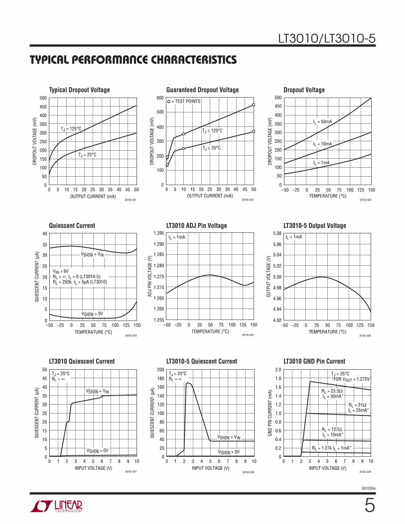
TYPICAL PERFORMANCE CHARACTERISTICS
Typical Dropout Voltage
Guaranteed Dropout Voltage
Dropout Voltage
Quiescent Current
LT3010 ADJ Pin Voltage
LT3010-5 Output Voltage
LT3010 Quiescent Current
LT3010-5 Quiescent Current
LT3010 GND Pin Current
OUTPUT CURRENT (mA)0
DROP
OUT
VOLT
AGE
(mV)
300
400
500
40
30105 G01
200
100
250
350
450
150
50
0105 2015 30 35 4525 50
TJ = 125°C
TJ = 25°C
OUTPUT CURRENT (mA)
0
DROP
OUT
VOLT
AGE
(mV)
200
400
600
100
300
500
10 20 30 40
30105 G02
5050 15 25 35 45
= TEST POINTS
TJ ≤ 125°C
TJ ≤ 25°C
TEMPERATURE (°C)
0
DROP
OUT
VOLT
AGE
(mV)
50
150
200
250
500
350
30105 G03
100
400
450
300
–50 0 50 75–25 25 100 150125
IL = 50mA
IL = 10mA
IL = 1mA
TEMPERATURE (°C)–50
QUIE
SCEN
T CU
RREN
T (µ
A)
35
25
30105 G04
20
10
–25 0 50
5
0
40
30
25
15
75 100 125 150
VSHDN = VIN
VSHDN = 0V
VIN > 6VRL = ∞, IL = 0 (LT3010-5)RL = 250k, IL = 5µA (LT3010)
TEMPERATURE (°C)
ADJ
PIN
VOLT
AGE
(V)
1.290
30105 G05
1.275
1.265
1.260
1.255
1.295
1.285
1.280
1.270
–50 0 50 75–25 25 100 150125
IL = 1mA
TEMPERATURE (°C)
OUTP
UT V
OLTA
GE (V
)
5.06
30105 G06
5.00
4.96
4.94
4.92
5.08
5.04
5.02
4.98
–50 0 50 75–25 25 100 150125
IL = 1mA
INPUT VOLTAGE (V)0
QUIE
SCEN
T CU
RREN
T (µ
A)
30
40
50
8
30105 G07
20
10
25
35
45
15
5
021 43 6 7 95 10
TJ = 25°CRL = ∞
VSHDN = VIN
VSHDN = 0V
INPUT VOLTAGE (V)0
QUIE
SCEN
T CU
RREN
T (µ
A)
120
160
200
8
30105 G08
80
40
100
140
180
60
20
021 43 6 7 95 10
TJ = 25°CRL = ∞
VSHDN = VIN
VSHDN = 0V
INPUT VOLTAGE (V)0
GND
PIN
CURR
ENT
(mA)
1.2
1.6
2.0
8
30105 G09
0.8
0.4
1.0
1.4
1.8
0.6
0.2
021 43 6 7 95 10
TJ = 25°C*FOR VOUT = 1.275V
RL = 25.5Ω IL = 50mA*
RL = 51Ω IL = 25mA*
RL = 127Ω IL = 10mA*
RL = 1.27k IL = 1mA*
LT3010/LT3010-5
630105fe
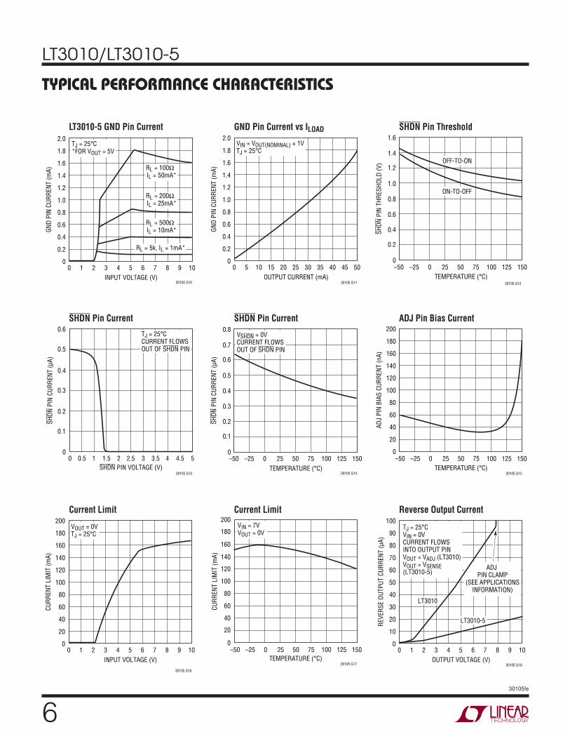
TYPICAL PERFORMANCE CHARACTERISTICS
LT3010-5 GND Pin Current
GND Pin Current vs ILOAD
SHDN Pin Threshold
SHDN Pin Current
SHDN Pin Current
ADJ Pin Bias Current
Current Limit
Current Limit
Reverse Output Current
INPUT VOLTAGE (V)0
GND
PIN
CURR
ENT
(mA)
1.2
1.6
2.0
8
30105 G10
0.8
0.4
1.0
1.4
1.8
0.6
0.2
021 43 6 7 95 10
TJ = 25°C*FOR VOUT = 5V
RL = 100Ω IL = 50mA*
RL = 200Ω IL = 25mA*
RL = 500Ω IL = 10mA*
RL = 5k, IL = 1mA*
OUTPUT CURRENT (mA)0
GND
PIN
CURR
ENT
(mA)
1.2
1.6
2.0
40
30105 G11
0.8
0.4
1.0
1.4
1.8
0.6
0.2
0105 2015 30 35 4525 50
VIN = VOUT(NOMINAL) + 1VTJ = 25°C
–50 25–25 0 50 75 100 125 150TEMPERATURE (°C)
SHDN
PIN
THR
ESHO
LD (V
)
1.4
30105 G12
0.8
0.4
0.2
0
1.6
1.2
1.0
0.6
OFF-TO-ON
ON-TO-OFF
SHDN PIN VOLTAGE (V)
0
SHDN
PIN
CUR
RENT
(µA)
0.2
0.4
0.6
0.1
0.3
0.5
1 2 3 4
30105 G13
50.50 1.5 2.5 3.5 4.5
TJ = 25°CCURRENT FLOWSOUT OF SHDN PIN
–50 25–25 0 50 75 100 125 150TEMPERATURE (°C)
SHDN
PIN
CUR
RENT
(µA)
0.7
30105 G14
0.4
0.2
0.1
0
0.8
0.6
0.5
0.3
VSHDN = 0VCURRENT FLOWSOUT OF SHDN PIN
TEMPERATURE (°C)
ADJ
PIN
BIAS
CUR
RENT
(nA)
180
30105 G15
80
40
20
0
200
140
160
120
100
60
–50 0 50 75–25 25 100 150125
INPUT VOLTAGE (V)0
CURR
ENT
LIM
IT (m
A)
120
160
200
8
30105 G16
80
40
100
140
180
60
20
021 43 6 7 95 10
VOUT = 0VTJ = 25°C
TEMPERATURE (°C)
0
CURR
ENT
LIM
IT (m
A)
20
60
80
100
200
140
30105 G17
40
160
180
120
–50 0 50 75–25 25 100 150125
VIN = 7VVOUT = 0V
OUTPUT VOLTAGE (V)0
REVE
RSE
OUTP
UT C
URRE
NT (µ
A)
60
80
100
8
30105 G18
40
20
50
70
90
30
10
021 43 6 7 95 10
LT3010
LT3010-5
TJ = 25°CVIN = 0VCURRENT FLOWSINTO OUTPUT PINVOUT = VADJ (LT3010)VOUT = VSENSE(LT3010-5)
ADJ PIN CLAMP
(SEE APPLICATIONSINFORMATION)

LT3010/LT3010-5
730105fe
Reverse Output Current
Input Ripple Rejection
Input Ripple Rejection
LT3010 Minimum Input Voltage
Load Regulation
Output Noise Spectral Density
LT3010-5 10Hz to 100kHz Output Noise
LT3010-5 Transient Response
TYPICAL PERFORMANCE CHARACTERISTICS
70
40
20
10
0
80
60
50
30
–50 0 50 75–25 25 100 150125TEMPERATURE (°C)
REVE
RSE
OUTP
UT C
URRE
NT (µ
A)
3010 G19
LT3010-5
LT3010
VIN = 0VVOUT = VADJ = 1.275V (LT3010)VOUT = VSENSE = 5V (LT3010-5)
TEMPERATURE (°C)
60
RIPP
LE R
EJEC
TION
(dB)
62
66
68
70
80
74
30105 G20
64
76
78
72
–50 0 50 75–25 25 100 150125
VIN = 7V + 0.5VP-P RIPPLE AT f = 120HzIL = 50mAVOUT = 1.275V
FREQUENCY (Hz)10
40
RIPP
LE R
EJEC
TION
(dB)
50
60
70
80
100 1k 10k 100k 1M
30105 G21
30
20
10
0
90
100VIN = 7V + 50mVRMS RIPPLEIL = 50mA
COUT = 10µF
COUT = 1µF
TEMPERATURE (°C)
MIN
IMUM
INPU
T VO
LTAG
E (V
)
3.5
30105 G22
2.0
1.0
0.5
0
4.0
3.0
2.5
1.5
–50 0 50 75–25 25 100 150125
ILOAD = 50mA
–50 0 50 75–25 25 100 150125TEMPERATURE (°C)
LOAD
REG
ULAT
ION
(mV)
–5
30105 G23
–20
–30
–40
–50
–35
–45
0
–10
–15
–25
ΔIL = 1mA TO 50mA
LT3010
LT3010-5
FREQUENCY (Hz)
0.1
OUTP
UT N
OISE
SPE
CTRA
L DE
NSIT
Y (µ
V/√H
z)1
10 1k 10k 100k
30105 G24
0.01100
10COUT = 1µFIL = 50mA
VOUT100µV/DIV
1ms/DIV30105 G25
COUT = 1µFIL = 50mA
TIME (µs)0
OUTP
UT V
OLTA
GEDE
VIAT
ION
(V)
LOAD
CUR
RENT
(mA)
–0.1
0.1
800
30105 G26
25
–0.2
0
0.2
50
0
200 400 600 1000
VIN = 6VCIN = 1µF CERAMICCOUT = 1µF CERAMICΔILOAD = 1mA TO 50mA
LT3010/LT3010-5
830105fe
PIN FUNCTIONSOUT (Pin 1): Output. The output supplies power to the load. A minimum output capacitor of 1µF is required to prevent oscillations. Larger output capacitors will be required for applications with large transient loads to limit peak volt-age transients. See the Applications Information section for more information on output capacitance and reverse output characteristics.
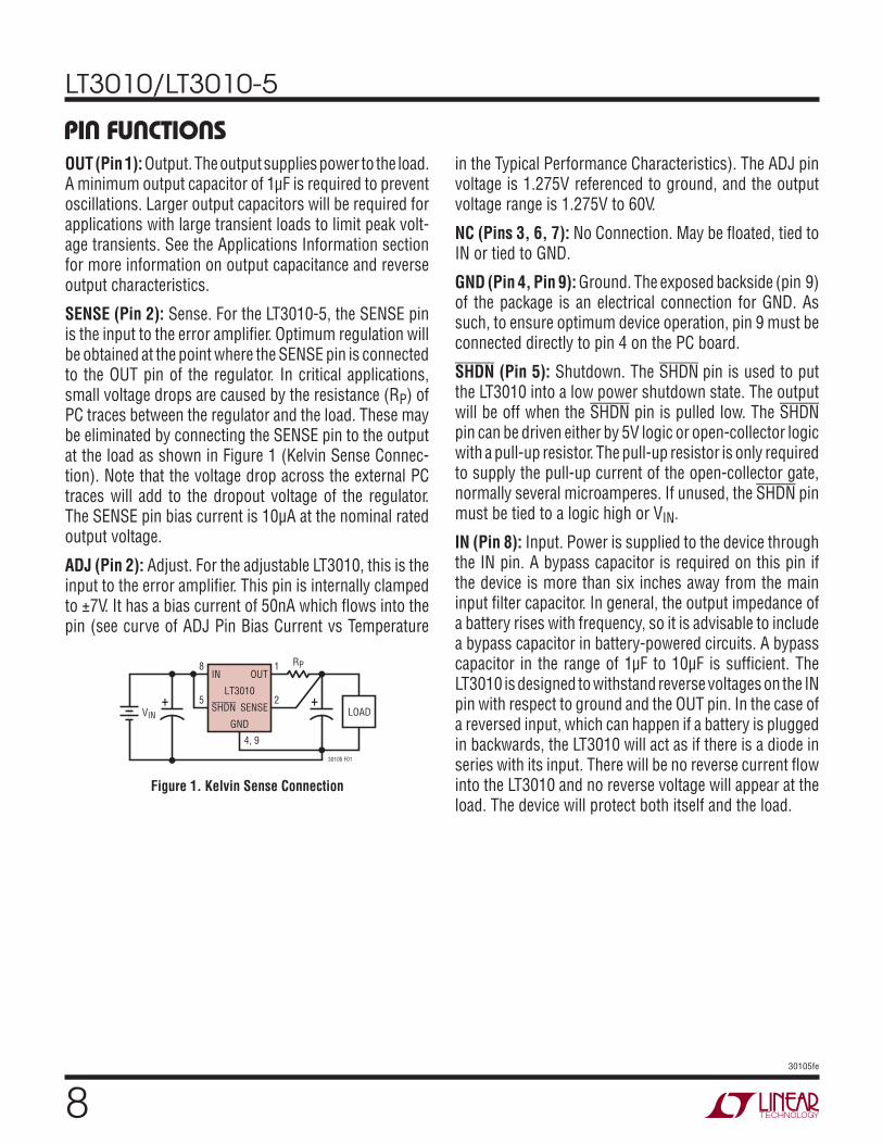
SENSE (Pin 2): Sense. For the LT3010-5, the SENSE pin is the input to the error amplifier. Optimum regulation will be obtained at the point where the SENSE pin is connected to the OUT pin of the regulator. In critical applications, small voltage drops are caused by the resistance (RP) of PC traces between the regulator and the load. These may be eliminated by connecting the SENSE pin to the output at the load as shown in Figure 1 (Kelvin Sense Connec-tion). Note that the voltage drop across the external PC traces will add to the dropout voltage of the regulator. The SENSE pin bias current is 10µA at the nominal rated output voltage.
ADJ (Pin 2): Adjust. For the adjustable LT3010, this is the input to the error amplifier. This pin is internally clamped to ±7V. It has a bias current of 50nA which flows into the pin (see curve of ADJ Pin Bias Current vs Temperature
in the Typical Performance Characteristics). The ADJ pin voltage is 1.275V referenced to ground, and the output voltage range is 1.275V to 60V.
NC (Pins 3, 6, 7): No Connection. May be floated, tied to IN or tied to GND.
GND (Pin 4, Pin 9): Ground. The exposed backside (pin 9) of the package is an electrical connection for GND. As such, to ensure optimum device operation, pin 9 must be connected directly to pin 4 on the PC board.
SHDN (Pin 5): Shutdown. The SHDN pin is used to put the LT3010 into a low power shutdown state. The output will be off when the SHDN pin is pulled low. The SHDN pin can be driven either by 5V logic or open-collector logic with a pull-up resistor. The pull-up resistor is only required to supply the pull-up current of the open-collector gate, normally several microamperes. If unused, the SHDN pin must be tied to a logic high or VIN.
IN (Pin 8): Input. Power is supplied to the device through the IN pin. A bypass capacitor is required on this pin if the device is more than six inches away from the main input filter capacitor. In general, the output impedance of a battery rises with frequency, so it is advisable to include a bypass capacitor in battery-powered circuits. A bypass capacitor in the range of 1µF to 10µF is sufficient. The LT3010 is designed to withstand reverse voltages on the IN pin with respect to ground and the OUT pin. In the case of a reversed input, which can happen if a battery is plugged in backwards, the LT3010 will act as if there is a diode in series with its input. There will be no reverse current flow into the LT3010 and no reverse voltage will appear at the load. The device will protect both itself and the load.
Figure 1. Kelvin Sense Connection
IN
SHDN
LT3010
VIN
OUT
SENSE
GND
1 RP
2
8
5
4, 9
30105 F01
+ +LOAD

LT3010/LT3010-5
930105fe
APPLICATIONS INFORMATIONThe LT3010 is a 50mA high voltage low dropout regulator with micropower quiescent current and shutdown. The device is capable of supplying 50mA at a dropout voltage of 300mV. The low operating quiescent current (30µA) drops to 1µA in shutdown. In addition to the low quies-cent current, the LT3010 incorporates several protection features which make it ideal for use in battery-powered systems. The device is protected against both reverse input and reverse output voltages. In battery backup ap-plications where the output can be held up by a backup battery when the input is pulled to ground, the LT3010 acts like it has a diode in series with its output and prevents reverse current flow.
Adjustable Operation
The adjustable version of the LT3010 has an output voltage range of 1.275V to 60V. The output voltage is set by the ratio of two external resistors as shown in Figure 2. The device servos the output to maintain the voltage at the adjust pin at 1.275V referenced to ground. The current in R1 is then equal to 1.275V/R1 and the current in R2 is the current in R1 plus the ADJ pin bias current. The ADJ pin bias current, 50nA at 25°C, flows through R2 into the ADJ pin. The output voltage can be calculated using the formula in Figure 2. The value of R1 should be less than 250k to minimize errors in the output voltage caused by the ADJ pin bias current. Note that in shutdown the output is turned off and the divider current will be zero.
A small capacitor (C1) placed in parallel with the top resistor (R2) of the output divider is necessary for stability and tran-sient performance of the adjustable LT3010. The impedance of C1 at 10kHz should be less than the value of R1.
Figure 2. Adjustable Operation
The adjustable device is tested and specified with the ADJ pin tied to the OUT pin and a 5µA DC load (unless otherwise specified) for an output voltage of 1.275V. Speci-fications for output voltages greater than 1.275V will be proportional to the ratio of the desired output voltage to 1.275V; (VOUT/1.275V). For example, load regulation for an output current change of 1mA to 50mA is –10mV typical at VOUT = 1.275V. At VOUT = 12V, load regulation is:
(12V/1.275V)•(–10mV)=–94mV
Output Capacitance and Transient Response
The LT3010 is designed to be stable with a wide range of output capacitors. The ESR of the output capacitor affects stability, most notably with small capacitors. A minimum output capacitor of 1µF with an ESR of 3Ω or less is recommended to prevent oscillations. The LT3010 is a micropower device and output transient response will be a function of output capacitance. Larger values of output capacitance decrease the peak deviations and provide improved transient response for larger load current changes. Bypass capacitors, used to decouple individual components powered by the LT3010, will increase the effective output capacitor value.
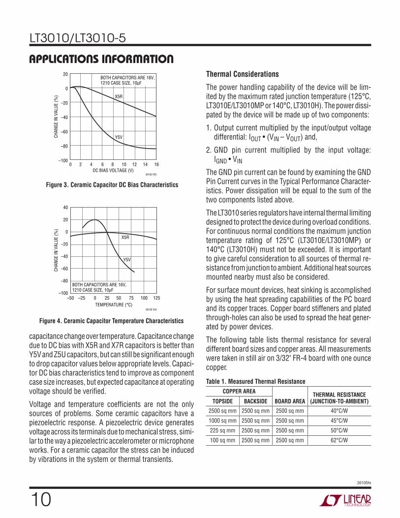
Extra consideration must be given to the use of ceramic capacitors. Ceramic capacitors are manufactured with a variety of dielectrics, each with different behavior across temperature and applied voltage. The most common dielectrics used are specified with EIA temperature char-acteristic codes of Z5U, Y5V, X5R and X7R. The Z5U and Y5V dielectrics are good for providing high capacitances in a small package, but they tend to have strong voltage and temperature coefficients as shown in Figures 3 and 4. When used with a 5V regulator, a 16V 10µF Y5V capacitor can exhibit an effective value as low as 1µF to 2µF for the DC bias voltage applied and over the operating tempera-ture range. The X5R and X7R dielectrics result in more stable characteristics and are more suitable for use as the output capacitor. The X7R type has better stability across temperature, while the X5R is less expensive and is avail-able in higher values. Care still must be exercised when using X5R and X7R capacitors; the X5R and X7R codes only specify operating temperature range and maximum
IN
LT3010VIN
OUT
ADJ
GND30105 F02
VOUT
R2 C1
R1
+
R2R1
VOUT = 1.275V
VADJ = 1.275VIADJ = 50nA AT 25°COUTPUT RANGE = 1.275V TO 60V
+ (IADJ)(R2)1 + ( )
LT3010/LT3010-5
1030105fe
APPLICATIONS INFORMATION
capacitance change over temperature. Capacitance change due to DC bias with X5R and X7R capacitors is better than Y5V and Z5U capacitors, but can still be significant enough to drop capacitor values below appropriate levels. Capaci-tor DC bias characteristics tend to improve as component case size increases, but expected capacitance at operating voltage should be verified.
Voltage and temperature coefficients are not the only sources of problems. Some ceramic capacitors have a piezoelectric response. A piezoelectric device generates voltage across its terminals due to mechanical stress, simi-lar to the way a piezoelectric accelerometer or microphone works. For a ceramic capacitor the stress can be induced by vibrations in the system or thermal transients.
Thermal Considerations
The power handling capability of the device will be lim-ited by the maximum rated junction temperature (125°C, LT3010E/LT3010MP or 140°C, LT3010H). The power dissi-pated by the device will be made up of two components:
1. Output current multiplied by the input/output voltage differential: IOUT •(VIN – VOUT) and,
2. GND pin current multiplied by the input voltage: IGND •VIN
The GND pin current can be found by examining the GND Pin Current curves in the Typical Performance Character-istics. Power dissipation will be equal to the sum of the two components listed above.
The LT3010 series regulators have internal thermal limiting designed to protect the device during overload conditions. For continuous normal conditions the maximum junction temperature rating of 125°C (LT3010E/LT3010MP) or 140°C (LT3010H) must not be exceeded. It is important to give careful consideration to all sources of thermal re-sistance from junction to ambient. Additional heat sources mounted nearby must also be considered.
For surface mount devices, heat sinking is accomplished by using the heat spreading capabilities of the PC board and its copper traces. Copper board stiffeners and plated through-holes can also be used to spread the heat gener-ated by power devices.
The following table lists thermal resistance for several different board sizes and copper areas. All measurements were taken in still air on 3/32" FR-4 board with one ounce copper.
Table 1. Measured Thermal ResistanceCOPPER AREA
BOARD AREATHERMAL RESISTANCE
(JUNCTION-TO-AMBIENT)TOPSIDE BACKSIDE
2500 sq mm 2500 sq mm 2500 sq mm 40°C/W
1000 sq mm 2500 sq mm 2500 sq mm 45°C/W
225 sq mm 2500 sq mm 2500 sq mm 50°C/W
100 sq mm 2500 sq mm 2500 sq mm 62°C/W
Figure 3. Ceramic Capacitor DC Bias Characteristics
Figure 4. Ceramic Capacitor Temperature Characteristics
DC BIAS VOLTAGE (V)
CHAN
GE IN
VAL
UE (%
)
30105 F03
20
0
–20
–40
–60
–80
–1000 4 8 102 6 12 14
X5R
Y5V
16
BOTH CAPACITORS ARE 16V,1210 CASE SIZE, 10µF
TEMPERATURE (°C)–50
40
20
0
–20
–40
–60
–80
–10025 75
30105 F04
–25 0 50 100 125
Y5V
CHAN
GE IN
VAL
UE (%
)
X5R
BOTH CAPACITORS ARE 16V,1210 CASE SIZE, 10µF
LT3010/LT3010-5
1130105fe
APPLICATIONS INFORMATIONThe thermal resistance junction-to-case (θJC), measured at the exposed pad on the back of the die, is 16°C/W.
Continuous operation at large input/output voltage dif-ferentials and maximum load current is not practical due to thermal limitations. Transient operation at high input/output differentials is possible. The approximate thermal time constant for a 2500sq mm 3/32" FR-4 board with maximum topside and backside area for one ounce copper is 3 seconds. This time constant will increase as more thermal mass is added (i.e. vias, larger board, and other components).
For an application with transient high power peaks, average power dissipation can be used for junction temperature calculations as long as the pulse period is significantly less than the thermal time constant of the device and board.
Calculating Junction Temperature
Example 1: Given an output voltage of 5V, an input volt-age range of 24V to 30V, an output current range of 0mA to 50mA, and a maximum ambient temperature of 50°C, what will the maximum junction temperature be?
The power dissipated by the device will be equal to:
IOUT(MAX)•(VIN(MAX) – VOUT) + (IGND•VIN(MAX))
where:
IOUT(MAX) = 50mA
VIN(MAX) = 30V
IGND at (IOUT = 50mA, VIN = 30V) = 1mA
So:
P=50mA•(30V–5V)+(1mA•30V)=1.28W
The thermal resistance will be in the range of 40°C/W to 62°C/W depending on the copper area. So the junction temperature rise above ambient will be approximately equal to:
1.31W•50°C/W=65.5°C
The maximum junction temperature will then be equal to the maximum junction temperature rise above ambient plus the maximum ambient temperature or:
TJMAX = 50°C + 65.5°C = 115.5°C
Example 2: Given an output voltage of 5V, an input voltage of 48V that rises to 72V for 5ms(max) out of every 100ms, and a 5mA load that steps to 50mA for 50ms out of every 250ms, what is the junction temperature rise above ambi-ent? Using a 500ms period (well under the time constant of the board), power dissipation is as follows:
P1(48Vin,5mAload)=5mA•(48V–5V) +(200µA•48V)=0.23W
P2(48Vin,50mAload)=50mA•(48V–5V) +(1mA•48V)=2.20W
P3(72Vin,5mAload)=5mA•(72V–5V) +(200µA•72V)=0.35W
P4(72Vin,50mAload)=50mA•(72V–5V) +(1mA•72V)=3.42W
Operation at the different power levels is as follows:
76% operation at P1, 19% for P2, 4% for P3, and 1% for P4.
PEFF = 76%(0.23W) + 19%(2.20W) + 4%(0.35W) + 1%(3.42W) = 0.64W
With a thermal resistance in the range of 40°C/W to 62°C/W, this translates to a junction temperature rise above ambient of 26°C to 38°C.
High Temperature Operation
Care must be taken when designing LT3010H applications to operate at high ambient temperatures. The LT3010H works at elevated temperatures but erratic operation can occur due to unforeseen variations in external components. Some tantalum capacitors are available for high temperature operation, but ESR is often several ohms; capacitor ESR
LT3010/LT3010-5
1230105fe
APPLICATIONS INFORMATIONabove 3Ω is unsuitable for use with the LT3010H. Ceramic capacitor manufacturers (Murata, AVX, TDK, and Vishay Vitramon at this writing) now offer ceramic capacitors that are rated to 150°C using an X8R dielectric. Device instability will occur if output capacitor value and ESR are outside design limits at elevated temperature and operating DC voltage bias (see information on capacitor characteristics under Output Capacitance and Transient Response). Check each passive component for absolute value and voltage ratings over the operating temperature range.
Leakages in capacitors or from solder flux left after in-sufficient board cleaning adversely affects low quiescent current operation. Consider junction temperature increase due to power dissipation in both the junction and nearby components to ensure maximum specifications are not violated for the LT3010H or external components.
Protection Features
The LT3010 incorporates several protection features which make it ideal for use in battery-powered circuits. In ad-dition to the normal protection features associated with monolithic regulators, such as current limiting and thermal limiting, the device is protected against reverse-input volt-ages, and reverse voltages from output to input.
Current limit protection and thermal overload protection are intended to protect the device against current overload conditions at the output of the device. For normal opera-tion, the junction temperature should not exceed 125°C (LT3010E/LT3010MP) or 140°C (LT3010H).
The input of the device will withstand reverse voltages of 80V. Current flow into the device will be limited to less than 6mA (typically less than 100µA) and no negative voltage will appear at the output. The device will protect both itself and the load. This provides protection against batteries which can be plugged in backward.
The ADJ pin of the adjustable device can be pulled above or below ground by as much as 7V without damaging the device. If the input is left open circuit or grounded, the ADJ pin will act like an open circuit when pulled below ground, and like a large resistor (typically 100k) in series with a diode when pulled above ground. If the input is powered by a voltage source, pulling the ADJ pin below the reference voltage will cause the device to try and force the current limit current out of the output. This will cause the output to go to a unregulated high voltage. Pulling the ADJ pin above the reference voltage will turn off all output current.
In situations where the ADJ pin is connected to a resistor divider that would pull the ADJ pin above its 7V clamp volt-age if the output is pulled high, the ADJ pin input current must be limited to less than 5mA. For example, a resistor divider is used to provide a regulated 1.5V output from the 1.22V reference when the output is forced to 60V. The top resistor of the resistor divider must be chosen to limit the current into the ADJ pin to less than 5mA when the ADJ pin is at 7V. The 53V difference between the OUT and ADJ pins divided by the 5mA maximum current into the ADJ pin yields a minimum top resistor value of 10.6k.
LT3010/LT3010-5
1330105fe
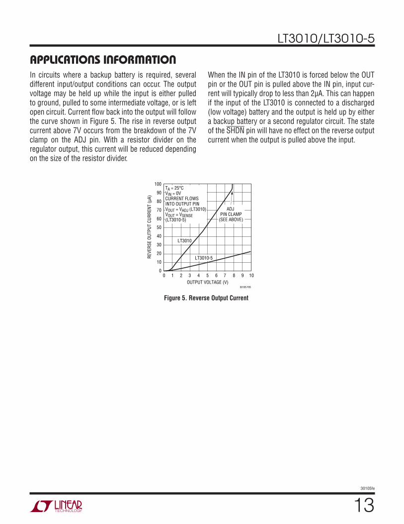
Figure 5. Reverse Output Current
OUTPUT VOLTAGE (V)
100
90
80
70
60
50
40
30
20
10
0
REVE
RSE
OUTP
UT C
URRE
NT (µ
A)
30105 F05
0 1 2 3 4 5 6 7 8 9 10
TA = 25°CVIN = 0VCURRENT FLOWS INTO OUTPUT PINVOUT = VADJ (LT3010)VOUT = VSENSE(LT3010-5)
LT3010
LT3010-5
ADJ PIN CLAMP
(SEE ABOVE)
APPLICATIONS INFORMATIONIn circuits where a backup battery is required, several different input/output conditions can occur. The output voltage may be held up while the input is either pulled to ground, pulled to some intermediate voltage, or is left open circuit. Current flow back into the output will follow the curve shown in Figure 5. The rise in reverse output current above 7V occurs from the breakdown of the 7V clamp on the ADJ pin. With a resistor divider on the regulator output, this current will be reduced depending on the size of the resistor divider.
When the IN pin of the LT3010 is forced below the OUT pin or the OUT pin is pulled above the IN pin, input cur-rent will typically drop to less than 2µA. This can happen if the input of the LT3010 is connected to a discharged (low voltage) battery and the output is held up by either a backup battery or a second regulator circuit. The state of the SHDN pin will have no effect on the reverse output current when the output is pulled above the input.
LT3010/LT3010-5
1430105fe
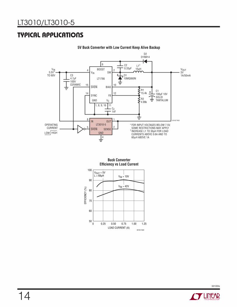
5V Buck Converter with Low Current Keep Alive Backup
Buck Converter Efficiency vs Load Current
TYPICAL APPLICATIONS
BOOSTVIN
6
2
10
12
D110MQ060N
R115.4k
VOUT5V1A/50mA
4
4
8
5
1
2
15
14
11CC1nF
FOR INPUT VOLTAGES BELOW 7.5V, SOME RESTRICTIONS MAY APPLYINCREASE L1 TO 30µH FOR LOADCURRENTS ABOVE 0.6A AND TO 60μH ABOVE 1A
1, 8, 9, 16
LT1766
SHDN
SYNC
SW
BIAS
FB
VCGND
C20.33µF
C1100µF 10VSOLIDTANTALUM
L1†
15µH
D2D1N914
R24.99k
30105 TA03
C34.7µF 100VCERAMIC
VIN 5.5V*TO 60V
+
SENSE
OUTIN
SHDN
LT3010-5
GND
OPERATINGCURRENT
HIGHLOW
*
†
LOAD CURRENT (A)0
EFFI
CIEN
CY (%
)
80
90
100
1.00
30105 TA04
70
60
500.25 0.50 0.75 1.25
VIN = 10V
VIN = 42V
VOUT = 5VL = 68µH
LT3010/LT3010-5
1530105fe
TYPICAL APPLICATIONS
Constant Brightness for Indicator LED over Wide Input Voltage Range
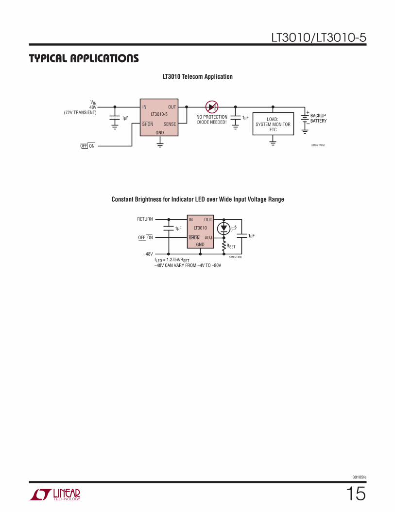
LT3010 Telecom Application
IN
LT3010
SHDN
1µF
RETURN
OFF ON
–48V
OUT
ADJGND
30105 TA06
1µF
RSET
ILED = 1.275V/RSET–48V CAN VARY FROM –4V TO –80V
+
–SENSE
OUTIN
SHDN
LT3010-5
GND
ONOFF
1µF 1µF
VIN48V
(72V TRANSIENT)LOAD:
SYSTEM MONITORETC
NO PROTECTIONDIODE NEEDED!
30105 TA05b
BACKUPBATTERY
LT3010/LT3010-5
1630105fe
MSOP (MS8E) 0910 REV I
0.53 ± 0.152(.021 ± .006)
SEATINGPLANE
NOTE:1. DIMENSIONS IN MILLIMETER/(INCH)2. DRAWING NOT TO SCALE3. DIMENSION DOES NOT INCLUDE MOLD FLASH, PROTRUSIONS OR GATE BURRS. MOLD FLASH, PROTRUSIONS OR GATE BURRS SHALL NOT EXCEED 0.152mm (.006") PER SIDE4. DIMENSION DOES NOT INCLUDE INTERLEAD FLASH OR PROTRUSIONS. INTERLEAD FLASH OR PROTRUSIONS SHALL NOT EXCEED 0.152mm (.006") PER SIDE5. LEAD COPLANARITY (BOTTOM OF LEADS AFTER FORMING) SHALL BE 0.102mm (.004") MAX6. EXPOSED PAD DIMENSION DOES NOT INCLUDE MOLD FLASH. MOLD FLASH ON E-PAD SHALL NOT EXCEED 0.254mm (.010") PER SIDE.
0.18(.007)
0.254(.010)
1.10(.043)MAX
0.22 – 0.38(.009 – .015)
TYP
0.86(.034)REF
0.65(.0256)
BSC
0° – 6° TYP
DETAIL “A”
DETAIL “A”
GAUGE PLANE
1 2 3 4
4.90 ± 0.152(.193 ± .006)
8
8
1
BOTTOM VIEW OFEXPOSED PAD OPTION
7 6 5
3.00 ± 0.102(.118 ± .004)
(NOTE 3)
3.00 ± 0.102(.118 ± .004)
(NOTE 4)
0.52(.0205)
REF
1.68(.066)
1.88(.074)
5.23(.206)MIN
3.20 – 3.45(.126 – .136)
1.68 ± 0.102(.066 ± .004)
1.88 ± 0.102(.074 ± .004) 0.889 ± 0.127
(.035 ± .005)
RECOMMENDED SOLDER PAD LAYOUT
0.65(.0256)
BSC0.42 ± 0.038
(.0165 ± .0015)TYP
0.1016 ± 0.0508(.004 ± .002)
DETAIL “B”
DETAIL “B”CORNER TAIL IS PART OF
THE LEADFRAME FEATURE.FOR REFERENCE ONLY
NO MEASUREMENT PURPOSE
0.05 REF
0.29REF
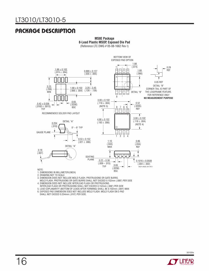
PACKAGE DESCRIPTIONMS8E Package
8-Lead Plastic MSOP, Exposed Die Pad(Reference LTC DWG # 05-08-1662 Rev I)
LT3010/LT3010-5
1730105fe
Information furnished by Linear Technology Corporation is believed to be accurate and reliable. However, no responsibility is assumed for its use. Linear Technology Corporation makes no representa-tion that the interconnection of its circuits as described herein will not infringe on existing patent rights.
REVISION HISTORYREV DATE DESCRIPTION PAGE NUMBER
D 5/10 Added MP-Grade to All SectionsUpdated Related Parts List
2 to 4, 10, 1218
E 4/11 Update MSOP Package Drawing 16
(Revision history begins at Rev D)
LT3010/LT3010-5
1830105fe
Linear Technology Corporation1630 McCarthy Blvd., Milpitas, CA 95035-7417 (408) 432-1900 l FAX: (408) 434-0507 l www.linear.com LINEAR TECHNOLOGY CORPORATION 2003
LT 0411 REV E • PRINTED IN USA
RELATED PARTSPART NUMBER DESCRIPTION COMMENTS
LT1676 60V, 440mA (IOUT), 100kHz, High Efficiency Step-Down DC/DC Converter
VIN: 7.4V to 60V, VOUT = 1.24V, IQ = 3.2mA, ISD = 2.5µA, S8 Package
LT1761 100mA, Low Noise Micropower, LDO VIN: 1.8V to 20V, VOUT = 1.22V, VDO = 0.3V, IQ = 20µA, ISD = <1µA, Low Noise < 20µVRMS, Stable with 1µF Ceramic Capacitors, ThinSOT™ Package
LT1762 150mA, Low Noise Micropower, LDO VIN: 1.8V to 20V, VOUT = 1.22V, VDO = 0.3V, IQ = 25µA, ISD = <1µA, Low Noise < 20µVRMS, MS8 Package
LT1763 500mA, Low Noise Micropower, LDO VIN: 1.8V to 20V, VOUT = 1.22V, VDO = 0.3V, IQ = 30µA, ISD = <1µA, Low Noise < 20µVRMS, S8 Package
LT1766 60V, 1.2A (IOUT), 200kHz, High Efficiency Step-Down DC/DC Converter
VIN: 5.5V to 60V, VOUT = 1.20V, IQ = 2.5mA, ISD = 25µA, TSSOP16/E Package
LT1776 40V, 550mA (IOUT), 200kHz, High Efficiency Step-Down DC/DC Converter
VIN: 7.4V to 40V, VOUT = 1.24V, IQ = 3.2mA, ISD = 30µA, N8, S8 Packages
LT1956 60V, 1.2A (IOUT), 500kHz, High Efficiency Step-Down DC/DC Converter
VIN: 5.5V to 60V, VOUT = 1.20V, IQ = 2.5mA, ISD = 25µA, TSSOP16/E Package
LT1962 300mA, Low Noise Micropower, LDO VIN: 1.8V to 20V, VOUT = 1.22V, VDO = 0.27V, IQ = 30µA, ISD = <1µA, Low Noise < 20µVRMS, MS8 Package
LT3011 50mA, High Voltage, Micropower LDO with PWRGD
VIN: 3V to 80V, VOUT: 1.275V to 60V, VDO = 0.3V, IQ = 46µA, ISD < 1µA, Low Noise: <100µVRMS PowerGood, Stable with 1µF Output Capacitor, 3mm × 3mm DFN-10 and Exposed MS12E Packages
LT3012 250mA, 4V to 80V, Low Dropout Micropower Linear Regulator
VIN: 4V to 80V, VOUT: 1.24V to 60V, VDO = 0.4V, IQ = 40µA, ISD < 1µA, TSSOP-16E and 4mm × 3mm DFN-12 Packages
LT3013 250mA, 4V to 80V, Low Dropout Micropower Linear Regulator with PWRGD
VIN: 4V to 80V, VOUT: 1.24V to 60V, VDO = 0.4V, IQ = 65µA, ISD < 1µA, PowerGood; TSSOP-16E and 4mm × 3mm DFN-12 Packages
LT3014 20mA, 3V to 80V, Low Dropout Micropower Linear Regulator
VIN: 3V to 80V (100V for 2ms, "HV" Version), VOUT: 1.22V to 60V, VDO = 0.35V, IQ = 7µA, ISD < 1µA, ThinSOT and 3mm × 3mm DFN-8 Packages
LT3050 100mA, Low Noise Linear Regulator with Precision Current and Diagnostic Functions
Input Voltage Range: 2V to 45V, Quiescent Current: 50μA, Dropout Voltage: 300mV; Low Noise: 30μVRMS (10Hz to 100kHz), Adjustable Output: VREF = 600mV; Programmable Precision Current Limit: ±5%, Programmable Minimum IOUT Monitor, Diagnostic IOUT Telemetry: 1/100th of IOUT, Fault Indicator: Current Limit, Minimum IOUT or Thermal Limit; Shutdown Current: < 1μA, Reverse Battery Protection, Current Limit Protection, Thermal Limit Protection, 12-Lead 3mm × 2mm DFN and MSOP Packages
LT3060 45V VIN, Micropower, Low Noise, 100mA Low Dropout Linear Regulator
Input Voltage Range: 1.7V to 45V, Quiescent Current: 40μA, Dropout Voltage: 300mV; Low Noise: 30μVRMS (10Hz to 100kHz), Adjustable Output: VREF = 600mV; Output Tolerance: ±2% Over Load, Line and Temperature, Single Capacitor Soft-Starts Reference and Lowers Output Noise, Shutdown Current: < 1μA, Reverse Battery Protection, Current Limit Foldback Protection, Thermal Limit Protection, 8-Lead 2mm × 2mm DFN and 8-Lead ThinSOT Packages
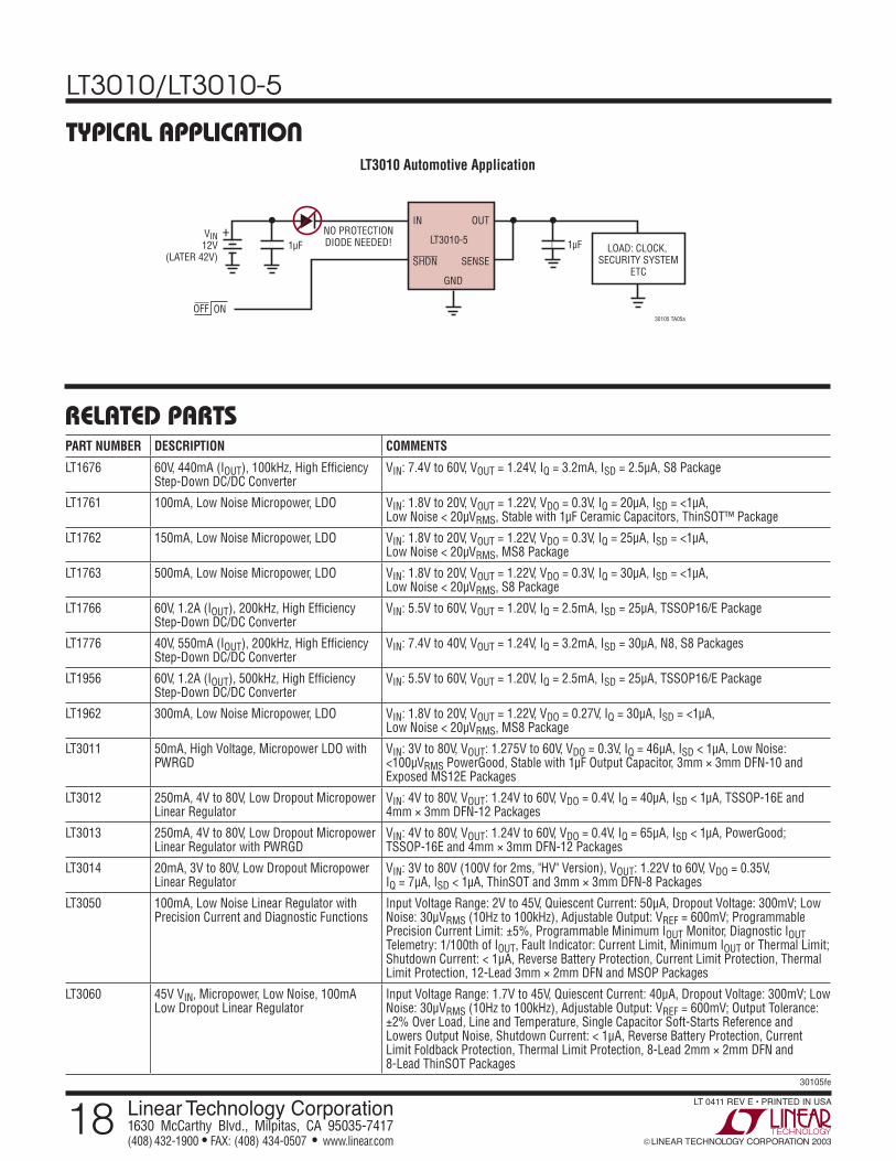
TYPICAL APPLICATIONLT3010 Automotive Application
+
SENSE
OUTIN
SHDN
LT3010-5
GND
ONOFF
1µF 1µFVIN12V
(LATER 42V)LOAD: CLOCK,
SECURITY SYSTEMETC
NO PROTECTIONDIODE NEEDED!
30105 TA05a