
4.2 Current Voltage Characteristics - KU ITTCjstiles/312/handouts/section 4_2 Current Voltage... ·...
29
10/19/2004 4_2 Current Voltage Characteristics empty.doc 1/2 Jim Stiles The Univ. of Kansas Dept. of EECS 4.2 Current Voltage Characteristics Reading Assignment: pp. 248-262 A. MOSFET Circuit Symbols HO: The Circuit Symbols of Enhancement MOSFETs B. i D Dependence on v DS and v GS Q: A: HO: A Mathematical Description of MOSFET Behavior
Transcript of 4.2 Current Voltage Characteristics - KU ITTCjstiles/312/handouts/section 4_2 Current Voltage... ·...

10/19/2004 4_2 Current Voltage Characteristics empty.doc 1/2
Jim Stiles The Univ. of Kansas Dept. of EECS
4.2 Current Voltage Characteristics Reading Assignment: pp. 248-262 A. MOSFET Circuit Symbols HO: The Circuit Symbols of Enhancement MOSFETs B. iD Dependence on vDS and vGS Q: A: HO: A Mathematical Description of MOSFET Behavior

10/19/2004 4_2 Current Voltage Characteristics empty.doc 2/2
Jim Stiles The Univ. of Kansas Dept. of EECS
Q: A: HO: Channel Resistance for Small vDS
C. Drain Output Resistance Q: A: HO: Drain Output Resistance
D. The Body Effect Q: A: HO: The Body Effect
10/19/2004 The Circuit Symbols of Enhancement MOSFETs.doc 1/1
Jim Stiles The Univ. of Kansas Dept. of EECS
The Circuit Symbols of Enhancement MOSFETs
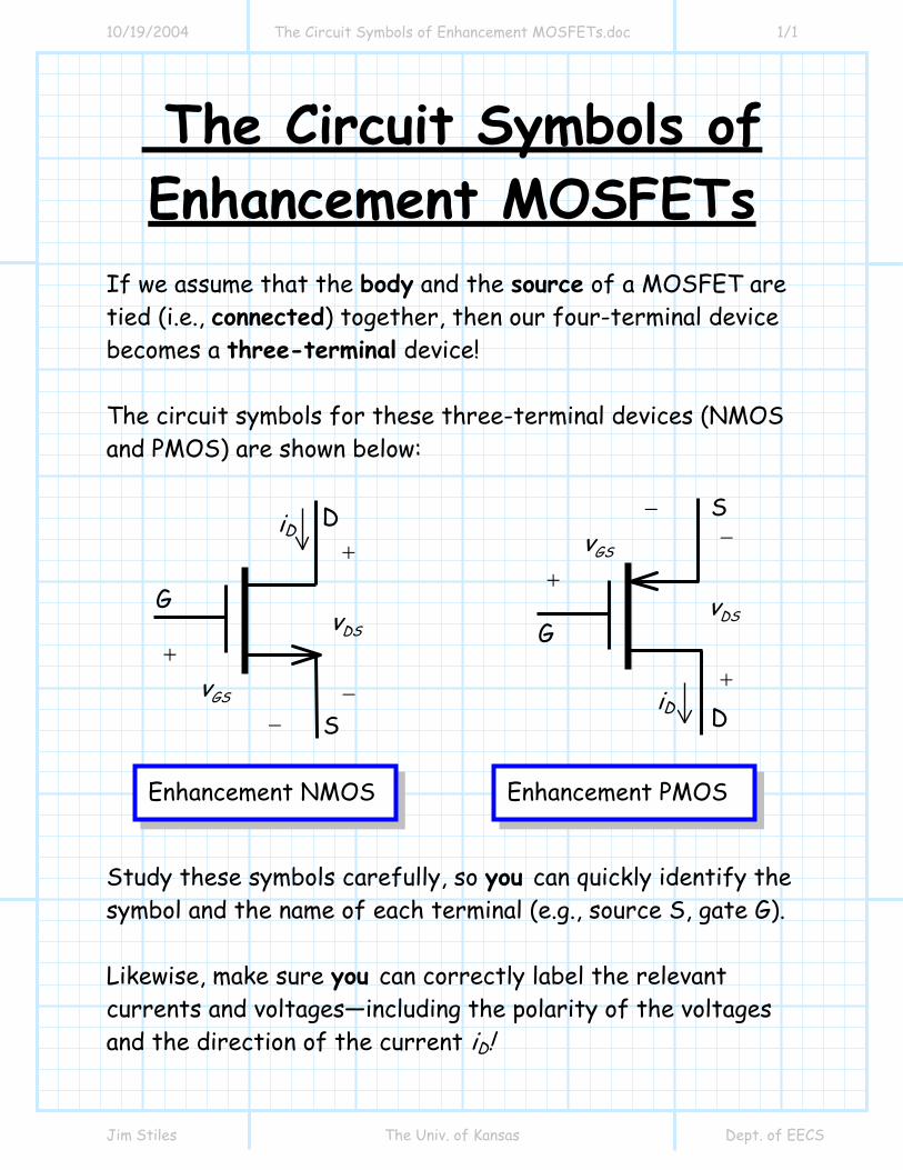
If we assume that the body and the source of a MOSFET are tied (i.e., connected) together, then our four-terminal device becomes a three-terminal device! The circuit symbols for these three-terminal devices (NMOS and PMOS) are shown below: Study these symbols carefully, so you can quickly identify the symbol and the name of each terminal (e.g., source S, gate G). Likewise, make sure you can correctly label the relevant currents and voltages—including the polarity of the voltages and the direction of the current iD!
DSv
+
−
GSv+
−
iD
G
S
D
DSv
−
+
GSv
−
+
G
D
S
iD
Enhancement NMOS Enhancement PMOS

10/19/2004 A Mathematical Description of MOSFET Behavior.doc 1/8
Jim Stiles The Univ. of Kansas Dept. of EECS
A Mathematical Description of
MOSFET Behavior A: A mathematical description of enhancement MOSFET behavior is relatively straightforward ! We actually need to concern ourselves with just 3 equations. Specifically, we express the drain current iD in terms of vGS and vDS for each of the three MOSFET modes (i.e., Cutoff, Triode, Saturation). Additionally, we need to mathematically define the boundaries between each of these three modes!
Q: We’ve learned an awful lot about enhancement MOSFETs, but we still have yet to established a mathematical relationships between iD, vGS, or vDS. How can we determine the correct numeric values for MOSFET voltages and currents?

10/19/2004 A Mathematical Description of MOSFET Behavior.doc 2/8
Jim Stiles The Univ. of Kansas Dept. of EECS
But first, we need to examine some fundamental physical parameters that describe a MOSFET device. These parameters include:
2 Process Transconductance Parameter A/Vk ′ ⎡ ⎤⎣ ⎦
Channel Aspect RatioWL
=
The Process Transconductance Parameter k ′ is a constant that depends on the process technology used to fabricate an integrated circuit. Therefore, all the transistors on a given substrate will typically have the same value of this parameter.
The Channel Aspect Ratio W L is simply the ratio of channel width W to channel length L. This is the MOSFET device parameter that can be altered and modified by the circuit designer to satisfy the requirements of the given circuit or transistor. We can likewise combine these parameter to form a single MOSFET device parameter K :
212
W AK k VL⎛ ⎞ ⎡ ⎤′= ⎜ ⎟ ⎢ ⎥⎣ ⎦⎝ ⎠
Now we can mathematically describe the behavior of an enhancement MOSFET! Well do this one mode at a time.

10/19/2004 A Mathematical Description of MOSFET Behavior.doc 3/8
Jim Stiles The Univ. of Kansas Dept. of EECS
CUTOFF This relationship is very simple—if the MOSFET is in cutoff, the drain current is simply zero !
0 (CUTOFF mode)Di =
TRIODE When in triode mode, the drain current is dependent on both vGS and vDS:
( )
( )
2
2
1 (TRIODE mode)2
2
GS tD DS DS
GS t DS DS
Wi k v V v vL
K v V v v
⎛ ⎞ ⎡ ⎤′= − −⎜ ⎟ ⎢ ⎥⎝ ⎠ ⎣ ⎦⎡ ⎤= − −⎣ ⎦
This equation is valid for both NMOS and PMOS transistors (if in TRIODE mode). Recall that for PMOS devices, the values of vGS and vDS are negative, but note that this will result (correctly so) in a positive value of iD.
SATURATION When in saturation mode, the drain current is (approximately) dependent on vGS only:

10/19/2004 A Mathematical Description of MOSFET Behavior.doc 4/8
Jim Stiles The Univ. of Kansas Dept. of EECS
( )
( )
2
2
1 (SATURATION mode)2
GS tD
GS t
Wi k v VL
K v V
⎛ ⎞′= −⎜ ⎟⎝ ⎠
= −
Thus, we see that the drain current in saturation is proportional to excess gate voltage squared! This equation is likewise valid for both NMOS and PMOS transistors (if in SATURATION mode).
A: We must determine the mathematical boundaries of each mode. Just as before, we will do this one mode at a time! CUTOFF A MOSFET is in cutoff when no channel has been induced. Thus, for an enhancement NMOS device:
if 0 then NMOS in CUTOFFGS tv V− <
Q: OK, so know we know the expression for drain current iD in each of the threeMOSFET modes, but how will we know what mode the MOSFET is in?

10/19/2004 A Mathematical Description of MOSFET Behavior.doc 5/8
Jim Stiles The Univ. of Kansas Dept. of EECS
Like wise, for an enhancement PMOS device:
if 0 then PMOS in CUTOFFGS tv V− >
TRIODE For triode mode, we know that a channel is induced (i.e., an inversion layer is present). Additionally, we know that when in triode mode, the voltage vDS is not sufficiently large for NMOS, or sufficiently small (i.e., sufficiently negative) for PMOS, to pinch off this induced channel. A: The answer to that question is surprisingly simple. The induced channel of an NMOS device is pinched off if the voltage vDS is greater than the excess gate voltage! I.E.:
if then NMOS channel is "pinched off"GS tDSv v V> −
Q: But how large does vDS need to be to pinch off an NMOS channel? How can we determine if pinch off has occurred?

10/19/2004 A Mathematical Description of MOSFET Behavior.doc 6/8
Jim Stiles The Univ. of Kansas Dept. of EECS
Conversely, for PMOS devices, we find that:
if then PMOS channel is "pinched off"GS tDSv v V< −
These statements of course mean that an NMOS channel is not pinched off if GS tDSv v V< − , and a PMOS channel is not pinched off if GS tDSv v V> − . Thus, we can say that an NMOS device is in the TRIODE mode:
if 0 and then NMOS in TRIODEGS t GS tDSv V v v V− > < −
Similarly, for PMOS:
if 0 and then PMOS in TRIODEGS t GS tDSv V v v V− < > −
SATURATION Recall for SATURATION mode that a channel is induced, and that channel is pinched off.

10/19/2004 A Mathematical Description of MOSFET Behavior.doc 7/8
Jim Stiles The Univ. of Kansas Dept. of EECS
Thus, we can state that for NMOS:
if 0 and then NMOS in SAT.GS t GS tDSv V v v V− > > − And for PMOS:
if 0 and then PMOS in SAT.GS t GS tDSv V v v V− < < − We now can construct a complete (continuous) expression relating drain current iD to voltages vDS and vGS. For an NMOS device, this expression is:
( )
( )
2DS
2DS
0 if 0
2 if 0 and v
if 0 and v
GS t
GS t GS t GS tD DS DS
GS t GS t GS t
v V
i K v V v v v V v V
K v V v V v V
⎧ − <⎪⎪⎪ ⎡ ⎤= − − − > < −⎨ ⎣ ⎦⎪⎪⎪ − − > > −⎩

10/19/2004 A Mathematical Description of MOSFET Behavior.doc 8/8
Jim Stiles The Univ. of Kansas Dept. of EECS
Likewise, for a PMOS device we find:
( )
( )
2DS
2DS
0 if 0
2 if 0 and v
if 0 and v
GS t
GS t GS t GS tD DS DS
GS t GS t GS t
v V
i K v V v v v V v V
K v V v V v V
⎧ − >⎪⎪⎪ ⎡ ⎤= − − − < > −⎨ ⎣ ⎦⎪⎪⎪ − − < < −⎩
Let’s take a look at what these expressions look like when we plot them. Specifically, for an NMOS device let’s plot iD versus vDS for different values of vGS:

10/19/2004 Channel Resistance for Small VDS.doc 1/10
Jim Stiles The Univ. of Kansas Dept. of EECS
Channel Resistance for Small VDS
Recall voltage vDS will be directly proportional to iD, provided that:
1. A conducting channel has been induced.
2. The value of vDS is small. Note for this situation, the MOSFET will be in triode region. Recall also that as we increase the value of vDS, the conducting channel will begin to pinch off—the current will no longer be directly proportional to vDS . Specifically, we have previously determined that there are two phenomena at work as we increase vDS while in the triode region:
1. Increasing vDS will increase the potential difference across the conducting channel, an effect that works to proportionally increase the drain current iD
2. Increasing vDS will decrease the conductivity of the induced channel, an effect that works to decrease the drain current iD.
10/19/2004 Channel Resistance for Small VDS.doc 2/10
Jim Stiles The Univ. of Kansas Dept. of EECS
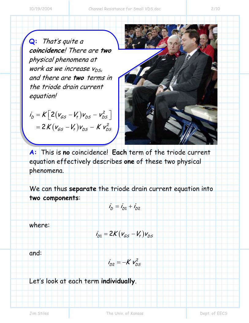
A: This is no coincidence! Each term of the triode current equation effectively describes one of these two physical phenomena. We can thus separate the triode drain current equation into two components:
1 2D D Di i i= + where:
( )1 2 GS tD DSi K v V v= − and:
22D DSi K v= −
Let’s look at each term individually.
Q: That’s quite a coincidence! There are two physical phenomena at work as we increase vDS, and there are two terms in the triode drain current equation!
( )( )
2
2
2
2GS tD DS DS
GS t DS DS
i K v V v vK v V v K v
⎡ ⎤= − −⎣ ⎦= − −

10/19/2004 Channel Resistance for Small VDS.doc 3/10
Jim Stiles The Univ. of Kansas Dept. of EECS
( )1 2 GS tD DSi K v V v= −
We first note that this term is directly proportional to vDS—if vDS increases 10%, the value of this term will increase 10%. Note that this is true regardless of the magnitude of vDS! Plotting this term, we get: It is evident that this term describes the first of our phenomenon:
1. Increasing vDS will increase the potential difference across the conducting channel, an effect that works to proportionally increase the drain current iD.
In other words, this first term would accurately describe the relationship between iD and vDS if the MOSFET induced channel behaved like a resistor! But of course, it does not behave like a resistor! The second term iD2 describes this very nonresistor-like behavior.
vDS
iD1
GS tv V−
( )1 2 GS tD DSi K v V v= −

10/19/2004 Channel Resistance for Small VDS.doc 4/10
Jim Stiles The Univ. of Kansas Dept. of EECS
2
2D DSi K v= −
A: This second term iD2 essentially describes the result of the second phenomena:
2. Increasing vDS will decrease the conductivity of the induced channel, an effect that works to decrease the drain current iD.
Q: My Gosh! It is apparent that iD2 is not directly proportional to vDS, but instead proportional to vDS squared!! Moreover, the minus sign out front means that as vDS increases, iD2 will actually decrease! This behavior is nothing like a resistor—what the heck is going on here??

10/19/2004 Channel Resistance for Small VDS.doc 5/10
Jim Stiles The Univ. of Kansas Dept. of EECS
Plotting this term, we get: A very unresistor-like behavior ! Now let’s add the two terms iD1 and iD2 together to get the total triode drain current iD :
vDS
iD2 GS tv V−
22D DSi K v= −
( )1 2 GS tD DSi K v V v= −
vDS
i
GS tv V−
22D DSi K v= −
( ) 22 GS tD DS DSi K v V v v⎡ ⎤= − −⎣ ⎦

10/19/2004 Channel Resistance for Small VDS.doc 6/10
Jim Stiles The Univ. of Kansas Dept. of EECS
It is apparent that the second term iD2 works to reduce the total drain current from its “resistor-like” value iD1. This of course is physically due to the reduction in channel conductivity as vDS increases. A: Absolutely true! Recall this is consistent with our earlier discussion about the induced channel—the channel conductivity begins to significantly degrade only when vDS becomes sufficiently large! Thus, we can conclude:
( )
( )
1
DS
2
for small v
D D
GS t DS
GS t DS
i iK v V v
Wk v V vL
≈
= −
⎛ ⎞′= −⎜ ⎟⎝ ⎠
Moreover, we can (for small vDS) approximate the induced channel as a resistor rDS of value DS DS DSr v i= :
Q: But look! It appears to me that for small values of vDS, the term iD2 is very small, and thus
1D Di i≈ (when vDS is small)!
10/19/2004 Channel Resistance for Small VDS.doc 7/10
Jim Stiles The Univ. of Kansas Dept. of EECS
( )
( ) DS
21 for small v
2
DSDS
D
DS
GS t DS
GS t
vri
vK v V v
K v V
=−
=−
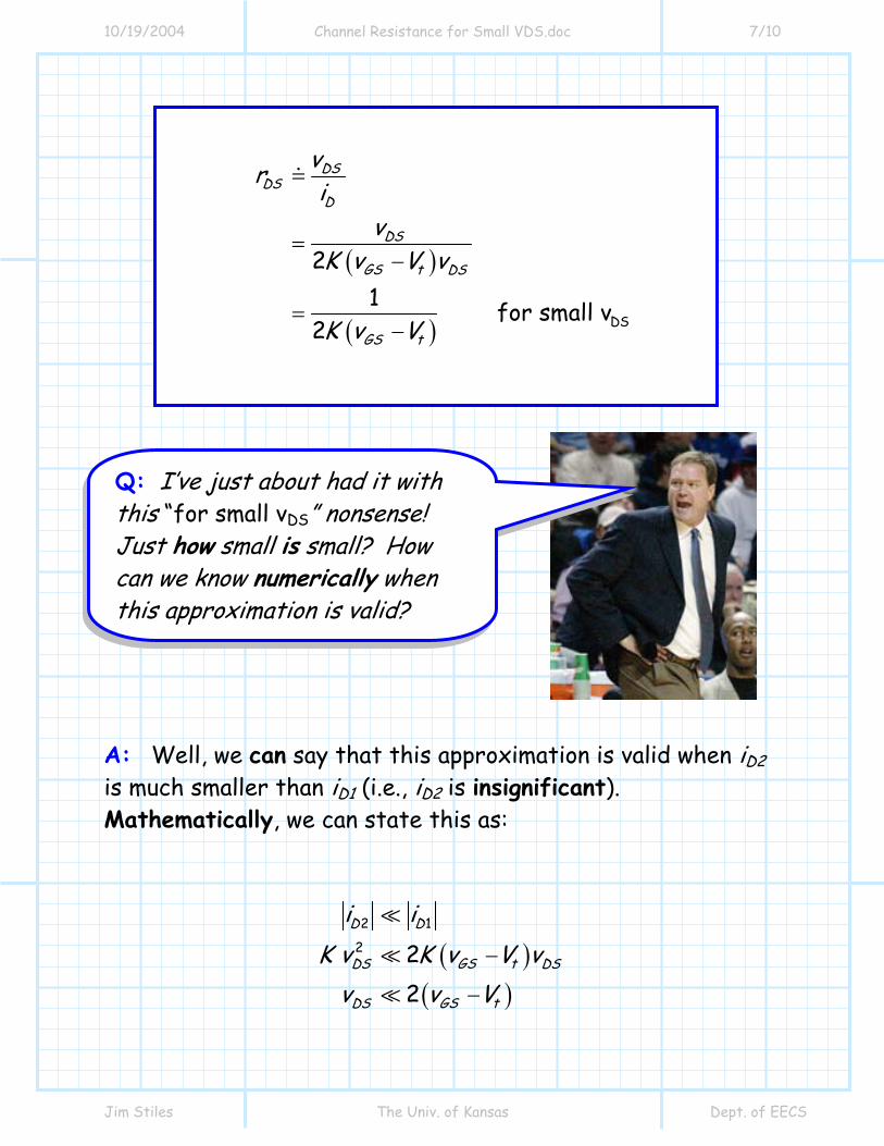
A: Well, we can say that this approximation is valid when iD2 is much smaller than iD1 (i.e., iD2 is insignificant). Mathematically, we can state this as:
( )( )
2 1
2 22
D D
GS tDS DS
GS tDS
i iK v K v V v
v v V−
−
Q: I’ve just about had it with this “for small vDS” nonsense! Just how small is small? How can we know numerically when this approximation is valid?

10/19/2004 Channel Resistance for Small VDS.doc 8/10
Jim Stiles The Univ. of Kansas Dept. of EECS
Thus, we can approximate the induced channel as a resistor rDS when vDS is much less than the twice the excess gate voltage:
( )
( ) ( )
1
DS
2
for v 2
D D
GS t DS
GS t GS tDS
i iK v V v
Wk v V v v VL
≈
= −
⎛ ⎞′= − −⎜ ⎟⎝ ⎠
and:
( )
( ) ( )( )
12
1 for 2
DSGS t
GS tDSGS t
rK v V
v v VWk v VL
=−
= −′ −
Q: There you go again! The statement ( )2 GS tDSv v V− is only slightly more
helpful than the statement “when vDS is small”. Precisely how much smaller than twice the excess gate voltage must vDS be in order for our approximation to be accurate?

10/19/2004 Channel Resistance for Small VDS.doc 9/10
Jim Stiles The Univ. of Kansas Dept. of EECS
A: We cannot say precisely how much smaller vDS needs to be in relation to 2(vGS-Vt) unless we state precisely how accurate we require our approximation to be!
For example, if we want the error associated with the approximation ( )1 2 GS tD D DSi i K v V v≈ = − to be less than 10% , we find that we require the voltage vDS to be less than 1/10 the value 2(vGS-Vt). In other words, if:
( )210 5
GS t GS tDS
v V v Vv − −< = ,
we find then that iD2 is less than 10% of iD1:
12 10
DD
ii < .
This 10% error criteria is a typical “rule-of thumb” for many approximations in electronics. However, this does not mean that it is the “correct” criteria for determining the validity of this (or other) approximation. For some applications, we might require better accuracy. For example, if we require less than 5% error, we would find that
( ) 10GS tDSv v V< − . However, using the 10% error criteria, we arrive at the conclusion that:

10/19/2004 Channel Resistance for Small VDS.doc 10/10
Jim Stiles The Univ. of Kansas Dept. of EECS
( )
( ) ( )
1
2
for 5
D D
GS t DS
GS t GS tDS DS
i iK v V v
Wk v V v v v VL
≈
= −
⎛ ⎞′= − < −⎜ ⎟⎝ ⎠
and:
( )
( ) ( )( )DS
12
1 for v 5
DSGS t
GS tGS t
rK v V
v VWk v VL
=−
= < −′ −
We find that we should use these approximations when we can—it can make our circuit analysis much easier!
See, the thing is, you should use these approximations whenever they are valid. They often make your circuit analysis task much simpler.
10/19/2004 Drain Output Resistance.doc 1/5
Jim Stiles The Univ. of Kansas Dept. of EECS
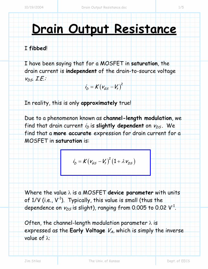
Drain Output Resistance I fibbed! I have been saying that for a MOSFET in saturation, the drain current is independent of the drain-to-source voltage vDS. I.E.:
( )2GS tDi K v V= −
In reality, this is only approximately true! Due to a phenomenon known as channel-length modulation, we find that drain current iD is slightly dependent on vDS . We find that a more accurate expression for drain current for a MOSFET in saturation is:
( ) ( )2 1GS tD DSi K v V vλ= − +
Where the value λ is a MOSFET device parameter with units of 1/V (i.e., V-1). Typically, this value is small (thus the dependence on vDS is slight), ranging from 0.005 to 0.02 V-1. Often, the channel-length modulation parameter λ is expressed as the Early Voltage VA, which is simply the inverse value of λ:

10/19/2004 Drain Output Resistance.doc 2/5
Jim Stiles The Univ. of Kansas Dept. of EECS
[ ]1 VAVλ
=
Thus, the drain current for a MOSFET in saturation can likewise be expressed as:
( )2 1 DSGS tD
A
vi K v VV
⎛ ⎞= − +⎜ ⎟
⎝ ⎠
Now, let’s define a value ID, which is simply the drain current in saturation if no channel-length modulation actually occurred—in other words, the ideal value of the drain current:
( )2GS tDI K v V−
Thus, we can alternatively write the drain current in saturation as:
1 DSD D
A
vi IV
⎛ ⎞= +⎜ ⎟
⎝ ⎠
This explicitly shows how the drain current behaves as a function of voltage vDS. For example, consider a typical case case where vDS =5.0 V and VA = 50.0 V. We find that:

10/19/2004 Drain Output Resistance.doc 3/5
Jim Stiles The Univ. of Kansas Dept. of EECS
( )
1
5 0150 0
1 0 11 1
DSD D
A
D
D
D
vi IV
.I.
I .. I
⎛ ⎞= +⎜ ⎟
⎝ ⎠⎛ ⎞= +⎜ ⎟⎝ ⎠
= +
=
In other words, the drain current is 10% larger than its “ideal” value ID.
We can thus interpret the value ADSv V as the percent increase in drain current iD over its ideal (i.e., no channel-length modulation) saturation value ( )2
GS tDI K v V= − .
Thus, as vDS increases, the drain current iD will increase slightly.
Now, let’s introduce a third way (i.e. in addition to , AVλ ) to describe the “extra” current created by channel-length modulation. Define the Drain Output Resistance ro:
1Ao
D D
VrI Iλ
=
Using this definition, we can write the saturation drain current expression as:

10/19/2004 Drain Output Resistance.doc 4/5
Jim Stiles The Univ. of Kansas Dept. of EECS
( )2
1 DSD D
A
DD DS
A
DSD
o
DSGS t
o
vi IV
II vVvIr
vK v Vr
⎛ ⎞= +⎜ ⎟
⎝ ⎠
= +
= +
= − +
Thus, we interpret the “extra” drain current (due to channel-length modulation) as the current flowing through a drain output resistor ro.

10/19/2004 Drain Output Resistance.doc 5/5
Jim Stiles The Univ. of Kansas Dept. of EECS
Finally, there are three important things to remember about channel-length modulation: * The values λ and VA are MOSFET device parameters, but drain output resistance ro is not (ro is dependent on ID!). * Often, we “neglect the effect of channel-length modulation”, meaning that we use the ideal case for saturation--iD=K(vGS-Vt)2. Effectively, we assume that 0λ = , meaning that AV = ∞ and or = ∞ (i.e., not 0AV = and 0or = !).
* The drain output resistance ro is not the same as channel resistance rDS! The two are different in many, many ways:
( )2 DSGS tD
o
vi K v Vr
= − + for a MOSFET in saturation
DS
DDS
vir
= for a MOSFET in triode and vDS small
!!!!!!!o DSr r∴ ≠
10/19/2004 The Body Effect.doc 1/3
Jim Stiles The Univ. of Kansas Dept. of EECS
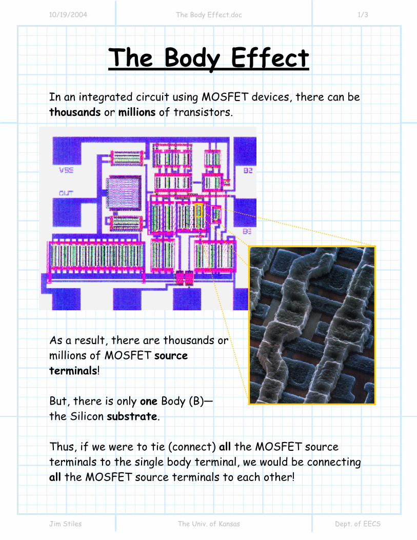
The Body Effect In an integrated circuit using MOSFET devices, there can be thousands or millions of transistors. As a result, there are thousands or millions of MOSFET source terminals! But, there is only one Body (B)—the Silicon substrate. Thus, if we were to tie (connect) all the MOSFET source terminals to the single body terminal, we would be connecting all the MOSFET source terminals to each other!

10/19/2004 The Body Effect.doc 2/3
Jim Stiles The Univ. of Kansas Dept. of EECS
This would almost certainly result in a useless circuit! Thus, for integrated circuits, the MOSFET source terminals are not connected to the substrate body.
A: We must consider the MOSFET Body Effect! We note that the voltage vSB (voltage source-to-body) is not necessarily equal to zero (i.e., 0SBv ≠ )! Thus, were back to a four-terminal MOSFET device. There are many ramifications of this body effect; perhaps the most significant is with regard to the threshold voltage Vt. We find that when 0SBv ≠ , a more accurate expression of the threshold voltage is:
0 2 2t t SBf fV V vγ φ γ φ= + + −
where γ and fφ are MOSFET device parameters.
Q: Yikes! What happens to MOSFET behavior if the source is not attached to the body ??
10/19/2004 The Body Effect.doc 3/3
Jim Stiles The Univ. of Kansas Dept. of EECS
Note the value Vt0 is the value of the threshold voltage when vSB = 0, i.e.:
0 when 0 0t t SBV V v .= =
Thus, the value Vt0 is simply the value of the device parameter Vt that we have been calling the threshold voltage up till now! In other words, Vt0 is the value of the threshold voltage when we ignored the Body Effect, or when vSB = 0. It is thus evident that the term:
2 2SBf fvγ φ γ φ+ −
simply expresses an extra value added to the “ideal” threshold voltage Vt0 when 0SBv ≠ .
For many cases, we find that this Body Effect is relatively insignificant, so we will (unless otherwise stated) ignore the Body Effect. However, do not conclude that the Body Effect is always insignificant—it can in some cases have a tremendous impact on MOSFET circuit performance!