
4.1 GaAs Wafer Breakage Reduction · wafer breakage and strength reduction is a function of process...
4
GaAs Wafer Breakage Reduction Bruce Darley, Manjeet Singh, Patrick Santos, Ernesto Ambrocio and Shiban Tiku Skyworks Solutions Inc., Newbury Park, CA 91320 [email protected], 805-480-4302 Keywords: Wafer Breakage, GaAs Wafers, Yield Abstract We present results of many years of work for breakage reduction of GaAs wafers at Skyworks. Incoming wafers are seen to be strong. Micro-scratches and micro-cracks added during processing reduce the strength of processed wafers. However, wafer strength reduction is not linear and breakage rate does not increase simply by adding fabrication steps. Instead, wafer breakage and strength reduction is a function of process and tool type. Wafers may break at a tool or weakened wafers may break later. Once attention is given to the main culprits and issues resolved, breakage goes down. A few specific examples will be described. INTRODUCTION GaAs wafer breakage has been accepted as a norm because of the extreme brittleness of wafers [1-3]. Historically, in the three inch wafer size days, 18% rate was not unusual. As the volume and size of the wafers grew, high rates became unacceptable. Today, using 150 mm (6 inch) wafers, the raw material cost has dropped significantly due to the high volume, but epi wafers are invariably used for commonly used III-V products. Therefore, finished product wafer cost remains a challenge. Breakage rates had settled down at about 2% in the last decade. The run rates are in thousands of wafer per week. Fab yields are running around 95 % and probe yields are approaching 99 %. At a breakage rate of 2%, it is the highest Pareto item among the causes of yield loss. Skyworks has reduced breakage levels from a few percent to below 0.5% (measured as wafers broken as a fraction of wafer outs plus wafers broken). Fig. 1 shows the reduction of wafer breakage over a few years’ time. Fab- wide initiatives and improvements to achieve this reduction are discussed in this paper. This rate does not include operator errors that result in whole-lot breakage. Only minor breakage defined as breakage of fewer than five wafers per event are included in the current study. Wafer Strength Determination Historically substrate defects from boule growth to substrate processing and epi stress contributed to breakage later during circuit fabrication. These have been reduced to negligible levels. Our measurements of wafer strength of incoming epi wafers confirms this. Fig. 1: Wafer breakage drop over the last few years at Skyworks. In order to quantify and track loss of wafer strength as the wafers are processed through different stages and different tools, we used a fracture testing method used by others in the past [1,3]. In this method wafers are placed face up in a circular jig and a stylus is applied to the center. Force is then applied with the stylus. A predetermined contact speed and rate of increase of applied force are controlled while measuring the stylus force in the center of the wafer. The max force on a digital display is kept by the tool at the time of wafer breakage. We record this value along with other known pertinent information such as wafer stage or wafer thickness. Fig. 2 shows the schematic diagram of the apparatus. An example of the wafer strength data of incoming wafers is shown in Fig. 3. The median strength of the wafers is 11.2 lbs., and the strongest wafers read: 23.5 lbs. These strength measurements indicate that the starting wafers are acceptable and the breakage must be caused by damage and subsequent weakening during the processing. The type of break we see most often is a straight line crack See Fig. 4. Investigation of chips or nicks that may have initiated the break revealed that there is generally no evidence present at the edge. It has been known that micro-cracks on the backside of the wafer and chips around the edges cause the wafer strength to drop significantly. Wafers can be damaged at one stage and break later in the process. In many instances, an increase in breakage at one stage can be tracked to an earlier stage by tool commonality analysis. For example, wafers breaking in 4 53 CS MANTECH Conference, May 19th - 22nd, 2014, Denver, Colorado, USA
Transcript of 4.1 GaAs Wafer Breakage Reduction · wafer breakage and strength reduction is a function of process...
GaAs Wafer Breakage Reduction
Bruce Darley, Manjeet Singh, Patrick Santos, Ernesto Ambrocio and Shiban Tiku
Skyworks Solutions Inc., Newbury Park, CA 91320
[email protected], 805-480-4302
Keywords: Wafer Breakage, GaAs Wafers, Yield
Abstract
We present results of many years of work for
breakage reduction of GaAs wafers at Skyworks.
Incoming wafers are seen to be strong. Micro-scratches
and micro-cracks added during processing reduce the
strength of processed wafers. However, wafer strength
reduction is not linear and breakage rate does not
increase simply by adding fabrication steps. Instead,
wafer breakage and strength reduction is a function of
process and tool type. Wafers may break at a tool or
weakened wafers may break later. Once attention is
given to the main culprits and issues resolved, breakage
goes down. A few specific examples will be described.
INTRODUCTION
GaAs wafer breakage has been accepted as a norm
because of the extreme brittleness of wafers [1-3].
Historically, in the three inch wafer size days, 18% rate was
not unusual. As the volume and size of the wafers grew, high
rates became unacceptable. Today, using 150 mm (6 inch)
wafers, the raw material cost has dropped significantly due
to the high volume, but epi wafers are invariably used for
commonly used III-V products. Therefore, finished product
wafer cost remains a challenge. Breakage rates had settled
down at about 2% in the last decade. The run rates are in
thousands of wafer per week. Fab yields are running around
95 % and probe yields are approaching 99 %. At a breakage
rate of 2%, it is the highest Pareto item among the causes of
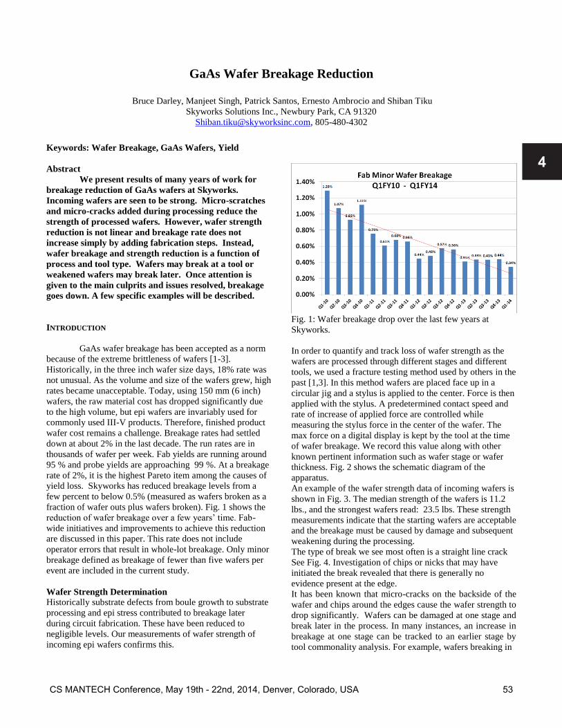
yield loss. Skyworks has reduced breakage levels from a
few percent to below 0.5% (measured as wafers broken as a
fraction of wafer outs plus wafers broken). Fig. 1 shows the
reduction of wafer breakage over a few years’ time. Fab-
wide initiatives and improvements to achieve this reduction
are discussed in this paper. This rate does not include
operator errors that result in whole-lot breakage. Only minor
breakage defined as breakage of fewer than five wafers per
event are included in the current study.
Wafer Strength Determination
Historically substrate defects from boule growth to substrate
processing and epi stress contributed to breakage later
during circuit fabrication. These have been reduced to
negligible levels. Our measurements of wafer strength of
incoming epi wafers confirms this.
Fig. 1: Wafer breakage drop over the last few years at
Skyworks.
In order to quantify and track loss of wafer strength as the
wafers are processed through different stages and different
tools, we used a fracture testing method used by others in the
past [1,3]. In this method wafers are placed face up in a
circular jig and a stylus is applied to the center. Force is then
applied with the stylus. A predetermined contact speed and
rate of increase of applied force are controlled while
measuring the stylus force in the center of the wafer. The
max force on a digital display is kept by the tool at the time
of wafer breakage. We record this value along with other
known pertinent information such as wafer stage or wafer
thickness. Fig. 2 shows the schematic diagram of the
apparatus.
An example of the wafer strength data of incoming wafers is
shown in Fig. 3. The median strength of the wafers is 11.2
lbs., and the strongest wafers read: 23.5 lbs. These strength
measurements indicate that the starting wafers are acceptable
and the breakage must be caused by damage and subsequent
weakening during the processing.
The type of break we see most often is a straight line crack
See Fig. 4. Investigation of chips or nicks that may have
initiated the break revealed that there is generally no
evidence present at the edge.
It has been known that micro-cracks on the backside of the
wafer and chips around the edges cause the wafer strength to
drop significantly. Wafers can be damaged at one stage and
break later in the process. In many instances, an increase in
breakage at one stage can be tracked to an earlier stage by
tool commonality analysis. For example, wafers breaking in
4
53CS MANTECH Conference, May 19th - 22nd, 2014, Denver, Colorado, USA

Fig. 2: Schematic diagram of wafer strength measurement.
Fig. 3: Distribution of incoming wafer strength
the Novellus nitride deposition system may break due to
damage caused at an earlier stage by a lift-off tool.
The scratches that cause breakage can be micro scratches,
like unintentional, very small scribe lines less than a
centimeter long. Edge chips can be caused by collisions of
wafers with metal cassettes and quartz boats, alignment pins
on equipment, and wafers hitting objects due to accidental
handling errors. Pressure or load on wafers due to chucks
under vacuum or electrostatic force can cause breakage if the
wafers are already scratched.
Wafer strength reduction as the wafers go through the fab is
plotted by stage in Fig: 5. One would intuitively suspect that
the wafers should get weaker as the fabrication damage is
accumulated. However, data indicate progressive
weakening by processing alone is negligible. The majority of
wafer weakening occurs from other factors like damage at
specific tools, including micro-scratches, thermal stresses
and vibration.
Micro-crack Generation Experiments
In order to study the effect of micro-cracks and determine
the critical size of cracks, the following procedure was used.
Wafers were scratched with lapping film coated with
diamond particles and applying a rubber roller to produce
micro-scratches as seen in Fig.6. Fig. 7 shows an optical
Fig.4: Different types of breaks, weak and strong wafers.
Fig.5: Breakage strength at different stages in the
fabrication process.
microscope picture of micro-scratches, similar to those
present on the back side of actual wafers. The results from
this study showed that even a few millimeter long scratches
of depth as shallow as 0.15 m can cause breakage.
Although the scratch may be only sub- micron deep, the
micro crack created by this scratch can be very deep.
54 CS MANTECH Conference, May 19th - 22nd, 2014, Denver, Colorado, USA

Fig. 6: Inducing microscatches on wafer backside
Fig. 7: Optical Microscope view of micro scratches on the
backside of wafer
Fig. 8 shows the FIB (focused- ion beam) cross-section.
With the addition of micro scratches, the wafer strength
dropped as shown in Fig. 9. Therefore, micro-scratches must
be avoided in the GaAs IC fabrication process.
Manual Handling of Wafers
There are process steps that have not been automated due to
prohibitive cost or space limitations. The major example is
the loading of wafers into metal evaporators that are
essential to III-V processing. Automatic loaders for loading
wafers on evaporator domes are huge and take a lot of space
in the fab isle. So, wafers must be loaded by operators. Since
the dome is metallic and 20 wafers must be loaded within a
short time (due to close couple requirements), the operator
may rush, causing wafers to break or chip. Operator training
is essential here. Also, manual shuffling of wafers within
the cassette is often done. For example when wafers are
loaded into the nitride deposition tool they arrive in slots 6-
25 of the cassette and are shifted to slots 1-20.
Or, when two 10 wafer lots will be combined into one
Fig.8: FIB Cross section of a micro-scratch showing sub-
surface damage.
Fig. 9: Wafer strength drop after addition of micro scratches
cassette for better tool use efficiency they are manually
handled. Vacuum wands weaken a wafer every time these
touch a wafer. Also, any time a wand is rubbed across the
surface (prior to vacuum being applied) it can cause micro
scratches.
“Silent processing” is a general rule for GaAs fabs. Even for
wafer transport within the fab, carts must be properly
designed to avoid wafer bouncing in the cassettes.
Vibrations through the cassette as the lot box is pushed
across a shelf (made of parallel wires) can weaken wafers.
Transport of wafers (while in lot boxes) on carts also add
vibrations. These vibrations were measured with an
accelerometer while pushing carts (with wafers) over a
smooth floor, grated metal floor, thresholds in doorways,
rubber pads with raised bump surface, ramp zones etc. “G”
forces were recorded on X, Y, Z axis with a perfect baseline
(zero vibration) being 0,0,-1 for X,Y,Z respectively. Not
surprisingly, the Z axis measured the most vibration.
Different carts with different wheels performed differently.
Soft large wheels were the best. Carts with built in shock
absorption in the chassis also help. As expected, thresholds
and bumpy surfaces produced higher “G” forces
(vibrations). Max “G” force (vibration) values ranged from
0.45 to 0.94 G’s when pushing carts at a normal walking
speed.
4
55CS MANTECH Conference, May 19th - 22nd, 2014, Denver, Colorado, USA

How the Breakage Rate was Reduced
Breakage data are collected on a daily basis by a problem lot
disposition system. Process step, tool, description and cause
if known are captured. The data are reported to Process and
Equipment engineering. Any repeat offenders are
immediately identified and put down for root cause
determination and repair. Test wafers are cycled through
before the tool is returned to production. Long term data are
analyzed and plotted in different ways. Fig.10 shows an
example of the breakage rate at different stages of
processing. As expected, based on the wafer strength data,
the rate does not go up with stage.
Fig.10: Breakage rates at different stages of GaAs wafer
processing. Breakage rate does not go up as the wafers
progress through the process.
The most obvious way to look at the data is an equipment
Pareto. It is clear from the Pareto study that a few tool sets
are responsible for the majority of the breakage. Fig. 11
shows a typical Pareto chart. The highest breakage rate is
from manual handling, so automated handling is done as
much as possible.
The highest automated handler breakage rate is caused by
tools using handlers with high-speed rotation, high pressure
spray, wafer grippers, etc. Since manual handling and the
associated breakage have been minimized, we have seen the
automatic wafer handlers start showing up on the Pareto
chart. As soon as a tool handler was identified, steps were
taken to find the cause and modifications were made. As an
example, the SSEC tools that were the worst offender, were
modified. Taller retainers to prevent wafers from being
misplaced have improved the breakage dramatically. In
another case, handling errors were traced to a single part, a
rotation potentiometer, which was replaced by a more robust
part. Also on the same tool, cassette tables were re-leveled to
wafer chuck and breakage rate dropped. Modifications were
Fig.11: Pareto of breakage by tool.
made on other wafer handlers, wafer sorters, transfer tools,
aligners, cassettes, vacuum wands etc.
Conclusion
Micro-scratches and damage must be avoided for reduction
of wafer breakage in general. For reduction of breakage to
very low levels, attention to specific root causes is essential.
Wafer breakage has been found to be strongly determined by
specific tool and process and not by general weakening of
wafers as they progress through the process. Wafer breakage
can be reduced by regular monitoring and feedback to
equipment and process engineers. The result of these efforts
has been the reduction of breakage to the current level of
0.4% over a period of a few years as seen in Fig. 1. Wafer
breakage reduction is an on-going process. However,
making further gains is going to be harder and cost a bit
more in tool modifications and automation.
References
1. T. Cordner and B. Marks, “GaAs Breakage , Causes,
Cures, Growth and Process”, GaAs IC Symposium, 317,
(1993).
2. S. Wdowik, “ Reduction of Wafer Breakage in a 4 inch
GaAs Wafer Fab Facility through the Implementation of a
Biaxial Stress Test”, GaAS MANTECH, (1990).
3. M. Schaper et. al., “ Fracture Mechanical Evaluation of
GaAs Wafers”, Progress in Semiconductors II, Electronics
and Optoelectronics, 744, MRS Proceedings (2002).
ACKNOWLEDGEMENTS
All the Fab operations personnel at Skyworks were involved
in this effort and deserve acknowledgment. The authors
would like to thank Catherine Luo, Chad Davies, Heather
Knoedler, Nercy Ebrahimi, Homan Khaki, Jens Riege, and
Steve Nial in particular for directly contributing to this
effort.
56 CS MANTECH Conference, May 19th - 22nd, 2014, Denver, Colorado, USA


![M. Reiche 1, a · silicon wafer bonding about 20 years ago [ 19 -21 ]. Semiconductor wafer direct bon ding (SWDB) requires wafers with a high degree of flatness, parallelism and smoothness.](https://static.fdocuments.in/doc/165x107/5fc86cb200b94d4d71210cba/m-reiche-1-a-silicon-wafer-bonding-about-20-years-ago-19-21-semiconductor.jpg)


