Common Base Amplifier with 7- dB gain at 176 GHz in InP mesa DHBT Technology
date post
22-Dec-2015Category
view
218download
0
40 GHz MMIC Power Amplifier in InP DHBT Technology
Y.Wei, S.Krishnan, M.Urteaga, Z.Griffith, D.Scott,
V.Paidi, N.Parthasarathy, M.Rodwell
Department of Electrical and Computer Engineering, University of California
[email protected] tel: 805-893-8044, fax 805-893-3262
OutlineLEC 2002 UCSB
• Introduction• Transferred-Substrate Power DHBT Technology• Circuit Design• Results• Conclusion

Introduction LEC 2002
• Applications for power amplifiers in Ka band satellite communication systems wireless LANs local multipoint distribution system
personal communications network links and digital radio
• MMIC Amplifiers in this frequency band
Kwon et. al., IEEE MTT, Vol.48, No. 6, June. 2000
3 stage HEMT, class AB, Pout=1 W, Gain=15 dB, PAE=28.5%, size=9.5 mm2
• This Work:
Single stage cascode InP DHBT, class A, Pout=50 mW, Gain=7 dB, PAE=12.5% size=0.42 mm2

Transferred-Substrate HBT MMIC fabrication

MBE DHBT layer structure
Band profile at Vbe=0.7 V, Vce=1.5 V
InP 8E17 Si 300 Å
emitter
InGaAs 1E19 Si 500 Å
Grade 1E19 Si 200 Å
InP 1E19 Si 900 Å
Grade 8E17 Si 233 Å
Grade 2E18 Be 67 Å
InGaAs 4E19 Be 400 Å
Grade 1E16 Si 480 Å
InP 2E18 Si 20 Å
InP 1E16 Si 2500 Å
Multiple stop etch layers
Buffer layer 2500 Å
base collector
substrate
400 Å InGaAs base3000 Å InP collector

0
10
20
30
40
1 10 100 1000
Gai
ns (
dB)
Frequency (GHz)
U
h21 462
395
343
139
Small-area T.S. DHBTs have high cutoff frequencies.
UCSBSangmin Lee
0.0
1.0
2.0
3.0
0 1 2 3 4 5 6 7 8 9
Vce(V)
Ic(m
A)
BVCEO = 8 V at JE =0.4 mA/m2
fmax = 462 GHz, ft = 139 GHz
Vce(sat) ~1 V at 1.8 mA/m2

Design difficulties with large-area power DHBTs UCSBYun Wei
ARO MURI
Thermal instability further increasescurrent non-uniformity
Ic
Temperature
collector
SiNemitter
contactbase poly
BCBBCB Metal strip
Au Via
Steady state current and temperature distribution when thermally stable
base feed sheet resistance:
s= 0.3 / �significant for > 8 um emitter finger length
Large Area HBTs: big Ccb, small Rbb,
even small excess Rbb
substantially reduces fmax
0.08 m
Emitter contactMetal1
Base contact
Current hogging in multi-finger DHBT:
Distributed base feed resistance:
Ic
Temperature
K<1 for thermal stability→ must add emitter ballast resistance
Initial current and temperature distribution
thermal feedback further increases current non-uniformity
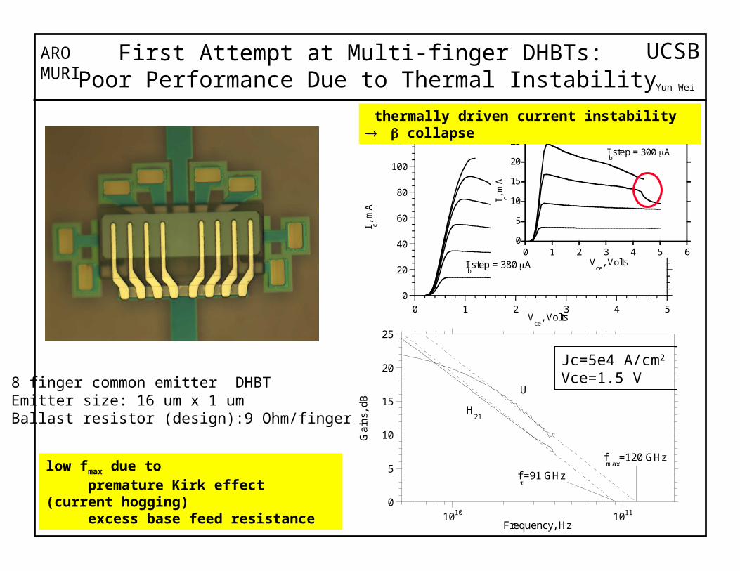
8 finger common emitter DHBTEmitter size: 16 um x 1 um Ballast resistor (design):9 Ohm/finger
0
20
40
60
80
100
120
0 1 2 3 4 5
I c, m
A
Vce
, Volts
Ibstep = 380 A
0
5
10
15
20
25
0 1 2 3 4 5 6
I c, m
A
Vce
, Volts
Ibstep = 300 A
0
5
10
15
20
25
1010 1011
Ga
ins,
dB
Frequency, Hz
H21
U
fmax
=120 GHz
f=91 GHz
Jc=5e4 A/cm2
Vce=1.5 V
First Attempt at Multi-finger DHBTs: Poor Performance Due to Thermal Instability
thermally driven current instability collapse
UCSB
low fmax due to premature Kirk effect (current hogging) excess base feed resistance
ARO MURI
Yun Wei

Large Current High Breakdown Voltage Broadband InP DHBT
UCSB
8 -finger DHBT8 x (1 m x 16 m emitter )8 x (2 m x 20 m collector )
Key Improvements8 Ohm ballast per emitter finger2nd-level base feed metal
Device Performancefmax>330 GHz, Vbrceo>7 V,Jmax>1x10⁵ A/cm2
100 mA, 3.6 Volt device
2nd-level base feed metal
Ballast resistor
emitter
collector
Flip chip
Yun Wei
ARO MURI

UCSBHBT power amplifier-why cascode?
ARO MURI
Yun Wei
IB1
* R. Ramachandran and A.F. Podell "Segmented cascode HBT for microwave-frequency power amplifiers"
Advantages:common-base stage has large Vce
→ large output power common-emitter-stage has low Vce
→ small Rballast required
→ maintains large available power gain
Disadvantageinductance of base bypass capacitoreven small L greatly degrades gain
Vce1
Vce2
+-+
-IE1
Rballast
IE2
radial stub capacitor
common basestage mesa
common emitterstage mesa
bias 2 bias 3
bias 1

UCSBInP TS DHBT Power Amplifier Design
ARO MURI
Yun Wei
Optimum admittance match
Input match
Low frequency stabilization
4 parallel cascode amplifier
4 parallel cascode amplifier
8 finger cascodeInter-stage
DC bias
/4
/4
Imax
0.0 0.5 1.0 1.5 2.0 2.5 3.0 3.5 4.0 4.5 5.0 5.5 6.0 6.5 7.0
Vce (V)
0.000
0.002
0.004
0.006
0.008
0.010
0.012
0.014
0.016
0.018
Ic (
A)
VCE_BRVsat

40 GHz 128 m2 power amplifier UCSB
cascode PA
0.6mm x 0.7 mm, AE=128 m2
ARO MURI
f0=40 GHz
BW3dB=16 GHz
GT=7 dB
P1dB=14 dBm
Psat=17 dBm @ 4dB gain
-40
-30
-20
-10
0
10
20 25 30 35 40 45
Sij,
dB
Frequency, GHz
S21
S11
S22
-5
0
5
10
15
20
0
2
4
6
8
10
12
14
-15 -10 -5 0 5 10 15
Po
ut,
GT,
dB
m
PA
E, %
Pin, dBm
GT
Pout
PAE
Yun Wei

UCSBYun Wei
common base PA
-5
0
5
10
15
20
0
2
4
6
8
10
-15 -10 -5 0 5 10 15
Po
ut,
dB
m GT , d
B
Pin, dBm
GT Pout
-30
-25
-20
-15
-10
-5
0
5
10
80 90 100 110
S11
, S
21,
S22
frequency, GHz
S21
S22
S11
0.5mm x 0.4 mm, AE=128 m2
ARO MURI
Bias: Ic=78 mA, Vce=3.6 V
f0=85 GHz
BW3dB=28 GHz
GT=8.5 dB
P1dB=14.5 dBm
Psat=16dBm, associated gain: 4.5 dB
Y. Wei et al, 2002 IEEE MTT-S symposium
W band power amplifiers in TS InP DHBT technology
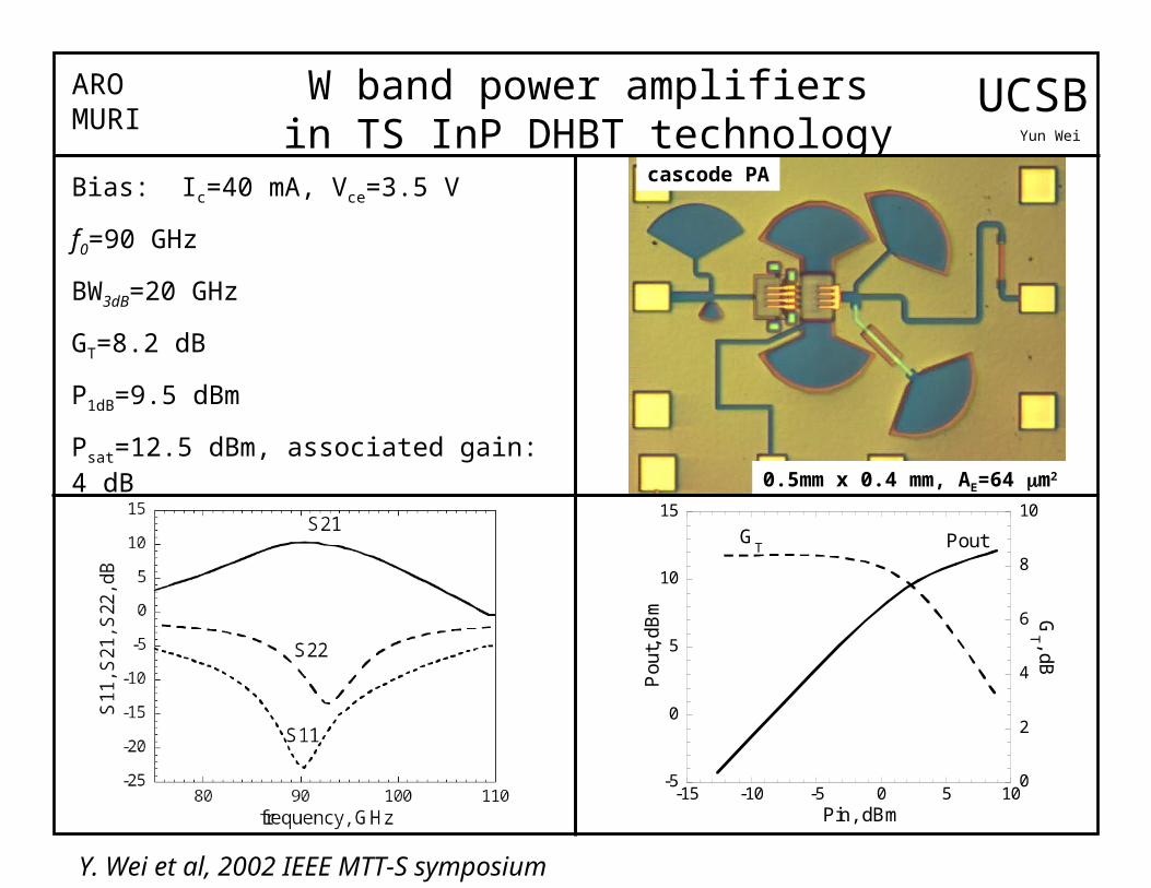
W band power amplifiers in TS InP DHBT technology
UCSBYun Wei
cascode PA
0.5mm x 0.4 mm, AE=64 m2
ARO MURI
-5
0
5
10
15
0
2
4
6
8
10
-15 -10 -5 0 5 10
Po
ut, d
Bm G
T , dB
Pin, dBm
GT Pout
Bias: Ic=40 mA, Vce=3.5 V
f0=90 GHz
BW3dB=20 GHz
GT=8.2 dB
P1dB=9.5 dBm
Psat=12.5 dBm, associated gain: 4 dB
Y. Wei et al, 2002 IEEE MTT-S symposium

Continuing work
Higher-current DHBTs for increased mm-wave output power250 GHz fmax, Ic,max=240 mA, thermally stable at 200 mA bias at Vce=3.2 Volts→ suitable for W-band ~150 mW power amplifiers
W-band DHBT power amplifiersdesigns for > 100 mW saturated output power now being tested
Results to be reported subsequently…
UCSB
Yun WeiLEC 2002
Conclusions
• 40 GHz MMIC power amplifier in InP DHBT technology
7 dB power gain and 14 dBm output power at 1 dB compression. 17 dBm (50 mW) saturated output power 12.5% peak power added efficiency
Future work: higher power DHBT power amplifiers at W-band and above
lumped 4-finger topology, longer emitter fingers, power combining
G-band (140-220 GHz) DHBT power amplifiers
Acknowledgement
Work funded by ARO-MURI program under contract number PC249806.
UCSB
Yun WeiLEC 2002