3D Time-of-flight distance measurement with custom solid ... · the use of CMOS, all commonly known...
223
3D Time-of-flight distance measurement with custom solid-state image sensors in CMOS/CCD-technology 3D Time-of-flight distance measurement with custom solid-state image sensors in CMOS/CCD-technology Robert Lange Robert Lange
Transcript of 3D Time-of-flight distance measurement with custom solid ... · the use of CMOS, all commonly known...
3D Time-of-flight distance measurementwith custom solid-state image sensors
in CMOS/CCD-technology
3D Time-of-flight distance measurementwith custom solid-state image sensors
in CMOS/CCD-technology
Robert LangeRobert Lange
3D Time-of-Flight Distance Measurement with Custom Solid-State Image Sensors in
CMOS/CCD-Technology
A dissertation submitted to the
DEPARTMENT OF ELECTRICAL ENGINEERING AND
COMPUTER SCIENCE AT UNIVERSITY OF SIEGEN
for the degree of
DOCTOR OF TECHNICAL SCIENCES
presented by
Dipl.-Ing. Robert Lange
born March 20, 1972
accepted on the recommendation of
Prof. Dr. R. Schwarte, examiner
Prof. Dr. P. Seitz, co-examiner
Submission date: June 28, 2000
Date of oral examination: September 8, 2000

To my parents
3D Distanzmessung nach dem „Time-of-Flight“- Verfahren mit
kundenspezifischen Halbleiterbildsensoren in CMOS/CCD Technologie
VOM FACHBEREICH ELEKTROTECHNIK UND INFORMATIK
DER UNIVERSITÄT-GESAMTHOCHSCHULE SIEGEN
zur Erlangung des akademischen Grades
DOKTOR DER INGENIEURWISSENSCHAFTEN
(DR.-ING.)
genehmigte Dissertation
vorgelegt von
Dipl.-Ing. Robert Lange
geboren am 20. März 1972
1. Gutachter: Prof. Dr.-Ing. R. Schwarte
2. Gutachter: Prof. Dr. P. Seitz
Vorsitzender der Prüfungskommission: Prof. Dr.-Ing H. Roth
Tag der Abgabe: 28. Juni 2000
Tag der mündlichen Prüfung: 8. September 2000

Meinen Eltern

I
Contents
Contents .................................................................................................................... I
Abstract ....................................................................................................................V
Kurzfassung............................................................................................................IX
1. Introduction.......................................................................................................... 1
2. Optical TOF range measurement ....................................................................... 9
2.1 Overview of range measurement techniques.......................................... 11
2.1.1 Triangulation ................................................................................... 11
2.1.2 Interferometry.................................................................................. 13
2.1.3 Time-of-flight ................................................................................... 16
2.1.4 Discussion....................................................................................... 24
2.2 Measuring a signal’s amplitude and phase ............................................. 26
2.2.1 Demodulation and sampling ........................................................... 26
2.2.2 Aliasing ........................................................................................... 36
2.2.3 Influence of system non-linearities ................................................. 46
2.2.4 Summary......................................................................................... 47
3. Solid-state image sensing ................................................................................ 49
3.1 Silicon properties for solid-state photo-sensing....................................... 52
3.1.1 Photodiodes in CMOS .................................................................... 52
3.1.2 MOS photogate............................................................................... 57
3.1.3 Transport mechanisms for charge carriers ..................................... 62
3.1.4 Noise sources ................................................................................. 68
3.1.5 Sensitivity and Responsivity ........................................................... 71
3.1.6 Optical fill factor .............................................................................. 72
3.2 Charge coupled devices: CCD - basic principles .................................... 73
3.3 Active pixel sensors: CMOS APS............................................................ 81
3.4 Discussion ............................................................................................... 83

II
4. Power budget and resolution limits................................................................. 85
4.1 Optical power budget............................................................................... 85
4.2 Noise limitation of range accuracy........................................................... 90
5. Demodulation pixels in CMOS/CCD................................................................. 99
5.1 Pixel concepts ....................................................................................... 102
5.1.1 Multitap lock-in CCD ..................................................................... 102
5.1.2 4-tap lock-in pixel .......................................................................... 104
5.1.3 1-tap lock-in pixel .......................................................................... 109
5.1.4 Summary: Geometry and speed performance.............................. 113
5.2 Characterization of 1-tap pixel performance.......................................... 116
5.2.1 Charge to voltage conversion ....................................................... 116
5.2.2 Measurement setup, expectations and predictions ...................... 120
5.2.3 Determination of optimal control voltages..................................... 130
5.2.4 Influence of optical power and integration time @ 20 MHz .......... 134
5.2.5 Demodulation contrast versus frequency and wavelength ........... 137
5.2.6 Phase accuracy measurements ................................................... 139
5.2.7 Noise performance and dynamic range........................................ 142
5.2.8 Comparison of measured distance accuracy with theory ............. 143
5.2.9 Summary....................................................................................... 145
5.3 Outlook: Two-photosite demodulation pixel .......................................... 147

III
6. Imaging TOF range cameras .......................................................................... 151
6.1 Camera electronics................................................................................ 152
6.1.1 Digital sequencer board................................................................ 152
6.1.2 Driving electronics board .............................................................. 155
6.1.3 Modulated illumination .................................................................. 158
6.2 2D range camera................................................................................... 159
6.2.1 108 pixel lock-in line sensor.......................................................... 159
6.2.2 System architecture ...................................................................... 163
6.2.3 2D range measurement ................................................................ 167
6.3 3D range camera................................................................................... 169
6.3.1 64 x 25 pixel lock-in image sensor................................................ 169
6.3.2 System architecture ...................................................................... 171
6.3.3 3D range measurement ................................................................ 173
6.4 Discussion ............................................................................................. 180
7. Summary and Perspective.............................................................................. 181
8. Appendix .......................................................................................................... 187
8.1 Physical constants................................................................................. 187
8.2 Typical parameters of a 2 µm CMOS technology.................................. 188
8.3 Conversion: LUMEN, WATT and CANDELA......................................... 189
8.4 Measurement conditions (MCD) for Chapter 5...................................... 191
References ........................................................................................................... 195
Acknowledgments............................................................................................... 203
Curriculum Vitae.................................................................................................. 205
UB Siegen
Anmerkung der UB Siegen Einen Anschauungsfilm zur Dissertation finden Sie unter der URL: http://www.ub.uni-siegen.de/pub/diss/fb12/2000/lange/3D_movie.exe

V
Abstract
Since we are living in a three-dimensional world, an adequate description of our
environment for many applications includes the relative position and motion of the
different objects in a scene. Nature has satisfied this need for spatial perception by
providing most animals with at least two eyes. This stereo vision ability is the basis
that allows the brain to calculate qualitative depth information of the observed
scene. Another important parameter in the complex human depth perception is our
experience and memory. Although it is far more difficult, a human being is even
able to recognize depth information without stereo vision. For example, we can
qualitatively deduce the 3D scene from most photos, assuming that the photos
contain known objects [COR].
The acquisition, storage, processing and comparison of such a huge amount of
information requires enormous computational power - with which nature fortunately
provides us. Therefore, for a technical implementation, one should resort to other
simpler measurement principles. Additionally, the qualitative distance estimates of
such knowledge-based passive vision systems can be replaced by accurate range
measurements.
Imaging 3D measurement with useful distance resolution has mainly been realized
so far with triangulation systems, either passive triangulation (stereo vision) or
active triangulation (e.g. projected fringe methods). These triangulation systems
have to deal with shadowing effects and ambiguity problems (projected fringe),
which often restrict the range of application areas. Moreover, stereo vision cannot
be used to measure a contrastless scene. This is because the basic principle of
stereo vision is the extraction of characteristic contrast-related features within the
observed scene and the comparison of their position within the two images. Also,
extracting the 3D information from the measured data requires an enormous time-
consuming computational effort. High resolution can only be achieved with a
relatively large triangulation base and hence large camera systems.
VI
A smarter range measurement method is the TOF (Time-Of-Flight) principle, an
optical analogy to a bat’s ultrasonic system rather than human’s stereo vision. So
far TOF systems are only available as 1D systems (point measurement), requiring
laser scanners to acquire 3D images. Such TOF scanners are expensive, bulky,
slow, vibration sensitive and therefore only suited for restricted application fields.
In this dissertation an imaging, i.e. non-scanning TOF-camera is introduced, based
on an array of demodulation pixels, where each pixel can measure both the
background intensity and the individual arrival time of an RF-modulated (20 MHz)
scene illumination with an accuracy of a few hundreds of picoseconds (300⋅10-12 s).
The pixel’s working concept is based on the CCD principle (Charge Coupled
Device), allowing the transportation, storage and accumulation of optically
generated charge carriers to defined local sites within the imaging device. This
process is extremely fast and essentially loss-free. We call our new, powerful high-
functionality pixels demodulation pixels because they extract the target’s distance
and reflectivity from the received optical signal. This extracted information is
modulated into the active optical signal during the time of propagation of the light
(or time of flight) through the observed scene. Each pixel works like an individual
high-precision stopwatch, and since its realization is mainly based on CMOS
technology this new technique will benefit from the ongoing technology
developments in terms of improved time- and hence distance resolution. Thanks to
the use of CMOS, all commonly known CMOS APS (Active Pixel Sensor) features
(Regions Of Interest addressing: ROI, AD conversion, etc.) can be implemented
monolithically in the future.
The imaging devices have been fabricated in a 2 µm CMOS/CCD process, a
slightly modified CMOS process which is available as an inexpensive prototyping
service (Multi Project Wafer: MPW). This process offers the freedom to implement
CCDs with sufficiently good performance for our application, although the
performance is inferior to dedicated CCD technologies. We have realized and
characterized several different pixel structures and will present these results here.
The demodulation pixel with the best fill-factor and demodulation performance has
been implemented (1) as a line sensor with 108 pixels and (2) as an image sensor
with 64 x 25 pixels. Both devices have been integrated in separate range cameras
working with modulated LED illumination and covering a distance range of 7.5 up to
15 meters. For non-cooperative diffusely reflecting targets these cameras achieve
VII
centimeter accuracy. With the single exception of the demodulation pixel array
itself, only standard electronic and optical components have been used in these
range cameras. For a resolution of 5 centimeters, an optical power of 600 fW per
pixel is sufficient, assuming an integration time of 50 ms (20 Hz frame rate of 3D
images). This low optical power implies that only 0.06 electrons are generated per
modulation period (Tmod=50 ns at 20 MHz modulation frequency).
Furthermore, we present an in-depth analysis of the influences of non-linearities in
the electronics, aliasing effects, integration time and modulation functions. Also, an
optical power budget and a prediction for the range accuracy is derived as a
function of the ratio of active illumination to background illumination. The validity of
this equation is confirmed by both computer simulations and experimental
measurements with real devices. Thus, we are able to predict the range accuracy
for given integration time, optical power, target distance and reflectance.
With this work we demonstrate the first successful realization of an all-solid-state
3D TOF range-camera without moving parts that is based on a dedicated
customized PhotoASIC. The measured performance is very close to the theoretical
limits. We clearly demonstrate that optical 3D-TOF is an excellent, cost-effective
tool for all modern vision problems, where the relative position or motion of objects
need to be monitored.


IX
Kurzfassung
Da wir in einer dreidimensionalen Welt leben, erfordert eine geeignete
Beschreibung unserer Umwelt für viele Anwendungen Kenntnis über die relative
Position und Bewegung der verschiedenen Objekte innerhalb einer Szene. Die
daraus resultierende Anforderung räumlicher Wahrnehmung ist in der Natur
dadurch gelöst, daß die meisten Tiere mindestens zwei Augen haben. Diese
Fähigkeit des Stereosehens bildet die Basis dafür, daß unser Gehirn qualitative
Tiefeninformationen berechnen kann. Ein anderer wichtiger Parameter innerhalb
des komplexen menschlichen 3D-Sehens ist unser Erinnerungsvermögen und
unsere Erfahrung. Der Mensch ist sogar in der Lage auch ohne Stereosehen
Tiefeninformation zu erkennen. Beispielsweise können wir von den meisten Photos,
vorausgesetzt sie bilden Objekte ab, die wir bereits kennen, die 3D Information im
Kopf rekonstruieren [COR].
Die Aufnahme, Speicherung, Weiterverarbeitung und der Vergleich dieser riesigen
Datenmengen erfordert eine enorme Rechenleistung. Glücklicherweise stellt uns
die Natur diese Rechenleistung zur Verfügung. Für eine technische Realisierung
sollten wir aber nach einfacheren und genaueren Meßprinzipien suchen.
Bildgebende 3D Meßmethoden mit einer brauchbaren Distanzauflösung sind bisher
nur in Form von passiven (z.B. Stereosehen) oder aktiven (z.B. Streifenprojektions-
verfahren) Triangulationssystemen realisiert worden. Solche Triangulationssysteme
bringen vor allem die Nachteile der Abschattungsproblematik und der Mehrdeutig-
keit (Streifenprojektion) mit sich. Somit sind oftmals die möglichen Einsatzgebiete
eingeschränkt. Außerdem erfordert Stereosehen kontrastreiche Szenen, denn sein
Grundprinzip besteht in der Extrahierung bestimmter signifikanter (kontrastreicher)
Merkmale innerhalb der Szenen und dem Positionsvergleich dieser Merkmale in
den beiden Bildern. Überdies erfordert die Gewinnung der 3D Information einen
hohen Rechenaufwand. Hohe Meßauflösung hingegen kann man nur mit einer
großen Triangulationsbasis gewährleisten, welche wiederum zu großen
Kamerasystemen führt.
X
Eine elegantere Methode zur Entfernungsmessung ist das „Time-of-Flight (TOF)“-
Verfahren (Fluglaufzeitverfahren), ein optisches Analogon zum Ultraschall
Navigationssystem der Fledermaus. Bisher wird das TOF- Verfahren nur eindimen-
sional eingesetzt, also für die Distanzbestimmung zwischen zwei Punkten. Um mit
solchen 1D Meßsystemen die 3D Information der Szene zu erlangen, benutzt man
Laserscanner. Diese sind aber teuer, groß, verhältnismäßig langsam und
empfindlich gegen Erschütterungen und Vibrationen. Scannende TOF- Systeme
sind daher nur für eine eingeschränkte Anzahl von Applikationen geeignet.
In dieser Dissertation stellen wir erstmals eine nicht scannende bildgebende 3D-
Kamera vor, die nach dem TOF- Prinzip arbeitet und auf einem Array von
sogenannten Demodulationspixeln beruht. Jedes dieser Pixel ermöglicht sowohl die
Messung der Hintergrundintensität als auch die individuelle Ankunftszeit einer HF-
modulierten Szenenbeleuchtung mit einer Genauigkeit von wenigen hundert
Pikosekunden. Das Funktionsprinzip der Pixel basiert auf dem CCD Prinzip
(Charge Coupled Device), welches den Transport, die Speicherung und die
Akkumulation optisch generierter Ladungsträger in definierten örtlich begrenzten
Gebieten auf dem Bildsensor erlaubt. Ladungstransport und -addition können von
CCDs enorm schnell und beinahe verlustfrei durchgeführt werden. Wir bezeichnen
diese neuartigen, hochfunktionalen und leistungsstarken Pixel als Demodulations-
pixel, weil man mit jedem von ihnen die Entfernungs- und Reflektivitätsinformation
des zu vermessenden Ziels aus dem empfangenen optischen Signal extrahieren
kann. Die gesuchte Information wird dem aktiven optischen Signal während der
Ausbreitung des Lichts durch die Szene (Time of Flight) aufmoduliert. Jedes Pixel
arbeitet wie eine individuelle Hochpräzisions- Stoppuhr. Da die Realisierung im
wesentlichen auf CMOS- Technologie basiert, wird diese neue Technik von den
stetig fortschreitenden Technologieentwicklungen und -verbesserungen profitieren
und zwar in Form von besserer Zeitauflösung und damit höherer
Distanzgenauigkeit. Dank der Benutzung einer CMOS- Technologie können
zukünftig sehr leicht auch alle bekannten CMOS-APS- Eigenschaften (Active Pixel
Sensor) monolithisch implementiert werden (z.B. Definition und Auslese von
Bildsegmenten: regions of interest, A/D Wandlung auf dem Sensor, …).
Die neuen Bildsensoren sind in einem 2 µm CMOS/CCD Prozess hergestellt
worden, einem leicht modifizierten CMOS Prozess, der zur kostengünstigen
Prototypenfertigung zur Verfügung steht (sogenannte MPWs, Multi Project Wafer).

XI
Dieser Prozess bietet die Möglichkeit, CCD Strukturen zu realisieren. Obwohl diese
CCDs nicht die Qualität spezieller CCD- Prozesse erreichen, genügen sie den
Anforderungen unserer Anwendung vollkommen. Wir haben verschiedene
Pixelstrukturen realisiert und charakterisiert und präsentieren in dieser Arbeit die
Ergebnisse. Das Demodulationspixel mit dem besten Füllfaktor und den
effizientesten Demodulationseigenschaften wurde als Zeilensensor mit 108 Pixeln
und als Bildsensor mit 64 x 25 Pixeln fabriziert. Beide Sensoren sind in separaten
Entfernungskameras implementiert, die jeweils modulierte LEDs als Lichtquelle
benutzen und einen Entfernungsbereich von 7.5 Metern oder sogar 15 Metern
abdecken. Für nicht kooperative diffus reflektierende Ziele erreichen beide
Kameras eine Auflösung von wenigen Zentimetern. Mit Ausnahme der
Bildsensoren werden in den Distanzkameras ausschließlich optische und
elektrische Standardkomponenten eingesetzt. Bei einer Integrationszeit von 50 ms
(20 Hz 3D-Bild-Wiederholrate) genügt für eine Distanzauflösung von 5 Zentimetern
eine optische Leistung von 600 Femtowatt pro Pixel (Wellenlänge des Lichts:
630 nm). Bei dieser niedrigen optischen Leistung werden statistisch lediglich 0.06
Elektronen innerhalb einer Modulationsperiode von 50 ns akkumuliert (20 MHz
Modulationsfrequenz), also nur ein Elektron in jeder 16ten Periode.
Wir führen eine ausführliche Analyse der Einflüsse von Nichtlinearitäten innerhalb
der Elektronik, von Aliasing Effekten, von der Integrationszeit und von den
Modulationssignalen durch. Außerdem stellen wir eine optische Leistungsbilanz auf
und präsentieren eine Formel zur Voraussage der Distanzauflösung als Funktion
des Verhältnisses der Hintergrundhelligkeit zur Intensität des aktiven optischen
Signals sowie weiteren Kamera- und Szenenparametern. Die Gültigkeit dieser
Formel wird durch Simulationen und echte Messungen verifiziert, so daß wir in der
Lage sind, für eine vorgegebene Integrationszeit, optische Leistung und Zieldistanz
und -reflektivität die Meßgenauigkeit des Systems vorherzusagen.
Wir demonstrieren die ersten erfolgreichen Realisierungen bildgebender, rein elek-
tronischer 3D-Entfernungskameras nach dem Laufzeitprinzip ohne bewegte Teile,
welche auf kundenspezifischen PhotoASICS beruhen. Die erzielten Meßresultate
dieser Kameras sind beinahe ausschließlich vom natürlichen Quantenrauschen das
Lichts limitiert. Wir zeigen, daß das optische 3D TOF- Verfahren ein exzellentes
kostengünstiges Werkzeug für alle modernen berührungslosen optischen Meß-
aufgaben zur Überwachung relativer Objektpositionen oder -bewegungen ist.

INTRODUCTION 1
1. Introduction
One can find time-of-flight measurement systems in nature’s navigation solutions
for dolphins and bats, which use this sensor system for both navigation and object
tracking (hunting). Moreover, humans have also used TOF techniques since a long
time, for example by dropping rocks down deep holes and waiting for the echo or
by trying to estimate the distance of a lightning discharge by evaluating the time
delay between the lightning and the associated thunder. These TOF methods are
based on the propagation time of sound [STR].
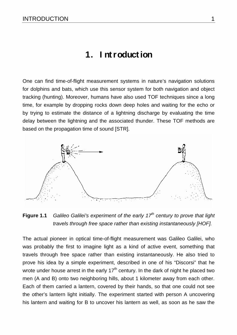
Figure 1.1 Galileo Galilei’s experiment of the early 17th century to prove that light
travels through free space rather than existing instantaneously [HOF].
The actual pioneer in optical time-of-flight measurement was Galileo Galilei, who
was probably the first to imagine light as a kind of active event, something that
travels through free space rather than existing instantaneously. He also tried to
prove his idea by a simple experiment, described in one of his “Discorsi” that he
wrote under house arrest in the early 17th century. In the dark of night he placed two
men (A and B) onto two neighboring hills, about 1 kilometer away from each other.
Each of them carried a lantern, covered by their hands, so that one could not see
the other’s lantern light initially. The experiment started with person A uncovering
his lantern and waiting for B to uncover his lantern as well, as soon as he saw the
2 CHAPTER 1
first lantern’s light (c.f. Figure 1.1). That way Galilei hoped to measure the
propagation time that the light needed to travel from person A to person B and back
to A, a hopeless attempt from today’s point of view, since we know that the light
only needs 6.6 microseconds to travel the distance of 2 kilometers. So much more
remarkable is Galilei’s conclusion from this experience. We know that Galilei was
an excellent engineer: Before carrying out his experiment, he trained the
experimenters to react quickly and measured their reaction times. He found that the
measured speed of light was of the same order of magnitude as the reaction times
that he had previously measured. Therefore, he concluded that either light exists
instantaneously, as physics has taught previously, or that it propagates so
incredibly quickly that it was not possible to measure its speed with the proposed
experiment. A little later, in 1676 it was Roemer who succeeded in measuring the
speed of light by using the departures from predicted eclipse times of a Jupiter
moon, strictly speaking also a TOF experiment.
It was only 200 years later, in1849, that Fizeau was more successful in measuring
the time of flight on earth. He built a more precise, more mature and complicated
experimental setup (illustrated in Figure 1.2) in the suburbs of Paris. Fizeau used a
rotating cogwheel as a mechanical shutter for a focused light beam. This pulsed
beam was projected onto a mirror, located 8633 m away. For an appropriate
rotation speed of the cogwheel the complete light packet, which had been
transmitted by a gap in the wheel was obstructed by a tooth after being reflected by
the distant mirror, so that it could not be seen behind the cogwheel. As the distance
and the shutter rate (rotation period divided by the number of teeth) were known,
Fizeau could calculate the speed of light. With this early TOF experiment he
obtained an astonishingly precise result of 3.153⋅108 m/s.
INTRODUCTION 3
lens
light source
rotatingcogwheel
observer
beam splitter planemirror
lens
lens
lens
Figure 1.2 Fizeau’s experimental setup used to determine the speed of light
in 1849.
Today, the speed of light (c=λ⋅ν) can be determined much more precisely, for
example by the simultaneous measurement of frequency ν and wavelength λ of a
stabilized helium-neon-laser or by the frequency measurement of an
electromagnetic wave in a cavity resonator [BRK]. Since 1983 the speed of light
has been fixed by definition to c=2.99792458⋅108 m/s. With this precise knowledge
of the velocity of light, it is thus possible to modify Galilei’s or Fizeau’s experiments
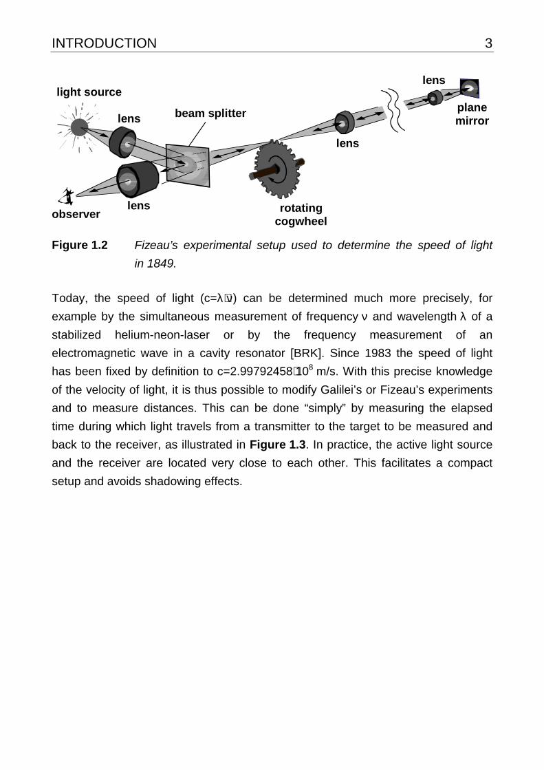
and to measure distances. This can be done “simply” by measuring the elapsed
time during which light travels from a transmitter to the target to be measured and
back to the receiver, as illustrated in Figure 1.3. In practice, the active light source
and the receiver are located very close to each other. This facilitates a compact
setup and avoids shadowing effects.
4 CHAPTER 1
transmitter
3D object
"ns stop watch"
100
80
90
70
6050
40
3020
10
n sn sn sn s
STARTSTOP
detector
DISTANCE
receiver
1m = 6.67ns
Figure 1.3 Basic principle of an (optical) TOF ranging system.
The basic principle can be summarized as follows: A source emits a light pulse and
starts a highly accurate stopwatch. The light pulse travels to the target and back.
Reception of the light pulse by the detector mechanism stops the stopwatch, which
now shows the time of flight of the light pulse. Considering the fact that the light
pulse travels the distance twice (forth and back), a measured time of 6.67 ns
corresponds to a distance of one meter. An essential property of this setup is the
fact that emitter and detector are synchronous. At this point one can recognize a
significant advantage of time-of-flight over a triangulation based ranging system:
The TOF ranging technique does not produce incomplete range data (no shadow
effects) because illumination and observation directions are collinear. It is obvious
that the basic problem of establishing a TOF-ranging system is the realization of a
high accuracy time-measurement mechanism. For a resolution of 1cm, an accuracy
of better than 70 picoseconds is required. The stringent requirements for the
receiver are one reason that, although already in 1903 Hulsmeyer carried out some
experiments with electromagnetic radar, only in 1968 was Koechner one of the first
to introduce an optical TOF ranging system [KOE]. Another problem was the lack of
high power (laser-) light sources. All these TOF ranging systems actually only
measure the distance to a point (1D). In order to gain 3D information, the laser
beam has to be scanned over the scene in two directions. This requires high
accuracy laser scanners, which are mostly bulky and sensitive to vibrations.
INTRODUCTION 5
Propagation time, however, is not the only property of light that is important for this
dissertation. In the early 1900’s another property of light was discovered, the so-
called photoelectric effect. This is the ability of light to interact with matter, either
liberating electrons from a metal plate, for example (external photoelectric effect or
photoemission) or generating electron-hole pairs in semiconductor materials
(internal photoelectric effect or photoconduction). Both effects can be explained by
quantum physics. Albert Einstein as the first to understand the external
photoelectric effect earned the Nobel Price for his explanation.
The discovery of this photoelectric effect opened the doors to electronic image
sensing. Already in 1939 the first electronic imaging devices, so called Orthicons
(later Vidikons), were introduced. They are based on electron tubes and have been
gradually replaced by solid-state cameras with the introduction of the CCD (Charge
Coupled Device) in 1971 [BOY, AME]. This all-solid-state imaging device has
dominated the optoelectronic market for more than two decades now. Only in the
last few years has CMOS (Complementary Metal Oxide Semiconductor) technology
definitely entered the imaging market [FOS]. This technology, mainly driven by the
computer industry, is not only widely available and cheaper than CCD technology,
the classical technology for solid-state imaging devices, but CMOS also makes it
possible to implement additional functionality on-chip. Today’s CMOS sensors can
offer, for example, A/D- conversion and arbitrary access to individual pixels,
enabling the definition of ROI’s (Regions Of Interest) [BLC]. In contrast to CCDs,
CMOS sensors can be operated with low voltages (<5 V) and they consume little
power. Both high resolution and high speed CMOS APS sensors are available and
the image quality is gradually approaching CCD performance [LAX, VOG].
Additionally, a logarithmic response can be realized relatively easily, resulting in an
enormous dynamic range (>130 dB) [VIZ, BLC]. CMOS APS technology is also
used to realize so-called smart pixels, image sensors with special functionality,
such as temporal or local convolution, stereo vision, color vision, motion detection
or velocity measurement, often inspired by visual systems found in nature [MOI].
Until the middle of the 70’s, light barriers were almost exclusively used in machine
vision. Only at the end of the 70’s first video cameras entered the machine vision
market; they were used for object recognition and surveillance. Semiconductor
imagers emerged only in the middle of the 80’s [KAP].

6 CHAPTER 1
With this dissertation, both highly interesting and powerful fields of optoelectronics
are combined for the first time: TOF-range measurement and customized image
sensors with special functionality. We demonstrate an array of monolithically
integrated pixels, where each pixel contains the complete demodulating receiver of
the TOF system. This development represents an enormous improvement for the
field of 3D TOF ranging. Instead of scanning a modulated beam over the scene and
serially taking point distance measurements to combine them into a 3D image, the
range measurements for all observed points in the scene are now performed in
parallel by the individual pixels. The actual correlation process between the
received light and the synchronous reference signal, which is the essential process
to measure the time delay, is performed in each pixel, immediately after the light is
detected. All other electronic components within the following signal processing
chain in the range camera system are more or less uncritical, since the high-speed
demodulation process is already performed within the detection device. This is
another advantage over conventional TOF systems, in which phase drifts of the
system due to temperature variations and aging of critical electrical components are
a serious problem, requiring calibrating reference measurements.
This work is subdivided into seven chapters:
Chapter 2 roughly compares time-of-flight measurement with the other state-of-the-
art measurement principles: optical interferometry and triangulation. The basic
working principles will be discussed, as well as typical advantages and
disadvantages. Application examples will be given. Of the huge variety of operation
principles for TOF ranging, a theoretical description of homodyne TOF-
measurement is derived, with emphasis on the relevant questions for the four-
phase measurement technique used in this work. In this homodyne operation
mode, the phase delay (rather than the time delay) of a modulated light wave is
measured. It is shown that by demodulating the incoming modulated light, the
modulation signal’s amplitude and phase can be extracted. In particular, the
influence of system non-linearities, the integrative nature of natural sampling, the
choice of modulation signal, the total integration time and aliasing effects are
discussed in detail. It is shown that the four phase measurement technique is
insensitive to 1st and 2nd order non-linearities and to even harmonics, assuming
properly chosen integration times for the sampling points.
INTRODUCTION 7
Chapter 3 gives a short overview and comparison of CCD and CMOS image
sensors. It is pointed out that we have to distinguish between CCD principle and
CCD technology, since the latter is only a dedicated, optimized process for large
area CCD imagers. The CCD principle can also be realized in (slightly modified)
CMOS processes. We have used a 2.0µm CMOS/CCD process for all monolithical
implementations presented in this work. This process makes it possible to realize
CCDs with a charge transfer efficiency (CTE) between 96 % and 99.6 % at 20 MHz
transport frequency, depending on the number of electrons to be transported (96 %:
10,000 e-, 99.6 %: 1’000’000 e-). Dedicated CCD processes reach typical CTE
values of 99.9998 % and better. In spite of the inferior CTE performance compared
with a CCD process, the availability of the CCD principle offers enormous
capabilities, such as virtually noise-free single electron level signal addition or fast
signal sampling. For these useful properties, which have not been demonstrated
with any transistor-based CMOS circuitry so far, a fair CCD performance is
sufficient. This is of essential importance for an economic product development,
since (1) CMOS processes are available as Multi-Project-Wafers (MPWs) for
affordable prototyping and (2) additional functionality such as A/D conversion or
any kind of signal processing can easily be implemented on chip. The advantages
of both CCD and CMOS will be pointed out. The chapter is completed by an
overview of those characteristics of silicon images sensors in general, that are of
special interest for the underlying TOF-application: spectral and temporal response,
optical fill factor and noise sources.
Since optical TOF ranging uses active illumination, an optical power budget is very
important. In Chapter 4 we show the relations between the optical power of the
light source, the number of electrons generated in a pixel of the imager and the
resulting output voltage swing. This budget is influenced by the power and
wavelength of the light source, the color, reflectivity and distance of the illuminated
and imaged surface, the choice of optics of the camera as well as the quantum
efficiency, integration time and internal electrical amplification of the image sensor.
Also an estimation of the resolution limit is carried out. For this calculation, the
quantum noise is mainly considered as a final theoretical limitation. Together with
the power budget, the range accuracy can then be calculated depending on the
nature of the target and the technical properties of the TOF-camera.
8 CHAPTER 1
The key element of the new 3D-range camera, the demodulation-pixel imager, is
introduced in Chapter 5. We show that a phase delay can be measured simply by
electrooptically sampling the received modulated light. After the definition and an
overview of the required properties of demodulation pixels, several implemented
solutions will be introduced and their working principle will be described. The pixel
layout with the best performance will be treated in more detail. Characterizing
measurements will show its excellent performance even at 20 MHz modulation
frequency and the influence of control signal amplitude, modulation frequency and
wavelength and optical power of the modulated light source on both measured
contrast and time accuracy. For an optical power of only 600 fW per pixel, where
only one electron is generated, statistically speaking, every 16th modulation period
(equivalent photocurrent: 200 fA), the measured time resolution is better than 300
picoseconds (modulation frequency: 20 MHz, integration time 4·12.5 ms=50 ms;
20 Hz frame rate). This small amount of received radiation power is therefore
sufficient for a distance resolution of better than 5 cm, i.e. 0.67 % of the
unambiguous distance range of 7.5 meters. A comparison of the measured results
with the theoretical limitations deduced in Chapter 4 shows an excellent fit.
Based on this pixel structure, two sensor arrays, a 108-pixel line and a 64x25-pixel
imager, have been implemented and build into two separate range camera
systems. In Chapter 6 we describe both, the sensor implementations and the
complete camera systems in detail. Finally, the first real distance measurements
carried out with these camera systems are presented. Again, the accuracy
achieved agrees reasonably well with the theory. As the demodulation sensor not
only delivers the phase information in every pixel but at the same time modulation
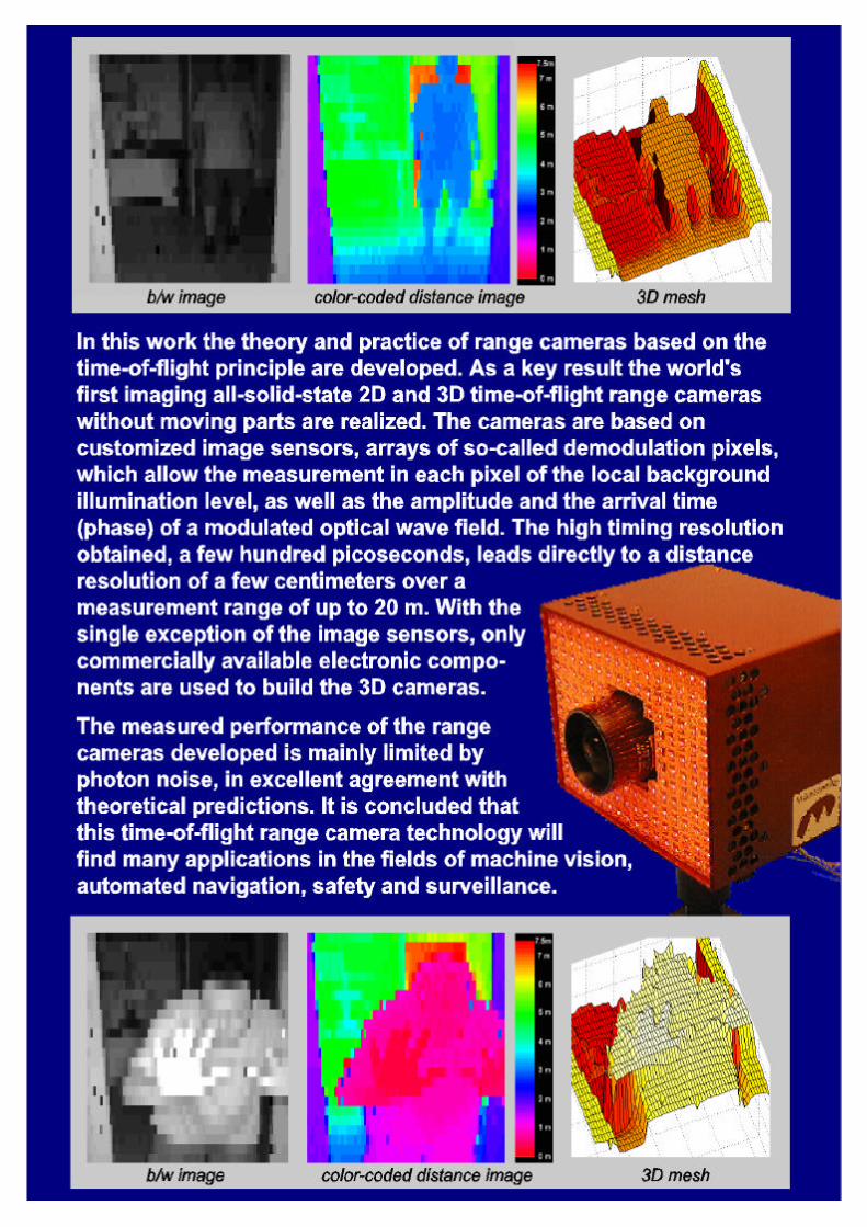
amplitude and background information, the 3D-camera offers both 3D images and
conventional 2D gray level images.
A brief summary and an assessment of future developments and possible
improvements close this work.

OPTICAL TOF RANGE MEASUREMENT 9
2. Optical TOF range measurement
The basic principles of optical range measurement techniques (1) triangulation, (2)
interferometry and (3) time-of-flight are introduced in this chapter. All these
techniques mostly work with light, i.e. electromagnetic radiation fields in the
wavelength range of 400-1000 nanometers (visible and NIR spectrum). We present
a rough description of the basic working principles. The advantages and
disadvantages of each principle are discussed and some examples are also given.
More detailed and broader overviews over optical ranging principles can be found
in the references [KAP], [BES], [ENG], [EN2], [SC1]. Figure 2.1 shows the family
tree of contactless 3D shape measurement techniques.
Contactless 3D shape measurements
Microwaveλ = 3 - 30 mm(10 - 100 GHz)
Light waveλ = 0.5 - 1 µm
(300 - 600 THz)
Ultrasonic waveλ = 0.1 - 1 mm(0.3 - 3 MHz)
Triangulation
depth detection by means of geometrical angle measurement
Interferometry
depth detection by means of optical coherent time-of-flight measurement
Time-of-flight (TOF)
depth detection by means of optical modulation time-of-flight measurement
Figure 2.1 Family tree of contactless 3D shape measurement [SC1].
Since TOF measurement is the underlying principle of this work, it is discussed in
more detail. The first part of this chapter is closed by a discussion and a
comparison of the different ranging techniques. It should be mentioned that also
microwave (λ=3–30 mm) and ultrasound (λ=0.1-1 mm) techniques have their
application-specific advantages. However, they are not included in this comparison.
Due to diffraction limitations, both techniques are not suited for range
measurements with high angular resolution, at an acceptable size of the
10 CHAPTER 2 measurement system. They find their applications in differential GPS or synthetic
aperture radar (SAR) [SC1].
Out of a large variety of modulation techniques for TOF, homodyne phase-shift
modulation is chosen for the operation of the ranging sensors introduced in this
work. Therefore, in the second part of this chapter, the equations will be derived for
the four-phase realization of homodyne modulation. We show that sampling is
always also a correlation process and analyze theoretically the influences of
sampling interval, modulation signal and integration time on the result of
demodulation and the system performance. Aliasing effects are discussed and it is
shown that 1st and 2nd order non-linearities and even harmonics have no influence
on the four-phase algorithm.
OPTICAL TOF RANGE MEASUREMENT 11 2.1 Overview of range measurement techniques
2.1.1 Triangulation
This ranging technique has been known and used by nature for millions of years. It
is, in the form of stereo-vision together with the depth-of-focus system (which so to
speak also belongs to triangulation systems), the basis for human depth perception.
Triangulation is a geometrical approach, where the target is one point of a triangle
whose two remaining points are known parts of the measurement system. The
distance of the target can then be determined by measuring the triangle’s angles or
the triangulation base. Literature distinguishes passive and active triangulation
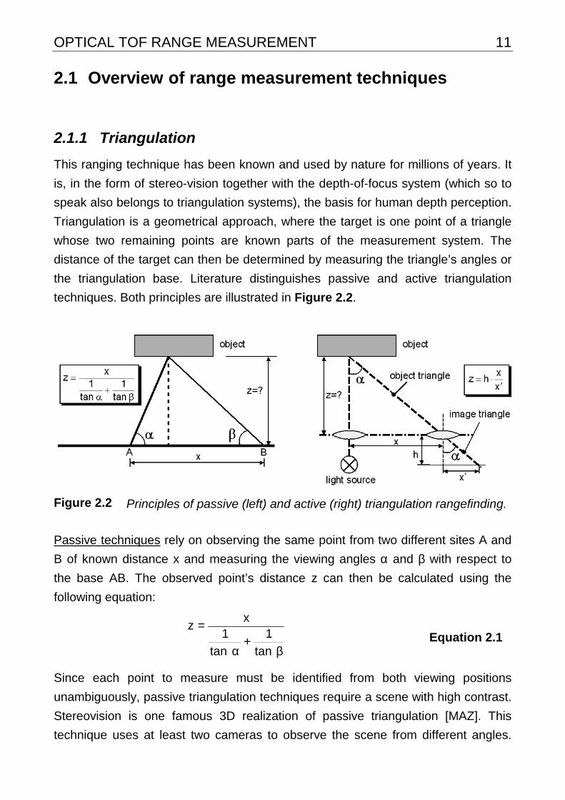
techniques. Both principles are illustrated in Figure 2.2.
Figure 2.2 Principles of passive (left) and active (right) triangulation rangefinding.
Passive techniques rely on observing the same point from two different sites A and
B of known distance x and measuring the viewing angles α and β with respect to
the base AB. The observed point’s distance z can then be calculated using the
following equation:
β+
α
=
tan
1
tan
1x
z Equation 2.1
Since each point to measure must be identified from both viewing positions
unambiguously, passive triangulation techniques require a scene with high contrast.
Stereovision is one famous 3D realization of passive triangulation [MAZ]. This
technique uses at least two cameras to observe the scene from different angles.
12 CHAPTER 2 Using 2D-correlation, typical object features are found and compared in both
images. From the position of each feature’s centroid in both separate images, the
angles α and β can be deduced and the distance can be calculated with
Equation 2.1, assuming that the distance of the cameras with respect to each
other, as well as their orientation are known. The computational effort must not be
underestimated. Shadowing effects are also typical problems with which all
triangulation systems have to cope. Stereovision works pretty well for certain
defined scenes, preferably chosen with rich contrast and relatively flat objects. For
typical industrial scenes, however, it is often not suitable. Though the shadowing
problem can be minimized by enlarging the number of cameras and realizing
“multiple viewpoint triangulation systems”, this improvement has to be paid for by
an enormous increase in computation. Nevertheless, shadowing and the need for
significant contrast in the targeted scene remain a problem. Additionally, cost and
overall system size, one major drawback of triangulation systems anyhow, increase
with the number of cameras. Another famous member of passive triangulation
systems is the theodolite.
Active triangulation, as illustrated in Figure 2.2, uses a light source to project a
point (in the simplest case) to the scene, which is observed by a position sensitive
detector. Rather than measuring angles directly, active triangulation is based on the
similarity of triangles, the object triangle and the image triangle, which is fully
defined by the optical axis of the imaging device, the focal length h of the system
and the position of the point projection x’ on the detector. With knowledge of the
displacement x of the light source from the imaging device, the distance z of the
target can be determined:
x
xhz
′⋅= Equation 2.2
For a good distance resolution δz, small absolute distances z, a large triangulation
base x and a good local detector resolution δx’ are required. δz estimates to:
xx
z
h
1z
2′δ⋅⋅=δ Equation 2.3
With laser point projection, 3D information can only be gained by scanning the laser
point over the scene and thus sequentially acquiring a cloud of range points [RIX,
BER]. A faster approach is to project a line (or light sheet) onto the 3D scene. By
replacing the position sensitive line sensor by an imaging array, a 2D distance
OPTICAL TOF RANGE MEASUREMENT 13 profile can then be measured with one shot, and for 3D data the scan only needs to
be performed in one direction (light sheet triangulation). In industrial inspection
applications, such a 1D scan is often available free of cost, since the objects to
measure are moving anyway, for example on an assembly-line. [KRA] presents
such a scanning 3D camera working with active light sheet triangulation and
delivering 50 depth images per second in CCIR video format.
Further advanced techniques even use 2D structured light illumination and 2D
imaging to perform 3D triangulation measurements without scanning. The most
important members of this structured light group are phase shifting projected fringe,
Gray code approach [BRE], phase shifting moiré [DOR], coded binary patterns,
random texture [BES] or color-coded light. They typically use LCD (Liquid Crystal
Display) projectors for the projection of the structured patterns.
Triangulation systems are available for applications from mm-range (depth of focus)
to 100km range (photogrammetry). Their main drawback is that for a good
resolution they have to be large in size, since they need a large triangulation base.
On the other hand, the larger this triangulation base, the more they are restricted by
shadowing effects. Also, 3D triangulation systems are relatively expensive since
they require fast LCD projectors (only active systems) as well as large
computational power.
2.1.2 Interferometry
Interferometry is described by the superposition of two monochromatic waves of
frequency ν, amplitude U1 and U2 and phase ϕ1 and ϕ2, respectively, resulting in
another monochromatic wave of the same frequency ν, but with different phase and
different amplitude [SAL]. In the easiest interferometer setup, the Michelson
interferometer, illustrated in Figure 2.3, a laser beam (monochromatic and
coherent) is split into two rays by a beam splitter. One ray is projected to a mirror of
constant displacement x1 (reference path) whereas the other beam is targeted on
the object of variable distance x2 (measurement path). Both beams are reflected
back to the beam splitter, which projects them onto an integrating detector.

14 CHAPTER 2
Figure 2.3 Working principle of Michelson interferometer
With the reference wave U1 and the object wave U2 defined as
( )
( )λ
⋅⋅π
λ⋅⋅π
⋅=
⋅=
2
1
x22j
22
x22j
11
eIU
eIU Equation 2.4
(I1 and I2 are the optical intensities) we obtain the interference equation
( )
λ⋅−⋅⋅π⋅⋅++= 12
2121x2x22
cosII2III Equation 2.5
Note that we have to consider the double path lengths 2·x1 and 2·x2 respectively
because the light waves travel the paths twice, forth and back. For equal reference
and measurement path x1 and x2, as well as for path differences of exact multiples
of the light’s half wavelength λ/2, the intensity on the detector reaches a maximum.
This case is denoted as constructive interference. For a path difference λ/4 or
n⋅λ/2 + λ/4, the intensity tends to a minimum: destructive interference.
A movement of the object away from the system (or towards the system) results in
an intensity peak of the interferogram (constructive interference) each time the
object has moved by a multiple of the laser’s half wavelength. By recording and
counting the number of minimum-maximum transitions in the interference pattern
over time, when the object moves, the distance of movement can be incrementally
determined at an accuracy of the light’s wavelength or even better [CRE].
Interferometry therefore uses the light’s built-in scale, its wavelength, for performing

OPTICAL TOF RANGE MEASUREMENT 15 highly accurate relative distance measurements. This technique can be equivalently
interpreted as a time-of-flight principle, since the runtime difference between the
reference and measurement path is evaluated.
Several other interferometer setups can be found, for example in [SAL] or [HEC].
The principal drawback of classical interferometers is that absolute distance
measurements are not possible and the unambiguous distance range is as low as
half the wavelength. Enhanced approaches overcome this restriction. One nice
example is Multiple-wavelength interferometry, where two very closely spaced
wavelengths are used at the same time. That way beat frequencies down to GHz or
even MHz range are synthetically generated, enabling absolute measurements
over several tens of centimeters at λ/100 resolution [ZIM, SC1]. Especially
important for high sensitivity 3D deformation measurements is the electronic
speckle pattern interferometry (ESPI), where a reference wave front interferes with
the speckle pattern reflected by the investigated object. With a conventional CCD
camera the speckle interferogram, carrying information of the object deformation,
can then be acquired. Like conventional interferometers, ESPI can also be
improved in sensitivity and measurement range by the multiple-wavelength
technique. [ENG]
Another way to enlarge the measurement range is to use light sources of low
coherence length. Such interferometers (white-light interferometry or low-coherence
interferometry [BOU]) make use of the fact that only coherent light shows
interference effects. If the optical path difference between the measurement and
reference paths is higher than the coherence length of the light, no interference
effects appear. For a path difference of the order of magnitude of the coherence
length, however, interference takes place. The strength of interference, depends on
the path difference between the reference and object beams, and thus absolute
distances can be measured.
Interferometry finds its applications predominantly for highly accurate
measurements (λ/100 to λ/1000) over small distances ranging from micrometers to
several centimeters.

16 CHAPTER 2 2.1.3 Time-of-flight
Similarly to interferometry, we can measure an absolute distance if we manage to
measure the absolute time that a light pulse needs to travel from a target to a
reference point, the detector. This indirect distance measurement is possible since
we know the speed of light very precisely: c = 3⋅108 m/s = 2⋅150 m/µs =
2⋅0.15 m/ns = 2⋅0.15 mm/ps [BRK, BRR]. In practice, the active light source and the
receiver are located very closely to each other. This facilitates a compact setup and
avoids shadowing effects. The basic principle of a TOF-ranging system is illustrated
in Figure 1.3. A source emits a light pulse and starts a high accuracy stopwatch in
the detector. The light pulse travels to the target and back. Reception of the light
pulse by the detector mechanism stops the time measurement and the stopwatch
now shows the time of flight of the light pulse. Considering the fact that the light
pulse travels the path twice (forth and back) a measured time of 6.67 ns
corresponds to a distance of 1 m and a time accuracy of better than seven
picoseconds is required for a distance resolution of 1 mm. An essential property of
this setup is the fact that emitter and detector are operated synchronously. At this
point one can already recognize a significant advantage of time-of-flight over a
triangulation system: The TOF ranging technique does not produce incomplete
range data (no shadow effects) because illumination and observation directions can
be collinear.
Also, the basic problem of establishing a TOF-ranging system is obvious here: the
realization of a high accuracy time measurement. In the following subchapters
different operation modes and the associated components (light source, modulator,
demodulator, detector) for TOF applications are introduced.
I. MODULATION SIGNALS
Generally, TOF ranging systems use pulsed modulation [MOR] or continuous (CW)
modulation [BEH] of the light source; combinations of both are also possible (e.g.
pseudo-noise modulation). Both modulation principles have their specific
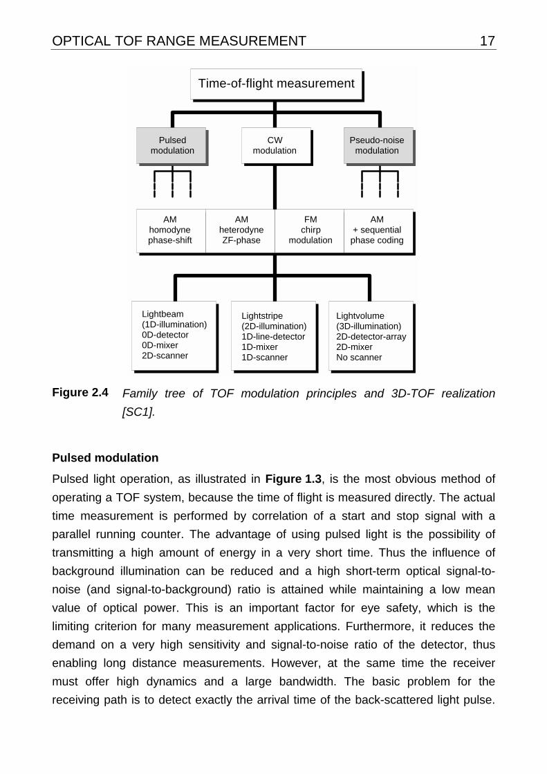
advantages and disadvantages, which are treated in the following. Figure 2.4 gives
an overview over the different types of modulation signals available for TOF
systems.
OPTICAL TOF RANGE MEASUREMENT 17
Time-of-flight measurement
Pulsedmodulation
CWmodulation
Pseudo-noisemodulation
AMhomodynephase-shift
AMheterodyneZF-phase
FMchirp
modulation
AM + sequentialphase coding
Lightbeam(1D-illumination)0D-detector0D-mixer2D-scanner
Lightstripe(2D-illumination)1D-line-detector1D-mixer1D-scanner
Lightvolume(3D-illumination)2D-detector-array2D-mixerNo scanner
Figure 2.4 Family tree of TOF modulation principles and 3D-TOF realization
[SC1].
Pulsed modulation
Pulsed light operation, as illustrated in Figure 1.3, is the most obvious method of
operating a TOF system, because the time of flight is measured directly. The actual
time measurement is performed by correlation of a start and stop signal with a
parallel running counter. The advantage of using pulsed light is the possibility of
transmitting a high amount of energy in a very short time. Thus the influence of
background illumination can be reduced and a high short-term optical signal-to-
noise (and signal-to-background) ratio is attained while maintaining a low mean
value of optical power. This is an important factor for eye safety, which is the
limiting criterion for many measurement applications. Furthermore, it reduces the
demand on a very high sensitivity and signal-to-noise ratio of the detector, thus
enabling long distance measurements. However, at the same time the receiver
must offer high dynamics and a large bandwidth. The basic problem for the
receiving path is to detect exactly the arrival time of the back-scattered light pulse.
18 CHAPTER 2 This is because (1) the optical threshold is not a fixed value but changes with
background and distance of the object, and (2) atmospheric attenuation leads to
dispersion of the light pulse and flattens the slope of the received pulse. Also, it is
tricky to produce very short light pulses with fast rise and fall times, which are
necessary to assure an accurate detection of the incoming light pulse. Current
lasers or laser diodes, the only optical elements offering the required short pulse
widths at sufficiently high optical power, still suffer from relatively low repetition
rates for the pulses, which typically are in the range of some 10 kHz. Such low
repetition rates drastically restrict the frame rate for TOF scanners.
Nevertheless, due to the advantages gained concerning signal-to-background ratio,
most of today’s TOF rangefinders are operated with pulsed modulation. [LEI, RIG]
Continuous wave (CW) modulation
CW-modulation offers the possibility of using alternative modulation-, demodulation-
and detection-mechanisms. Compared to pulsed modulation a larger variety of light
sources is available for this mode of operation because extremely fast rise and fall
times are not required. Different shapes of signals are possible; sinusoidal waves or
square waves are only some examples. For CW-modulation generally the phase
difference between sent and received signals is measured, rather than directly
measuring a light pulse’s turn-around time. As the modulation frequency is known,
this measured phase directly corresponds to the time of flight, the quantity of
interest.
The use of several modulation frequencies is known as heterodyne operation or
frequency shifting [SC3]. Heterodyne mixing especially offers the powerful
possibility of synthetically generating beat frequencies. Thus the unambiguous
distance range is increased while maintaining absolute accuracy. However, this
requires relatively high bandwidth and linearity for both transmitting and receiving
path.
In this work we mainly whish to demonstrate the possibility of realizing 3D-TOF with
custom photoASICs. Rather than examining all possible modulation modes, we
focus on homodyne operation (phase shifting technique), as discussed in more
detail in Chapter 2.2. The homodyne operation works with one single frequency
and does not necessarily require a large bandwidth.
OPTICAL TOF RANGE MEASUREMENT 19 Additionally, a large variety of intelligent CW modulation techniques is available. It
is worth mentioning pseudo-random modulation and chirping (continuous frequency
modulation) [XU]. Pseudo-random modulation, where pseudo noise words (PN
modulation) are continuously repeated, offers the advantage of a very high peak in
the autocorrelation function. This technique, originally developed for communication
technology, is therefore very noise-robust [SC2].
A combination of both CW modulation and pulsed modulation would be ideal,
combining their specific advantages of (1) better optical signal-to-background ratio
than available from pure CW-modulation, (2) increased eye safety due to a low
mean value of optical power and (3) larger freedom in choosing modulation signals
and components. Combination in this content means, for example, a “pulsed sine”
operation, i.e. a sequence of 1 ms high power sine modulation followed by 9 ms of
optical dead time. This dead time can be used for example for post processing
tasks.
II. COMPONENTS
In the following, the necessary components for TOF systems will be described and
associated with the corresponding modulation technique.
Modulated light sources and electrooptical modulators
The emitted light can be modulated in several ways. The use of LEDs or lasers
allows direct modulation of the light source by controlling the electrical current.
Since the light sent does not have to be coherent or monochromatic, other light
sources are possible, in combination with additional large aperture optical
modulators such as Kerr cells [HEC], Pockels cells [HEC, SC3], mechanical
shutters or liquid crystal shutters. Pulsed operation with fast rise and fall times is
only possible with directly controlled laser sources that allow pulses of less than ten
femtoseconds [SUT]. The different light sources and modulators can be
characterized in terms of light intensity, cut-off frequency, linearity, wavelength,
modulation depth (the ratio of signal amplitude to signal offset), eye safety
properties, size and price.
LEDs are relatively inexpensive. They can be modulated up to some 100 MHz with
a 100% modulation depth and a very high linearity. They are available for a wide
20 CHAPTER 2 range of wavelengths from blue (400 nm) to the near infrared (1200 nm) with an
optical power of up to several milliwatts. Lasers, even laser diodes, are much more
expensive than LEDs and are often larger. However, they offer more optical power
and are suited for operation up to some GHz, also at a wide range of wavelengths
[SAL]. Practically, lasers and laser diodes are the only light sources suitable for
pulsed TOF operation. All other light sources introduced here are actually used for
CW modulated light, due to the reduced bandwidth requirements.
Kerr cells are based on the quadratic electro-optic effect, where the polarization of
a polarized beam is rotated depending on the applied voltage. Together with a
polarizer and a modulated control voltage of the cell, a polarized incoming beam
can be modulated in intensity. Kerr cells can be used as modulators up to 10 GHz
but voltages as high as 30 kV must be switched at this speed [HEC]. Pockels cells,
making use of the linear electro-optic effect (pockels effect), work very similarly and
also require polarized light for operation. Their cut-off frequency of more than
25 GHz is even higher than that of Kerr cells. The driving voltage requirements are
a factor of 10 lower than for an equivalent Kerr cell. However, the Pockels cell still
requires some kilovolts to switch from transparent to opaque mode. Therefore, the
practical cut-off frequency, which is limited by the cell’s capacitance, reaches only
several hundred MHz [HEC, SAL, XU].
Liquid crystal shutters are limited to some kHz of modulation frequency and are
therefore not suited for high-resolution measurement applications in the 10 meter
range [SAL]. An interesting alternative, however, might be the realization of a
mechanical shutter. Miniaturized air turbines with a rotation speed of 427’000 rpm
have been reported [SLO]. If one manages to rotate a light grating disc with such
an air turbine, shutter frequencies as high as 1 MHz might become possible. For
example, a disc of 10cm diameter and a slot width of 1 mm at the edge of the disc
would contain about 150 slots. Such a disc would offer a 1x1 mm2 shutter aperture
while allowing 1 MHz shutter frequency (=150*427000(1/min)/60(s/min)).
Detectors and Demodulation
The easiest and most straightforward way of realizing a TOF-receiver is to use any
fast and sensitive electrooptical sensor as a detector. The time of flight can then be
determined as follows: a linear analog ramp (or a fast digital counter) is started
synchronously with the transmission of a laser pulse. Once the laser pulse reaches
the detector the rise of the ramp is stopped. The resulting amplitude is then
OPTICAL TOF RANGE MEASUREMENT 21 proportional to the time of flight. The difficulty of this detection mechanism is the
definition of a trigger level for the detector, because the amplitude of the received
light strongly depends on the distance, background and the surface to measure.
For 1D-TOF ranging systems, high dynamic, high sensitivity PIN photo diodes or
APDs (avalanche photo diodes) are used. PIN photo diodes have a very fast
response. Typical cut-off frequencies are 10 GHz and beyond. After the fast
detection, the modulated light, now converted to an electrical signal, is electrically
demodulated (using sophisticated special purpose ICs) leading to the desired
phase difference between transmitter and receiver. This electrical demodulation
often suffers from temperature drifts of the electric components involved. Therefore,
regular reference measurements and calibration are necessary to ensure
reproducible measurements. APDs and photomultiplier tubes [PAR] can be
modulated in their sensitivity, enabling a direct demodulation or mixing of the
incoming light. Today, TOF rangefinders and TOF laser scanners are available with
mm accuracy for cooperative and several cm resolution for non-cooperative targets
over a distance of some 10 up to 100 meters and more [LEI, KAI].
All these components only allow a 1D measurement, i.e. the distance measurement
of one point in the 3D scene. The operation of many such receivers in parallel
appears to be impractical due to large size and enormous demand on additional
electronics. Therefore, 2D depth profiles or 3D depth images can only be obtained
from such 0D detectors by scanning the light beam over the observed surface.
This, however, requires time, because every point has to be measured serially. It
also requires mechanical scanners of very high precision. Those scanners are
bulky, expensive, and sensitive to vibrations.
III. 3D TOF RANGING
Instead of scanning a laser beam and serially acquiring the range data point-wise,
we can illuminate the entire scene with a modulated light surface in order to
perform a 3D measurement, as illustrated in Figure 2.5. This, however,
necessitates the use of a 2D-electrooptical demodulator and detector to measure
the distances of some hundreds or thousands of points of the observed scene in
parallel.
The 2D detection itself can be performed with CCDs or (active) photodiode arrays,
so called active pixel sensors (APS). However, in contrast to discrete photodiodes,
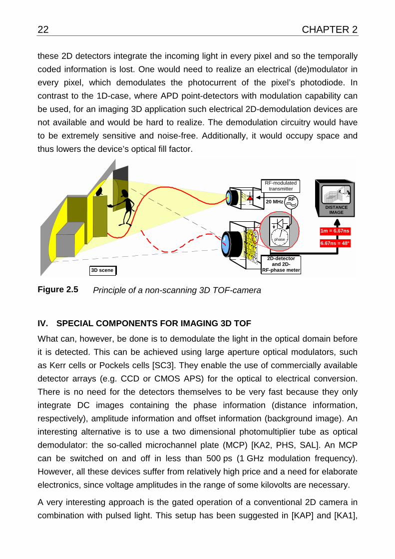
22 CHAPTER 2 these 2D detectors integrate the incoming light in every pixel and so the temporally
coded information is lost. One would need to realize an electrical (de)modulator in
every pixel, which demodulates the photocurrent of the pixel’s photodiode. In
contrast to the 1D-case, where APD point-detectors with modulation capability can
be used, for an imaging 3D application such electrical 2D-demodulation devices are
not available and would be hard to realize. The demodulation circuitry would have
to be extremely sensitive and noise-free. Additionally, it would occupy space and
thus lowers the device’s optical fill factor.
2D-detectorand 2D-
RF-phase meter3D scene
DISTANCEIMAGE
RF-modulatedtransmitter
RF
6.67ns = 48°
1m = 6.67ns
20 MHz
phase
Figure 2.5 Principle of a non-scanning 3D TOF-camera
IV. SPECIAL COMPONENTS FOR IMAGING 3D TOF
What can, however, be done is to demodulate the light in the optical domain before
it is detected. This can be achieved using large aperture optical modulators, such
as Kerr cells or Pockels cells [SC3]. They enable the use of commercially available
detector arrays (e.g. CCD or CMOS APS) for the optical to electrical conversion.
There is no need for the detectors themselves to be very fast because they only
integrate DC images containing the phase information (distance information,
respectively), amplitude information and offset information (background image). An
interesting alternative is to use a two dimensional photomultiplier tube as optical
demodulator: the so-called microchannel plate (MCP) [KA2, PHS, SAL]. An MCP
can be switched on and off in less than 500 ps (1 GHz modulation frequency).
However, all these devices suffer from relatively high price and a need for elaborate
electronics, since voltage amplitudes in the range of some kilovolts are necessary.
A very interesting approach is the gated operation of a conventional 2D camera in
combination with pulsed light. This setup has been suggested in [KAP] and [KA1],
OPTICAL TOF RANGE MEASUREMENT 23 where an optical modulator works as an electrooptical shutter with varying
sensitivity over time. A similar realization, making use of the built-in electronic
shutter of a conventional CCD camera, rather than an additional optical modulator,
is described in [DAS]. This system works as follows: A light pulse of some tens of
nanoseconds is transmitted by a laser and it synchronously starts the integration of
a standard CCD camera. With the electrical shutter mechanism of the CCD
camera, only a very short period of time (also some tens of nanoseconds) is
integrated. Thus, depending on the distance of the targets, only a fraction of the
light pulse arrives before the integration stops. Performing two calibration
measurements, one without laser illumination and one with non-pulsed, continuous
laser illumination, enables distance calculation. However, compared to the total
power consumption of nearly 200 Watts, the distance resolution of ± 20 cm for non
cooperative targets in a 10 m range at 7 Hz frame rate is relatively poor. The
reason for this low performance is that no repetitive integration is possible; the CCD
has to be read out after every short time integration. This leads to a poor signal-to-
noise ratio of this realization that can only be compensated by very high optical
power of the laser. The power of laser sources, on the other hand, is limited by eye
safety regulations.
The restriction of conventional CCDs only allowing one short-time integration, as
described above, requires innovative, smarter 2D demodulation arrays realized as
customized PhotoASICs. The first such device, realized in CCD technology, was,
however, not intended to be used in an optical ranging system but for a 2D-
polarimeter [POW]. For simplified 3D TOF measurement without mechanical
scanners, the lock-in CCD sensor was invented [SP1-SP4]. Based on these lock-in
structures, we present arrays of improved demodulation pixels in Chapter 5. In
these pixels, CCD gates are arranged such that light generated charge carriers
under the photo gate can be moved to different storage sites. This allows fast
sampling of incoming light, enabling the measurement of phase and amplitude of
the modulated light, as described later in Section 2.2. A related architecture, which
is operated with modified sinusoidal control signals, is the photonic mixer device
(PMD) [SC2, XU]. This device has a modified differential amplifier in every pixel,
which integrates the sum and the difference of two demodulation currents,
demodulated with 180° phase difference.
24 CHAPTER 2 With such demodulation pixels, 3D cameras can be realized without any
mechanically moving parts and with no need for expensive and elaborate large
aperture electrooptical modulators. These 3D cameras of the future, presented in
Chapter 6, are both inexpensive, small, relatively low-power (compared to existing
TOF-systems) and vibration robust.
2.1.4 Discussion
In the previous sections we have introduced the three basic optical measurement
principles: triangulation, interferometry and time-of-flight. To measure always
means to correlate. Even the trivial process of measuring a distance with a folding
rule is a correlation process, where the object to be measured is correlated with the
scale of the folding rule. In this context we might describe triangulation for example
as a local correlation of imaged projected stripe patterns with the pixel pattern on
the image sensor. Interferometry is a temporal correlation or optical interference
between the object wave and the reference wave and time-of-flight is the temporal
correlation of the received modulation signal (carried by light) with the electrical
reference signal. Figure 2.6 shows a comparison of available implementations in
terms of distance range and resolution.

OPTICAL TOF RANGE MEASUREMENT 25
Distance z
Me
asu
rem
en
t u
nce
rta
inty
δ z z
1mm 1cm 10cm 1m 10m 100m 1km 10km
10 -1
10 -2
10 -3
10 -4
10 -5
10 -6
10 -7
10 -8
Time-of-flight m
easurement
Triangulation
Interferometry
Projected fringe
Theodolite
Depth of focus
Photogrammetry
White-light IFSpeckle IF
Multi λ IF
Figure 2.6 Performance map of conventional optical 3D systems [SC1].
Absolutely independent of the progress and steady improvements in rangefinders,
we experience a continuously improving and rapidly growing field of industry:
microelectronics. For sure, each of the optical ranging methods introduced before
has profited in its own way from the ongoing miniaturization in microelectronics.
However, while triangulation and interferometry saw more cost-effective
implementations, their measurement accuracy was not substantially affected. In the
case of triangulation, the measurement range and precision is critically determined
by the triangulation baseline. Obviously, miniaturization of the complete system
leads to a reduced triangulation baseline and therefore to reduced accuracy. The
precision in interferometry is basically given by the wavelength of the employed
coherent light source, a parameter that cannot be influenced greatly. The situation
is completely different for time-of-flight (TOF) range imaging techniques. They have
not only become cheaper, smaller and simpler to realize but their measurement
accuracy is also increasing steadily. This is because, generally speaking, with
decreasing minimum feature size, devices become faster and hence, a better time
resolution is possible. Therefore, we believe that the time-of-flight measurement
principle will be used in more and more future applications.
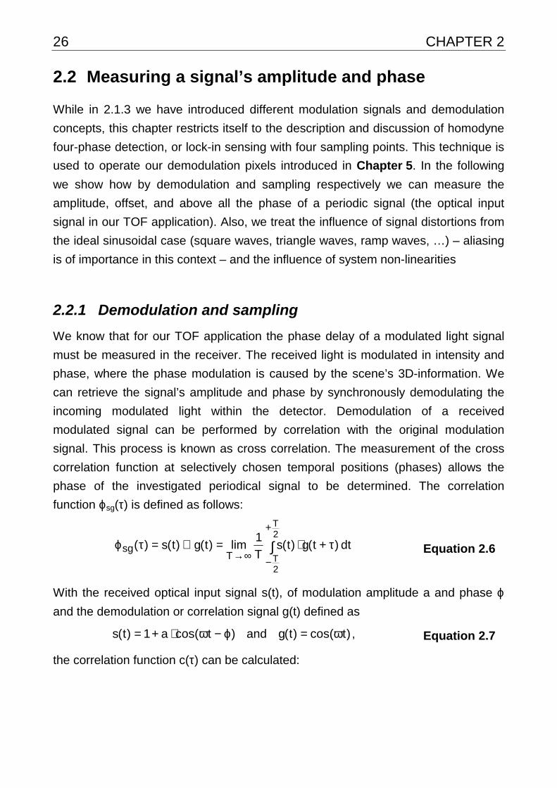
26 CHAPTER 2 2.2 Measuring a signal’s amplitude and phase
While in 2.1.3 we have introduced different modulation signals and demodulation
concepts, this chapter restricts itself to the description and discussion of homodyne
four-phase detection, or lock-in sensing with four sampling points. This technique is
used to operate our demodulation pixels introduced in Chapter 5. In the following
we show how by demodulation and sampling respectively we can measure the
amplitude, offset, and above all the phase of a periodic signal (the optical input
signal in our TOF application). Also, we treat the influence of signal distortions from
the ideal sinusoidal case (square waves, triangle waves, ramp waves, …) – aliasing
is of importance in this context – and the influence of system non-linearities
2.2.1 Demodulation and sampling
We know that for our TOF application the phase delay of a modulated light signal
must be measured in the receiver. The received light is modulated in intensity and
phase, where the phase modulation is caused by the scene’s 3D-information. We
can retrieve the signal’s amplitude and phase by synchronously demodulating the
incoming modulated light within the detector. Demodulation of a received
modulated signal can be performed by correlation with the original modulation
signal. This process is known as cross correlation. The measurement of the cross
correlation function at selectively chosen temporal positions (phases) allows the
phase of the investigated periodical signal to be determined. The correlation
function ϕsg(τ) is defined as follows:
∫+
−∞→
τ+⋅=⊗=τϕ2T
2T
dt )t(g)t(sT
1lim)t(g)t(s)(
Tsg Equation 2.6
With the received optical input signal s(t), of modulation amplitude a and phase ϕ
and the demodulation or correlation signal g(t) defined as
)tcos(a1)t(s ϕ−ϖ⋅+= and )tcos()t(g ϖ= , Equation 2.7
the correlation function c(τ) can be calculated:
OPTICAL TOF RANGE MEASUREMENT 27
[ ] [ ]
[ ] [ ]
( )ϖτ+ϕ⋅=
ϖτ+ϖ⋅ϕ−ϖ⋅+=
ϖτ⊗ϕ−ϖτ⋅+=τϕ=τ
∫+
−∞→
cos2
a
dt )tcos()tcos(a1'T
1lim
)cos()cos(a1)()(c
2'T
2'T'T
sg
Equation 2.8
We evaluate this function for different phases ϖτ. Choosing ϖτ0=0°, ϖτ1=90°,
ϖτ2=180° and ϖτ3=270° allows us to recalculate the phase ϕ and amplitude a of the
received optical signal s(t). Considering that the received signal is mostly
superimposed on a background image, we must add an offset K to the correlation
function to obtain the real measured values C(τ)=c(τ)+K:
( )
( )
( )
( ) Ksin2
aK)(c)(C
Kcos2
aK)(c)(C
Ksin2
aK)(c)(C
Kcos2
aK)(c)(C
33
22
11
00
+ϕ⋅=+τ=τ
+ϕ⋅−=+τ=τ
+ϕ⋅−=+τ=τ
+ϕ⋅=+τ=τ
Equation 2.9
With this evaluation of the correlation function at four selected points we can
determine the phase ϕ and amplitude a of s(t):
τ−ττ−τ
=ϕ)C()C(
)C()C( atan
20
13 Equation 2.10
[ ] [ ]2
)(C)(C)(C)(Ca
220
213 τ−τ+τ−τ
= Equation 2.11
Sampling a sinusoidal signal
Another, slightly different approach is to sample the modulated signal
synchronously. Sampling always means to convolve the input signal with a
sampling function. In that sense, if one chooses the same sampling function as the
function to sample we get the same conditions as described above. Before
sampling, the input signal must be bandwidth limited in order to avoid aliasing
effects. Assuming that we sample a periodic signal we can use the equations of the
DFT (Discrete Fourier Transform) in order to calculate both amplitude and phase of
the base frequency and harmonics contained in the signal. Using N sampling points

28 CHAPTER 2
Ik (k=0..N-1) allows us to calculate 12
N − harmonics of the base frequency, i.e. the
sampling frequency divided by the number of sampling points.
Discrete Fourier Transform:
π−⋅⋅+
π⋅⋅= ∑∑
−
=
−
=
1N
0kk
1N
0kkn
N
nk2sinIi
N
nk2cosI
N
1)I(DFT Equation 2.12
Magnitude of the nth coefficient:
21N
0kk
21N
0kkn
N
nk2sinI
N
nk2cosI
N
1A
π−⋅+
π⋅⋅= ∑∑
−
=
−
= Equation 2.13
Amplitude of the nth harmonic:
21N
0kk
21N
0kknn N
nk2sinI
N
nk2cosI
N
2A2a
π−⋅+
π⋅⋅=⋅= ∑∑
−
=
−
= Equation 2.14
Offset:
∑−
== ⋅==
1N
0kk0nn0 I
N
1AA Equation 2.15
Argument/Phase of the n-th coefficient:
π⋅
π⋅
−=ϕ
∑
∑
−
=
−
=1N
0kk
1N
0kk
n
N
nk2cosI
N
nk2sinI
atan Equation 2.16

OPTICAL TOF RANGE MEASUREMENT 29
t
Popt
A0
f=20 MHz, T=50 ns
A
B
A1 A2 A3A0
∆t
Figure 2.7 Optical sinusoidally modulated input signal, sampled with 4 sampling
points per modulation period. The signal frequency of 20MHz defines
the unambiguous distance range of 7.5 m.
These general equations are simplified for our application, where we use a
sinusoidal wave (only base frequency, no harmonics) as the modulation signal and
synchronously sample this wave with four equally spaced sampling points of
duration ∆t. The optical input signal is illustrated in Figure 2.7. We can thus rewrite
the above equations to:
Phase ϕ, amplitude A and offset B of a sinusoidal signal obtained by the four
sampling points A0..A3:
20
13
AA
AAatan
−−
=ϕ Equation 2.17
( )2
)AA(AA
sintA
220
213 −+−
⋅δ⋅∆
δ= Equation 2.18
t4
AAAAB 3210
∆⋅+++
= Equation 2.19
Using DFT, the finite number N of sampling points only allows the determination of
a finite number of N/2-1 discrete frequency components. For this case (N=4), the
system is only sensitive to one discrete frequency. Since this frequency selectivity
is a well-known property of lock-in amplifiers, we also call the demodulation pixels
lock-in pixels.

30 CHAPTER 2 We see that we obtain nearly the same evaluation functions as with the correlation-
approach. This comes as no surprise because the Fourier Transform is defined as
the correlation with harmonic base functions, as selected in Equation 2.7. (This
phenomenon is also described in the well-known Wiener-Khintchine theorem.)
∆t
trect
t
t∆
Phase spectrum
180°
ft
1∆ t
2∆
0
0°
t2
1∆t4
1∆
f
t
1∆ t
2∆ t
3∆t
2∆−
t
1∆−
t
3∆−
0
∆⋅⋅π⋅∆
2
tf2sinc t
Time domain Frequency domain
ft
1∆ t
2∆
0
Amplitude spectrum
0%
64%
90%100%
t2
1∆t4
1∆
Figure 2.8 Influence of integrative sampling nature on measured amplitude and
phase. Natural sampling has no influence on the phase for reasonable
integration times ∆t. Since the sinc-spectrum is axially symmetrical,
only the positive part of both amplitude and phase spectrum are
shown.
Due to the fact that no ideal sampling can be performed, A0..A3 represent the
integrated sampling values. For ideal sampling the system would need an infinite
bandwidth. The integrative nature of this practical sampling process can be
interpreted as a convolution of the ideally sampled input signal with the sampling
function, a rect(t/∆t) function, where ∆t is the integration time. Figure 2.8 shows the
transfer function in the time and frequency domains. From the phase spectrum we
can deduce that the natural sampling process has no influence on the measured
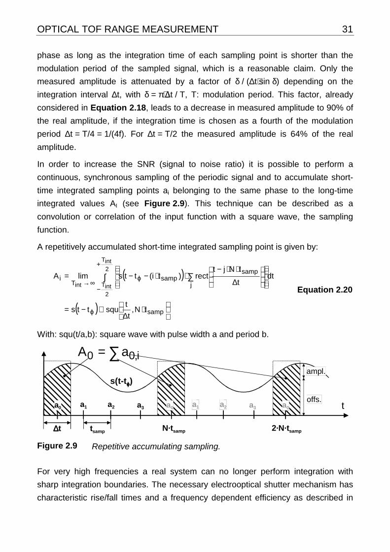
OPTICAL TOF RANGE MEASUREMENT 31 phase as long as the integration time of each sampling point is shorter than the
modulation period of the sampled signal, which is a reasonable claim. Only the
measured amplitude is attenuated by a factor of δ / (∆t⋅sin δ) depending on the
integration interval ∆t, with δ = π⋅∆t / T, T: modulation period. This factor, already
considered in Equation 2.18, leads to a decrease in measured amplitude to 90% of
the real amplitude, if the integration time is chosen as a fourth of the modulation
period ∆t = T/4 = 1/(4f). For ∆t = T/2 the measured amplitude is 64% of the real
amplitude.
In order to increase the SNR (signal to noise ratio) it is possible to perform a
continuous, synchronous sampling of the periodic signal and to accumulate short-
time integrated sampling points ai belonging to the same phase to the long-time
integrated values AI (see Figure 2.9). This technique can be described as a
convolution or correlation of the input function with a square wave, the sampling
function.
A repetitively accumulated short-time integrated sampling point is given by:
( )
( ) tN,t
tsqutts
dtt
tNjtrect)ti(ttslimA
samp
j
sampsamp
Ti
2intT
2intTint
⋅
∆⊗−=
∆
⋅⋅−⋅⋅−−=
ϕ
+
−
ϕ∞→
∫ ∑ Equation 2.20
With: squ(t/a,b): square wave with pulse width a and period b.
t
s(t-tϕϕϕϕ)
∆∆∆∆t tsamp N·tsamp 2·N·tsamp
a2 a3a1a0
∑= i,00 aA
a2 a3a1a0 a0
ampl.
offs.
Figure 2.9 Repetitive accumulating sampling.
For very high frequencies a real system can no longer perform integration with
sharp integration boundaries. The necessary electrooptical shutter mechanism has
characteristic rise/fall times and a frequency dependent efficiency as described in
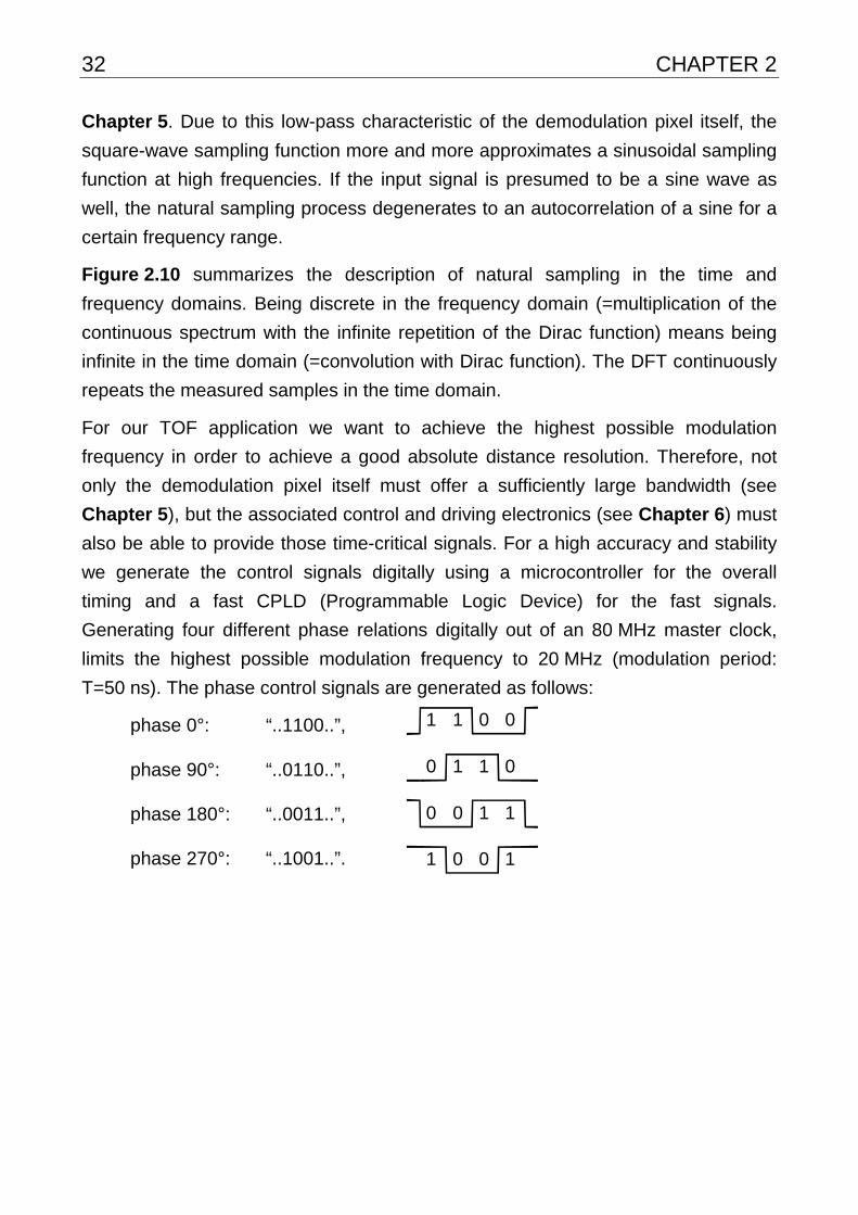
32 CHAPTER 2 Chapter 5. Due to this low-pass characteristic of the demodulation pixel itself, the
square-wave sampling function more and more approximates a sinusoidal sampling
function at high frequencies. If the input signal is presumed to be a sine wave as
well, the natural sampling process degenerates to an autocorrelation of a sine for a
certain frequency range.
Figure 2.10 summarizes the description of natural sampling in the time and
frequency domains. Being discrete in the frequency domain (=multiplication of the
continuous spectrum with the infinite repetition of the Dirac function) means being
infinite in the time domain (=convolution with Dirac function). The DFT continuously
repeats the measured samples in the time domain.
For our TOF application we want to achieve the highest possible modulation
frequency in order to achieve a good absolute distance resolution. Therefore, not
only the demodulation pixel itself must offer a sufficiently large bandwidth (see
Chapter 5), but the associated control and driving electronics (see Chapter 6) must
also be able to provide those time-critical signals. For a high accuracy and stability
we generate the control signals digitally using a microcontroller for the overall
timing and a fast CPLD (Programmable Logic Device) for the fast signals.
Generating four different phase relations digitally out of an 80 MHz master clock,
limits the highest possible modulation frequency to 20 MHz (modulation period:
T=50 ns). The phase control signals are generated as follows:
phase 0°: “..1100..”,
phase 90°: “..0110..”,
phase 180°: “..0011..”,
phase 270°: “..1001..”.
1 1
1 1
1 1
11
0
0 0
00
00
0
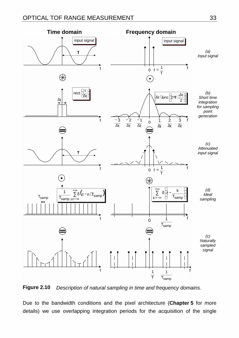
OPTICAL TOF RANGE MEASUREMENT 33
Time domain Frequency domain
∆t
t rect
t
t∆
t
( )∑∞+
−∞=⋅−δ
nsamp
sampTnt
T
1
f
t
1∆ t
2∆ t
3∆t
2∆−
t
1∆−
t
3∆−
0
∆⋅π⋅∆
2
tf2sinct
f
sampT
10
∑∞+
−∞=
−δ
k sampT
kf
t
T
input signal
fT
1f =0
input signal
t
T
fT
1f =0
sampT
t f
T
1
sampT
1
(a) Input signal
(b) Short time integration
for sampling point
generation
(c) Attenuated input signal
(d) Ideal
sampling
(c) Naturally sampled
signal
Figure 2.10 Description of natural sampling in time and frequency domains.
Due to the bandwidth conditions and the pixel architecture (Chapter 5 for more
details) we use overlapping integration periods for the acquisition of the single
34 CHAPTER 2 sampling points, i.e. the short time integration time is chosen to be half the
modulation period, ∆t=T/2=25 ns for 20 MHz modulation frequency. This is
possible, since the sampling points are acquired serially rather than in parallel.
Although the amplitude decreases to sinc(0.5π)=64% this operation mode results in
the best overall performance, since it offers the most efficient use of the available
optical power and additionally for shorter integration intervals a higher system
bandwidth would be required.
Spectral selectivity characteristic: influence of finite observation window
To describe the situation completely we have to consider the fact that the
observation window is finite. The size of the observation window is of essential
importance for the spectral selectivity characteristic of the measurement. Assuming
that other (asynchronously) modulated signals also reach the detector, it is obvious
that, for a relatively short integration time, superimposed frequency components
located near to the signal frequency will disturb the measurement. (In this context
we mean the overall integration time, not the short-time integration to acquire the
sampling points). This is a problem as long as the integration time is on the order of
the period of the beat frequency generated by the superposition of both received
signals. We will call these signals measurement signal and spurious signal from
now on, and for simplification we assume the same amplitude for both.
Again, as for the short-time integration of sampling point acquisition, the integration
or observation within a finite observation window (multiplication with a rect(t/Tw) in
the time domain) leads to a convolution with a sinc-function in the frequency
domain. The longer the overall integration time, the smaller is the width of the sinc
function. Thus the spectral selectivity between measurement and spurious signal
improves. These contents are illustrated in Figure 2.11.
OPTICAL TOF RANGE MEASUREMENT 35
t
WT
WT
trect
f
⋅⋅π
2
Tf2sinc W
t
t
measurement signal
spurious signal
resulting input signal
1f
2ft
f1f0
input signal
2f
f
spurious signalf
measurement signal
2f
1f
WT
1
t
WT
f1f0 2f
f∆
f
1f
0 2f
signal distortionby spurious signal
⋅∆⋅π
2
Tf2sinc W
Figure 2.11 Spectral selectivity of digital lock-in.
We only have to consider the superimposed signal power of the spurious signal’s
sinc-spectrum into the spectrum of the measurement signal at its center frequency.
This is because the DFT detection is only sensitive to discrete frequencies, as
36 CHAPTER 2 mentioned before. The demodulation result for the measurement signal is then
falsified due to frequency dispersion by:
⋅∆⋅π
2
Tf2sinc w Equation 2.21
With TW=observation window/ integration time and ∆f=difference frequency of
measurement and spurious signal.
If we postulate a signal suppression of better than 40 dB (factor 100) for
neighboring frequencies, we need to choose integration times as listed below:
f1 f2 ∆f TW
20 MHz 21.0000 MHz 1 MHz 100 µsec
20 MHz 20.1000 MHz 100 kHz 1 msec
20 MHz 20.0100 MHz 10 kHz 10 msec
20 MHz 20.0010 MHz 1 kHz 100 msec
20 MHz 20.0001 MHz 100 Hz 1 sec
These considerations are of special importance if two or more TOF cameras
observe the same area so that their radiation fields are superimposed. If for any
reason these modulation signals can’t be separated by using light of different
wavelengths, one might want to separate the signals by using slightly different
modulation frequencies. In that case the observation window defines the spectral
selectivity concerning modulation frequency. Note that the above estimation
presumes equal amplitudes of spurious signal and measurement signal.
2.2.2 Aliasing
Obviously the shape of the modulation signal has an influence on the measurement
result. As already mentioned, we only use four sampling points to sample the offset
containing signal. Therefore, Shannon’s law is only obeyed for a pure sinusoidal
wave. If we consider using a square-wave modulated signal (infinite spectrum),
taking only four sampling points will lead to aliasing effects. In most of the literature
aliasing is only treated together with the amplitude spectrum. We, however, are
especially interested in the influence of aliasing on the phase spectrum. For that
purpose we first take a simple signal consisting of a cosine wave and one harmonic
frequency of the same amplitude and triple frequency. This is to simplify the spectra
OPTICAL TOF RANGE MEASUREMENT 37 and algorithms in order to understand clearly and easily what happens to the phase
spectrum. In a next step we will transfer these results to a square wave. And lastly
we will simulate aliasing effects on several other waveforms, presuming DFT
detection with four sampling points.
An important boundary condition is the chosen integration interval for the sampling
point acquisition. As already discussed this is chosen to be half the modulation
period ∆t=T/2 in the following calculations. From Figure 2.8 we can conclude that,
for ∆t=T/2, all even harmonics of the basic frequency, namely 2f, 4f, 6f, … will be
suppressed and do not contribute to the demodulation result. This is because these
harmonics are eliminated by a zero crossing of the sinc-function. This simple
example shows the importance of the choice of ∆t for aliasing effects.
Aliasing phase error for 3f-harmonic using 4-tap DFT-detection.
In order to simplify explanations we use the expression “tap” for “sampling point”
from now on. We consider the input signal s(t) having a harmonic of triple base
frequency and amplitude “1”.
( ) ( )0000 3t3costcos)t(s ϕ−ω+ϕ−ω= Equation 2.22
The phase delay ϕ0 is caused by the distance dependent time delay in our TOF
application. This time delay causes a phase delay of 3ϕ0 in the 3f-harmonic
component.
Transformed into the Fourier domain we obtain the spectrum S(f):
( ) ( )( ) ( ) 00
00
3j0
3j0
j0
j0
e3e3
ee 2
1)f(S
ϕϕ−
ϕϕ−
⋅ω+ωδ+⋅ω−ωδ+
⋅ω+ωδ+⋅ω−ωδ=
Equation 2.23
Now we consider the integration of the taps, i.e. convolution of s(t) with rect(t/∆t)
and multiplication of S(f) with sinc(2π⋅f⋅∆t/2)=sinc(π⋅f⋅T/2) resulting in:
( ) ( )( )( ) ( )( )
3
a
3
2b and
2a with
e3e3b
eea 2
1)f(S
00
00
3j0
3j0
j0
j0int
−=π
−=π
=
⋅ω+ωδ+⋅ω−ωδ⋅+
⋅ω+ωδ+⋅ω−ωδ⋅=
ϕϕ−
ϕϕ−
Equation 2.24
The coefficients a and b are obtained by evaluation of sinc(π⋅f⋅T/2) at f=1/T and
f=3/T, respectively. By substituting b with a and considering -1 = ejπ = e-jπ we only
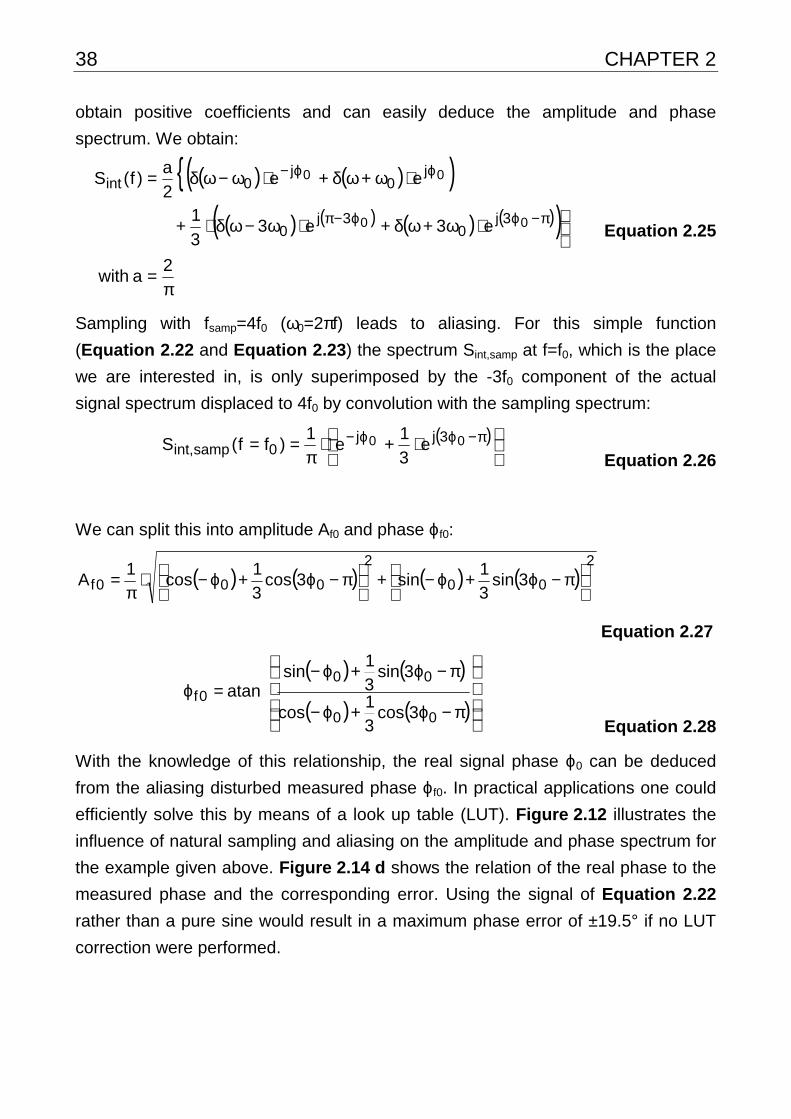
38 CHAPTER 2 obtain positive coefficients and can easily deduce the amplitude and phase
spectrum. We obtain:
( ) ( )( )( ) ( ) ( ) ( )( )
2
a with
e3e33
1
ee 2
a)f(S
00
00
3j0
3j0
j0
j0int
π=
⋅ω+ωδ+⋅ω−ωδ⋅+
⋅ω+ωδ+⋅ω−ωδ=
π−ϕϕ−π
ϕϕ−
Equation 2.25
Sampling with fsamp=4f0 (ω0=2πf) leads to aliasing. For this simple function
(Equation 2.22 and Equation 2.23) the spectrum Sint,samp at f=f0, which is the place
we are interested in, is only superimposed by the -3f0 component of the actual
signal spectrum displaced to 4f0 by convolution with the sampling spectrum:
( )
⋅+⋅
π== π−ϕϕ− 00 3jj
0sampint, e3
1e
1)ff(S
Equation 2.26
We can split this into amplitude Af0 and phase ϕf0:
( ) ( ) ( ) ( )2
00
2
000f 3sin3
1sin3cos
3
1cos
1A
π−ϕ+ϕ−+
π−ϕ+ϕ−⋅
π=
Equation 2.27
( ) ( )
( ) ( )
π−ϕ+ϕ−
π−ϕ+ϕ−=ϕ
00
000f
3cos3
1cos
3sin3
1sin
atan
Equation 2.28
With the knowledge of this relationship, the real signal phase ϕ0 can be deduced
from the aliasing disturbed measured phase ϕf0. In practical applications one could
efficiently solve this by means of a look up table (LUT). Figure 2.12 illustrates the
influence of natural sampling and aliasing on the amplitude and phase spectrum for
the example given above. Figure 2.14 d shows the relation of the real phase to the
measured phase and the corresponding error. Using the signal of Equation 2.22
rather than a pure sine would result in a maximum phase error of ±19.5° if no LUT
correction were performed.
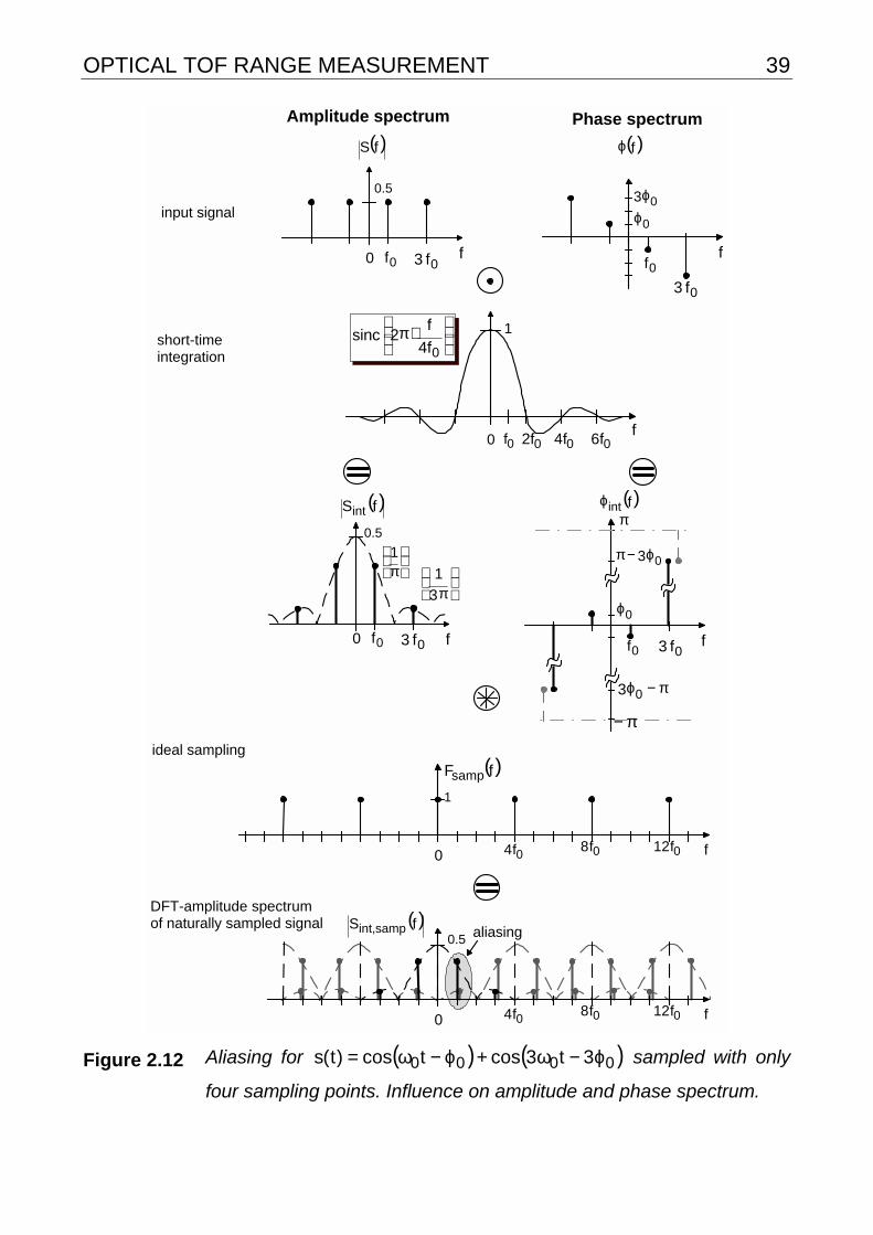
OPTICAL TOF RANGE MEASUREMENT 39
input signal
0
1
( )fFsamp
0f4 0f8 0f12 f
f0f
0f3
( )fϕ
0ϕ03ϕ
short-timeintegration
f
⋅π
0f4
f2sinc
0f 0f2 0f4 0f60
1
f0f 0f3
0ϕ
π
03ϕ−π
π−ϕ03
π−
( )fintϕ
ideal sampling
f0f0 0f3
( )fSint
0.5
π1
π3
1
0
0.5
0f4 0f8 0f12 f
aliasing( )fS sampint,
f0f0 0f3
( )fS
0.5
DFT-amplitude spectrum of naturally sampled signal
Amplitude spectrum Phase spectrum
Figure 2.12 Aliasing for ( ) ( )0000 3t3costcos)t(s ϕ−ω+ϕ−ω= sampled with only
four sampling points. Influence on amplitude and phase spectrum.
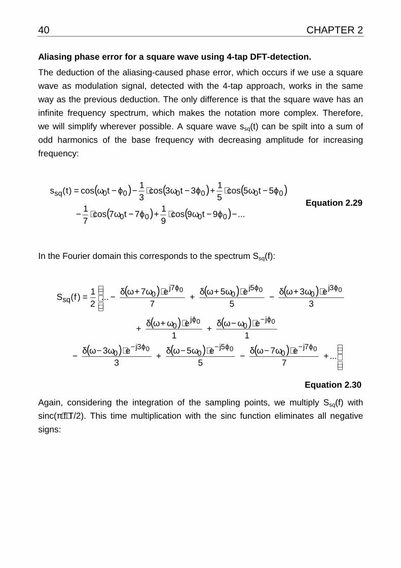
40 CHAPTER 2 Aliasing phase error for a square wave using 4-tap DFT-detection.
The deduction of the aliasing-caused phase error, which occurs if we use a square
wave as modulation signal, detected with the 4-tap approach, works in the same
way as the previous deduction. The only difference is that the square wave has an
infinite frequency spectrum, which makes the notation more complex. Therefore,
we will simplify wherever possible. A square wave ssq(t) can be spilt into a sum of
odd harmonics of the base frequency with decreasing amplitude for increasing
frequency:
( ) ( ) ( )
( ) ( ) ...9t9cos9
17t7cos
7
1
5t5cos5
13t3cos
3
1tcos)t(s
0000
000000sq
−ϕ−ω⋅+ϕ−ω⋅−
ϕ−ω⋅+ϕ−ω⋅−ϕ−ω= Equation 2.29
In the Fourier domain this corresponds to the spectrum Ssq(f):
( ) ( ) ( )
( ) ( )
( ) ( ) ( )
+⋅ω−ωδ−⋅ω−ωδ+⋅ω−ωδ−
⋅ω−ωδ+⋅ω+ωδ+
⋅ω+ωδ−⋅ω+ωδ+⋅ω+ωδ−=
ϕ−ϕ−ϕ−
ϕ−ϕ
ϕϕϕ
... 7
e7
5
e5
3
e3
1
e
1
e
3
e3
5
e5
7
e7 ...
2
1)f(S
000
00
000
7j0
5j0
3j0
j0
j0
3j0
5j0
7j0
sq
Equation 2.30
Again, considering the integration of the sampling points, we multiply Ssq(f) with
sinc(π⋅f⋅T/2). This time multiplication with the sinc function eliminates all negative
signs:

OPTICAL TOF RANGE MEASUREMENT 41
( ) ( ) ( )
( ) ( )
( ) ( ) ( )
+π⋅
⋅ω−ωδ+π⋅
⋅ω−ωδ+π⋅
⋅ω−ωδ+
π⋅
⋅ω−ωδ+π⋅
⋅ω+ωδ+
π⋅
⋅ω+ωδ+π⋅
⋅ω+ωδ+π⋅
⋅ω+ωδ+=
ϕ−ϕ−ϕ−
ϕ−ϕ
ϕϕϕ
...
2
77
e7
2
55
e5
2
33
e3
21
e
21
e
2
33
e3
2
55
e5
2
77
e7 ...
2
1)f(S
000
00
000
7j0
5j0
3j0
j0
j0
3j0
5j0
7j0
int,sq
Equation 2.31
Now we sample with fsamp=4f0 (ω0=2πf) and observe aliasing, as in the previously examined case. The spectrum at f=f0 ( )0sampint,,sq ffS = , looks like this:
++++
+
+++π
==
ϕ−ϕ−ϕ−ϕ−
ϕϕϕ
... 169
e
81
e
25
e
1
e
9
e
49
e
121
e ...
1)ff(S
0000
000
13j9j5jj
3j7j11j
0sampint,,sq
Equation 2.32
We can split this into amplitude Asq,f0 and phase ϕsq,f0:
( ) ( ) ( )
( ) ( ) ( ) 2000
2000
0f,sq
...25
5sin
1
sin
9
3sin...
...25
5cos
1
cos
9
3cos...
1
A
+ϕ−+ϕ−+ϕ++
+ϕ−+ϕ−+ϕ+
⋅π
=
Equation 2.33
( ) ( ) ( )
( ) ( ) ( ) ...
25
5cos
1
cos
9
3cos...
...25
5sin
1
sin
9
3sin...
atan000
000
0f,sq
+ϕ−+ϕ−+ϕ+
+ϕ−+ϕ−+ϕ+=ϕ
Equation 2.34
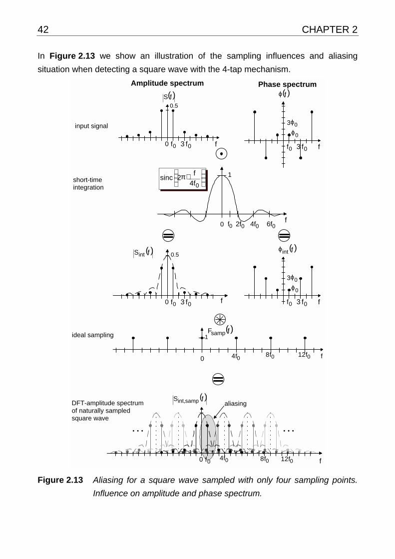
42 CHAPTER 2 In Figure 2.13 we show an illustration of the sampling influences and aliasing
situation when detecting a square wave with the 4-tap mechanism.
input signal
0
1( )fFsamp
0f4 0f8 0f12 f
( )fϕ
0ϕ03ϕ
f0f 0f3
short-timeintegration
f
⋅π
0f4
f2sinc
0f 0f2 0f4 0f60
1
ideal sampling
( )fSint
f0f0 0f3
0.5
DFT-amplitude spectrum of naturally sampled square wave
Amplitude spectrum Phase spectrum
f0f0 0f3
( )fS0.5
( )fintϕ
0ϕ03ϕ
f0f 0f3
f0f0
( )fS sampint,
0f4
aliasing
0f8 0f12
Figure 2.13 Aliasing for a square wave sampled with only four sampling points.
Influence on amplitude and phase spectrum.
OPTICAL TOF RANGE MEASUREMENT 43 From Equation 2.34 we can deduce that there is a predictable connection between
the measured phase and the real phase. (See also Figure 2.14 k.)
Aliasing phase error for different input signals using 4-tap DFT-detection.
In addition to these analytical considerations, it is helpful to use numerical
simulation in order to obtain the relation between measured and real phase for
periodic input signals differing from the pure sinusoidal wave. We have performed
those simulations for the input signals discussed above and also for several other
input signals. The results are shown in Figure 2.14, which shows the input signal,
the measured and real phase as well as the predictable phase error. Figure 2.14
(a), (c), (e) and (g) show that, for ∆t=T/2, even harmonics do not cause any phase
error (see above). Figure 2.14 (i), (j) and (l) confirm that the short-time integration
∆t plays an important role.
The following table lists the harmonics and their coefficients used for the simulation.
It also summarizes the resulting maximum phase error if no LUT correction is
performed.
Modulation signal even harmonics odd harmonics Error in degrees
cos - - 0 cos2 - - 0 cos(x) + cos(2x) 2 - 0 cos(x) + cos(4x) 4 - 0 cos(x) + cos(6x) 6 - 0 cos(x) + cos(3x) - 3 ± 19.5 cos(x) + cos(5x) - 5 ± 11.5 cos(x) + cos(7x) - 7 ± 8.2
cos(x) + cos(3x), ∆t=T/3 - 3 ± 0.3
cos(x) + cos(5x), ∆t=T/5 - 5 0
square wave - 1/3⋅3, 1/5⋅5, 1/7*7, … ± 4.2
square wave, ∆t=T/3 - 1/3⋅3, 1/5⋅5, 1/7⋅7, … ± 3.4 triangle - 1/9⋅3, 1/25⋅5, 1/49⋅7, 1/81⋅9, … ± 2.6 ramp 1/2⋅2, 1/4⋅4, 1/6⋅6, … 1/3⋅3, 1/5⋅5, 1/7⋅7, … ± 4.2 square wave with linear falling edge
combinations of above ± 5.4
square wave with exponential falling edge
combinations of above ± 3.5
44 CHAPTER 2
0 100 200 300 400 500 600 700 800 900 10000
0.5
1
MODULATION SIGNAL
0 50 100 150 200 250 300 3500
200
400
CORRECT PHASE AND CALCULATED PHASE
0 50 100 150 200 250 300 350-1
0
1
ERROR = ± 0
cos
(a), (b)
0 100 200 300 400 500 600 700 800 900 10000
0.5
1
MODULATION SIGNAL
0 50 100 150 200 250 300 3500
200
400
CORRECT PHASE AND CALCULATED PHASE
0 50 100 150 200 250 300 350-1
0
1
ERROR = ± 0
cos2
0 100 200 300 400 500 600 700 800 900 1000-0.5
0
0.5
1
MODULATION SIGNAL
0 50 100 150 200 250 300 3500
200
400
CORRECT PHASE AND CALCULATED PHASE
0 50 100 150 200 250 300 350-1
0
1
ERROR = ± 0
cos(x) + cos(2x)
(c), (d)
0 100 200 300 400 500 600 700 800 900 1000
0
0.5
1
MODULATION SIGNAL
0 50 100 150 200 250 300 3500
200
400
CORRECT PHASE AND CALCULATED PHASE
0 50 100 150 200 250 300 350
-10
0
10
ERROR = ± 19.46
cos(x) + cos(3x)
0 100 200 300 400 500 600 700 800 900 1000
0
0.5
1
MODULATION SIGNAL
0 50 100 150 200 250 300 3500
200
400
CORRECT PHASE AND CALCULATED PHASE
0 50 100 150 200 250 300 350-1
0
1
ERROR = ± 0
cos(x) + cos(4x)
(e), (f)
0 100 200 300 400 500 600 700 800 900 1000
0
0.5
1
MODULATION SIGNAL
0 50 100 150 200 250 300 3500
200
400
CORRECT PHASE AND CALCULATED PHASE
0 50 100 150 200 250 300 350
-10
0
10
ERROR = ± 11.53
cos(x) + cos(5x)
0 100 200 300 400 500 600 700 800 900 1000
0
0.5
1
MODULATION SIGNAL
0 50 100 150 200 250 300 3500
200
400
CORRECT PHASE AND CALCULATED PHASE
0 50 100 150 200 250 300 350-1
0
1
ERROR = ± 0
cos(x) + cos(6x)
(g), (h)
0 100 200 300 400 500 600 700 800 900 1000
0
0.5
1
MODULATION SIGNAL
0 50 100 150 200 250 300 3500
200
400
CORRECT PHASE AND CALCULATED PHASE
0 50 100 150 200 250 300 350
-5
0
5
ERROR = ± 8.21
cos(x) + cos(7x)
Figure 2.14 (a-h) Influence of modulation signal on phase accuracy I.
OPTICAL TOF RANGE MEASUREMENT 45
0 100 200 300 400 500 600 700 800 900 1000
0
0.5
1
MODULATION SIGNAL
0 50 100 150 200 250 300 3500
200
400
CORRECT PHASE AND CALCULATED PHASE
0 50 100 150 200 250 300 350-1
0
1
ERROR = ± 0.28
cos(x) + cos(3x), ∆t=T/3
(i), (j)
0 100 200 300 400 500 600 700 800 900 1000
0
0.5
1
MODULATION SIGNAL
0 50 100 150 200 250 300 3500
200
400
CORRECT PHASE AND CALCULATED PHASE
0 50 100 150 200 250 300 350-1
0
1
ERROR = ± 0
cos(x) + cos(5x), ∆t=T/5
0 100 200 300 400 500 600 700 800 900 1000
0
0.5
1
MODULATION SIGNAL
0 50 100 150 200 250 300 3500
200
400
CORRECT PHASE AND CALCULATED PHASE
0 50 100 150 200 250 300 350-4
-2
0
2
4
ERROR = ± 4.19
square wave
(k), (l)
0 100 200 300 400 500 600 700 800 900 1000
0
0.5
1
MODULATION SIGNAL
0 50 100 150 200 250 300 3500
200
400
CORRECT PHASE AND CALCULATED PHASE
0 50 100 150 200 250 300 350
-2
0
2
ERROR = ± 3.43
square wave, ∆t=T/3
0 100 200 300 400 500 600 700 800 900 1000
0
0.5
1
MODULATION SIGNAL
0 50 100 150 200 250 300 3500
200
400
CORRECT PHASE AND CALCULATED PHASE
0 50 100 150 200 250 300 350-5
0
5
ERROR = ± 5.4
square wave with linear falling edge
(m), (n)
0 100 200 300 400 500 600 700 800 900 1000
0
0.5
1
MODULATION SIGNAL
0 50 100 150 200 250 300 3500
200
400
CORRECT PHASE AND CALCULATED PHASE
0 50 100 150 200 250 300 350
-2
0
2
4
ERROR = ± 3.525
square wave with exponentially
falling edge
0 100 200 300 400 500 600 700 800 900 10000
0.5
1
MODULATION SIGNAL
0 50 100 150 200 250 300 3500
200
400
CORRECT PHASE AND CALCULATED PHASE
0 50 100 150 200 250 300 350-4
-2
0
2
4
ERROR = ± 4.19
ramp
(o), (p)
0 100 200 300 400 500 600 700 800 900 10000
0.5
1
MODULATION SIGNAL
0 50 100 150 200 250 300 3500
200
400
CORRECT PHASE AND CALCULATED PHASE
0 50 100 150 200 250 300 350
-2
0
2
ERROR = ± 2.57
triangle
Figure 2.14 (i-p) Influence of modulation signal on phase accuracy II.

46 CHAPTER 2 2.2.3 Influence of system non-linearities
Generally, the transfer characteristic of all components involved in the analogous
output, ranging from the on chip output amplifier to the digitization, is not exactly
linear. In this section we describe the influence of quadratic non-linearities on the
measured phase using the 4-tap algorithm.
From the four acquired sampling points A0..A3 the phase ϕ is calculated using the
following equation:
−−
=ϕ31
20
AA
AAarctan Equation 2.35
Considering linear and quadratic distortions in the transfer function leads to the
measurement of a⋅Ai + b⋅Ai2 rather than Ai. For the measured phase ϕmeas this
means:
( ) ( )( ) ( )
−⋅+−⋅
−⋅+−⋅=ϕ
23
2131
22
2020
measAAbAAa
AAbAAaarctan Equation 2.36
This can be rewritten as:
( ) ( ) ( )
( ) ( ) ( )
+⋅−⋅+−
+⋅−⋅+−=ϕ
313131
202020
measAAAA
a
bAA
AAAAa
bAA
arctan Equation 2.37
As can be seen from Figure 2.7, the sum “A0+A2” and “A1+A3” equal two times the
offset B. This is because cos(x) = -cos(x+180°). So we obtain:
( ) ( )
( ) ( )
( )
( )
ϕ=
−−
=
−⋅
⋅⋅+
−⋅
⋅⋅+
=
−⋅⋅⋅+−
−⋅⋅⋅+−=ϕ
31
20
31
20
3131
2020
meas
AA
AAarctan
AAa
bB21
AAa
bB21
arctanAA
a
bB2AA
AAa
bB2AA
arctan
Equation 2.38
This means that the 4-tap algorithm is not sensitive to linear or quadratic distortions
in the analogous transfer characteristic.
OPTICAL TOF RANGE MEASUREMENT 47 2.2.4 Summary
To summarize, demodulation pixels can be realized by giving them the ability to
sample the incoming light in the time domain synchronously with its modulation
frequency. With the DFT it is only possible to measure discrete frequencies. In
order to enlarge the SNR, the sampling process must be repeated a large number
of times, integrating the small signal amounts of each sampling point to a larger
signal value. This successive integration of the sampling points (1) sharpens the
system’s sensitivity to discrete frequencies only: spectral selectivity, (2) lowers the
(unwanted) sensitivity to neighboring frequency components and (3) improves the
SNR by increasing the signal strength. Due to this frequency selective integrating
nature we also call our pixels “lock-in pixels”. Like a lock-in amplifier, they are only
sensitive to the modulation frequency itself.
With analytical calculations as well as some numerical simulations we have shown
that the 4-tap algorithm is not sensitive to quadratic system non-linearties and is
also insensitive to even harmonics of the modulation signal. Odd harmonics, as
present in a square wave for example disturb the measured phase. This is caused
by aliasing. In practice this is not a serious problem, since there is (usually) an
unambiguous relationship between the real phase and the measured phase, so that
the error can be corrected using a look up table (LUT). In the TOF application such
a LUT correction was not necessary due to the low pass characteristics of both the
demodulation pixels and the LED illumination. Although the LEDs are controlled by
a digital signal (ideally a square wave), their output at 20 MHz is more sinusoidal
(c.f. Chapter 5).

SOLID-STATE IMAGE SENSING 49
3. Solid-state image sensing
Solid-state imaging has experienced a rapid growth, especially in the last ten years.
This development has benefited from the steady improvements and miniaturization
in the semiconductor industry and is also part of today’s multimedia revolution. The
first semiconductor solid-state imagers were photodiode arrays, where each diode
was directly connected to the output by a metal wire. The large capacitance of
these metal wires, resulting in a relatively slow signal readout speed and poor noise
performance was, however, the killing factor that prevented a wide propagation of
photodiode arrays, at least at that time.
In 1970 Boyle introduced a new, amazingly simple device for semiconductor image
sensing [BOY, AME], the so-called charge coupled device: CCD. These elements
collect optically generated charge carriers under locally separated photogates.
Bundled to charge packets in the single pixels, the optically generated charge
carriers can then, after a certain integration time, be moved through the
semiconductor into certain storage areas by making use of the charge-coupling
principle. This method is explained in more detail below. From these storage areas
they are then sequentially shifted to one output stage, where the charge is
converted into a voltage (Figure 3.1 c.) The use of only one low-capacitance output
stage is still one of the essential advantages of CCDs since it means both low noise
and very high homogeneity between the single pixels. Additionally, with the charge-
coupling principle, it is possible to perform certain sorts of signal processing [SP4].
The essentially noise-free charge addition of single charge carriers is only one
example of CCD’s amazing charge domain signal processing capabilities. However,
to operate CCDs, voltages between 10 and 20V are necessary, very often requiring
large currents of up to some amperes, since capacitances of some nanofarads
have to be charged and discharged within nanoseconds. This results in relatively
large power dissipation, a major drawback of CCDs compared to some of today’s
CMOS APS sensors. Other weak points of CCDs are the facts that (1) the complete
sensor always has to be read out in order to reset the pixel values and to start a
new image acquisition and (2) the image is after-exposed during readout, known as

50 CHAPTER 3
the smearing effect, resulting in lines in the image having an origin in very bright
points [TEU].
(a)
(c)
DestinationStart
CCD
Destination
CMOS-APS
optical generationof signal charge
chargetransport
charge to voltageconversion
Column select
Row
sele
ct
OutputOutput
Start
charge to voltageconversion in the
output stage
charge to voltageconversion in the pixel
(b)
(d)
Figure 3.1 CCD and CMOS-APS principle: Hydrostatic equivalent and principle
architecture.
Due to the steady miniaturization in microelectronics, photodiode arrays, in the form
of CMOS APS sensors (Active Pixel Sensor), have experienced a sort of
renaissance in recent years. They are gradually beginning to replace CCDs in
certain market areas, such as low-cost applications or applications where certain
features/functionality are required (high speed, low power, logarithmic response, no
blooming or smearing, temporal convolution, …). CMOS APS sensors, in contrast
to the classical photodiode arrays, give each pixel its own buffer amplifier, which
converts the charge signal into a voltage (or current) within the pixel. With this
principle it is avoided that the small photocurrent of each pixel has to drive the
relatively large capacity of metal wires. The optical signal information is then read
SOLID-STATE IMAGE SENSING 51
out by sequentially connecting the low impedance pixel-amplifier to the output,
rather than the high-impedance nodes of the photodiodes. The APS principle,
sketched in Figure 3.1 d, offers low conversion capacitance and hence good
sensitivity and low noise performance, gradually approaching CCD performance.
Another advantage is the possibility to read out and reset single pixels by selecting
them with the proper address at the row- and column- address decoder. This
makes it possible to define so-called regions of interest (ROI) and to increase the
image frame rate locally. Also, in general each pixel can be operated with an
individual integration time. However, compared to CCDs, CMOS APS imagers often
have a poorer image quality. This is because they suffer from an effect known as
fixed pattern noise (FPN): due to variations in oxide thickness, size of gate area
and doping concentrations over the sensor, each pixel has a different offset (up to
some 10mV differences) and a slightly different gain, (which can usually be
neglected). Therefore, external FPN correction is required; an effort, which is not
necessary if using CCDs. FPN correction subtracts a locally stored dark image from
the actually acquired image, thus eliminating the fixed pattern noise. Recently,
approaches such as sensor-integrated correlated double sampling (CDS) or the
active column principle have been demonstrated, offering ways to overcome the
FPN problem [HOP, DEC, VOG].
The basic difference between CCD (charge domain signal processing) and CMOS
APS (in general voltage domain signal processing) is illustrated by the hydrostatic
equivalents in Figure 3.1 a+b. CCD imagers locally collect charge carriers to
transport them physically to the output stage, where they are converted into a
voltage. In contrast, CMOS APS sensors generate the signal voltage already in the
pixel. The information can then be directly connected to the output.
Both CCD and CMOS APS are realized in MOS-technologies (Metal Oxide
Semiconductor), mostly in silicon. The special processes, however, are optimized
towards different goals. So it is usually not possible to realize good CCDs with a
CMOS process or to realize efficient CMOS circuitry in a CCD technology. An
overview of the most important and relevant electrical and optical properties of
silicon for image sensing is given in Section 3.1. The following sections then focus
on specific principles and properties of CCD (Section 3.2) and CMOS APS sensors
(Section 3.3). More detailed information can be found in the references [TEU, BEY,
SEQ, SZ1, SZ2, PS1, PS2, FOS].
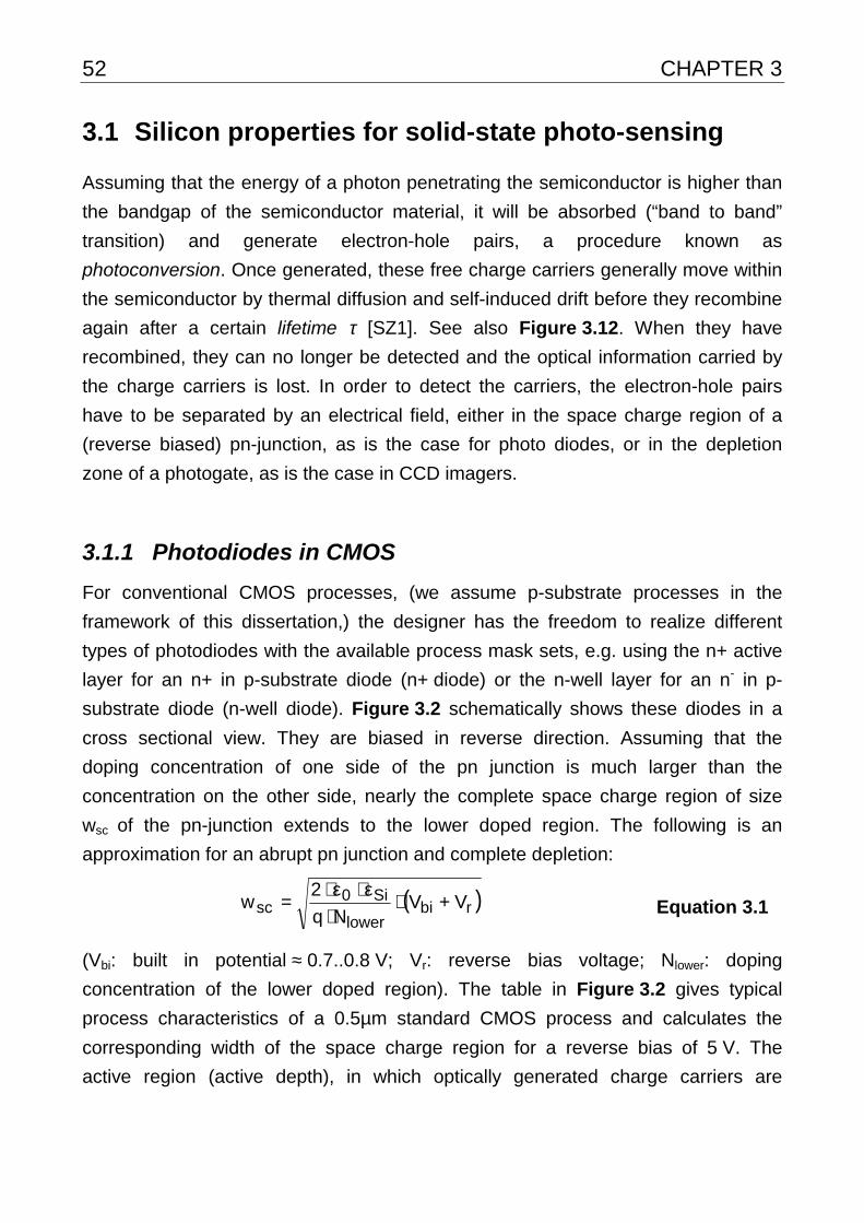
52 CHAPTER 3
3.1 Silicon properties for solid-state photo-sensing
Assuming that the energy of a photon penetrating the semiconductor is higher than
the bandgap of the semiconductor material, it will be absorbed (“band to band”
transition) and generate electron-hole pairs, a procedure known as
photoconversion. Once generated, these free charge carriers generally move within
the semiconductor by thermal diffusion and self-induced drift before they recombine
again after a certain lifetime τ [SZ1]. See also Figure 3.12. When they have
recombined, they can no longer be detected and the optical information carried by
the charge carriers is lost. In order to detect the carriers, the electron-hole pairs
have to be separated by an electrical field, either in the space charge region of a
(reverse biased) pn-junction, as is the case for photo diodes, or in the depletion
zone of a photogate, as is the case in CCD imagers.
3.1.1 Photodiodes in CMOS
For conventional CMOS processes, (we assume p-substrate processes in the
framework of this dissertation,) the designer has the freedom to realize different
types of photodiodes with the available process mask sets, e.g. using the n+ active
layer for an n+ in p-substrate diode (n+ diode) or the n-well layer for an n- in p-
substrate diode (n-well diode). Figure 3.2 schematically shows these diodes in a
cross sectional view. They are biased in reverse direction. Assuming that the
doping concentration of one side of the pn junction is much larger than the
concentration on the other side, nearly the complete space charge region of size
wsc of the pn-junction extends to the lower doped region. The following is an
approximation for an abrupt pn junction and complete depletion:
( )rbilower
Si0sc VV
Nq
2w +⋅
⋅ε⋅ε⋅
= Equation 3.1
(Vbi: built in potential ≈ 0.7..0.8 V; Vr: reverse bias voltage; Nlower: doping
concentration of the lower doped region). The table in Figure 3.2 gives typical
process characteristics of a 0.5µm standard CMOS process and calculates the
corresponding width of the space charge region for a reverse bias of 5 V. The
active region (active depth), in which optically generated charge carriers are

SOLID-STATE IMAGE SENSING 53
immediately separated and captured, extends up to d0 + wsc, where d0 is the
position of the pn-junction.
Diffusion Depth of
junction Doping concentration
n+ diffusion 200 nm 2⋅1020 cm-3
n-well 3700 nm 5⋅1016 cm-3
p-substrate 5⋅1015 cm-3
Photodiode wsc for Vr=5 V Active depth
(wsc + junct. depth)
n+ diode 1.2 µm 1.4 µm
n-well diode 1.2 µm 4.9 µm
VSSVDD VSSVDD
n+ diode
p- (substrate) n- (n-well) p+ n+
VSSVDD VSSVDD
n-well diode
Figure 3.2 Realizations of photodiodes in a CMOS process. The tables give
typical values of doping concentration and depth of the diffusion
regions for 0.5µm CMOS process. Also the width of the space
charge region is calculated.
Penetration depth of light
The absorption of photons entering the semiconductor material is a statistical
process. The sites of photon-absorption are statistically distributed with an
exponential dependence of distance from the semiconductor surface and
wavelength of the incoming light. The distance where an amount of %37e
1 = of the
total photon flux Φ(x) is already absorbed is called the penetration depth. That is
the inverse of the absorption constant α [Sze].
( )
−⋅α− ⋅Φ=⋅Φ=Φ depth npenetratio
x
ox
o e e)x( Equation 3.2
Figure 3.3 illustrates the exponential attenuation of the photon flux in silicon.
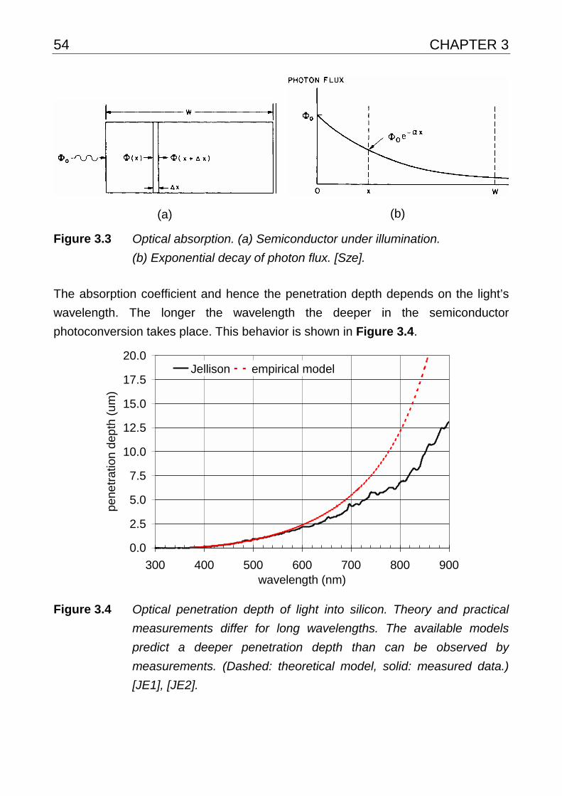
54 CHAPTER 3
(a)
(b)
Figure 3.3 Optical absorption. (a) Semiconductor under illumination.
(b) Exponential decay of photon flux. [Sze].
The absorption coefficient and hence the penetration depth depends on the light’s
wavelength. The longer the wavelength the deeper in the semiconductor
photoconversion takes place. This behavior is shown in Figure 3.4.
0.0
2.5
5.0
7.5
10.0
12.5
15.0
17.5
20.0
300 400 500 600 700 800 900wavelength (nm)
pene
tratio
n d
ep
th (
um
)
Jellison empirical model
Figure 3.4 Optical penetration depth of light into silicon. Theory and practical
measurements differ for long wavelengths. The available models
predict a deeper penetration depth than can be observed by
measurements. (Dashed: theoretical model, solid: measured data.)
[JE1], [JE2].
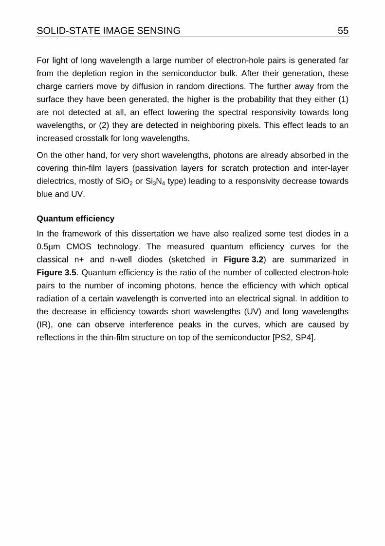
SOLID-STATE IMAGE SENSING 55
For light of long wavelength a large number of electron-hole pairs is generated far
from the depletion region in the semiconductor bulk. After their generation, these
charge carriers move by diffusion in random directions. The further away from the
surface they have been generated, the higher is the probability that they either (1)
are not detected at all, an effect lowering the spectral responsivity towards long
wavelengths, or (2) they are detected in neighboring pixels. This effect leads to an
increased crosstalk for long wavelengths.
On the other hand, for very short wavelengths, photons are already absorbed in the
covering thin-film layers (passivation layers for scratch protection and inter-layer
dielectrics, mostly of SiO2 or Si3N4 type) leading to a responsivity decrease towards
blue and UV.
Quantum efficiency
In the framework of this dissertation we have also realized some test diodes in a
0.5µm CMOS technology. The measured quantum efficiency curves for the
classical n+ and n-well diodes (sketched in Figure 3.2) are summarized in
Figure 3.5. Quantum efficiency is the ratio of the number of collected electron-hole
pairs to the number of incoming photons, hence the efficiency with which optical
radiation of a certain wavelength is converted into an electrical signal. In addition to
the decrease in efficiency towards short wavelengths (UV) and long wavelengths
(IR), one can observe interference peaks in the curves, which are caused by
reflections in the thin-film structure on top of the semiconductor [PS2, SP4].
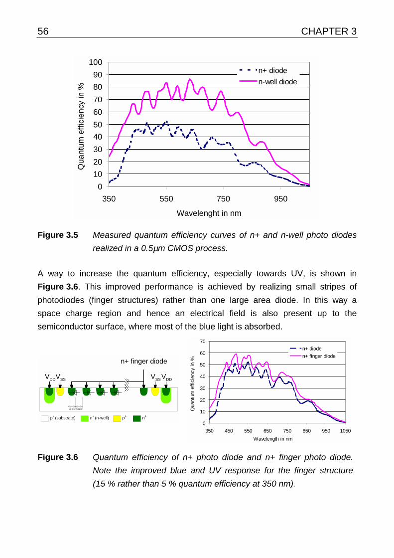
56 CHAPTER 3
0
10
20
30
40
50
60
70
80
90
100
350 550 750 950
Wavelenght in nm
Qua
ntum
eff
icie
ncy
in %
n+ diode
n-well diode
Figure 3.5 Measured quantum efficiency curves of n+ and n-well photo diodes
realized in a 0.5µm CMOS process.
A way to increase the quantum efficiency, especially towards UV, is shown in
Figure 3.6. This improved performance is achieved by realizing small stripes of
photodiodes (finger structures) rather than one large area diode. In this way a
space charge region and hence an electrical field is also present up to the
semiconductor surface, where most of the blue light is absorbed.
p- (substrate) n- (n-well) p+ n+
VSSVDD VSSVDD
n+ finger diode
1.2µm 0.8µm
0
10
20
30
40
50
60
70
350 450 550 650 750 850 950 1050
Wavelength in nm
Qua
ntum
eff
icie
ncy
in %
n+ diode
n+ finger diode
Figure 3.6 Quantum efficiency of n+ photo diode and n+ finger photo diode.
Note the improved blue and UV response for the finger structure
(15 % rather than 5 % quantum efficiency at 350 nm).
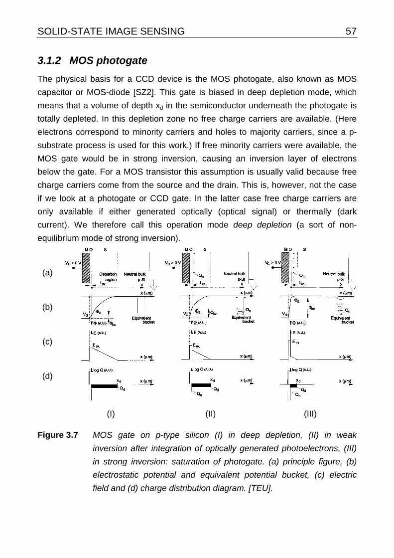
SOLID-STATE IMAGE SENSING 57
3.1.2 MOS photogate
The physical basis for a CCD device is the MOS photogate, also known as MOS
capacitor or MOS-diode [SZ2]. This gate is biased in deep depletion mode, which
means that a volume of depth xd in the semiconductor underneath the photogate is
totally depleted. In this depletion zone no free charge carriers are available. (Here
electrons correspond to minority carriers and holes to majority carriers, since a p-
substrate process is used for this work.) If free minority carriers were available, the
MOS gate would be in strong inversion, causing an inversion layer of electrons
below the gate. For a MOS transistor this assumption is usually valid because free
charge carriers come from the source and the drain. This is, however, not the case
if we look at a photogate or CCD gate. In the latter case free charge carriers are
only available if either generated optically (optical signal) or thermally (dark
current). We therefore call this operation mode deep depletion (a sort of non-
equilibrium mode of strong inversion).
(a)
(b)
(c)
(d)
(I) (II) (III)
Figure 3.7 MOS gate on p-type silicon (I) in deep depletion, (II) in weak
inversion after integration of optically generated photoelectrons, (III)
in strong inversion: saturation of photogate. (a) principle figure, (b)
electrostatic potential and equivalent potential bucket, (c) electric
field and (d) charge distribution diagram. [TEU].

58 CHAPTER 3
The different operation modes of the MOS gate are illustrated in Figure 3.7.
Figure 3.7 (I) shows the conditions when no free charge carriers are available. This
causes the depletion region to extend deep into the semiconductor resulting in a
deep space charge region (deep depletion). This mode can be interpreted as an
empty potential bucket, since it offers the capability to store electrons in the same
way that an empty water bucket offers the possibility to be filled with water.
With the (preferentially) optical generation of electron hole pairs free charge carriers
become available. The electron-hole pairs are separated in such a way that the
electrons (minority carriers) are collected at the semiconductor surface while the
holes (majority carriers) are rejected into the semiconductor bulk, where they
recombine after a certain lifetime. The electrons begin to form an inversion layer
and at the same time decrease the depth of the space charge region. This mode is
known as weak inversion. Continuing the comparison with the water bucket, this
integration process of optically generated electrons corresponds to filling the bucket
with water (Figure 3.7 (II)). We call the sum of integrated electrons, which are
acquired in the potential bucket, charge packets.
After a certain number of electrons are generated, the potential bucket will be filled
and no more free charge carriers can be held by the MOS diode (Figure 3.7 (III)).
This mode is known as strong inversion. It is the equilibrium condition of the MOS
diode for the gate voltage applied. It is also the mode a MOS transistor would be in
for the applied voltage, since, in contrast to the MOS capacitor the MOS transistor
offers the required number of free electrons directly from its source and drain. In the
CCD application strong inversion is the point which limits the charge handling
capability of the CCD gate. If more electrons were generated, they would move to a
neighboring pixel, a process called blooming.
Width of depletion region
The width of the depletion region xd, and thus the size of the “capture volume”, as a
function of the doping concentration NA (p-type substrate) and the gate voltage VG
is given by:
A
sSi0d Nq
2x
⋅Φ⋅ε⋅ε⋅= Equation 3.3
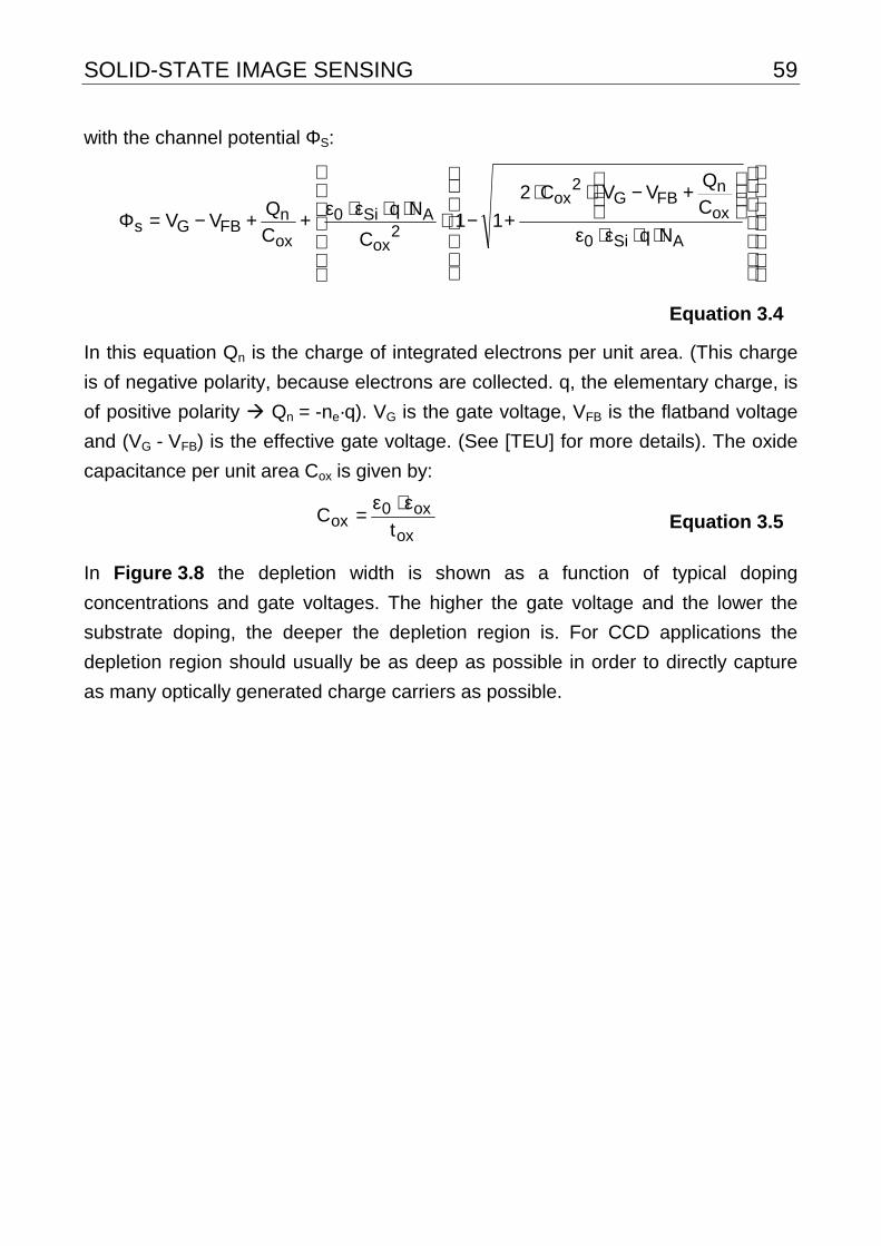
SOLID-STATE IMAGE SENSING 59
with the channel potential ΦS:
⋅⋅ε⋅ε
+−⋅⋅
+−⋅⋅⋅ε⋅ε++−=ΦASi0
ox
nFBG
2ox
2ox
ASi0
ox
nFBGs Nq
C
QVVC2
11C
Nq
C
QVV
Equation 3.4
In this equation Qn is the charge of integrated electrons per unit area. (This charge
is of negative polarity, because electrons are collected. q, the elementary charge, is
of positive polarity ! Qn = -ne·q). VG is the gate voltage, VFB is the flatband voltage
and (VG - VFB) is the effective gate voltage. (See [TEU] for more details). The oxide
capacitance per unit area Cox is given by:
ox
ox0ox t
Cε⋅ε= Equation 3.5
In Figure 3.8 the depletion width is shown as a function of typical doping
concentrations and gate voltages. The higher the gate voltage and the lower the
substrate doping, the deeper the depletion region is. For CCD applications the
depletion region should usually be as deep as possible in order to directly capture
as many optically generated charge carriers as possible.
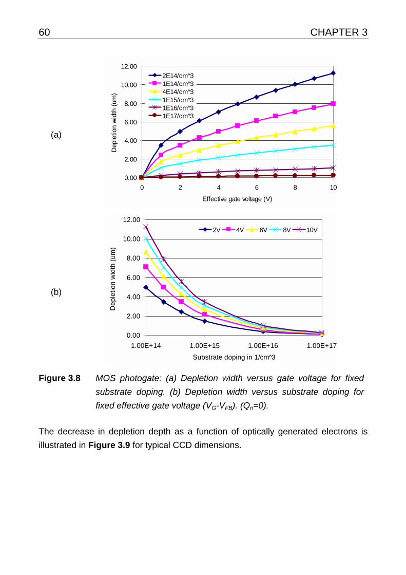
60 CHAPTER 3
(a)
0.00
2.00
4.00
6.00
8.00
10.00
12.00
0 2 4 6 8 10
Effective gate voltage (V)
Dep
letio
n w
idth
(um
)
2E14/cm^31E14/cm^34E14/cm^31E15/cm^31E16/cm^31E17/cm^3
(b)
0.00
2.00
4.00
6.00
8.00
10.00
12.00
1.00E+14 1.00E+15 1.00E+16 1.00E+17
Substrate doping in 1/cm^3
De
ple
tion
wid
th (
um
)
2V 4V 6V 8V 10V
Figure 3.8 MOS photogate: (a) Depletion width versus gate voltage for fixed
substrate doping. (b) Depletion width versus substrate doping for
fixed effective gate voltage (VG-VFB). (Qn=0).
The decrease in depletion depth as a function of optically generated electrons is
illustrated in Figure 3.9 for typical CCD dimensions.
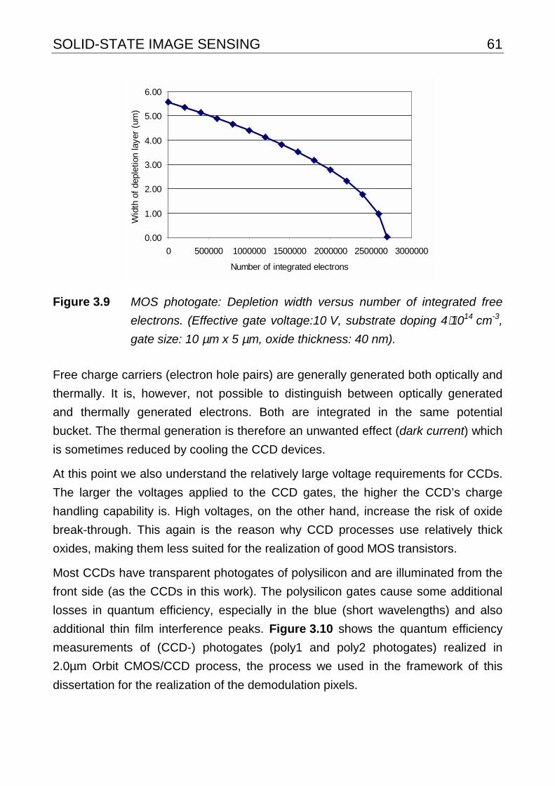
SOLID-STATE IMAGE SENSING 61
0.00
1.00
2.00
3.00
4.00
5.00
6.00
0 500000 1000000 1500000 2000000 2500000 3000000
Number of integrated electrons
Wid
th o
f de
plet
ion
laye
r (u
m)
Figure 3.9 MOS photogate: Depletion width versus number of integrated free
electrons. (Effective gate voltage:10 V, substrate doping 4⋅1014 cm-3,
gate size: 10 µm x 5 µm, oxide thickness: 40 nm).
Free charge carriers (electron hole pairs) are generally generated both optically and
thermally. It is, however, not possible to distinguish between optically generated
and thermally generated electrons. Both are integrated in the same potential
bucket. The thermal generation is therefore an unwanted effect (dark current) which
is sometimes reduced by cooling the CCD devices.
At this point we also understand the relatively large voltage requirements for CCDs.
The larger the voltages applied to the CCD gates, the higher the CCD’s charge
handling capability is. High voltages, on the other hand, increase the risk of oxide
break-through. This again is the reason why CCD processes use relatively thick
oxides, making them less suited for the realization of good MOS transistors.
Most CCDs have transparent photogates of polysilicon and are illuminated from the
front side (as the CCDs in this work). The polysilicon gates cause some additional
losses in quantum efficiency, especially in the blue (short wavelengths) and also
additional thin film interference peaks. Figure 3.10 shows the quantum efficiency
measurements of (CCD-) photogates (poly1 and poly2 photogates) realized in
2.0µm Orbit CMOS/CCD process, the process we used in the framework of this
dissertation for the realization of the demodulation pixels.
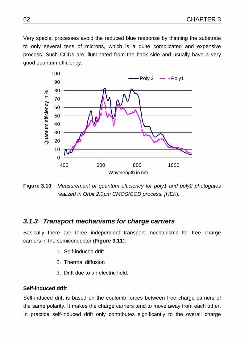
62 CHAPTER 3
Very special processes avoid the reduced blue response by thinning the substrate
to only several tens of microns, which is a quite complicated and expensive
process. Such CCDs are illuminated from the back side and usually have a very
good quantum efficiency.
0
10
20
30
40
50
60
70
80
90
100
400 600 800 1000
Wavelength in nm
Qu
an
tum
effi
cie
ncy
in %
Poly 2 Poly1
Figure 3.10 Measurement of quantum efficiency for poly1 and poly2 photogates
realized in Orbit 2.0µm CMOS/CCD process. [HEK].
3.1.3 Transport mechanisms for charge carriers
Basically there are three independent transport mechanisms for free charge
carriers in the semiconductor (Figure 3.11):
1. Self-induced drift
2. Thermal diffusion
3. Drift due to an electric field.
Self-induced drift
Self-induced drift is based on the coulomb forces between free charge carriers of
the same polarity. It makes the charge carriers tend to move away from each other.
In practice self-induced drift only contributes significantly to the overall charge
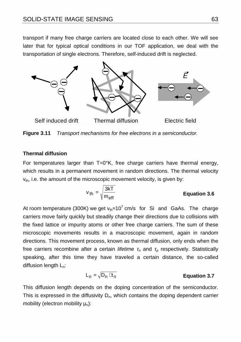
SOLID-STATE IMAGE SENSING 63
transport if many free charge carriers are located close to each other. We will see
later that for typical optical conditions in our TOF application, we deal with the
transportation of single electrons. Therefore, self-induced drift is neglected.
Self induced drift Thermal diffusion
E
Electric field
Figure 3.11 Transport mechanisms for free electrons in a semiconductor.
Thermal diffusion
For temperatures larger than T=0°K, free charge carriers have thermal energy,
which results in a permanent movement in random directions. The thermal velocity
vth, i.e. the amount of the microscopic movement velocity, is given by:
effth m
kT3v = Equation 3.6
At room temperature (300K) we get vth≈107 cm/s for Si and GaAs. The charge
carriers move fairly quickly but steadily change their directions due to collisions with
the fixed lattice or impurity atoms or other free charge carriers. The sum of these
microscopic movements results in a macroscopic movement, again in random
directions. This movement process, known as thermal diffusion, only ends when the
free carriers recombine after a certain lifetime τn and τp respectively. Statistically
speaking, after this time they have traveled a certain distance, the so-called
diffusion length Ln:
nnn DL τ⋅= Equation 3.7
This diffusion length depends on the doping concentration of the semiconductor.
This is expressed in the diffusivity Dn, which contains the doping dependent carrier
mobility (electron mobility µn):

64 CHAPTER 3
q
kTlv
3
1D ndiffthn ⋅µ=⋅⋅= Equation 3.8
Equivalently the electron needs a mean time tdiff to travel the distance ldiff by thermal
diffusion:
n
2diff
diff D
lt = Equation 3.9
In Equation 3.8 ldiff is the mean free path between collisions of the charge carrier
with the lattice or other carriers. Carrier diffusivity, mobility and lifetime depend on
the state of the charge carrier, whether they are the majority carriers or the minority
carriers. Generally, in photo elements, the minority carriers contribute to the
photocurrent and are therefore of interest. In the case of the p-type process we
used, electrons are the minority carriers. Therefore, we only gave the equations for
electron diffusivity and diffusion length above.
Figure 3.12 shows the dependency of mobility, lifetime and diffusion length as a
function of the doping concentration for both electrons and holes in silicon at
300° K.
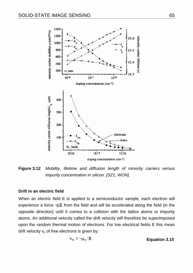
SOLID-STATE IMAGE SENSING 65
Figure 3.12 Mobility, lifetime and diffusion length of minority carriers versus
impurity concentration in silicon. [SZ1, WON].
Drift in an electric field
When an electric field E is applied to a semiconductor sample, each electron will
experience a force -q⋅E from the field and will be accelerated along the field (in the
opposite direction) until it comes to a collision with the lattice atoms or impurity
atoms. An additional velocity called the drift velocity will therefore be superimposed
upon the random thermal motion of electrons. For low electrical fields E this mean
drift velocity vn of free electrons is given by:
Ev nn ⋅µ−= Equation 3.10

66 CHAPTER 3
The proportionality factor between the electrical field and the drift velocity is the
carrier mobility µn (here electron mobility), given by:
eff
cn m
q τ⋅≡µ Equation 3.11
τ c is the mean free time, or the average time between collisions of the carriers with
the lattice or impurity atoms. It strongly depends on the semiconductor material, the
temperature and the doping concentration in the semiconductor (see also
Figure 3.12).
For very high electric fields this drift velocity approaches the thermal velocity, which
cannot be exceeded in silicon and thus defines the maximum drift velocity vmax (or
saturation velocity) in an electric field (107cm/s for Si) (see Figure 3.13):
effthmax m
kT3vv == Equation 3.12
Figure 3.13 Drift of free charge carriers in an electric field: saturation velocity.
[SZ2].
The correct expression for the drift velocity, considering the saturation velocity is:
max
n
nn
v
E1
Ev
⋅µ+
⋅µ= Equation 3.13
At this point it is worth mentioning two points:
(1) Generally, the carrier drift velocity in metal is much lower than in
semiconductors because of the lower mobility.
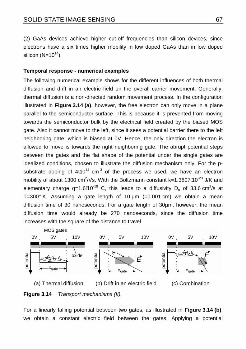
SOLID-STATE IMAGE SENSING 67
(2) GaAs devices achieve higher cut-off frequencies than silicon devices, since
electrons have a six times higher mobility in low doped GaAs than in low doped
silicon (N=1014).
Temporal response - numerical examples
The following numerical example shows for the different influences of both thermal
diffusion and drift in an electric field on the overall carrier movement. Generally,
thermal diffusion is a non-directed random movement process. In the configuration
illustrated in Figure 3.14 (a), however, the free electron can only move in a plane
parallel to the semiconductor surface. This is because it is prevented from moving
towards the semiconductor bulk by the electrical field created by the biased MOS
gate. Also it cannot move to the left, since it sees a potential barrier there to the left
neighboring gate, which is biased at 0V. Hence, the only direction the electron is
allowed to move is towards the right neighboring gate. The abrupt potential steps
between the gates and the flat shape of the potential under the single gates are
idealized conditions, chosen to illustrate the diffusion mechanism only. For the p-
substrate doping of 4⋅1014 cm-3 of the process we used, we have an electron
mobility of about 1300 cm2/Vs. With the Boltzmann constant k=1.3807⋅10-23 J/K and
elementary charge q=1.6⋅10-19 C, this leads to a diffusivity Dn of 33.6 cm2/s at
T=300° K. Assuming a gate length of 10 µm (=0.001 cm) we obtain a mean
diffusion time of 30 nanoseconds. For a gate length of 30µm, however, the mean
diffusion time would already be 270 nanoseconds, since the diffusion time
increases with the square of the distance to travel.
MOS gates
oxide
gatex
E
gatex
E
pote
ntia
l
pote
ntia
l
pote
ntia
l
0V 5V 10V 10V5V0V 0V 5V 10V
gatex
(a) Thermal diffusion (b) Drift in an electric field (c) Combination
Figure 3.14 Transport mechanisms (II).
For a linearly falling potential between two gates, as illustrated in Figure 3.14 (b),
we obtain a constant electric field between the gates. Applying a potential
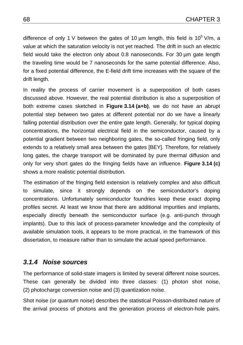
68 CHAPTER 3
difference of only 1 V between the gates of 10 µm length, this field is 105 V/m, a
value at which the saturation velocity is not yet reached. The drift in such an electric
field would take the electron only about 0.8 nanoseconds. For 30 µm gate length
the traveling time would be 7 nanoseconds for the same potential difference. Also,
for a fixed potential difference, the E-field drift time increases with the square of the
drift length.
In reality the process of carrier movement is a superposition of both cases
discussed above. However, the real potential distribution is also a superposition of
both extreme cases sketched in Figure 3.14 (a+b), we do not have an abrupt
potential step between two gates at different potential nor do we have a linearly
falling potential distribution over the entire gate length. Generally, for typical doping
concentrations, the horizontal electrical field in the semiconductor, caused by a
potential gradient between two neighboring gates, the so-called fringing field, only
extends to a relatively small area between the gates [BEY]. Therefore, for relatively
long gates, the charge transport will be dominated by pure thermal diffusion and
only for very short gates do the fringing fields have an influence. Figure 3.14 (c)
shows a more realistic potential distribution.
The estimation of the fringing field extension is relatively complex and also difficult
to simulate, since it strongly depends on the semiconductor’s doping
concentrations. Unfortunately semiconductor foundries keep these exact doping
profiles secret. At least we know that there are additional impurities and implants,
especially directly beneath the semiconductor surface (e.g. anti-punch through
implants). Due to this lack of process-parameter knowledge and the complexity of
available simulation tools, it appears to be more practical, in the framework of this
dissertation, to measure rather than to simulate the actual speed performance.
3.1.4 Noise sources
The performance of solid-state imagers is limited by several different noise sources.
These can generally be divided into three classes: (1) photon shot noise,
(2) photocharge conversion noise and (3) quantization noise.
Shot noise (or quantum noise) describes the statistical Poisson-distributed nature of
the arrival process of photons and the generation process of electron-hole pairs.
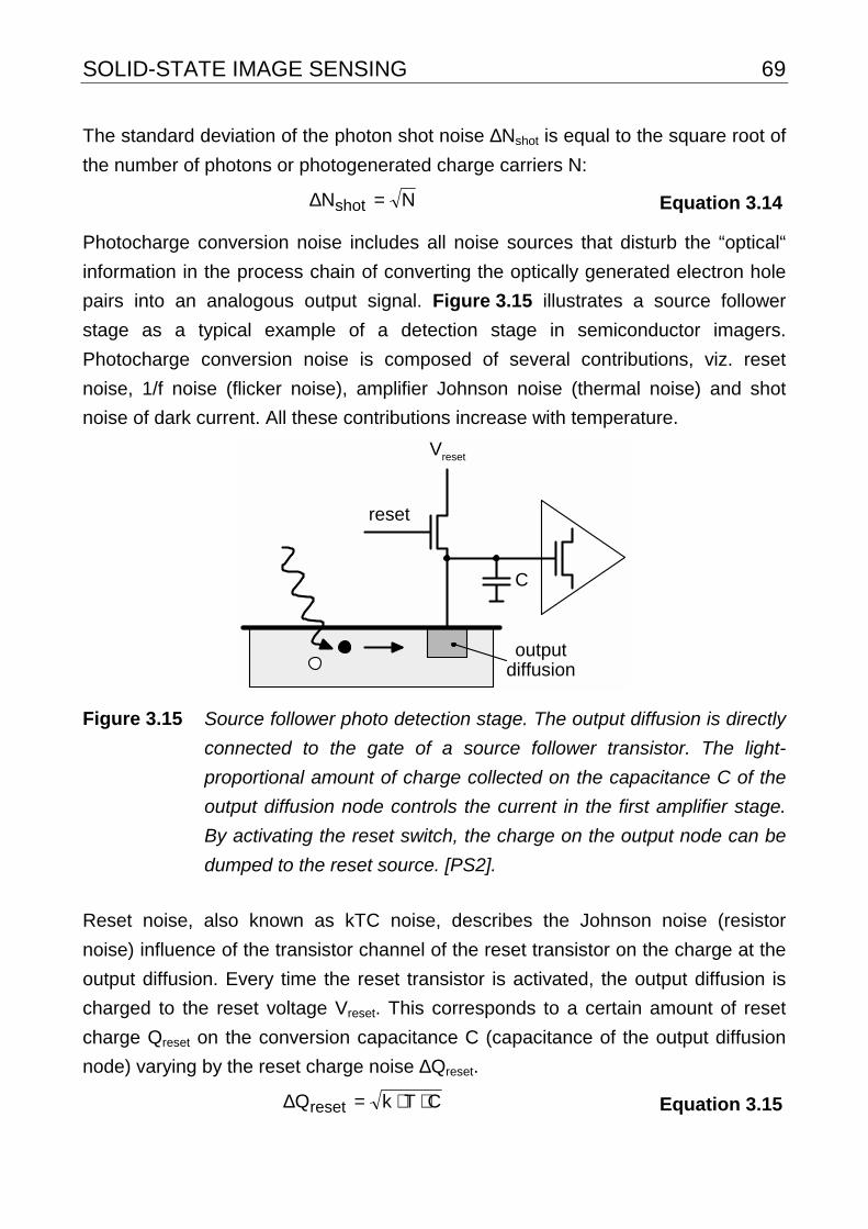
SOLID-STATE IMAGE SENSING 69
The standard deviation of the photon shot noise ∆Nshot is equal to the square root of
the number of photons or photogenerated charge carriers N:
NNshot =∆ Equation 3.14
Photocharge conversion noise includes all noise sources that disturb the “optical“
information in the process chain of converting the optically generated electron hole
pairs into an analogous output signal. Figure 3.15 illustrates a source follower
stage as a typical example of a detection stage in semiconductor imagers.
Photocharge conversion noise is composed of several contributions, viz. reset
noise, 1/f noise (flicker noise), amplifier Johnson noise (thermal noise) and shot
noise of dark current. All these contributions increase with temperature.
reset
Vreset
outputdiffusion
C
Figure 3.15 Source follower photo detection stage. The output diffusion is directly
connected to the gate of a source follower transistor. The light-
proportional amount of charge collected on the capacitance C of the
output diffusion node controls the current in the first amplifier stage.
By activating the reset switch, the charge on the output node can be
dumped to the reset source. [PS2].
Reset noise, also known as kTC noise, describes the Johnson noise (resistor
noise) influence of the transistor channel of the reset transistor on the charge at the
output diffusion. Every time the reset transistor is activated, the output diffusion is
charged to the reset voltage Vreset. This corresponds to a certain amount of reset
charge Qreset on the conversion capacitance C (capacitance of the output diffusion
node) varying by the reset charge noise ∆Qreset.
CTkQreset ⋅⋅=∆ Equation 3.15
70 CHAPTER 3
Flicker noise is caused by so-called semiconductor traps, which randomly capture
and release charge carriers, leading to statistical variations of the mobility and
concentration of free charge carriers in the transistor channel of the source follower
transistor [PS2]. Referred back to an input equivalent amount of charge, one
obtains the flicker noise contribution ∆Qflicker:
Bfg
fTk4CQ
sm
lkerflic ⋅
⋅⋅⋅⋅⋅=∆ Equation 3.16
where fl is the corner frequency, a process and layout dependent parameter, fs is
the sampling/ readout frequency, gm the transistor transconductance and B is the
bandwidth.
The noise equivalent input charge of the resistor noise in the channel of the source
follower transistor (Amplifier Johnson noise) is:
Bg
Tk4CQ
mamp ⋅α⋅⋅⋅⋅=∆ Equation 3.17
(α: 0.7..1, CMOS transistor parameter.)
Neglecting the amplification of the source follower output stage (usually about 0.8-
0.9) we can transform the above mentioned input noise out of the charge domain
into the equivalent output noise in the voltage domain:
Bg
Tk4V
Bfg
fTk4V
C
TkV
mamp
sm
lkerflic
reset
⋅α⋅⋅⋅=∆
⋅⋅
⋅⋅⋅=∆
⋅=∆
Equation 3.18
Dark current corresponds to the thermal generation of free electron hole pairs,
which competes with the optical generation and adds an offset charge to the
optically generated signal. Since thermally generated charge carriers are also
quantized, dark current adds an additional Poisson-distributed shot noise
contribution to the overall noise.
The sum of photocharge conversion noise can be drastically suppressed if the
sensor is operated at low temperatures (cooled imagers). With decreasing
minimum feature size of current and future semiconductor processes, lower

SOLID-STATE IMAGE SENSING 71
conversion capacitances C can be realized and that is one reason for steady
improvement of imager performances. These and many other additional clever
techniques (such as correlated double sampling) can be used to reduce
photocharge conversion noise.
Photon shot noise is a very important noise source, since it cannot be suppressed
and, therefore, is the ultimate theoretical limitation of all photo detectors. Also, since
photon shot noise increases with the amount of incoming photons, it finally
dominates all other noise sources and hence limits the effective signal-to-noise-
ratio for higher illumination levels. Figure 3.16 summarizes the above discussion.
Figure 3.16 Influence of single noise sources on the SNR. [TEU].
3.1.5 Sensitivity and Responsivity
The sensitivity s characterizes the conversion process of the optically generated
charge into an analogous output voltage. In essence it is determined by the size of
the conversion capacitance C and the amplification Asf of the output stage, in this
work, a two-stage source follower (C=40 fF and Asf=0.9). It is usually specified in
terms of volts per electron.
72 CHAPTER 3
⋅=electron
V q
C
As sf Equation 3.19
A small conversion capacitance C therefore leads to both low noise and high
sensitivity.
The responsivity r additionally takes into account the quantum efficiency of the
optical detection mechanism. It is expressed in terms of volts per photon and
depends on the wavelength of the light:
( ) ( )
⋅⋅λ=⋅λ=photon
V q
C
AQEsQEr sf Equation 3.20
3.1.6 Optical fill factor
The last important measure we would like to mention for solid-state photo-sensing
is the optical fill factor. This is the ratio of light sensitive pixel area to the total pixel
area. In APS sensors a certain amount of pixel area is occupied by the in-pixel
amplifier. Photons impinging on these areas do not in general contribute to the
optically generated signal. They are either reflected or absorbed by opaque metal
regions or they generate electron hole pairs, which are directly drained to a
diffusion. CMOS APS sensors have typical optical fill factors between 30% and
50%. In CCDs the optically generated charge is sometimes - depending on the
CCD architecture - stored in an opaque region of the pixel, also decreasing the
optical fill factor. CCDs usually have optical fill-factors between 50% and 100%.
For our TOF application a large optical fill factor is of essential importance since we
use active illumination. The optical power of the modulated illumination source is
both expensive and limited by eye-safety regulations. This requires the best
possible optical fill factor for an efficient use of the optical power and hence a high
measurement resolution.
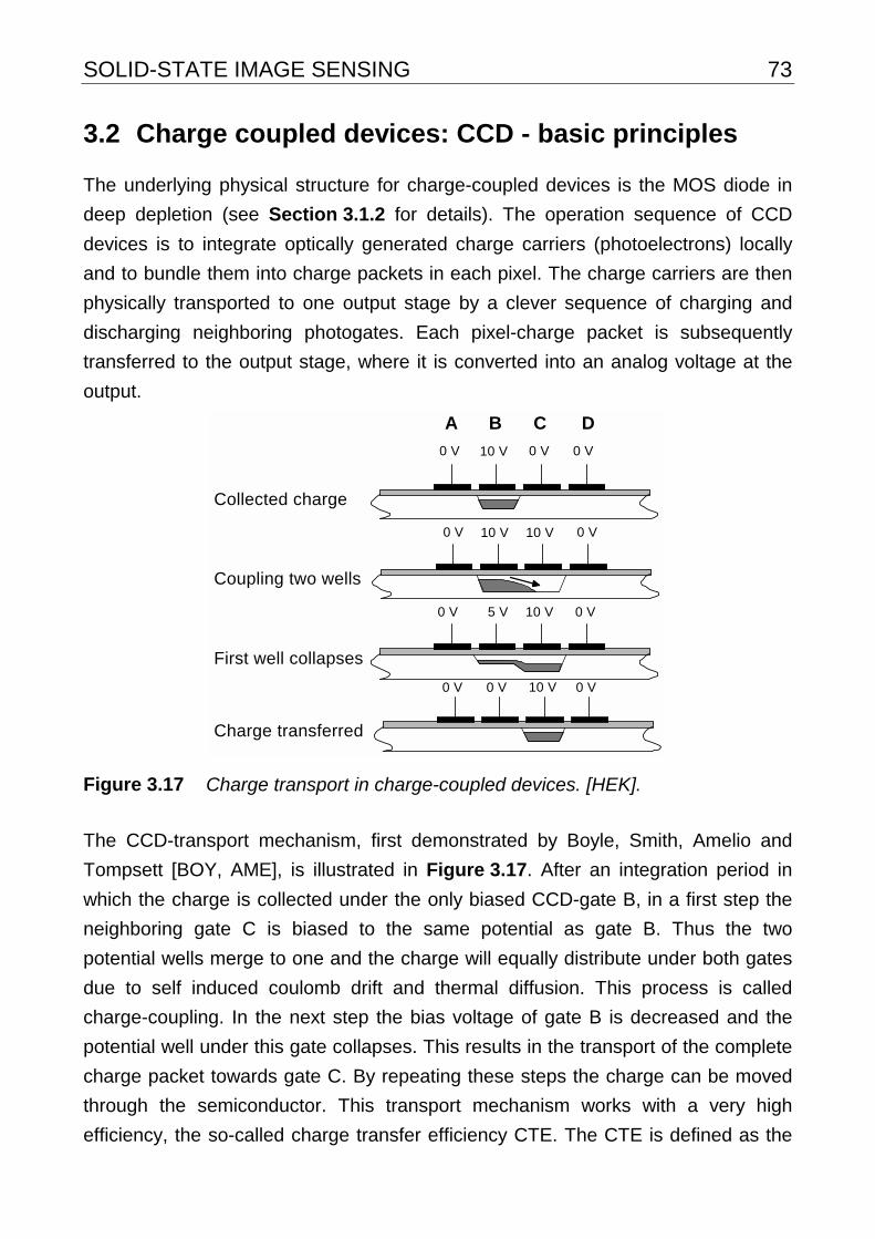
SOLID-STATE IMAGE SENSING 73
3.2 Charge coupled devices: CCD - basic principles
The underlying physical structure for charge-coupled devices is the MOS diode in
deep depletion (see Section 3.1.2 for details). The operation sequence of CCD
devices is to integrate optically generated charge carriers (photoelectrons) locally
and to bundle them into charge packets in each pixel. The charge carriers are then
physically transported to one output stage by a clever sequence of charging and
discharging neighboring photogates. Each pixel-charge packet is subsequently
transferred to the output stage, where it is converted into an analog voltage at the
output.
Collected charge
First well collapses
Charge transferred
Coupling two wells
0 V
10 V
0 V
0 V
10 V 10 V 0 V
0 V
10 V5 V 0 V
0 V
10 V
0 V
0 V0 V
A
B
C
D
Figure 3.17 Charge transport in charge-coupled devices. [HEK].
The CCD-transport mechanism, first demonstrated by Boyle, Smith, Amelio and
Tompsett [BOY, AME], is illustrated in Figure 3.17. After an integration period in
which the charge is collected under the only biased CCD-gate B, in a first step the
neighboring gate C is biased to the same potential as gate B. Thus the two
potential wells merge to one and the charge will equally distribute under both gates
due to self induced coulomb drift and thermal diffusion. This process is called
charge-coupling. In the next step the bias voltage of gate B is decreased and the
potential well under this gate collapses. This results in the transport of the complete
charge packet towards gate C. By repeating these steps the charge can be moved
through the semiconductor. This transport mechanism works with a very high
efficiency, the so-called charge transfer efficiency CTE. The CTE is defined as the
74 CHAPTER 3
amount of the charge packet that remains after the transport losses δ resulting from
the transport from one pixel to the next. One pixel mostly consists of three or four
CCD gates (three- / four-phase CCDs), however, also two-phase or even one-
phase CCDs have been reported (TEU).
( )δ−= 1CTE Equation 3.21
After transportation of the charge packet by N pixel positions, the following share of
the original charge remains:
( )NN 1CTE δ−= Equation 3.22
Typical CCD processes offer CTE values between 0.9999 and 0.99999. The
following table shows the influence of both CTE and number of charge transfers
(number of pixels) on the remaining charge packet.
CTE=0.99 CTE=0.999 CTE=0.9999 CTE=0.99999
N=10 90% 99% 99.9% 99.99%
N=100 37% 90% 99% 99.9%
N=1000 0% 37% 90% 99%
Remaining charge after N transfers for different CTE values.
The CCDs as we have described them so far are called surface channel CCDs
(SCCD). As can be seen in Figure 3.7 (b) the potential minimum in the vertical
direction for the classical MOS diode in deep depletion or strong inversion mode is
located directly at the junction between semiconductor and gate oxide. Since the
photoelectrons tend to stay at the potential minimum, the charge transport, which is
due to a superimposed potential difference in the horizontal direction, takes place at
the junction between semiconductor and oxide surfaces. Unfortunately, this junction
region is characterized by charge traps (caused by lattice mismatch, surface states
and impurities), which typically capture free electrons and randomly release them at
later times. This is one main technical limitation for a good CTE in SCCDs.
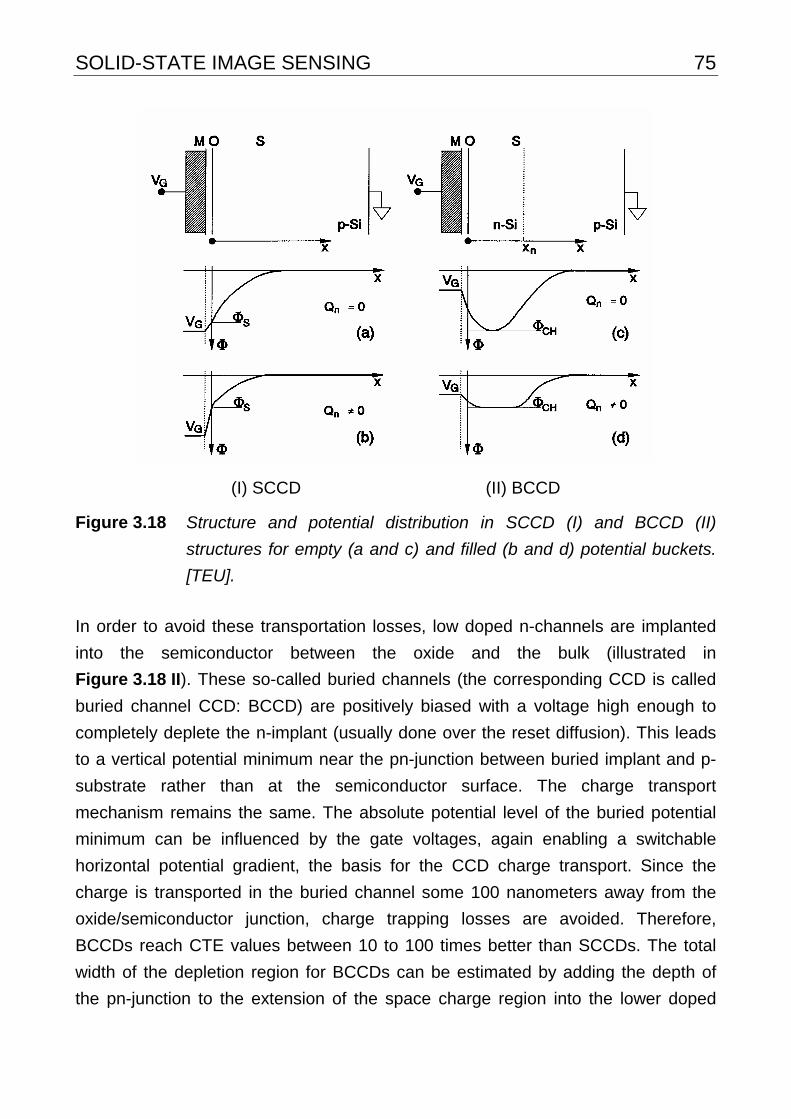
SOLID-STATE IMAGE SENSING 75
(I) SCCD (II) BCCD
Figure 3.18 Structure and potential distribution in SCCD (I) and BCCD (II)
structures for empty (a and c) and filled (b and d) potential buckets.
[TEU].
In order to avoid these transportation losses, low doped n-channels are implanted
into the semiconductor between the oxide and the bulk (illustrated in
Figure 3.18 II). These so-called buried channels (the corresponding CCD is called
buried channel CCD: BCCD) are positively biased with a voltage high enough to
completely deplete the n-implant (usually done over the reset diffusion). This leads
to a vertical potential minimum near the pn-junction between buried implant and p-
substrate rather than at the semiconductor surface. The charge transport
mechanism remains the same. The absolute potential level of the buried potential
minimum can be influenced by the gate voltages, again enabling a switchable
horizontal potential gradient, the basis for the CCD charge transport. Since the
charge is transported in the buried channel some 100 nanometers away from the
oxide/semiconductor junction, charge trapping losses are avoided. Therefore,
BCCDs reach CTE values between 10 to 100 times better than SCCDs. The total
width of the depletion region for BCCDs can be estimated by adding the depth of
the pn-junction to the extension of the space charge region into the lower doped
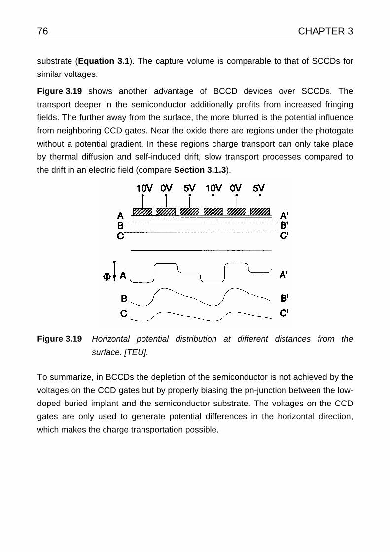
76 CHAPTER 3
substrate (Equation 3.1). The capture volume is comparable to that of SCCDs for
similar voltages.
Figure 3.19 shows another advantage of BCCD devices over SCCDs. The
transport deeper in the semiconductor additionally profits from increased fringing
fields. The further away from the surface, the more blurred is the potential influence
from neighboring CCD gates. Near the oxide there are regions under the photogate
without a potential gradient. In these regions charge transport can only take place
by thermal diffusion and self-induced drift, slow transport processes compared to
the drift in an electric field (compare Section 3.1.3).
Figure 3.19 Horizontal potential distribution at different distances from the
surface. [TEU].
To summarize, in BCCDs the depletion of the semiconductor is not achieved by the
voltages on the CCD gates but by properly biasing the pn-junction between the low-
doped buried implant and the semiconductor substrate. The voltages on the CCD
gates are only used to generate potential differences in the horizontal direction,
which makes the charge transportation possible.
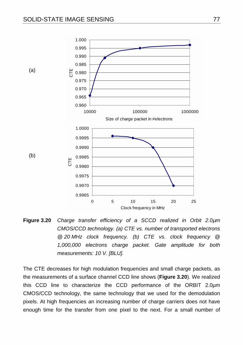
SOLID-STATE IMAGE SENSING 77
(a)
(b)
0.960
0.965
0.970
0.975
0.980
0.985
0.990
0.995
1.000
10000 100000 1000000
Size of charge packet in #electrons
CT
E
0.9965
0.9970
0.9975
0.9980
0.9985
0.9990
0.9995
1.0000
0 5 10 15 20 25
Clock frequency in MHz
CT
E
Figure 3.20 Charge transfer efficiency of a SCCD realized in Orbit 2.0µm
CMOS/CCD technology. (a) CTE vs. number of transported electrons
@ 20 MHz clock frequency. (b) CTE vs. clock frequency @
1,000,000 electrons charge packet. Gate amplitude for both
measurements: 10 V. [BLU].
The CTE decreases for high modulation frequencies and small charge packets, as
the measurements of a surface channel CCD line shows (Figure 3.20). We realized
this CCD line to characterize the CCD performance of the ORBIT 2.0µm
CMOS/CCD technology, the same technology that we used for the demodulation
pixels. At high frequencies an increasing number of charge carriers does not have
enough time for the transfer from one pixel to the next. For a small number of
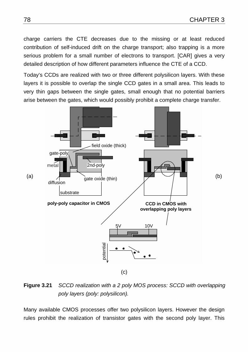
78 CHAPTER 3
charge carriers the CTE decreases due to the missing or at least reduced
contribution of self-induced drift on the charge transport; also trapping is a more
serious problem for a small number of electrons to transport. [CAR] gives a very
detailed description of how different parameters influence the CTE of a CCD.
Today’s CCDs are realized with two or three different polysilicon layers. With these
layers it is possible to overlap the single CCD gates in a small area. This leads to
very thin gaps between the single gates, small enough that no potential barriers
arise between the gates, which would possibly prohibit a complete charge transfer.
(a)
metal
field oxide (thick)
diffusiongate oxide (thin)
gate-poly
substrate
poly-poly capacitor in CMOS
2nd-poly
10V5V
po
ten
tial
CCD in CMOS with overlapping poly layers
(b)
(c)
Figure 3.21 SCCD realization with a 2 poly MOS process: SCCD with overlapping
poly layers (poly: polysilicon).
Many available CMOS processes offer two polysilicon layers. However the design
rules prohibit the realization of transistor gates with the second poly layer. This

SOLID-STATE IMAGE SENSING 79
could possibly cause gate breakthroughs. The second poly layer is offered only to
realize poly-poly capacitors only on top of the thick field oxide instead of the thinner
gate oxide. With a typical field oxide thickness of 0.6 µm (in contrast to 0.04 µm
gate oxide) the voltage on the polysilicon plate over the field oxide has nearly no
influence on the semiconductor potential. For this reason most CMOS processes
are not suitable for realizing CCDs with overlapping poly (see Figure 3.21 a). The
Orbit CMOS/CCD process allows the overlap of both poly layers over thin gate
oxide and thus enables the realization of surface channel CCDs with overlapping
polys (see Figure 3.21 b and c).
(a)
(b)
(c)
substrate
metal-wire
field oxide (thick)
diffusiongate oxide (thin)
poly gate
10V5V
gap too large, charge transport is not possible
po
ten
tial
10V5V
gap small enough, charge transport
is possible
po
ten
tial
Standard CMOS transistor (2 transistors in series)
Inter-poly gap CCD in CMOS (no diffusion between the gates)
(d)
(e)
(f)
Figure 3.22 SCCD realization with a one-poly MOS process:
Inter-poly-gap SCCD.
Generally, CCDs can also be realized in a technology with only one poly layer.
However, that the gap between two neighboring gates must be made small enough

80 CHAPTER 3
without causing short circuits. Actually, the first CCDs [BOY, AME] were produced
as one poly CCDs. Other successful implementations of CCDs with inter-poly gaps
are reported in [HOP], [FUR] and [KRA]. In most CMOS processes, however, it is
not possible to realize two neighboring gates without highly doped implant between
the gates (see Figure 3.22 a and b). Only a few processes offer special masks
(“non active implant” masks) to prohibit such a diffusion between the MOS gates
(Figure 3.22 d and e). Only if, additionally, the gap between the gates is small
enough (only a hundred to a few hundred nanometers) will the potential barrier
(Figure 3.22 c) disappear and a charge transfer become possible (Figure 3.22 f).
Today such CCDs with inter-poly gaps still require special processes but, with the
predictable future decrease in minimum feature size, sufficiently small inter-poly
gaps will become available and allows the implementation of CCDs with pure
CMOS processes. However, most of today’s CMOS processes only offer silicide
poly-layers for improved conductivity. Silicide gates are opaque and therefore not
suited for the realization of photogates.
The Orbit 2.0µm CMOS/CCD process additionally allows the realization of
overlapping polys over thin oxide, and hence makes possible the realization of
SCCDs. Also, as an option, a buried channel implant is available, which allows
BCCD realization. However, according to our measurements, the Orbit BCCDs are
only slightly better than the SCCDs. The Orbit 2.0µm CMOS/CCD process is
primarily a CMOS process, i.e. optimized for transistor structures rather than for
CCDs.
CCDs require relatively high control voltages to completely deplete the
semiconductor (in the case of SCCDs). Also the voltage amplitude defines the
charge-handling capability and hence the maximum signal amplitude (dynamic) that
the device can handle. Since many CCD gates are connected, the total gate
capacitance is often in the range of some nanofarads. Therefore, not only high
voltages but also high power is necessary to control CCD imagers, a serious
drawback for battery-powered systems. Charging and discharging the CCD gates
can require up to several amperes for some 10 MHz clocking speed.
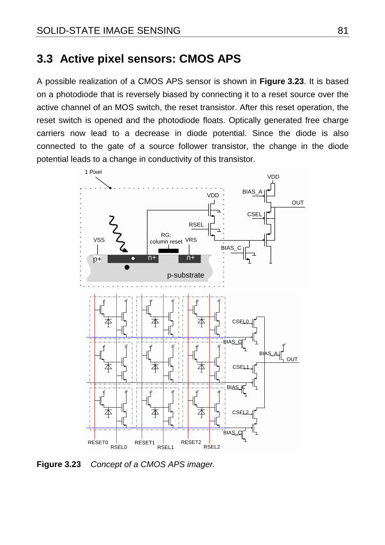
SOLID-STATE IMAGE SENSING 81
3.3 Active pixel sensors: CMOS APS
A possible realization of a CMOS APS sensor is shown in Figure 3.23. It is based
on a photodiode that is reversely biased by connecting it to a reset source over the
active channel of an MOS switch, the reset transistor. After this reset operation, the
reset switch is opened and the photodiode floats. Optically generated free charge
carriers now lead to a decrease in diode potential. Since the diode is also
connected to the gate of a source follower transistor, the change in the diode
potential leads to a change in conductivity of this transistor.
VSSRG:
column reset VRS
n+ n+
p-substrate
RSEL
VDD
1 Pixel
BIAS_C
VDD
CSEL
BIAS_A
OUT
p+
RSEL0RESET0
RSEL1RESET1
RSEL2RESET2
BIAS_C
CSEL2
BIAS_C
CSEL1
BIAS_C
CSEL0
OUTBIAS_A
Figure 3.23 Concept of a CMOS APS imager.

82 CHAPTER 3
Over an address decoder matrix each pixel can be accessed individually by
activating the corresponding row select and column select transistor switches. In
this way each in-pixel source follower transistor can selectively be switched into a
complete 2 stage source follower stage and change the output signal by it’s light
dependent conductivity.
CMOS APS, however, is not necessarily restricted to photodiodes; the light
sensitive areas could also be realized as photogates [FOS] or even some CCD
structures (see Chapter 5). APS only describes the principle of realizing active
pixels, that means pixels with an active stage (buffer transistor).
What has made CMOS APS a serious competitor on the imager market is above all
the (more or less) unmodified use of relatively cheap, widely available CMOS
processes. Not only are they available for prototyping services, enabling widely
spread research activity in this area, but they also benefit from the steady process
development driven by other industries (mainly computers).
For the customer, essential arguments for using CMOS sensors instead of CCD is
their low price, high functionality (digital cameras on a chip), low voltage (1.2V-5V)
and extremely low power consumption (20mW) [EMM]. Also they do not require
elaborate driving electronics but can be directly controlled by microcontroller, DSP
or FPGA logic.
SOLID-STATE IMAGE SENSING 83
3.4 Discussion
Both CCD and CMOS technologies are special MOS technologies. They differ in
optimizations of process parameters with different emphases. In a CCD line the
defect of a single CCD gate (oxide breakthrough) may make a complete column
unusable, whereas for CMOS APS only a single pixel would be unusable for a
comparable defect. CCDs therefore have thicker gate oxides and are characterized
by a certain process softness. In addition to the possibility of realizing overlapping
CCD gates for a barrier-free potential coupling in the semiconductor, today’s CCD
processes offer buried channel implants for enhanced CTE performance. Also the
substrate doping concentrations are usually lower than for CMOS processes,
leading to deeper depletion regions for the same gate voltages. Usually with CCD
processes only one type of transistor (p- or n-type) can be realized. Therefore only
limited electronics can be realized on-chip.
CMOS processes are optimized for fast reliable transistors with both n and p
channel. They are available in prototyping services - so called MPWs (Multi project
wafer). This allows the relatively cheap and uncomplicated realization of test
structures. Unfortunately such MPW services are not available for CCD processes.
Concerning this work, we would like to benefit from both the functionality of the
CCD principle (note: not necessarily CCD process) and the flexibility of CMOS
processes. As we will see in Chapter 5, we do not need CCD structures with a very
good CTE performance. This is because the demodulation principle only requires a
few charge transfers. The advantage of the CCD principle (also if realized in
CMOS) over CMOS circuitry is that it offers noise-free signal addition and defined
local and temporal charge separation, assuming proper CCD structures and timing.
In this way first signal processing steps (temporal sampling or demodulation in our
application) can already be realized in the pixel.

84 CHAPTER 3
Orbit’s 2.0µm CMOS/CCD process offers this possibility to realize both CCD and
CMOS structures. For our application it is not important to have the best CCD
performance as with pure CCD processes. A 2.0µm process is, however, coarse
compared to today’s CMOS processes (0.18µm), a clear indication that such a
process will probably not be supported for much longer. With future sub-micron
CMOS processes it will be possible to realize 1-poly surface channel CCDs with
sufficient transfer efficiency. This will open the door to the realization of further
signal processing tasks already in the pixel, using both the CCD principle and
CMOS circuitry, while maintaining reasonable fill factors.

POWER BUDGET AND RESOLUTION LIMITS 85
4. Power budget and resolution limits
Since the time-of-flight principle uses active illumination, it is important to know the
requirements for the optical power of the light source. For this purpose, two things
have to be known: (1) how much optical power of modulated scene illumination is
necessary to generate a given number of photoelectrons in one pixel and (2), how
many photoelectrons per sampling point and pixel are necessary to achieve a
certain range resolution? Both questions will be investigated and answered in this
chapter.
4.1 Optical power budget
The number of generated electrons is related to the number of photons over the
quantum efficiency of the imager. With the energy h⋅c/λ of one photon, the
integration time Tint, the size of the light sensitive pixel area Apix, and the size of the
image in the sensor plane Aimage, one can calculate the total amount of optical
power Pimage that must arrive at the sensor. Consideration of optical losses klens of
the lens and filters leads to the power Plens in front of the lens over the aperture
area. If the observed object is a Lambert reflector, one can calculate the optical
power on the observed scene, which has to be a factor of (D/2R)2 higher than the
power in front of the lens (D: aperture of the lens, R: distance to target). One
obtains the above factor by taking the ratio of the cosine-weighted (Lambert
reflection characteristics) integral over the spherical cap of diameter D, (i.e. the
share of optical power entering the lens), to the cosine-weighted integral over the
complete hemisphere (c.f. Equation 4.1, Figure 4.1).
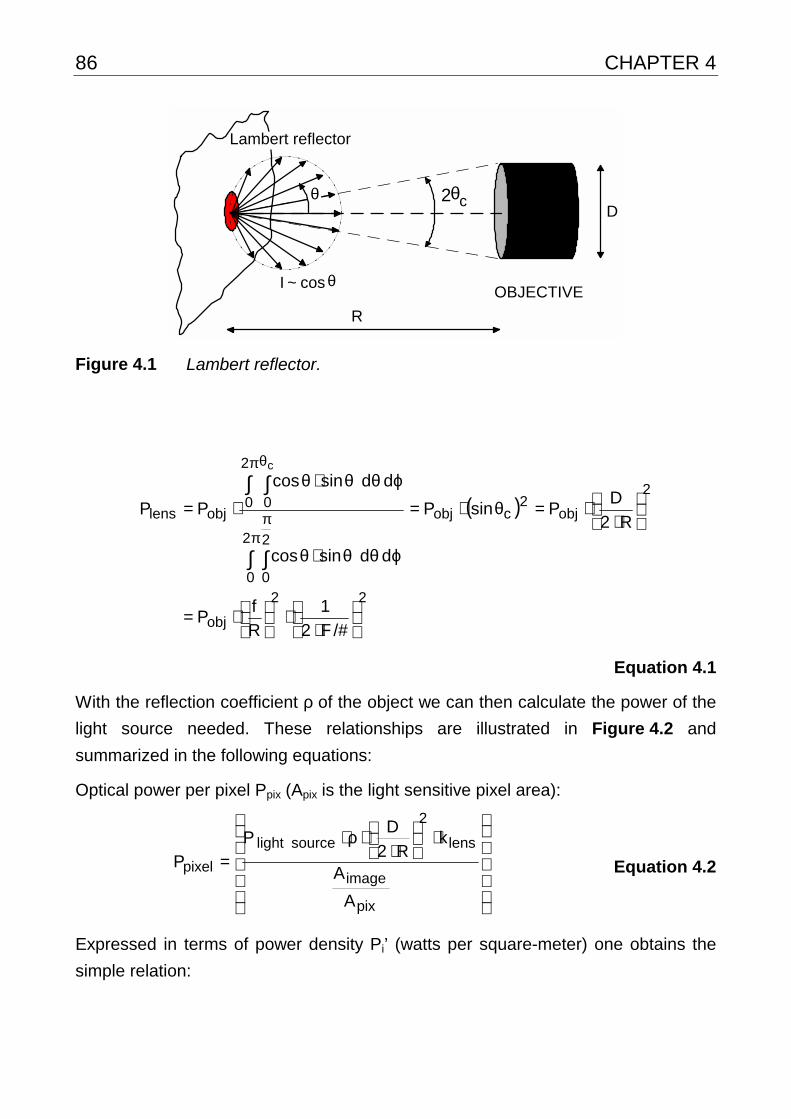
86 CHAPTER 4
OBJECTIVE
Lambert reflector
R
D
θcos~I
θ c2θ
Figure 4.1
Lambert reflector.
( )
22
obj
2
obj2
cobj
2
0
2
0
2
0 0objlens
/#F2
1
R
fP
R2
DPsinP
d d sincos
d d sincos
PP
c
⋅⋅
⋅=
⋅⋅=θ⋅=
ϕθθ⋅θ
ϕθθ⋅θ⋅=
∫ ∫
∫ ∫
ππ
πθ
Equation 4.1
With the reflection coefficient ρ of the object we can then calculate the power of the
light source needed. These relationships are illustrated in Figure 4.2 and
summarized in the following equations:
Optical power per pixel Ppix (Apix is the light sensitive pixel area):
⋅
⋅⋅ρ⋅
=
pix
image
lens
2
source light
pixel
A
A
kR2
DP
P Equation 4.2
Expressed in terms of power density Pi’ (watts per square-meter) one obtains the
simple relation:

POWER BUDGET AND RESOLUTION LIMITS 87
lens
2
objpixel k/#F2
1 'P'P ⋅
⋅⋅= Equation 4.3
# electrons
Plight source
required optical powerof light source
# photonsquantumefficiency
Epixel
energy per pixel
energy ofphoton
Ppixel
optical power on pixel
integration time
optical poweron sensor
pixel area,sensor area
Plens
optical power infront of lens
losses of lensand filter
Pobject
optical power on object(Lambert reflector)
distance of object,aperture of lens
Plight source
required opticalpower of light source
reflection coefficient of object
Pimage
Figure 4.2 Optical power budget: Strategy to estimate the optical power of the
illumination required to generate a given number of electrons in a
pixel as a function of scene and camera parameters.
Optical energy per pixel Epix:
intpixelpixel TPE ⋅= Equation 4.4
Number of photons Np per pixel:
ch
1TP
E
EN intpixel
photon
pixelp
λ⋅
⋅⋅== Equation 4.5
Number of electrons Ne generated per pixel (see also Figure 4.3):
)(QE
ch
1TP)(QENN intpixelpe λ⋅
λ⋅
⋅⋅=λ⋅= Equation 4.6
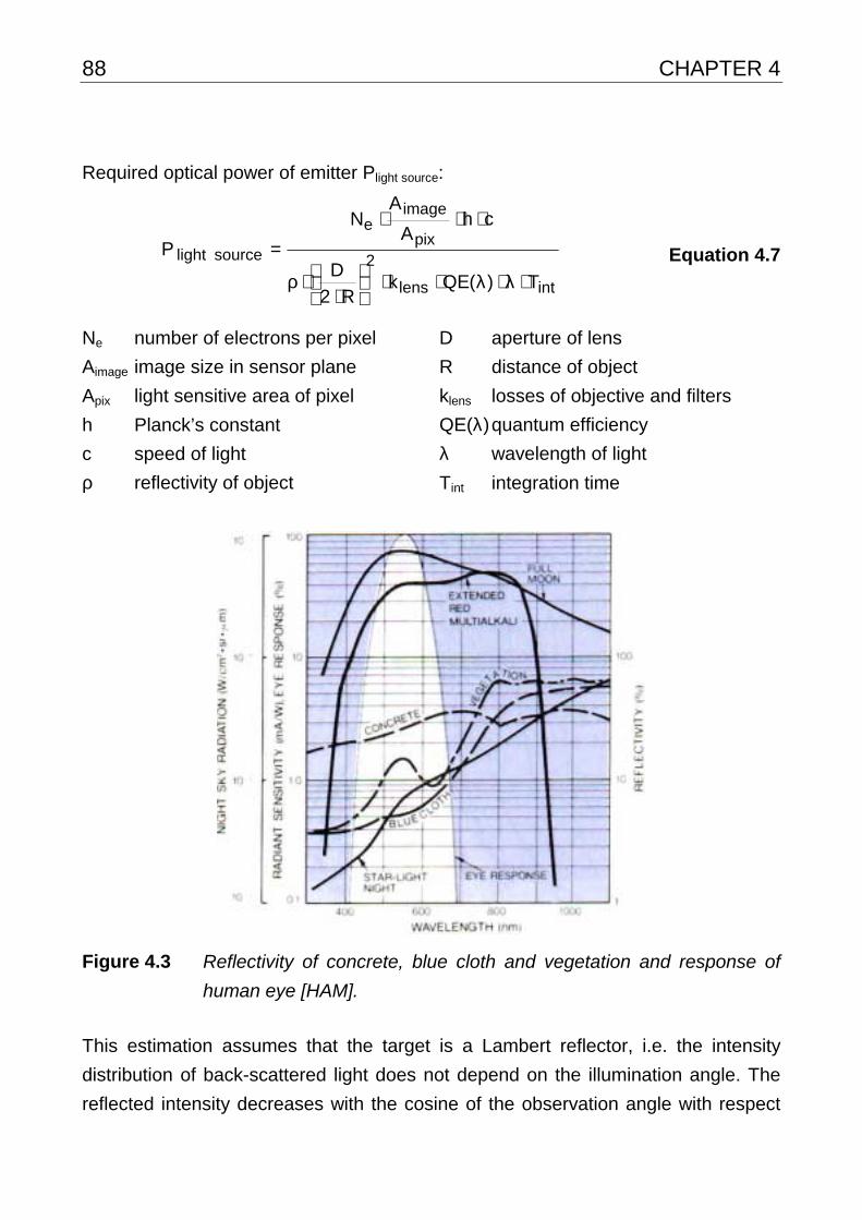
88 CHAPTER 4
Required optical power of emitter Plight source:
intlens
2pix
imagee
source light
T)(QEkR2
D
chA
AN
P
⋅λ⋅λ⋅⋅
⋅⋅ρ
⋅⋅⋅= Equation 4.7
Ne number of electrons per pixel
Aimage image size in sensor plane
Apix light sensitive area of pixel
h Planck’s constant
c speed of light
ρ reflectivity of object
D aperture of lens
R distance of object
klens losses of objective and filters
QE(λ) quantum efficiency
λ wavelength of light
Tint integration time
Figure 4.3 Reflectivity of concrete, blue cloth and vegetation and response of
human eye [HAM].
This estimation assumes that the target is a Lambert reflector, i.e. the intensity
distribution of back-scattered light does not depend on the illumination angle. The
reflected intensity decreases with the cosine of the observation angle with respect

POWER BUDGET AND RESOLUTION LIMITS 89
to the surface normal. The reflection coefficient has values between zero and one
for Lambert reflectors (ρ=1 for a white sheet of paper). Retro-reflectors, for example
in traffic signs, and mirrors lead to a directed reflection, which depends on the
illumination angle with respect to the surface normal. In the reflection direction the
equivalent reflectivity can then be larger than 1 (retro-reflector: ρ=100-1000, mirror:
ρ=1000). Figure 4.3 shows the wavelength dependent reflection coefficients of
concrete, vegetation and blue cloth. Table 4.1 gives an overview over reflectivity
values of typical diffusely reflecting materials at a wavelength of 900 nm.
White paper up to 100% Carbonate sand (dry) 57%
Snow 94% Carbonate sand (wet) 41%
White masonry 85% Rough clean wood pallet 25%
Limestone, clay up to 75% Smooth concrete 24%
Newspaper 69% Dry asphalt with pebbles 17%
Deciduous trees typ. 60% Black rubber tire 2%
Coniferous trees typ. 30%
Table 4.1 Typical reflectivity values for various materials [RIG].
It is interesting to note that a given optical power density on the object always leads
to the same number of electrons in the pixel, independent of its distance. If the
same light power is used to illuminate an area of one square meter, one 5 m away
from the sensor and another 50 m away from the sensor, the number of electrons
generated in one pixel stays the same. This is because the angle of view for the
observation of a fixed area also decreases with the distance of the object. Hence,
the illumination beam has to have a smaller divergence to illuminate the object at a
greater distance with the same power density. Put another way, with increasing
distance of the target, assuming that the power density on the target remains the
same, only the number of pixels illuminated by the target changes, not, however,
the power in each of the illuminated pixels (c.f. Equation 4.3).

90 CHAPTER 4
4.2 Noise limitation of range accuracy
In Chapter 3 we discussed the fact that the performance of solid state imagers is
limited by noise and that there are several different noise sources in both CCD
sensors and photodiode arrays. The essential ones are electronic and optical shot
noise, thermal noise, reset noise, 1/f noise and quantization noise. All of these
noise sources can be reduced or eliminated by different signal processing
techniques or cooling, except photon shot noise. Therefore, we first only investigate
the influence of shot noise on the ranging accuracy.
Quantum noise as final limitation
Shot noise describes the statistical Poisson-distributed nature of the arrival process
of photons and the generation process of electron-hole pairs. The standard
deviation of shot noise is equal to the square root of the number of photons (optical
shot noise) or photogenerated charge carriers (electronic shot noise). In the
following the required number of photoelectrons per sampling point and pixel to
achieve a given range resolution is derived.
As introduced in Chapter 2, the phase can be calculated from the sampling points
with the following equation (four-tap approach):
−−=ϕ
20
31AA
AAatan . Equation 4.8
Following the rules of error propagation
( ) ( ) ( ) ( )32
2
32
22
21
22
10
22
0A
AA
A A
AA
A∆⋅
∂
ϕ∂+∆⋅
∂
ϕ∂+∆⋅
∂
ϕ∂+∆⋅
∂
ϕ∂=ϕ∆
Equation 4.9
and considering that each of the integrated sampling points A0..A3 shows a standard deviation of ii AA =∆ , one obtains the quantum noise limited phase
error ∆ϕ:
3
2
32
2
21
2
10
2
0A
AA
AA
AA
A⋅
∂
ϕ∂+⋅
∂
ϕ∂+⋅
∂
ϕ∂+⋅
∂
ϕ∂=ϕ∆
. Equation 4.10

POWER BUDGET AND RESOLUTION LIMITS 91
Solving for special phase values (0°, 45°, 90°, 135°, 180°, …), and considering that
all sampling points are composed of an Offset B (background plus DC-component
of active illumination) and a phase-dependent component proportional to A⋅cos(ϕ0),
where A and B are given in number of electrons, we obtain the range resolution ∆L:
A2
B
8
L
360
LL
⋅⋅=ϕ∆⋅
°=∆ Equation 4.11
L: Non-ambiguity distance range (mod
modf2
c
2L
⋅=λ= ).
A: (De)modulation amplitude, i.e. the number of photoelectrons per pixel and
sampling point generated by the modulated light source. A depends on the
modulation depth of the modulated signal and the demodulation contrast of
the pixel (c.f. Section 5.2.2) but also on the optical power of the modulated
light source and the target’s distance and reflectivity.
B: Offset or acquired optical mean value, i.e. the number of photoelectrons per
pixel and sampling point generated by incoming light of the scene’s
background and the mean value of the received modulated light (c.f.
Figure 2.7).
This range accuracy (Equation 4.11), which can only be improved by averaging, is
the absolute limit of a lock-in range sensor working with four sampling points. One
can see from the equation that a large background brightness (B-A B for A<<B)
not only restricts the number of available quantization levels but also drastically
increases the quantum noise of the system. Background illumination can be
reduced by measuring in the dark or by using spectral filters that only transmit the
spectrum of the modulated light. Since, generally, the “active” optical power density
on the illuminated scene increases with decreasing distance to the object, the
ranging accuracy also increases for smaller distances. This is an important fact for
navigation applications, where a high accuracy is often only needed close to the
target.
Influence of thermal noise sources
Based on the above discussion, the additional noise sources (1/f- , reset- and
thermal noise) can easily be included in Equation 4.11 by adding an additional

92 CHAPTER 4
number of pseudo-background-electrons Npseudo to B. (They are not correlated to
the modulation signal and thus contribute to B rather than A.)
A2
NB
8
LL
pseudo
⋅
+⋅=∆ Equation 4.12
One obtains this number of pseudo-electrons Npseudo simply by squaring the noise-
equivalent number of noise electrons.
( )2
sf
convnoise dark2pseudo Aq
CVelectrons noise dark #N
⋅
⋅== Equation 4.13
Example: We assume a measured dark noise of Vdark noise=0.63 mV rms, containing
all noise sources except the photoelectron shot noise, namely the dark current shot
noise and the thermal noise floor. With a typical output amplification of Asf=0.9 and
a conversion capacitance of Cconv=40 fF this corresponds to an equivalent number
of 175 dark noise electrons, leading to 30,000 pseudo-background-electrons.
Vdark noise ≈ 0.63 mV rms
Asf ≈ 0.9
Cconv ≈ 40 fF
convsf
noise darkequivalent C
A
VQ ⋅= ≈ 2.8⋅10-17 C
q
Q electronsdark noise # equivalent= ≈ 175
Npseudo=(175)2 ≈ 30,000.
Demodulation amplitude and effective offset
A closer look at Equation 4.11 and Figure 2.7 shows that the modulated light
source contributes to both offset and demodulation amplitude. Integrated over a
certain integration time Tint, the mean optical power Popt,pixel directly adds a number
of photoelectrons PEopt to the effective offset Beff :
optpseudoeff PENbackgroundB ++= Equation 4.14
Also the number of demodulation-photoelectrons A can be expressed as a function
of the optical mean power or the total number of photoelectrons per pixel generated
by the modulated light source PEopt. Only the modulation contrast Cmod, a
parameter of the modulated light source, (usually 100%), and the demodulation

POWER BUDGET AND RESOLUTION LIMITS 93
contrast Cdemod, which depends on the pixel performance, (usually less than 100%),
have to be considered:
optdemodmod PECCA ⋅⋅= Equation 4.15
For 100% modulated optical signal we obtain:
optdemod PECA ⋅= Equation 4.16
Thus we can rewrite Equation 4.11:
optdemodmod
optpseudo
PECC2
PENbackground
8
LL
⋅⋅⋅
++⋅=∆ Equation 4.17
For the following example we assume a 100% modulated light source (Cmod=1) with
a total optical power of Popt=700 mW. The light source emits at 630 nm, where the
sensor has a quantum efficiency of 65%. We use a CS-mount lens with a focal
length of f=2.6 mm and a F/# of 1.0. The pixel size is 12.5 µm x 14.4 µm. With a
beam divergence of 50° (LED) we get an image size at the sensor plane of 4.6mm2
(2.6 mm * tan25°2⋅π). With optical losses of lens (0.7) and interference filter (0.5)
we obtain klens=0.35. Choosing an integration time of Tint=25 ms we can easily
calculate the number of electrons Ne generated in one pixel by rearranging
Equation 4.7:
2
pix
image
intlens2
source light e
R
1
chA
A4
T)(QEkDPN ⋅
⋅⋅⋅
⋅λ⋅λ⋅⋅⋅ρ⋅= Equation 4.18
Choosing a target with 20% reflectivity we get the number of electrons per pixel,
which now only depends on the distance R in meters (R/[m]):
Ne ≈ 170,000 photoelectrons / (R/[m])2. Hence, for a distance of 5 meters, we will
integrate a number of 34,000 electrons in one pixel. The following overview
summarizes the chosen parameters.

94 CHAPTER 4
Cmod = 1 QE(λ) = 0.65 klens = 0.35
Popt = 700 mW lens 1:1.0, 2.6 mm Tint = 25 ms
λ = 630 nm D = 2.6 mm ρ = 0.2
beam divergence = 50° Apixel = 180 µm2 Aimage = 4.6 mm2
Figure 4.4 to Figure 4.8 clarify the influence of the single parameters and give
numerical values for the range resolution that can be expected under certain
conditions.
Figure 4.4 shows both the received power and the number of generated electrons
per pixel depending on target distance and reflectivity. Figure 4.5 illustrates the
corresponding range resolution. In Figure 4.6 the demodulation contrast varies; this
was previously chosen as 40%. The influence of an additional background
illumination on the range resolution is shown in Figure 4.7.
Figure 4.8 plots the range resolution versus the optical power per pixel rather than
the distance in meters. Additionally the integration time varies. This figure is of
special importance. In Chapter 5 we present real range measurement values and
compare them to the prediction of Figure 4.8. We will demonstrate an excellent fit
between measurement and theory, which also confirms the predicted range
accuracies of Figure 4.5, Figure 4.6 and Figure 4.7.
Assuming an integration time of Tint = 25 ms, the modulation period of Tmod=50 ns,
which we choose for our TOF application (fmod=20 MHz, L=7.5 m), is a factor of
500,000 times shorter than Tint. Therefore, if a number of 50,000 photoelectrons
(c.f. Figure 4.4, light power: 700 mW) is generated in one pixel within the
integration time, only one photoelectron is collected every 10th modulation period
statistically speaking. Therefore, the demodulation pixels introduced in Chapter 5
will have to work with single photoelectrons, and at this point we understand, why
self-induced drift does not contribute to the charge transport in our application
(compare Chapter 3.1.3). According to Figure 4.8, the number of only 50,000
photoelectrons (1000 fW @ Tint=25 ms) leads to a range accuracy of about 2
centimeters.
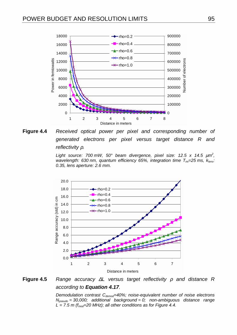
POWER BUDGET AND RESOLUTION LIMITS 95
0
2000
4000
6000
8000
10000
12000
14000
16000
18000
1 2 3 4 5 6 7 8Distance in meters
Po
we
r in
fem
tow
atts
0
100000
200000
300000
400000
500000
600000
700000
800000
900000
Nu
mb
er
of e
lect
ron
s
rho=0.2
rho=0.4
rho=0.6
rho=0.8
rho=1.0
Figure 4.4 Received optical power per pixel and corresponding number of
generated electrons per pixel versus target distance R and
reflectivity ρ.
Light source: 700 mW, 50° beam divergence, pixel size: 12.5 x 14.5 µm2, wavelength: 630 nm, quantum efficiency 65%, integration time Tint=25 ms, klens: 0.35, lens aperture: 2.6 mm.
0.0
2.0
4.0
6.0
8.0
10.0
12.0
14.0
16.0
18.0
20.0
1 2 3 4 5 6 7
Distance in meters
Ra
ng
e a
ccu
racy
(st
d)
in c
m
rho=0.2
rho=0.4
rho=0.6
rho=0.8
rho=1.0
Figure 4.5 Range accuracy ∆L versus target reflectivity ρ and distance R
according to Equation 4.17.
Demodulation contrast Cdemod=40%; noise-equivalent number of noise electrons Npseudo = 30,000; additional background = 0; non-ambiguous distance range L = 7.5 m (fmod=20 MHz); all other conditions as for Figure 4.4.
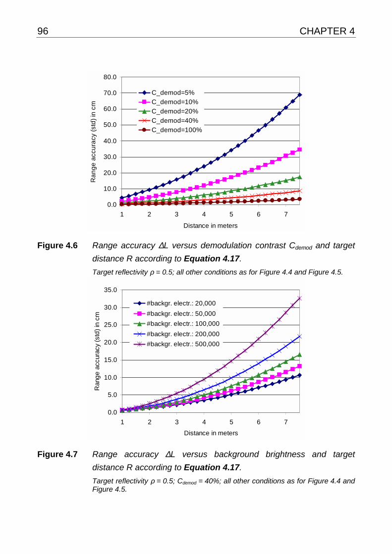
96 CHAPTER 4
0.0
10.0
20.0
30.0
40.0
50.0
60.0
70.0
80.0
1 2 3 4 5 6 7
Distance in meters
Ra
ng
e a
ccu
racy
(st
d)
in c
mC_demod=5%
C_demod=10%
C_demod=20%
C_demod=40%
C_demod=100%
Figure 4.6 Range accuracy ∆L versus demodulation contrast Cdemod and target
distance R according to Equation 4.17.
Target reflectivity ρ = 0.5; all other conditions as for Figure 4.4 and Figure 4.5.
0.0
5.0
10.0
15.0
20.0
25.0
30.0
35.0
1 2 3 4 5 6 7
Distance in meters
Ran
ge
acc
urac
y (s
td)
in c
m
#backgr. electr.: 20,000
#backgr. electr.: 50,000
#backgr. electr.: 100,000
#backgr. electr.: 200,000
#backgr. electr.: 500,000
Figure 4.7 Range accuracy ∆L versus background brightness and target
distance R according to Equation 4.17.
Target reflectivity ρ = 0.5; Cdemod = 40%; all other conditions as for Figure 4.4 and Figure 4.5.

POWER BUDGET AND RESOLUTION LIMITS 97
0 .00
5 .00
10 .00
15 .00
20 .00
25 .00
0 10 00 20 00 30 00 40 00 50 00
O p tic a l p o w e r in fe m to w atts
Ra
ng
e a
ccu
racy
(s
td)
in c
m
5 m s
12.5 m s
25 m s
In te g ra tio n tim e
Figure 4.8 Range accuracy ∆L versus optical input power per pixel and
integration time according to Equation 4.17.
Cdemod = 40%; all other conditions as for Figure 4.4 and Figure 4.5.

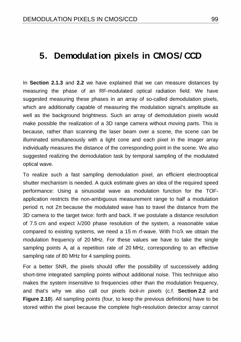
DEMODULATION PIXELS IN CMOS/CCD 99
5. Demodulation pixels in CMOS/CCD
In Section 2.1.3 and 2.2 we have explained that we can measure distances by
measuring the phase of an RF-modulated optical radiation field. We have
suggested measuring these phases in an array of so-called demodulation pixels,
which are additionally capable of measuring the modulation signal’s amplitude as
well as the background brightness. Such an array of demodulation pixels would
make possible the realization of a 3D range camera without moving parts. This is
because, rather than scanning the laser beam over a scene, the scene can be
illuminated simultaneously with a light cone and each pixel in the imager array
individually measures the distance of the corresponding point in the scene. We also
suggested realizing the demodulation task by temporal sampling of the modulated
optical wave.
To realize such a fast sampling demodulation pixel, an efficient electrooptical
shutter mechanism is needed. A quick estimate gives an idea of the required speed
performance: Using a sinusoidal wave as modulation function for the TOF-
application restricts the non-ambiguous measurement range to half a modulation
period π, not 2π because the modulated wave has to travel the distance from the
3D camera to the target twice: forth and back. If we postulate a distance resolution
of 7.5 cm and expect λ/200 phase resolution of the system, a reasonable value
compared to existing systems, we need a 15 m rf-wave. With f=c/λ we obtain the
modulation frequency of 20 MHz. For these values we have to take the single
sampling points Ai at a repetition rate of 20 MHz, corresponding to an effective
sampling rate of 80 MHz for 4 sampling points.
For a better SNR, the pixels should offer the possibility of successively adding
short-time integrated sampling points without additional noise. This technique also
makes the system insensitive to frequencies other than the modulation frequency,
and that’s why we also call our pixels lock-in pixels (c.f. Section 2.2 and
Figure 2.10). All sampling points (four, to keep the previous definitions) have to be
stored within the pixel because the complete high-resolution detector array cannot

100 CHAPTER 5
be read out at a frame rate of some tens of MHz. As the system uses active
illumination and the information of interest is carried by the modulated light, the fill
factor has to be as high as possible for good sensitivity (c.f. Chapter 3). Also the
dynamic range of the pixels is of high importance. The intensity of back-scattered
light decreases with the square of the target’s distance to the range camera (c.f.
Chapter 4). Another boundary condition for the pixel realization is that, due to a
limited research budget for this project, we only have access to semiconductor
technologies offered as MPWs (multi project wafers) that are more or less standard
processes. We can summarize the physical demands on our detector into four
principal tasks:
1. Energy conversion.
! Conversion of photons into electron-hole pairs.
2. Fast separation of optically generated charge carriers (photoelectrons).
! Avoidance of temporal blurring of the received time critical information.
3. Repeated, noise-free addition of separated photoelectrons.
! Improvement of SNR and insensitivity to spurious frequencies.
4. In-pixel storage of the acquired sampling points.
+
∑= i,00 aA
PIXEL
Energy conversion Fast Separation Repeated addition In-pixel storage
Figure 5.1 Physical demands on a demodulation pixel.
All these demands, illustrated in Figure 5.1, can be realized excellently with the
CCD principle. Better than any other electronic principle used in integrated circuits,
the CCD principle allows nearly loss-free addition and directed transport (spatial
distribution / shutter mechanism) of electrical signals in the charge domain.
DEMODULATION PIXELS IN CMOS/CCD 101
This chapter is divided into three main sections: In Section 5.1 we introduce
different realizations of demodulation pixels. They have all been realized in Orbit
2 µm CMOS/CCD technology, a process offered as MPW. This process has two
different polysilicon layers (poly1 and poly2) that can both be used as transistor
gates. Additionally the design rules allow these poly gates to overlap over the thin
gate oxide. Hence it is possible to realize CCDs with this CMOS/CCD process (c.f.
Section 3.2). The realized demodulation pixels vary in operational architecture,
maximum demodulation frequency and fill factor, the latter being a very important
parameter for realizing highly sensitive devices. All pixels fulfill the four physical
demodulation demands described above. The characteristic features of the pixels
introduced are summarized in Table 5.1 and Figure 5.8.
Section 5.2 then summarizes the results of a detailed characterization of the
demodulation performance for the 1-tap pixel, which is the pixel-realization with the
best electrooptical properties (demodulation bandwidth and optical fill factor). This
pixel has been fabricated twice; (1) with surface channel (SCCD) CCD structures
and (2) with buried channel (BCCD) structures, allowing a direct comparison of both
CCD types. Especially we focus on the efficiency of the shutter mechanism
(sampling efficiency or demodulation contrast) and its dependency on sampling
frequency and wavelength. Also, we present the measured phase accuracy as a
function of the optical power received in the pixel and compare these results to the
theory presented in Section 4.2. The 1-tap pixel is the basis for two lock-in sensor
arrays we realized, a line-sensor with 108 pixels and an image sensor with 64x25
pixels. Both arrays are implemented as range cameras, which are introduced in
Chapter 6.
Motivated by the outstanding results presented in Section 5.2, we present a very
simple and only slightly modified pixel structure in Section 5.3 that overcomes the
restrictions of the 1-tap pixel (serial integration of the single sampling points) by
offering two optically identical photosites.

102 CHAPTER 5
5.1 Pixel concepts
5.1.1 Multitap lock-in CCD
This device, introduced in [SP2] and [SP4], consists of a light sensitive photogate
that is connected to a 4-phase CCD-line, the pipeline-CCD. Every CCD-element,
consisting of four CCD gates, is connected to an identical CCD-line, the readout-
CCD, by so-called transfer gates (see Figure 5.2).
contact n+ diffusion poly 2 poly 1 light openingmetal wire CCD channel
Dimensions: photogate: 45x15 µm2, pixel: 45x270 µm2, aspect ratio: 1:6, fill factor: 5.6%.
a0 a1a2 a3
vertical transfer for charge addition in readout CCD
pote
ntia
l
PG DGdump diff.
CCD1CCD2
CCD3CCD4light shield
Figure 5.2 Multitap lock-in pixel: layout and cross-sectional view.
During the demodulation operation the upper CCD-line is clocked at maximum loss-
less speed so that photoelectrons from the photogate are transported into this CCD
line. With an appropriate choice of the modulation frequency (modulation period
equals the time of four CCD shifts) each CCD element within the pipeline CCD
carries one sampling point of the received modulated light after four CCD shifts. By
clocking the pipeline CCD, the temporal modulation is converted into spatial charge
distribution. This is the actual process of demodulation in the multitap-pixel. After
these four sampling points have been taken, they can be stored into the readout-
CCD by activating the transfer gates. During this transfer the additional
photoelectrons generated under the photogate can be dumped to a diffusion so that
DEMODULATION PIXELS IN CMOS/CCD 103
no parasitic charge will be integrated. This complete procedure can be repeated
until the amount of charge collected in the readout-CCD is large enough for a
sufficient SNR. Now the acquired sampling points can be transported to the
detection stage by clocking the readout-CCD. Each pixel has its own detection
stage (APS-concept, active pixel sensor) that can be selected for readout with an
address decoder.
A general problem in using CCD technology is the CCD’s speed performance. The
larger the length of a CCD gate, the longer the charge carriers need to travel from
this gate into the neighboring CCD gate. In Chapter 3 we have discussed that (1)
thermal diffusion, (2) self-induced drift (Coulomb forces) and (3) movement in an
electrical field (fringing field) are the only transport mechanisms for free charge
carriers in a semiconductor. Of these three the only directed and thus predictable
mechanism is the movement in a fringing field, the others being statistical
processes. Fringing fields, however, strongly depend on the semiconductor’s
impurity concentration, which is orders of magnitudes higher in the CMOS process
that we used than in a real CCD-process, used for commercial CCD sensors.
Therefore, in our CMOS-CCDs the fringing fields only extend to a very small region
between two adjacent gates. The transfer efficiency, only caused by thermal
diffusion, decreases with the square root of the gate length. This is why, for good
separation efficiency, the CCD gates have to be as short as possible, especially in
our CMOS/CCD process. For the same reason the size of the photogate may not
be chosen too large, otherwise the photoelectrons do not arrive in the pipeline-CCD
in time and the demodulation efficiency decreases. This limits the fill factor that can
be realized [CAR, SZ2].
In order to transfer charge-packets from the pipeline CCD into the readout CCD,
transfer gates had to be inserted between both CCD lines. Since only two poly-
layers are available and we have to follow special design rules, the insertion of
transfer gates forces the layout of relatively long gates in the pipeline CCD. This
stands in contradiction to our requirement for a high transport speed and a high fill
factor. The advantage of this pixel compared to other implementations is the
possibility of realizing any number of storage sites. For this reason we call it the
“multitap-approach”. It has been introduced as an 8-tap pixel in [SP2] but has also
been realized with 16 taps for a special application. A larger number of storage
sites offers the possibility of operating a TOF-ranger with more complex modulation
104 CHAPTER 5
signals as pseudo random noise. However, realizing a large number of in-pixel
storage sites is always a trade-off with the large fill factor desired.
The fill factor of the multitap-CCD pixel illustrated in Figure 5.2 is 5.6%, which is an
improvement of a factor 14 compared to the pixel originally introduced in [SP2].
This improvement was achieved (1) by reducing the number of storage sites from
8 to 4, (2) by using APS-readout and (3) by guiding the connecting metal wires
perpendicular to the CCD, which allows the realization of an enlarged photo-gate.
The multitap-CCD’s rectangular rather than square shape (aspect ratio of 1:6, if
realized with 4 taps) makes it poorly suited to be arranged in an array. Building a
line instead of a two-dimensional array improves the fill factor to 100%. However,
the long gates in the pipeline CCD only allow 4 MHz clocking frequency. That
corresponds to a maximum demodulation frequency of only 1 MHz using 4
sampling points per modulation period.
Summarizing, the multitap-pixel offers a flexible number of in-pixel storage sites.
With only 5.6% it has a poor fill factor. The large gate dimensions restrict the
demodulation frequency to 1 MHz, which is not fast enough for high-resolution
distance measurements in the range of 0-10 m.
5.1.2 4-tap lock-in pixel
Instead of connecting the photogate on only one side to a complete CCD line, as
described before, the 4-tap lock-in pixel follows a modified approach. The square
photogate is symmetrically connected to a transfer gate on each of its four sides.
These transfer gates can transport photoelectrons from the light sensitive
photogate into storage gates (see Figure 5.3). The demodulation process happens
immediately near the photo site. Only one CCD gate, the transfer gate, has to be
passed by the photoelectrons to reach the storage gate, where they can repetitively
be added over a large number of integration cycles. During demodulation operation
of the device the transfer gates are successively opened and closed synchronously
to the modulated input signal. With this mode of operation the input signal can be
rapidly sampled and the sampling points are stored in the storage gates. After this
accumulative demodulation process the sampling points can be read out.
DEMODULATION PIXELS IN CMOS/CCD 105
(a)
(b)
(c)
contact
n+ diffusion
poly 2
poly 1
light opening
metal wire
CCD channel
Dimensions: photogate: 15x15 µm2, pixel: 95x110 µm2, aspect ratio: 1:1,
fill factor: 2.2%.
contact n+ diffusionmetal wire
poly 2 poly 1 light opening
Dimensions: photogate: 15x15 µm2, pixel: 40x85 µm2, aspect ratio: 1:2,
fill factor: 6.6%.
a1 a3
pote
ntia
l
PGsamp1
store1 store3samp3
Figure 5.3 Four-tap lock-in pixel realized with (a) one- and (b) two output
diffusions: layout and cross-sectional view (c).
The 4-tap device has been realized in two different versions, one with a wheel-
shaped readout CCD, ending in only one sense diffusion node and one with two
separate sense diffusion nodes, doubling the conversion capacitance and thus
leading to only half the output voltage amplitude. The wheel-shaped CCD occupies
106 CHAPTER 5
a lot of space and diminishes the pixel’s fill factor to only 2.2%. In spite of the lower
conversion gain the 2-side readout version is the preferable realization of both 4-tap
pixels, because it offers a three times higher fill factor (6.6%) and has a reduced
demand on a highly efficient CCD charge transport. This is because the
photoelectrons only have to pass three CCD gates from their generation site, the
photogate, to the detection diffusion. The influences of the unconventionally shaped
CCD gates of both realization versions have to be investigated thoroughly.
The array-friendlier aspect ratio of 1:2 (1:1 respectively for the wheel-shaped
version) and the short transport paths of the photoelectrons in the demodulation
process are the major advantages of this 4-tap device compared to the multitap-
CCD. However, it is not possible to realize more than four storage sites with this
pixel architecture without drastically enlarging the photogate. The photogate, on the
other hand, should be as small as possible for a fast and efficient charge
separation. This appeared to be a problem in the first implementation of this
technique [SP1], where, due to an over-dimensioned size of the photogate
compared to the relatively narrow transfer gates, an inhomogeneous sensitivity of
the single sampling points could be measured. By the modified, highly symmetrical
pixel layouts shown in Figure 5.3 this problem of inhomogeneities between the
sampling points was partly overcome, at least for low sampling frequencies.
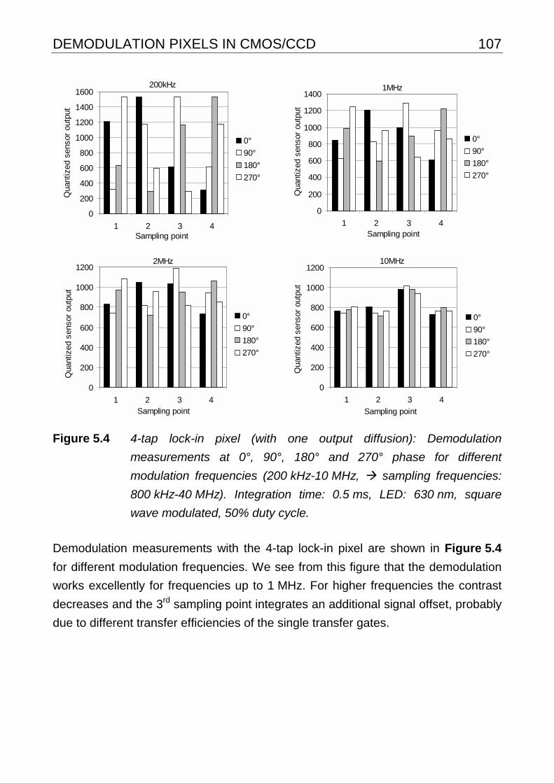
DEMODULATION PIXELS IN CMOS/CCD 107
200kHz
0
200
400
600
800
1000
1200
1400
1600
1 2 3 4Sampling point
Qua
ntiz
ed s
enso
r ou
tput
0°
90°
180°
270°
1MHz
0
200
400
600
800
1000
1200
1400
1 2 3 4Sampling point
Qua
ntiz
ed s
enso
r ou
tput
0°
90°
180°
270°
2MHz
0
200
400
600
800
1000
1200
1 2 3 4Sampling point
Qua
ntiz
ed s
enso
r ou
tput
0°
90°
180°
270°
10MHz
0
200
400
600
800
1000
1200
1 2 3 4
Sampling point
Qua
ntiz
ed s
enso
r ou
tput
0°
90°
180°
270°
Figure 5.4 4-tap lock-in pixel (with one output diffusion): Demodulation
measurements at 0°, 90°, 180° and 270° phase for different
modulation frequencies (200 kHz-10 MHz, ! sampling frequencies:
800 kHz-40 MHz). Integration time: 0.5 ms, LED: 630 nm, square
wave modulated, 50% duty cycle.
Demodulation measurements with the 4-tap lock-in pixel are shown in Figure 5.4
for different modulation frequencies. We see from this figure that the demodulation
works excellently for frequencies up to 1 MHz. For higher frequencies the contrast
decreases and the 3rd sampling point integrates an additional signal offset, probably
due to different transfer efficiencies of the single transfer gates.
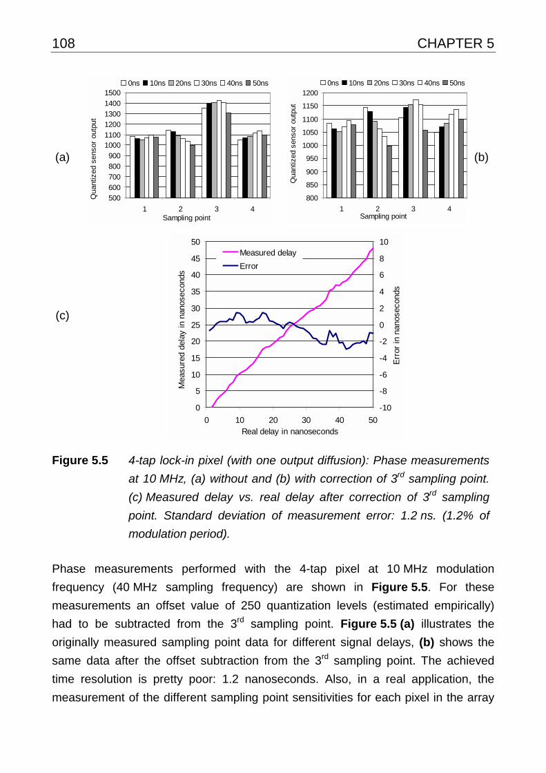
108 CHAPTER 5
(a)
500
600
700
800
900
10001100
1200
1300
1400
1500
1 2 3 4Sampling point
Qua
ntiz
ed s
enso
r ou
tput
0ns 10ns 20ns 30ns 40ns 50ns
800
850
900
950
1000
1050
1100
1150
1200
1 2 3 4Sampling point
Qua
ntiz
ed s
enso
r ou
tput
0ns 10ns 20ns 30ns 40ns 50ns
(b)
(c)
0
5
10
15
20
25
30
35
40
45
50
0 10 20 30 40 50Real delay in nanoseconds
Mea
sure
d de
lay
in n
anos
econ
ds
-10
-8
-6
-4
-2
0
2
4
6
8
10
Err
or in
nan
osec
onds
Measured delay
Error
Figure 5.5 4-tap lock-in pixel (with one output diffusion): Phase measurements
at 10 MHz, (a) without and (b) with correction of 3rd sampling point.
(c) Measured delay vs. real delay after correction of 3rd sampling
point. Standard deviation of measurement error: 1.2 ns. (1.2% of
modulation period).
Phase measurements performed with the 4-tap pixel at 10 MHz modulation
frequency (40 MHz sampling frequency) are shown in Figure 5.5. For these
measurements an offset value of 250 quantization levels (estimated empirically)
had to be subtracted from the 3rd sampling point. Figure 5.5 (a) illustrates the
originally measured sampling point data for different signal delays, (b) shows the
same data after the offset subtraction from the 3rd sampling point. The achieved
time resolution is pretty poor: 1.2 nanoseconds. Also, in a real application, the
measurement of the different sampling point sensitivities for each pixel in the array
DEMODULATION PIXELS IN CMOS/CCD 109
and the necessary correction of the measured data appear to be impractical.
Summarizing, the 4-tap pixel approach is only partly suited to range measurements,
since, for modulation frequencies higher than 1 MHz, it suffers from transfer
inhomogeneities between the single transfer gates.
5.1.3 1-tap lock-in pixel
Both pixel concepts introduced so far suffer from a low optical fill factor. In-pixel
storage always occupies space, in proportion to the number of sampling points to
be stored. The multitap approach only works up to 1MHz modulation frequency
(realized with 4 storage sites) because the demodulation process happens in the
extended area of a CCD line with design-rule-limited long CCD gates. The four-tap
lock-in pixel accesses the photogate with four different transfer gates, resulting in
an inhomogeneous response of the four sampling points. All of these limitations can
be traced back to the requirement of realizing four independent in-pixel storage
sites. The one-tap lock-in pixel ignores this requirement and offers only one storage
site but attempts to maximize the fill factor. Therefore, the sampling points have to
be stored externally.
Figure 5.6 shows the layout and a cross-sectional view (including the potential
distribution in the semiconductor) of the 1-tap pixel. The left and the right light
sensitive photogates (PGL and PGR) have a length of 6 µm, the middle photogate
a length of 2.5 µm; the pixel width is 21 µm. Each pixel also includes a reset
transistor, a source follower transistor (buffer amplifier) and the select transistor
(cascode with source follower). This leads to a pixel size of 65 µm by 21 µm and an
optical fill factor of more than 20%. The pixel’s working principle is illustrated in
Figure 5.7: By applying proper gate voltages to the photogates, the potential
gradient in the semiconductor can be influenced (c.f. Chapter 3). If the control
voltages of the photogates are changed synchronously with the modulated
incoming light, optically generated charge carriers can either be integrated (if they
belong to the sampling interval) or they are dumped to the dump diffusion (if they
do not belong to the sampling interval). This process can be repeated until the
integration gate (IG) has accumulated a sufficiently large signal. The addition or
accumulation of single electrons under the integration gate is essentially noise free.
This sampling mechanism is shown in Figure 5.7 (a), whereas (b) describes the
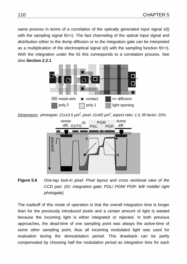
110 CHAPTER 5
same process in terms of a correlation of the optically generated input signal s(t)
with the sampling signal f(t+τ). The fast channeling of the optical input signal and
distribution either to the dump diffusion or to the integration gate can be interpreted
as a multiplication of the electrooptical signal s(t) with the sampling function f(t+τ).
With the integration under the IG this corresponds to a correlation process. See
also Section 2.2.1.
contact n+ diffusionmetal wire
poly 2 poly 1 light opening
Dimensions: photogate: 21x14.5 µm2, pixel: 21x65 µm2, aspect ratio: 1:3, fill factor: 22%.
pote
ntia
l
IGOUTG
sensediff. PGL
PGMPGR
dumpdiff.
Figure 5.6 One-tap lock-in pixel: Pixel layout and cross sectional view of the
CCD part. (IG: integration gate; PGL/ PGM/ PGR: left/ middle/ right
photogate).
The tradeoff of this mode of operation is that the overall integration time is longer
than for the previously introduced pixels and a certain amount of light is wasted
because the incoming light is either integrated or rejected. In both previous
approaches, the dead-time of one sampling point was always the active-time of
some other sampling point, thus all incoming modulated light was used for
evaluation during the demodulation period. This drawback can be partly
compensated by choosing half the modulation period as integration time for each
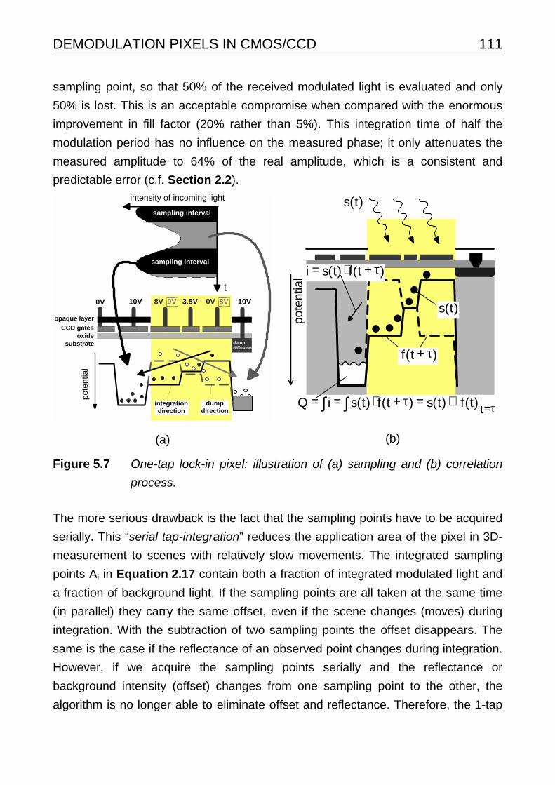
DEMODULATION PIXELS IN CMOS/CCD 111
sampling point, so that 50% of the received modulated light is evaluated and only
50% is lost. This is an acceptable compromise when compared with the enormous
improvement in fill factor (20% rather than 5%). This integration time of half the
modulation period has no influence on the measured phase; it only attenuates the
measured amplitude to 64% of the real amplitude, which is a consistent and
predictable error (c.f. Section 2.2).
dump direction
0V 10V 8V 3.5V 8V 10V0V 0V
oxideCCD gates
opaque layer
substrate
t
po
ten
tial
dumpdiffusion
intensity of incoming light
integrationdirection
sampling interval
sampling intervalsampling interval
(a)
po
ten
tial
)t(f τ+
)t(f)t(si τ+⋅=
τ=⊗=τ+⋅== ∫∫ t)t(f)t(s)t(f)t(siQ
)t(s
)t(s
(b)
Figure 5.7 One-tap lock-in pixel: illustration of (a) sampling and (b) correlation
process.
The more serious drawback is the fact that the sampling points have to be acquired
serially. This “serial tap-integration” reduces the application area of the pixel in 3D-
measurement to scenes with relatively slow movements. The integrated sampling
points Ai in Equation 2.17 contain both a fraction of integrated modulated light and
a fraction of background light. If the sampling points are all taken at the same time
(in parallel) they carry the same offset, even if the scene changes (moves) during
integration. With the subtraction of two sampling points the offset disappears. The
same is the case if the reflectance of an observed point changes during integration.
However, if we acquire the sampling points serially and the reflectance or
background intensity (offset) changes from one sampling point to the other, the
algorithm is no longer able to eliminate offset and reflectance. Therefore, the 1-tap
112 CHAPTER 5
device reacts very sensitively to such modulation of the scene that may be
superimposed on the temporal modulation. The good fill factor and the outstanding
demodulation performance and speed compensate this drawback by making short
integration times (only a few milliseconds) possible. For this reason the 1-tap
device is the most promising pixel-architecture for this 2.0 µm CMOS/CCD process.
Since all sampling points of one pixel are acquired with the same structure and
stored at the same storage site, this pixel has a highly uniform response for all
sampling points. The one side readout allows the photo site to be subdivided into
three short CCD gates. With these three gates a potential gradient of temporally
adjustable direction can be applied in the light sensitive region itself. Compared to
the 4-tap pixel, the transfer gates are implemented in the photogate itself, which is
now responsible for (1) optical generation, (2) fast separation and (3) repetitive
addition of photoelectrons. Therefore, by neglecting the task of in-pixel sampling
point storage, all demodulation requirements could be fulfilled in a small, completely
light sensitive spatial area giving the pixel an improved speed response and fill-
factor. Detailed measurements are presented in Section 5.2, an improved pixel
realization that overcomes the restriction of serial tap-integration is introduced in
Section 5.3.
This 1-tap device has been realized as a line sensor with 108 pixels and as an
array with 64 by 25 pixels. Both sensors are integrated in an all solid-state real-time
TOF range camera showing excellent performance (see Chapter 6).
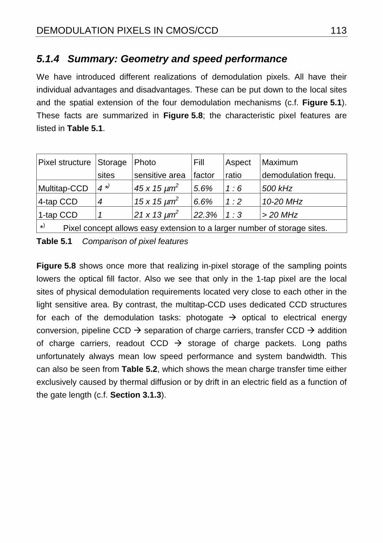
DEMODULATION PIXELS IN CMOS/CCD 113
5.1.4 Summary: Geometry and speed performance
We have introduced different realizations of demodulation pixels. All have their
individual advantages and disadvantages. These can be put down to the local sites
and the spatial extension of the four demodulation mechanisms (c.f. Figure 5.1).
These facts are summarized in Figure 5.8; the characteristic pixel features are
listed in Table 5.1.
Pixel structure Storage
sites
Photo
sensitive area
Fill
factor
Aspect
ratio
Maximum
demodulation frequ.
Multitap-CCD 4 *) 45 x 15 µm2 5.6% 1 : 6 500 kHz
4-tap CCD 4 15 x 15 µm2 6.6% 1 : 2 10-20 MHz
1-tap CCD 1 21 x 13 µm2 22.3% 1 : 3 > 20 MHz
*) Pixel concept allows easy extension to a larger number of storage sites.
Table 5.1 Comparison of pixel features
Figure 5.8 shows once more that realizing in-pixel storage of the sampling points
lowers the optical fill factor. Also we see that only in the 1-tap pixel are the local
sites of physical demodulation requirements located very close to each other in the
light sensitive area. By contrast, the multitap-CCD uses dedicated CCD structures
for each of the demodulation tasks: photogate ! optical to electrical energy
conversion, pipeline CCD ! separation of charge carriers, transfer CCD ! addition
of charge carriers, readout CCD ! storage of charge packets. Long paths
unfortunately always mean low speed performance and system bandwidth. This
can also be seen from Table 5.2, which shows the mean charge transfer time either
exclusively caused by thermal diffusion or by drift in an electric field as a function of
the gate length (c.f. Section 3.1.3).
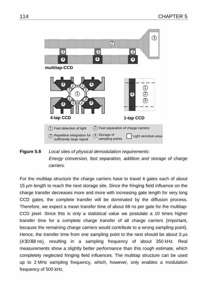
114 CHAPTER 5
Fast detection of light Fast separation of charge carriers
Repetitive integration for sufficiently large signal
Storage of sampling points
Light sensitive area3
1 2
4
12
4
3 3 3
44
multitap-CCD
4
44
4
3
33
32
2
22
1
4-tap CCD
24
1
3
1-tap CCD
Figure 5.8 Local sites of physical demodulation requirements:
Energy conversion, fast separation, addition and storage of charge
carriers.
For the multitap structure the charge carriers have to travel 4 gates each of about
15 µm length to reach the next storage site. Since the fringing field influence on the
charge transfer decreases more and more with increasing gate length for very long
CCD gates, the complete transfer will be dominated by the diffusion process.
Therefore, we expect a mean transfer time of about 68 ns per gate for the multitap-
CCD pixel. Since this is only a statistical value we postulate a 10 times higher
transfer time for a complete charge transfer of all charge carriers (important,
because the remaining charge carriers would contribute to a wrong sampling point).
Hence, the transfer time from one sampling point to the next should be about 3 µs
(4⋅10⋅68 ns), resulting in a sampling frequency of about 350 kHz. Real
measurements show a slightly better performance than this rough estimate, which
completely neglected fringing field influences. The multitap structure can be used
up to 2 MHz sampling frequency, which, however, only enables a modulation
frequency of 500 kHz.
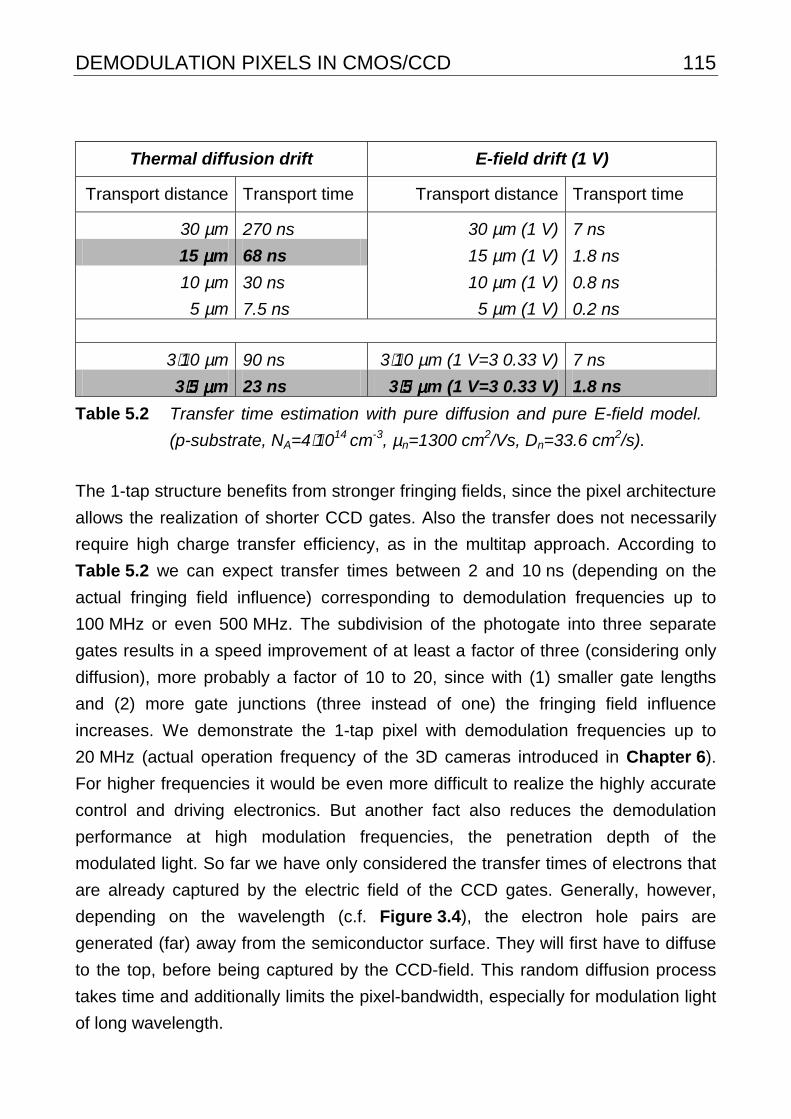
DEMODULATION PIXELS IN CMOS/CCD 115
Thermal diffusion drift E-field drift (1 V)
Transport distance Transport time Transport distance Transport time
30 µm 270 ns 30 µm (1 V) 7 ns
15 µµµµm 68 ns 15 µm (1 V) 1.8 ns
10 µm 30 ns 10 µm (1 V) 0.8 ns
5 µm 7.5 ns 5 µm (1 V) 0.2 ns
3⋅10 µm 90 ns 3⋅10 µm (1 V=3·0.33 V) 7 ns
3⋅⋅⋅⋅5 µµµµm 23 ns 3⋅⋅⋅⋅5 µµµµm (1 V=3·0.33 V) 1.8 ns
Table 5.2 Transfer time estimation with pure diffusion and pure E-field model.
(p-substrate, NA=4⋅1014 cm-3, µn=1300 cm2/Vs, Dn=33.6 cm2/s).
The 1-tap structure benefits from stronger fringing fields, since the pixel architecture
allows the realization of shorter CCD gates. Also the transfer does not necessarily
require high charge transfer efficiency, as in the multitap approach. According to
Table 5.2 we can expect transfer times between 2 and 10 ns (depending on the
actual fringing field influence) corresponding to demodulation frequencies up to
100 MHz or even 500 MHz. The subdivision of the photogate into three separate
gates results in a speed improvement of at least a factor of three (considering only
diffusion), more probably a factor of 10 to 20, since with (1) smaller gate lengths
and (2) more gate junctions (three instead of one) the fringing field influence
increases. We demonstrate the 1-tap pixel with demodulation frequencies up to
20 MHz (actual operation frequency of the 3D cameras introduced in Chapter 6).
For higher frequencies it would be even more difficult to realize the highly accurate
control and driving electronics. But another fact also reduces the demodulation
performance at high modulation frequencies, the penetration depth of the
modulated light. So far we have only considered the transfer times of electrons that
are already captured by the electric field of the CCD gates. Generally, however,
depending on the wavelength (c.f. Figure 3.4), the electron hole pairs are
generated (far) away from the semiconductor surface. They will first have to diffuse
to the top, before being captured by the CCD-field. This random diffusion process
takes time and additionally limits the pixel-bandwidth, especially for modulation light
of long wavelength.
116 CHAPTER 5
5.2 Characterization of 1-tap pixel performance
In this section, we present the characterization measurements for the 1-tap pixel. In
the first part we characterize the on-chip output stage (source follower) in terms of
sensitivity, linearity and saturation. Then we outline the motivation for the
measurements, describe the measurement setup and discuss the results to be
expected. With this knowledge, we present the measurements of demodulation
contrast and phase accuracy as a function of the control voltage amplitudes, the
modulation speed, the wavelength and the power of the modulated light. We also
present the results of noise measurements and compare the measured phase
accuracy with the prediction we presented in Section 4.2. We try to specify all
measurement parameters completely so that the measurements may be
reproduced. In order not to confuse the reader and to keep the measured data
clearly presented, we summarize some measurement details in the appendix
(coded as measurement conditions: MCDxyS for SCCD measurements and
MCDxyB for BCCD measurements).
The 1-tap pixel has been realized (1) as a linear array containing 108 pixels and (2)
as a 2D-array with 64 by 25 pixels. The line-sensor has been fabricated in two
technologies: as BCCD and as SCCD. The pixel characterizations have been
carried out with the line sensors. This offers the possibility to compare the buried
channel and surface channel CCD performance. More details of the overall sensor
architectures can be found in Chapter 6, where the camera implementations are
described.
5.2.1 Charge to voltage conversion
Sensitivity and Responsivity
The sensitivity is defined as the ratio of output voltage to input charge (unit:
Volt/electron). It is characterized by the output stage’s conversion capacitance and
amplification. Since, in our implementation, the input charge can only be generated
optically or thermally, it cannot be measured directly. So the sensitivity cannot really
be distinguished in isolation from the responsivity, which is the ratio of output
voltage to input light (unit: V/photon). The responsivity additionally contains the
quantum efficiency and therefore depends on the wavelength. None of the
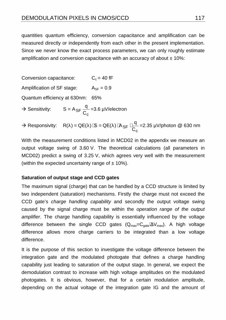
DEMODULATION PIXELS IN CMOS/CCD 117
quantities quantum efficiency, conversion capacitance and amplification can be
measured directly or independently from each other in the present implementation.
Since we never know the exact process parameters, we can only roughly estimate
amplification and conversion capacitance with an accuracy of about ± 10%:
Conversion capacitance: Cc = 40 fF
Amplification of SF stage: ASF = 0.9
Quantum efficiency at 630nm: 65%
! Sensitivity: c
SF C
qAS = =3.6 µV/electron
! Responsivity: c
SF C
qA)(QES)(QE)(R ⋅⋅λ=⋅λ=λ =2.35 µV/photon @ 630 nm
With the measurement conditions listed in MCD02 in the appendix we measure an
output voltage swing of 3.60 V. The theoretical calculations (all parameters in
MCD02) predict a swing of 3.25 V, which agrees very well with the measurement
(within the expected uncertainty range of ± 10%).
Saturation of output stage and CCD gates
The maximum signal (charge) that can be handled by a CCD structure is limited by
two independent (saturation) mechanisms. Firstly the charge must not exceed the
CCD gate’s charge handling capability and secondly the output voltage swing
caused by the signal charge must be within the operation range of the output
amplifier. The charge handling capability is essentially influenced by the voltage
difference between the single CCD gates (Qmax=Cgate⋅∆Vmax). A high voltage
difference allows more charge carriers to be integrated than a low voltage
difference.
It is the purpose of this section to investigate the voltage difference between the
integration gate and the modulated photogate that defines a charge handling
capability just leading to saturation of the output stage. In general, we expect the
demodulation contrast to increase with high voltage amplitudes on the modulated
photogates. It is obvious, however, that for a certain modulation amplitude,
depending on the actual voltage of the integration gate IG and the amount of
118 CHAPTER 5
charge already integrated, it will be possible for charge carriers integrated under IG
to be transported back into the light sensitive pixel area and to be dumped to the
dump diffusion. The maximum charge to be integrated within the pixel is defined by
the output stage. The conversion capacitance of 40 fF, together with the
amplification of 0.9 and a maximum output voltage swing of 4 V, leads to a
maximum number of about 1,100,000 electrons that can be integrated without
causing signal clipping due to saturation of the output stage.
To determine the charge that leads to saturation of the output stage, we bias the
gates PGM and PGR with 10 V (so that they are definitely at a higher potential than
PGL) and use PGL as a variable barrier. In this way the potential difference
between PGL and IG adjusts the amount of charge that IG can hold (c.f.
Figure 5.9). The integration gate IG is always biased at 10.7 V, a reliable amplitude
that avoids device damage by oxide break through. The illumination time is chosen
to be long enough that the potential well, generated by the potential difference
between IG and PGL, is always totally filled. Additionally generated charge carriers
can no longer be held by IG.
As the result of this measurement we find that a potential-difference of 2.2 V
between IG and PGL defines the full-well charge that leads to saturation of the
output stage (IG=10.7 V, PGL=8.5 V). For lower PGL voltages (e.g. 8 V) the output
signal does not increase further, because the amount of charge that will be
integrated then leads to saturation of the output stage. For higher PGL voltages
(e.g. 9 V), the output signal decreases, because the full-well charge is smaller than
the maximum charge that the output stage can handle. Therefore, the amplitude of
PGL should not exceed 8.5 V for the demodulation application (assuming
IG = 10.7 V). Otherwise, the maximum signal that can be handled is no longer
limited by the output stage but by the actual potential difference between IG and
PGL.
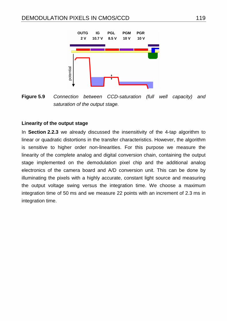
DEMODULATION PIXELS IN CMOS/CCD 119
pote
ntia
l
10.7 V 8.5 V 10 V 10 V
IG PGL PGM PGR
2 V
OUTG
Figure 5.9 Connection between CCD-saturation (full well capacity) and
saturation of the output stage.
Linearity of the output stage
In Section 2.2.3 we already discussed the insensitivity of the 4-tap algorithm to
linear or quadratic distortions in the transfer characteristics. However, the algorithm
is sensitive to higher order non-linearities. For this purpose we measure the
linearity of the complete analog and digital conversion chain, containing the output
stage implemented on the demodulation pixel chip and the additional analog
electronics of the camera board and A/D conversion unit. This can be done by
illuminating the pixels with a highly accurate, constant light source and measuring
the output voltage swing versus the integration time. We choose a maximum
integration time of 50 ms and we measure 22 points with an increment of 2.3 ms in
integration time.

120 CHAPTER 5
0 5 10 15 20 250
500
1000
1500
2000
2500
3000
3500
4000 Linearity measurement (I): FS46
BRIGHT measurement
0 5 10 15 20 250
50
100
150
200
250 Linearity measurement (II): FS46
DARK measurement
Figure 5.10 Linearity measurements of the output stage for different illumination
intensities and integration times (0-50 ms).
The measurement (Figure 5.10) is performed for two illumination intensities, one
nearly leading to saturation of the output stage for the longest integration time
(BRIGHT measurement) and the other with a factor of 100 lower intensity (DARK
measurement). The measurement conditions chosen are summarized in MCD01 in
the appendix. For the quantization of the analog output, we use the EPPI
(Enhanced Parallel Port Interface, a CSEM product), a 12 bit frame grabber that
can be connected to the parallel port of a PC.
We can already judge by eye that the overall system linearity appears to be good
(Figure 5.10). Only for very low output voltages (DARK measurement) does the
linearity deteriorate. To judge the actual influence of this DARK measurement
nonlinearity, we approximate the measured curve with a polynomial. This can easily
be done with MATLAB (polynom: 432 x0003.0x02.0x53.0x2.13 ⋅−⋅+⋅−⋅ , for
0<x<22). With the knowledge of this nonlinearity, the resulting phase error for the
range measurement application can be estimated (as in Section 2.2.2). We find
that the maximum phase error caused by the actual measured nonlinearities of our
system is less than ± 0.5 degrees. Hence, the linearity of our output transistor and
A/D conversion chain is sufficient for the targeted range imaging application.
5.2.2 Measurement setup, expectations and predictions
Before we present the measurements for the 1-tap pixel in Sections 5.2.3 - 5.2.8 we
will first outline the motivation and describe these measurements. In this section,
DEMODULATION PIXELS IN CMOS/CCD 121
we describe the measurements that we will perform later and the setup that we use
for these measurements. In addition, we will make predictions about how the pixel
performance will change as a function of different parameters.
What is “demodulation contrast”?
We already discussed in Section 4.2 that, for a good phase accuracy, not only the
contrast (or modulation depth) of the modulated light source but also the shutter
efficiency is of essential importance. Both define the measured contrast, which
directly influences the ranging accuracy (c.f. Equation 4.10). In optics the
modulation is defined as follows:
minmax
minmax
II
IImodulation
+−
=
Equation 5.1
Similarly, we define the demodulation contrast Cdemod as:
offset measured
amplitude measuredC modde =
Equation 5.2
There are several parameters attenuating the measured amplitude. In Chapter 2
we mentioned that the integrative acquisition process of the sampling points Ai
leads to a decrease in measured amplitude (c.f. Equation 2.18). For the distance
measurement, we operate the lock-in sensor at a modulation frequency of 20 MHz
with a sampling interval of 25 ns. Thus, the integration time for the sampling point
acquisition is half the modulation period. Therefore, according to Figure 2.7, the
measured amplitude is only 64% of the real amplitude. In addition to this more
system theoretical amplitude attenuation, there are also physical effects (shutter
inefficiency) that lower the measured amplitude and increase the measured offset.
The demodulation contrast quantifies the CCD’s (im)perfection of charge
separation. It should be as high as possible in order to achieve large signal
amplitude and hence a good signal-to-noise ratio for the phase detection. The
shutter efficiency depends on the following parameters:
• Demodulation frequency: The higher the demodulation frequency (or sampling
frequency) the shorter is the time available for the single charge carriers to travel
122 CHAPTER 5
from their site of optical generation to the storage area. If they do not reach the
right storage site in time, they will contribute to a wrong sampling point and lower
the demodulation amplitude.
• Fringing fields: The higher the fringing fields between two adjacent electrodes
the higher is the speed of charge transfer and thus the resulting demodulation
efficiency increases, especially at high frequencies.
• Gate length: The smaller the gate length the more quickly the photoelectrons
arrive at the storage sites and the higher becomes the influence of fringing
fields. A small gate length is therefore the key parameter for a fast demodulation
performance.
• Wavelength: The use of long wavelength light leads to a large penetration depth
of the incident light. This again causes long diffusion times and blurred diffusion
directions. The effective charge capturing area grows. This reduces the
sharpness (crosstalk) and leads to a lower demodulation contrast. Long diffusion
times lower the demodulation cut-off frequency, while the blurring effect (also
opaque CCD gates directly collect photogenerated charge) also appears at low
modulation frequencies or even under DC conditions.
Optical measurement setup
Figure 5.11 shows the optical test setup for the measurements described below.
The lock-in sensor chip is mounted on the camera board, which is fixed to an XY-
table under a microscope. This microscope is used to illuminate the chip with a
variable amount of optical power. LEDs of different wavelength are used to
illuminate the pixels. They can be plugged into a fast LED driver module (MV-LED1
[CS1]), which is capable of modulating them up to 20 MHz, depending on their
internal capacitances.
The light of the LED passes through an iris (or pinhole) and the objective of the
microscope. The distance from the objective to the lock-in chip is adjusted such that
the light beam is not in focus on the chip. In this way we get a homogenous light
spot on top of the chip, leading to an equal illumination of all the pixels. By varying
the distance of the objective to the chip we can adjust the size of the light spot and,
hence, the illumination intensity on the chip. By measuring the total power of the
light spot and the diameter of the spot, the total optical power on the photogate can
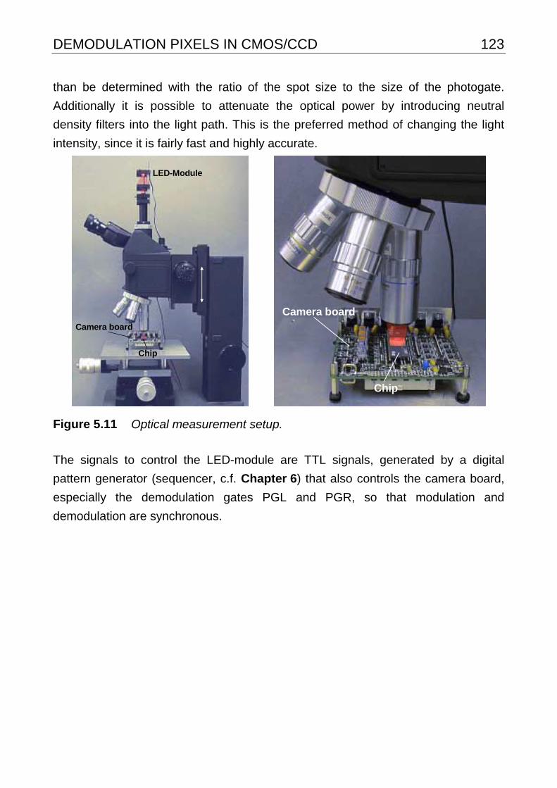
DEMODULATION PIXELS IN CMOS/CCD 123
than be determined with the ratio of the spot size to the size of the photogate.
Additionally it is possible to attenuate the optical power by introducing neutral
density filters into the light path. This is the preferred method of changing the light
intensity, since it is fairly fast and highly accurate.
LED-Module
Camera board
Chip
Camera board
Chip
Figure 5.11 Optical measurement setup.
The signals to control the LED-module are TTL signals, generated by a digital
pattern generator (sequencer, c.f. Chapter 6) that also controls the camera board,
especially the demodulation gates PGL and PGR, so that modulation and
demodulation are synchronous.
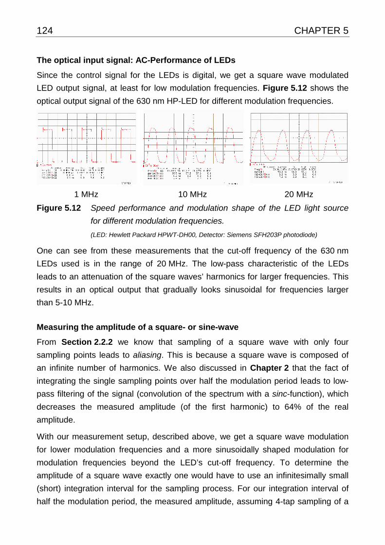
124 CHAPTER 5
The optical input signal: AC-Performance of LEDs
Since the control signal for the LEDs is digital, we get a square wave modulated
LED output signal, at least for low modulation frequencies. Figure 5.12 shows the
optical output signal of the 630 nm HP-LED for different modulation frequencies.
1 MHz 10 MHz 20 MHz
Figure 5.12 Speed performance and modulation shape of the LED light source
for different modulation frequencies.
(LED: Hewlett Packard HPWT-DH00, Detector: Siemens SFH203P photodiode)
One can see from these measurements that the cut-off frequency of the 630 nm
LEDs used is in the range of 20 MHz. The low-pass characteristic of the LEDs
leads to an attenuation of the square waves’ harmonics for larger frequencies. This
results in an optical output that gradually looks sinusoidal for frequencies larger
than 5-10 MHz.
Measuring the amplitude of a square- or sine-wave
From Section 2.2.2 we know that sampling of a square wave with only four
sampling points leads to aliasing. This is because a square wave is composed of
an infinite number of harmonics. We also discussed in Chapter 2 that the fact of
integrating the single sampling points over half the modulation period leads to low-
pass filtering of the signal (convolution of the spectrum with a sinc-function), which
decreases the measured amplitude (of the first harmonic) to 64% of the real
amplitude.
With our measurement setup, described above, we get a square wave modulation
for lower modulation frequencies and a more sinusoidally shaped modulation for
modulation frequencies beyond the LED’s cut-off frequency. To determine the
amplitude of a square wave exactly one would have to use an infinitesimally small
(short) integration interval for the sampling process. For our integration interval of
half the modulation period, the measured amplitude, assuming 4-tap sampling of a
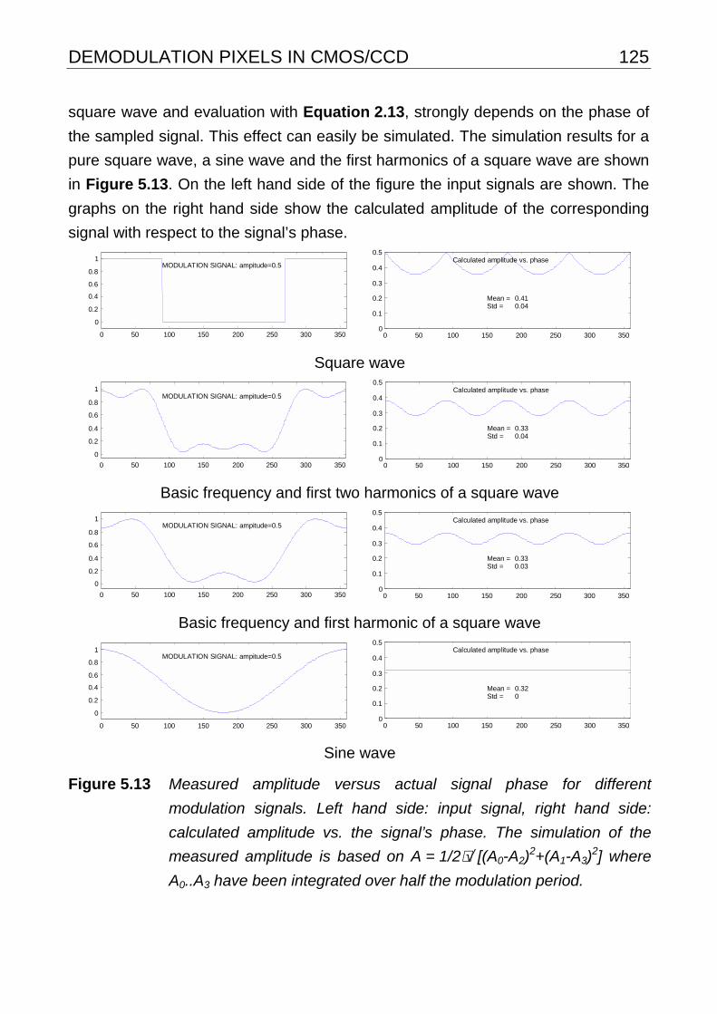
DEMODULATION PIXELS IN CMOS/CCD 125
square wave and evaluation with Equation 2.13, strongly depends on the phase of
the sampled signal. This effect can easily be simulated. The simulation results for a
pure square wave, a sine wave and the first harmonics of a square wave are shown
in Figure 5.13. On the left hand side of the figure the input signals are shown. The
graphs on the right hand side show the calculated amplitude of the corresponding
signal with respect to the signal’s phase.
0 50 100 150 200 250 300 3500
0.1
0.2
0.3
0.4
0.5
Mean = 0.41Std = 0.04
Calculated amplitude vs. phase
0
0.2
0.4
0.6
0.8
1MODULATION SIGNAL: ampitude=0.5
0 50 100 150 200 250 300 350
Square wave
0 50 100 150 200 250 300 3500
0.1
0.2
0.3
0.4
0.5
Mean = 0.33Std = 0.04
Calculated amplitude vs. phase
0
0.2
0.4
0.6
0.8
1MODULATION SIGNAL: ampitude=0.5
0 50 100 150 200 250 300 350
Basic frequency and first two harmonics of a square wave
0 50 100 150 200 250 300 3500
0.1
0.2
0.3
0.4
0.5
Mean = 0.33Std = 0.03
Calculated amplitude vs. phase
0
0.2
0.4
0.6
0.8
1MODULATION SIGNAL: ampitude=0.5
0 50 100 150 200 250 300 350
Basic frequency and first harmonic of a square wave
0 50 100 150 200 250 300 3500
0.1
0.2
0.3
0.4
0.5
Mean = 0.32Std = 0
Calculated amplitude vs. phase
0
0.2
0.4
0.6
0.8
1MODULATION SIGNAL: ampitude=0.5
0 50 100 150 200 250 300 350
Sine wave
Figure 5.13 Measured amplitude versus actual signal phase for different
modulation signals. Left hand side: input signal, right hand side:
calculated amplitude vs. the signal’s phase. The simulation of the
measured amplitude is based on A = 1/2⋅√ [(A0-A2)2+(A1-A3)
2] where
A0..A3 have been integrated over half the modulation period.
126 CHAPTER 5
As one would expect, for the sine wave the measured amplitude does not depend
on the actual phase (no aliasing). The calculated amplitude has a constant value of
0.32, 64% of the real amplitude 0.5. For the square wave, however, the measured
amplitude indeed depends on the actual phase. It varies with a standard deviation
of 0.04, which is a relative amplitude error of ± 8%. Therefore, if we measure the
amplitude of the square wave input signal in order to determine the demodulation
contrast of the pixels, we have to take into account the actual phase between the
optical input signal and the sampling signal of the demodulation pixel.
Now, what does that mean for our measurements? If we look at the optical input
signals, we see that the light source has a low-pass characteristic. For frequencies
higher than about 5 MHz, the optical signal gradually looks like a sine wave
(concerns the 630 nm LEDs that are also used for the range camera realizations).
The delay between the optical modulation signal of the LEDs and the control
voltages for the photogates (signal demodulation) is about 6 ns (measured). This
corresponds to the following phases at the different modulation frequencies:
1 kHz 6 ns = 0.00216°
10 kHz 6 ns = 0.0216°
100 kHz 6 ns = 0.216°
1 MHz 6 ns = 2.16°
10 MHz 6 ns = 21.6°
20 MHz 6 ns = 43.2°
We see that for frequencies less than 10 MHz the delay of 6 ns does not have a
significant influence on the phase. One can see from Figure 5.13 that, as long as
the phase is 0° or any multiple of π/2, the calculated amplitude of a 4-tap sampled
square wave is correct. Therefore, we can use the algorithm
A = 1/2⋅√ [(A0-A2)2+(A1-A3)
2] to calculate the amplitude and hence the demodulation
contrast without taking into account the actual signal phase. For frequencies lower
than 10 MHz the phase of the optical input signals is about 0°, so we do not make
any error in calculating the amplitude of the square wave. For 10 MHz and 20 MHz,
the input signal is nearly a sinusoidal wave, where the measured amplitude does
not depend on the phase. We measure the amplitude with a systematic error of
64% in that case. Strictly speaking, for an isolated determination of the pixels’
demodulation performance at high frequencies one would have to correct the
measured amplitude by a factor of 1 / 0.64 = 1.56. This is because, due to a
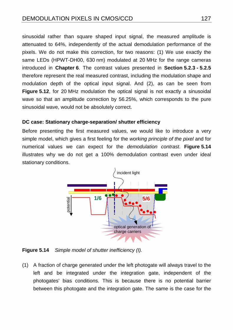
DEMODULATION PIXELS IN CMOS/CCD 127
sinusoidal rather than square shaped input signal, the measured amplitude is
attenuated to 64%, independently of the actual demodulation performance of the
pixels. We do not make this correction, for two reasons: (1) We use exactly the
same LEDs (HPWT-DH00, 630 nm) modulated at 20 MHz for the range cameras
introduced in Chapter 6. The contrast values presented in Section 5.2.3 - 5.2.5
therefore represent the real measured contrast, including the modulation shape and
modulation depth of the optical input signal. And (2), as can be seen from
Figure 5.12, for 20 MHz modulation the optical signal is not exactly a sinusoidal
wave so that an amplitude correction by 56.25%, which corresponds to the pure
sinusoidal wave, would not be absolutely correct.
DC case: Stationary charge-separation/ shutter efficiency
Before presenting the first measured values, we would like to introduce a very
simple model, which gives a first feeling for the working principle of the pixel and for
numerical values we can expect for the demodulation contrast. Figure 5.14
illustrates why we do not get a 100% demodulation contrast even under ideal
stationary conditions.
incident light
optical generation of charge carriers
pot
entia
l 1/6 5/6
Figure 5.14 Simple model of shutter inefficiency (I).
(1) A fraction of charge generated under the left photogate will always travel to the
left and be integrated under the integration gate, independent of the
photogates’ bias conditions. This is because there is no potential barrier
between this photogate and the integration gate. The same is the case for the
128 CHAPTER 5
right photogate, where a fraction of charge will always travel directly into the
dump diffusion and will never be detected.
(2) Charge carriers are not only collected under the transparent photogates but
also under the adjacent opaque photogates, because (a) the geometry and
position of the optical shield is never 100% precise. And (b), even more
important, depending on its wavelength the light penetrates deep into the
semiconductor before it generates electron hole pairs (c.f. Figure 3.4). Then it
diffuses in all directions, not only perpendicularly to the semiconductor surface.
This leads to the blurring effect, which we have already mentioned above.
Here ideal perpendicular diffusion has been assumed. Nevertheless 50% of the
charge generated under the left photo gate cannot be separated and will be
collected under the integration gate. Such a behavior would correspond to a
demodulation contrast of (5/6-1/6) / (5/6+1/6) = 4/6 = 67%.
This means that, for this simple model, we cannot expect the demodulation contrast
to be better than 67%, even for these idealized DC-conditions. So far, however, we
have neglected two important parameters: (1) the demodulation frequency (the
demodulation contrast will decrease with increasing frequencies) and (2) the
influence of the light’s wavelength.
Influence of the wavelength
As already mentioned, we expect the wavelength of the light source used to have
an influence on the achievable demodulation contrast. This is due to the
wavelength-dependent penetration depth of incoming light, introduced in
Section 3.1.1. Since, generally, electrical fields within a CMOS-processed
semiconductor exist only near the semiconductor surface, substrate-regions more
than about 2 µm - 5 µm away from the surface are nearly field-free. Charge carriers
that are optically generated in these regions move by thermal diffusion in any
random direction. Either they recombine within the substrate or they are collected
by an electrical field near the surface. However, they can travel up to 100 µm
before being captured by an electrical field (Section 3.1.3). Since red-light
photoelectrons are generated deeper in the semiconductor than blue-light
photoelectrons, their tendency to travel before being detected (crosstalk) is much
higher.
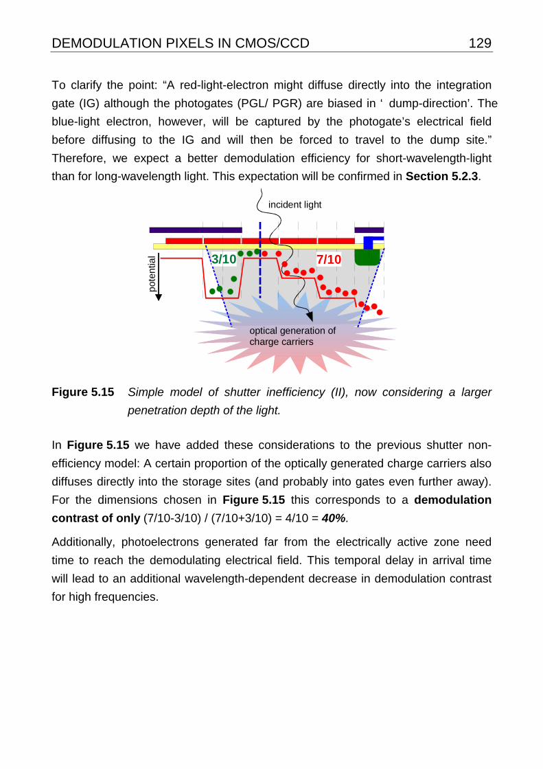
DEMODULATION PIXELS IN CMOS/CCD 129
To clarify the point: “A red-light-electron might diffuse directly into the integration
gate (IG) although the photogates (PGL/ PGR) are biased in ‘dump-direction’. The
blue-light electron, however, will be captured by the photogate’s electrical field
before diffusing to the IG and will then be forced to travel to the dump site.”
Therefore, we expect a better demodulation efficiency for short-wavelength-light
than for long-wavelength light. This expectation will be confirmed in Section 5.2.3.
incident light
optical generation of charge carriers
pot
entia
l 3/10 7/10
Figure 5.15 Simple model of shutter inefficiency (II), now considering a larger
penetration depth of the light.
In Figure 5.15 we have added these considerations to the previous shutter non-
efficiency model: A certain proportion of the optically generated charge carriers also
diffuses directly into the storage sites (and probably into gates even further away).
For the dimensions chosen in Figure 5.15 this corresponds to a demodulation
contrast of only (7/10-3/10) / (7/10+3/10) = 4/10 = 40%.
Additionally, photoelectrons generated far from the electrically active zone need
time to reach the demodulating electrical field. This temporal delay in arrival time
will lead to an additional wavelength-dependent decrease in demodulation contrast
for high frequencies.
130 CHAPTER 5
5.2.3 Determination of optimal control voltages
It is obvious that the demodulation contrast depends on the amplitude of the control
voltages of the photogates. With our control and driving electronics we can switch
the control signals between 0 V and an adjustable voltage value. Additionally, the
setup allows the rise and fall times to be varied by changing an additional
capacitive load on the driver’s output. Also, the pulse width can be varied by some
nanoseconds. The rise and fall times as well as the duty cycle (pulse width) gain
importance only for high modulation frequencies. Since, however, the exact
adjustments of both rise and fall time and signal pulse width are very time-
consuming, we determine the best voltages firstly for 1 MHz and, based on these
results, we only perform a fine-tuning for 20 MHz modulation. For both realizations,
the demodulation contrast reaches a maximum for PGL/PGR modulated with 8 V
amplitude (Figure 5.16). The ideal voltage of the middle photogate at 20 MHz
modulation frequency is 3.5 V for the BCCD version and 6.5 V for the SCCD.
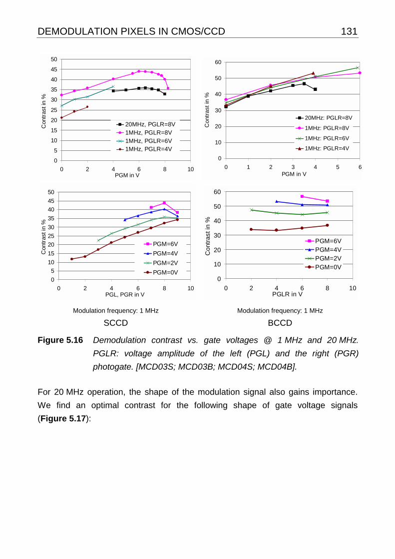
DEMODULATION PIXELS IN CMOS/CCD 131
0
5
10
15
20
25
30
35
40
45
50
0 2 4 6 8 10PGM in V
Con
tras
t in
%
20MHz, PGLR=8V1MHz, PGLR=8V1MHz, PGLR=6V1MHz, PGLR=4V
0
10
20
30
40
50
60
0 1 2 3 4 5 6PGM in V
Contr
ast
in %
20MHz: PGLR=8V
1MHz: PGLR=8V
1MHz: PGLR=6V
1MHz: PGLR=4V
0
5
10
15
20
25
30
35
40
45
50
0 2 4 6 8 10PGL, PGR in V
Con
tras
t in
%
PGM=6V
PGM=4V
PGM=2V
PGM=0V
Modulation frequency: 1 MHz
0
10
20
30
40
50
60
0 2 4 6 8 10PGLR in V
Co
ntra
st in
%
PGM=6VPGM=4VPGM=2VPGM=0V
Modulation frequency: 1 MHz
SCCD BCCD
Figure 5.16 Demodulation contrast vs. gate voltages @ 1 MHz and 20 MHz.
PGLR: voltage amplitude of the left (PGL) and the right (PGR)
photogate. [MCD03S; MCD03B; MCD04S; MCD04B].
For 20 MHz operation, the shape of the modulation signal also gains importance.
We find an optimal contrast for the following shape of gate voltage signals
(Figure 5.17):
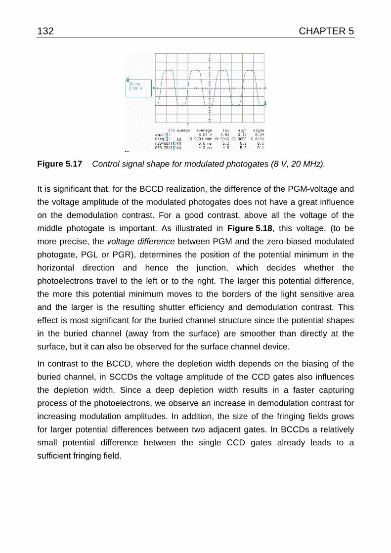
132 CHAPTER 5
Figure 5.17 Control signal shape for modulated photogates (8 V, 20 MHz).
It is significant that, for the BCCD realization, the difference of the PGM-voltage and
the voltage amplitude of the modulated photogates does not have a great influence
on the demodulation contrast. For a good contrast, above all the voltage of the
middle photogate is important. As illustrated in Figure 5.18, this voltage, (to be
more precise, the voltage difference between PGM and the zero-biased modulated
photogate, PGL or PGR), determines the position of the potential minimum in the
horizontal direction and hence the junction, which decides whether the
photoelectrons travel to the left or to the right. The larger this potential difference,
the more this potential minimum moves to the borders of the light sensitive area
and the larger is the resulting shutter efficiency and demodulation contrast. This
effect is most significant for the buried channel structure since the potential shapes
in the buried channel (away from the surface) are smoother than directly at the
surface, but it can also be observed for the surface channel device.
In contrast to the BCCD, where the depletion width depends on the biasing of the
buried channel, in SCCDs the voltage amplitude of the CCD gates also influences
the depletion width. Since a deep depletion width results in a faster capturing
process of the photoelectrons, we observe an increase in demodulation contrast for
increasing modulation amplitudes. In addition, the size of the fringing fields grows
for larger potential differences between two adjacent gates. In BCCDs a relatively
small potential difference between the single CCD gates already leads to a
sufficient fringing field.
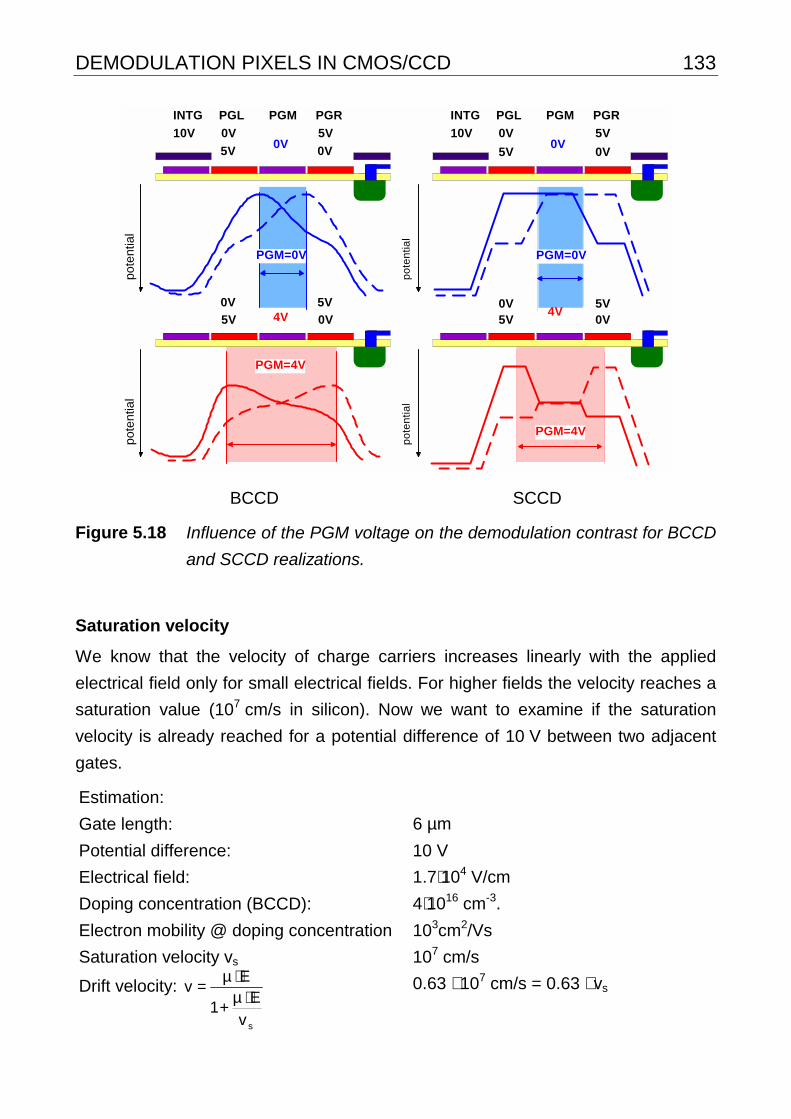
DEMODULATION PIXELS IN CMOS/CCD 133
po
ten
tial
10V 0V0V
5V
INTG PGL PGM PGR
5V 4V 0V
po
ten
tial
PGM=4V
po
ten
tial
10V 0V0V
5V
INTG PGL PGM PGR
5V4V
0V
po
ten
tial
PGM=4V
5V 0V
0V 5V 0V 5V
5V 0V
PGM=0V PGM=0V
BCCD SCCD
Figure 5.18 Influence of the PGM voltage on the demodulation contrast for BCCD
and SCCD realizations.
Saturation velocity
We know that the velocity of charge carriers increases linearly with the applied
electrical field only for small electrical fields. For higher fields the velocity reaches a
saturation value (107 cm/s in silicon). Now we want to examine if the saturation
velocity is already reached for a potential difference of 10 V between two adjacent
gates.
Estimation:
Gate length: 6 µm
Potential difference: 10 V
Electrical field: 1.7⋅104 V/cm
Doping concentration (BCCD): 4⋅1016 cm-3.
Electron mobility @ doping concentration 103cm2/Vs
Saturation velocity vs 107 cm/s
Drift velocity:
sv
E1
Ev
⋅µ+
⋅µ= 0.63 ⋅ 107 cm/s = 0.63 ⋅ vs
134 CHAPTER 5
We see that even for 10 V the saturation velocity is not yet reached. The results we
presented (increase in demodulation contrast for increased PGL / PGR voltage) are
reasonable because an increase in electrical field still causes an increased drift
velocity and hence faster response of charge carriers to the electrical field, leading
to a better demodulation contrast at high modulation frequencies.
5.2.4 Influence of optical power and integration time @ 20MHz
We discussed in Section 3.2 that the charge transfer efficiency of CCDs strongly
depends on the number of charge carriers that are contained in the charge packet
to transport (c.f. Figure 3.20). Therefore we expect the optical power, i.e. how
many photoelectrons are generated (and hence have to be transported) per unit
time, to have a noticeable influence on the demodulation contrast. This is
investigated in the current section.
In order to measure the influence of the number of generated photoelectrons per
unit time on the contrast, two parameters are changed: (1) the optical power and (2)
the integration times. For a good reproducibility of the measurements we keep the
output power of the LED constant and use neutral density filters (ND) to attenuate
the power on the pixel. This has the advantage that the LED can be operated with
the same mean current (50 mA) for all measurements. (Because of a current-
dependent operating temperature, the LED changes its dynamic characteristics for
different control currents). For each integration time we chose a different spot size
(by adjusting the distance of the microscope’s objective to the sensor chip), the
exact parameters are summarized in MCD05 in the appendix.
We carry out measurements of the demodulation contrast for 4 different optical
power conditions (1) without ND filter, (2) with 27% ND filter (3) with 8% ND filter
and (4) with both intensity filters (2% attenuation). Since the total optical power and
the size of the light spot are measured, we can recalculate the optical power on the
light sensitive area of each pixel. The dark current is measured separately and
subtracted from the measured values before calculating the demodulation contrast.
These measurements have only been performed for the surface-channel realization
(SCCD); the results are shown in Figure 5.19 and Figure 5.20.
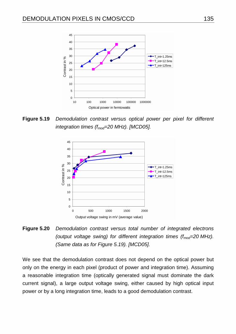
DEMODULATION PIXELS IN CMOS/CCD 135
0
5
10
15
20
25
30
35
40
45
10 100 1000 10000 100000 1000000
Optical power in femtowatts
Co
ntr
ast
in %
T_int=1.25ms
T_int=12.5ms
T_int=125ms
Figure 5.19
Demodulation contrast versus optical power per pixel for different
integration times (fmod=20 MHz). [MCD05].
0
5
10
15
20
25
30
35
40
45
0 500 1000 1500 2000
Output voltage swing in mV (average value)
Co
ntr
ast
in % T_int=1.25ms
T_int=12.5ms
T_int=125ms
Figure 5.20
Demodulation contrast versus total number of integrated electrons
(output voltage swing) for different integration times (fmod=20 MHz).
(Same data as for Figure 5.19). [MCD05].
We see that the demodulation contrast does not depend on the optical power but
only on the energy in each pixel (product of power and integration time). Assuming
a reasonable integration time (optically generated signal must dominate the dark
current signal), a large output voltage swing, either caused by high optical input
power or by a long integration time, leads to a good demodulation contrast.
136 CHAPTER 5
This is only possible, since the CCD-performance of adding and storing signals in
the charge domain is nearly noise-free. Normally, one would expect a lower optical
power to lead to a worse demodulation contrast, since we know, from CTE
measurements of CCDs that are realized in the same technology, that the CTE is
better, the more charge is to be transported (c.f. Figure 3.20). This is because all
three transport mechanisms (self-induced drift, diffusion and fringing fields)
contribute to the charge transport. Self-induced drift strongly depends on the
number of integrated electrons, because a smaller number of electrons leads to a
reduced influence of self-induced drift on the overall charge transfer.
For 20 MHz modulation, the short-time integration lasts only 25 ns (50 ns
modulation period). In this period, only few electrons are generated and transported
to the integration gate. In fact, as one can see from MCD05, for 175,000
femtowatts, the highest optical power used, only 18 electrons are generated within
50ns, statistically speaking, i.e. only 9 electrons within the active sampling time. For
the lowest optical power used the conditions are much worse: one electron is
generated, statistically speaking, only every 300th modulation period. From these
numbers, we understand that, under the above conditions, self-induced drift can
have no influence at all on the charge transfer. We really move single electrons.
Demodulation only works here with the help of statistics. This enormous
performance is a big welcome surprise.
In addition to the total optical power on one photogate, the average resulting output
voltage swing is also listed in MCD05. This can be calculated with known quantum
efficiency, wavelength, integration time, conversion capacitance and amplification
of the output stage. Also the total number of electrons generated during the
integration time is listed, as well as the number of electrons statistically generated
during only one modulation period. Since these values are smaller than one, it is
more meaningful to list the inverse value, which is the number of modulation cycles
that have to pass until one electron is optically generated by the modulated light
source, statistically speaking.

DEMODULATION PIXELS IN CMOS/CCD 137
5.2.5 Demodulation contrast versus frequency and wavelength
The application areas of the TOF- range cameras are essentially restricted by two
important parameters: the required range resolution and the wavelength of the light
used. While almost all range measurement applications demand the best possible
range resolution, which requires a good demodulation bandwidth of the pixels,
some applications additionally require the use of near infrared light (invisible for the
human eye).
In this section we present the measurements of demodulation contrast for different
modulation frequencies and wavelengths of the light source. As light sources, we
use different kinds of LEDs. They all have a characteristic response time and
dynamic behavior. We operate them with the MICROCHOP module MV-LED1
[CS1], a fast LED driver module for the microbench. Figure 5.21 shows the
measured modulated output signal of all the LEDs that we use.
470 nm-LED signal @ 20 MHz
(20 ns/div) 740 nm-LED signal @ 20 MHz
(20 ns/div) 850 nm-LED signal @ 200 kHz
(1 µs/div)
630 nm-LED signal @ 20 MHz
(20 ns/div) 850 nm-LED signal @ 1 MHz
(0.5 µs/div)
Figure 5.21 Signal shape of the used LEDs for different modulation frequencies.
(Measured with FEMTO 500 MHz photodiode module [FEM]
PR-X-500M-SI-DC).
The 850 nm LED can obviously only be used up to 1 MHz, since its characteristic
20% / 80%-rise time of about 500 ns does not allow faster modulation. The output
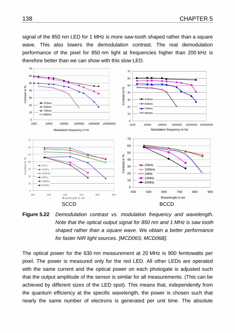
138 CHAPTER 5
signal of the 850 nm LED for 1 MHz is more saw-tooth shaped rather than a square
wave. This also lowers the demodulation contrast. The real demodulation
performance of the pixel for 850 nm light at frequencies higher than 200 kHz is
therefore better than we can show with this slow LED.
0
10
20
30
40
50
60
70
1000 10000 100000 1000000 10000000 100000000
Modulation frequency in Hz
Con
tras
t in
%
470nm
630nm
740nm
850nm
0
10
20
30
40
50
60
70
1000 10000 100000 1000000 10000000 100000000
Modulation frequency in Hz
Co
ntra
st in
%
470nm
630nm
740nm
850nm
0
10
20
30
40
50
60
70
400 500 600 700 800 900W a ve le n g th in n m
Co
ntr
ast
in %
1k H z
10kH z
100k H z
1MH z
10MH z
20MH z
0
10
20
30
40
50
60
70
400 500 600 700 800 900
Wavelength in nm
Co
ntr
ast
in %
10kHz
100kHz1MHz
10MHz20MHz
SCCD BCCD
Figure 5.22 Demodulation contrast vs. modulation frequency and wavelength.
Note that the optical output signal for 850 nm and 1 MHz is saw tooth
shaped rather than a square wave. We obtain a better performance
for faster NIR light sources. [MCD06S; MCD06B].
The optical power for the 630 nm measurement at 20 MHz is 900 femtowatts per
pixel. The power is measured only for the red LED. All other LEDs are operated
with the same current and the optical power on each photogate is adjusted such
that the output amplitude of the sensor is similar for all measurements. (This can be
achieved by different sizes of the LED spot). This means that, independently from
the quantum efficiency at the specific wavelength, the power is chosen such that
nearly the same number of electrons is generated per unit time. The absolute
DEMODULATION PIXELS IN CMOS/CCD 139
optical power, used for the other wavelengths (470 nm, 740 nm, and 850 nm), can
be recalculated from the ratio of the measured mean values of the sampling and
the quantum efficiency of the specific wavelength, which is known. The
measurement results are summarized in Figure 5.22. With another infrared LED,
emitting at 810 nm (manufacturer: EPIGAP), we obtain a demodulation contrast of
better than 25% at 20 MHz.
The measurements show the expected contrast decrease for high frequencies and
longer wavelengths (c.f. Section 5.2.2). Especially for high frequencies, the BCCD
performance is superior to that of the SCCD. For 20 MHz modulation and 630 nm
wavelength we still achieve a modulation contrast of better than 40% with the
BCCD version, which is still quite good compared to the DC performance of about
60%. Furthermore, we can state that the simple model described in Figure 5.14
and Figure 5.15 makes an astonishingly good performance prediction for the DC
case.
5.2.6 Phase accuracy measurements
In the previous sections, we presented measurements of the 1-tap pixel’s
demodulation contrast versus several parameters for the BCCD and the SCCD
realization of the 1-tap pixel. In the following we will only consider the BCCD
version. In fact, however, we are interested in the time or phase resolution offered
by the demodulation pixels. For a real distance measurement, the received optical
power varies with the distance of the target. It is therefore not practical to
characterize the time resolution with a distance measurement setup, because at the
same time the time delay (distance) changes; also the received power would
change. With such a setup one cannot measure the time resolution isolated from
the received power.
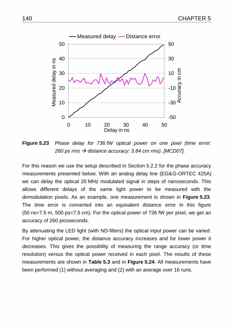
140 CHAPTER 5
0
10
20
30
40
50
0 10 20 30 40 50Delay in ns
Mea
sure
d de
lay
in n
s
-50
-30
-10
10
30
50
Acc
urac
y in
cm
Measured delay Distance error
Figure 5.23 Phase delay for 736 fW optical power on one pixel (time error:
260 ps rms ! distance accuracy: 3.84 cm rms). [MCD07].
For this reason we use the setup described in Section 5.2.2 for the phase accuracy
measurements presented below. With an analog delay line (EG&G-ORTEC 425A)
we can delay the optical 20 MHz modulated signal in steps of nanoseconds. This
allows different delays of the same light power to be measured with the
demodulation pixels. As an example, one measurement is shown in Figure 5.23.
The time error is converted into an equivalent distance error in this figure
(50 ns=7.5 m, 500 ps=7.5 cm). For the optical power of 736 fW per pixel, we get an
accuracy of 260 picoseconds.
By attenuating the LED light (with ND-filters) the optical input power can be varied.
For higher optical power, the distance accuracy increases and for lower power it
decreases. This gives the possibility of measuring the range accuracy (or time
resolution) versus the optical power received in each pixel. The results of these
measurements are shown in Table 5.3 and in Figure 5.24. All measurements have
been performed (1) without averaging and (2) with an average over 16 runs.
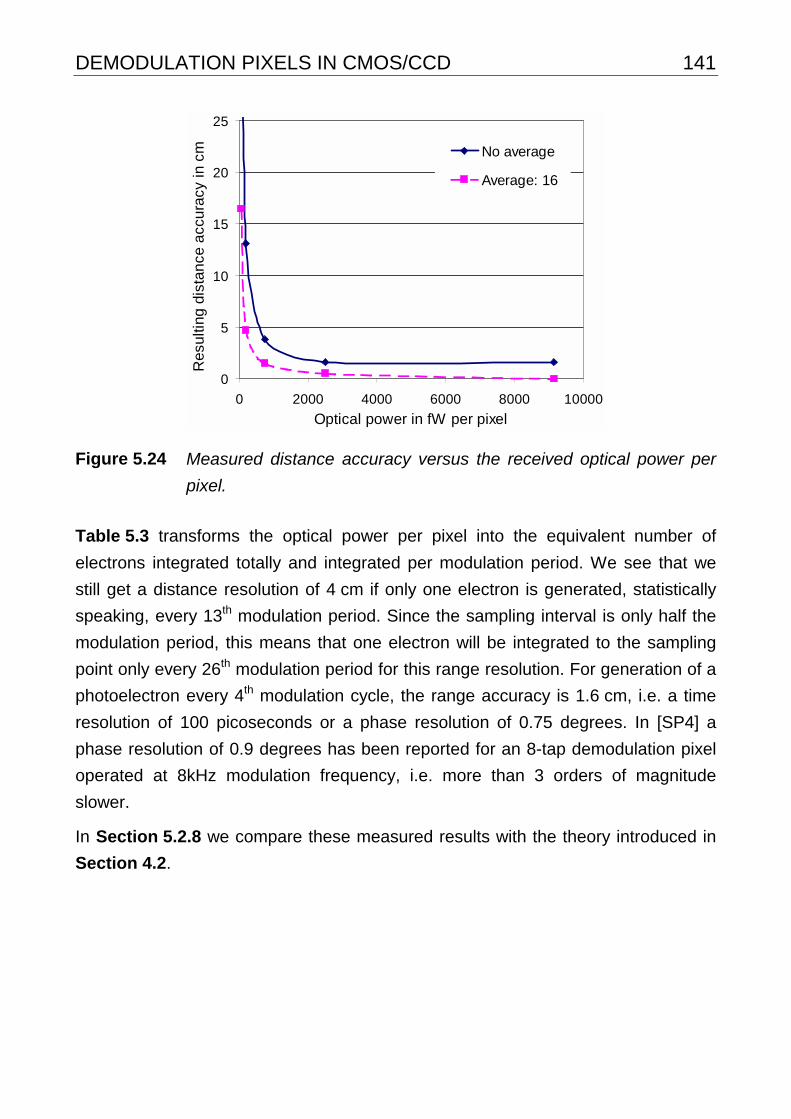
DEMODULATION PIXELS IN CMOS/CCD 141
0
5
10
15
20
25
0 2000 4000 6000 8000 10000
Optical power in fW per pixel
Res
ulti
ng
dis
tan
ce a
ccu
racy
in c
m No average
Average: 16
Figure 5.24 Measured distance accuracy versus the received optical power per
pixel.
Table 5.3 transforms the optical power per pixel into the equivalent number of
electrons integrated totally and integrated per modulation period. We see that we
still get a distance resolution of 4 cm if only one electron is generated, statistically
speaking, every 13th modulation period. Since the sampling interval is only half the
modulation period, this means that one electron will be integrated to the sampling
point only every 26th modulation period for this range resolution. For generation of a
photoelectron every 4th modulation cycle, the range accuracy is 1.6 cm, i.e. a time
resolution of 100 picoseconds or a phase resolution of 0.75 degrees. In [SP4] a
phase resolution of 0.9 degrees has been reported for an 8-tap demodulation pixel
operated at 8kHz modulation frequency, i.e. more than 3 orders of magnitude
slower.
In Section 5.2.8 we compare these measured results with the theory introduced in
Section 4.2.
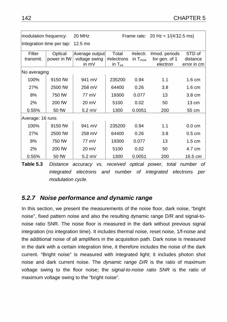
142 CHAPTER 5
modulation frequency: 20 MHz
Integration time per tap: 12.5 ms
Frame rate: 20 Hz = 1/(4⋅12.5 ms)
Filter transmit.
Optical power in fW
Average output voltage swing
in mV
Total #electrons
in Tint
#electr. in Tmod
#mod. periods for gen. of 1
electron
STD of distance
error in cm
No averaging
100% 9150 fW 941 mV 235200 0.94 1.1 1.6 cm
27% 2500 fW 258 mV 64400 0.26 3.8 1.6 cm
8% 750 fW 77 mV 19300 0.077 13 3.8 cm
2% 200 fW 20 mV 5100 0.02 50 13 cm
0.55% 50 fW 5.2 mV 1300 0.0051 200 55 cm
Average: 16 runs
100% 9150 fW 941 mV 235200 0.94 1.1 0.0 cm
27% 2500 fW 258 mV 64400 0.26 3.8 0.5 cm
8% 750 fW 77 mV 19300 0.077 13 1.5 cm
2% 200 fW 20 mV 5100 0.02 50 4.7 cm
0.55% 50 fW 5.2 mV 1300 0.0051 200 16.5 cm
Table 5.3 Distance accuracy vs. received optical power, total number of
integrated electrons and number of integrated electrons per
modulation cycle.
5.2.7 Noise performance and dynamic range
In this section, we present the measurements of the noise floor, dark noise, “bright
noise”, fixed pattern noise and also the resulting dynamic range D/R and signal-to-
noise ratio SNR. The noise floor is measured in the dark without previous signal
integration (no integration time). It includes thermal noise, reset noise, 1/f-noise and
the additional noise of all amplifiers in the acquisition path. Dark noise is measured
in the dark with a certain integration time, it therefore includes the noise of the dark
current. “Bright noise” is measured with integrated light; it includes photon shot
noise and dark current noise. The dynamic range D/R is the ratio of maximum
voltage swing to the floor noise; the signal-to-noise ratio SNR is the ratio of
maximum voltage swing to the “bright noise”.
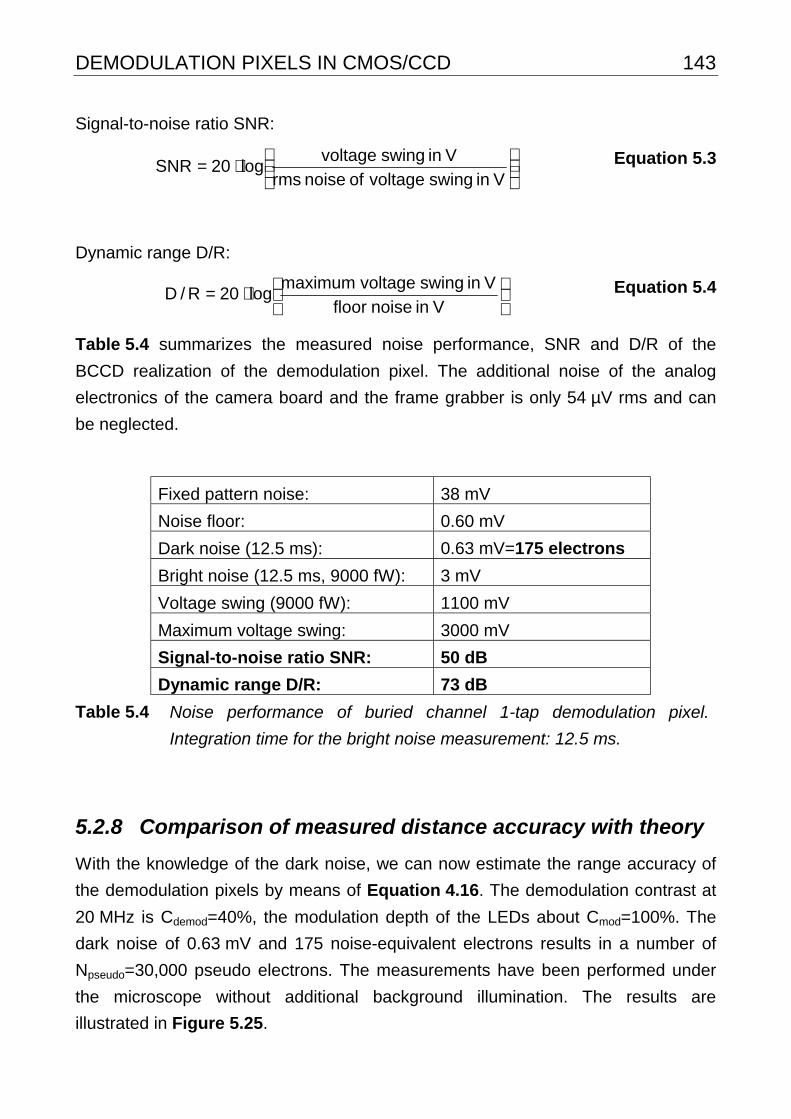
DEMODULATION PIXELS IN CMOS/CCD 143
Signal-to-noise ratio SNR:
⋅=
Vin swing voltage of noise rms
Vin swing voltagelog20SNR Equation 5.3
Dynamic range D/R:
⋅=
Vin noise floor
Vin swing voltage maximumlog20R/D Equation 5.4
Table 5.4 summarizes the measured noise performance, SNR and D/R of the
BCCD realization of the demodulation pixel. The additional noise of the analog
electronics of the camera board and the frame grabber is only 54 µV rms and can
be neglected.
Fixed pattern noise: 38 mV
Noise floor: 0.60 mV
Dark noise (12.5 ms): 0.63 mV=175 electrons
Bright noise (12.5 ms, 9000 fW): 3 mV
Voltage swing (9000 fW): 1100 mV
Maximum voltage swing: 3000 mV
Signal-to-noise ratio SNR: 50 dB
Dynamic range D/R: 73 dB
Table 5.4 Noise performance of buried channel 1-tap demodulation pixel.
Integration time for the bright noise measurement: 12.5 ms.
5.2.8 Comparison of measured distance accuracy with theory
With the knowledge of the dark noise, we can now estimate the range accuracy of
the demodulation pixels by means of Equation 4.16. The demodulation contrast at
20 MHz is Cdemod=40%, the modulation depth of the LEDs about Cmod=100%. The
dark noise of 0.63 mV and 175 noise-equivalent electrons results in a number of
Npseudo=30,000 pseudo electrons. The measurements have been performed under
the microscope without additional background illumination. The results are
illustrated in Figure 5.25.

144 CHAPTER 5
#Pseudo background electrons (floor noise): 30’000
Modulation depth of the LEDs Cmod: 1
Demodulation contrast Cdemod: 0.4
“L” (Non-ambiguity distance range):
750cm
Optical mean power in fW: 9150 2500 750 200 50
Resulting #photoelectrons PEopt: 235000 64000 19000 5100 1300
Sigma in cm (theory): 0.7 1.6 3.9 12.2 45.1
Sigma in cm (measured): 1.6 1.6 3.8 13.1 55.3
These results are also plotted in the following graph and referenced in
Section 5.2.6.
0
5
10
15
20
0 2500 5000 7500 10000
Optical power in fW per pixel
Res
olu
tion
in c
m
Measurement
Theory
Figure 5.25 Estimated and measured distance resolution versus received optical
power per pixel. (Integration time: 12.5 ms per sampling point,
total 50 ms.)
This excellent fit between measurement and theory confirms the validity of
Equation 4.16, which gives us the possibility to predict the range accuracy for
given measurement conditions.
DEMODULATION PIXELS IN CMOS/CCD 145
5.2.9 Summary
The demodulation contrast depends on several parameters: amplitude of gate
voltages, demodulation frequency, received optical power density and wavelength
of modulated light. Since the CCD shutter mechanism used never has 100%
efficiency, even under DC conditions, the demodulation contrast is never better
than about 60%.
The contrast decreases with higher modulation frequencies, since the
photoelectrons do not have enough time to reach the storage site (dump site
respectively). The gate voltages PGL and PGR should be chosen to be as high as
possible. This is in order to generate high electrical fields in the semiconductor.
Even for a voltage difference of 10 V between two adjacent photogates, the
saturation velocity of electrons is not yet reached. Therefore, the experimentally
measured optimum gate voltages of about 8 V are reasonable: an increase in
electrical field still causes an increased drift velocity and hence faster response of
charge carriers to the electrical field. For modulation voltages higher than 8 V the
maximum signal that can be handled decreases, since the charge handling
capability of the pixel is essentially influenced by the potential difference between
the modulation gate PGL and the integration gate IG (10.7 V).
Furthermore, the demodulation contrast decreases with increasing wavelength.
This is because the light penetrates deeper into the semiconductor before
photoelectrons are generated. These photoelectrons then need more time to reach
the depletion region, where they are separated to the dump- or integration site,
depending on their arrival. Also photoelectrons generated far from the surface
diffuse in random directions, so that they are equally likely to travel directly to the
integration or dump site, independently of the actual biasing conditions of the
modulated photogates PGL and PGR.
For the BCCD realization of the 1-tap demodulation pixel we have measured a
contrast of 40% using 20 MHz (more or less) sinusoidally modulated light of 630 nm
wavelength. The SCCD performance is only slightly worse, so that the availability of
a buried channel process option is not necessarily needed. For lower modulation
frequencies and blue light the contrast is better than 60%, quite close to the
prediction of the simple model introduced in Figure 5.14. The contrast decrease
towards higher modulation frequencies can at least partly be attributed to the more

146 CHAPTER 5
sinusoidal rather than square shaped modulation signal. This also explains the less
significant contrast decrease for the faster blue LED at high modulation frequencies
(c.f. Figure 5.21 and Figure 5.22).
With our measurements we could prove the validity of the theoretical range
accuracy predictions presented in Chapter 4. The actual surprise of the
measurements is that demodulation still works excellently if single electrons appear
only every 10th (3 cm range resolution) or even 50th (13 cm range resolution)
modulation cycle (50 ns), assuming an integration time of 50 ms. This astonishingly
low optical generation rate of photoelectrons corresponds to a photocurrent of only
320 fA (1 electron in 10⋅50 ns) or even only 64 fA, respectively (1 electron in
50⋅50 ns).
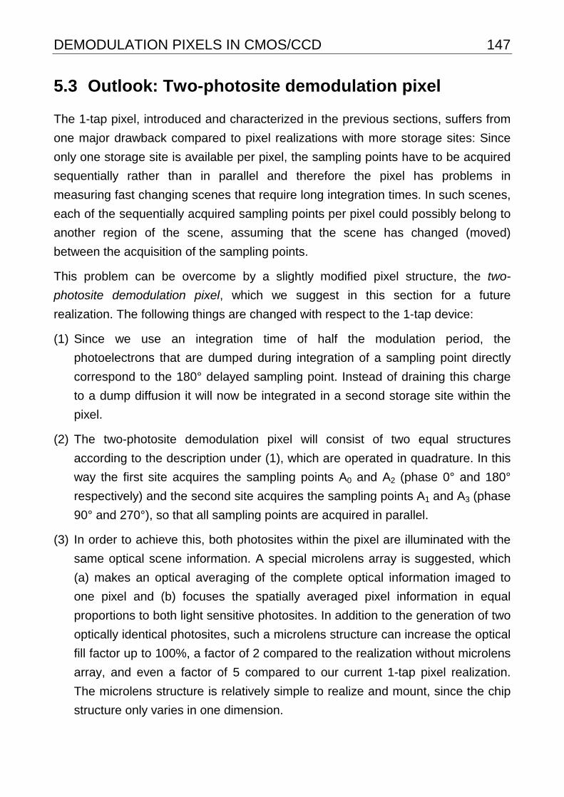
DEMODULATION PIXELS IN CMOS/CCD 147
5.3 Outlook: Two-photosite demodulation pixel
The 1-tap pixel, introduced and characterized in the previous sections, suffers from
one major drawback compared to pixel realizations with more storage sites: Since
only one storage site is available per pixel, the sampling points have to be acquired
sequentially rather than in parallel and therefore the pixel has problems in
measuring fast changing scenes that require long integration times. In such scenes,
each of the sequentially acquired sampling points per pixel could possibly belong to
another region of the scene, assuming that the scene has changed (moved)
between the acquisition of the sampling points.
This problem can be overcome by a slightly modified pixel structure, the two-
photosite demodulation pixel, which we suggest in this section for a future
realization. The following things are changed with respect to the 1-tap device:
(1) Since we use an integration time of half the modulation period, the
photoelectrons that are dumped during integration of a sampling point directly
correspond to the 180° delayed sampling point. Instead of draining this charge
to a dump diffusion it will now be integrated in a second storage site within the
pixel.
(2) The two-photosite demodulation pixel will consist of two equal structures
according to the description under (1), which are operated in quadrature. In this
way the first site acquires the sampling points A0 and A2 (phase 0° and 180°
respectively) and the second site acquires the sampling points A1 and A3 (phase
90° and 270°), so that all sampling points are acquired in parallel.
(3) In order to achieve this, both photosites within the pixel are illuminated with the
same optical scene information. A special microlens array is suggested, which
(a) makes an optical averaging of the complete optical information imaged to
one pixel and (b) focuses the spatially averaged pixel information in equal
proportions to both light sensitive photosites. In addition to the generation of two
optically identical photosites, such a microlens structure can increase the optical
fill factor up to 100%, a factor of 2 compared to the realization without microlens
array, and even a factor of 5 compared to our current 1-tap pixel realization.
The microlens structure is relatively simple to realize and mount, since the chip
structure only varies in one dimension.
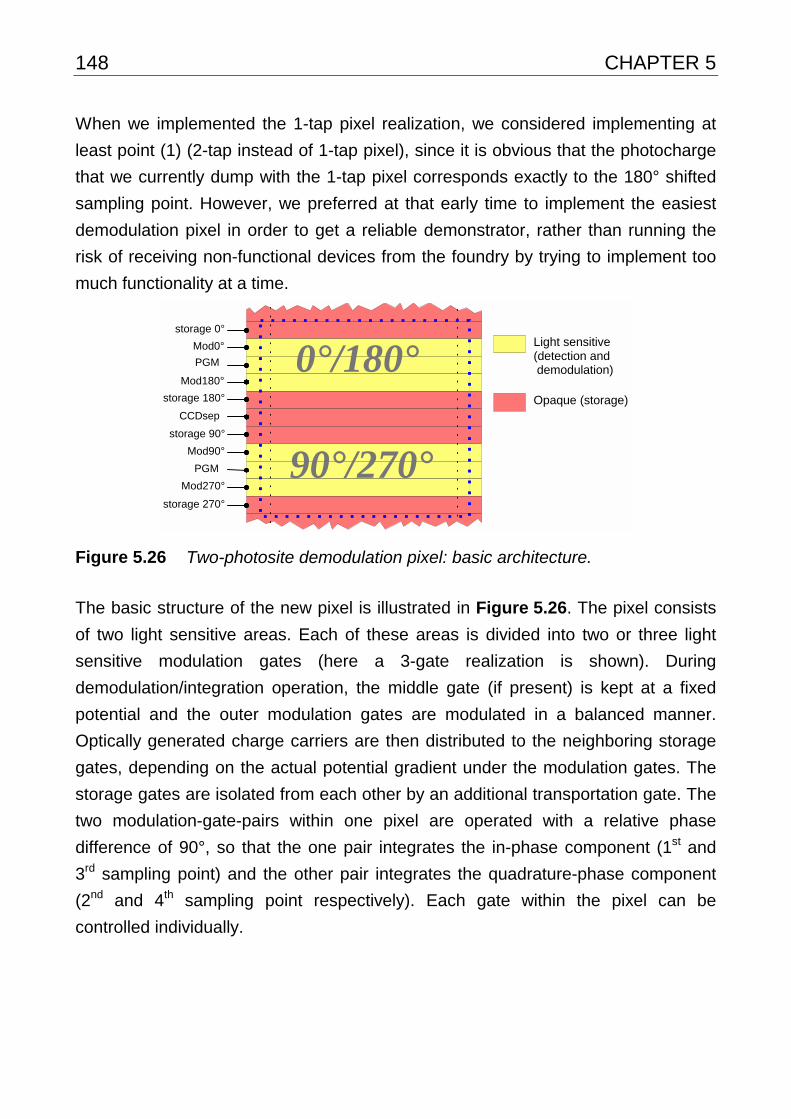
148 CHAPTER 5
When we implemented the 1-tap pixel realization, we considered implementing at
least point (1) (2-tap instead of 1-tap pixel), since it is obvious that the photocharge
that we currently dump with the 1-tap pixel corresponds exactly to the 180° shifted
sampling point. However, we preferred at that early time to implement the easiest
demodulation pixel in order to get a reliable demonstrator, rather than running the
risk of receiving non-functional devices from the foundry by trying to implement too
much functionality at a time.
storage 0°
storage 180°
storage 90°
storage 270°
Mod0°
Mod180°
Mod90°
Mod270°
0°/180°
90°/270°
PGM
PGM
CCDsep
Light sensitive(detection and demodulation)
Opaque (storage)
Figure 5.26 Two-photosite demodulation pixel: basic architecture.
The basic structure of the new pixel is illustrated in Figure 5.26. The pixel consists
of two light sensitive areas. Each of these areas is divided into two or three light
sensitive modulation gates (here a 3-gate realization is shown). During
demodulation/integration operation, the middle gate (if present) is kept at a fixed
potential and the outer modulation gates are modulated in a balanced manner.
Optically generated charge carriers are then distributed to the neighboring storage
gates, depending on the actual potential gradient under the modulation gates. The
storage gates are isolated from each other by an additional transportation gate. The
two modulation-gate-pairs within one pixel are operated with a relative phase
difference of 90°, so that the one pair integrates the in-phase component (1st and
3rd sampling point) and the other pair integrates the quadrature-phase component
(2nd and 4th sampling point respectively). Each gate within the pixel can be
controlled individually.
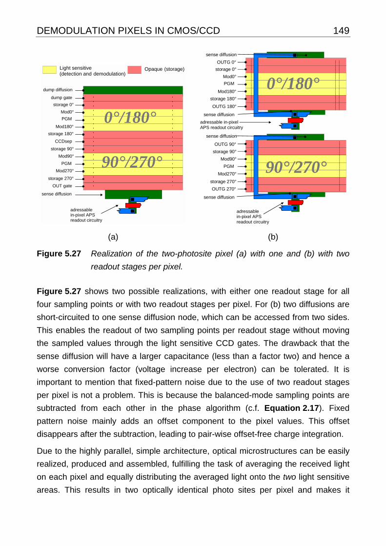
DEMODULATION PIXELS IN CMOS/CCD 149
dump gate
storage 180°
storage 90°
storage 270°
Mod0°
Mod180°
Mod90°
Mod270°
0°/180°
90°/270°
PGM
PGM
CCDsep
adressable in-pixel APSreadout circuitry
storage 0°
dump diffusion
OUT gate
sense diffusion
Light sensitive (detection and demodulation)
Opaque (storage)
(a)
OUTG 0°
storage 180°
storage 90°
storage 270°
Mod0°
Mod180°
Mod90°
Mod270°
0°/180°
90°/270°
PGM
PGM
adressable in-pixel APSreadout circuitry
storage 0°
OUTG 270°
sense diffusion
adressable in-pixelAPS readout circuitry
OUTG 180°
sense diffusion
OUTG 90°
sense diffusion
sense diffusion
(b)
Figure 5.27 Realization of the two-photosite pixel (a) with one and (b) with two
readout stages per pixel.
Figure 5.27 shows two possible realizations, with either one readout stage for all
four sampling points or with two readout stages per pixel. For (b) two diffusions are
short-circuited to one sense diffusion node, which can be accessed from two sides.
This enables the readout of two sampling points per readout stage without moving
the sampled values through the light sensitive CCD gates. The drawback that the
sense diffusion will have a larger capacitance (less than a factor two) and hence a
worse conversion factor (voltage increase per electron) can be tolerated. It is
important to mention that fixed-pattern noise due to the use of two readout stages
per pixel is not a problem. This is because the balanced-mode sampling points are
subtracted from each other in the phase algorithm (c.f. Equation 2.17). Fixed
pattern noise mainly adds an offset component to the pixel values. This offset
disappears after the subtraction, leading to pair-wise offset-free charge integration.
Due to the highly parallel, simple architecture, optical microstructures can be easily
realized, produced and assembled, fulfilling the task of averaging the received light
on each pixel and equally distributing the averaged light onto the two light sensitive
areas. This results in two optically identical photo sites per pixel and makes it
150 CHAPTER 5
insensitive to edges or, generally speaking, to any spatial inhomogeniety imaged on
one pixel. Such an optical structure is sketched in Figure 5.28.
Pixel
focused pixel illumination, distributedin two optically identical areas
standard objective
scene imagedon one pixel
scene
microlensarray
OptoASIC
imagedscene
optical microstructure
Figure 5.28 Microlens structure.
Like the 4-tap lock-in pixel (Section 5.1.2), the two-photosite demodulation pixel
also contains four storage sites. But rather than accessing only one photosite from
four sides, which leads to unsymmetrical sampling point sensitivity due to process
inaccuracies, with this new pixel, two optically identical photosites are accessed
from only two opposite sides. This two-side access is far less sensitive to process
variations than the access from 4 sides. Also the photo site can be easily divided
into several gates to accelerate photoelectrons and to achieve an efficient charge
transfer.
IMAGING TOF RANGE CAMERAS 151
6. Imaging TOF range cameras
Now we introduce the time-of-flight range cameras that we realized with our 1-Tap
lock-in pixel arrays. As mentioned before, we have implemented the demodulation
pixel as a line sensor, carrying 108 pixels and, in a second fabrication run, as a
TOF-imager with 64 by 25 pixels. With these sensors we realized both a 2D TOF
line camera and a 3D TOF imager. Both range cameras are controlled by a fast,
flexible and compact digital sequencer. The sensor chip itself is plugged into a
specially designed driver board, also a very flexible realization that allows the
connection of nine DC levels and 24 AC signals (generated by the sequencer) of
variable amplitude, variable rise and fall time and variable pulse width to any of the
sensor’s pins. The architectural setup of these camera PCBs is roughly described
below. Also we introduce the LEDs that we use for the modulated light source as
well as the corresponding driving electronics.
In the second and third section of this chapter we then present both range camera
realizations, which mainly differ in the LED arrangement of the illumination unit, the
demodulation detector itself and the control-firmware loaded into the sequencer.
Each of these sections starts with an overview of the sensor architecture, then
describes the overall camera system architecture and finally introduces typical
range measurements of non-cooperative scenes that we performed with the
cameras.
152 CHAPTER 6
6.1 Camera electronics
6.1.1 Digital sequencer board
The task of the digital sequence unit is to generate bit patterns that control both the
TOF-sensor chip and the modulated illumination unit. Since no delay lines are
used, the four phase relations between sensor timing and illumination timing (0°,
90°, 180°, 270° and 1st to 4th sampling point respectively), have to be generated
digitally. For our targeted modulation frequency of 20 MHz we therefore need
flexible digital circuitry that can be operated at 80 MHz and beyond.
One possible solution is the realization of a RAM-based sequencer, where a
complete bit-pattern is loaded into a memory, which is then repeatedly read out at
80 MHz frequency (Tbit=12.5 ns). Assuming a 5 Hz frame rate (Tframe=200 ms),
however, a memory size of 2 megabytes per digital channel (200 ms/12.5 ns
=16,000,000 bit) would be necessary, i.e. 48 megabytes for 24 channels
(@ 80 MHz and 200 ms frames). Such a RAM-based sequencer solution is surely
possible but appears rather overkill for the required task. Also the generation and
download of 48-megabyte bit patterns into the RAM would be time consuming and
complicated.
A closer look at the required timing shows that the necessary bit patterns actually
contain far less information than 48 MB. The reason why such a large memory
would be necessary is the quickly alternating modulation signal of 20 MHz
frequency at four different phase relations. All other signals, such as those for
addressing, reset, readout and frame synchronization of the external A/D converter,
are slower (<1 MHz).
Our solution takes this into account. We use a PIC microcontroller clocked at
10 MHz for the overall system timing and generation of addressing, readout and
synchronization signals. Only during the demodulating signal acquisition is a faster
CPLD circuit (Lattice 1032E @ 80 MHz) activated by the microcontroller. When
activated, the CPLD takes control of the modulation signals applied to the light
source and the TOF-sensor. Both devices, the microcontroller and the CPLD, can
be programmed electrically. This allows easy adaptation of the sequencer board to
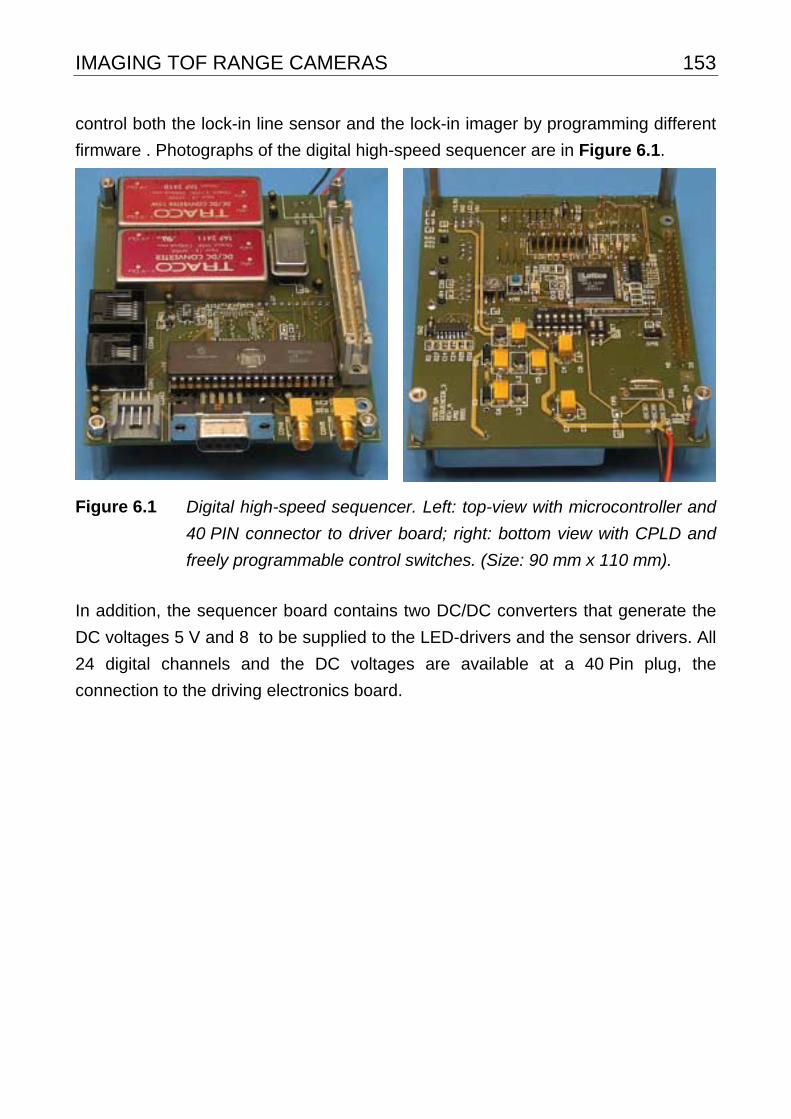
IMAGING TOF RANGE CAMERAS 153
control both the lock-in line sensor and the lock-in imager by programming different
firmware . Photographs of the digital high-speed sequencer are in Figure 6.1.
Figure 6.1 Digital high-speed sequencer. Left: top-view with microcontroller and
40 PIN connector to driver board; right: bottom view with CPLD and
freely programmable control switches. (Size: 90 mm x 110 mm).
In addition, the sequencer board contains two DC/DC converters that generate the
DC voltages 5 V and 8 to be supplied to the LED-drivers and the sensor drivers. All
24 digital channels and the DC voltages are available at a 40 Pin plug, the
connection to the driving electronics board.
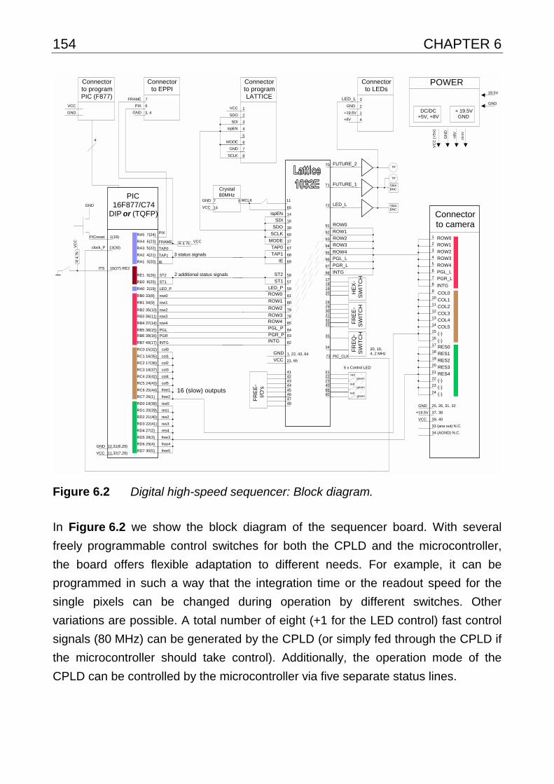
154 CHAPTER 6
Connector to camera
1
2
3
4
5
6
7
8
9
10
11
12
13
14
15
16
17
18
19
20
21
22
23
24
25, 26, 31, 32
37, 38
39, 40
33 (ana out) N.C.
34 (AGND) N.C.
VCC
+19.5V
GND
Connector to EPPI
FRAME
PIX
GND
7
6
3, 4 DC/DC+5V, +8V
+ 19.5VGND
POWERConnector to programLATTICE
1
2
3
4
5
ispEN
SDI
SDO
SCLK
6MODE
7
8
VCC
GND
65
14
16
39
60
37
67
68
69
58
59
TAP0
TAP1
IE
ST2
LED_P
ispEN
SDI
SDO
SCLK
MODE
91
92
93
94
95
96
97
98
ROW0
ROW1
ROW2
ROW3
ROW4
PGL_L
PGR_L
INTG
72
35
34
LED_L
1, 22, 43, 64
21, 65
GND
VCC
PIC16F877/C74
DIP or (TQFP)
RC0 15(32)
FRAME
RA3 5(22)
RA2 4(21)
RA1 3(20)
10(27) RE2
RE1 9(26)
RE0 8(25)
RA0 2(19)
16 (slow) outputs
3 status signals
clock_P
RA4 6(23)
13(30)
2 additional status signals
RA5 7(24) PIX
TAP0
TAP1
IE
LED_P
78ROW3RB3 36(11) row3
ST1
ST2
ITS
RC1 16(35)
RC2 17(36)
RC3 18(37)
RC4 23(42)
RC5 24(43)
RC6 25(44)
RC7 26(1)
RD0 19(38)
RD1 20(39)
RD2 21(40)
RD3 22(41)
RD4 27(2)
RD5 28(3)
RD6 29(4)
RD7 30(5)
free1
col5
col4
col3
col2
col1
col0
VCC
GND
11,32(7,28)
12,31(6,29)
VCCR 4.7k
1(18)PICreset
GND
Connector to LEDs
LED_L
1
GND
+19.5V
2
3
FR
EQ
-S
WIT
CH
Crystal80MHz
7
14
8 MCLKGND
VCC
VC
C (
+5
V)
GN
D
+8
V
19.5V
GND
19.5
V
4+8V
PIC_CLK73
20, 10,4, 2 MHz
VC
CR
4.7
k
11
71 FUTURE_1
70 FUTURE_2
SMABNC
SMABNC
TP
3132 F
RE
E-
SW
ITC
H
3029
1920 H
EX
-S
WIT
CH
1817
33
28
4086
2322
90
216 x Control LED
red
red
red
green
green
green
Connector to programPIC (F877)
4
VCC
GND
TP
4445
FR
EE
-I/O
's
4342
46
41
4748
res2
free4
free2
res1
res3
free3
res0
res4
free5
ST1 57
80ROW1RB1 34(9) row1
81ROW0RB0 33(8) row0
82INTGRB7 40(17) INTG
83PGR_PRB6 39(16) PGR
84PGL_PRB5 38(15) PGL
85ROW4RB4 37(14) row4
79ROW2RB2 35(10) row2
ROW0
ROW1
ROW2
ROW3
ROW4
PGL_L
PGR_L
INTG
RES2
RES1
RES3
RES0
RES4
(-)
COL5
COL4
COL3
COL2
COL1
COL0
(-)
(-)
(-)
(-)
Figure 6.2 Digital high-speed sequencer: Block diagram.
In Figure 6.2 we show the block diagram of the sequencer board. With several
freely programmable control switches for both the CPLD and the microcontroller,
the board offers flexible adaptation to different needs. For example, it can be
programmed in such a way that the integration time or the readout speed for the
single pixels can be changed during operation by different switches. Other
variations are possible. A total number of eight (+1 for the LED control) fast control
signals (80 MHz) can be generated by the CPLD (or simply fed through the CPLD if
the microcontroller should take control). Additionally, the operation mode of the
CPLD can be controlled by the microcontroller via five separate status lines.
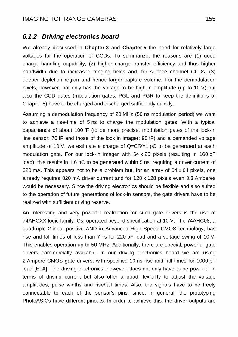
IMAGING TOF RANGE CAMERAS 155
6.1.2 Driving electronics board
We already discussed in Chapter 3 and Chapter 5 the need for relatively large
voltages for the operation of CCDs. To summarize, the reasons are (1) good
charge handling capability, (2) higher charge transfer efficiency and thus higher
bandwidth due to increased fringing fields and, for surface channel CCDs, (3)
deeper depletion region and hence larger capture volume. For the demodulation
pixels, however, not only has the voltage to be high in amplitude (up to 10 V) but
also the CCD gates (modulation gates, PGL and PGR to keep the definitions of
Chapter 5) have to be charged and discharged sufficiently quickly.
Assuming a demodulation frequency of 20 MHz (50 ns modulation period) we want
to achieve a rise-time of 5 ns to charge the modulation gates. With a typical
capacitance of about 100 fF (to be more precise, modulation gates of the lock-in
line sensor: 70 fF and those of the lock in imager: 90 fF) and a demanded voltage
amplitude of 10 V, we estimate a charge of Q=C⋅V=1 pC to be generated at each
modulation gate. For our lock-in imager with 64 x 25 pixels (resulting in 160 pF
load), this results in 1.6 nC to be generated within 5 ns, requiring a driver current of
320 mA. This appears not to be a problem but, for an array of 64 x 64 pixels, one
already requires 820 mA driver current and for 128 x 128 pixels even 3.3 Amperes
would be necessary. Since the driving electronics should be flexible and also suited
to the operation of future generations of lock-in sensors, the gate drivers have to be
realized with sufficient driving reserve.
An interesting and very powerful realization for such gate drivers is the use of
74AHCXX logic family ICs, operated beyond specification at 10 V. The 74AHC08, a
quadruple 2-input positive AND in Advanced High Speed CMOS technology, has
rise and fall times of less than 7 ns for 220 pF load and a voltage swing of 10 V.
This enables operation up to 50 MHz. Additionally, there are special, powerful gate
drivers commercially available. In our driving electronics board we are using
2 Ampere CMOS gate drivers, with specified 10 ns rise and fall times for 1000 pF
load [ELA]. The driving electronics, however, does not only have to be powerful in
terms of driving current but also offer a good flexibility to adjust the voltage
amplitudes, pulse widths and rise/fall times. Also, the signals have to be freely
connectable to each of the sensor’s pins, since, in general, the prototyping
PhotoASICs have different pinouts. In order to achieve this, the driver outputs are
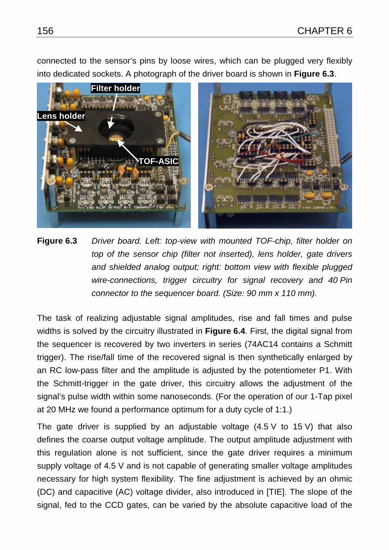
156 CHAPTER 6
connected to the sensor’s pins by loose wires, which can be plugged very flexibly
into dedicated sockets. A photograph of the driver board is shown in Figure 6.3.
Lens holder
Filter holder
TOF-ASIC
Figure 6.3 Driver board. Left: top-view with mounted TOF-chip, filter holder on
top of the sensor chip (filter not inserted), lens holder, gate drivers
and shielded analog output; right: bottom view with flexible plugged
wire-connections, trigger circuitry for signal recovery and 40 Pin
connector to the sequencer board. (Size: 90 mm x 110 mm).
The task of realizing adjustable signal amplitudes, rise and fall times and pulse
widths is solved by the circuitry illustrated in Figure 6.4. First, the digital signal from
the sequencer is recovered by two inverters in series (74AC14 contains a Schmitt
trigger). The rise/fall time of the recovered signal is then synthetically enlarged by
an RC low-pass filter and the amplitude is adjusted by the potentiometer P1. With
the Schmitt-trigger in the gate driver, this circuitry allows the adjustment of the
signal’s pulse width within some nanoseconds. (For the operation of our 1-Tap pixel
at 20 MHz we found a performance optimum for a duty cycle of 1:1.)
The gate driver is supplied by an adjustable voltage (4.5 V to 15 V) that also
defines the coarse output voltage amplitude. The output amplitude adjustment with
this regulation alone is not sufficient, since the gate driver requires a minimum
supply voltage of 4.5 V and is not capable of generating smaller voltage amplitudes
necessary for high system flexibility. The fine adjustment is achieved by an ohmic
(DC) and capacitive (AC) voltage divider, also introduced in [TIE]. The slope of the
signal, fed to the CCD gates, can be varied by the absolute capacitive load of the
IMAGING TOF RANGE CAMERAS 157
gate drivers (CCD load plus load capacitors) on the camera board. This rise/fall
time of the CCD gate signals influences the efficiency of the charge transfer (c.f.
[SP4]) and the effective ON/OFF shutter ratio of the demodulation pixels.
Gatedriver
22Ω
to CCD gate
C1
C2
P2: 1kΩ
LM317voltageregulator
4.5 V - 15 Vdriver supply
voltage
10Ω
74AC14330Ω
P1: 2kΩ
15p
digital TTLsignal fromsequencer
0 V
5 V
0 V
5 V
200Ω
0 V
trigger level of gate driver
I
II III IV
V
I
II
III
IV
V
0 V
Signal recovery
Coarse amplitude adjustment Amplitude fine tuningand
Adjustment of rise/fall time
Pulse width adjustment
Coarse amplitude
DC and AC fine tuned driving signal
P1
P2, C1/C2,coarse voltage slope:
C1 + C2
Figure 6.4 Driver circuitry including signal recovery (I, II), pulse width
adjustment (III, IV), coarse amplitude adjustment (IV) and fine
amplitude tuning (V). For the fine-tuning of the signal amplitude a
capacitive (AC) and ohmic (DC) voltage divider is used. The
dimensions of these capacitors and resistors determine the signal
slope. (RC low-pass).
The driver board illustrated in Figure 6.3 contains 24 separate CCD driver
channels. Eight of these channels offer the above described pulse width and signal
slope adjustment. The remaining 16 channels can be adjusted in amplitude by the
coarse amplitude setting of the gate drivers and in signal slope by an additional
capacitive load. For high flexibility, the discrete capacitors are plugged into sockets
rather than being soldered (c.f. Figure 6.3 left). In addition, nine different DC
signals can be provided to the PhotoASIC, four of which are targeted for use as
158 CHAPTER 6
power supplies (1.25 V to 11.7 V with up to 40 mA each) and five DC channels to
be used as fixed gate bias voltages (0 V to 13 V DC, 10 µA maximum).
Figure 6.3 also shows the lens holder and the holder for an interference filter (filter
not mounted in the photograph). We use an EALING interference filter (42-7344)
with 633 nm center-wavelength and 38 nm half-intensity-bandwidth (HBW). The
mean filter transmission within the HBW is about 75 %. The interference filter is
used to suppress background illumination by transmitting only the spectrum of the
LED illumination used.
6.1.3 Modulated illumination
As modulated light source we use LEDs arranged in arrays (LED line for the line
sensor and 2D LED-array for the TOF imager). Because of its excellent optical
output power we use the Hewlett Packard (now Agilent) HPWT DH00 LEDs. They
emit at a center wavelength of 630 nm with a spectral bandwidth of about 35 nm
(FMHW) and a beam divergence of typically ± 25°. The optical output power
(specified as luminous flux) depends on the LED category. It is specified with 2.5
lumens (10 mW) for the D-category LEDs that we use for the 2D camera [HP1,
HP2]. The LEDs are driven by a special current-protected and stabilized fast
switching driving electronics developed at CSEM.
In the Appendix we give the equations to calculate the optical power in terms of
watts from the luminous flux in terms of lumens, depending on the wavelength. The
measured optical power of the LEDs we use in our illumination modules is 8.5 mW
@ 50 mA for the line camera and 5 mW @ 50 mA for the 3D camera. For the 3D
camera, we unfortunately only received LEDs of lower power category from our
distributor.
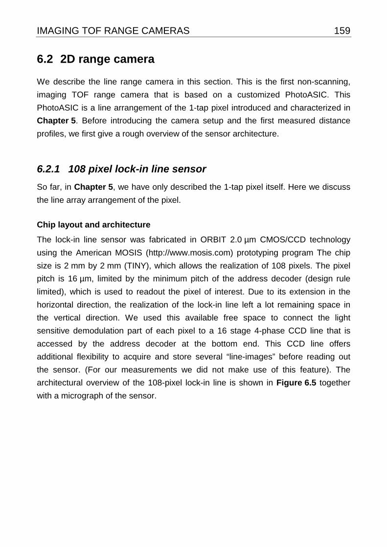
IMAGING TOF RANGE CAMERAS 159
6.2 2D range camera
We describe the line range camera in this section. This is the first non-scanning,
imaging TOF range camera that is based on a customized PhotoASIC. This
PhotoASIC is a line arrangement of the 1-tap pixel introduced and characterized in
Chapter 5. Before introducing the camera setup and the first measured distance
profiles, we first give a rough overview of the sensor architecture.
6.2.1 108 pixel lock-in line sensor
So far, in Chapter 5, we have only described the 1-tap pixel itself. Here we discuss
the line array arrangement of the pixel.
Chip layout and architecture
The lock-in line sensor was fabricated in ORBIT 2.0 µm CMOS/CCD technology
using the American MOSIS (http://www.mosis.com) prototyping program The chip
size is 2 mm by 2 mm (TINY), which allows the realization of 108 pixels. The pixel
pitch is 16 µm, limited by the minimum pitch of the address decoder (design rule
limited), which is used to readout the pixel of interest. Due to its extension in the
horizontal direction, the realization of the lock-in line left a lot remaining space in
the vertical direction. We used this available free space to connect the light
sensitive demodulation part of each pixel to a 16 stage 4-phase CCD line that is
accessed by the address decoder at the bottom end. This CCD line offers
additional flexibility to acquire and store several “line-images” before reading out
the sensor. (For our measurements we did not make use of this feature). The
architectural overview of the 108-pixel lock-in line is shown in Figure 6.5 together
with a micrograph of the sensor.
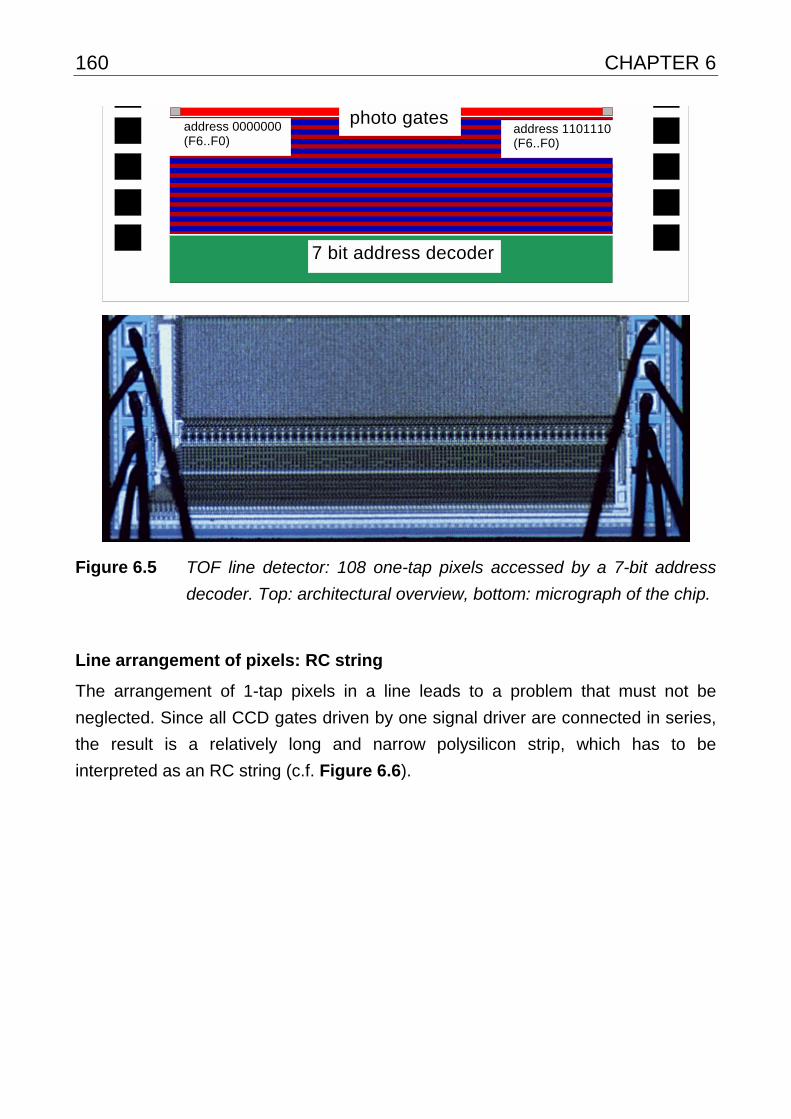
160 CHAPTER 6
photo gates
7 bit address decoder
address 0000000(F6..F0)
address 1101110(F6..F0)
Figure 6.5 TOF line detector: 108 one-tap pixels accessed by a 7-bit address
decoder. Top: architectural overview, bottom: micrograph of the chip.
Line arrangement of pixels: RC string
The arrangement of 1-tap pixels in a line leads to a problem that must not be
neglected. Since all CCD gates driven by one signal driver are connected in series,
the result is a relatively long and narrow polysilicon strip, which has to be
interpreted as an RC string (c.f. Figure 6.6).
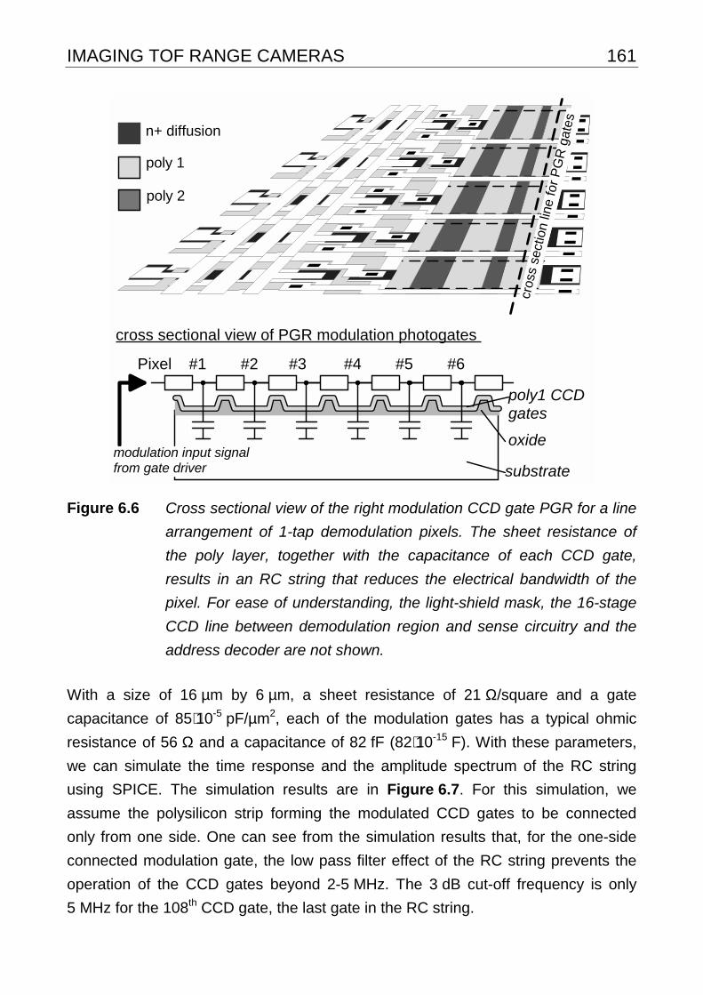
IMAGING TOF RANGE CAMERAS 161
n+ diffusion
poly 2
poly 1
Pixel #1 #2 #3 #4 #5 #6
modulation input signal from gate driver
cross sectional view of PGR modulation photogates
cros
s se
ctio
n lin
e fo
r P
GR
gat
es
oxide
substrate
poly1 CCDgates
Figure 6.6 Cross sectional view of the right modulation CCD gate PGR for a line
arrangement of 1-tap demodulation pixels. The sheet resistance of
the poly layer, together with the capacitance of each CCD gate,
results in an RC string that reduces the electrical bandwidth of the
pixel. For ease of understanding, the light-shield mask, the 16-stage
CCD line between demodulation region and sense circuitry and the
address decoder are not shown.
With a size of 16 µm by 6 µm, a sheet resistance of 21 Ω/square and a gate
capacitance of 85⋅10-5 pF/µm2, each of the modulation gates has a typical ohmic
resistance of 56 Ω and a capacitance of 82 fF (82⋅10-15 F). With these parameters,
we can simulate the time response and the amplitude spectrum of the RC string
using SPICE. The simulation results are in Figure 6.7. For this simulation, we
assume the polysilicon strip forming the modulated CCD gates to be connected
only from one side. One can see from the simulation results that, for the one-side
connected modulation gate, the low pass filter effect of the RC string prevents the
operation of the CCD gates beyond 2-5 MHz. The 3 dB cut-off frequency is only
5 MHz for the 108th CCD gate, the last gate in the RC string.
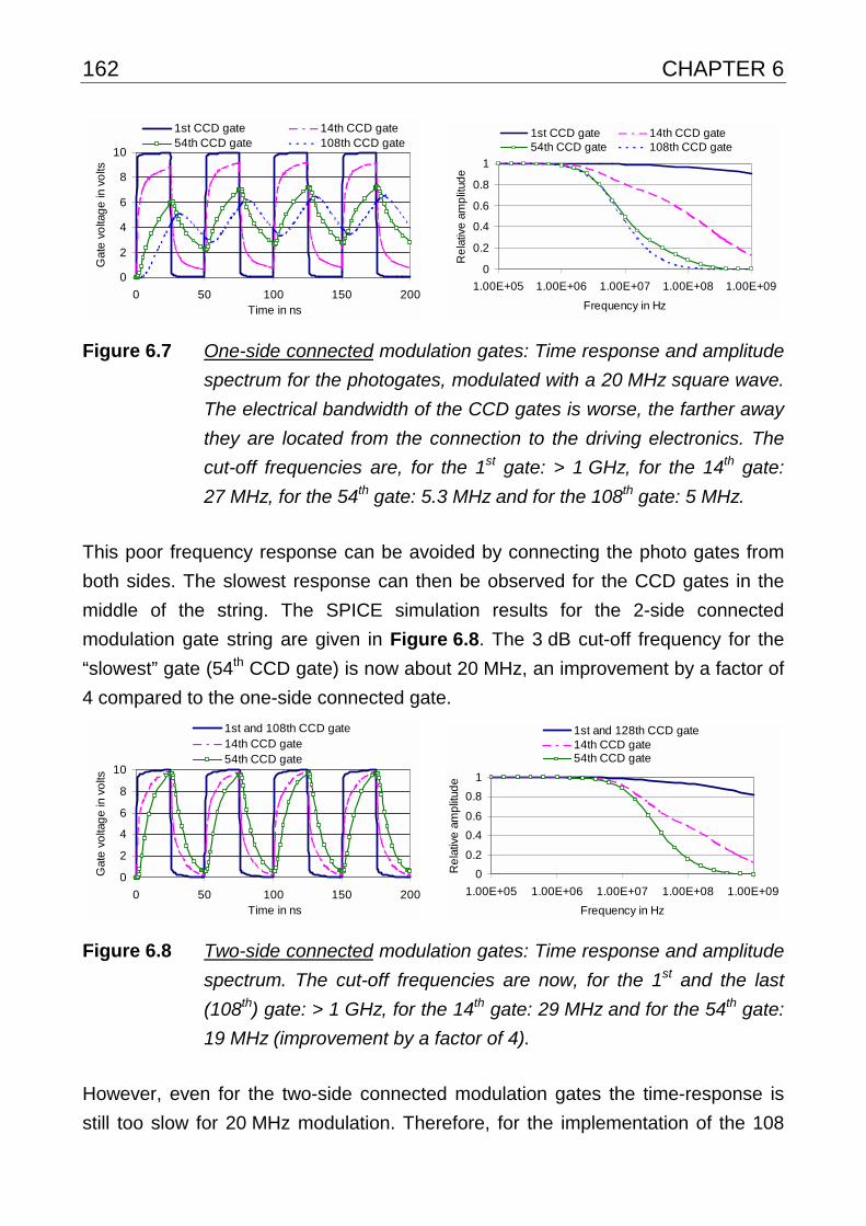
162 CHAPTER 6
0
2
4
6
8
10
0 50 100 150 200Time in ns
Gat
e v
olta
ge
in v
olts
1st CCD gate 14th CCD gate54th CCD gate 108th CCD gate
0
0.2
0.4
0.6
0.8
1
1.00E+05 1.00E+06 1.00E+07 1.00E+08 1.00E+09
Frequency in Hz
Re
lativ
e a
mp
litud
e
1st CCD gate 14th CCD gate54th CCD gate 108th CCD gate
Figure 6.7 One-side connected modulation gates: Time response and amplitude
spectrum for the photogates, modulated with a 20 MHz square wave.
The electrical bandwidth of the CCD gates is worse, the farther away
they are located from the connection to the driving electronics. The
cut-off frequencies are, for the 1st gate: > 1 GHz, for the 14th gate:
27 MHz, for the 54th gate: 5.3 MHz and for the 108th gate: 5 MHz.
This poor frequency response can be avoided by connecting the photo gates from
both sides. The slowest response can then be observed for the CCD gates in the
middle of the string. The SPICE simulation results for the 2-side connected
modulation gate string are given in Figure 6.8. The 3 dB cut-off frequency for the
“slowest” gate (54th CCD gate) is now about 20 MHz, an improvement by a factor of
4 compared to the one-side connected gate.
0
2
4
6
8
10
0 50 100 150 200Time in ns
Gat
e v
olta
ge
in v
olts
1st and 108th CCD gate14th CCD gate54th CCD gate
0
0.2
0.4
0.6
0.8
1
1.00E+05 1.00E+06 1.00E+07 1.00E+08 1.00E+09
Frequency in Hz
Re
lativ
e a
mp
litud
e
1st and 128th CCD gate14th CCD gate54th CCD gate
Figure 6.8 Two-side connected modulation gates: Time response and amplitude
spectrum. The cut-off frequencies are now, for the 1st and the last
(108th) gate: > 1 GHz, for the 14th gate: 29 MHz and for the 54th gate:
19 MHz (improvement by a factor of 4).
However, even for the two-side connected modulation gates the time-response is
still too slow for 20 MHz modulation. Therefore, for the implementation of the 108
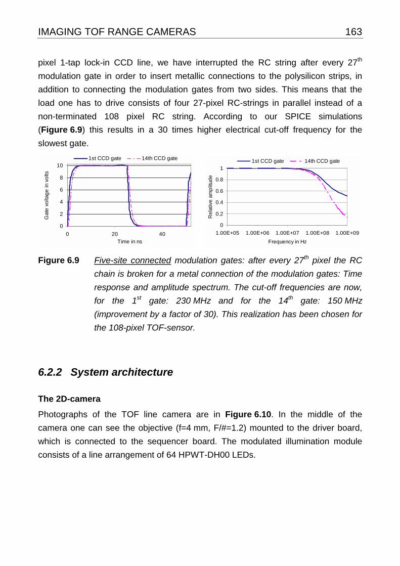
IMAGING TOF RANGE CAMERAS 163
pixel 1-tap lock-in CCD line, we have interrupted the RC string after every 27th
modulation gate in order to insert metallic connections to the polysilicon strips, in
addition to connecting the modulation gates from two sides. This means that the
load one has to drive consists of four 27-pixel RC-strings in parallel instead of a
non-terminated 108 pixel RC string. According to our SPICE simulations
(Figure 6.9) this results in a 30 times higher electrical cut-off frequency for the
slowest gate.
0
2
4
6
8
10
0 20 40
Time in ns
Gat
e v
olta
ge
in v
olts
1st CCD gate 14th CCD gate
0
0.2
0.4
0.6
0.8
1
1.00E+05 1.00E+06 1.00E+07 1.00E+08 1.00E+09
Frequency in Hz
Re
lativ
e a
mp
litud
e
1st CCD gate 14th CCD gate
Figure 6.9 Five-site connected modulation gates: after every 27th pixel the RC
chain is broken for a metal connection of the modulation gates: Time
response and amplitude spectrum. The cut-off frequencies are now,
for the 1st gate: 230 MHz and for the 14th gate: 150 MHz
(improvement by a factor of 30). This realization has been chosen for
the 108-pixel TOF-sensor.
6.2.2 System architecture
The 2D-camera
Photographs of the TOF line camera are in Figure 6.10. In the middle of the
camera one can see the objective (f=4 mm, F/#=1.2) mounted to the driver board,
which is connected to the sequencer board. The modulated illumination module
consists of a line arrangement of 64 HPWT-DH00 LEDs.
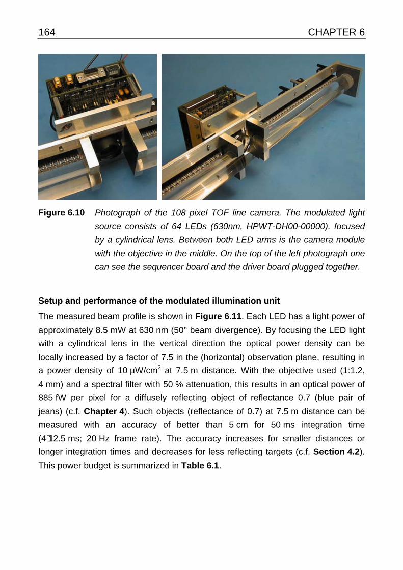
164 CHAPTER 6
Figure 6.10 Photograph of the 108 pixel TOF line camera. The modulated light
source consists of 64 LEDs (630nm, HPWT-DH00-00000), focused
by a cylindrical lens. Between both LED arms is the camera module
with the objective in the middle. On the top of the left photograph one
can see the sequencer board and the driver board plugged together.
Setup and performance of the modulated illumination unit
The measured beam profile is shown in Figure 6.11. Each LED has a light power of
approximately 8.5 mW at 630 nm (50° beam divergence). By focusing the LED light
with a cylindrical lens in the vertical direction the optical power density can be
locally increased by a factor of 7.5 in the (horizontal) observation plane, resulting in
a power density of 10 µW/cm2 at 7.5 m distance. With the objective used (1:1.2,
4 mm) and a spectral filter with 50 % attenuation, this results in an optical power of
885 fW per pixel for a diffusely reflecting object of reflectance 0.7 (blue pair of
jeans) (c.f. Chapter 4). Such objects (reflectance of 0.7) at 7.5 m distance can be
measured with an accuracy of better than 5 cm for 50 ms integration time
(4⋅12.5 ms; 20 Hz frame rate). The accuracy increases for smaller distances or
longer integration times and decreases for less reflecting targets (c.f. Section 4.2).
This power budget is summarized in Table 6.1.
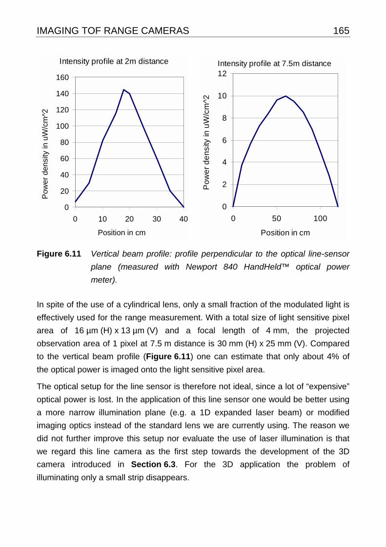
IMAGING TOF RANGE CAMERAS 165
Intensity profile at 2m distance
0
20
40
60
80
100
120
140
160
0 10 20 30 40
Position in cm
Pow
er
densi
ty in
uW
/cm
^2
Intensity profile at 7.5m distance
0
2
4
6
8
10
12
0 50 100
Position in cm
Po
we
r d
en
sity
in u
W/c
m^2
Figure 6.11 Vertical beam profile: profile perpendicular to the optical line-sensor
plane (measured with Newport 840 HandHeld™ optical power
meter).
In spite of the use of a cylindrical lens, only a small fraction of the modulated light is
effectively used for the range measurement. With a total size of light sensitive pixel
area of 16 µm (H) x 13 µm (V) and a focal length of 4 mm, the projected
observation area of 1 pixel at 7.5 m distance is 30 mm (H) x 25 mm (V). Compared
to the vertical beam profile (Figure 6.11) one can estimate that only about 4% of
the optical power is imaged onto the light sensitive pixel area.
The optical setup for the line sensor is therefore not ideal, since a lot of “expensive”
optical power is lost. In the application of this line sensor one would be better using
a more narrow illumination plane (e.g. a 1D expanded laser beam) or modified
imaging optics instead of the standard lens we are currently using. The reason we
did not further improve this setup nor evaluate the use of laser illumination is that
we regard this line camera as the first step towards the development of the 3D
camera introduced in Section 6.3. For the 3D application the problem of
illuminating only a small strip disappears.
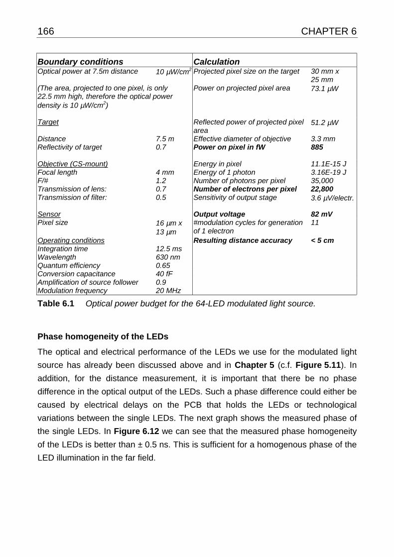
166 CHAPTER 6
Boundary conditions Calculation Optical power at 7.5m distance 10 µW/cm2 Projected pixel size on the target 30 mm x
25 mm (The area, projected to one pixel, is only 22.5 mm high, therefore the optical power density is 10 µW/cm2)
Power on projected pixel area 73.1 µW
Target Reflected power of projected pixel area
51.2 µW
Distance 7.5 m Effective diameter of objective 3.3 mm Reflectivity of target
0.7 Power on pixel in fW 885
Objective (CS-mount) Energy in pixel 11.1E-15 J Focal length 4 mm Energy of 1 photon 3.16E-19 J F/# 1.2 Number of photons per pixel 35,000 Transmission of lens: 0.7 Number of electrons per pixel 22,800 Transmission of filter:
0.5 Sensitivity of output stage 3.6 µV/electr.
Sensor Output voltage 82 mV Pixel size
16 µm x 13 µm
#modulation cycles for generation of 1 electron
11
Operating conditions Resulting distance accuracy < 5 cm Integration time 12.5 ms Wavelength 630 nm Quantum efficiency 0.65 Conversion capacitance 40 fF Amplification of source follower 0.9 Modulation frequency 20 MHz
Table 6.1 Optical power budget for the 64-LED modulated light source.
Phase homogeneity of the LEDs
The optical and electrical performance of the LEDs we use for the modulated light
source has already been discussed above and in Chapter 5 (c.f. Figure 5.11). In
addition, for the distance measurement, it is important that there be no phase
difference in the optical output of the LEDs. Such a phase difference could either be
caused by electrical delays on the PCB that holds the LEDs or technological
variations between the single LEDs. The next graph shows the measured phase of
the single LEDs. In Figure 6.12 we can see that the measured phase homogeneity
of the LEDs is better than ± 0.5 ns. This is sufficient for a homogenous phase of the
LED illumination in the far field.
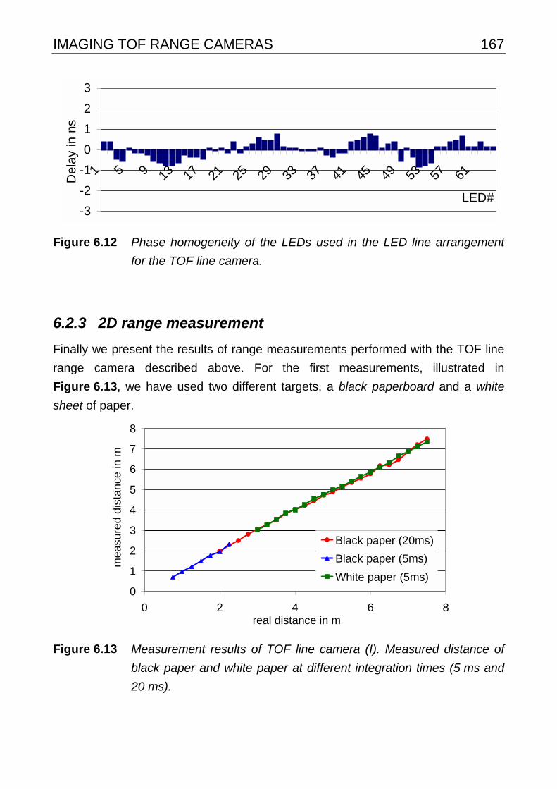
IMAGING TOF RANGE CAMERAS 167
-3
-2
-1
0
1
2
3
1 5 9 13 17 21 25 29 33 37 41 45 49 53 57 61
LED#
De
lay
in n
s
Figure 6.12 Phase homogeneity of the LEDs used in the LED line arrangement
for the TOF line camera.
6.2.3 2D range measurement
Finally we present the results of range measurements performed with the TOF line
range camera described above. For the first measurements, illustrated in
Figure 6.13, we have used two different targets, a black paperboard and a white
sheet of paper.
0
1
2
3
4
5
6
7
8
0 2 4 6 8real distance in m
me
asu
red
dis
tan
ce in
m
Black paper (20ms)
Black paper (5ms)
White paper (5ms)
Figure 6.13 Measurement results of TOF line camera (I). Measured distance of
black paper and white paper at different integration times (5 ms and
20 ms).
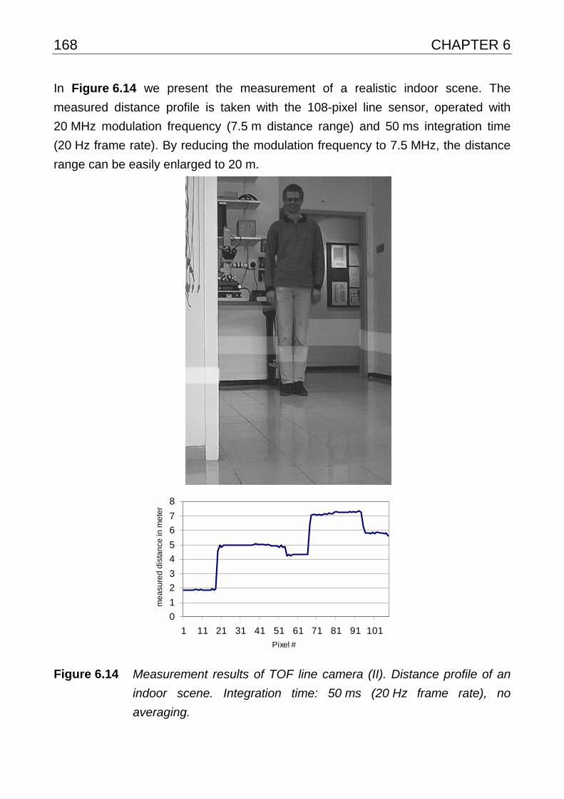
168 CHAPTER 6
In Figure 6.14 we present the measurement of a realistic indoor scene. The
measured distance profile is taken with the 108-pixel line sensor, operated with
20 MHz modulation frequency (7.5 m distance range) and 50 ms integration time
(20 Hz frame rate). By reducing the modulation frequency to 7.5 MHz, the distance
range can be easily enlarged to 20 m.
0
1
2
3
4
5
6
7
8
1 11 21 31 41 51 61 71 81 91 101
Pixel #
me
asu
red
dis
tan
ce in
me
ter
Figure 6.14 Measurement results of TOF line camera (II). Distance profile of an
indoor scene. Integration time: 50 ms (20 Hz frame rate), no
averaging.
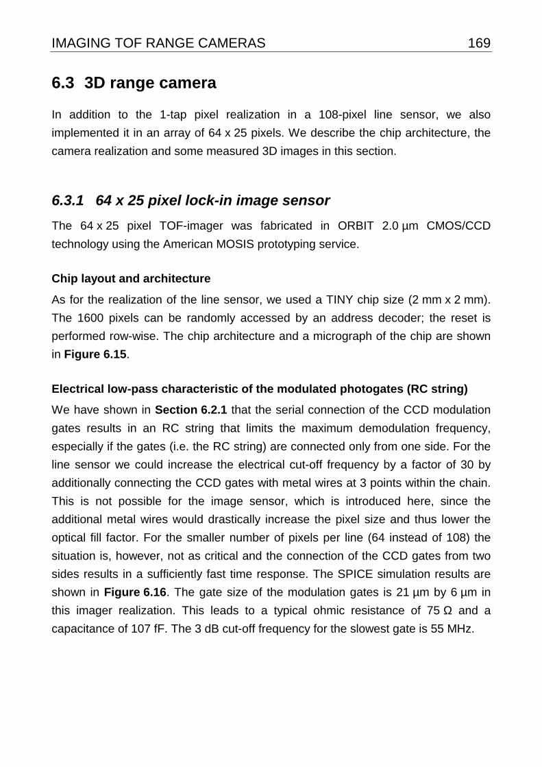
IMAGING TOF RANGE CAMERAS 169
6.3 3D range camera
In addition to the 1-tap pixel realization in a 108-pixel line sensor, we also
implemented it in an array of 64 x 25 pixels. We describe the chip architecture, the
camera realization and some measured 3D images in this section.
6.3.1 64 x 25 pixel lock-in image sensor
The 64 x 25 pixel TOF-imager was fabricated in ORBIT 2.0 µm CMOS/CCD
technology using the American MOSIS prototyping service.
Chip layout and architecture
As for the realization of the line sensor, we used a TINY chip size (2 mm x 2 mm).
The 1600 pixels can be randomly accessed by an address decoder; the reset is
performed row-wise. The chip architecture and a micrograph of the chip are shown
in Figure 6.15.
Electrical low-pass characteristic of the modulated photogates (RC string)
We have shown in Section 6.2.1 that the serial connection of the CCD modulation
gates results in an RC string that limits the maximum demodulation frequency,
especially if the gates (i.e. the RC string) are connected only from one side. For the
line sensor we could increase the electrical cut-off frequency by a factor of 30 by
additionally connecting the CCD gates with metal wires at 3 points within the chain.
This is not possible for the image sensor, which is introduced here, since the
additional metal wires would drastically increase the pixel size and thus lower the
optical fill factor. For the smaller number of pixels per line (64 instead of 108) the
situation is, however, not as critical and the connection of the CCD gates from two
sides results in a sufficiently fast time response. The SPICE simulation results are
shown in Figure 6.16. The gate size of the modulation gates is 21 µm by 6 µm in
this imager realization. This leads to a typical ohmic resistance of 75 Ω and a
capacitance of 107 fF. The 3 dB cut-off frequency for the slowest gate is 55 MHz.
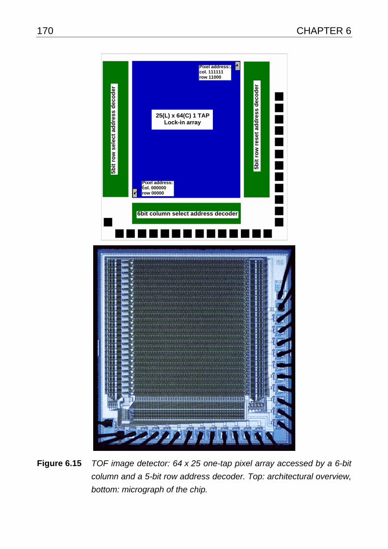
170 CHAPTER 6
6bit column select address decoder
5b
it r
ow
re
se
t a
dd
res
s d
ec
od
er
5b
it r
ow
se
lec
t a
dd
res
s d
ec
od
er
25(L) x 64(C) 1 TAP Lock-in array
Pixel address:col. 000000row 00000
Pixel address:col. 111111row 11000
Figure 6.15
TOF image detector: 64 x 25 one-tap pixel array accessed by a 6-bit
column and a 5-bit row address decoder. Top: architectural overview,
bottom: micrograph of the chip.
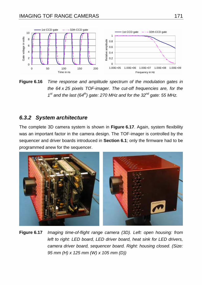
IMAGING TOF RANGE CAMERAS 171
0
2
4
6
8
10
0 50 100 150 200Time in ns
Gat
e v
olta
ge
in v
olts
1st CCD gate 32th CCD gate
0
0.2
0.4
0.6
0.8
1
1.00E+05 1.00E+06 1.00E+07 1.00E+08 1.00E+09
Frequency in Hz
Re
lativ
e a
mp
litud
e
1st CCD gate 32th CCD gate
Figure 6.16 Time response and amplitude spectrum of the modulation gates in
the 64 x 25 pixels TOF-imager. The cut-off frequencies are, for the
1st and the last (64th) gate: 270 MHz and for the 32nd gate: 55 MHz.
6.3.2 System architecture
The complete 3D camera system is shown in Figure 6.17. Again, system flexibility
was an important factor in the camera design. The TOF-imager is controlled by the
sequencer and driver boards introduced in Section 6.1; only the firmware had to be
programmed anew for the sequencer.
Figure 6.17 Imaging time-of-flight range camera (3D). Left: open housing: from
left to right: LED board, LED driver board, heat sink for LED drivers,
camera driver board, sequencer board. Right: housing closed. (Size:
95 mm (H) x 125 mm (W) x 105 mm (D))
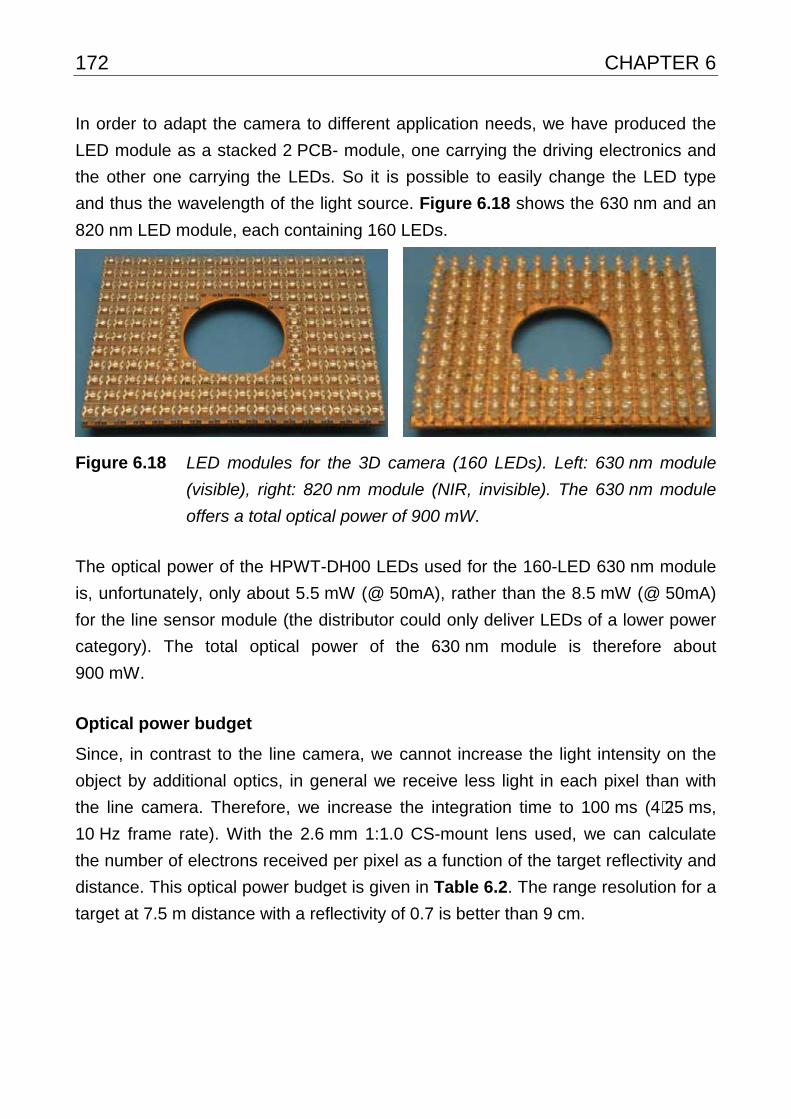
172 CHAPTER 6
In order to adapt the camera to different application needs, we have produced the
LED module as a stacked 2 PCB- module, one carrying the driving electronics and
the other one carrying the LEDs. So it is possible to easily change the LED type
and thus the wavelength of the light source. Figure 6.18 shows the 630 nm and an
820 nm LED module, each containing 160 LEDs.
Figure 6.18 LED modules for the 3D camera (160 LEDs). Left: 630 nm module
(visible), right: 820 nm module (NIR, invisible). The 630 nm module
offers a total optical power of 900 mW.
The optical power of the HPWT-DH00 LEDs used for the 160-LED 630 nm module
is, unfortunately, only about 5.5 mW (@ 50mA), rather than the 8.5 mW (@ 50mA)
for the line sensor module (the distributor could only deliver LEDs of a lower power
category). The total optical power of the 630 nm module is therefore about
900 mW.
Optical power budget
Since, in contrast to the line camera, we cannot increase the light intensity on the
object by additional optics, in general we receive less light in each pixel than with
the line camera. Therefore, we increase the integration time to 100 ms (4⋅25 ms,
10 Hz frame rate). With the 2.6 mm 1:1.0 CS-mount lens used, we can calculate
the number of electrons received per pixel as a function of the target reflectivity and
distance. This optical power budget is given in Table 6.2. The range resolution for a
target at 7.5 m distance with a reflectivity of 0.7 is better than 9 cm.
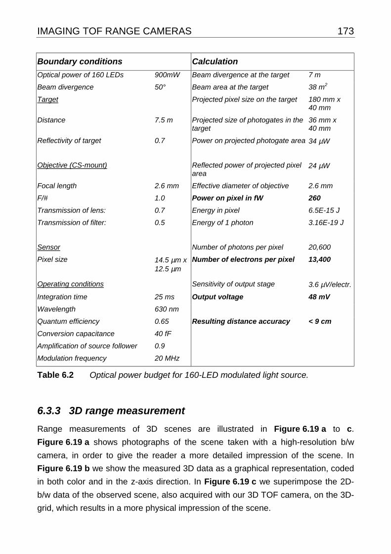
IMAGING TOF RANGE CAMERAS 173
Boundary conditions Calculation
Optical power of 160 LEDs 900mW Beam divergence at the target 7 m
Beam divergence 50° Beam area at the target 38 m2
Target Projected pixel size on the target 180 mm x 40 mm
Distance 7.5 m Projected size of photogates in the target
36 mm x 40 mm
Reflectivity of target
0.7 Power on projected photogate area 34 µW
Objective (CS-mount) Reflected power of projected pixel area
24 µW
Focal length 2.6 mm Effective diameter of objective 2.6 mm
F/# 1.0 Power on pixel in fW 260
Transmission of lens: 0.7 Energy in pixel 6.5E-15 J
Transmission of filter:
0.5 Energy of 1 photon 3.16E-19 J
Sensor Number of photons per pixel 20,600
Pixel size
14.5 µm x 12.5 µm
Number of electrons per pixel 13,400
Operating conditions Sensitivity of output stage 3.6 µV/electr.
Integration time 25 ms Output voltage 48 mV
Wavelength 630 nm
Quantum efficiency 0.65 Resulting distance accuracy < 9 cm
Conversion capacitance 40 fF
Amplification of source follower 0.9
Modulation frequency 20 MHz
Table 6.2 Optical power budget for 160-LED modulated light source.
6.3.3 3D range measurement
Range measurements of 3D scenes are illustrated in Figure 6.19 a to c.
Figure 6.19 a shows photographs of the scene taken with a high-resolution b/w
camera, in order to give the reader a more detailed impression of the scene. In
Figure 6.19 b we show the measured 3D data as a graphical representation, coded
in both color and in the z-axis direction. In Figure 6.19 c we superimpose the 2D-
b/w data of the observed scene, also acquired with our 3D TOF camera, on the 3D-
grid, which results in a more physical impression of the scene.
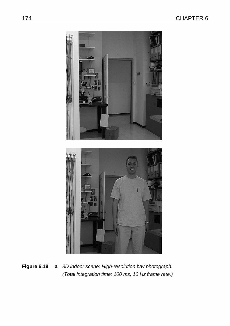
174 CHAPTER 6
Figure 6.19 a 3D indoor scene: High-resolution b/w photograph.
(Total integration time: 100 ms, 10 Hz frame rate.)
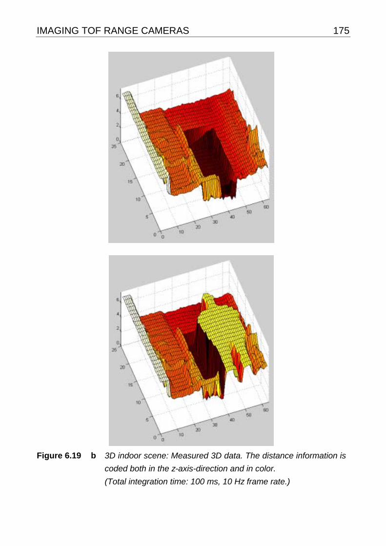
IMAGING TOF RANGE CAMERAS 175
Figure 6.19 b 3D indoor scene: Measured 3D data. The distance information is
coded both in the z-axis-direction and in color.
(Total integration time: 100 ms, 10 Hz frame rate.)
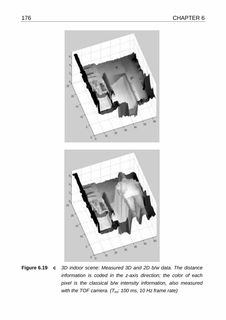
176 CHAPTER 6
Figure 6.19 c 3D indoor scene: Measured 3D and 2D b/w data. The distance
information is coded in the z-axis direction; the color of each
pixel is the classical b/w intensity information, also measured
with the TOF camera. (Tint: 100 ms, 10 Hz frame rate)

IMAGING TOF RANGE CAMERAS 177
Finally, Figure 6.20 shows an 8-frame sequence of range images acquired with our
3D TOF camera. The integration time for the acquisition of these range images was
100 ms for each measurement (10 Hz frame rate).
[FIGURES ON NEXT TWO PAGES]
Figure 6.20 Sequence of range images: A person approaching the 3D camera.
The distance information is coded in both the z-direction and color
(bright: close to the camera, dark: farther from the camera). The 2D
b/w images on the left-hand side have been taken with the 3D
camera simultaneously with the range images.
(Tint: 100 ms, 10 Hz frame rate)
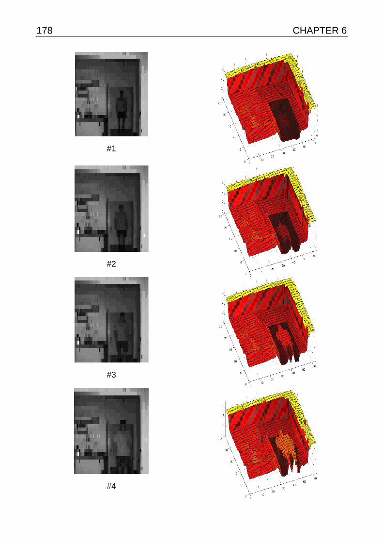
178 CHAPTER 6
#1
#2
#3
#4
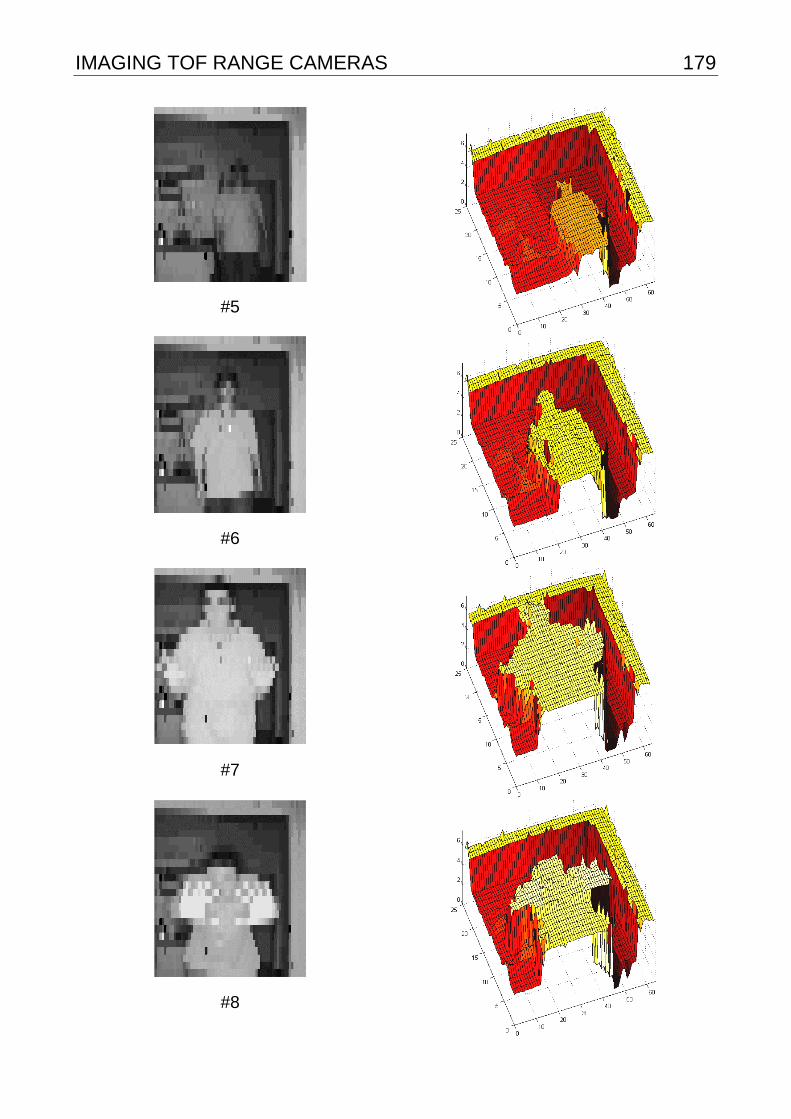
IMAGING TOF RANGE CAMERAS 179
#5
#6
#7
#8

180 CHAPTER 6
6.4 Discussion
With flexible implementations of a sequencer board and driving electronics suited
for CMOS/CCD circuitry we have built two TOF range cameras. These are the
world’s first all-solid-state 2D and 3D time-of-flight cameras that are based on
customized photoASICs. The arrangement of the 1-tap pixels in a line results in an
RC string that limits the modulation frequency for the modulated photogates. The
cut-off frequency can be increased by connecting the polysilicon strips from at least
two sides. It is thus possible to operate the range cameras at a modulation
frequency of 20 MHz, resulting in an unambiguous distance range of 7.5 meters.
Over the full distance range we can measure non-cooperative targets with an
accuracy of better than 10 centimeters. With the range measurements performed
we could affirm the ranging accuracy predicted in our estimations in Chapter 4.2.
SUMMARY AND PERSPECTIVE 181
7. Summary and Perspective
In this thesis we have presented the world’s first all-solid-state 3D time-of-flight
range camera that is based on a customized photoASIC and does not require any
mechanically moving parts. We achieve a distance resolution of a few centimeters
over the range of several meters at a frame rate of 10 Hz for non-cooperative
targets (reflectivity 0.7). The unambiguous distance range is 7.5 meters for 20 MHz
modulation frequency and 20 meters for a modulation frequency of 7.5 MHz.
We have given an overview of the existing range measurement techniques and
compared them to the time-of-flight method. Optical interferometry mainly targets
measurements in the range of several centimeters, and is therefore not a real
competitor in the 1-100 m range. The other popular ranging method, triangulation,
either active or passive, suffers from shadowing effects and requires a large
triangulation base and hence a large overall system size for good accuracy and
distance range.
Furthermore, we have described and compared the classical CCD image sensors
with CMOS APS imagers, which have gained more and more importance in recent
years. One of the “secrets” of this CMOS APS boom is that they can be fabricated
with standard technologies that are steadily being miniaturized and improved,
driven by the computer industry. This makes it possible to implement more and
more functionality within the sensor device and to realize more pixels on the same
silicon area. From the existing range measurement techniques the time-of-flight
method benefits most from this development in the semiconductor industry. While
all range measurement systems will more or less decrease in size (note:
triangulation will always require a large triangulation base for good accuracy), the
TOF method will additionally gain in measurement resolution. This is mainly
because the miniaturization in integrated circuits in general also leads to faster,
lower noise circuits and therefore improves the time- and thus distance-resolution
of TOF systems. For these reasons and in view of the additional advantages (no

182 CHAPTER 7
shadowing problems, compact setup) we are convinced that time-of-flight is the 3D-
measurement technique of the future.
To realize non-scanning 3D TOF cameras, an array of so-called demodulation
pixels is required. Each of the pixels in this array must have the functionality to
measure the arrival time of a modulated (optical) radiation field in addition to the
intensity. The task of measuring the time of flight can be solved by synchronously
sampling a periodically CW modulated optical signal. We have introduced such
“sampling” demodulation pixels of different architectures. Our pixels have been
implemented in a 2 µm CMOS/CCD technology. They make use of both the
advantages of a CMOS-APS, such as random pixel access, and also the
advantages of the CCD technique, which allows the addition of optically generated
charge carriers, essentially free of noise, and their movement and distribution into
defined storage areas in the semiconductor. We were able to show that, for a good
homogenous performance of the pixels, the light sensitive area (photogate) should
be accessed from only one (or two) site(s) since process inhomogeneities make it
impossible to achieve homogenous sampling point sensitivity for a four side
accessed photogate.
Especially since we use active illumination with the TOF method, the optical fill
factor of the pixels is of essential importance. The 1-tap pixel that we implemented
has an optical fill factor of 100% for the line sensor realization and 20% for the
realization as an image sensor. That is already competitive with CMOS APS
sensors. Additionally, the simple geometry of the light sensitive areas (lines of light
sensitive areas, i.e. 100% fill factor in one dimension and 20% in the other
dimension) makes it easy to realize and assemble highly efficient (cylindrical)
microlenses. For these simple structures microlenses can drastically improve the
optical fill factor (up to 100% for collimated light), so that, compared to our current
setup, either the optical power or the integration time can be reduced by a factor of
five. (For other photodetector arrays with asymmetrical photosites an efficient fill
factor improvement by microlenses is often a problem).
We have extensively characterized and described the demodulation performance of
the 1-tap pixel. For 20 MHz modulation frequency we measured a demodulation
contrast of 40 % for a 630 nm modulated light source. With a simple model we
could show that, even under DC conditions, the shutter efficiency of the pixel can
never be better than 60 % to 70 %, since a fraction of light always travels directly
SUMMARY AND PERSPECTIVE 183
into the storage area. Additionally, the more sinusoidal rather than square shaped
optical input signal at this frequency leads to an additional amplitude decrease so
that the final operation limit in terms of modulation frequency is still not reached at
20 MHz. The reason why we did not further increase the modulation frequency was
the limitation of the available control and driving electronics and also limitations of
the light source we used. The measured time or phase accuracy strongly depends
on the power of the modulated light and the integration time chosen for the signal
acquisition. For an integration time of 12.5 ms and an optical power of 750 fW, the
measured performance displays an accuracy of better than 250 picoseconds and
1.8 degrees respectively, resulting in a distance resolution of better than 4 cm. This
is a surprising performance, because the above mentioned optical power implies
that one electron is generated, statistically speaking, only every 13th modulation
period. This means that single electrons are moved, distributed and added in the
pixel with excellent reliability. The measured performance shows excellent fit to the
theoretical resolution predictions derived in Section 4.2. We are confident,
therefore, that we fully understand the relevant physical processes and their
influence on the distance resolution in any TOF ranging technique that relies on the
demodulation of modulated wave fields.
Based on the 1-tap demodulation pixel we have built two range cameras: one TOF
line camera (2D-range camera), working with the 108 pixel lock-in line sensor and
one 3D camera based on the 64 x 25 pixel lock-in imager. The measured range
accuracy is again in excellent agreement with our theoretical prediction. With the
3D camera we achieve a resolution of better than 10 cm for 100 ms integration time
(10 Hz) at 7.5 meters distance for non-cooperative targets of 70% reflectivity. The
range accuracy increases for shorter distances or longer integration times (more
optical energy). The range accuracy of the line camera is even better, since the
LED light can be focussed in one dimension, leading to an increase in optical power
density on the target. For this line sensor application, however, the illumination
setup and imaging optics can still be improved, since currently only about 5% of the
optically illuminated area is imaged on the pixels.
The drawback of serial sampling point acquisition of our current pixel realization,
that leads to measurement errors for quickly moving objects, can be overcome by a
new pixel structure described in Section 5.3. This solves the homogeneity problem
of accessing one light sensitive area within the pixel from four sides, as previously
184 CHAPTER 7
suggested, by using two optically identical photosites per pixel, both accessed from
two highly symmetrical sides. The “optical identity” can be achieved by a microlens
array that equally distributes and focuses the incoming optical power per pixel to
both photosites. With such a structure it will be possible to integrate all four
sampling points in parallel.
In the near future it will be possible to fabricate CCD structures in sub-micron
standard CMOS processes without any special CCD process option. This is
because, for smaller technologies, the minimum gap between two transistor gates
becomes so small that the potential barrier between these gates can be removed
with relatively low gate voltages of a few volts. The possibility to change from a
modified (non-standard) 2.0µm CMOS/CCD process, as we used for the pixels
presented here, to a standard CMOS process brings several advantages: (1) The
devices will become cheaper, (2) it will be possible for the first time to realize the
complete bandwidth of CCD signal processing combined with additional on-chip
functionality in a single process, and (3), it will be possible to realize smaller
structures. This is an enormous advantage, because the diffusion-limited transfer
time of charge carriers from one CCD gate to another increases with the square of
the CCD gate’s length. With smaller technologies, shorter gates become possible,
enabling a faster CCD transport. In particular, all of the pixels presented here will
be realizable even with improved performance in such a technology. First results of
such inter-poly-gap CCDs are presented in [CAR, FUR, HOP, KRA]. An interesting
but more demanding alternative to the 2D-demodulation device introduced here
would be the use of a sensitivity-modulated array of avalanche photodiodes. Such a
device is introduced in [BIB]; however, as long as the observed problems with too
high dark current and much too large excess noise factor are not solved, this
approach remains impractical.
To summarize, we have shown that TOF is the range imaging technique of the
future. We were able to demonstrate robust, compact range cameras (2D and 3D)
with excellent performance that is only limited in a very predictable manner by
ubiquitous quantum noise of the employed light. The ongoing miniaturization in
microelectronics will lead to faster demodulation devices so that we can expect
devices for demodulation frequencies beyond 100 MHz in the future. Also, it will be
possible to realize additional functionality such as on-chip A/D conversion, distance

SUMMARY AND PERSPECTIVE 185
or phase calculation or even image processing tasks. This bright technological
future of non-scanning TOF range cameras, combined with their photon noise
limited performance and the absence of shadowing effects (from which all
triangulation systems necessarily suffer), lead us to predict broad applications in
safety, surveillance, inspection, production and autonomous navigation systems.


APPENDIX 187
8. Appendix
8.1 Physical constants
Speed of light c 2.9979⋅108 m/s
Permeability of vacuum µ0 1.2566⋅10-6 H/m
Permittivity of free space ε0 8.86⋅10-12 F/m
Relative permittivity of SiO2 εox 3.9
Relative permittivity of Si εSi 11.9
Electron charge q 1.6022⋅10-19 C
Boltzmann constant
k 1.3807⋅10-23 J/K
8.6174⋅10-5 eV/K
Electron rest mass m0 9.1094⋅10-31 kg
Proton rest mass mp 1.6726⋅10-27 kg
Planck constant
h 6.6261⋅10-34 J s
4.1357⋅10-15 eV⋅s
Reduced Planck constant (h/2π) h 1.0546⋅10-34 J s
6.5821⋅10-16 eV⋅s
Thermal potential at 300K (kT/q) φT 0.025852 V
Electronvolt eV eV 1.6022⋅10-19 J
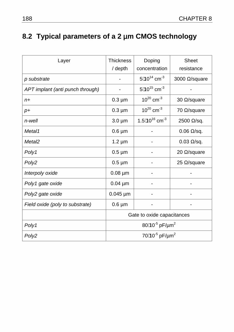
188 CHAPTER 8
8.2 Typical parameters of a 2 µµµµm CMOS technology
Layer Thickness
/ depth
Doping
concentration
Sheet
resistance
p substrate - 5⋅1014 cm-3 3000 Ω/square
APT implant (anti punch through) - 5⋅1015 cm-3 -
n+ 0.3 µm 1020 cm-3 30 Ω/square
p+ 0.3 µm 1020 cm-3 70 Ω/square
n-well 3.0 µm 1.5⋅1016 cm-3 2500 Ω/sq.
Metal1 0.6 µm - 0.06 Ω/sq.
Metal2 1.2 µm - 0.03 Ω/sq.
Poly1 0.5 µm - 20 Ω/square
Poly2 0.5 µm - 25 Ω/square
Interpoly oxide 0.08 µm - -
Poly1 gate oxide 0.04 µm - -
Poly2 gate oxide 0.045 µm - -
Field oxide (poly to substrate) 0.6 µm - -
Gate to oxide capacitances
Poly1 80⋅10-5 pF/µm2
Poly2 70⋅10-5 pF/µm2

APPENDIX 189
8.3 Conversion: LUMEN, WATT and CANDELA
Conversion of candela (cd) to watt (W)
[ ] [ ] [ ] ( )eve V
1sranglecdIW
λ⋅⋅=Φ
Iv Light intensity in candela
V(λe) Spectral luminous intensity. Normalized to the human spectral
daylight viewing sensitivity.
Φe Radiant flux in watt
Conversion of lumen (lm) to Watt (W)
[ ] [ ] ( )eve V
1lmW
λ⋅Φ=Φ
Φv Luminous flux in lumen
Φe Radiant flux in watt
V(λe) Spectral luminous intensity
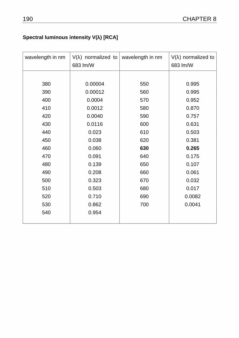
190 CHAPTER 8
Spectral luminous intensity V(λλλλ) [RCA]
wavelength in nm V(λ) normalized to
683 lm/W
wavelength in nm V(λ) normalized to
683 lm/W
380
0.00004
550
0.995
390 0.00012 560 0.995
400 0.0004 570 0.952
410 0.0012 580 0.870
420 0.0040 590 0.757
430 0.0116 600 0.631
440 0.023 610 0.503
450 0.038 620 0.381
460 0.060 630 0.265
470 0.091 640 0.175
480 0.139 650 0.107
490 0.208 660 0.061
500 0.323 670 0.032
510 0.503 680 0.017
520 0.710 690 0.0082
530 0.862 700 0.0041
540 0.954

APPENDIX 191
8.4 Measurement conditions (MCD) for Chapter 5
MCD01:
Sequencer (Justin’s sequencer + sequencer II) Quartz: 16 MHz clock division factor: 256 (CS0, CS1= 0, 1) sequencer clock: 62.5 kHz word period: 16 µs Camera setup Integration time: 50ms #clock cycles for integration time
3125 (3125*16µs=50ms)
measured points: 22 integration time increment: 2.4ms diffusing foil: folex film systems: folaproof Laserfilm/DM beidseitig matt, 90MY light source Schott KL1500 electronic (cold-light source) IF Filter: Coherent-Ealing, CWL: 633nm, HBW: 38nm, XT: 38% camera board: miniaturized board (Elantec drivers) lens: 4mm, 1:1.2, CS mount Data acquisition: 12 bit enhanced parallel port interface (CSEM product)
MCD02:
LED: 630nm HPWT-DH00 not pulsed, Illumination with microscope Power of LED: 6.7uW (total behind ocular and 630nm Filter) Diameter of light spot (on chip): 19mm (behind the filter) Area of light spot: 19mm*19mm*pi/4=284mm2 ! Power-density on chip: 23.6 fW/µm2 Size of photo gates: 144um2 ! Power on photogate: 3.4pW Integration time: 125ms ! Energy on PG: 425fJ Energy of 630nm photon: 3.16 E-19J ! Number of incoming photons: 1’340’000 (per pixel) QE at 630nm: 65% ! Number of integrated electrons: 900'000 (per pixel) Charge of integrated electrons: 1.44E-13C
! Calculated output voltage swing: 3.25 V Measured output voltage: 3.60 V

192 CHAPTER 8
MCD03S:
Conditions SCCD Illumination with microscope; LED pulsed at 1MHz (1:1 on/off ratio); 630nm IF-filter used; optical power measured behind the IF-filter IF-Filter (COHERENT-EALING 42-7344):
CWL: 633nm; HBW: 38nm; XT: 82%
LED: HPWT-DH00 LED average current 50mA Modulation frequency 1MHz Spot diameter: 22mm Total power of spot: 6.0µW, Spot area: 380⋅106µm2 Wavelength: 630nm Size of photogates: 144µm2 Integration time: 125ms per
Tap Power on photogate: 2300 fW
Energy of 630nm photon: 3.16 E-19J Energy on photogate: 288 fJ Quantum efficiency QE630nm: 65% #photons per photogate: 910’000 Conversion capacitance: 40fF #electrons integrated per pixel: 590’000 Amplification of SF stage: 0.9 charge of #electrons int. 95 E-15 C output voltage swing (measured) 2.3V output voltage swing (theory) 2.15V
Again, measured output voltage swing and theoretically calculated voltage swing are nearly the same.
MCD03B:
Conditions BCCD
Illumination with microscope; LED pulsed (average current: 50mA); 630nm IF-filter used; optical power measured behind the IF-filter IF-Filter (COHERENT-EALING 42-7344):
CWL: 633nm; HBW: 38nm; XT: 82%
LED: HPWT-DH00 Spot diameter: 17mm Total power of spot: 1.4µW, Spot area: 227⋅106µm2 Wavelength: 630nm Size of photogates: 144µm2 Integration time: 125ms per
Tap Power on photogate: 888 fW
MCD04S:
Conditions SCCD
LED 630nm (HPWT-DH00), 50mA average Amplitude C1 C2 Rise/fall time PGL, PGR: 8V 120pF 680pF 5ns IG 10.7V Integration time 125ms per Tap
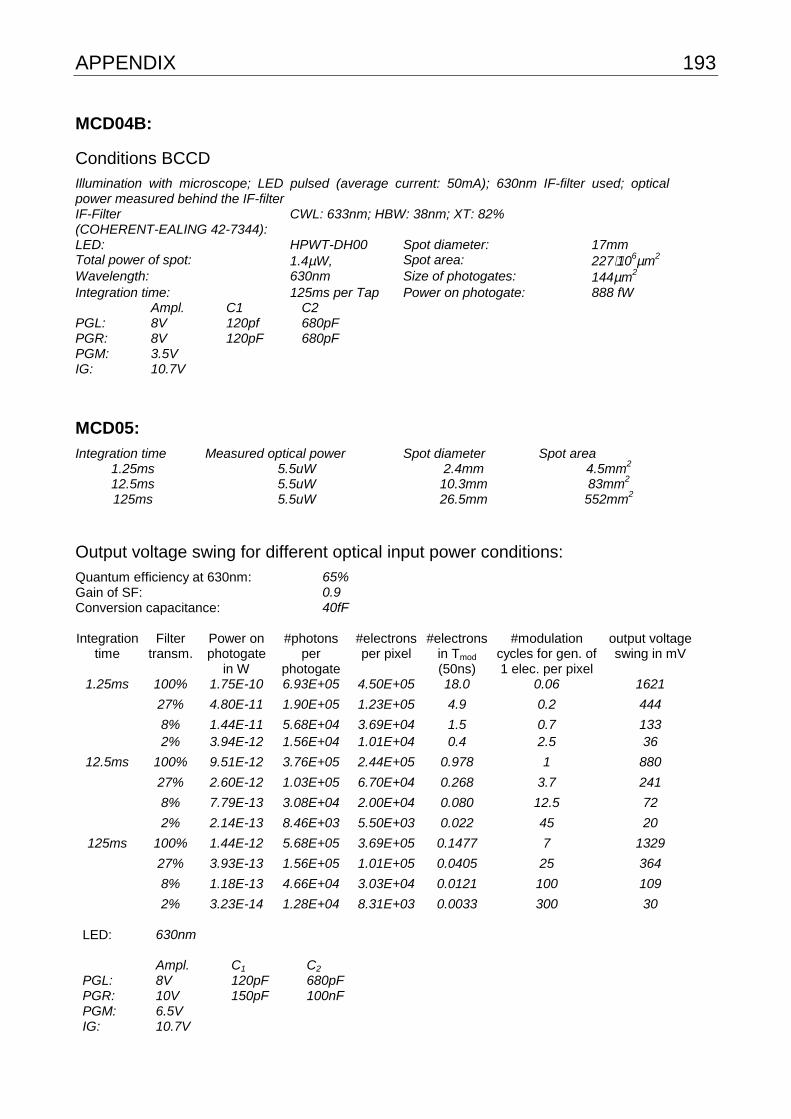
APPENDIX 193
MCD04B:
Conditions BCCD Illumination with microscope; LED pulsed (average current: 50mA); 630nm IF-filter used; optical power measured behind the IF-filter IF-Filter (COHERENT-EALING 42-7344):
CWL: 633nm; HBW: 38nm; XT: 82%
LED: HPWT-DH00 Spot diameter: 17mm Total power of spot: 1.4µW, Spot area: 227⋅106µm2 Wavelength: 630nm Size of photogates: 144µm2 Integration time: 125ms per Tap Power on photogate: 888 fW Ampl. C1 C2 PGL: 8V 120pf 680pF PGR: 8V 120pF 680pF PGM: 3.5V IG: 10.7V
MCD05:
Integration time Measured optical power Spot diameter Spot area 1.25ms 5.5uW 2.4mm 4.5mm2 12.5ms 5.5uW 10.3mm 83mm2 125ms 5.5uW 26.5mm 552mm2
Output voltage swing for different optical input power conditions:
Quantum efficiency at 630nm: 65% Gain of SF: 0.9 Conversion capacitance: 40fF
Integration
time Filter
transm. Power on photogate
in W
#photons per
photogate
#electrons per pixel
#electrons in Tmod (50ns)
#modulation cycles for gen. of 1 elec. per pixel
output voltage swing in mV
1.25ms 100% 1.75E-10 6.93E+05 4.50E+05 18.0 0.06 1621
27% 4.80E-11 1.90E+05 1.23E+05 4.9 0.2 444
8% 1.44E-11 5.68E+04 3.69E+04 1.5 0.7 133 2% 3.94E-12 1.56E+04 1.01E+04 0.4 2.5 36
12.5ms 100% 9.51E-12 3.76E+05 2.44E+05 0.978 1 880
27% 2.60E-12 1.03E+05 6.70E+04 0.268 3.7 241
8% 7.79E-13 3.08E+04 2.00E+04 0.080 12.5 72
2% 2.14E-13 8.46E+03 5.50E+03 0.022 45 20
125ms 100% 1.44E-12 5.68E+05 3.69E+05 0.1477 7 1329
27% 3.93E-13 1.56E+05 1.01E+05 0.0405 25 364
8% 1.18E-13 4.66E+04 3.03E+04 0.0121 100 109
2% 3.23E-14 1.28E+04 8.31E+03 0.0033 300 30
LED:
630nm
Ampl. C1 C2 PGL: 8V 120pF 680pF PGR: 10V 150pF 100nF PGM: 6.5V IG: 10.7V

194 CHAPTER 8
MCD06S:
Measurement conditions (SCCD)
Illumination with microscope; no IF-filter used; average LED current: 50mA LEDs: 4 different Spot diameter: 22mm Wavelengths: 470, 630, 740, 850nm Spot area: 380⋅106µm2 Integration time: 125ms per Tap Size of photogates: 144µm2 Total power of spot (meas. only for 630nm LED: HPWT-DH00):
5.1µW @ 1kHz 6.0µW @ 10kHz 6.0µW @ 100kHz 5.5µW @ 10MHz 4.3µW @ 20MHz
Power on pixel (630nm LED):
1930fW @ 1kHz 2270fW @ 10kHz 2270fW @ 100kHz 2080fW @ 10MHz 1630fW @ 20MHz
PGL 8V PGR 10V PGM 6.5V
MCD06B:
Measurement conditions (BCCD)
Illumination with microscope; no IF-filter used; average LED current: 50mA LEDs: 4 different Spot diameter: 17mm Wavelengths: 470, 630, 740, 850nm Spot area: 227⋅106µm2 Integration time: 125ms per Tap Size of photogates: 144µm2 Total power of spot (meas. only for 630nm LED: HPWT-DH00):
1.4µW @ 20MHz
Power on pixel (630nm LED):
888fW @ 20MHz
PGL 8V PGR 8V PGM 3.5V
MCD07:
Measurement conditions and distance accuracy achieved Number of average runs: (1) No AVG Control voltages: PGL PGM PGR 8V 3.5V 8V Standard deviation of error Average voltage swing: 72 mV in ns: 0.26 ns Optical power on the photogate: 736 fW in cm: 3.84 cm integration timer per Tap 12.5ms resulting frame rate 20Hz modulation frequency: 20MHz
REFERENCES 195
References
[AME] G. Amelio et al., “Experimental Verification of the Charge Coupled Device
Concept”, Bell Syst. Tech. Jour., Vol. 49, pp. 593-600, (1970).
[BEH] G. Beheim and K. Fritsch, “Range finding using frequency-modulated laser
diode”, Applied Optics, Vol. 25, pp. 1439-1442 (1986).
[BER] J. Beraldin et al., “Registered intensity and range imaging at 10 mega-
samples per second”, Optical engineering, Vol. 31, No. 1, pp. 88-94,
(1992).
[BES] P. Besl, “Active Optical Range Imaging Sensors”, Machine Vision and
Applications, Vol. 1, pp. 127- 152, (1988).
[BEY] J. Beynon, et al., “Charge-coupled devices and their applications”,
McGRAW-HILL Book Company, (1980).
[BIB] A. Biber, “Avalanche photodiode image sensing in standard silicon
BiCMOS technology”, Ph.D. Dissertation ETH Zurich, Switzerland, No.
13544, (2000).
[BLC] N. Blanc et al., “Digital low-power camera on a chip”, Proc. International
COST 254 Workshop on Intelligent Communication Technologies and
Applications, Neuchâtel, Switzerland, (1999).
[BLU] C. Blumer, “Characterization of a SCCD, a BCCD and a new Narrow-
channel-BCCD line”, Internship at CSEM Zurich, (1999).
[BOU] S. Bourquin, “Low-coherence interferometry based on customized detector
arrays”, Ph.D. Dissertation EPFL-Lausanne, Switzerland, No. 2171,
(2000).
[BOY] W. Boyle et al., “Charge coupled semiconductor devices”, Bell Syst. Tech.
Jour., Vol. 49, pp. 587-593, (1970).
[BRE] B. Breukmann, “Bildverarbeitung und optische Meßtechnik“, Franzis’,
(1993).
196
[BRK] Brockhaus, “Naturwissenschaften und Technik”, Bd. 3, ISBN 3-7653-0450-
6, Mannheim, (1989).
[BRR] H. Breuer, “dtv-Atlas zur Physik, Tafeln und Texte”, Bd.1, 2.Auflage, ISBN
3-423-03226-x, (1990).
[CAR] J.E. Carnes et al., “Free Charge Transfer in Charge-Coupled Devices”,
IEEE Transactions on Electron Devices, Vol. 19, No.6, (1972).
[COR] S. Coren et al., “Sensation and Perception”, Fourth Edition, Harcourt Brace
College Publishers (1994).
[CRE] K. Creath, “Phase-Measurement Interferometry Techniques”, Progress in
Optics, Vol. XXVI, E. Wolf (Ed.), Elsevier, (1988).
[CS1] CSEM Zurich, Badenerstrasse 569, CH-8048 Zurich.
[DAS] Product brochure of Daimler-Benz Aerospace, “Laserkamera”, contact:
[DEC] S. Decker et al., “A 256x256 CMOS imaging array with wide dynamic
range pixels and column-parallel output”, Proceedings of IEEE
International Solid-State Circuits Conference, (1998).
[DOR] R. G. Dorsch et al., “Laser triangulation: Fundamental uncertainty in
distance measurement”, Applied Optics, Vol. 33, pp. 1306-1314, (1994).
[ELA] Élantec Data Book, EL7202CS CCD driver, (1997).
[EMM] Product data sheet, “APSVGA- Low-power CMOS digital video camera”,
EM Marin, (1999).
[EN2] K. Engelhardt, “Meßprinzipien, Eigenschaften und Limitierungen. Optische
3D-Meßtechnik”, Technische Rundschau, Issue 31, pp. 44-51, (1993).
[ENG] K. Engelhardt, “Methoden und Systeme der optischen 3-D Messtechnik”,
XI. Internationaler Kurs für Ingenieurvermessung in Zürich, Ferd.
Dümmlers Verlag Bonn, (1992).
[FEM] http://www.femto.de
[FOS] E. Fossum, “Active Pixel Sensors: Are CCD’s Dinosaurs?”, Proceedings of
the SPIE, Vol. 1900, pp. 2-14, (1993).
REFERENCES 197
[FUR] M. Furumiya et al., “A ½-inch 1.3N-Pixel Progressive Scan CCD Image
Sensor Employing 0.25 mm Gap Single-Layer Poly-Si Electrodes",
Proceedings of IEEE International Solid-State Circuits Conference, San
Francisco, (1999).
[HAM] Hamamatsu prospectus, “Image Intensifiers”, (1994).
[HAU] F. Hauser, “Internship at CSEM Zurich”, CSEM-internal report, (2000).
[HEC] E. Hecht, A.Zajac, “OPTICS”, Addison-Wesley, (1974).
[HEK] P. Heck, “Operation and characterization of a surface channel CCD-line”,
Diploma work (Travail pratique de Diplôme), EPFL Lausanne/ CSEM
Zurich, (1999).
[HOF] B. Hoffmann, “Einsteins Ideen”, Spektrum Akademischer Verlag, 1997;
Translation of: “Relativity and Its Roots“, Scientific American Books, New
York, (1983).
[HOP] C. R. Hoople et al., “Characteristics of Submicrometer Gaps in Buried-
Channel CCD Structures”, IEEE Transactions on electron devices, Vol. 38,
No. 5, (1991).
[HOP] G. Hopkinson, et al. “Noise reduction techniques for CCD image sensors”,
J. Phys. E : Sci. Instrum., Vol. 15, pp. 1214-1222, (1982).
[HP1] Hewlett Packard (now Agilent), “Super Flux LEDs, Technical Data”, Data
sheet of HP SunPower Series, including HPWT-DH00, (1998).
[HP2] Hewlett Packard (now Agilent), “Super Flux LED, Categories and Labels”,
Application Note 1149-7, (1998).
[JE1] G. Jellison et al. “Optical functions of silicon at elevated temperatures”,
Journal of Applied Physics, 76, (1994).
[JE2] G. Jellison, “Optical functions of silicon determined by two-channel
polarization modulation ellipsometry”, North-Holland Physics Publishing,
Optical Materials 1, pp. 41-47, (1992).
[KA2] H. A. Kappner, “Verfahren und Anordnung zur dreidimensionalen
optischen Erfassung von Objekten”, European Patent No. 0 192 993 A1,
(1986).
198
[KAI] I. Kaisto, et al., “Optical range finder for 1.5m - 10m distances”, Applied
Optics, Vol. 22, No. 20, 3258-3264, (1983).
[KAP] H. Kappner, „Dreidimensionale sensorische Erfassung von Werkstücken“,
documentation of OPSIS GmbH, Speyer, Germany, (1987).
[KOE] W. Koechner, “Optical Ranging System Employing a High Power Injection
Laser Diode”, IEEE Transactions on Aerospace and Electronic Systems,
Vol. AES-4(1), pp. 81-91, (1968).
[KRA] J. Kramer, “Photo-ASICs: Integrated Optical Metrology Systems with
Industrial CMOS Technology”, Ph.D. Dissertation ETH Zurich, Switzerland,
No. 10186, (1993).
[LA1] R. Lange et al., “Time-of-flight range imaging with a custom solid-state
image sensor”, Proceedings of the SPIE, Vol. 3823, pp. 180-191, Munich,
(1999).
[LA2] R. Lange, et al, “Demodulation pixels in CCD and CMOS technologies for
time-of-flight ranging”, Proceedings of the SPIE, Vol. 3965A, pp. 177-188,
San Jose, (2000).
[LA3] R. Lange, et al., “Seeing distances - A fast time-of-flight 3D camera”,
Sensor Review, Vol. 20, Issue 3, July 2000, to be published, (2000).
[LAX] S. Lauxtermann et al., “A high speed CMOS imager acquiring 5000
frames/sec”, IEEE: IEDM Technical Digest, pp. 875-878, Washington DC,
(1999).
[LEI] http://www.leica.com/surv-sys/index.asp.
[MAZ] “Echtzeit-3D-Board zur Tiefenauswertung stereoskopischer Bilder”,
Prospectus of MAZ Mikroelektronik Anwendungszentrum Hamburg GmbH,
(1999).
[MOI] A. Moini, “Vision Chips or Seeing Silicon”, 3rd Rev., Department of
Electronics Engineering, The University of Adelaide, Australia, (1997).
[MOR] I. Moring et al., “Acquisition of three-dimensional image data by a scanning
laser rangefinder”, Optical Engineering, Vol. 28, pp. 897-905, (1989).
[PAR] J. Parker et al., “Reflective tomography: images from range-resolved laser
radar measurements”, Applied Optics, Vol. 27, pp. 2642-2643, (1988).
REFERENCES 199
[PHS] “Laser-Radar Imaging without Scanners”, Photonics Spectra, April 1994,
pp. 28-30, (1994).
[POW] H. Powel et al., ”Charge-coupled device image sensors as a demodulator
in a 2D-polarimeter with a piezoelastic modulator”, Applied Optics, Vol. 29,
No 8, pp. 1186-1190, (1990).
[PS1] P. Seitz, “Solid-State Image Sensing”, in Handbook of Computer Vision
and Applications, B. Jähne, H. Haussecker and P. Geissler (Eds.),
Academic Press, (1999).
[PS2] P. Seitz, “Image sensing with maximum sensitivity using industrial CMOS
technology”, Proceedings of the SPIE, Vol. 3099, Munich, (1997).
[RCA] RCA, “Electro-Optics Handbook”, Technical Series EOH-11, Commercial
Engineering, Harrison, NJ 07029, (1974).
[RIG] Internet: http://www.riegl.co.at, (1998).
[RIX] M. Rioux, “Laser range finder based on synchronized scanners”, Applied
Optics, Vol. 23, No 21, pp. 3837-3844, (1984).
[SAL] B. Saleh, M. Teich, “Fundamentals of Photonics”, ISBN 0-471-83965-5,
John Wiley & Sons, (1991).
[SC1] R. Schwarte, “Principles of 3-D Imaging Techniques”, in Handbook of
Computer Vision and Applications, B. Jähne, H. Haussecker and P.
Geissler (Eds.), Academic Press, (1999).
[SC2] R. Schwarte et al., “Pseudo- noise (PN)- laserradar without scanner for
extremely fast 3D-imaging and navigation”, MIOP ’97, Stuttgart, (1997).
[SC3] R. Schwarte et al., “A new active 3D-Vision system based on rf-modulation
interferometry of incoherent light”, Photonics East-Intelligent Systems and
Advanced Manufacturing, Proceedings of the SPIE, Vol. 2588,
Philadelphia, (1995).
[SEQ] C. Séquin, et al., “Charge Transfer Devices“, Academic Press, (1975).
[SLO] J. Szydlo, et al., “Air-turbine driven optical low-coherence reflectometry at
28.6 kHz scan repetition rate”, Optics communications, 154, pp. 1-4,
(1998).
200
[SP1] T. Spirig et al., “The lock-in CCD – Two-dimensional synchronous
detection of light”, IEEE Journal of quantum electronics, Vol. 31, No. 9, pp.
1705-1708, (1995).
[SP2] T. Spirig et al., “The multitap lock-in CCD with offset subtraction”, IEEE
Transactions on electron devices, Vol. 44, No. 10, pp. 1643-1647, (1997).
[SP3] T. Spirig, P. Seitz, “Vorrichtung und Verfahren zur Detektion und
Demodulation eines intensitätsmodulierten Strahlungsfeldes”, German
Patent No. DE 44 40 613 C 1, (1996).
[SP4] T. Spirig, “Smart CCD/CMOS Based Image Sensors with Programmable,
Real-time, Temporal and Spatial Convolution Capabilities for Applications
in Machine Vision and Optical Metrology”, Ph.D. Dissertation ETH Zurich,
Switzerland, No. 11993, (1997).
[STR] T. Strand, “Optical three-dimensional sensing for machine vision”, SPIE’s
Optical Engineering, Vol. 24 (1), pp. 33-40, (1985).
[SUT] D. Sutter et al., “self-starting 6.5fs pulses from a Ti:sapphire laser using a
semiconductor saturable absorber and double-chirped mirrors”, IEEE
Journal of Selected Topics in Quantum Electronics , Vol. 4, pp. 169-178,
(1998).
[SZ1] S. Sze, “Semiconductor Devices, Physics and Technology”, 1st edition,
John Wiley & Sons, (1985).
[SZ2] S. Sze, “Physics of semiconductor devices”, 2nd edition, John Wiley &
Sons, (1981).
[TEU] A. Theuwissen, “Solid-State Imaging with Charge-Coupled Devices“,
Kluwer Academic Publishers, (1995).
[TIE] U. Tietze, C. Schenk, “Halbleiter- Schaltungstechnik”, 10th edition,
Springer-Verlag, (1993).
[TOR] J. R. A. Torrea et al., “Matching photometric-stereo images”, J. Opt. Soc.
Am. A, Vol. 15, pp. 2966-2975, (1998).
[VIZ] O. Vietze, “Active pixel image sensors with application specific
performance based on standard silicon CMOS processes”, Ph.D.
Dissertation ETH Zurich, Switzerland, No. 12038, (1997).
REFERENCES 201
[VOG] T. Vogelsong et al., “Scientific/industrial camera-on-a-chip using Active
Column Sensor TM CMOS technology”, Proceedings of the SPIE, Vol.
3965A, San Jose CA, (2000).
[WON] H. Wong, “Technology and device scaling considerations for CMOS
imagers“, IEEE Transactions on Electron Devices, Vol. 43, No. 12, (1996).
[XU] Z. Xu, “Investigation of 3D-Imaging Systems Based on Modulated Light
and Optical RF-Interferometry (ORFI) - ZESS-Forschungsberichte”, Shaker
Verlag Aachen, ISBN 3-8265-6736-6, (1999).
[ZIM] E. Zimmermann et al., “Stabilized three-wavelength source calibrated by
electronic means for high-accuracy absolute distance measurements”,
Optics Letters, Vol. 21, pp. 531-533, (1996).


ACKNOWLEDGMENTS 203
Acknowledgments
This work has been carried out in the Image Sensing Group of the PSI (Paul
Scherrer Institut), which later became part of CSEM (Centre Suisse d’Electronique
et de Microtechnique SA) in Zurich, Switzerland. I would like to thank the section
head of this group, Prof. Peter Seitz for his supervision and guidance of this work
during the last three years. He gave many fruitful inputs for this work and my
publications. Especially he taught me how to be efficient in my work.
Also I would like to thank Prof. Rudolf Schwarte for agreeing to be my Ph.D. advisor
and for leading me into the world of Photonics.
Furthermore, I must not forget to thank Dr. Alice Biber for introducing me to CMOS
IC design and for her permanent practical and mental support of my work. We had
many interesting discussions about technical problems and other things in life. She
always knew the right questions to ask. Additionally, Alice reviewed nearly every
English sentence I produced during my work.
I owe thanks to my officemate Dr. Nicolas Blanc, who always had an open ear to
my problems and provided me with coffee and other fruitful inputs.
I gratefully acknowledge the invaluable help of Peter Metzler in all kinds of analog
electronic problems. For digital electronics and CCD drivers I could profit from the
profound experience of Dr. Peter Schwider. For assisting me in “C” programming
and English language problems, and for discussing the latest sports events I thank
Graham Lang.

204
I thank my friends Thomas Ammer, Dr. Gerd Blau, Vincenzo Monterosso (thanks
for extending my horizons at the rock concert in Hallenstadion), Dr. Stephane
Bourquin and Philipp Zeller for their social and technical support.
It is a pleasure to express my thanks also to all other members of the Image
Sensing Group, who contributed to this work in one way or the other: Dr. Kai
Engelhardt, Dr. Stefan Lauxtermann, Dr. Roger Dangel, Martin Wäny, Georg Israel,
Dr. Michel Willemin, Gerben Boer and not to forget Ernst Meier.
I do not want to forget to thank my family, who were always interested in my work
and my life. My parents, who made possible my complete education, and my
brother Christoph and my sister Kathrin, who also were always there for me, when I
needed them. Most important of all, my thanks go to my wife Anja for her love,
support and patience over the last years.
In case I should have forgotten anyone, I beg for generous forgiveness.
The work was partly funded by the Swiss Priority Program OPTIQUE II, whom we
thank for this support.
206
Publication list
1. R. Lange, P. Seitz, “Solid-state time-of-flight range camera”, IEEE Journal of
Quantum Electronics, submitted for publication, (2000).
2. R. Lange, P. Seitz, “Seeing distances - A fast time-of-flight 3D camera”, Sensor Review, Vol. 20, No. 3, July 2000, pp. 212-217, MCB University Press, ISSN
0260-2288, (2000).
3. R. Lange, P. Seitz, “Demodulation pixels in CCD and CMOS technologies for time-of-flight ranging”, Proceedings of the SPIE, Vol. 3965A, pp. 177-188, San
Jose CA, (2000).
4. R. Lange, P. Seitz, “Real-time range camera based on a novel imager with demodulation pixels”, SPIE’s International Technical Group Newsletter, Vol. 10,
No. 2, Bellingham, (1999).
5. R. Lange, P. Seitz, R. Schwarte, “Time-of-flight Entfernungskamera in
CMOS/CCD- Technik mit pixelintegrierten optischen Lock-in-Verstärkern”, Berichtsband 70 zur Fachtagung Optische Formerfassung 1999, pp. 271-280,
VDI-VDE, Stuttgart, (1999).
6. R. Lange, P. Seitz, A. Biber, R. Schwarte, “Time-of-flight range imaging with a custom solid-state image sensor”, Proceedings of the SPIE, Vol. 3823, pp. 180-
191, Munich, (1999).
7. R. Lange, P. Seitz, “Solid-State Time-of-Flight Distance Measurement System
Based on Novel Lock-in Sensors”, Proceeding of IWOM99, The International
Workshop on Optical Metrology (CD), Liverpool John Moores University, School
of Engineering, (2000).
8. H. Heinol, R. Schwarte, Z. Xu, H. Neuhaus, R. Lange, “First Experimental results
of a New 3D-Vision System Based on RF-Modulation Interferometry”,
Kongreßband OPTO96- Optische Sensorik Meßtechnik Elektronik, AMA
Fachverband für Sensorik, pp. 67-72, Leipzig, (1996).
9. Z. Xu, R. Schwarte, H. Heinol, R. Lange, J. Li, “Simulation of a 3D-color vision
system based on synthetic non-linear modulation”, Proceedings of the SPIE, Vol. 2904, pp. 361-369, Boston MA, (1996).
Patent pending
R. Lange, P. Seitz, “Device and method for spatially resolved photodetection
and demodulation of modulated electromagnetic waves”, (2000).