CMOS ACTIVE PIXEL SENSOR -...
81
CMOS ACTIVE PIXEL SENSOR BY NITIN N. VELUDANDI Master’s Technical Report Electrical Engineering New Mexico State University Las Cruces, New Mexico August 2006 Advisor: Paul M Furth
Transcript of CMOS ACTIVE PIXEL SENSOR -...

CMOS ACTIVE PIXEL SENSOR
BY
NITIN N. VELUDANDI
Master’s Technical Report
Electrical Engineering
New Mexico State University
Las Cruces, New Mexico
August 2006
Advisor: Paul M Furth

i
“CMOS Active Pixel Sensor,” a master technical report prepared by Nitin N Veludandi,
in partial fulfillment of the requirement for the degree, Master of Science in Electrical
Engineering, has been approved and accepted by the following:
Linda Lacey Dean of the Graduate School
Paul M. Furth Chair of the Examining committee Date
Committee in charge:
Dr. Paul M. Furth, Chair
Dr. Steve Stochaj
Dr. Jeffrey Beasely

ii
Dedicated to ma, dad, nikki, neellakka,.nishananna, kittubawa peddamma and
peddananna

iii
ACKNOWLEDGEMENTS
I want to thank and pay my regards to my advisor Dr. Paul M. Furth for his
guidance and for giving me the opportunity to work under him.
I would also like to thank Dr. Steve Stochaj for helping me to understand the DE2
board and concepts of VHDL. I am also grateful for his help during building of the test
setup.
I also want to thank Dr. Jeff Beasely for agreeing to be on my defense committee.
I wish to thank Dr. Jaime Ramirez-Angulo for his guidance in the VLSI field and
for helping me to understand the basic concepts of VLSI design.
I also want to thank Sreeker Reddy, Vamsy P.Ponnapureddy and Aditya
Rayankula for helping me during my thesis.

iv
VITA
May 29, 1982 Born in Hyderabad, A.P, India
May 2004 Bachelor of Technology (B.Tech.) in Electronics and Computer Engineering from Jawaharlal Technological University,
India August 2005-May 2006 Graduate Research Assistant, Department of WERC, New Mexico State University August 2005-May 2006 Graduate Teaching Assistant, Department of ECE, New Mexico State University
Field of Study
Major Field: Electrical Engineering (VLSI )

v
ABSTRACT
CMOS ACTIVE PIXEL SENSOR
BY
NITIN NARESH VELUDANDI
Master of Science in Electrical Engineering
New Mexico State University
Las Cruces, New Mexico, 2006
Dr. Paul M. Furth, Chair
The aim of this project is to build a chip that will detect the light incident on it and
convert the image into analog voltages. This is implemented using a 32 x 32 array of
pixels, each pixel consisting of a photodiode (photo sensor) and circuitry to read the data
from the photodiode.
The Active Pixel Sensor designed uses a concept called Correlated Double
Sampling to reduce the pixel fixed-pattern noise. The difference between the reset value
and the integrated photo value is called the correlated double sample. The difference is
computed outside the chip.
The voltage values (reset and photo) are read out using digital circuitry. A 5 x 32
decoder is used to select a single row at a time and a 32 x 1 multiplexer is used to select a
single column at a time. The input select lines to the multiplexer and decoder are the
outputs from a 12-bit counter. The counter runs at a 2MHz clock frequency.

vi
The outputs of the chip are the analog sample voltages coming out at a 2 MHz
sampling frequency. These voltages are converted to digital voltages and are analyzed to
regenerate the image incident on the sensor.
A data acquisition system has been developed to test the sensor. The system
consists of a high-speed A/D converter running at 30Msps with 3.3Vpower supply. This
data is collected by the Altera DE2 board. The DE2 board includes an FPGA chip and an
SRAM cell. The FPGA is programmed using VHDL to store the data in SRAM. The data
from the SRAM is transferred to the host computer via a USB port using software
provided by the manufacturer, called the DE2 Control Panel.

vii
Index 1 INTRODUCTION ..................................................................................................................................... 1
1.1 PHOTO SENSOR ..................................................................................................................................... 1
1.2 IMAGE SENSOR ..................................................................................................................................... 1
2. BACKGROUND ....................................................................................................................................... 4 2.1 CCD IMAGE SENSORS .......................................................................................................................... 4
2.2 CMOS IMAGE SENSORS ....................................................................................................................... 4
2.2.1 Passive Pixel Sensor .................................................................................................................... 5 2.2.2 Active Pixel Sensor ...................................................................................................................... 6
2.3 IMAGE SENSOR RESOLUTION ................................................................................................................ 6
2.4 IMAGE SENSOR ASPECT RATIO ............................................................................................................. 7
2.5 FRAME RATE ........................................................................................................................................ 7
2.6 COLOR FIDELITY .................................................................................................................................. 7
2.7 CMOS IMAGE SENSOR NOISE .............................................................................................................. 8
2.7.1 Fixed Pattern (Spatial) Noise....................................................................................................... 8 2.7.2 Temporal Noise ............................................................................................................................ 9 2.7.2.1 Pixel Noise ................................................................................................................................ 9 2.7.2.2 Column Amplifier Noise .......................................................................................................... 10 2.7.2.3 Programmable Gain Amplifier Noise ..................................................................................... 11 2.7.2.4 ADC Noise .............................................................................................................................. 12 2.7.2.5 Dynamic Range ....................................................................................................................... 12
2.8. CMOS IMAGE SENSOR ARCHITECTURE ............................................................................................. 12
2.8.1 3T Architecture .......................................................................................................................... 13 2.8.2 4T/5T Architecture ..................................................................................................................... 14
3 DESIGN AND SIMULATIONS ............................................................................................................. 16 3.1 ACTIVE PIXEL SENSOR ....................................................................................................................... 16
3.2 PHOTO PIXEL ...................................................................................................................................... 18
3.3 COLUMN CIRCUIT ............................................................................................................................... 21
3.4 DECODER 5 X 32 ................................................................................................................................. 24
3.5 32 X 1 MULTIPLEXER .......................................................................................................................... 28
3.5.1 4 x 1 Multiplexer ........................................................................................................................ 30 3.6 12-BIT COUNTER ................................................................................................................................ 31
3.6.1 Half Adder .................................................................................................................................. 34 3.6.2 THE D-FLIP FLOP ............................................................................................................................. 36
3.7 THE VARIABLE INTEGRATION (VI) LOGIC .......................................................................................... 38

viii
4 TEST SETUP AND PROCEDURE ....................................................................................................... 41 4.1 CHIP DESCRIPTION: ............................................................................................................................ 41
4.2 CHIP DESCRIPTION ............................................................................................................................. 41
4.3 TEST PROCEDURE ............................................................................................................................... 45
4.3.1 Test Procedure of Digital Circuits: ............................................................................................ 45 4.3.2 Test procedure of a single pixel: ................................................................................................ 46 4.3.3 Test Procedure of the column circuit: ........................................................................................ 47
4.4 DATA ACQUISITION SYSTEM SETUP: .................................................................................................. 48
4.4.1 A/D Setup ................................................................................................................................... 48 4.4.2 Prototype Board Setup ............................................................................................................... 50 4.4.3 DE2 Setup: ................................................................................................................................. 50 4.4.4Test Procedure for VHDL Code: ................................................................................................ 51 4.4.5 Test Procedure for MATLAB Code: ........................................................................................... 52
4.5 TEST PROCEDURE FOR THE ACTIVE PIXEL SENSOR ............................................................................ 53
5 TEST RESULTS AND CONCLUSIONS .............................................................................................. 56 5.1 TEST RESULTS OF TEST PHOTO PIXEL ................................................................................................ 56
5.2 TEST RESULTS FOR THE COLUMN CIRCUIT. ........................................................................................ 57
5.3 TEST RESULTS OF DIGITAL CIRCUITS ................................................................................................. 58
5.4 TEST RESULTS OF ACTIVE PIXEL SENSOR ........................................................................................... 60
THE DARK LINE WHICH APPEARS ON THE 31ST COLUMNS SHOWS THAT THERE IS A COLUMN FAIL. THE
COLUMN FAIL IS NOT DUE CIRCUIT, ITS DUE TO THE RETRIEVAL OF THE DIGITAL DATA FROM THE SRAM IN
THE DE2 BOARD. THE WHITE SPOTS IN IMAGE INDICATE THAT THE PIXELS HAVE REACHED TO
SATURATION. IN FUTURE MORE CONSTANT LIGHT SOURCED SHOULD BE USED TO HAVE A UNIFORM IMAGE.
A CONCAVE LENS SHOULD BE USED TO FOCUS THE IMAGE ON THE SENSOR IN ORDER TO GET MORE
ACCURATELY DISTINGUISHABLE IMAGE. .................................................................................................. 62
5.5 CONCLUSIONS AND FUTURE WORK .................................................................................................... 63
REFERENCES ........................................................................................................................................... 65 APPENDIX A: ............................................................................................................................................ 66 APPENDIX B: ............................................................................................................................................ 68

ix
LIST OF TABLES Table Page 3.1 Modes of Sensor Operation 30
3.2 Truth Table for 5 x 32 Decoder 39
3.3 Truth Table for 5-input NAND Gate 40
3.4 Truth Table for 4 x 1 Multiplexer 43
3.5 Truth Table for XOR Gate 47
3.6 Truth Tale for 2-input AND Gate 47
3.7 Truth Table of Reset and Tx Signal for Different Integration Times 50
4.3 Pin Table .................................................................................................... 54

x
LIST OF FIGURES
Figure Page
2.1 CCD Image Sensor Block Diagram 15
2.2 CMOS Image Sensor Block Diagram 16
2.3 3T Architecture 26
2.4 4T/5T Architecture 28
3.1 Block Diagram of Active Pixel Sensor 30
3.2 Simulation Model of Photodiode 32
3.3 Schematic of Photodiode 33
3.4 Simulation Results of Photo Pixel 34
3.5 Column Circuit 35
3.6 Schematic of Voltage Follower 36
3.7 AC Response of the Differential Amplifier 37
3.8 Transient Response of Voltage follower 38
3.9 Block Diagram of Decoder and Each Cell Schematic 39
3.10 Schematic of 5-input NAND Gate 41
3.11 Simulation Results of 5 x 32 Decoder for bits D0-D7 42
3.12 Block Diagram of 32 x 1 Multiplexer 43
3.13 Schematic of 4 x 1 Multiplexer 44
3.14 Simulation Results of 4 x 1 Multiplexer 45
3.15 Block Diagram of 12-bit Counter 46
3.16 Single Cell of Counter 46
3.17 Schematic of a Half Adder Circuit 47
3.18 Simulation Results of 2-input XOR Gate 48

xi
3.19 Simulation Results of 2-input AND Gate 48
3.20 Schematic of D-Flip Flop 49
3.21 Simulation Results of D-Flip Flop 50
3.22 Simulation Results of 12-bit Counter 50
3.23 Boolean Expressions 51
3.24 Simulation Results of VI Logic Block 52
4.1 Pin Configuration of APS with Test Structures 54
4.2 Testing Single Pixel 57
4.3 Pin Configuration of Test Pixel 58
4.4 Testing Voltage Follower 59
4.5 Pin Configuration of Test Column Circuit 59
4.6 Testing Digital Circuits 60
4.7 Pin Configuration of Digital Circuits 61
4.8 Testing Active Pixel Sensor 62
4.9 Pin Configuration of Active Pixel Sensor 64
4.10 Test Setup of A/D Converter 65
4.11 Pin Configuration of A/D Converter 69
5.1 Test Results of Single Pixel 70
5.2 MATLAB plot of Single Pixel using 32 x 32 Array 70
5.3 Test Results of Column Circuit 71
5.4Test Results of Reset Signal at 1024μs 71
5.5 Test Results of Tx signal 71
5.6 Test Results of row Signal 72

xii
5.7 MATLAB Plot of Active Pixel Sensor 73
5.8 MATLAB Plot of Active Pixel Sensor 73
5.9 MATLAB Plot of Active Pixel Sensor 74
5.10 MATLAB Plot of Active Pixel Sensor 74

1
1 INTRODUCTION
1.1 Photo Sensor A photo sensor is a transducer which converts light energy to electrical energy.
That means a photo sensor converts the photons incident on it to electron flow (current).
A photo sensor is made up of semiconductor material, generally silicon, that has a
property called photoconductivity. The generation of electrons in an electric field
depends on the intensity of light incident on it [WHATI].
The photodiode, bipolar phototransistor, and photo FET (photosensitive field-
effect transistor) are the three most commonly used photo sensors. The working of these
devices is the same as a regular diode, bipolar transistor and field effect-transistor,
respectively. The difference between a photo sensor and an ordinary device (MOS, BJT)
is that photo sensors have light as an input. These device have transparent windows that
allow light energy to fall on it [WHATI]. The photo sensor used in this project is the
photodiode.
1.2 Image Sensor A device which converts the visual scene to electrical signals is called an image
sensor. The main application of image sensors is the digital camera. An image sensor
consist of an array of pixels which are characterized by either CCD technology or CMOS
technology. Before the existence of CMOS image sensors, CCD cameras were dominant.
CCD’s were mainly used in astronomical telescopes, scanners and video camcorders.
After CMOS sensors came into existence, CCD reduced in importance, due to the low
cost and the ability to integrate different functions in CMOS sensors. CMOS image

2
sensors have eventually become the image sensor of choice in a large segment of the
market. Both CCD and CMOS image sensors capture light on a grid of small pixels on
their surfaces. However the processing of the signal and how they are manufactured
distinguishes them. [WIKIP]
There are several major types of color image sensors, differing by the means of
the color separation:
The Bayer Sensor: The most common and low-cost sensor is the Bayer filter, which
passes red, green, or blue light to selected pixels, forming a fixed pattern grid sensitive to
red, green, and blue. The values of these color filters are interpolated using a demosaicing
algorithm [WIKIP].
The Foveon X3 Sensor: An array of layered sensors is used, where every pixel contains
three overlapped phototransducers, each sensitive to the individual colors [WIKIP].
The 3CCD Sensor: Three discrete image sensors are used, where the color separation is
done by a dichroic prism. This sensor is considered to be the best in terms of quality, and
is more expensive than single-CCD sensors [WIKIP].
The sensor used in this project does not have any color filter array on the pixels.
Only black and white images are captured. In general the active pixel sensor designed in
this project can only capture the black and monochromatic images.

3
In this technical report, we outline the design, simulation, and testing of a CMOS
active pixel image sensor. Chapter 2 gives the basic background of various types of
sensors and their working. Chapter 3 describes the design and simulations of each block
of the CMOS Active Pixel Sensor. Chapter 4 gives the test setup and test procedure of the
CMOS APS. Chapter 5 has the conclusions and tests results of the sensor.

4
2. BACKGROUND
2.1 CCD Image Sensors CCD Image Sensors were invented in 1969 by Bell Laboratories. At the time,
digital photography was the major field of application. Upon exposure of the sensor, the
charge on the first row (row of pixels) is transferred to the read out register. The read out
register signals are fed to an amplifier and then on to an analog-to-digital converter. Once
the row has been read, the charges on the readout register row are deleted, the next row is
transferred to the first row and this procedure is carried on till last row is read
out[SHORT].
2.2 CMOS Image Sensors Unlike CCD’s CMOS image sensors are manufactured in factories called fabs.
The basic difference between CCD’s and CMOS is that in CMOS Image sensors there are
circuits which help us to store and read out the photo value whenever needed. CMOS is
the highest yielding chip-making process in the world. The latest CMOS processors, such
as the Pentium IV, contain almost 55 million active elements. As a result of these
Fig 2.1 CCD Imager Block Diagram [SHORT].
5
economies of scale, the cost of fabricating a CMOS wafer is one-third the cost of
fabricating a similar wafer using a specialized CCD process. Costs are lowered even
farther because CMOS image sensors integrate the pixel along with circuitry, unlike
CCDs, which requires processing circuits on a separate chip. Early versions of CMOS
image sensors had lots of noise problems, and were used mainly in low-cost cameras.
However, later versions of the CMOS sensors have relatively low noise and have quality
equal to CCD’s [SHORT].
There are two basic kinds of CMOS image sensors—passive and active.
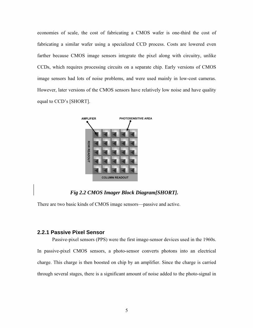
2.2.1 Passive Pixel Sensor Passive-pixel sensors (PPS) were the first image-sensor devices used in the 1960s.
In passive-pixel CMOS sensors, a photo-sensor converts photons into an electrical
charge. This charge is then boosted on chip by an amplifier. Since the charge is carried
through several stages, there is a significant amount of noise added to the photo-signal in
Fig 2.2 CMOS Imager Block Diagram[SHORT].
6
this process. To cancel out this noise, additional processing steps are required,
sometimes on chip and sometimes off chip. [SHORT].
2.2.2 Active Pixel Sensor Active-pixel sensors (APSs) reduce the noise associated with passive-pixel
sensors. Each pixel has an extra circuit, an amplifier, which helps cancels the noise
associated with the pixel. It is from this concept that the active-pixel sensor gets its name.
The performance of this technology is similar to charge-coupled devices (CCDs) and also
allows for a larger image array and higher resolution [SHORT]. The Image sensor used in
this project to capture an image is an Active Pixel Sensor.
2.3 Image Sensor Resolution Image resolution is a measurement of how sharp images are. The most
professional digital cameras have a total 12-million pixels (3000 x 4000). The human eye
has 120 million pixels and 35mm film has 20 million pixels. These values are difficult to
match by a CMOS imager, but the technology is getting closer to those numbers
[SHORT].
A description of the screen display (that is, the number of pixels on a screen)
introduced the term “resolution" in the computer world. For example, a screen may have
1024 pixels horizontally and 768 pixels vertically. The resolution of the active pixel
sensor in this project is 32 x 32. However, to photographers, and for the optical
community, resolution is the ability of a device to resolve lines such as those found on a
test chart [SHORT].

7
2.4 Image Sensor Aspect Ratio The ratio of image height to image width defines the aspect ratio. This ratio is
always represented in the form W:H where W is the width and H is the height. Most
image sensors fall in between the equality ratio (1:1) and the 35mm film ratio (1.5:1).
The aspect ratio of a sensor determines the shape and proportions of the image taken.
Images of different aspect ratio can be resized by a concept called cropping. Cropping is
a code generated (for example, in MATLAB) to resize the images to the required aspect
ratio. Sometimes we may loose data or clarity by cropping [SHORT]. The aspect ratio
used in this project is 1:1 (32 rows and 32 columns).
2.5 Frame Rate
Frame rate is the rate at which an entire image is taken, meaning, how fast the
image is first acquired by the sensor and then read out. The frame rate can also be defined
as the inverse of the number of images taken in one second. The term is mostly used in
video cameras, computer graphics and in motion capture systems [SHORT]. The frame
rate is most often expressed in frames per second (fps) or simply, Hertz (Hz). This project
has a frame rate of 976.5 Hz.
2.6 Color Fidelity The ability to replicate colors of an image in a real scene by a sensor is called
color fidelity. In an imaging world, it is essential to maintain the flexibility to allow color
to be graded for the desired image quality. Color digital imaging is a complicated process
due to the fact that electronic imagers are monochromatic. The difference between red
photons and blue photons is distinguished by silicon through color filters on each of the
pixels. These color filters pass only specific wavelengths of light based on the filter used.

8
Post processing after readout is done to replicate the intensity of the color incident on that
particular pixel. Different approaches all have different impacts on sensitivity, resolving
power, and the design of the overall system [SHORT]. There are no filters used in this
project, so the output image is just a core image that differentiates intensities at each
pixel.
2.7 CMOS Image Sensor Noise CMOS image sensors have poor image quality compared to CCD sensors due to
high fixed pattern noise (FPN), high dark current and poor sensitivity. Finding out the
noise sources and canceling the noise will improve the image quality in CMOS
technology. Noise sources are present from the sensor photodiode through the column
and programmable gain amplifiers (PGA) and analog-to-digital converters (ADC) in each
and every part of the sensor [NOISE].
2.7.1 Fixed Pattern (Spatial) Noise FPN refers to spatial noise and is due to device mismatches in the pixels,
variations in the column amplifiers and mismatches between multiple PGAs and ADCs.
Dark current FPN, due to mismatches in the pixel photodiode leakage currents,
tends to dominate, especially with long exposure times. Low leakage photodiodes reduce
this FPN component. Dark frame subtraction is another option to reduce the dark current
FPN component but it increases the readout time of the sensor [NOISE].
The most common FPN in image sensors is associated with rows and columns
due to mismatches in multiple signal paths, and un-correlated, row operations in the

9
image sensor. Most of this error results in offset, or dc, noise, which can be canceled
using a technique called correlated double-sampling. On the other hand, gain mismatches
are more difficult to remove, since they require more sample time for gain correction
[NOISE].
2.7.2 Temporal Noise Temporal noise is the time-dependent fluctuations of the signal level, unlike FPN
which is fixed. Temporal noise can be found in the pixel, column amplifiers,
programmable gain amplifiers and ADCs. There is also circuit-oriented temporal noise
due to substrate coupling or poor power supply rejection [NOISE].
2.7.2.1 Pixel Noise Noise sources in the pixel are the photon shot noise, reset (kT/C) noise, dark
current shot noise and the MOS device noise [NOISE].
Pixel Photon Shot Noise
Photon absorption is a random process following Poisson statistics. This means
that the standard deviation (or noise) of the photon noise limits the Signal-to-Noise Ratio
(SNR) associated with detecting a mean of N photons. The SNR is equal to the square
root of the number of photons absorbed and is given by [NOISE]:
NSNR =)photon( (2.1)
Photon shot noise limits the SNR when the detected signals are large. The system
noise floor determines the lower limit of the dynamic range of the sensor. The difference
between the largest and smallest signal detected is called the dynamic range [NOISE].
10
Pixel Reset (kT/C) Noise
The signal integrated on a pixel is measured relative to its reset level. The thermal
noise associated with this reset level is called the reset or the kT/C noise. The correlated-
double-sampling technique is used to eliminate the majority of this noise [NOISE].
Pixel Dark Current Shot Noise
Pixel Shot Noise is due to the photodiode leakage current, Idark, and is dependent
on the exposure time τ given by:
qIC
qdark
pix
/Voltsin Noise τ= (2.2)
Where Cpix is the total pixel capacitance and q is the electronic charge [NOISE].
MOS Device Noise
The amplifier noise in the pixels is due to the thermal and flicker (1/f) noise of the
MOS transistors. 1/f noise can be eliminated through double sampling of a single pixel.
Thermal noise in the MOS devices can be reduced by limiting the bandwidth of the pixel
amplifier (a source follower) using a large capacitive load [NOISE].
2.7.2.2 Column Amplifier Noise The column circuit stores both the pixel reset and photo sample values, and
amplifies the difference signal. Major noise sources that are associated with this circuit
are the kT/C thermal noise and flicker noise [NOISE].
Column Amplifier kT/C Noise
11
The two sampling operations associated with the signal and reset levels result in a
thermal noise signal given by:
Noise = 2kTC(Column)
(2.3)
Ccolumn is the column sampling capacitance; k is Boltzmannn’s constant; and T is the
absolute temperature in degrees Kelvin. A further 3dB increase in column kT/C noise can
be done if dark reference columns are used to reduce column fixed-pattern noise
[NOISE].
Column Amplifier MOS Device Noise
Flicker noise present in the column amplifier MOS devices is negligible
compared to the sampling operation kT/C noise [NOISE].
2.7.2.3 Programmable Gain Amplifier Noise Noise sources in the programmable gain amplifiers are the kT/C thermal noise
related to the sampling operations and the programmable gain MOS device noise
[NOISE].
Programmable Gain MOS device Noise
MOS amplifier thermal and flicker noise is much smaller than the sampling
operation kT/C noise [NOISE]. Lower noise is generally achieved by using larger-area
devices and operating at higher bias current levels.
Programmable Gain kT/C Noise
12
In the column amplifier case, two sampling operations are performed, and the
associated thermal noise signal is given by [NOISE]:
Noise = 2kTC(pga)
(2.4)
2.7.2.4 ADC Noise The biggest noise source in a high-performance ADC is the quantization noise.
An ideal ADC’s quantization noise is given by:
Noise = LSB12
(Volts) (2.5)
= 0.288 x LSB (Volts)
The ADC noise level will exceed 0.288LSB due to other noise sources like thermal,
amplifier and switching noise. Random mismatches in the ADC components also
contribute to fixed-pattern noise in the ADC [NOISE].
2.7.2.5 Dynamic Range The ratio of the largest signal to the smallest simultaneous signal (noise floor) is
defined as the dynamic range of a CMOS sensor [NOISE], It is generally expressed in
dB.
2.8. CMOS Image Sensor Architecture Passive CMOS sensor pixels (one transistor per pixel) had a good fill factor but
suffered from very poor signal to noise performance. Active CMOS sensors came into
existence to reduce the noise in passive sensors. Most of the CMOS designs today use
active pixel sensors, which have an amplifier in each pixel, a source follower typically
13
constructed with three transistors. A pixel with three transistors is known as the 3T pixel.
Other CMOS pixel designs include more transistors (4T and 5T) for specific reasons to
reduce noise and/or to achieve simultaneous shuttering. The simpler structures have
better fill factor and higher density while the more complex structures have more
functionality. Functionality versus density is one major tradeoff [NOISE].
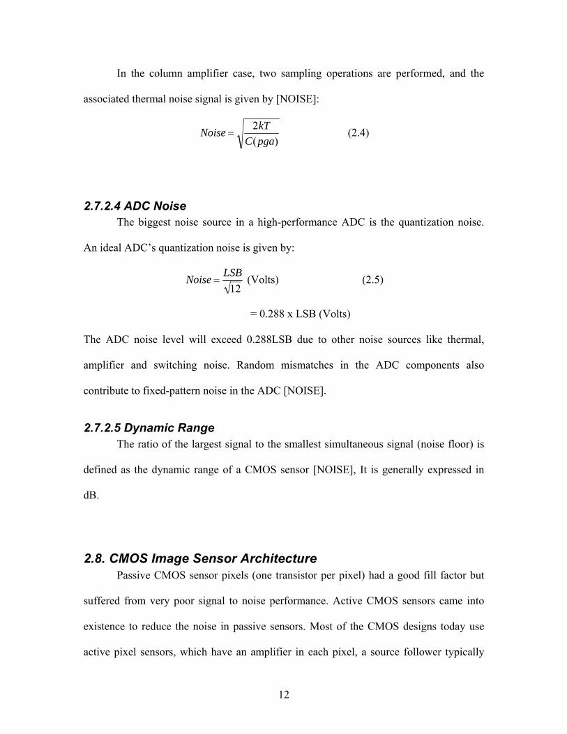
2.8.1 3T Architecture Fig 2.3 shows the 3T architecture APS. The three transistors are the reset
transistor, source follower and the row select transistor. When reset is higher, the pixel is
in reset mode. When reset is low, the pixel integrates at a rate dependent on the light
falling on it. The source follower transistor is used to transfer the voltage from the photo-
diode to the column line through a row select transistor.

14
2.8.2 4T/5T Architecture Fig 2.4 shows the 4T/5T architecture. The architecture is similar to 3T
architecture except it has one tranfer gate and a MOScap. The transfer gate is used to
program the integration time in order to have a good quality image. The MOScap is used
to prevent the loss of data from the pixel and to reduce kT/C noise. The use of a transfer
gate avoids the use of a rolling shutter, as is commonly used in the 3T architecture. The
total array acts as an analog memory, storing each pixel values in the cell.
Fig 2.4 4T/5T Architecturevss
vdd
RstTx
vdd
row
Photo Diode
Mrst
Mtx
Msf
Msel
Mcap
Column
Line
Fig 2.3 3T Architecture

15
In this project, the 4T/5T architecture is used for each pixel
16
3 DESIGN AND SIMULATIONS
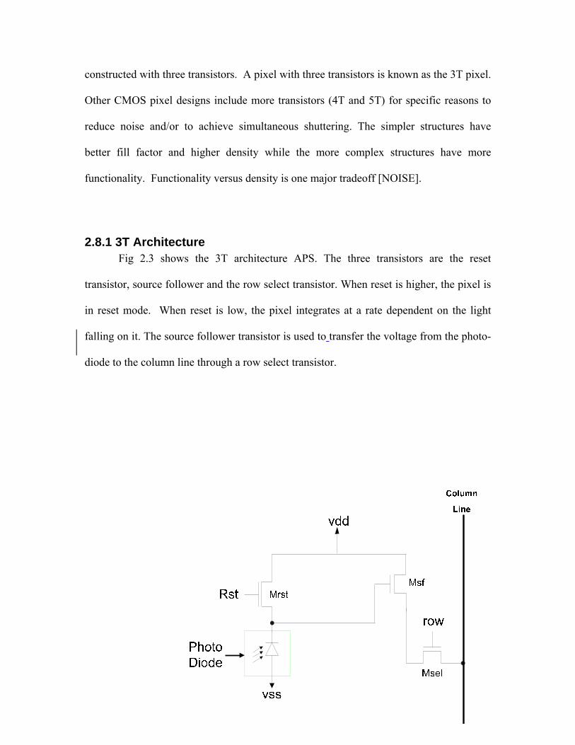
3.1 Active Pixel Sensor The active pixel sensor uses the principle of taking two samples from the same
pixel and then subtracting it in order to reduce fixed-pattern noise and to get a better
quality image. This principle is known as correlated double sampling. The circuitry
which controls the reading out of a pixel’s voltage is mostly digital. Fig 3.1 shows the
block diagram of an active pixel sensor design.
The active pixel sensor design in this project consists of a 32x32 array of pixels.
The light incident on this array is stored on a MOSFET capacitor (MOScap) in the pixel
and then is read out using the decoder and multiplexer. A 12-bit counter is used to
generate the signals for the multiplexer and the decoder. The decoder selects one row at a
time. When a row is selected, the sampled value in each row is fed to the column. There
32X1 Multiplexer
32
32
32X1 Decoder
32x1 Columns
32X32 pixels
Vout12-Bit Counter
Q0-Q4
Q5-Q9
VI Logic
Q10,Q11
4X1 Multiplexer
3
Fig 3.1 Block Diagram of Active Pixel Sensor

17
are 32 column circuits, one for each column in the pixel array. The value stored in the
column is then read out using the 32x1 multiplexer. In order to vary the integration time,
a Variable Integration (VI) logic block is used. The VI logic block generates three
different reset pulses with three different integration times: 256μs, 512μs, and 1024μs,
respectively. These integration times are selected using a 4:1 multiplexer. The sensor
works at a frequency of 2 MHz, allowing 0.5μs of time between two successive samples.
The voltage generated by the light incident on the pixels is read out first, followed by the
reset value.
There are three modes of operation: integration mode, sample mode, and reset
mode. Integration mode is when integration of the photo-current takes place. Sample and
reset modes are when the reset and sample values are read out. The table below shows the
2 MSB’s (Q10 and Q11) of the counter and the corresponding modes.
The rows and columns are selected only during the sample and reset modes, so
that we read only relevant data. In order to accomplish this task, the decoder and
multiplexer select signals are passed through two-input AND gates where the other input
is the Q11 bit of the counter. This allows the sensor to select rows and columns only in
sample and reset mode. (Refer to table 3.1.)
Q11 Q10 Mode 0 0 Integration0 1 Integration1 0 Sample 1 1 Reset
Table 3.1 Modes of Sensor operation
18
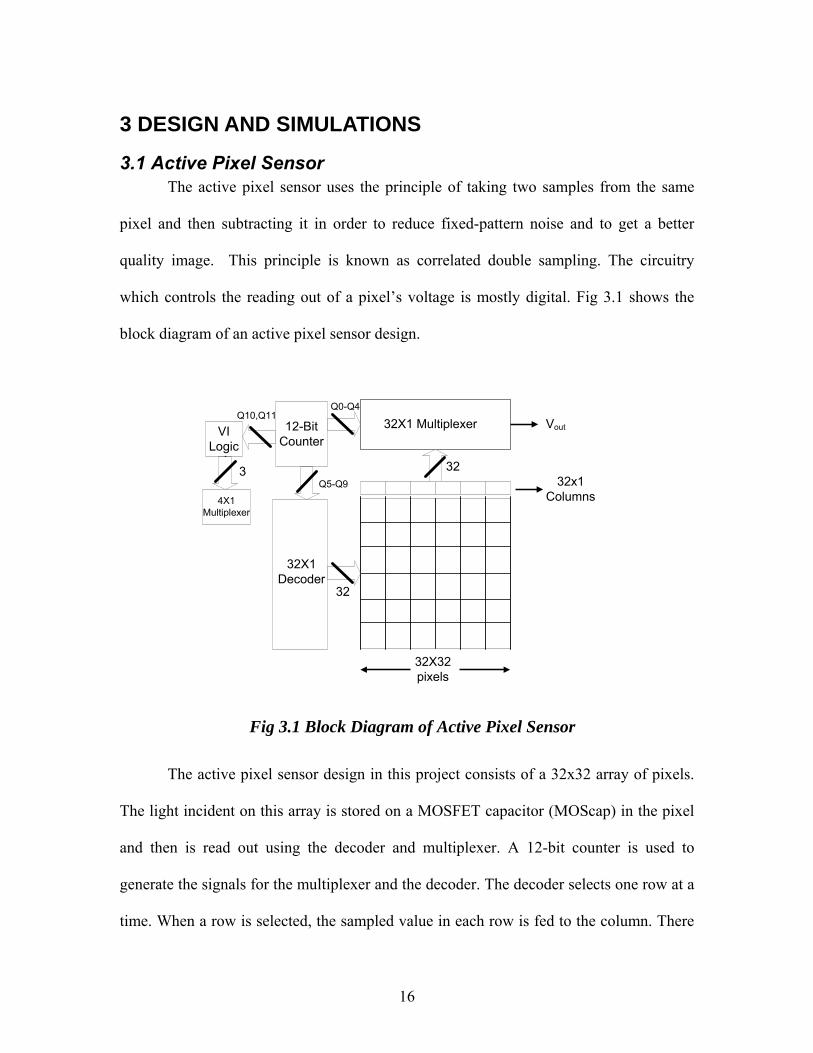
3.2 Photo Pixel A photo pixel consists of a photodiode, a few control transistors, a MOS
amplifier, and a MOScap to capture the light intensity. The photo pixel used in this
project is the 4T/5T architecture. It consists of 4 transistors, a MOScap and a photodiode.
The basic premise behind the photodiode front end is to indirectly measure the
relatively small photocurrent by converting it into a large voltage swing. We also require
the circuit which performs this current-to-voltage conversion to occupy a small amount of
area on the chip.
The photodiode senses the light falling on it and a photocurrent flows through it.
The photocurrent is converted into a voltage using a load. The photodiode is modeled as a
parasitic capacitance in parallel with a current source. The photodiode with a load and the
equivalent circuit model is shown in figure 3.2
Fig 3.2 Simulation Model of Photo Diode.

19
Fig 3.3 shows the 4T/5T pixel architecture used in this project. The photodiode is
pulled up towards Vdd through an NMOS transistor load, Mrst, whose gate is connected to
the reset signal. The value sampled is actually stored on the MOScap, whose gate is
connected to Vdd. The TX signal controls the value to be stored using an NMOS pass gate,
Mtx. The voltage on the MOScap is buffered through a source follower amplifier, Msf.
The pixel output value is transferred to the column line using a row signal through Msel.
When reset is high, the value at node Vpix is Vdd -Vthn, since there is a threshold
drop at the reset transistor. The signal TX stays high for the desired integration time
(256μs, 512μs or 1024μs) and goes low only in sample mode. The value measured on the
column line at the output of the source follower is Vdd -2 Vthn since there is a second
Fig 3.3 Schematic of a Photo Pixel.
20
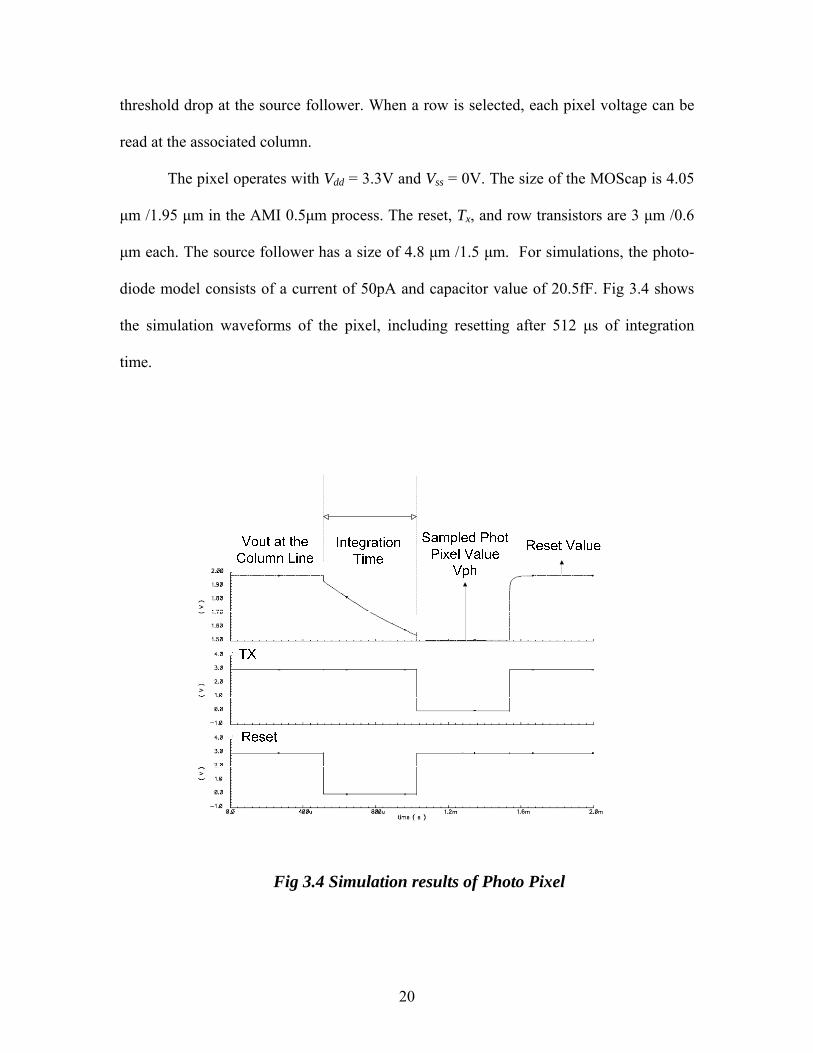
threshold drop at the source follower. When a row is selected, each pixel voltage can be
read at the associated column.
The pixel operates with Vdd = 3.3V and Vss = 0V. The size of the MOScap is 4.05
μm /1.95 μm in the AMI 0.5μm process. The reset, Tx, and row transistors are 3 μm /0.6
μm each. The source follower has a size of 4.8 μm /1.5 μm. For simulations, the photo-
diode model consists of a current of 50pA and capacitor value of 20.5fF. Fig 3.4 shows
the simulation waveforms of the pixel, including resetting after 512 μs of integration
time.
Fig 3.4 Simulation results of Photo Pixel

21
Vout is the sampled value. It integrates when reset is low and holds when TX is low.
The sudden glitch in the sampled value when reset goes low is due to charge injection
from the NMOS pass transistor when it turns off. The sampled value again resets itself
when reset and TX signals are high.
3.3 Column Circuit The column circuit consists of a current mirror, a PMOS capacitor, and a PMOS-
input voltage follower. The current mirror draws a current of 10μA for dynamically
discharging the value at the capacitor in order to store the next row’s value. Fig 3.5
shows the column circuit. The output from the pixel is given to the column line. An
external resistor of 230kΩ generates a current of 11μA.
Fig 3.5 Column Circuit.

22
An external resistor of 90kΩ generates a current of 33μA to bias the voltage
follower. The circuit works with Vdd = 3.3V and Vss = 0V. Fig 3.6 shows the schematic of
the amplifier used in the voltage follower. The amplifier has an open-loop gain of 35.1
dB, or 57 V/V, and a bandwidth of 1 MHz.
Fig 3.6 Schematic of voltage follower.
Vinm
vdd
vss
Vinp
34 μA DC
5.401.80
2*(5.40) (1.80)
4*(5.40) (1.80)
4*(5.40) (1.80)
4*(5.40) (1.80)
Vout

23
Fig 3.7 shows the open loop AC response of the differential amplifier shown
in Fig. 3.6. The open loop gain is 35.1 dB, which corresponds to 57 Volts/Volts. The
cutoff frequency of the amplifier is 1MHz, so the gain-bandwidth (GBW) product is
57MHz. The voltage follower configuration of the differential amplifier has unity gain.
Since GBW is constant for a given amplifier, the cutoff frequency of the voltage follower
is 57MHz. The samples of the active pixel sensor come out at a 2MHz clock frequency.
The voltage follower cutoff frequency is way beyond 2MHz; hence, it is suitable for this
APS application.
Fig 3.7 AC Response of the Operational Amplifier.

24
Fig 3.8 shows the transient response of the voltage follower configuration. The
voltage follower configuration is where the negative input of the differential amplifier is
connected to the output and the input is given to the positive output. Vin is the input and
Vout is the output of the voltage follower. Vdd = 3V and Vss = 0V. Vin is a xxkHz sinusoid
with an amplitude of yyV. From the waveforms, we see that the output is the same as the
input. Hence, the voltage follower configuration of the differential amplifier is working
well.
3.4 Decoder 5 x 32 A 5 x 32 decoder is used to select each row in the array. There are 32 rows.
The input to the decoder is given from the counter outputs Q5-Q9. The decoder used here
Fig 3.8 Transient Response of the Amplifier.

25
is a simple NAND gate followed by 3 inverters for driving the row in the array. Fig 3.9
shows the block diagram of decoder.
There are 32 cells in a decoder, one for each row. Each cell is independent of
each other, except for the inputs. Each cell consists of a 5-input NAND gate with three
inverters. The circuit works at Vdd = 3V and Vss = 0V. A particular combination of inputs
selects only one cell in the decoder, meaning, the output of that cell is set to logic high.
All of the other cells are unselected, or logic low. The combination of inputs that select a
particular output is shown in Table 3.2.
Fig 3.9 Block Diagram of Decoder and each cell schematic.
D0
vddvdd vdd vdd
D1
vddvdd vdd vdd
vssvss
vss vss
D31
vddvdd vdd vdd
vssvss
vss vss
abcde
a b c d e

26
S4 S3 S2 S1 S0 output
selected 0 0 0 0 0 Row1 0 0 0 0 1 Row2 0 0 0 1 0 Row3 0 0 0 1 1 Row4 0 0 1 0 0 Row5 0 0 1 0 1 Row6 0 0 1 1 0 Row7 0 0 1 1 1 Row8 0 1 0 0 0 Row9 0 1 0 0 1 Row10 0 1 0 1 0 Row11 0 1 0 1 1 Row12 0 1 1 0 0 Row13 0 1 1 0 1 Row14 0 1 1 1 0 Row15 0 1 1 1 1 Row16 1 0 0 0 0 Row17 1 0 0 0 1 Row18 1 0 0 1 0 Row19 1 0 0 1 1 Row20 1 0 1 0 0 Row21 1 0 1 0 1 Row22 1 0 1 1 0 Row23 1 0 1 1 1 Row24 1 1 0 0 0 Row25 1 1 0 0 1 Row26 1 1 0 1 0 Row27 1 1 0 1 1 Row28 1 1 1 0 0 row29 1 1 1 0 1 Row30 1 1 1 1 0 row31 1 1 1 1 1 row32
Table 3.2 Truth Table for the Decoder

27
The right column in the Table 3.2 shows the row number which has been selected for a
particular input combination. The schematic of the 5-input NAND gate is shown in Fig
3.10 and the truth table for NAND in Table 3.3.
Fig 3.10 Schematic of 5-Input NAND Gate.
Table 3.3 Truth Table for NAND Gate
e d c b a Z 0 0 0 0 0 1 0 0 0 0 1 1 1 0 0 1 0 1 0 0 0 1 1 1 0 0 1 0 0 1 0 0 1 0 1 1 0 0 1 1 0 1 0 0 1 1 1 1 0 1 0 0 0 1 0 1 0 0 1 1 0 1 0 1 0 1 0 1 0 1 1 1 0 1 1 0 0 1 0 1 1 0 1 1 0 1 1 1 0 1
28
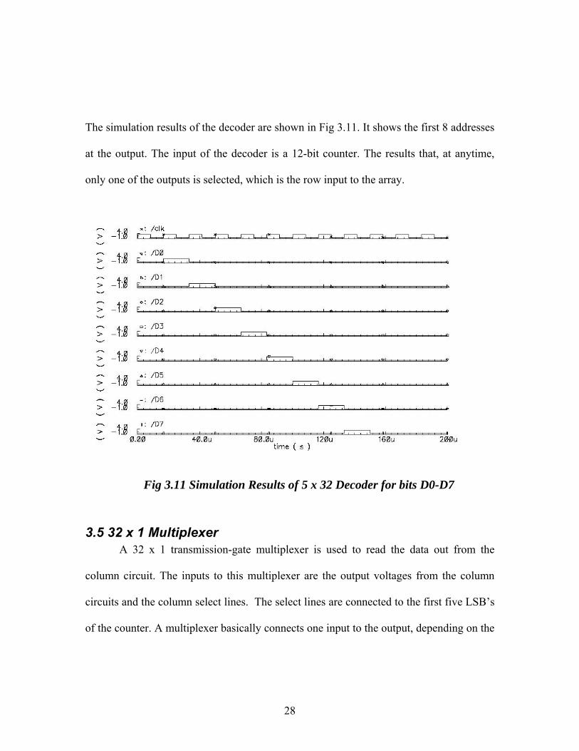
The simulation results of the decoder are shown in Fig 3.11. It shows the first 8 addresses
at the output. The input of the decoder is a 12-bit counter. The results that, at anytime,
only one of the outputs is selected, which is the row input to the array.
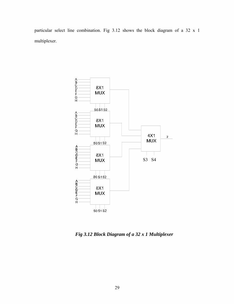
3.5 32 x 1 Multiplexer A 32 x 1 transmission-gate multiplexer is used to read the data out from the
column circuit. The inputs to this multiplexer are the output voltages from the column
circuits and the column select lines. The select lines are connected to the first five LSB’s
of the counter. A multiplexer basically connects one input to the output, depending on the
Fig 3.11 Simulation Results of 5 x 32 Decoder for bits D0-D7
29
particular select line combination. Fig 3.12 shows the block diagram of a 32 x 1
multiplexer.
Fig 3.12 Block Diagram of a 32 x 1 Multiplexer
S3 S4

30
3.5.1 4 x 1 Multiplexer A 4 x 1 multiplexer is used in selecting the different integration times for different
light intensities. Multiplexers in this project are designed using transmission gates. The
32 x 1 multiplexer must use transmission gates because it has to select one analog voltage
value from the column lines. Fig 3.13 shows the schematic of the multiplexer.
Fig 3.13 Schematic of 4 x 1 Multiplexer
S1 S0 Z 0 0 A 0 1 B 1 0 C 1 1 D
Table 3.4 Truth Table for 4 x1 Multiplexer

31
Table 3.3 shows the truth table for the 4 x 1 multiplexer for different
combinations of select lines. Simulation results for the 4 x 1 multiplexer are shown in Fig
3.14. The inputs A = Vdd, B = Vss, C = Vdd and D = Vss are given to the multiplexer. From
the waveforms we note that input S0 has twice the frequency of S1. When S0 and S1 are
logic ‘0’ the output is logic ‘1’ and when they are logic ‘1’ they are logic ‘0’. In a similar
way, they function correctly for the other combinations. This shows that the 4 x 1
multiplexer is working according to the specifications.
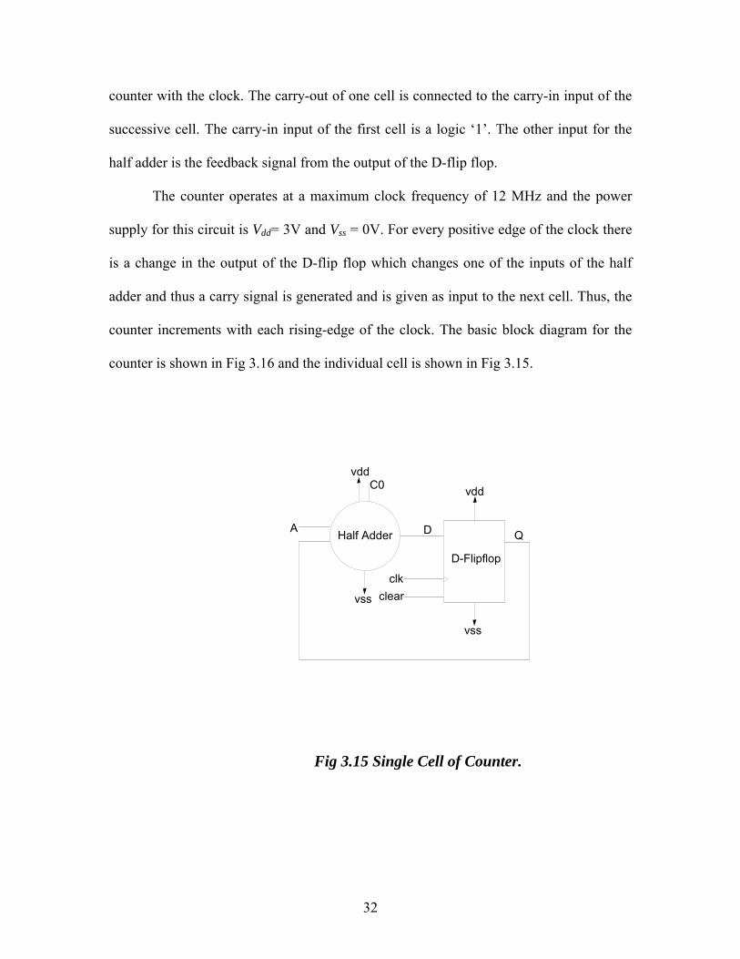
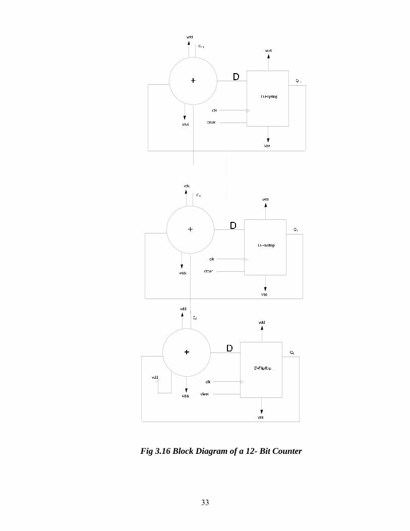
3.6 12-bit Counter A 12-bit ripple counter is used to select the rows and columns, and to program the
variable integration time logic in the active pixel sensor project. Each bit in the counter is
generated by a half adder and a D-flip flop. The D-flip flop is used to synchronize the
Fig 3.14 Simulation Results of 4X1 Multiplexer.
32
counter with the clock. The carry-out of one cell is connected to the carry-in input of the
successive cell. The carry-in input of the first cell is a logic ‘1’. The other input for the
half adder is the feedback signal from the output of the D-flip flop.
The counter operates at a maximum clock frequency of 12 MHz and the power
supply for this circuit is Vdd= 3V and Vss = 0V. For every positive edge of the clock there
is a change in the output of the D-flip flop which changes one of the inputs of the half
adder and thus a carry signal is generated and is given as input to the next cell. Thus, the
counter increments with each rising-edge of the clock. The basic block diagram for the
counter is shown in Fig 3.16 and the individual cell is shown in Fig 3.15.
Half Adder
vdd
vss
A
C0 vdd
vss
clkclear
D Q
D-Flipflop
Fig 3.15 Single Cell of Counter.
33
Fig 3.16 Block Diagram of a 12- Bit Counter

34
Fig 3.15 shows the schematic of each cell in the counter which is responsible for
producing one bit. Q is the output of one cell in the counter. Input A is the carry-in signal,
whereas output CO is the carry-out signal. Input A for the first cell is connected to Vdd
and for the other cells it is connected to the carry-out of the previous cell. Counting
occurs for every positive edge of the clock. In this project, the counter operates at a clock
frequency of 2 MHz.
3.6.1 Half Adder The half adder circuit has an XOR gate and an AND gate. The XOR gate
generates the sum bit and the AND gate gives the carry bit. Fig 3.17 shows the schematic
of the half adder.
Fig 3.17 Schematic of Half Adder Circuit.

35
The XOR gate is implemented using transmission gates in order to save power.
The AND gate is implemented using a NAND and an inverter. Table 3.4 and 3.5 shows
the truth tables of the XOR and AND gates, respectively.
Simulation results for XOR and AND gate are shown in Figs 3.21 and 3.22, respectively.
The AND and the XOR are important circuits in the counter, even though they are basic
elements. The AND generates the carry bit and the XOR the sum bit The AND and XOR
gates work according to the specifications
A B Z 0 0 0 0 1 1 1 0 1 1 1 0
Table 3.5 Truth Table of XOR Gate
A B Z 0 0 0 0 1 0 1 0 0 1 1 1
Table 3.6 Truth Table of AND Gate
Fig 3.18 Simulation Results of 2 Input XOR

36
3.6.2 The D-Flip Flop The D-flip flop is used to synchronize the counter with the clock. At every
positive clock edge the output follows the input and remains in that state till the next
positive clock edge. Thus, there is a change in the output at every positive clock edge.
The Clear signal is used to clear the output, that is, to set the output to logic 0 whenever
the clear signal is high. Fig 3.20 shows the schematic of the D-flip flop.
Fig 3.21 shows the simulation results of the D-flip flop. When clear is logic ‘1’
the output of the circuit is logic ‘0’. The circuit produces an output only when clear is
logic ‘0’. The output follows the input at every positive clock edge and holds the value
until the next clock event.
Fig 3.19 Simulation Results of 2 Input AND Gate

37
Fig 3.23 through fig 3.25 shows the simulation results of the up counter.
Fig 3.20 Schematic of the D-Flip Flop.
Fig 3.21 Simulation Results of D-Flip

38
Fig 3.22 shows the simulation results of first four LSB’s of the counter. Q0 is at
half the clock frequency, Q1 is at one-fourth the clock frequency Q2 is at one-eighth and
Q3 is at one-sixteenth the clock frequency. All the other bits work in same way,
decreasing in frequency by a factor of two from the previous bit.
3.7 The Variable Integration (VI) Logic The VI Logic is used to select the integration time. The three different times used
are 256μs, 512μs, and 1024μs. In order to generate these integration times, the last 3 bits
of the counter Q9, Q10, Q11 are used to generate R256 and the last 2 bits, that is, Q10 and
Q11, are used to generate R512 and R1024. The truth table for the reset and TX signals are
given in Table 3.6
Fig 3.22 Simulation Results of Up Counter for Bits

39
Q11 Q10 Q9 R256 0 0 0 1 0 0 1 1 0 1 0 1 0 1 1 0 1 0 0 1 1 0 1 1 1 1 0 1 1 1 1 1
Q11 Q10 R512 R1024 Tx 0 0 1 0 1 0 1 0 0 1 1 0 1 1 0 1 1 1 1 1
Table 3.7 Truth Table of Reset and TX Signals for different Integration Times.
Fig 3.24 Simulation Results of VI Logic Block
Fig 3.23 Boolean Expressions

40
Fig 3.23 shows the Boolean equations for the TX and different integration time’s
logic. Fig 3.24 shows the simulation results for the equations. The reset signals at 512μs
and 1024μs integration times operate correctly, but the reset at a 256μs integration time
does not work. The simulation results show that the R256 value becomes logic ‘0’ after Tx
becomes logic ‘1’. This circuit should be corrected in future work.

41
4 Test Setup and Procedure This chapter describes the test procedure for the CMOS active-pixel sensor.
4.1 Chip Description: The chip contains an image sensor used for optics applications along with
individual test circuits. It is a 40pin DIP prototype with 30 input/output pads. The chip
was submitted on March 27th, 2006.
4.2 Chip Description Analog Circuits Digital Circuits
Active Pixel Sensor with a 32 x 32 pixel
array.
12 bit Counter.
32 x 1 Analog Multiplexer. Variable Integration logic.
32 x 1 Column circuit. Decoder/Multiplexer logic.
5 x 32 Decoder.
4 x 1 Multiplexer.
The APS consist of 3 analog parts and 5 digital parts. The digital parts are
necessary for reading out the data from the pixel. The pixel and the voltage follower in
the column circuit forms the core analog parts. The area of the digital circuits in layout is
less than the analog circuitry since the pixel array occupies the major area in the layout.

42
Ib2
Ib1
Vout (TP)
vss (TP)
vdd (TP)
Vout(AB)
Avss (TC)
Vout(TC)
Vin(AB)
Avdd (TC)
pad_vdd
S0
S1
Q11
clk
clear
Dvdd
Dvss
pad_vss
Avdd (TS)
Avss (TS)
Vin(TS)
Vout (TS)
Ib1(TS)
Ib2(TS)
Vin (DB)
Vout (DB)
Vout (Rst)
Vout (Tx)
Vout (Row)
TP = Test Pixel.AB = Analog Buffer.TC = Total Chip.TS = Test Column Structure.DB = Digital Buffer.
Fig. 4.1 Pin configuration of the Active Pixel Sensor chip with test structures.

43
Pin Table:
Pin
Num
Pin
Name
Pad
Type
Pin
Type
Description
1 Ib2 Protect Input Biasing current for the voltage follower 2 KΩ
to VSS.
2 Ib1 Protect Biasing current for the column Circuit 7.5
KΩ to VDD.
4 Vout (TP) Protect Output Output voltage of single pixel.
5 Avss (TP) Protect 0V for the Test Pixel.
6 Avdd (TP) Protect Input 3.3V for test squaring circuit.
8 Vout (AB) Analog
Buffer
Output Output voltage of analog buffer test
structure.
9 Avss (TC) Protect Input 0V for the total chip (analog parts).
10 Vout (TC) Analog
Buffer
Output Analog Output of the total chip.
11 Vin (AB) Protect Input Input voltage of analog buffer test structure.
12 Avdd (TC) Protect Intput 3.3V for the total chip (analog parts).
16 Pad_vdd Vdd Input 3.3V for the pad frame.
17 S0 protect Input LSB of the multiplexer for Integration time
logic.
18 S1 Protect Input MSB of the multiplexer for Integration time
logic.
19 Q11 Protect Input MSB of the up-counter.
20 Clk Protect Input 2M Hz clock input to the chip.
21 Clear Protect Input Signal for clearing all digital buffers.
23 Dvdd Protect Input 3.3V to the digital circuits
24 Dvss Protect Input 0V to the digital circuits.

44
Pin
Num
Pin
Name
Pad
Type
Pin
Type
Description
25 pad_vss vss Input 0V to the pas frame.
30 AVdd (TS) Protect Input 3.3V to the column test circuit.
31 AVss (TS) Protect Input 0V to the column test circuit.
32 Vin (TS) Protect Input Input voltage for the column test circuit.
33 Vout (TS) Protect Output Output voltage of the column test circuit.
34 Ib1 (TS) Protect Input Biasing current for the column test circuit
230K Ω to vdd.
35 Ib2 Protect Input Biasing current for the voltage follower in
column test circuit 90K Ω to vss.
36 Vin (DB) Protect Input Input voltage to the digital buffer test
structure.
37 Vout (DB) Digital
Buffer
Output Output voltage of a digital buffer test
structure.
38 Vout (Rst) Digital
Buffer
Output Output voltage of the reset signal.
39 Vout (Tx) Digital
Buffer
Output Output voltage of the Tx signal.
40 Vout (row) Digital
Buffer
Output Output voltage of the 16th row of the 32x32
array of pixels.
Table 4.1 Pin Table

45
4.3 Test Procedure The chip project name is APS_nitin. It was tested using a 9-Volt battery (VDDBAT),
a 3-Volt DC power supply (VDD) and ground, (VSS = VSSBAT = 0V). The test time of the
chip was about 25 days including the setup time of the equipment.
4.3.1 Test Procedure of Digital Circuits: 1. There are three digital output signals: reset, row16, and Tx . And there are 3 inputs.
2. Fig 4.7 shows the basic block diagram of the digital circuits. The inputs Vdd, Vss
and clk are given to pins 23, 24 and 20, respectively. The outputs Rst, Tx and
row16 are given to the oscilloscope at pins 38, 39 and 40, respectively.
3. Connect pin 20 to the 2 MHz clock signal from the function generator and Vdd, Vss
to 3.3V and 0V, respectively.
4. Observe the waveforms using the oscilloscope at pins 38, 39 and 40 for the digital
output signals.
Fig 4.2 Test Setup and Pin Configuration of Digital Circuits
Scope
46
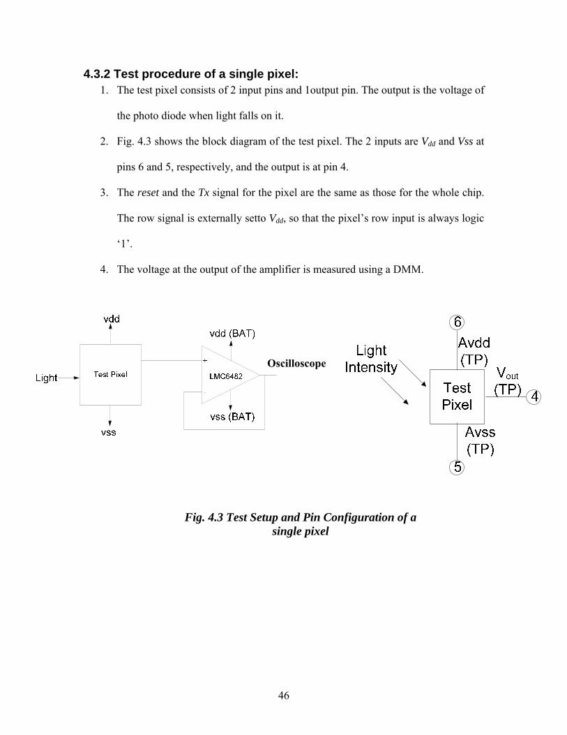
4.3.2 Test procedure of a single pixel: 1. The test pixel consists of 2 input pins and 1output pin. The output is the voltage of
the photo diode when light falls on it.
2. Fig. 4.3 shows the block diagram of the test pixel. The 2 inputs are Vdd and Vss at
pins 6 and 5, respectively, and the output is at pin 4.
3. The reset and the Tx signal for the pixel are the same as those for the whole chip.
The row signal is externally setto Vdd, so that the pixel’s row input is always logic
‘1’.
4. The voltage at the output of the amplifier is measured using a DMM.
Fig. 4.3 Test Setup and Pin Configuration of a single pixel
Oscilloscope
47
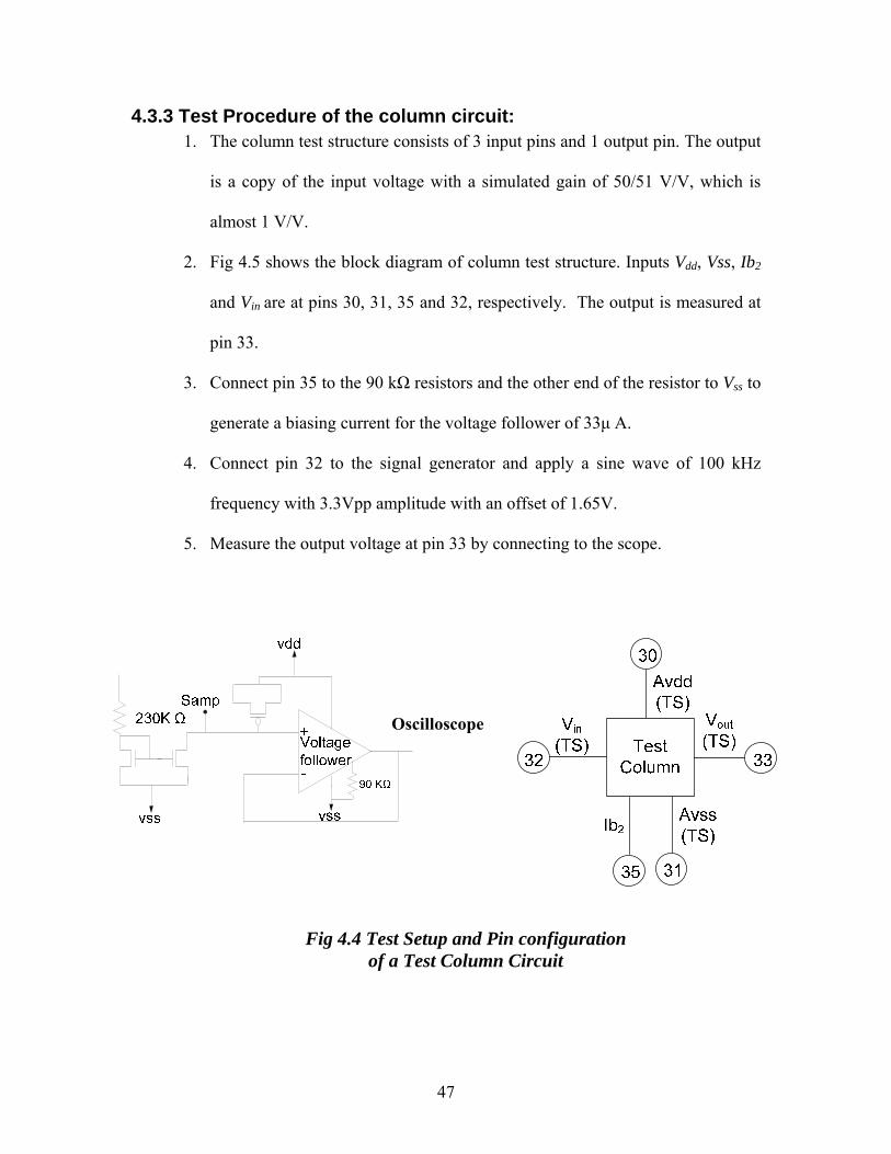
4.3.3 Test Procedure of the column circuit: 1. The column test structure consists of 3 input pins and 1 output pin. The output
is a copy of the input voltage with a simulated gain of 50/51 V/V, which is
almost 1 V/V.
2. Fig 4.5 shows the block diagram of column test structure. Inputs Vdd, Vss, Ib2
and Vin are at pins 30, 31, 35 and 32, respectively. The output is measured at
pin 33.
3. Connect pin 35 to the 90 kΩ resistors and the other end of the resistor to Vss to
generate a biasing current for the voltage follower of 33μ A.
4. Connect pin 32 to the signal generator and apply a sine wave of 100 kHz
frequency with 3.3Vpp amplitude with an offset of 1.65V.
5. Measure the output voltage at pin 33 by connecting to the scope.
Fig 4.4 Test Setup and Pin configuration of a Test Column Circuit
Oscilloscope
48
4.4 Data Acquisition System Setup: The output of the APS is a time-varying voltage (analog signal). In order
to regenerate an image from this signal a data acquisition system is necessary. The
data acquisition system consists of an A/D converter and a DE2 board. The A/D is
mounted and soldered on a prototype board along with a female header. The
female header is plugged into the DE2 board where the digital data from the A/D
converter is stored and later retrieved from the SRAM (one of the components of
DE2 board) by the user. The DE2 board consists of an FPGA, which is coded in
VHDL, to store the data from the A/D converter. The data which has been
retrieved from the DE2 board is analyzed by MATLAB for regeneration of the
image falling on the sensor.
4.4.1 A/D Setup 1. A 10-bit analog-to-digital converter which runs at a maximum speed of 30 Mega-
samples per second (MSPS) and has a power supply range from 3V to 5.5V is
used for the required data conversion. The part number is THS1030; it’s a Texas
Instrument’s product.
2. The digital data from the A/D converter is input to a DE2 board which has an
ALTERA Cyclone 2 FPGA.
3. The A/D used for data acquisition operated in 3 modes.
a. External Vref with single-ended input (MODE = Vss).
b. Internal Vref with differential input (MODE = Vdd/2).
c. Internal Vref with single-ended input (MODE = Vdd).
49
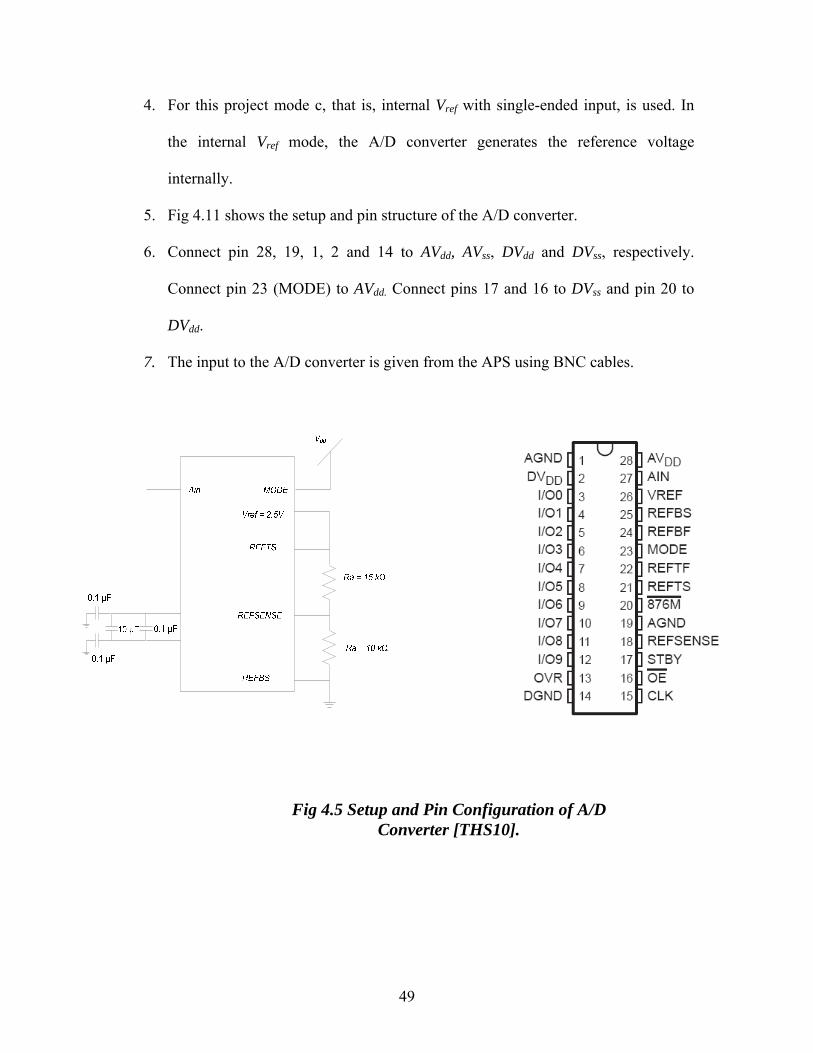
4. For this project mode c, that is, internal Vref with single-ended input, is used. In
the internal Vref mode, the A/D converter generates the reference voltage
internally.
5. Fig 4.11 shows the setup and pin structure of the A/D converter.
6. Connect pin 28, 19, 1, 2 and 14 to AVdd, AVss, DVdd and DVss, respectively.
Connect pin 23 (MODE) to AVdd. Connect pins 17 and 16 to DVss and pin 20 to
DVdd.
7. The input to the A/D converter is given from the APS using BNC cables.
Fig 4.5 Setup and Pin Configuration of A/D Converter [THS10].

50
4.4.2 Prototype Board Setup A 4 x 2.5 inch proto type board is used in the project to solder the A/D converter
and a 40 pin female header. The DE2 board has 40 pin male headers as one of the input
output source to the board. The 10-bit output data is soldered to the specified pins of the
header which will be later programmed on FPGA to store the exact format of the data in
SRAM (MSB to LSB). Along with A/D converter and the header the proto type board
even has 4 BNC pins. These 4 BNC pins are used to get Vdd, MSB of the counter in APS,
output of the sensor (Analog input to the A/D) and the clock signals. Same clock input is
given to the A/D converter, DE2 board and the APS.
4.4.3 DE2 Setup: 1. Inputs to the DE2 board are Q11, which is the MSB of the counter, clock, and the
digital output lines from A/D converter.
2. The digital data from the A/D converter is stored in SRAM using VHDL code
which is burned on the cyclone 2 FPGA in the DE2 board. Data sampling begins
on the rising edge of the counter MSB, Q11. The samples are taken on the rising
edge of the clock.
3. These values are stored in SRAM sequentially by incrementing the address. The
SRAM has an 18-bit address and 16-bit data in each address. Since the input is
only 10-bit data, the top 6 bits are padded with 0’s.
4. A *.sof file is generated when the code compiles successfully. This *.sof file is
used to burn onto the FPGA using the Quartus 2 software.
5. Quartus 2 software has a built-in DE2_control_pannel.sof file and a
DE2_control_pannel.exe file. Burning the DE2_control_pannel.sof file on the

51
FPGA and running the DE2_control_pannel.exe file on the host computer helps
the user to establish a direct access with the memory units on the DE2 board
(DMA) through a USB cable. This helps us to read the contents of the SRAM
directly without writing any VHDL code for reading.
7. The RAM contents are loaded into the host computer using the load file button on
the interface (DE2_control_pannel.exe) and it should be stored in .hex format.
8. The *.hex file stored can be opened using Notepad and the contents are viewed as
hexadecimal numbers line by line.
4.4.4Test Procedure for VHDL Code: 1. The VHDL code basic function is to store 2 values (photo and the reset value) for
each of the pixels. Since there are 1024 pixels, there 2048 values in total.
2. These 2048 values are stored in an SRAM chip through a FPGA, which is coded
in VHDL.
3. The VHDL code generates a process in which the address locations are increased
sequentially for every positive edge of the clock. The clock is the same for all the
circuits (APS, A/D converter and DE2 board).
4. The VHDL code is burned into the FPGA through a *.sof object file. Compiling
the VHDL code generates this object file. After the object file is generated, pins
are assigned for the input data using the DE2 data sheet.
5. The circuits should be powered on, in the following order: first the DE2 board is
powered on and the code is burnt on the FPGA. Then, the A/D converter is

52
switched on, followed by the APS, and finally the clock is given to all the circuits,
so as to avoid any loss of data.
6. The FPGA stores the data in SRAM as it is programmed.
7. Another built in *.sof file called DE2_control_pannel.sof is burnt on the FPGA
for retrieval of data from the SRAM.
8. The data is accessed using a software interface which is done by executing
DE2_control_pannel.exe. Using this interface, the data in SRAM is loaded into
the host computer with an extension *.HEX. This *.HEX file is viewed using the
Notepad application.
4.4.5 Test Procedure for MATLAB Code: 1. The *.HEX file stored on the host computer is opened using the MATLAB tool.
2. The MATLAB code first computes the correlated double sampling by taking the
difference between the reset and photo values of each pixel. Since the first 1024
values are photo values and the next 1024 are reset values, the difference between
the first and 1025th values, the second and 1026th value, and so on, are calculated.
3. Then the code normalizes the highest pixel value to number 255 (gray scale), so
that all the pixel values range between 0-255.
4. These values are arranged in a 32 x 32 matrix and plotted.

53
4.5 Test Procedure for the Active Pixel Sensor • The active pixel image sensor has 7 inputs and 2 outputs. The outputs are the
samples through Vout at a sample rate of 2 MHz frequency. These samples
need to be digitized and processed in order to regenerate the image incident on
the sensor.
• Correlated double sampling is the difference between the reset and the photo
samples. It is done in order to reduce noise. The types of noise that are
reduced due to correlated double sampling are fixed pattern noise (mismatch
in the source follower in each pixel) and flicker noise (low frequency noise).
• Fig 4.10 shows the basic block diagram of the APS which has to be tested.
The inputs of the chip are DVdd DVss AVdd AVss Ib1 Ib2 and clk. The outputs are
Vout and Q11.
• Connect pin 28, 19, 1, 2 and 14 to AVdd, AVss, DVdd and DVss, respectively.
• .Connect pin 20 to a signal generator which generates a 2 MHz clock.
• Connect pins 23 and 30 to 3.3 V and pins 24 and 31 to 0V.
• Connect pin 1 to a 2 kΩ resistor and the other end of the resistor to AVss to
generate a bias current of 33μA x 32 for the 32 voltage followers in column
circuits.
• Connect pin 2 to a 7 kΩ resistor and the other end of the resistor to AVdd to
generate a bias current of 11μA x 32 for the 32 column circuits.
• Connect the output Vout at pin 10 to the input in of the A/D converter and pin
19, Q11, to the DE2 Board using the BNC cables on the prototype board.

54
• Each part of the data acquisition system must be turned on in order to prevent
the loss of the data. First turn on the DE2 board and then burn the *.sof file on
it, then turn on A/D converter, followed by the APS, and finally connect clock
to all the circuits.
• After some time (after the data has been collected on the SRAM) turn off the
APS and D/A converter and then burn the DE2_control_pannel.sof file onto
the FPGA, followed by running the DE2_control_pannel.exe file to read the
data from SRAM.
• The DE2_control_pannel.exe software loads the contents of SRAM in *.HEX
format.
• The *.HEX file is analyzed using the MATLAB code for image regeneration.
Fig 4.6 Test Setup and Pin Configuration of Active Pixel Sensor.

55

56
5 Test Results and Conclusions
This chapter contains the test results of the test circuits and the APS based on
the test procedures discussed in chapter 4. Most of the signals are measured using an
oscilloscope and a snapshot of these results is presented in the report. For the active pixel
sensor, a snapshot of the image captured is presented.
5.1 Test Results of Test Photo Pixel The single photo pixel has Tx and reset signals that are generated internally by
the clock input. These signals are the same as the signals for the APS array. The test
setup and procedure for the single pixel is given in sections 4.4.1 and 4.4.2.
Fig 5.1 shows the output waveform of the single pixel on the oscilloscope and
fig 5.2 shows the MATLAB plot of the single pixel using a32 x 32 array used for testing
the entire array. The plot is done is order to verify the correctness of the code.
57
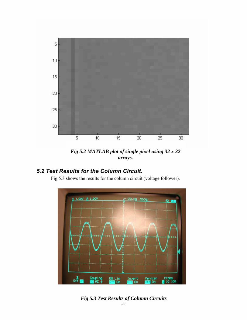
5.2 Test Results for the Column Circuit. Fig 5.3 shows the results for the column circuit (voltage follower).
Fig 5.1 Test Results of Single Pixel
Fig 5.2 MATLAB plot of single pixel using 32 x 32 arrays.
Fig 5.3 Test Results of Column Circuits

58
The output is lightly clamped due to the PMOS differential input. Only one bias
current (the bias current to the amplifier) is given to the circuit since we are testing only
the voltage follower. The input voltage is a sinusoidal wave with Vpp of 3.3V and input
frequency is 1 KHz. The result is seen in the oscilloscope.
5.3 Test Results of Digital Circuits Fig 5.4, 5.5 and 5.6 show the test results of the reset, Tx and row16 signals
respectively.
Since the digital signals control the APS, we must see correct functioning of
these signals. As discussed in section 4.3.1, a clock signal of 2MHz is given as input and
the output is measured using an oscilloscope. This waveform shows the working of the
reset, Tx and the row signals.
Fig 5.4 Test Results of the reset Signal at 1024μs

59
Fig 5.5 Test Results of the Tx Signal
Fig 5.6 Test Results of row16 Signal.

60
5.4 Test Results of Active Pixel Sensor 1. The setup for testing the APS is according to section 4.4.
2. In order to test real-time capture of an image, a laser beam of different sizes is
made incident using the optical laboratory at NMSU.
3. The optical equipment is already setup in the laboratory for various applications.
The APS is mounted in a box and the box is held on a stand in order to focus the
laser beam.
4. The lens is adjusted in such a way that the laser beam is focused on the center of
the array in order to capture the laser spot.
5. A laser beam with different sizes and at different positions is focused on the APS
and the DE2 captures this image data and plots the image using MATLAB.
6. Screenshots of these images are taken and presented in the following pages.
7. Fig 5.7 through 5.11 shows the list of test results of APS plotted in MATLAB.
Fig 5.7 MATLAB Test Result of APS picture 1

61
Fig 5.8 MATLAB Test Result of APS picture 2
Fig 5.9 MATLAB Test Result of APS picture 3

62
The dark line which appears on the 31st columns shows that there is a column
fail. The column fail is not due circuit, its due to the retrieval of the digital data from the
SRAM in the DE2 Board. The white spots in image indicate that the pixels have reached
to saturation. In future more constant light sourced should be used to have a uniform
image. A concave lens should be used to focus the image on the sensor in order to get
more accurately distinguishable image.
Fig 5.10 MATLAB Test Result of APS picture 4

63
5.5 Conclusions and Future Work
A 32 x 32 Active Pixel Sensor has been successfully designed, simulated, laid out and
sent for fabrication. The fabricated chip has been tested successfully by a low-cost
high-speed Data Acquisition System setup.
• The size of the pixel used in the array is 21μm x 21μm. In the future, the pixel
size should be reduced, so that integration times are longer and/or the pixel can
operate at higher light intensities.
• The A/D converter used in the test setup is very noisy. Careful setup, e.g.,
soldering and grounding, has to be done in order to make it work according to
specification.
• The retrieval of data from the SRAM includes some garbage data from the last 5
pixel values (only the reset values). The reason for this problem is that the A/D
converter architecture is a pipeline with a latency of 5 clock cycles. This problem
has to be fixed.
• The 29th row of the sensor seems to be not working; this problem seems to be a
layout issue and should be taken into consideration before the next design.
• The Data Acquisition System played a major role in testing the APS.
• The R256 logic did not work in testing since there was mistake in the logic. This
error must be corrected in the future work.
• There should be more precise MATLAB code for the regeneration of the image.

64
• In the future, images other than laser beams need to be captures with the image
sensor. This could be done by mounting a wide-angle lense in front of the chip,
so as to capture scenes from the office and/or laboratory.

65
REFERENCES [WHATI] The IT Encyclopedia and Learning Centre.
http://whatis.techtarget.com/definition/0,,sid9_gci213703,00.html, July 2001.
[WIKIP] The Free Encyclopedia. http://en.wikipedia.org/wiki/Image_sensor , July
2006. [SHORT] A Short Course in Choosing a Digital Camera.
http://www.shortcourses.com/choosing/sensors/05.htm, July 2006. [NOISE] Noise Sourced in CMOS Image Sensors. Hewlett-Packard Components
Group. Imaging Products Operations, January 1998. [DALSA] Image Sensor Architectures for Digital Cinematography. DALSA
technology with vision, March 2001. [MITA01] Mitani, Kohji, et al. Experimental Ultrahigh-Definition Color Camera
System with three 8M-pixel CCDs, SMPTE 143rd technical Conference and Exhibition, New York City, November 2001.
[COHE02] Marc Cohen, Gert Cauwenberghs, “Image Sharpness and Beam Focus
VLSI Sensors for Adaptive Optics”, IEEE Sensors Journal, vol. 2, no. 6, pp. 680-690, December 2002.
[WONG99] H.P.Wong, et al,, “CMOS Active Pixel Image Sensors Fabricated Using a
1.8-V, 0.25-μm CMOS Technology”, IEEE Trans, on Electron Devices, vol.45, no.4, April 1999.
[THS10] Data sheet for THS1030, Texas Instruments Incorporated. http://focus.ti.com/lit/ds/symlink/ths1030.pdf Copyright 1999-2003.
66
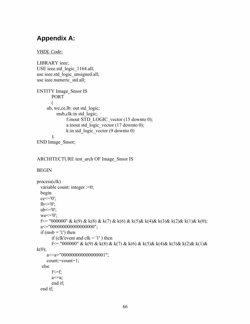
Appendix A: VHDL Code: LIBRARY ieee; USE ieee.std_logic_1164.all; use ieee.std_logic_unsigned.all; use ieee.numeric_std.all; ENTITY Image_Snsor IS PORT ( ub, we,ce,lb: out std_logic; msb,clk:in std_logic; f:inout STD_LOGIC_vector (15 downto 0); a:inout std_logic_vector (17 downto 0); k:in std_logic_vector (9 downto 0) ); END Image_Snsor; ARCHITECTURE test_arch OF Image_Snsor IS BEGIN process(clk) variable count: integer :=0; begin ce<='0'; lb<='0'; ub<='0'; we<='0'; f<= "000000" & k(9) & k(8) & k(7) & k(6) & k(5)& k(4)& k(3)& k(2)& k(1)& k(0); a<="000000000000000000"; if (msb = '1') then if (clk'event and clk = '1' ) then f<= "000000" & k(9) & k(8) & k(7) & k(6) & k(5)& k(4)& k(3)& k(2)& k(1)& k(0); a<=a+"000000000000000001"; count:=count+1; else f<=f; a<=a; end if; end if;

67
end process; END test_arch;

68
Appendix B: MATLAB Code: clc; clear all; fid=fopen('Image.hex','r'); A=fgetl(fid); tempd=[]; tempb=[]; while(A~=-1) D=hex2dec(A); B=dec2bin(D,16); A=fgetl(fid); tempb=[tempb;B]; tempd=[tempd;D]; end fclose(fid); tempb; tempd; x=tempd(1:1024); k=1; for ii=1:32 for jj=1:32 samp1(ii,jj)=x(k,1); k=k+1; end end samp1 y=tempd(1025:2048); k=1; for ii=1:32 for jj=1:32 reset(ii,jj)=y(k,1); k=k+1; end end reset pic = reset - samp1; colormap(gray); imagesc(pic);