36-V, Low-Capacitance, Low-Charge-Injection, Precision ... · 18-Jan-2018 Addendum-Page 1 PACKAGING...
41
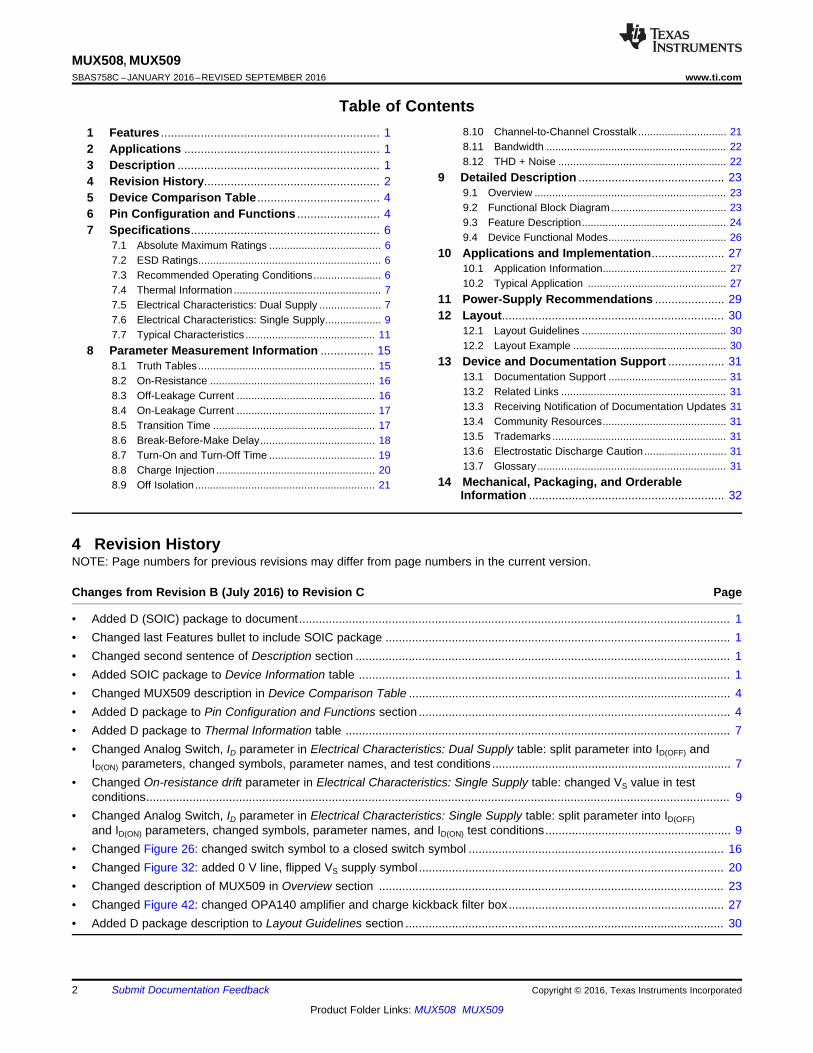
ADC VINP VINM Analog Inputs LED Photo Detector Bridge Sensor Thermocouple Current Sensing Optical Sensor PGA/INA + – MUX509 Copyright © 2016, Texas Instruments Incorporated –2 –1 0 1 2 –15 –10 –5 0 5 10 15 Charge Injection (pC) Source Voltage (V) C008 V DD = 12 V V SS = 0 V V DD = 10 V V SS = –10 V V DD = 15 V V SS = –15 V Product Folder Sample & Buy Technical Documents Tools & Software Support & Community Reference Design An IMPORTANT NOTICE at the end of this data sheet addresses availability, warranty, changes, use in safety-critical applications, intellectual property matters and other important disclaimers. PRODUCTION DATA. MUX508, MUX509 SBAS758C – JANUARY 2016 – REVISED SEPTEMBER 2016 MUX50x 36-V, Low-Capacitance, Low-Charge-Injection, Precision, Analog Multiplexers 1 1 Features 1• Low On-Capacitance – MUX508: 9.4 pF – MUX509: 6.7 pF • Low Input Leakage: 10 pA • Low Charge Injection: 0.3 pC • Rail-to-Rail Operation • Wide Supply Range: ±5 V to ±18 V, 10 V to 36 V • Low On-Resistance: 125 Ω • Transition Time: 92 ns • Break-Before-Make Switching Action • EN Pin Connectable to V DD • Logic Levels: 2 V to V DD • Low Supply Current: 45 μA • ESD Protection HBM: 2000 V • Industry-Standard TSSOP and SOIC Packages 2 Applications • Factory Automation and Industrial Process Controls • Programmable Logic Controllers (PLC) • Analog Input Modules • ATE Test Equipment • Digital Multimeters • Battery Monitoring Systems 3 Description The MUX508 and MUX509 (MUX50x) are modern, complementary metal-oxide semiconductor (CMOS), analog multiplexers (muxes). The MUX508 offers 8:1 single-ended channels, whereas the MUX509 offers differential 4:1 or dual 4:1 single-ended channels. The MUX508 and MUX509 work equally well with either dual supplies (±5 V to ±18 V) or a single supply (10 V to 36 V). They also perform well with symmetric supplies (such as V DD = 12 V, V SS = –12 V), and unsymmetric supplies (such as V DD = 12 V, V SS = –5 V). All digital inputs have TTL-logic compatible thresholds, ensuring both TTL and CMOS logic compatibility when operating in the valid supply voltage range. The MUX508 and MUX509 have very low on and off leakage currents, allowing these multiplexers to switch signals from high input impedance sources with minimal error. A low supply current of 45 μA allows for use in portable applications. Device Information (1) PART NUMBER PACKAGE BODY SIZE (NOM) MUX50x TSSOP (16) 5.00 mm × 4.40 mm SOIC (16) 9.90 mm × 3.91 mm (1) For all available packages, see the package option addendum at the end of the data sheet. Simplified Schematic Charge Injection vs Source Voltage
Transcript of 36-V, Low-Capacitance, Low-Charge-Injection, Precision ... · 18-Jan-2018 Addendum-Page 1 PACKAGING...

ADC
VINP
VINM
Analog Inputs
LED Photo Detector
Bridge Sensor
Thermocouple
Current Sensing
Optical Sensor
PGA/INA
+
±
MUX509
Copyright © 2016, Texas Instruments Incorporated
±2
±1
0
1
2
±15 ±10 ±5 0 5 10 15
Cha
rge
Inje
ctio
n (p
C)
Source Voltage (V) C008
VDD = 12 V VSS = 0 V
VDD = 10 V VSS = ±10 V
VDD = 15 V VSS = ±15 V
Product
Folder
Sample &Buy
Technical
Documents
Tools &
Software
Support &Community
ReferenceDesign
An IMPORTANT NOTICE at the end of this data sheet addresses availability, warranty, changes, use in safety-critical applications,intellectual property matters and other important disclaimers. PRODUCTION DATA.
MUX508, MUX509SBAS758C –JANUARY 2016–REVISED SEPTEMBER 2016
MUX50x36-V, Low-Capacitance, Low-Charge-Injection, Precision, Analog Multiplexers
1
1 Features1• Low On-Capacitance
– MUX508: 9.4 pF– MUX509: 6.7 pF
• Low Input Leakage: 10 pA• Low Charge Injection: 0.3 pC• Rail-to-Rail Operation• Wide Supply Range: ±5 V to ±18 V, 10 V to 36 V• Low On-Resistance: 125 Ω• Transition Time: 92 ns• Break-Before-Make Switching Action• EN Pin Connectable to VDD
• Logic Levels: 2 V to VDD
• Low Supply Current: 45 µA• ESD Protection HBM: 2000 V• Industry-Standard TSSOP and SOIC Packages
2 Applications• Factory Automation and Industrial Process
Controls• Programmable Logic Controllers (PLC)• Analog Input Modules• ATE Test Equipment• Digital Multimeters• Battery Monitoring Systems
3 DescriptionThe MUX508 and MUX509 (MUX50x) are modern,complementary metal-oxide semiconductor (CMOS),analog multiplexers (muxes). The MUX508 offers 8:1single-ended channels, whereas the MUX509 offersdifferential 4:1 or dual 4:1 single-ended channels. TheMUX508 and MUX509 work equally well with eitherdual supplies (±5 V to ±18 V) or a single supply (10 Vto 36 V). They also perform well with symmetricsupplies (such as VDD = 12 V, VSS = –12 V), andunsymmetric supplies (such as VDD = 12 V, VSS =–5 V). All digital inputs have TTL-logic compatiblethresholds, ensuring both TTL and CMOS logiccompatibility when operating in the valid supplyvoltage range.
The MUX508 and MUX509 have very low on and offleakage currents, allowing these multiplexers toswitch signals from high input impedance sourceswith minimal error. A low supply current of 45 µAallows for use in portable applications.
Device Information(1)
PART NUMBER PACKAGE BODY SIZE (NOM)
MUX50xTSSOP (16) 5.00 mm × 4.40 mmSOIC (16) 9.90 mm × 3.91 mm
(1) For all available packages, see the package option addendumat the end of the data sheet.
Simplified Schematic Charge Injection vs Source Voltage
2
MUX508, MUX509SBAS758C –JANUARY 2016–REVISED SEPTEMBER 2016 www.ti.com
Product Folder Links: MUX508 MUX509
Submit Documentation Feedback Copyright © 2016, Texas Instruments Incorporated
Table of Contents1 Features .................................................................. 12 Applications ........................................................... 13 Description ............................................................. 14 Revision History..................................................... 25 Device Comparison Table ..................................... 46 Pin Configuration and Functions ......................... 47 Specifications......................................................... 6
7.1 Absolute Maximum Ratings ...................................... 67.2 ESD Ratings.............................................................. 67.3 Recommended Operating Conditions....................... 67.4 Thermal Information .................................................. 77.5 Electrical Characteristics: Dual Supply ..................... 77.6 Electrical Characteristics: Single Supply................... 97.7 Typical Characteristics ............................................ 11
8 Parameter Measurement Information ................ 158.1 Truth Tables ............................................................ 158.2 On-Resistance ........................................................ 168.3 Off-Leakage Current ............................................... 168.4 On-Leakage Current ............................................... 178.5 Transition Time ....................................................... 178.6 Break-Before-Make Delay....................................... 188.7 Turn-On and Turn-Off Time .................................... 198.8 Charge Injection ...................................................... 208.9 Off Isolation............................................................. 21
8.10 Channel-to-Channel Crosstalk .............................. 218.11 Bandwidth ............................................................. 228.12 THD + Noise ......................................................... 22
9 Detailed Description ............................................ 239.1 Overview ................................................................. 239.2 Functional Block Diagram ....................................... 239.3 Feature Description................................................. 249.4 Device Functional Modes........................................ 26
10 Applications and Implementation...................... 2710.1 Application Information.......................................... 2710.2 Typical Application ............................................... 27
11 Power-Supply Recommendations ..................... 2912 Layout................................................................... 30
12.1 Layout Guidelines ................................................. 3012.2 Layout Example .................................................... 30
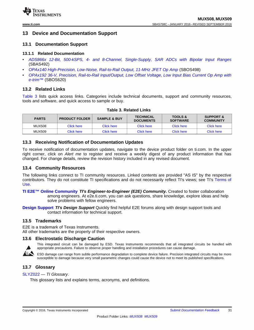
13 Device and Documentation Support ................. 3113.1 Documentation Support ........................................ 3113.2 Related Links ........................................................ 3113.3 Receiving Notification of Documentation Updates 3113.4 Community Resources.......................................... 3113.5 Trademarks ........................................................... 3113.6 Electrostatic Discharge Caution............................ 3113.7 Glossary ................................................................ 31
14 Mechanical, Packaging, and OrderableInformation ........................................................... 32
4 Revision HistoryNOTE: Page numbers for previous revisions may differ from page numbers in the current version.
Changes from Revision B (July 2016) to Revision C Page
• Added D (SOIC) package to document.................................................................................................................................. 1• Changed last Features bullet to include SOIC package ........................................................................................................ 1• Changed second sentence of Description section ................................................................................................................. 1• Added SOIC package to Device Information table ................................................................................................................ 1• Changed MUX509 description in Device Comparison Table ................................................................................................. 4• Added D package to Pin Configuration and Functions section .............................................................................................. 4• Added D package to Thermal Information table .................................................................................................................... 7• Changed Analog Switch, ID parameter in Electrical Characteristics: Dual Supply table: split parameter into ID(OFF) and
ID(ON) parameters, changed symbols, parameter names, and test conditions........................................................................ 7• Changed On-resistance drift parameter in Electrical Characteristics: Single Supply table: changed VS value in test
conditions................................................................................................................................................................................ 9• Changed Analog Switch, ID parameter in Electrical Characteristics: Single Supply table: split parameter into ID(OFF)
and ID(ON) parameters, changed symbols, parameter names, and ID(ON) test conditions........................................................ 9• Changed Figure 26: changed switch symbol to a closed switch symbol ............................................................................. 16• Changed Figure 32: added 0 V line, flipped VS supply symbol............................................................................................ 20• Changed description of MUX509 in Overview section ........................................................................................................ 23• Changed Figure 42: changed OPA140 amplifier and charge kickback filter box................................................................. 27• Added D package description to Layout Guidelines section ................................................................................................ 30

3
MUX508, MUX509www.ti.com SBAS758C –JANUARY 2016–REVISED SEPTEMBER 2016
Product Folder Links: MUX508 MUX509
Submit Documentation FeedbackCopyright © 2016, Texas Instruments Incorporated
Changes from Revision A (March 2016) to Revision B Page
• Added TI Design .................................................................................................................................................................... 1• Changed Analog Switch, IS(OFF) and ID parameter specifications in Electrical Characteristics: Single Supply table.............. 9
Changes from Original (January 2016) to Revision A Page
• Changed from product preview to production data ................................................................................................................ 1

1A0 16 A1
2EN 15 A2
3VSS 14 GND
4S1 13 VDD
5S2 12 S5
6S3 11 S6
7S4 10 S7
8D 9 S8
4
MUX508, MUX509SBAS758C –JANUARY 2016–REVISED SEPTEMBER 2016 www.ti.com
Product Folder Links: MUX508 MUX509
Submit Documentation Feedback Copyright © 2016, Texas Instruments Incorporated
5 Device Comparison Table
PRODUCT DESCRIPTIONMUX508 8-channel, single-ended analog multiplexer (8:1 mux)MUX509 4-channel differential or dual 4:1 single-ended analog multiplexer (8:2 mux)
6 Pin Configuration and Functions
MUX508: PW and D Packages16-Pin TSSOP and SOIC
Top View
Pin Functions: MUX508PIN
TYPE DESCRIPTIONNAME NO.A0 1 Digital input Address line 0A1 16 Digital input Address line 1A2 15 Digital input Address line 2D 8 Analog input or output Drain pin. Can be an input or output.
EN 2 Digital input Active high digital input. When this pin is low, all switches are turned off. When this pin ishigh, the A[2:0] logic inputs determine which switch is turned on.
GND 14 Power supply Ground (0 V) referenceS1 4 Analog input or output Source pin 1. Can be an input or output.S2 5 Analog input or output Source pin 2. Can be an input or output.S3 6 Analog input or output Source pin 3. Can be an input or output.S4 7 Analog input or output Source pin 4. Can be an input or output.S5 12 Analog input or output Source pin 5. Can be an input or output.S6 11 Analog input or output Source pin 6. Can be an input or output.S7 10 Analog input or output Source pin 7. Can be an input or output.S8 9 Analog input or output Source pin 8. Can be an input or output.
VDD 13 Power supplyPositive power supply. This pin is the most positive power-supply potential. For reliableoperation, connect a decoupling capacitor ranging from 0.1 µF to 10 µF between VDDand GND.
VSS 3 Power supplyNegative power supply. This pin is the most negative power-supply potential. In single-supply applications, this pin can be connected to ground. For reliable operation, connect adecoupling capacitor ranging from 0.1 µF to 10 µF between VSS and GND.

1A0 16 A1
2EN 15 GND
3VSS 14 VDD
4S1A 13 S1B
5S2A 12 S2B
6S3A 11 S3B
7S4A 10 S4B
8DA 9 DB
5
MUX508, MUX509www.ti.com SBAS758C –JANUARY 2016–REVISED SEPTEMBER 2016
Product Folder Links: MUX508 MUX509
Submit Documentation FeedbackCopyright © 2016, Texas Instruments Incorporated
MUX509: PW and D Packages16-Pin TSSOP and SOIC
Top View
Pin Functions: MUX509PIN
TYPE DESCRIPTIONNAME NO.A0 1 Digital input Address line 0A1 16 Digital input Address line 1DA 8 Analog input or output Drain pin A. Can be an input or output.DB 9 Analog input or output Drain pin B. Can be an input or output.
EN 2 Digital input Active high digital input. When this pin is low, all switches are turned off. When this pin ishigh, the A[1:0] logic inputs determine which pair of switches is turned on.
GND 15 Power supply Ground (0 V) referenceS1A 4 Analog input or output Source pin 1A. Can be an input or output.S2A 5 Analog input or output Source pin 2A. Can be an input or output.S3A 6 Analog input or output Source pin 3A. Can be an input or output.S4A 7 Analog input or output Source pin 4A. Can be an input or output.S1B 13 Analog input or output Source pin 1B. Can be an input or output.S2B 12 Analog input or output Source pin 2B. Can be an input or output.S3B 11 Analog input or output Source pin 3B. Can be an input or output.S4B 10 Analog input or output Source pin 4B. Can be an input or output.
VDD 14 Power supplyPositive power supply. This pin is the most positive power supply potential. For reliableoperation, connect a decoupling capacitor ranging from 0.1 µF to 10 µF between VDDand GND.
VSS 3 Power supplyNegative power supply. This pin is the most negative power supply potential. In single-supply applications, this pin can be connected to ground. For reliable operation, connect adecoupling capacitor ranging from 0.1 µF to 10 µF between VSS and GND.

6
MUX508, MUX509SBAS758C –JANUARY 2016–REVISED SEPTEMBER 2016 www.ti.com
Product Folder Links: MUX508 MUX509
Submit Documentation Feedback Copyright © 2016, Texas Instruments Incorporated
(1) Stresses beyond those listed under Absolute Maximum Ratings may cause permanent damage to the device. These are stress ratingsonly, which do not imply functional operation of the device at these or any other conditions beyond those indicated under RecommendedOperating Conditions. Exposure to absolute-maximum-rated conditions for extended periods may affect device reliability.
(2) Only one pin at a time
7 Specifications
7.1 Absolute Maximum Ratingsover operating free-air temperature range (unless otherwise noted) (1)
MIN MAX UNIT
Supply voltageVDD –0.3 40
VVSS –40 0.3VDD – VSS 40
Digital input pins (2) EN, A0, A1, A2 pinsVoltage VSS – 0.3 VDD + 0.3 VCurrent –30 30 mA
Analog input pins (2) Sx, SxA, SxB pinsVoltage VSS – 2 VDD + 2 VCurrent –30 30 mA
Analog output pins (2) D, DA, DB pinsVoltage VSS – 2 VDD + 2 VCurrent –30 30 mA
TemperatureOperating, TA –55 150
°CJunction, TJ 150Storage, Tstg –65 150
(1) JEDEC document JEP155 states that 500-V HBM allows safe manufacturing with a standard ESD control process.(2) JEDEC document JEP157 states that 250-V CDM allows safe manufacturing with a standard ESD control process.
7.2 ESD RatingsVALUE UNIT
V(ESD) Electrostatic dischargeHuman-body model (HBM), per ANSI/ESDA/JEDEC JS-001 (1) 2000
VCharged-device model (CDM), per JEDEC specification JESD22-C101 (2) 500
(1) When VSS = 0 V, VDD can range from 10 V to 36 V.(2) VDD and VSS can be any value as long as 10 V ≤ (VDD – VSS) ≤ 36 V, and VDD ≥ 5 V.(3) VS is the voltage on all the S pins.
7.3 Recommended Operating ConditionsMIN NOM MAX UNIT
VDD(1) Positive power-supply voltage
Dual supply 5 18V
Single supply 10 36VSS
(2) Negative power-supply voltage (dual supply) –5 –18 VVDD – VSS Supply voltage 10 36 VVS Source pins voltage (3) VSS VDD VVD Drain pins voltage VSS VDD VVEN Enable pin voltage VSS VDD VVA Address pins voltage VSS VDD VICH Channel current (TA = 25°C) –25 25 mATA Operating temperature –40 125 °C
7
MUX508, MUX509www.ti.com SBAS758C –JANUARY 2016–REVISED SEPTEMBER 2016
Product Folder Links: MUX508 MUX509
Submit Documentation FeedbackCopyright © 2016, Texas Instruments Incorporated
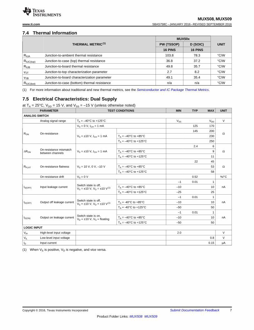
(1) For more information about traditional and new thermal metrics, see the Semiconductor and IC Package Thermal Metrics.
7.4 Thermal Information
THERMAL METRIC (1)MUX50x
UNITPW (TSSOP) D (SOIC)16 PINS 16 PINS
RθJA Junction-to-ambient thermal resistance 103.8 78.3 °C/WRθJC(top) Junction-to-case (top) thermal resistance 36.8 37.2 °C/WRθJB Junction-to-board thermal resistance 49.8 35.7 °C/WψJT Junction-to-top characterization parameter 2.7 8.2 °C/WψJB Junction-to-board characterization parameter 49.1 35.4 °C/WRθJC(bot) Junction-to-case (bottom) thermal resistance n/a n/a °C/W
(1) When VS is positive, VD is negative, and vice versa.
7.5 Electrical Characteristics: Dual Supplyat TA = 25°C, VDD = 15 V, and VSS = –15 V (unless otherwise noted)
PARAMETER TEST CONDITIONS MIN TYP MAX UNIT
ANALOG SWITCH
Analog signal range TA = –40°C to +125°C VSS VDD V
RON On-resistance
VS = 0 V, ICH = 1 mA 125 170
ΩVS = ±10 V, ICH = 1 mA
145 200
TA = –40°C to +85°C 230
TA = –40°C to +125°C 250
ΔRONOn-resistance mismatchbetween channels VS = ±10 V, ICH = 1 mA
2.4 6
ΩTA = –40°C to +85°C 9
TA = –40°C to +125°C 11
RFLAT On-resistance flatness VS = 10 V, 0 V, –10 V
22 45
ΩTA = –40°C to +85°C 53
TA = –40°C to +125°C 58
On-resistance drift VS = 0 V 0.52 %/°C
IS(OFF) Input leakage current Switch state is off,VS = ±10 V, VD = ±10 V (1)
–1 0.01 1
nATA = –40°C to +85°C –10 10
TA = –40°C to +125°C –25 25
ID(OFF) Output off leakage current Switch state is off,VS = ±10 V, VD = ±10 V (1)
–1 0.01 1
nATA = -40°C to +85°C –10 10
TA = -40°C to +125°C –50 50
ID(ON) Output on leakage current Switch state is on,VD = ±10 V, VS = floating
–1 0.01 1
nATA = –40°C to +85°C –10 10
TA = –40°C to +125°C –50 50
LOGIC INPUT
VIH High-level input voltage 2.0 V
VIL Low-level input voltage 0.8 V
ID Input current 0.15 µA
8
MUX508, MUX509SBAS758C –JANUARY 2016–REVISED SEPTEMBER 2016 www.ti.com
Product Folder Links: MUX508 MUX509
Submit Documentation Feedback Copyright © 2016, Texas Instruments Incorporated
Electrical Characteristics: Dual Supply (continued)at TA = 25°C, VDD = 15 V, and VSS = –15 V (unless otherwise noted)
PARAMETER TEST CONDITIONS MIN TYP MAX UNIT
(2) Specified by design, not production tested.
SWITCH DYNAMICS (2)
tON Enable turn-on time VS = ±10 V, RL = 300 Ω,CL= 35 pF
88 136
nsTA = –40°C to +85°C 144
TA = –40°C to +125°C 151
tOFF Enable turn-off time VS = ±10 V, RL = 300 Ω,CL= 35 pF
63 75
nsTA = –40°C to +85°C 83
TA = –40°C to +125°C 90
tt Transition time VS = 10 V, RL = 300 Ω,CL= 35 pF,
92 143
nsTA = –40°C to +85°C 151
TA = –40°C to +125°C 157
tBBMBreak-before-make timedelay VS = 10 V, RL = 300 Ω, CL= 35 pF, TA = –40°C to +125°C 30 54 ns
QJ Charge injection CL = 1 nF, RS = 0 ΩVS = 0 V 0.3
pCVS = –15 V to +15 V ±0.6
Off-isolation RL = 50 Ω, VS = 1 VRMS,f = 1 MHz
Nonadjacent channel to D, DA, DB –96dB
Adjacent channel to D, DA, DB –85
Channel-to-channelcrosstalk
RL = 50 Ω, VS = 1 VRMS,f = 1 MHz
Nonadjacent channels –96dB
Adjacent channels –88
CS(OFF) Input off-capacitance f = 1 MHz, VS = 0 V 2.4 2.9 pF
CD(OFF) Output off-capacitance f = 1 MHz, VS = 0 VMUX508 7.5 8.4
pFMUX509 4.3 5
CD(ON)Input/Output on-capacitance f = 1 MHz, VS = 0 V
MUX508 9.4 10.6pF
MUX509 6.7 7.7
POWER SUPPLY
VDD supply current All VA = 0 V or 3.3 V,VS = 0 V, VEN = 3.3 V,
45 59
µATA = –40°C to +85°C 62
TA = –40°C to +125°C 83
VSS supply current All VA = 0 V or 3.3 V,VS = 0 V, VEN = 3.3 V,
25 34
µATA = –40°C to +85°C 37
TA = –40°C to +125°C 57
9
MUX508, MUX509www.ti.com SBAS758C –JANUARY 2016–REVISED SEPTEMBER 2016
Product Folder Links: MUX508 MUX509
Submit Documentation FeedbackCopyright © 2016, Texas Instruments Incorporated
(1) Specified by design, not production tested.(2) When VS is 1 V, VD is 10 V, and vice versa.
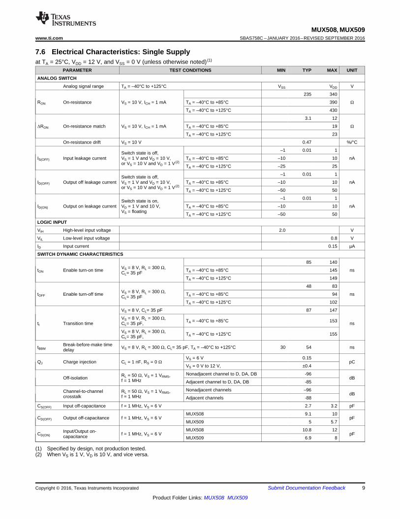
7.6 Electrical Characteristics: Single Supplyat TA = 25°C, VDD = 12 V, and VSS = 0 V (unless otherwise noted) (1)
PARAMETER TEST CONDITIONS MIN TYP MAX UNIT
ANALOG SWITCH
Analog signal range TA = –40°C to +125°C VSS VDD V
RON On-resistance VS = 10 V, ICH = 1 mA
235 340
ΩTA = –40°C to +85°C 390
TA = –40°C to +125°C 430
ΔRON On-resistance match VS = 10 V, ICH = 1 mA
3.1 12
ΩTA = –40°C to +85°C 19
TA = –40°C to +125°C 23
On-resistance drift VS = 10 V 0.47 %/°C
IS(OFF) Input leakage currentSwitch state is off,VS = 1 V and VD = 10 V,or VS = 10 V and VD = 1 V (2)
–1 0.01 1
nATA = –40°C to +85°C –10 10
TA = –40°C to +125°C –25 25
ID(OFF) Output off leakage currentSwitch state is off,VS = 1 V and VD = 10 V,or VS = 10 V and VD = 1 V (2)
–1 0.01 1
nATA = –40°C to +85°C –10 10
TA = –40°C to +125°C –50 50
ID(ON) Output on leakage currentSwitch state is on,VD = 1 V and 10 V,VS = floating
–1 0.01 1
nATA = –40°C to +85°C –10 10
TA = –40°C to +125°C –50 50
LOGIC INPUT
VIH High-level input voltage 2.0 V
VIL Low-level input voltage 0.8 V
ID Input current 0.15 µA
SWITCH DYNAMIC CHARACTERISTICS
tON Enable turn-on time VS = 8 V, RL = 300 Ω,CL= 35 pF
85 140
nsTA = –40°C to +85°C 145
TA = –40°C to +125°C 149
tOFF Enable turn-off time VS = 8 V, RL = 300 Ω,CL= 35 pF
48 83
nsTA = –40°C to +85°C 94
TA = –40°C to +125°C 102
tt Transition time
VS = 8 V, CL= 35 pF 87 147
nsVS = 8 V, RL = 300 Ω,CL= 35 pF, TA = –40°C to +85°C 153
VS = 8 V, RL = 300 Ω,CL= 35 pF, TA = –40°C to +125°C 155
tBBMBreak-before-make timedelay VS = 8 V, RL = 300 Ω, CL= 35 pF, TA = –40°C to +125°C 30 54 ns
QJ Charge injection CL = 1 nF, RS = 0 ΩVS = 6 V 0.15
pCVS = 0 V to 12 V, ±0.4
Off-isolation RL = 50 Ω, VS = 1 VRMS,f = 1 MHz
Nonadjacent channel to D, DA, DB -96dB
Adjacent channel to D, DA, DB -85
Channel-to-channelcrosstalk
RL = 50 Ω, VS = 1 VRMS,f = 1 MHz
Nonadjacent channels –96dB
Adjacent channels -88
CS(OFF) Input off-capacitance f = 1 MHz, VS = 6 V 2.7 3.2 pF
CD(OFF) Output off-capacitance f = 1 MHz, VS = 6 VMUX508 9.1 10
pFMUX509 5 5.7
CD(ON)Input/Output on-capacitance f = 1 MHz, VS = 6 V
MUX508 10.8 12pF
MUX509 6.9 8

10
MUX508, MUX509SBAS758C –JANUARY 2016–REVISED SEPTEMBER 2016 www.ti.com
Product Folder Links: MUX508 MUX509
Submit Documentation Feedback Copyright © 2016, Texas Instruments Incorporated
Electrical Characteristics: Single Supply (continued)at TA = 25°C, VDD = 12 V, and VSS = 0 V (unless otherwise noted)(1)
PARAMETER TEST CONDITIONS MIN TYP MAX UNIT
POWER SUPPLY
VDD supply current All VA = 0 V or 3.3 V,VS= 0 V, VEN = 3.3 V
42 53
µATA = –40°C to +85°C 56
TA = –40°C to +125°C 77
VSS supply current All VA = 0 V or 3.3 V,VS = 0 V, VEN = 3.3 V
23 38
µATA = –40°C to +85°C 31
TA = –40°C to +125°C 51
0
50
100
150
200
250
0 6 12 18 24 30 36
On
Res
ista
nce
(�)
Source or Drain Voltage (V) C023
VDD = 30 V VSS = 0 V
VDD = 33 V VSS = 0 V
VDD = 36 V VSS = 0 V
0
100
200
300
400
500
600
700
0 2 4 6 8 10 12 14
On
Res
ista
nce
(�)
Source or Drain Voltage (V) C005
VDD = 14 V VSS = 0 V
VDD = 12 V VSS = 0 V
VDD = 10 V VSS = 0 V
0
100
200
300
400
500
600
700
±8 ±6 ±4 ±2 0 2 4 6 8
On
Res
ista
nce
(�)
Source or Drain Voltage (V) C003
VDD = 5 V VSS = ±5 V
VDD = 6 V VSS = ±6 V
VDD = 7 V VSS = ±7 V
0
100
200
300
400
500
600
700
0 2 4 6 8 10 12
On
Res
ista
nce
(�)
Source or Drain Voltage (V) C004
TA = ±40�C TA = 0�C
TA = 125�C TA = 85�C
TA = 25�C
0
50
100
150
200
250
±20 ±15 ±10 ±5 0 5 10 15 20
On
Res
ista
nce
(�)
Source or Drain Voltage (V) C001
VDD = 15 V VSS = ±15 V
VDD = 18 V VSS = ±18 V
VDD = 16.5 V VSS = ±16.5 V
VDD = 13.5 V VSS = ±13.5 V
0
50
100
150
200
250
±18 ±12 ±6 0 6 12 18
On
Res
ista
nce
(�)
Source or Drain Voltage (V) C002
TA = ±40�C TA = 0�C
TA = 125�C TA = 85�C
TA = 25�C
11
MUX508, MUX509www.ti.com SBAS758C –JANUARY 2016–REVISED SEPTEMBER 2016
Product Folder Links: MUX508 MUX509
Submit Documentation FeedbackCopyright © 2016, Texas Instruments Incorporated
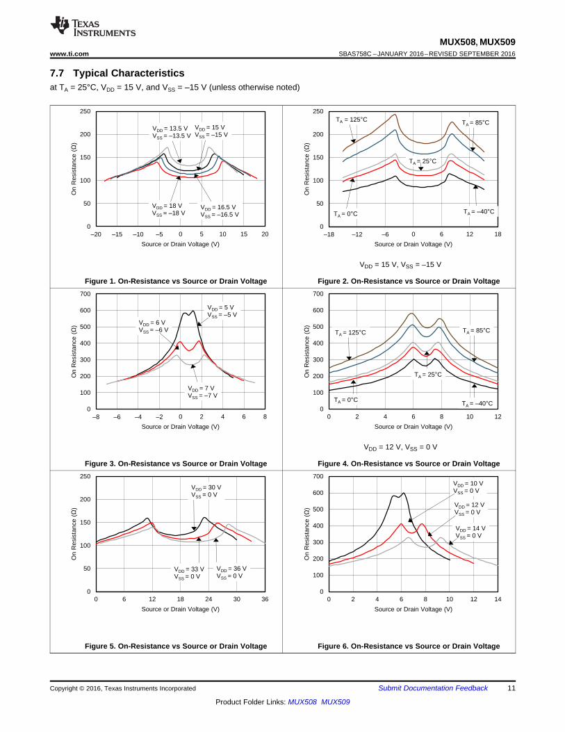
7.7 Typical Characteristicsat TA = 25°C, VDD = 15 V, and VSS = –15 V (unless otherwise noted)
Figure 1. On-Resistance vs Source or Drain Voltage
VDD = 15 V, VSS = –15 V
Figure 2. On-Resistance vs Source or Drain Voltage
Figure 3. On-Resistance vs Source or Drain Voltage
VDD = 12 V, VSS = 0 V
Figure 4. On-Resistance vs Source or Drain Voltage
Figure 5. On-Resistance vs Source or Drain Voltage Figure 6. On-Resistance vs Source or Drain Voltage

±2
±1
0
1
2
±15 ±10 ±5 0 5 10 15
Cha
rge
Inje
ctio
n (p
C)
Source Voltage (V) C008
VDD = 12 V VSS = 0 V
VDD = 10 V VSS = ±10 V
VDD = 15 V VSS = ±15 V
±2
±1
0
1
2
±15 ±10 ±5 0 5 10 15
Cha
rge
Inje
ctio
n (p
C)
Source Voltage (V) C025
VDD = 12 V VSS = 0 V
VDD = 10 V VSS = ±10 V
VDD = 15 V VSS = ±15 V
±900
±600
±300
0
300
600
900
±75 ±50 ±25 0 25 50 75 100 125 150
Leak
age
Cur
rent
(pA
)
Temperature (�C) C006
ID(ON)+
ID(OFF)+
IS(OFF)+
IS(OFF)±
ID(OFF)±
ID(ON)±
±900
±600
±300
0
300
600
900
±75 ±50 ±25 0 25 50 75 100 125 150
Leak
age
Cur
rent
(pA
)
Temperature (�C) C007
IS(OFF)+
ID(OFF)+
ID(ON)+
IS(OFF)±
ID(OFF)± ID(ON)±
0
50
100
150
200
250
0 6 12 18 24
On
Res
ista
nce
(�)
Source or Drain Voltage (V) C029
0
50
100
150
200
250
±12 ±6 0 6 12
On
Res
ista
nce
(�)
Source or Drain Voltage (V) C024
12
MUX508, MUX509SBAS758C –JANUARY 2016–REVISED SEPTEMBER 2016 www.ti.com
Product Folder Links: MUX508 MUX509
Submit Documentation Feedback Copyright © 2016, Texas Instruments Incorporated
Typical Characteristics (continued)at TA = 25°C, VDD = 15 V, and VSS = –15 V (unless otherwise noted)
VDD = 24 V, VSS = 0 V
Figure 7. On-Resistance vs Source or Drain Voltage
VDD = 12 V, VSS = –12 V
Figure 8. On-Resistance vs Source or Drain Voltage
VDD = 15 V, VSS = –15 V
Figure 9. Leakage Current vs Temperature
VDD = 12 V, VSS = 0 V
Figure 10. Leakage Current vs Temperature
MUX508, source-to-drain
Figure 11. Charge Injection vs Source Voltage
MUX509, source-to-drain
Figure 12. Charge Injection vs Source Voltage
0.01
0.1
1
10
100
10 100 1k 10k 100k
TH
D+
N (
%)
Frequency (Hz) C014
VDD = 15 V VSS = ±15 V
VDD = 5 V VSS = ±5 V
±9
±6
±3
0
3
100k 1M 10M 100M 1G
On
Res
pons
e (d
B)
Frequency (Hz) C018
±140
±120
±100
±80
±60
±40
±20
0
10k 100k 1M 10M 100M 1G
Off
Isol
atio
n (d
B)
Frequency (Hz) C012
Non-Adjacent Channel to D (Output)
Adjacent Channel to D (Output)
±140
±120
±100
±80
±60
±40
±20
0
10k 100k 1M 10M 100M 1G
Cro
ssta
lk (
dB)
Frequency (Hz) C013
Non-Adjacent Channels
Adjacent Channels
±9
±6
±3
0
3
6
9
±15 ±10 ±5 0 5 10 15
Cha
rge
Inje
ctio
n (p
C)
Drain voltage (V) C011
VDD = 12 V VSS = 0 V
VDD = 10 V VSS = ±10 V
VDD = 15 V VSS = ±15 V
0
30
60
90
120
150
±75 ±50 ±25 0 25 50 75 100 125 150
Tur
n O
n an
d T
urn
Off
Tim
es (
ns)
Temperature (�C) C010
tOFF (VDD = 15 V, VSS = ±15 V)
tON (VDD = 15 V, VSS = ±15 V)
tOFF (VDD = 12 V, VSS = 0 V)
tON (VDD = 12 V, VSS = 0 V)
13
MUX508, MUX509www.ti.com SBAS758C –JANUARY 2016–REVISED SEPTEMBER 2016
Product Folder Links: MUX508 MUX509
Submit Documentation FeedbackCopyright © 2016, Texas Instruments Incorporated
Typical Characteristics (continued)at TA = 25°C, VDD = 15 V, and VSS = –15 V (unless otherwise noted)
Drain-to-source
Figure 13. Charge Injection vs Source or Drain Voltage Figure 14. Turn-On and Turn-Off Times vs Temperature
Figure 15. Off Isolation vs Frequency Figure 16. Crosstalk vs Frequency
Figure 17. THD+N vs Frequency Figure 18. On Response vs Frequency

0
3
6
9
12
15
18
0 3 6 9 12
Cap
acita
nce
(pF
)
Source or Drain Voltage (V) C022
CD(OFF)
CD(ON)
CS(OFF)
0
3
6
9
12
15
18
0 3 6 9 12
Cap
acita
nce
(pF
)
Source or Drain Voltage (V) C027
CD(OFF)
CD(ON)
CS(OFF)
0
3
6
9
12
15
18
0 5 10 15 20 25 30
Cap
acita
nce
(pF
)
Source Voltage (V) C016
CD(OFF)
CD(ON)
CS(OFF)
0
3
6
9
12
15
18
0 5 10 15 20 25 30
Cap
acita
nce
(pF
)
Source or Drain Voltage (V) C028
CD(OFF)
CD(ON)
CS(OFF)
0
3
6
9
12
15
18
±15 ±10 ±5 0 5 10 15
Cap
acita
nce
(pF
)
Source Voltage (V) C015
CD(OFF)
CD(ON)
CS(OFF)
0
3
6
9
12
15
18
±15 ±10 ±5 0 5 10 15
Cap
acita
nce
(pF
)
Source or Drain Voltage (V) C026
CD(OFF)
CD(ON)
CS(OFF)
14
MUX508, MUX509SBAS758C –JANUARY 2016–REVISED SEPTEMBER 2016 www.ti.com
Product Folder Links: MUX508 MUX509
Submit Documentation Feedback Copyright © 2016, Texas Instruments Incorporated
Typical Characteristics (continued)at TA = 25°C, VDD = 15 V, and VSS = –15 V (unless otherwise noted)
MUX508, VDD = 15 V, VSS = –15 V
Figure 19. Capacitance vs Source Voltage
MUX509, VDD = 15 V, VSS = –15 V
Figure 20. Capacitance vs Source Voltage
MUX508, VDD = 30 V, VSS = 0 V
Figure 21. Capacitance vs Source Voltage
MUX509, VDD = 30 V, VSS = 0 V
Figure 22. Capacitance vs Source Voltage
MUX508, VDD = 12 V, VSS = 0 V
Figure 23. Capacitance vs Source Voltage
MUX509, VDD = 12 V, VSS = 0 V
Figure 24. Capacitance vs Source Voltage
±25
±20
±15
±10
±5
0
5
10
15
20
25
±25 ±20 ±15 ±10 ±5 0 5 10 15 20 25
Dra
in C
urre
nt (
mA
)
Source Current (mA) C021
15
MUX508, MUX509www.ti.com SBAS758C –JANUARY 2016–REVISED SEPTEMBER 2016
Product Folder Links: MUX508 MUX509
Submit Documentation FeedbackCopyright © 2016, Texas Instruments Incorporated
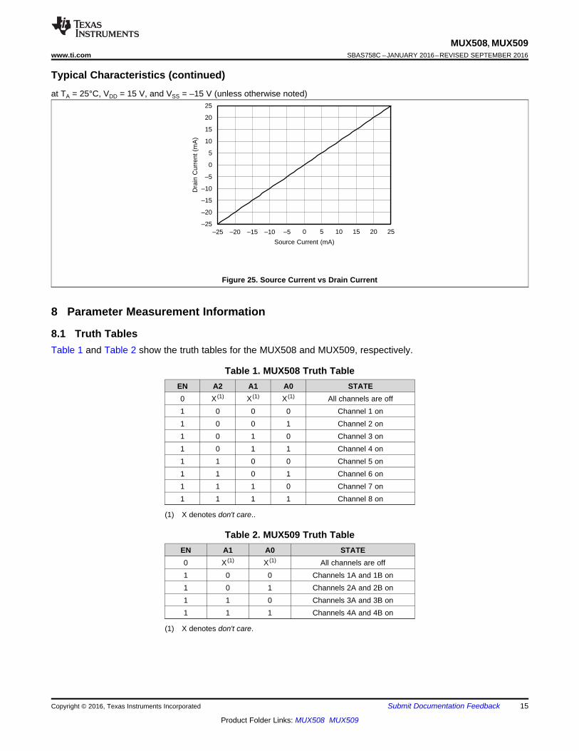
Typical Characteristics (continued)at TA = 25°C, VDD = 15 V, and VSS = –15 V (unless otherwise noted)
Figure 25. Source Current vs Drain Current
8 Parameter Measurement Information
8.1 Truth TablesTable 1 and Table 2 show the truth tables for the MUX508 and MUX509, respectively.
(1) X denotes don't care..
Table 1. MUX508 Truth TableEN A2 A1 A0 STATE0 X (1) X (1) X (1) All channels are off1 0 0 0 Channel 1 on1 0 0 1 Channel 2 on1 0 1 0 Channel 3 on1 0 1 1 Channel 4 on1 1 0 0 Channel 5 on1 1 0 1 Channel 6 on1 1 1 0 Channel 7 on1 1 1 1 Channel 8 on
(1) X denotes don't care.
Table 2. MUX509 Truth TableEN A1 A0 STATE0 X (1) X (1) All channels are off1 0 0 Channels 1A and 1B on1 0 1 Channels 2A and 2B on1 1 0 Channels 3A and 3B on1 1 1 Channels 4A and 4B on
D
VS VD
A A
ID (OFF)Is (OFF)
S
V
D
VS
ICH
S
16
MUX508, MUX509SBAS758C –JANUARY 2016–REVISED SEPTEMBER 2016 www.ti.com
Product Folder Links: MUX508 MUX509
Submit Documentation Feedback Copyright © 2016, Texas Instruments Incorporated
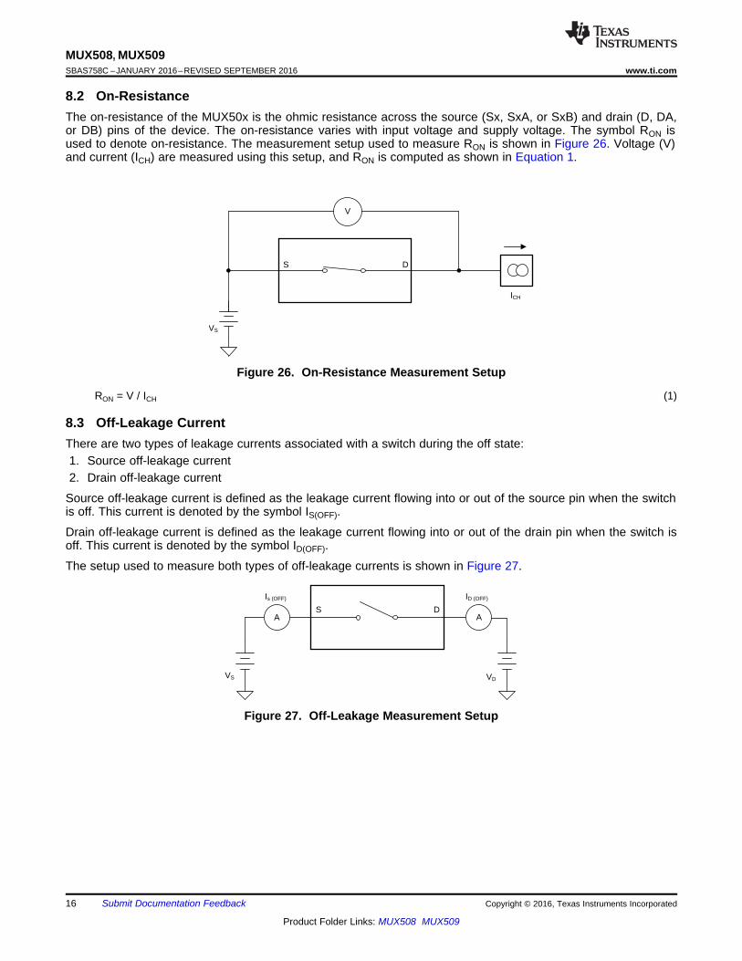
8.2 On-ResistanceThe on-resistance of the MUX50x is the ohmic resistance across the source (Sx, SxA, or SxB) and drain (D, DA,or DB) pins of the device. The on-resistance varies with input voltage and supply voltage. The symbol RON isused to denote on-resistance. The measurement setup used to measure RON is shown in Figure 26. Voltage (V)and current (ICH) are measured using this setup, and RON is computed as shown in Equation 1.
Figure 26. On-Resistance Measurement Setup
RON = V / ICH (1)
8.3 Off-Leakage CurrentThere are two types of leakage currents associated with a switch during the off state:1. Source off-leakage current2. Drain off-leakage current
Source off-leakage current is defined as the leakage current flowing into or out of the source pin when the switchis off. This current is denoted by the symbol IS(OFF).
Drain off-leakage current is defined as the leakage current flowing into or out of the drain pin when the switch isoff. This current is denoted by the symbol ID(OFF).
The setup used to measure both types of off-leakage currents is shown in Figure 27.
Figure 27. Off-Leakage Measurement Setup
50% 50%
tt
90%
90%
Output
Address Signal (VIN)
3 V
VIN
VDD
VDD
VSS
VSS
VS1
VS8
300 �� 35 pF
2 VMUX508
EN
A0
A1
A2
S1
S2-S7
S8
D
GND
VS8
VS1
Output
0 V
tt
Copyright © 2016, Texas Instruments Incorporated
D
VD
SA
ID (ON)
NC
NC = No Connection
17
MUX508, MUX509www.ti.com SBAS758C –JANUARY 2016–REVISED SEPTEMBER 2016
Product Folder Links: MUX508 MUX509
Submit Documentation FeedbackCopyright © 2016, Texas Instruments Incorporated
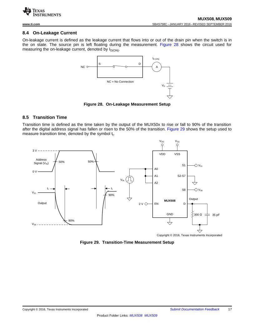
8.4 On-Leakage CurrentOn-leakage current is defined as the leakage current that flows into or out of the drain pin when the switch is inthe on state. The source pin is left floating during the measurement. Figure 28 shows the circuit used formeasuring the on-leakage current, denoted by ID(ON).
Figure 28. On-Leakage Measurement Setup
8.5 Transition TimeTransition time is defined as the time taken by the output of the MUX50x to rise or fall to 90% of the transitionafter the digital address signal has fallen or risen to the 50% of the transition. Figure 29 shows the setup used tomeasure transition time, denoted by the symbol tt.
Figure 29. Transition-Time Measurement Setup

VIN
VDD
VDD
VSS
VSS
VS
Output
300 �� 35 pF
2 V
MUX508
EN
A0
A1
A2
S1
S2-S7
S8
D
GND
3 V
Address Signal (VIN)
0 V
Output
tBBM
80% 80%
Copyright © 2016, Texas Instruments Incorporated
18
MUX508, MUX509SBAS758C –JANUARY 2016–REVISED SEPTEMBER 2016 www.ti.com
Product Folder Links: MUX508 MUX509
Submit Documentation Feedback Copyright © 2016, Texas Instruments Incorporated
8.6 Break-Before-Make DelayBreak-before-make delay is a safety feature that prevents two inputs from connecting when the MUX50x isswitching. The MUX50x output first breaks from the on-state switch before making the connection with the nexton-state switch. The time delay between the break and the make is known as a break-before-make delay.Figure 30 shows the setup used to measure break-before-make delay, denoted by the symbol tBBM.
Figure 30. Break-Before-Make Delay Measurement Setup

VDD
VDD
VSS
VSS
VS
Output
300 �� 35 pF
MUX508
EN
A0
A1
A2
S1
S2-S8
D
GND
VIN
3 V
Enable Drive (VIN)
0 V
50% 50%
tON (EN) tOFF (EN)
0.1 VS
0.9 VS
Output
Copyright © 2016, Texas Instruments Incorporated
19
MUX508, MUX509www.ti.com SBAS758C –JANUARY 2016–REVISED SEPTEMBER 2016
Product Folder Links: MUX508 MUX509
Submit Documentation FeedbackCopyright © 2016, Texas Instruments Incorporated
8.7 Turn-On and Turn-Off TimeTurn-on time is defined as the time taken by the output of the MUX50x to rise to a 90% final value after theenable signal has risen to a 50% final value. Figure 31 shows the setup used to measure turn-on time. Turn-ontime is denoted by the symbol tON.
Turn-off time is defined as the time taken by the output of the MUX50x to fall to a 10% initial value after theenable signal has fallen to a 50% initial value. Figure 31 shows the setup used to measure turn-off time. Turn-offtime is denoted by the symbol tOFF.
Figure 31. Turn-On and Turn-Off Time Measurement Setup

VDD VSS
MUX508
A0
A1
A2
VEN
RS
VS
EN
S
GND
CL
1 nF
DVOUT
VOUT
VEN
3 V
VOUT
QINJ = CL × VOUT
VDD VSS
Copyright © 2016, Texas Instruments Incorporated
0 V
20
MUX508, MUX509SBAS758C –JANUARY 2016–REVISED SEPTEMBER 2016 www.ti.com
Product Folder Links: MUX508 MUX509
Submit Documentation Feedback Copyright © 2016, Texas Instruments Incorporated
8.8 Charge InjectionThe MUX50x have a simple transmission-gate topology. Any mismatch in capacitance between the NMOS andPMOS transistors results in a charge injected into the drain or source during the falling or rising edge of the gatesignal. The amount of charge injected into the source or drain of the device is known as charge injection, and isdenoted by the symbol QINJ. Figure 32 shows the setup used to measure charge injection.
Figure 32. Charge-Injection Measurement Setup

OUT
S
VChannel-to-Channel Crosstalk 20 Log
V
§ · � ¨ ¸
© ¹
Network Analyzer
S1
S2
VS
VOUT
VDD
VDD
VSS
VSS
0.1 µF0.1 µF
RL
50 �
R50 �
GND
OUT
S
VOff Isolation 20 Log
V
§ · � ¨ ¸
© ¹
VDD VSS
Network Analyzer
VOUT
S
D
50 ��VS
VDD VSS
0.1 µF0.1 µF
GND
RL
50 �
50
21
MUX508, MUX509www.ti.com SBAS758C –JANUARY 2016–REVISED SEPTEMBER 2016
Product Folder Links: MUX508 MUX509
Submit Documentation FeedbackCopyright © 2016, Texas Instruments Incorporated
8.9 Off IsolationOff isolation is defined as the voltage at the drain pin (D, DA, or DB) of the MUX50x when a 1-VRMS signal isapplied to the source pin (Sx, SxA, or SxB) of an off-channel. Figure 33 shows the setup used to measure offisolation. Use Equation 2 to compute off isolation.
Figure 33. Off Isolation Measurement Setup
(2)
8.10 Channel-to-Channel CrosstalkChannel-to-channel crosstalk is defined as the voltage at the source pin (Sx, SxA, or SxB) of an off-channel,when a 1-VRMS signal is applied at the source pin of an on-channel. Figure 34 shows the setup used to measure,and Equation 3 is the equation used to compute, channel-to-channel crosstalk.
Figure 34. Channel-to-Channel Crosstalk Measurement Setup
(3)

VDD
VDD
VSS
VSS
GND
0.1 µF
Audio Precision
VOUT
S
D
VS
5 Vrms
RL
10 N�
IN
VIN
RS
0.1 µF
2
1
VAttenuation 20 Log
V
§ · � ¨ ¸
© ¹
Network Analyzer
VOUT
S
D
VS
V1
V2
VDD
VDD
VSS
VSS
0.1 µF0.1 µF
RL
50 �
50
GND
22
MUX508, MUX509SBAS758C –JANUARY 2016–REVISED SEPTEMBER 2016 www.ti.com
Product Folder Links: MUX508 MUX509
Submit Documentation Feedback Copyright © 2016, Texas Instruments Incorporated
8.11 BandwidthBandwidth is defined as the range of frequencies that are attenuated by < 3 dB when the input is applied to thesource pin of an on-channel and the output is measured at the drain pin of the MUX50x. Figure 35 shows thesetup used to measure bandwidth of the mux. Use Equation 4 to compute the attenuation.
Figure 35. Bandwidth Measurement Setup
(4)
8.12 THD + NoiseThe total harmonic distortion (THD) of a signal is defined as the ratio of the sum of the powers of all harmoniccomponents to the power of the fundamental frequency at the mux output. The on-resistance of the MUX50xvaries with the amplitude of the input signal and results in distortion when the drain pin is connected to a low-impedance load. Total harmonic distortion plus noise is denoted as THD+N. Figure 36 shows the setup used tomeasure the THD+N of the MUX50x.
Figure 36. THD+N Measurement Setup
S1
S2
S3
S8
A0 A1 A2
D
EN
1-of-8Decoder
MUX508
S4
S5
S6
S7
A0 A1
DB
EN
1-of-4Decoder
MUX509
S1A
S2A
S3A
S4B
S4A
S1B
S2B
S3B
DA
Copyright © 2016, Texas Instruments Incorporated
23
MUX508, MUX509www.ti.com SBAS758C –JANUARY 2016–REVISED SEPTEMBER 2016
Product Folder Links: MUX508 MUX509
Submit Documentation FeedbackCopyright © 2016, Texas Instruments Incorporated
9 Detailed Description
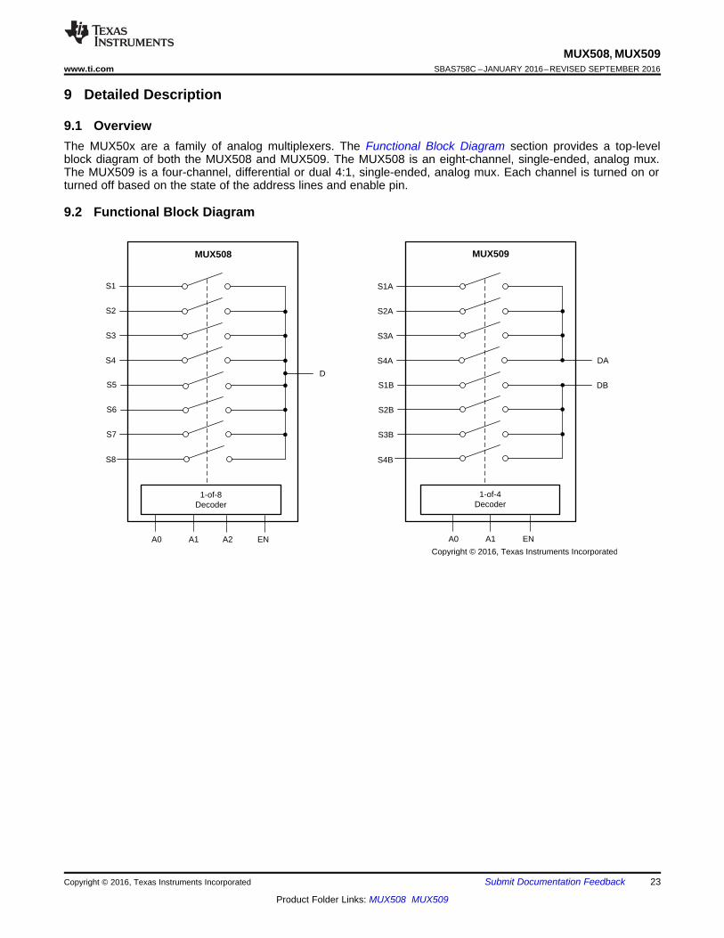
9.1 OverviewThe MUX50x are a family of analog multiplexers. The Functional Block Diagram section provides a top-levelblock diagram of both the MUX508 and MUX509. The MUX508 is an eight-channel, single-ended, analog mux.The MUX509 is a four-channel, differential or dual 4:1, single-ended, analog mux. Each channel is turned on orturned off based on the state of the address lines and enable pin.
9.2 Functional Block Diagram

S D
CGDP
CGDNCGSN
CGSP
OFF ON
OFF ON
±900
±600
±300
0
300
600
900
±75 ±50 ±25 0 25 50 75 100 125 150
Leak
age
Cur
rent
(pA
)
Temperature (�C) C006
ID(ON)+
ID(OFF)+
IS(OFF)+
IS(OFF)±
ID(OFF)±
ID(ON)±
24
MUX508, MUX509SBAS758C –JANUARY 2016–REVISED SEPTEMBER 2016 www.ti.com
Product Folder Links: MUX508 MUX509
Submit Documentation Feedback Copyright © 2016, Texas Instruments Incorporated
9.3 Feature Description
9.3.1 Ultralow Leakage CurrentThe MUX50x provide extremely low on- and off-leakage currents. The MUX50x are capable of switching signalsfrom high source-impedance inputs into a high input-impedance op amp with minimal offset error because ofthese ultralow leakage currents. Figure 37 shows typical leakage currents of the MUX50x versus temperature.
Figure 37. Leakage Current vs Temperature
9.3.2 Ultralow Charge InjectionThe MUX50x have a simple transmission gate topology, as shown in Figure 38. Any mismatch in the straycapacitance associated with the NMOS and PMOS transistors creates an output level change whenever theswitch is opened or closed.
Figure 38. Transmission Gate Topology
±9
±6
±3
0
3
6
9
±15 ±10 ±5 0 5 10 15
Cha
rge
Inje
ctio
n (p
C)
Drain voltage (V) C011
VDD = 12 V VSS = 0 V
VDD = 10 V VSS = ±10 V
VDD = 15 V VSS = ±15 V
±2
±1
0
1
2
±15 ±10 ±5 0 5 10 15
Cha
rge
Inje
ctio
n (p
C)
Source Voltage (V) C025
VDD = 12 V VSS = 0 V
VDD = 10 V VSS = ±10 V
VDD = 15 V VSS = ±15 V
25
MUX508, MUX509www.ti.com SBAS758C –JANUARY 2016–REVISED SEPTEMBER 2016
Product Folder Links: MUX508 MUX509
Submit Documentation FeedbackCopyright © 2016, Texas Instruments Incorporated
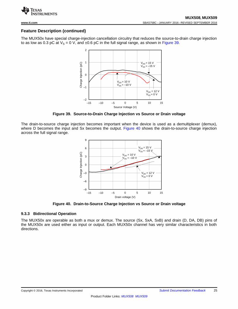
Feature Description (continued)The MUX50x have special charge-injection cancellation circuitry that reduces the source-to-drain charge injectionto as low as 0.3 pC at VS = 0 V, and ±0.6 pC in the full signal range, as shown in Figure 39.
Figure 39. Source-to-Drain Charge Injection vs Source or Drain voltage
The drain-to-source charge injection becomes important when the device is used as a demultiplexer (demux),where D becomes the input and Sx becomes the output. Figure 40 shows the drain-to-source charge injectionacross the full signal range.
Figure 40. Drain-to-Source Charge Injection vs Source or Drain voltage
9.3.3 Bidirectional OperationThe MUX50x are operable as both a mux or demux. The source (Sx, SxA, SxB) and drain (D, DA, DB) pins ofthe MUX50x are used either as input or output. Each MUX50x channel has very similar characteristics in bothdirections.

0
50
100
150
200
250
±20 ±15 ±10 ±5 0 5 10 15 20
On
Res
ista
nce
(�)
Source or Drain Voltage (V) C001
VDD = 15 V VSS = ±15 V
VDD = 18 V VSS = ±18 V
VDD = 16.5 V VSS = ±16.5 V
VDD = 13.5 V VSS = ±13.5 V
26
MUX508, MUX509SBAS758C –JANUARY 2016–REVISED SEPTEMBER 2016 www.ti.com
Product Folder Links: MUX508 MUX509
Submit Documentation Feedback Copyright © 2016, Texas Instruments Incorporated
Feature Description (continued)9.3.4 Rail-to-Rail OperationA valid analog signal for the MUX50x ranges from VSS to VDD. The input signal to the MUX50x can swing fromVSS to VDD without any significant degradation in performance. The on-resistance of the MUX50x varies withinput signal, as shown in Figure 41.
Figure 41. On-Resistance vs Source or Drain Voltage
9.4 Device Functional ModesWhen the EN pin of the MUX50x is pulled high, one of the switches is closed based on the state of the addresslines. When the EN pin is pulled low, all the switches are in an open state irrespective of the state of the addresslines. The EN pin can be connected to VDD (as high as 36 V).

ADS8864
REFVINP
VINM
+
+
+Charge
Kickback Filter
Gain Network
Gain Network
Gai
n N
etw
ork
Gain Network
High-Voltage Level Translation VCMHigh-Voltage Multiplexed Input
Reference Driver
REF3140 RC Filter OPA350 RC Filter
Analog Inputs
LEDPhoto
Detector
Bridge Sensor
Thermocouple
Current Sensing
Optical Sensor
OPA192
OPA192OPA140
MUX509
Copyright © 2016, Texas Instruments Incorporated
27
MUX508, MUX509www.ti.com SBAS758C –JANUARY 2016–REVISED SEPTEMBER 2016
Product Folder Links: MUX508 MUX509
Submit Documentation FeedbackCopyright © 2016, Texas Instruments Incorporated
10 Applications and Implementation
NOTEInformation in the following applications sections is not part of the TI componentspecification, and TI does not warrant its accuracy or completeness. TI’s customers areresponsible for determining suitability of components for their purposes. Customers shouldvalidate and test their design implementation to confirm system functionality.
10.1 Application InformationThe MUX50x family offers outstanding input/output leakage currents and ultralow charge injection. These devicesoperate up to 36 V, and offer true rail-to-rail input and output. The on-capacitance of the MUX50x is very low.These features makes the MUX50x a precision, robust, high-performance analog multiplexer for high-voltage,industrial applications.
10.2 Typical ApplicationFigure 42 shows a 16-bit, differential, four-channel, multiplexed, data-acquisition system. This example is typicalin industrial applications that require low distortion and a high-voltage differential input. The circuit uses theADS8864, a 16-bit, 400-kSPS successive-approximation-resistor (SAR) analog-to-digital converter (ADC), alongwith a precision, high-voltage, signal-conditioning front end, and a four-channel differential mux. This applicationexample details the process for optimizing a precision, high-voltage, front-end drive circuit using the MUX509,OPA192 and OPA140 to achieve excellent dynamic performance and linearity with the ADS8864.
Figure 42. 16-Bit Precision Multiplexed Data-Acquisition System for High-Voltage Inputs With LowestDistortion
10.2.1 Design RequirementsThe primary objective is to design a ±20 V, differential, four-channel, multiplexed, data-acquisition system withlowest distortion using the 16-bit ADS8864 at a throughput of 400 kSPS for a 10-kHz, full-scale, pure, sine-waveinput. The design requirements for this block design are:
• System supply voltage: ±15 V• ADC supply voltage: 3.3 V• ADC sampling rate: 400 kSPS• ADC reference voltage (REFP): 4.096 V• System input signal: A high-voltage differential input signal with a peak amplitude of 20 V and frequency
(fIN) of 10 kHz are applied to each differential input of the mux.

±1.0
±0.8
±0.6
±0.4
±0.2
0.0
0.2
0.4
0.6
0.8
1.0
±20 ±15 ±10 ±5 0 5 10 15 20
Inte
gral
Non
-Lin
earit
y (L
SB
)
ADC Differential Peak-to-Peak Input (V) C030
28
MUX508, MUX509SBAS758C –JANUARY 2016–REVISED SEPTEMBER 2016 www.ti.com
Product Folder Links: MUX508 MUX509
Submit Documentation Feedback Copyright © 2016, Texas Instruments Incorporated
Typical Application (continued)10.2.2 Detailed Design ProcedureThe purpose of this precision design is to design an optimal, high-voltage, multiplexed, data-acquisition systemfor highest system linearity and fast settling. The overall system block diagram is illustrated in Figure 42. Thecircuit is a multichannel, data-acquisition signal chain consisting of an input low-pass filter, mux, mux outputbuffer, attenuating SAR ADC driver, and the reference driver. The architecture allows fast sampling of multiplechannels using a single ADC, providing a low-cost solution. This design systematically approaches each analogcircuit block to achieve a 16-bit settling for a full-scale input stage voltage and linearity for a 10-kHz sinusoidalinput signal at each input channel.
For step-by-step design procedure, circuit schematics, bill of materials, PCB files, simulation results, and testresults, see TI Precision Design TIPD151, 16-Bit, 400-kSPS, 4-Channel Multiplexed Data-Acquisition Systemfor High-Voltage Inputs with Lowest Distortion.
10.2.3 Application Curve
Figure 43. ADC 16-Bit Linearity Error for the Multiplexed Data-Acquisition Block

0
50
100
150
200
250
±20 ±15 ±10 ±5 0 5 10 15 20
On
Res
ista
nce
(�)
Source or Drain Voltage (V) C001
VDD = 15 V VSS = ±15 V
VDD = 18 V VSS = ±18 V
VDD = 16.5 V VSS = ±16.5 V
VDD = 13.5 V VSS = ±13.5 V
29
MUX508, MUX509www.ti.com SBAS758C –JANUARY 2016–REVISED SEPTEMBER 2016
Product Folder Links: MUX508 MUX509
Submit Documentation FeedbackCopyright © 2016, Texas Instruments Incorporated
11 Power-Supply RecommendationsThe MUX50x operates across a wide supply range of ±5 V to ±18 V (10 V to 36 V in single-supply mode). TheMUX508 and MUX509 operate equally well with either dual supplies (±5 V to ±18 V), or a single supply (10 V to36 V). They also perform well with unsymmetric supplies such as VDD = 12 V and VSS = –5 V. For reliableoperation, use a supply decoupling capacitor with a capacitance between 0.1 µF to 10 µF at both the VDD andVSS pins to ground.
The on-resistance of the MUX50x varies with supply voltage, as shown in Figure 44.
Figure 44. On-Resistance Variation With Supply and Input Voltage

DB
AO EN
A1
AO
EN
VSS
S1A
S2A
S3A
DA
A1
GND
VDD
S1B
S2B
S3B
S4BS4A
Via to ground plane
Via to ground plane
MUX509IPW
C C
Copyright © 2016, Texas Instruments Incorporated
AO EN A2
A1
AO
EN
VSS
S1
S2
S3
D
A1
A2
GND
VDD
S5
S6
S7
S8
S4
Via to ground plane
Via to ground plane
MUX508IPW
C
C
Copyright © 2016, Texas Instruments Incorporated
30
MUX508, MUX509SBAS758C –JANUARY 2016–REVISED SEPTEMBER 2016 www.ti.com
Product Folder Links: MUX508 MUX509
Submit Documentation Feedback Copyright © 2016, Texas Instruments Incorporated
12 Layout
12.1 Layout GuidelinesFigure 45 shows an example of a PCB layout with the MUX508IPW, and Figure 46 shows an example of a PCBlayout with MUX509IPW. The guidelines provided in this section are also applicable to the SOIC MUX508ID andMUX509ID package variants as well.
Some key considerations are:1. Decouple the VDD and VSS pins with a 0.1-µF capacitor, placed as close to the pin as possible. Make sure
that the capacitor voltage rating is sufficient for the VDD and VSS supplies.2. Keep the input lines as small as possible. For the MUX509 differential signals, make sure the A inputs and B
inputs are as symmetric as possible.3. Use a solid ground plane to help distribute heat and reduce electromagnetic interference (EMI) noise pickup.4. Do not run sensitive analog traces in parallel with digital traces. Avoid crossing digital and analog traces if
possible and only make perpendicular crossings when necessary.
12.2 Layout Example
Figure 45. MUX508IPW Layout Example
Figure 46. MUX509IPW Layout Example
31
MUX508, MUX509www.ti.com SBAS758C –JANUARY 2016–REVISED SEPTEMBER 2016
Product Folder Links: MUX508 MUX509
Submit Documentation FeedbackCopyright © 2016, Texas Instruments Incorporated
13 Device and Documentation Support
13.1 Documentation Support
13.1.1 Related Documentation• ADS866x 12-Bit, 500-kSPS, 4- and 8-Channel, Single-Supply, SAR ADCs with Bipolar Input Ranges
(SBAS492)• OPAx140 High-Precision, Low-Noise, Rail-to-Rail Output, 11-MHz JFET Op Amp (SBOS498)• OPAx192 36-V, Precision, Rail-to-Rail Input/Output, Low Offset Voltage, Low Input Bias Current Op Amp with
e-trim™ (SBOS620)
13.2 Related LinksTable 3 lists quick access links. Categories include technical documents, support and community resources,tools and software, and quick access to sample or buy.
Table 3. Related Links
PARTS PRODUCT FOLDER SAMPLE & BUY TECHNICALDOCUMENTS
TOOLS &SOFTWARE
SUPPORT &COMMUNITY
MUX508 Click here Click here Click here Click here Click hereMUX509 Click here Click here Click here Click here Click here
13.3 Receiving Notification of Documentation UpdatesTo receive notification of documentation updates, navigate to the device product folder on ti.com. In the upperright corner, click on Alert me to register and receive a weekly digest of any product information that haschanged. For change details, review the revision history included in any revised document.
13.4 Community ResourcesThe following links connect to TI community resources. Linked contents are provided "AS IS" by the respectivecontributors. They do not constitute TI specifications and do not necessarily reflect TI's views; see TI's Terms ofUse.
TI E2E™ Online Community TI's Engineer-to-Engineer (E2E) Community. Created to foster collaborationamong engineers. At e2e.ti.com, you can ask questions, share knowledge, explore ideas and helpsolve problems with fellow engineers.
Design Support TI's Design Support Quickly find helpful E2E forums along with design support tools andcontact information for technical support.
13.5 TrademarksE2E is a trademark of Texas Instruments.All other trademarks are the property of their respective owners.
13.6 Electrostatic Discharge CautionThis integrated circuit can be damaged by ESD. Texas Instruments recommends that all integrated circuits be handled withappropriate precautions. Failure to observe proper handling and installation procedures can cause damage.
ESD damage can range from subtle performance degradation to complete device failure. Precision integrated circuits may be moresusceptible to damage because very small parametric changes could cause the device not to meet its published specifications.
13.7 GlossarySLYZ022 — TI Glossary.
This glossary lists and explains terms, acronyms, and definitions.
32
MUX508, MUX509SBAS758C –JANUARY 2016–REVISED SEPTEMBER 2016 www.ti.com
Product Folder Links: MUX508 MUX509
Submit Documentation Feedback Copyright © 2016, Texas Instruments Incorporated
14 Mechanical, Packaging, and Orderable InformationThe following pages include mechanical packaging and orderable information. This information is the mostcurrent data available for the designated devices. This data is subject to change without notice and revision ofthis document. For browser-based versions of this data sheet, refer to the left-hand navigation.

PACKAGE OPTION ADDENDUM
www.ti.com 18-Jan-2018
Addendum-Page 1
PACKAGING INFORMATION
Orderable Device Status(1)
Package Type PackageDrawing
Pins PackageQty
Eco Plan(2)
Lead/Ball Finish(6)
MSL Peak Temp(3)
Op Temp (°C) Device Marking(4/5)
Samples
MUX508ID ACTIVE SOIC D 16 40 Green (RoHS& no Sb/Br)
CU SN Level-2-260C-1 YEAR -40 to 125 M36508D
MUX508IDR ACTIVE SOIC D 16 2500 Green (RoHS& no Sb/Br)
CU SN Level-2-260C-1 YEAR -40 to 125 M36508D
MUX508IPW ACTIVE TSSOP PW 16 90 Green (RoHS& no Sb/Br)
CU NIPDAU Level-2-260C-1 YEAR -40 to 125 MUX508B
MUX508IPWR ACTIVE TSSOP PW 16 2000 Green (RoHS& no Sb/Br)
CU NIPDAU Level-2-260C-1 YEAR -40 to 125 MUX508B
MUX509ID ACTIVE SOIC D 16 40 Green (RoHS& no Sb/Br)
CU SN Level-2-260C-1 YEAR -40 to 125 M36509D
MUX509IDR ACTIVE SOIC D 16 2500 Green (RoHS& no Sb/Br)
CU SN Level-2-260C-1 YEAR -40 to 125 M36509D
MUX509IPW ACTIVE TSSOP PW 16 90 Green (RoHS& no Sb/Br)
CU NIPDAU Level-2-260C-1 YEAR -40 to 125 MUX509C
MUX509IPWR ACTIVE TSSOP PW 16 2000 Green (RoHS& no Sb/Br)
CU NIPDAU Level-2-260C-1 YEAR -40 to 125 MUX509C
(1) The marketing status values are defined as follows:ACTIVE: Product device recommended for new designs.LIFEBUY: TI has announced that the device will be discontinued, and a lifetime-buy period is in effect.NRND: Not recommended for new designs. Device is in production to support existing customers, but TI does not recommend using this part in a new design.PREVIEW: Device has been announced but is not in production. Samples may or may not be available.OBSOLETE: TI has discontinued the production of the device.
(2) RoHS: TI defines "RoHS" to mean semiconductor products that are compliant with the current EU RoHS requirements for all 10 RoHS substances, including the requirement that RoHS substancedo not exceed 0.1% by weight in homogeneous materials. Where designed to be soldered at high temperatures, "RoHS" products are suitable for use in specified lead-free processes. TI mayreference these types of products as "Pb-Free".RoHS Exempt: TI defines "RoHS Exempt" to mean products that contain lead but are compliant with EU RoHS pursuant to a specific EU RoHS exemption.Green: TI defines "Green" to mean the content of Chlorine (Cl) and Bromine (Br) based flame retardants meet JS709B low halogen requirements of <=1000ppm threshold. Antimony trioxide basedflame retardants must also meet the <=1000ppm threshold requirement.
(3) MSL, Peak Temp. - The Moisture Sensitivity Level rating according to the JEDEC industry standard classifications, and peak solder temperature.
(4) There may be additional marking, which relates to the logo, the lot trace code information, or the environmental category on the device.

PACKAGE OPTION ADDENDUM
www.ti.com 18-Jan-2018
Addendum-Page 2
(5) Multiple Device Markings will be inside parentheses. Only one Device Marking contained in parentheses and separated by a "~" will appear on a device. If a line is indented then it is a continuationof the previous line and the two combined represent the entire Device Marking for that device.
(6) Lead/Ball Finish - Orderable Devices may have multiple material finish options. Finish options are separated by a vertical ruled line. Lead/Ball Finish values may wrap to two lines if the finishvalue exceeds the maximum column width.
Important Information and Disclaimer:The information provided on this page represents TI's knowledge and belief as of the date that it is provided. TI bases its knowledge and belief on informationprovided by third parties, and makes no representation or warranty as to the accuracy of such information. Efforts are underway to better integrate information from third parties. TI has taken andcontinues to take reasonable steps to provide representative and accurate information but may not have conducted destructive testing or chemical analysis on incoming materials and chemicals.TI and TI suppliers consider certain information to be proprietary, and thus CAS numbers and other limited information may not be available for release.
In no event shall TI's liability arising out of such information exceed the total purchase price of the TI part(s) at issue in this document sold by TI to Customer on an annual basis.

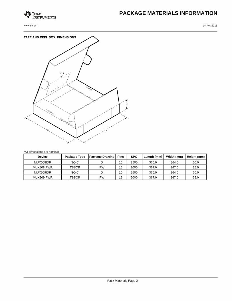
TAPE AND REEL INFORMATION
*All dimensions are nominal
Device PackageType
PackageDrawing
Pins SPQ ReelDiameter
(mm)
ReelWidth
W1 (mm)
A0(mm)
B0(mm)
K0(mm)
P1(mm)
W(mm)
Pin1Quadrant
MUX508IDR SOIC D 16 2500 330.0 16.8 6.5 10.3 2.1 8.0 16.0 Q1
MUX508IPWR TSSOP PW 16 2000 330.0 12.4 6.9 5.6 1.6 8.0 12.0 Q1
MUX509IDR SOIC D 16 2500 330.0 16.8 6.5 10.3 2.1 8.0 16.0 Q1
MUX509IPWR TSSOP PW 16 2000 330.0 12.4 6.9 5.6 1.6 8.0 12.0 Q1
PACKAGE MATERIALS INFORMATION
www.ti.com 14-Jan-2018
Pack Materials-Page 1
*All dimensions are nominal
Device Package Type Package Drawing Pins SPQ Length (mm) Width (mm) Height (mm)
MUX508IDR SOIC D 16 2500 366.0 364.0 50.0
MUX508IPWR TSSOP PW 16 2000 367.0 367.0 35.0
MUX509IDR SOIC D 16 2500 366.0 364.0 50.0
MUX509IPWR TSSOP PW 16 2000 367.0 367.0 35.0
PACKAGE MATERIALS INFORMATION
www.ti.com 14-Jan-2018
Pack Materials-Page 2


IMPORTANT NOTICE
Texas Instruments Incorporated (TI) reserves the right to make corrections, enhancements, improvements and other changes to itssemiconductor products and services per JESD46, latest issue, and to discontinue any product or service per JESD48, latest issue. Buyersshould obtain the latest relevant information before placing orders and should verify that such information is current and complete.TI’s published terms of sale for semiconductor products (http://www.ti.com/sc/docs/stdterms.htm) apply to the sale of packaged integratedcircuit products that TI has qualified and released to market. Additional terms may apply to the use or sale of other types of TI products andservices.Reproduction of significant portions of TI information in TI data sheets is permissible only if reproduction is without alteration and isaccompanied by all associated warranties, conditions, limitations, and notices. TI is not responsible or liable for such reproduceddocumentation. Information of third parties may be subject to additional restrictions. Resale of TI products or services with statementsdifferent from or beyond the parameters stated by TI for that product or service voids all express and any implied warranties for theassociated TI product or service and is an unfair and deceptive business practice. TI is not responsible or liable for any such statements.Buyers and others who are developing systems that incorporate TI products (collectively, “Designers”) understand and agree that Designersremain responsible for using their independent analysis, evaluation and judgment in designing their applications and that Designers havefull and exclusive responsibility to assure the safety of Designers' applications and compliance of their applications (and of all TI productsused in or for Designers’ applications) with all applicable regulations, laws and other applicable requirements. Designer represents that, withrespect to their applications, Designer has all the necessary expertise to create and implement safeguards that (1) anticipate dangerousconsequences of failures, (2) monitor failures and their consequences, and (3) lessen the likelihood of failures that might cause harm andtake appropriate actions. Designer agrees that prior to using or distributing any applications that include TI products, Designer willthoroughly test such applications and the functionality of such TI products as used in such applications.TI’s provision of technical, application or other design advice, quality characterization, reliability data or other services or information,including, but not limited to, reference designs and materials relating to evaluation modules, (collectively, “TI Resources”) are intended toassist designers who are developing applications that incorporate TI products; by downloading, accessing or using TI Resources in anyway, Designer (individually or, if Designer is acting on behalf of a company, Designer’s company) agrees to use any particular TI Resourcesolely for this purpose and subject to the terms of this Notice.TI’s provision of TI Resources does not expand or otherwise alter TI’s applicable published warranties or warranty disclaimers for TIproducts, and no additional obligations or liabilities arise from TI providing such TI Resources. TI reserves the right to make corrections,enhancements, improvements and other changes to its TI Resources. TI has not conducted any testing other than that specificallydescribed in the published documentation for a particular TI Resource.Designer is authorized to use, copy and modify any individual TI Resource only in connection with the development of applications thatinclude the TI product(s) identified in such TI Resource. NO OTHER LICENSE, EXPRESS OR IMPLIED, BY ESTOPPEL OR OTHERWISETO ANY OTHER TI INTELLECTUAL PROPERTY RIGHT, AND NO LICENSE TO ANY TECHNOLOGY OR INTELLECTUAL PROPERTYRIGHT OF TI OR ANY THIRD PARTY IS GRANTED HEREIN, including but not limited to any patent right, copyright, mask work right, orother intellectual property right relating to any combination, machine, or process in which TI products or services are used. Informationregarding or referencing third-party products or services does not constitute a license to use such products or services, or a warranty orendorsement thereof. Use of TI Resources may require a license from a third party under the patents or other intellectual property of thethird party, or a license from TI under the patents or other intellectual property of TI.TI RESOURCES ARE PROVIDED “AS IS” AND WITH ALL FAULTS. TI DISCLAIMS ALL OTHER WARRANTIES ORREPRESENTATIONS, EXPRESS OR IMPLIED, REGARDING RESOURCES OR USE THEREOF, INCLUDING BUT NOT LIMITED TOACCURACY OR COMPLETENESS, TITLE, ANY EPIDEMIC FAILURE WARRANTY AND ANY IMPLIED WARRANTIES OFMERCHANTABILITY, FITNESS FOR A PARTICULAR PURPOSE, AND NON-INFRINGEMENT OF ANY THIRD PARTY INTELLECTUALPROPERTY RIGHTS. TI SHALL NOT BE LIABLE FOR AND SHALL NOT DEFEND OR INDEMNIFY DESIGNER AGAINST ANY CLAIM,INCLUDING BUT NOT LIMITED TO ANY INFRINGEMENT CLAIM THAT RELATES TO OR IS BASED ON ANY COMBINATION OFPRODUCTS EVEN IF DESCRIBED IN TI RESOURCES OR OTHERWISE. IN NO EVENT SHALL TI BE LIABLE FOR ANY ACTUAL,DIRECT, SPECIAL, COLLATERAL, INDIRECT, PUNITIVE, INCIDENTAL, CONSEQUENTIAL OR EXEMPLARY DAMAGES INCONNECTION WITH OR ARISING OUT OF TI RESOURCES OR USE THEREOF, AND REGARDLESS OF WHETHER TI HAS BEENADVISED OF THE POSSIBILITY OF SUCH DAMAGES.Unless TI has explicitly designated an individual product as meeting the requirements of a particular industry standard (e.g., ISO/TS 16949and ISO 26262), TI is not responsible for any failure to meet such industry standard requirements.Where TI specifically promotes products as facilitating functional safety or as compliant with industry functional safety standards, suchproducts are intended to help enable customers to design and create their own applications that meet applicable functional safety standardsand requirements. Using products in an application does not by itself establish any safety features in the application. Designers mustensure compliance with safety-related requirements and standards applicable to their applications. Designer may not use any TI products inlife-critical medical equipment unless authorized officers of the parties have executed a special contract specifically governing such use.Life-critical medical equipment is medical equipment where failure of such equipment would cause serious bodily injury or death (e.g., lifesupport, pacemakers, defibrillators, heart pumps, neurostimulators, and implantables). Such equipment includes, without limitation, allmedical devices identified by the U.S. Food and Drug Administration as Class III devices and equivalent classifications outside the U.S.TI may expressly designate certain products as completing a particular qualification (e.g., Q100, Military Grade, or Enhanced Product).Designers agree that it has the necessary expertise to select the product with the appropriate qualification designation for their applicationsand that proper product selection is at Designers’ own risk. Designers are solely responsible for compliance with all legal and regulatoryrequirements in connection with such selection.Designer will fully indemnify TI and its representatives against any damages, costs, losses, and/or liabilities arising out of Designer’s non-compliance with the terms and provisions of this Notice.
Mailing Address: Texas Instruments, Post Office Box 655303, Dallas, Texas 75265Copyright © 2018, Texas Instruments Incorporated