33883 H-Bridge Gate Driver ICpdf-file.ic37.com/pdf1/MOTOROLA/MC33883_datasheet... · H-Bridge Gate...
20
MOTOROLA SEMICONDUCTOR TECHNICAL DATA © Motorola, Inc. 2004 33883 Simplified Application Diagram Document order number: MC33883/D Rev 6.0, 01/2004 33883 Simplified Application Diagram MCU 33883 V BOOST V BAT GND SRC_HS2 GATE_LS2 CP_OUT LR_OUT GATE_HS1 SRC_HS1 GATE_LS1 GATE_HS2 IN_HS1 IN_LS1 IN_HS2 IN_LS2 V CC V CC 2 G_EN C1 C2 DC Motor H-Bridge Gate Driver IC The 33883 is an H-bridge gate driver (also known as a full-bridge predriver) IC with integrated charge pump and independent high- and low-side gate driver channels. The gate driver channels are independently controlled by four separate input terminals, thus allowing the device to be optionally configured as two independent high-side gate drivers and two independent low-side gate drivers. The low-side channels are referenced to ground. The high-side channels are floating. The gate driver outputs can source and sink up to 1.0 A peak current pulses, permitting large gate-charge MOSFETs to be driven and/or high Pulse Width Modulation (PWM) frequencies to be utilized. A linear regulator is incorporated, providing a 15 V typical gate supply to the low-side gate drivers. Features • V CC Operating Voltage Range from 5.5 V up to 55 V • V CC2 Operating Voltage Range from 5.5 V up to 28 V • CMOS/LSTTL Compatible I/O • 1.0 A Peak Gate Driver Current • Built-In High-Side Charge Pump • Undervoltage Lockout (UVLO) • Overvoltage Lockout (OVLO) • Global Enable with <10 µA Sleep Mode • Supports PWM up to 100 kHz ORDERING INFORMATION Device Temperature Range (T A ) Package MC33883DW/R2 -40°C to 125°C 20 SOICW DW SUFFIX CASE 751D-06 20-TERMINAL SOICW H-BRIDGE GATE DRIVER IC Freescale Semiconductor, I Freescale Semiconductor, Inc. For More Information On This Product, Go to: www.freescale.com nc...
Transcript of 33883 H-Bridge Gate Driver ICpdf-file.ic37.com/pdf1/MOTOROLA/MC33883_datasheet... · H-Bridge Gate...
MOTOROLASEMICONDUCTOR TECHNICAL DATA
© Motorola, Inc. 2004
33883 Simplified Application Diagram
Document order number: MC33883/DRev 6.0, 01/2004
33883
Simplified Application Diagram
MCU
33883
VBOOSTVBAT
GND
SRC_HS2
GATE_LS2
CP_OUT
LR_OUT
GATE_HS1
SRC_HS1
GATE_LS1
GATE_HS2
IN_HS1IN_LS1IN_HS2IN_LS2
VCCVCC2G_EN
C1C2
DCMotor
H-Bridge Gate Driver ICThe 33883 is an H-bridge gate driver (also known as a full-bridge predriver)
IC with integrated charge pump and independent high- and low-side gate driver channels. The gate driver channels are independently controlled by four separate input terminals, thus allowing the device to be optionally configured as two independent high-side gate drivers and two independent low-side gate drivers. The low-side channels are referenced to ground. The high-side channels are floating.
The gate driver outputs can source and sink up to 1.0 A peak current pulses, permitting large gate-charge MOSFETs to be driven and/or high Pulse Width Modulation (PWM) frequencies to be utilized. A linear regulator is incorporated, providing a 15 V typical gate supply to the low-side gate drivers.
Features• VCC Operating Voltage Range from 5.5 V up to 55 V• VCC2 Operating Voltage Range from 5.5 V up to 28 V• CMOS/LSTTL Compatible I/O• 1.0 A Peak Gate Driver Current • Built-In High-Side Charge Pump • Undervoltage Lockout (UVLO)• Overvoltage Lockout (OVLO)• Global Enable with <10 µA Sleep Mode• Supports PWM up to 100 kHz
ORDERING INFORMATION
DeviceTemperature Range (TA) Package
MC33883DW/R2 -40°C to 125°C 20 SOICW
DW SUFFIXCASE 751D-06
20-TERMINAL SOICW
H-BRIDGE GATE DRIVER IC
Fre
esc
ale
Se
mic
on
du
cto
r, I
Freescale Semiconductor, Inc.
For More Information On This Product, Go to: www.freescale.com
nc
...

33883 MOTOROLA ANALOG INTEGRATED CIRCUIT DEVICE DATA2
Figure 1. 33883 Simplified Internal Block Diagram
Undervoltage/Overvoltage
Detection
G_EN
IN_HS1
IN_LS1
IN_HS2
IN_LS2
GATE_LS1
SRC_HS1
GATE_HS1
CP_OUT
LR_OUT
GATE_LS2
SRC_HS2
GATE_HS2
5.5 V –55 V
5.5 V– 28 V
PulseGenerator
VDD/VCC Level Shift
Pulse Generator
VDD/VPOS Level Shift
IN OUT
Control and
Logic
LinearReg
VCC2
ENGND
+5.0 V
+14.5 V
VDD
HIGH- AND LOW-SIDE
ChargePump
EN
GND
C2
VPOS
VCC C1
VCC2
VCC
VCC
VCC2
VCC
VCC2
CP_OUT
LR_OUT
VCC, VCC2
VDD
C2C1
BRG_EN
Pulse Generator
VDD/VCC Level Shift
Pulse Generator
VDD/VPOS Level Shift
GND1
CONTROL WITH CHARGE PUMP
CCP_OUT
CLR_OUT
CCP
CP_OUTVCC
OutputDriver
IN OUT
CP_OUTVCC
OutputDriver
IN OUT
LR_OUT
OutputDriver
IN OUT
LR_OUT
OutputDriver
Control and
Logic
Control and
Logic
Control and
Logic
BRG_EN
BRG_EN
BRG_ENHIGH-SIDE CHANNEL
LOW-SIDE CHANNEL
HIGH-SIDE CHANNEL
LOW-SIDE CHANNEL
GND2
GND2
GND1
GND2 GND_A
GND2GND_A
TSD1Thermal Shutdown
TSD1
TSD1
TSD2Thermal Shutdown
TSD2
TSD2
Fre
esc
ale
Se
mic
on
du
cto
r, I
Freescale Semiconductor, Inc.
For More Information On This Product, Go to: www.freescale.com
nc
...
MOTOROLA ANALOG INTEGRATED CIRCUIT DEVICE DATA 338833
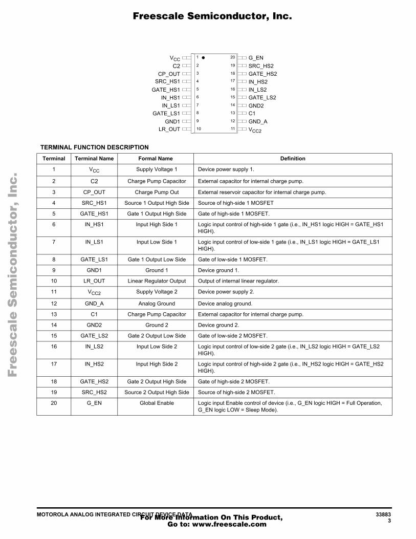
TERMINAL FUNCTION DESCRIPTION
Terminal Terminal Name Formal Name Definition
1 VCC Supply Voltage 1 Device power supply 1.
2 C2 Charge Pump Capacitor External capacitor for internal charge pump.
3 CP_OUT Charge Pump Out External reservoir capacitor for internal charge pump.
4 SRC_HS1 Source 1 Output High Side Source of high-side 1 MOSFET
5 GATE_HS1 Gate 1 Output High Side Gate of high-side 1 MOSFET.
6 IN_HS1 Input High Side 1 Logic input control of high-side 1 gate (i.e., IN_HS1 logic HIGH = GATE_HS1 HIGH).
7 IN_LS1 Input Low Side 1 Logic input control of low-side 1 gate (i.e., IN_LS1 logic HIGH = GATE_LS1 HIGH).
8 GATE_LS1 Gate 1 Output Low Side Gate of low-side 1 MOSFET.
9 GND1 Ground 1 Device ground 1.
10 LR_OUT Linear Regulator Output Output of internal linear regulator.
11 VCC2 Supply Voltage 2 Device power supply 2.
12 GND_A Analog Ground Device analog ground.
13 C1 Charge Pump Capacitor External capacitor for internal charge pump.
14 GND2 Ground 2 Device ground 2.
15 GATE_LS2 Gate 2 Output Low Side Gate of low-side 2 MOSFET.
16 IN_LS2 Input Low Side 2 Logic input control of low-side 2 gate (i.e., IN_LS2 logic HIGH = GATE_LS2 HIGH).
17 IN_HS2 Input High Side 2 Logic input control of high-side 2 gate (i.e., IN_HS2 logic HIGH = GATE_HS2 HIGH).
18 GATE_HS2 Gate 2 Output High Side Gate of high-side 2 MOSFET.
19 SRC_HS2 Source 2 Output High Side Source of high-side 2 MOSFET.
20 G_EN Global Enable Logic input Enable control of device (i.e., G_EN logic HIGH = Full Operation, G_EN logic LOW = Sleep Mode).
VCC
CP_OUT
IN_LS1GATE_LS1
GND1LR_OUT
SRC_HS1GATE_HS1
IN_HS1
C2G_EN
IN_HS2IN_LS2GATE_LS2GND2C1GND_AVCC2
SRC_HS2GATE_HS2
4
5
6
7
8
9
10
2
3
20
18
14
13
12
11
17
16
15
19
1
Fre
esc
ale
Se
mic
on
du
cto
r, I
Freescale Semiconductor, Inc.
For More Information On This Product, Go to: www.freescale.com
nc
...

33883 MOTOROLA ANALOG INTEGRATED CIRCUIT DEVICE DATA4
MAXIMUM RATINGS All voltages are with respect to ground unless otherwise noted.
Rating Symbol Value Unit
Supply Voltage 1 VCC -0.3 to 65 V
Supply Voltage 2 (Note 1) VCC2 -0.3 to 35 V
Linear Regulator Output Voltage VLR_OUT -0.3 to 18 V
High-Side Floating Supply Absolute Voltage VCP_OUT -0.3 to 65 V
High-Side Floating Source Voltage VSRC_HS -1.0 to 65 V
High-Side Source Current from CP_OUT in Switch ON State IS 250 mA
High-Side Gate Voltage VGATE_HS -0.3 to 65 V
High-Side Gate Source Voltage VGATE_HS - VSRC_HS -0.3 to 20 V
High-Side Floating Supply Gate Voltage VCP_OUT - VGATE_HS -0.3 to 65 V
Low-Side Gate Voltage VGATE_LS -0.3 to 17 V
Wake-Up Voltage VG_EN -0.3 to 35 V
Logic Input Voltage VIN -0.3 to 10 V
Charge Pump Capacitor Voltage VC1 -0.3 to VLR_OUT V
Charge Pump Capacitor Voltage VC2 -0.3 to 65 V
ESD VoltageHuman Body Model on All Pins (VCC and VCC2 as Two Power Supplies) (Note 2)Machine Model (Note 3)
VESD1
VESD2
±1500±130
V
Power Dissipation and Thermal CharacteristicsMaximum Power Dissipation @ 25°CThermal Resistance (Junction to Ambient)Operating Junction TemperatureStorage Temperature
PDRθJA
TJTSTG
1.25100
-40 to 150-65 to 150
W°C/W
°C°C
Terminal Soldering Temperature (Note 4) TSOLDER 240 °C
Notes1. VCC2 can sustain load dump pulse of 40 V, 400 ms, 2.0 Ω.2. ESD1 testing is performed in accordance with the Human Body Model (CZAP=100 pF, RZAP=1500 Ω).3. ESD2 testing is performed in accordance with the Machine Model (CZAP=200 pF, RZAP=0 Ω).4. Terminal soldering temperature limit is for 10 second maximum duration. Not designed for immersion soldering. Exceeding these limits may
cause malfunction or permanent damage to the device.
Fre
esc
ale
Se
mic
on
du
cto
r, I
Freescale Semiconductor, Inc.
For More Information On This Product, Go to: www.freescale.com
nc
...

MOTOROLA ANALOG INTEGRATED CIRCUIT DEVICE DATA 338835
STATIC ELECTRICAL CHARACTERISTICSCharacteristics noted under conditions VCC = 12 V, VCC2 = 12 V, CCP = 33 nF, G_EN = 4.5 V unless otherwise noted. Typical values for TA = 25°C and min/max values for TA = -40°C to 125°C unless otherwise noted.
Characteristic Symbol Min Typ Max Unit
OPERATING CONDITIONS
Supply Voltage 1 for Output High-Side Driver and Charge Pump VCC 5.5 – 55 V
Supply Voltage 2 for Linear Regulation VCC2 5.5 – 28 V
High-Side Floating Supply Absolute Voltage VCP_OUT VCC+4 – VCC+11 but < 65
V
LOGIC
Logic 1 Input Voltage (IN_LS and IN_HS) VIH 2.0 – 10 V
Logic 0 Input Voltage (IN_LS and IN_HS) VIL – – 0.8 V
Logic 1 Input Current VIN = 5.0 V
IIN+200 – 1000
µA
Wake-Up Input Voltage (G_EN) VG_EN 4.5 5.0 VCC2 V
Wake-Up Input Current (G_EN) VG_EN = 14 V
IG_EN– 200 500
µA
Wake-Up Input Current (G_EN) VG_EN = 28 V
IG_EN2– – 1.5
mA
LINEAR REGULATOR
Linear RegulatorVLR_OUT @ VCC2 from 15 V to 28 V, ILOAD from 0 mA to 20 mA
VLR_OUT @ ILOAD = 20 mA
VLR_OUT @ ILOAD = 20 mA, VCC2 = 5.5 V, VCC = 5.5 V
VLR_OUT12.5
VCC2-1.5
4.0
–––
16.5––
V
CHARGE PUMP
Charge Pump Output Voltage, Reference to VCC
VCC = 12 V, ILOAD = 0 mA, CCP_OUT = 1.0 µF
VCC = 12 V, ILOAD = 7.0 mA, CCP_OUT = 1.0 µF
VCC2 = VCC = 5.5 V, ILOAD = 0 mA, CCP_OUT = 1.0 µF
VCC2 = VCC = 5.5 V, ILOAD = 7.0 mA, CCP_OUT = 1.0 µF
VCC = 55 V, ILOAD = 0 mA, CCP_OUT = 1.0 µF
VCC = 55 V, ILOAD = 7.0 mA, CCP_OUT = 1.0 µF
VCP_OUT7.5
7.0
2.3
1.8
7.5
7.0
–
–
–
–
–
–
–
–
–
–
–
–
V
Peak Current Through Pin C1 Under Rapidly Changing VCC Voltages (see Figure 11, page 14)
IC1-2.0 – 2.0
A
Minimum Peak Voltage at Pin C1 Under Rapidly Changing VCC Voltages (see Figure 11, page 14)
VC1min-1.5 – –
V
Fre
esc
ale
Se
mic
on
du
cto
r, I
Freescale Semiconductor, Inc.
For More Information On This Product, Go to: www.freescale.com
nc
...
33883 MOTOROLA ANALOG INTEGRATED CIRCUIT DEVICE DATA6
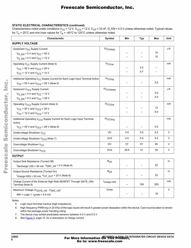
STATIC ELECTRICAL CHARACTERISTICS (continued)Characteristics noted under conditions VCC = 12 V, VCC2 = 12 V, CCP = 33 nF, G_EN = 4.5 V unless otherwise noted. Typical values for TA = 25°C and min/max values for TA = -40°C to 125°C unless otherwise noted.
Characteristic Symbol Min Typ Max Unit
SUPPLY VOLTAGE
Quiescent VCC Supply Current
VG_EN = 0 V and VCC = 55 V
VG_EN = 0 V and VCC = 12 V
IVCCsleep––
––
1010
µA
Operating VCC Supply Current (Note 5)
VCC = 55 V and VCC2 = 28 V
VCC = 12 V and VCC2 = 12 V
IVCCop––
2.20.7
––
mA
Additional Operating VCC Supply Current for Each Logic Input Terminal Active
VCC = 55 V and VCC2 = 28 V (Note 6)
IVCClog– – 5.0
mA
Quiescent VCC2 Supply Current
VG_EN = 0 V and VCC = 12 V
VG_EN = 0 V and VCC = 28 V
IVCC2sleep––
––
5.05.0
µA
Operating VCC2 Supply Current (Note 5)
VCC = 55 V and VCC2 = 28 V
VCC = 12 V and VCC2 = 12 V
IVCC2op––
––
129.0
mA
Additional Operating VCC2 Supply Current for Each Logic Input Terminal Active
VCC = 55 V and VCC2 = 28 V (Note 6)
IVCC2log
– – 5.0
mA
Undervoltage Shutdown VCC UV 4.0 5.0 5.5 V
Undervoltage Shutdown VCC2 (Note 7) UV2 4.0 5.0 5.5 V
Overvoltage Shutdown VCC OV 57 61 65 V
Overvoltage Shutdown VCC2 OV2 29.5 31 35 V
OUTPUT
Output Sink Resistance (Turned Off) Idischarge LSS = 50 mA, VSRC_HS = 0 V (Note 8)
RDS– – 22
Ω
Output Source Resistance (Turned On)Icharge HSS = 50 mA, VCP_OUT = 20 V (Note 8)
RDS– – 22
Ω
Charge Current of the External High-Side MOSFET Through GATE_HSn Terminal (Note 8)
Icharge HSS– 100 200
mA
Maximum Voltage (VGATE_HS - VSRC_HS)
INH = Logic 1, ISmax = 5.0 mA
Vmax– – 18
V
Notes5. Logic input terminal inactive (high impedance).6. High-frequency PWM-ing (» 20 kHz) of the logic inputs will result in greater power dissipation within the device. Care must be taken to remain
within the package power handling rating.7. The device may exhibit predictable behavior between 4.0 V and 5.5 V.8. See Figure 3, page 10, for a description of charge current.
Fre
esc
ale
Se
mic
on
du
cto
r, I
Freescale Semiconductor, Inc.
For More Information On This Product, Go to: www.freescale.com
nc
...
MOTOROLA ANALOG INTEGRATED CIRCUIT DEVICE DATA 338837
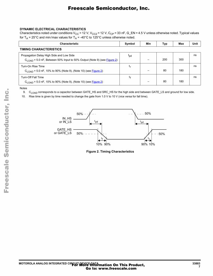
Figure 2. Timing Characteristics
DYNAMIC ELECTRICAL CHARACTERISTICSCharacteristics noted under conditions VCC = 12 V, VCC2 = 12 V, CCP = 33 nF, G_EN = 4.5 V unless otherwise noted. Typical values for TA = 25°C and min/max values for TA = -40°C to 125°C unless otherwise noted.
Characteristic Symbol Min Typ Max Unit
TIMING CHARACTERISTICS
Propagation Delay High Side and Low SideCLOAD = 5.0 nF, Between 50% Input to 50% Output (Note 9) (see Figure 2)
tpd– 200 300
ns
Turn-On Rise TimeCLOAD = 5.0 nF, 10% to 90% (Note 9), (Note 10) (see Figure 2)
tr– 80 180
ns
Turn-Off Fall TimeCLOAD = 5.0 nF, 10% to 90% (Note 9), (Note 10) (see Figure 2)
tf– 80 180
ns
Notes9. CLOAD corresponds to a capacitor between GATE_HS and SRC_HS for the high side and between GATE_LS and ground for low side.
10. Rise time is given by time needed to change the gate from 1.0 V to 10 V (vice versa for fall time).
50%50%
90%
tf
IN_HS
GATE_HS
10%
50% 50%
90% 10%
tpdtpd
tr
or IN_LS
or GATE_LS
Fre
esc
ale
Se
mic
on
du
cto
r, I
Freescale Semiconductor, Inc.
For More Information On This Product, Go to: www.freescale.com
nc
...
33883 MOTOROLA ANALOG INTEGRATED CIRCUIT DEVICE DATA8
SYSTEM/APPLICATION INFORMATION
INTRODUCTION
The 33883 is an H-bridge gate driver (or full-bridge predriver) with integrated charge pump and independent high- and low-side driver channels. It has the capability to drive large gate-
charge MOSFETs and supports high PWM frequency. In sleep mode its supply current is very low.
FUNCTIONAL TERMINAL DESCRIPTION
Supply Voltage Terminals (VCC and VCC2)
The VCC and VCC2 terminals are the power supply inputs to the device. VCC is used for the output high-side drivers and the charge pump. VCC2 is used for the linear regulation. They can be connected together or independent with different voltage values. The device can operate with VCC up to 55 V and VCC2 up to 28 V.
The VCC and VCC2 terminals have undervoltage (UV) and overvoltage (OV) shutdown. If one of the supply voltage drops below the undervoltage threshold or rises above the overvoltage threshold, the gate outputs are switched LOW in order to switch off the external MOSFETs. When the supply returns to a level that is above the UV threshold or below the OV threshold, the device resumes normal operation according to the established condition of the input terminals.
Input High- and Low-Side Terminals (IN_HSn and IN_LSn)
The IN_HSn and IN_LSn terminals are input control terminals used to control the gate outputs. These terminals are 5.0 V CMOS-compatible inputs with hysteresis. IN_HSn and IN_LSn independently control GATE_HSn and GATE_LSn, respectively.
During wake-up, the logic is supplied from the G_EN terminal. There is no internal circuit to prevent the external high-side and low-side MOSFETs from conducting at the same time.
Source Output High-Side Terminals (SRC_HSn)The SRC_HSn terminals are the sources of the external
high-side MOSFETs. The external high-side MOSFETs are controlled using the IN_HSn inputs.
Gate High- and Low-Side Terminals (GATE_HSn and GATE_LSn)
The GATE_HSn and GATE_LSn terminals are the gates of the external high- and low-side MOSFETs. The external high- and low-side MOSFETs are controlled using the IN_HSn and IN_LSn inputs.
G_EN TerminalThe G_EN terminal is used to place the device in a sleep
mode. When the G_EN terminal voltage is a logic LOW state, the device is in sleep mode. The device is enabled and fully operational when the G_EN terminal voltage is logic HIGH, typically 5.0 V.
Charge Pump Out Terminal (CP_OUT)The CP_OUT terminal is used to connect an external
reservoir capacitor for the charge pump.
Charge Pump Capacitor Terminals (C1 and C2)The C1 and C2 terminals are used to connect an external
capacitor for the charge pump.
Linear Regulator Output Terminal (LR_OUT)The LR_OUT terminal is the output of the internal regulator.
It is used to connect an external capacitor.
Ground Terminals (GNDn and GND_A)These terminals are the ground terminals of the device. They
should be connected together with a very low impedance connection.
Fre
esc
ale
Se
mic
on
du
cto
r, I
Freescale Semiconductor, Inc.
For More Information On This Product, Go to: www.freescale.com
nc
...
MOTOROLA ANALOG INTEGRATED CIRCUIT DEVICE DATA 338839
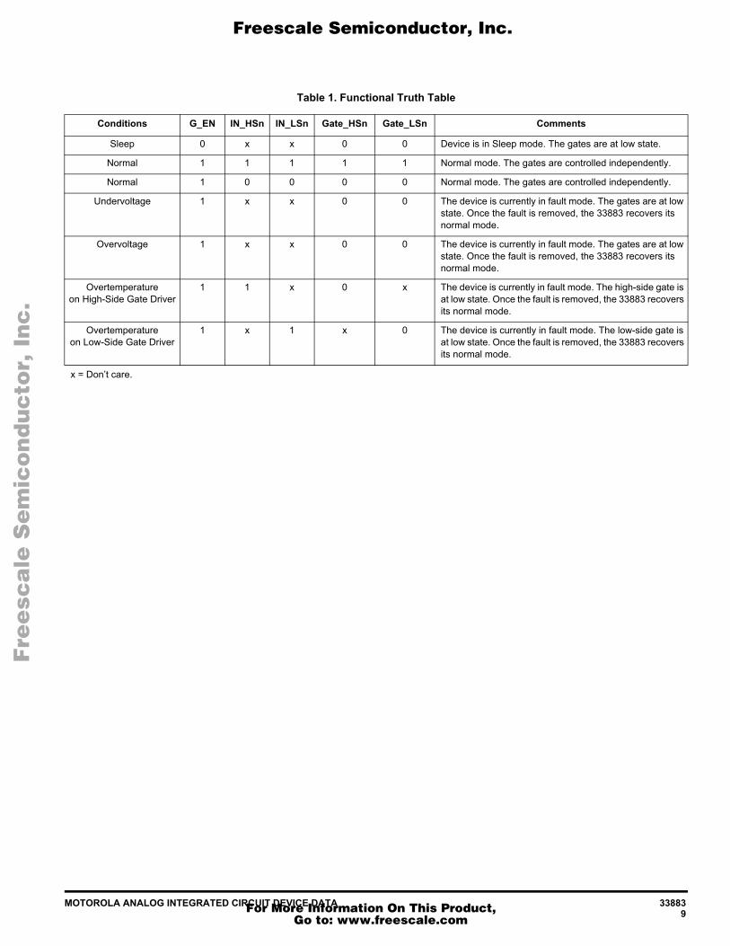
Table 1. Functional Truth Table
Conditions G_EN IN_HSn IN_LSn Gate_HSn Gate_LSn Comments
Sleep 0 x x 0 0 Device is in Sleep mode. The gates are at low state.
Normal 1 1 1 1 1 Normal mode. The gates are controlled independently.
Normal 1 0 0 0 0 Normal mode. The gates are controlled independently.
Undervoltage 1 x x 0 0 The device is currently in fault mode. The gates are at low state. Once the fault is removed, the 33883 recovers its normal mode.
Overvoltage 1 x x 0 0 The device is currently in fault mode. The gates are at low state. Once the fault is removed, the 33883 recovers its normal mode.
Overtemperatureon High-Side Gate Driver
1 1 x 0 x The device is currently in fault mode. The high-side gate is at low state. Once the fault is removed, the 33883 recovers its normal mode.
Overtemperatureon Low-Side Gate Driver
1 x 1 x 0 The device is currently in fault mode. The low-side gate is at low state. Once the fault is removed, the 33883 recovers its normal mode.
x = Don’t care.
Fre
esc
ale
Se
mic
on
du
cto
r, I
Freescale Semiconductor, Inc.
For More Information On This Product, Go to: www.freescale.com
nc
...

33883 MOTOROLA ANALOG INTEGRATED CIRCUIT DEVICE DATA10
DEVICE DESCRIPTION
Driver CharacteristicsFigure 3 represents the external circuit of the high-side gate
driver. In the schematic, HSS represents the switch that is used to charge the external high-side MOSFET through the GATE_HS terminal. LSS represents the switch that is used to discharge the external high-side MOSFET through the GATE_HS terminal. The same schematic can be applied to the external low-side MOSFET driver simply by replacing terminal CP_OUT with terminal LR_OUT, terminal GATE_HS with terminal GATE_LS, and terminal SRC_HS with GND.
Figure 3. High-Side Gate Driver Functional Schematic
The different voltages and current of the high-side gate driver are illustrated in Figure 4. The output driver sources a peak current of up to 1.0 A for 200 ns to turn on the gate. After 200 ns, 100 mA is continuously provided to maintain the gate charged. The output driver sinks a high current to turn off the gate. This current can be up to 1.0 A peak for a 100 nF load.
Note GATE_HS is loaded with a 100 nF capacitor in the chronograms. A smaller load will give lower peak and DC charge or discharge currents.
Figure 4. High-Side Gate Driver Chronograms
HSS
CP_OUT
IGATE_HSIcharge HSS
Idischarge LSS
GATE_HS1
LSS
SRC_HS1
180kΩ
18VHSSpulse_IN
LSS_IN
HSSDC_IN
IN_HS1
1.0 A Peak
1.0 A Peak100 mA Typical
0
0
0
0
0
0
1.0 A Peak100 mA Typical
-1.0 A Peak
IN_HS1
HSSpulse_IN
HSS DC_IN
LSS_IN
Idischarge LSS
IGATE_HS
Icharge HSS
Fre
esc
ale
Se
mic
on
du
cto
r, I
Freescale Semiconductor, Inc.
For More Information On This Product, Go to: www.freescale.com
nc
...
MOTOROLA ANALOG INTEGRATED CIRCUIT DEVICE DATA 3388311
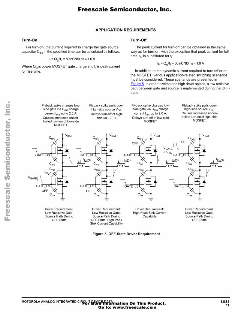
APPLICATION REQUIREMENTS
Turn-OnFor turn-on, the current required to charge the gate source
capacitor Ciss in the specified time can be calculated as follows:
IP = Qg/tr = 80 nC/80 ns ≈ 1.0 A
Where Qg is power MOSFET gate charge and tr is peak current for rise time.
Turn-OffThe peak current for turn-off can be obtained in the same
way as for turn-on, with the exception that peak current for fall time, tf, is substituted for tr:
IP = Qg/tf = 80 nC/80 ns ≈ 1.0 A
In addition to the dynamic current required to turn off or on the MOSFET, various application-related switching scenarios must be considered. These scenarios are presented in Figure 5. In order to withstand high dV/dt spikes, a low resistive path between gate and source is implemented during the OFF-state.
Figure 5. OFF-State Driver Requirement
Driver Requirement: Low Resistive Gate-Source Path During
OFF-State
Flyback spike charges low-side gate via Crss charge current Irss up to 2.0 A.
Causes increased uncon-trolled turn-on of low-side
MOSFET.
Ciss
Ciss
Crss
Crss
VBAT
Driver Requirement: Low Resistive Gate-Source Path During
OFF-State. High Peak Sink Current Capability
Flyback spike pulls down high-side source VGS.Delays turn-off of high-
side MOSFET.
Ciss
Ciss
Crss
Crss
VBAT
Driver Requirement:High Peak Sink Current
Capability
Flyback spike charges low-side gate via Crss charge current Irss up to 2.0 A.
Delays turn-off of low-side MOSFET.
Ciss
Ciss
Crss
Crss
VBAT
Driver Requirement:Low Resistive Gate-Source Path During
OFF-State
Ciss
Ciss
Crss
Crss
VBAT
Flyback spike pulls down high-side source VGS.
Causes increased uncon-trolled turn-on of high-side
MOSFET.
OFF OFF
OFF OFF
GATE_LS
ILOADL1ILOADL1
ILOADL1ILOADL1
Irss
VGATE
VGATE-VDRN
GATE_HS
GATE_LS
GATE_HS GATE_HS
GATE_LS
GATE_HS
GATE_LS
Fre
esc
ale
Se
mic
on
du
cto
r, I
Freescale Semiconductor, Inc.
For More Information On This Product, Go to: www.freescale.com
nc
...
33883 MOTOROLA ANALOG INTEGRATED CIRCUIT DEVICE DATA12
Low-Drop Linear RegulatorThe low-drop linear regulator is supplied by VCC2. If VCC2
exceeds 15.0 V, the output is limited to 14.5 V (typical).
The low-drop linear regulator provides the 5.0 V for the logic section of the driver, the Vgs_ls buffered at LR_OUT, and the +14.5 V for the charge pump, which generates the CP_OUT The low-drop linear regulator provides 4.0 mA average current per driver stage.
In case of the full bridge, that means approximately 16 mA —8.0 mA for the high side and 8.0 mA for the low side.
Note: The average current required to switch a gate with a frequency of 100 kHz is:
ICP = Qg * fPWM = 80 nC * 100 kHz = 8.0 mA
In a full-bridge application only one high side and one low side switches on or off at the same time.
Charge PumpThe charge pump generates the high-side driver supply
voltage (CP_OUT), buffered at CCP_OUT. Figure 6 shows the charge pump basic circuit without load.
Figure 6. Charge Pump Basic Circuit
When the oscillator is in low state [(1) in Figure 6], CCP is charged through D2 until its voltage reaches VCC - VD2. When the oscillator is in high state (2), CCP is discharged though D1 in CCP_OUT, and final voltage of the charge pump, VCP_OUT, is Vcc + VLR_OUT - 2VD. The frequency of the 33883 oscillator is about 330 kHz.
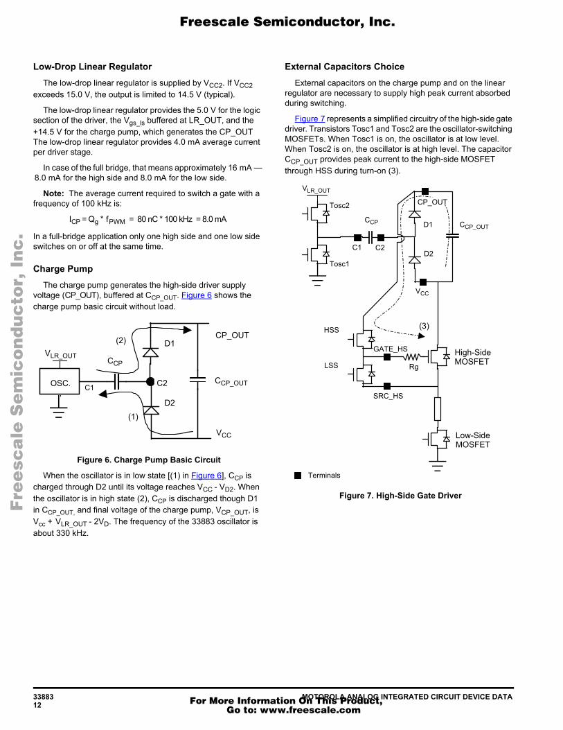
External Capacitors ChoiceExternal capacitors on the charge pump and on the linear
regulator are necessary to supply high peak current absorbed during switching.
Figure 7 represents a simplified circuitry of the high-side gate driver. Transistors Tosc1 and Tosc2 are the oscillator-switching MOSFETs. When Tosc1 is on, the oscillator is at low level. When Tosc2 is on, the oscillator is at high level. The capacitor CCP_OUT provides peak current to the high-side MOSFET through HSS during turn-on (3).
Figure 7. High-Side Gate Driver
Osc.
Vbat
VCP_OUT
Ccp_out
VLR_OUT Ccp
D1
D2
A
(1)
(2)VLR_OUT
OSC.
CCP
VCC
CP_OUT
CCP_OUTC2
D2
D1
C1
Ccp_out
VLR-OUT
Ccp D1
D2 C1
Vcc
C2
CP_out
SRC_HS
HS MOSFET
LS MOSFET
T1
T2 Rg
Tosc1
Tosc2
GATE_HS
pins
(3)
High-SideMOSFET
Low-SideMOSFET
SRC_HS
GATE_HS
VCC
C1 C2
CCP
D2
D1
CP_OUT
VLR_OUT
Tosc2
Tosc1
HSS
LSS
Terminals
CCP_OUT
Rg
Fre
esc
ale
Se
mic
on
du
cto
r, I
Freescale Semiconductor, Inc.
For More Information On This Product, Go to: www.freescale.com
nc
...

MOTOROLA ANALOG INTEGRATED CIRCUIT DEVICE DATA 3388313
CCP
CCP choice depends on power MOSFET characteristics and the working switching frequency. Figure 8 contains two diagrams that depict the influence of CCP value on VCP_OUT average voltage level. The diagrams represent two different frequencies for two power MOSFETs, MTP60N06HD and MPT36N06V.
Figure 8. VCP_OUT Versus CCP
The smaller the CCP value is, the smaller the VCP_OUT value is. Moreover, for the same CCP value, when the switching frequency increases, the average VCP_OUT level decreases. For most of the applications, a typical value of 33 nF is recommended.
CCP_OUT
Figure 9 depicts the simplified CCP_OUT current and voltage waveforms. fPWM is the working switching frequency.
Figure 9. Simplified CCP_OUT Current and Voltage Waveforms
As shown above, at high-side MOSFET turn-on VCP_OUT voltage decreases. This decrease can be calculated according to the CCP_OUT value as follows:
Where Qg is power MOSFET gate charge.
CLR_OUT
CLR_OUT provides peak current needed by the low-side MOSFET turn-on. VLR_OUT decrease is as follows:
Typical Values of CapacitorsIn most working cases the following typical values are
recommended for a well-performing charge pump:
CCP = 33 nF, CCP_OUT = 470 nF, and CLR_OUT = 470 nF
These values give a typical 100 mV voltage ripple on VCP_OUT and VLR_OUT with Qg = 50 nC.
MTP60N06HD (Qg=50nC)
18.5
19
19.5
20
20.5
21
21.5
5 25 45 65 85
Ccp (nF)
Vcp_
out (
V)
20 kHz 100 kHz
18
18.5
19
19.5
20
20.5
21
5 25 45 65 85
Ccp (nF)
Vcp_
out (
v)
20KhZ100 KhZ
MTP60N06HD (Qg = 50 nC)
MTP36N06V (Qg = 40 nC)
MTP60N06HD (Qg = 50 nC)
CCP (nF)
V CP_
OU
T (V
)
CCP (nF)
V CP_
OU
T (V
)
20 kHz100 kHz
VCp_out
Oscillatorin highstate Oscillator
in lowstate
ICp_out
PeakCurrent
f=330kHz fPWM
outCcpV _∆
High Sideturn on
rage VCp_out
Oscillatorin HighState Oscillator
in LowState
f = 330 kHz fPWM
∆VCP_OUT
High Side Turn OnVCP_OUT
VCP_OUTAverage
ICP_OUT
Peak Current
∆VCP_OUT = CCP_OUT
Qg
∆VLR_OUT = CLR_OUT
Qg
Fre
esc
ale
Se
mic
on
du
cto
r, I
Freescale Semiconductor, Inc.
For More Information On This Product, Go to: www.freescale.com
nc
...

33883 MOTOROLA ANALOG INTEGRATED CIRCUIT DEVICE DATA14
Protection
Gate Protection
The low-side driver is supplied from the built-in low-drop regulator. The high-side driver is supplied from the internal charge pump buffered at CP_OUT.
The low-side gate is protected by the internal linear regulator, which ensures that VGATE_LS does not exceed the maximum VGS. Especially when working with the charge pump, the voltage at CP_OUT can be up to 65 V. The high-side gate is clamped internally in order to avoid a VGS exceeding 18 V.
Gate protection does not include a flyback voltage clamp that protects the driver and the external MOSFET from a flyback voltage that can occur when driving inductive load. This flyback voltage can reach high negative voltage values and needs to be clamped externally, as shown in Figure 10.
Figure 10. Gate Protection and Flyback Voltage Clamp
Load Dump and Reverse Battery
VCC and VCC2 can sustain load a dump pulse of 40 V and double battery of 24 V. Protection against reverse polarity is ensured by the external power MOSFET with the free-wheeling diodes forming a conducting pass from ground to VCC. Additional protection is not provided within the circuit. To protect the circuit an external diode can be put on the battery line. It is not recommended putting the diode on the ground line.
Temperature Protection
There is temperature shutdown protection per each half-bridge. Temperature shutdown protects the circuitry against temperature damage by switching off the output drivers. Its typical value is 175°C with an hysteresis of 15°C.
dV/dt at VCC
VCC voltage must be higher than (SRC_HS voltage minus a diode drop voltage) to avoid perturbation of the high-side driver.
In some applications a large dV/dt at terminal C2 owing to sudden changes at VCC can cause large peak currents flowing through terminal C1, as shown in Figure 11.
For positive transitions at terminal C2, the absolute value of the minimum peak current, IC1min, is specified at 2.0 A for a tC1min duration of 600 ns.
For negative transitions at terminal C2, the maximum peak current, IC1max, is specified at 2.0 A for a tC1max duration of 600 ns. Current sourced by terminal C1 during a large dV/dt will result in a negative voltage at terminal C1 (Figure 11). The minimum peak voltage VC1min is specified at -1.5 V for a duration of tC1max = 600 ns. A series resistor with the charge pump capacitor (Ccp) capacitor can be added in order to limit the surge current.
Figure 11. Limits of C1 Current and Voltage with Large Values of dV/dt
OutputDriver
OUT
OutputDriver
OUTIN
L1
M2
GATE_LS
SRC_HS
GATE_HS
InductiveFlyback Voltage
Clamp
IN
Dcl
M1 VCC
CP_OUTLR_OUT
VGS < 14 VUnder All
Conditions
tC1max
tC1min
VCC
I(C1+C2)
IC1max
IC1min
V(LR_OUT)
0 VV(C1)
0 A
VC1min
Fre
esc
ale
Se
mic
on
du
cto
r, I
Freescale Semiconductor, Inc.
For More Information On This Product, Go to: www.freescale.com
nc
...

MOTOROLA ANALOG INTEGRATED CIRCUIT DEVICE DATA 3388315
In the case of rapidly changing VCC voltages, the large dV/dt may result in perturbations of the high-side driver, thereby forcing the driver into an OFF state. The addition of capacitors C3 and C4, as shown in Figure 12, reduces the dV/dt of the source line, consequently reducing driver perturbation. Typical values for R3/R4 and C3/C4 are 10 Ω and 10 nF, respectively.
dV/dt at VCC2
When the external high-side MOSFET is on, in case of rapid negative change of VCC2 the voltage (VGATE_HS - VSRC_HS) can be higher than the specified 18 V. In this case a resistance in the SRC line is necessary to limit the current to 5.0 mA max. It will protect the internal zener placed between GATE_HS and SRC terminals.
Figure 12. Application Schematic with External Protection Circuit
IN_LS2
IN_HS2
IN_LS1
IN_HS1
VBAT
G_EN
C1C2
CCP
CLR_OUT
CCP_OUT
MCU
VCC2
VCC
VBOOST
33883
M1
M2
M3
M4
R1 R2470 nF
470 nF 50 Ω
50 Ω
50 Ω
50 Ω
33 nF
DC
Motor
R3
10 Ω10 nFC3
10 nFC4 10 Ω
R4
IN_LS2
IN_HS2
IN_LS1
IN_HS1
G_ENC1
C2
VCC2
VCC
GND
GATE_LS2
SRC_HS2GATE_HS2GATE_LS1
SRC_HS1
GATE_HS1
LR_OUTCP_OUT
Fre
esc
ale
Se
mic
on
du
cto
r, I
Freescale Semiconductor, Inc.
For More Information On This Product, Go to: www.freescale.com
nc
...

33883 MOTOROLA ANALOG INTEGRATED CIRCUIT DEVICE DATA16
PACKAGE DIMENSIONS
DIMENSIONS ARE IN MILLIMETERS.DIMENSIONING AND TOLERANCING PER ASME Y14.5M, 1994.DATUMS A AND B TO BE DETERMINED AT THE PLANE WHERE THE BOTTOM OF THE LEADS EXIT THE PLASTIC BODY.THIS DIMENSION DOES NOT INCLUDE MOLD FLASH, PROTRUSION OR GATE BURRS. MOLD FLASH, PROTRUSION OR GATE BURRS SHALL NOT EXCEED 0.15mm PER SIDE. THIS DIMENSION IS DETERMINED AT THE PLANE WHERE THE BOTTOM OF THE LEADS EXIT THE PLASTIC BODY.THIS DIMENSION DOES NOT INCLUDE INTER-LEAD FLASH OR PROTRUSIONS. INTER-LEAD FLASH AND PROTRUSIONS SHALL NOT EXCEED 0.25mm PER SIDE. THIS DIMENSION IS DETERMINED AT THE PLANE WHERE THE BOTTOM OF THE LEADS EXIT THE PLASTIC BODY.THIS DIMENSION DOES NOT INCLUDE DAMBAR PROTRUSION. ALLOWABLE DAMBAR PROTRUSION SHALL NOT CAUSE THE LEAD WIDTH TO EXCEED 0.62mm.
10 11
1 20
SEATINGPLANE
7
0.75 X45
10X
M0.25 B
0.4920X
BM0.25 AT
4
10.5510.05
12.9512.65
A
7.67.4 B
PIN 1 INDEX
PIN'SNUMBER
5
AA
0.25
1.00.4
0
0.320.23
SECTION A-A
0.35
2.652.35 0.25
0.106
T20X
0.1 T
1.2718X
1. 2. 3. 4. 5. 6.
NOTES:
DW SUFFIX20-TERMINAL SOICWPLASTIC PACKAGE
CASE 751D-06ISSUE H
Fre
esc
ale
Se
mic
on
du
cto
r, I
Freescale Semiconductor, Inc.
For More Information On This Product, Go to: www.freescale.com
nc
...
MOTOROLA ANALOG INTEGRATED CIRCUIT DEVICE DATA 3388317
NOTES
Fre
esc
ale
Se
mic
on
du
cto
r, I
Freescale Semiconductor, Inc.
For More Information On This Product, Go to: www.freescale.com
nc
...

33883 MOTOROLA ANALOG INTEGRATED CIRCUIT DEVICE DATA18
NOTES
Fre
esc
ale
Se
mic
on
du
cto
r, I
Freescale Semiconductor, Inc.
For More Information On This Product, Go to: www.freescale.com
nc
...

MOTOROLA ANALOG INTEGRATED CIRCUIT DEVICE DATA 3388319
NOTES
Fre
esc
ale
Se
mic
on
du
cto
r, I
Freescale Semiconductor, Inc.
For More Information On This Product, Go to: www.freescale.com
nc
...

Information in this document is provided solely to enable system and software implementers to use Motorola products. There are no express or impliedcopyright licenses granted hereunder to design or fabricate any integrated circuits or integrated circuits based on the information in this document.
Motorola reserves the right to make changes without further notice to any products herein. Motorola makes no warranty, representation or guaranteeregarding the suitability of its products for any particular purpose, nor does Motorola assume any liability arising out of the application or use of any productor circuit, and specifically disclaims any and all liability, including without limitation consequential or incidental damages. “Typical” parameters which may beprovided in Motorola data sheets and/or specifications can and do vary in different applications and actual performance may vary over time. All operatingparameters, including “Typicals” must be validated for each customer application by customer’s technical experts. Motorola does not convey any licenseunder its patent rights nor the rights of others. Motorola products are not designed, intended, or authorized for use as components in systems intended forsurgical implant into the body, or other applications intended to support or sustain life, or for any other application in which the failure of the Motorola productcould create a situation where personal injury or death may occur. Should Buyer purchase or use Motorola products for any such unintended orunauthorized application, Buyer shall indemnify and hold Motorola and its officers, employees, subsidiaries, affiliates, and distributors harmless against allclaims, costs, damages, and expenses, and reasonable attorney fees arising out of, directly or indirectly, any claim of personal injury or death associatedwith such unintended or unauthorized use, even if such claim alleges that Motorola was negligent regarding the design or manufacture of the part.
MOTOROLA and the Stylized M Logo are registered in the US Patent and Trademark Office. All other product or service names are the property of theirrespective owners.
© Motorola, Inc. 2004
HOW TO REACH US:
USA/EUROPE/LOCATIONS NOT LISTED: JAPAN: Motorola Japan Ltd.; SPS, Technical Information CenterMotorola Literature Distribution 3-20-1 Minami-Azabu. Minato-ku, Tokyo 106-8573, JapanP.O. Box 5405, Denver, Colorado 80217 81-3-3440-35691-800-521-6274 or 480-768-2130
ASIA/PACIFIC: Motorola Semiconductors H.K. Ltd.; Silicon Harbour Centre2 Dai King Street, Tai Po Industrial Estate, Tai Po, N.T., Hong Kong852-26668334
HOME PAGE: http://motorola.com/semiconductors
MC33883/D
Fre
esc
ale
Se
mic
on
du
cto
r, I
Freescale Semiconductor, Inc.
For More Information On This Product, Go to: www.freescale.com
nc
...