30
13
IEEE TRANSACTIONS ON INDUSTRIAL ELECTRONICS, VOL. 59, NO. 2, FEBRUARY 2012 655 A New Multilevel Converter Topology With Reduced Number of Power Electronic Components Javad Ebrahimi, Student Member, IEEE, Ebrahim Babaei, Member, IEEE, and Gevorg B. Gharehpetian, Senior Member, IEEE Abstract—In this paper, a new topology for cascaded multilevel converter based on submultilevel converter units and full-bridge converters is proposed. The proposed topology significantly re- duces the number of dc voltage sources, switches, IGBTs, and power diodes as the number of output voltage levels increases. Also, an algorithm to determine dc voltage sources magnitudes is proposed. To synthesize maximum levels at the output voltage, the proposed topology is optimized for various objectives, such as the minimization of the number of switches, gate driver circuits and capacitors, and blocking voltage on switches. The analytical analyses of the power losses of the proposed converter are also pre- sented. The operation and performance of the proposed multilevel converter have been evaluated with the experimental results of a single-phase 125-level prototype converter. Index Terms—Bidirectional switch, cascaded multilevel con- verter, full-bridge converter, multilevel converter, submultilevel converter. I. I NTRODUCTION T HE basic concept of a multilevel converter is to use a series of power semiconductor switches that properly connected to several lower dc voltage sources to synthesize a near sinusoidal staircase voltage waveform. The small output voltage step results in high quality output voltage, reduction of voltage stresses on power switching devices, lower switching losses and higher efficiency. Numerous multilevel converter topologies and wide variety of control methods have been developed in the recent literature [1]–[4]. Three different basic multilevel converter topologies are the neutral point clamped (NPC) or diode clamped [5], the flying capacitor (FC) or capacitor clamped [6] and the cascaded H-bridge (CHB) [7]. The main drawbacks of NPC topology are their unequal voltage sharing among series connected capaci- tors that result in dc-link capacitor unbalancing and requiring a great number of clamping diodes for higher level. The FC multilevel converter uses flying capacitor as clamping devices. These topologies have several attractive properties in compar- ison with the NPC converter, including the advantage of the transformerless operation and redundant phase leg states that Manuscript received May 27, 2010; revised September 22, 2010, January 2, 2011, and March 18, 2011; accepted March 28, 2011. Date of publication May 5, 2011; date of current version October 18, 2011. This work was supported by the Iran Renewable Energy Organization (SUNA), Tehran, Iran. J. Ebrahimi and G. B. Gharehpetian are with the Electrical Engineering Department, Amirkabir University of Technology, Tehran 15914, Iran (e-mail: [email protected]; [email protected]). E. Babaei (corresponding author) is with the Faculty of Electrical and Com- puter Engineering, University of Tabriz, Tabriz 51664, Iran (e-mail: e-babaei@ tabrizu.ac.ir). Digital Object Identifier 10.1109/TIE.2011.2151813 allow the switching stresses to be equally distributed between semiconductor switches [8], [9]. But, these converters require an excessive number of storage capacitors for higher voltage steps. The CHB topologies are proper option for high level applications from point of view of modularity and simplicity of control. But, in this topology, a large number of isolated dc voltage sources are required to supply each conversion cell. It increases the converter cost and complexity. In multilevel converter, the power quality is improved as the number of levels increases at the output voltage. However, it causes to the increasing number of switching devices and other components, and increases the cost and control complexity and tends to reduce the overall reliability and efficiency of the converter. It is noticeable that multilevel converters can sustain the operation in case of internal fault [10]. In the case of internal fault of one cell of FC converter, the maximum output voltage remains constant, but the number of levels decreases. On the other hand, when an internal fault is detected in the CHB converter, and the faulty cell is identified, it can be easily isolated through an external switch and replaced by a new operative cell [11]. Asymmetric and/or hybrid multilevel converters have been presented in [12], [13]. In the asymmetric topologies, the values of dc voltage sources magnitudes are unequal or changed dynamically [14]. These converters reduce the size and cost of the converter and improve the reliability since fewer semi- conductors and capacitors are employed [15]. The hybrid multilevel converters are composed of different multilevel topologies with unequal values of dc voltage sources and dif- ferent modulation techniques and/or semiconductor technolo- gies [12]. With appropriate selection of switching devices, the converter cost is significantly reduced. But, the application of different multilevel topologies result in loss of modularity and produces problems with switching frequency and restrictions on the modulation and control method [16]. The researchers are strived in [17] and [18] to introduce a new topology for multilevel converters with a reduced number of components compared to conventional multilevel converters. This topology is composed of modular submultilevel converters that makes it easily extensible to higher number of output voltage levels without undue increase in the power circuit complexity and reduces controller design cost. By the presented algorithm in [17] and [18], it is not possible to create all levels (odd and even) at the output voltage, and it reduces the flexibility of the converter. Also, to create the output voltage with a constant number of levels, the converter needs many large numbers of bidirectional switches. To overcome these 0278-0046/$26.00 © 2011 IEEE
-
Upload
vinay-kumar -
Category
Documents
-
view
12 -
download
7
Transcript of 30

IEEE TRANSACTIONS ON INDUSTRIAL ELECTRONICS, VOL. 59, NO. 2, FEBRUARY 2012 655
A New Multilevel Converter Topology With ReducedNumber of Power Electronic Components
Javad Ebrahimi, Student Member, IEEE, Ebrahim Babaei, Member, IEEE, andGevorg B. Gharehpetian, Senior Member, IEEE
Abstract—In this paper, a new topology for cascaded multilevelconverter based on submultilevel converter units and full-bridgeconverters is proposed. The proposed topology significantly re-duces the number of dc voltage sources, switches, IGBTs, andpower diodes as the number of output voltage levels increases.Also, an algorithm to determine dc voltage sources magnitudesis proposed. To synthesize maximum levels at the output voltage,the proposed topology is optimized for various objectives, such asthe minimization of the number of switches, gate driver circuitsand capacitors, and blocking voltage on switches. The analyticalanalyses of the power losses of the proposed converter are also pre-sented. The operation and performance of the proposed multilevelconverter have been evaluated with the experimental results of asingle-phase 125-level prototype converter.
Index Terms—Bidirectional switch, cascaded multilevel con-verter, full-bridge converter, multilevel converter, submultilevelconverter.
I. INTRODUCTION
THE basic concept of a multilevel converter is to usea series of power semiconductor switches that properly
connected to several lower dc voltage sources to synthesize anear sinusoidal staircase voltage waveform. The small outputvoltage step results in high quality output voltage, reduction ofvoltage stresses on power switching devices, lower switchinglosses and higher efficiency.
Numerous multilevel converter topologies and wide varietyof control methods have been developed in the recent literature[1]–[4]. Three different basic multilevel converter topologiesare the neutral point clamped (NPC) or diode clamped [5], theflying capacitor (FC) or capacitor clamped [6] and the cascadedH-bridge (CHB) [7]. The main drawbacks of NPC topology aretheir unequal voltage sharing among series connected capaci-tors that result in dc-link capacitor unbalancing and requiringa great number of clamping diodes for higher level. The FCmultilevel converter uses flying capacitor as clamping devices.These topologies have several attractive properties in compar-ison with the NPC converter, including the advantage of thetransformerless operation and redundant phase leg states that
Manuscript received May 27, 2010; revised September 22, 2010, January 2,2011, and March 18, 2011; accepted March 28, 2011. Date of publicationMay 5, 2011; date of current version October 18, 2011. This work wassupported by the Iran Renewable Energy Organization (SUNA), Tehran, Iran.
J. Ebrahimi and G. B. Gharehpetian are with the Electrical EngineeringDepartment, Amirkabir University of Technology, Tehran 15914, Iran (e-mail:[email protected]; [email protected]).
E. Babaei (corresponding author) is with the Faculty of Electrical and Com-puter Engineering, University of Tabriz, Tabriz 51664, Iran (e-mail: [email protected]).
Digital Object Identifier 10.1109/TIE.2011.2151813
allow the switching stresses to be equally distributed betweensemiconductor switches [8], [9]. But, these converters requirean excessive number of storage capacitors for higher voltagesteps. The CHB topologies are proper option for high levelapplications from point of view of modularity and simplicityof control. But, in this topology, a large number of isolated dcvoltage sources are required to supply each conversion cell. Itincreases the converter cost and complexity.
In multilevel converter, the power quality is improved as thenumber of levels increases at the output voltage. However, itcauses to the increasing number of switching devices and othercomponents, and increases the cost and control complexityand tends to reduce the overall reliability and efficiency ofthe converter. It is noticeable that multilevel converters cansustain the operation in case of internal fault [10]. In the case ofinternal fault of one cell of FC converter, the maximum outputvoltage remains constant, but the number of levels decreases.On the other hand, when an internal fault is detected in theCHB converter, and the faulty cell is identified, it can be easilyisolated through an external switch and replaced by a newoperative cell [11].
Asymmetric and/or hybrid multilevel converters have beenpresented in [12], [13]. In the asymmetric topologies, the valuesof dc voltage sources magnitudes are unequal or changeddynamically [14]. These converters reduce the size and costof the converter and improve the reliability since fewer semi-conductors and capacitors are employed [15]. The hybridmultilevel converters are composed of different multileveltopologies with unequal values of dc voltage sources and dif-ferent modulation techniques and/or semiconductor technolo-gies [12]. With appropriate selection of switching devices, theconverter cost is significantly reduced. But, the application ofdifferent multilevel topologies result in loss of modularity andproduces problems with switching frequency and restrictionson the modulation and control method [16].
The researchers are strived in [17] and [18] to introduce anew topology for multilevel converters with a reduced numberof components compared to conventional multilevel converters.This topology is composed of modular submultilevel convertersthat makes it easily extensible to higher number of outputvoltage levels without undue increase in the power circuitcomplexity and reduces controller design cost. By the presentedalgorithm in [17] and [18], it is not possible to create alllevels (odd and even) at the output voltage, and it reduces theflexibility of the converter. Also, to create the output voltagewith a constant number of levels, the converter needs manylarge numbers of bidirectional switches. To overcome these
0278-0046/$26.00 © 2011 IEEE

656 IEEE TRANSACTIONS ON INDUSTRIAL ELECTRONICS, VOL. 59, NO. 2, FEBRUARY 2012
Fig. 1. (a) Basic unit [19] and (b) multilevel converter presented in [19].
disadvantages, [19] has presented a new topology, which hasdecreased the number of bidirectional switches and dc voltagesource compared to [17] and [18] and with the ability ofthe production of all levels at the output voltage. The maindrawback of this topology is the utilization of unidirectionalswitches that operate in the high output voltage.
The structures, based on similar concepts, have been pre-sented in [20]. In these topologies, the dc source is formed byconnecting a number of half-bridge cells, diode-clamped phaseleg or capacitor-clamped phase leg. Also, in [21], the topologyhas been obtained from the mixture of the FC and CHB inverter.These structures provide a high number of output levels usinglow number of components. But, the main drawback of thesetopologies is the utilization a full-bridge converter, which op-erates in the high output voltage. Also, these designs are notflexible.
This paper proposes a new modular and simple topology forcascaded multilevel converter that produces a high number oflevels with the application of a low number of power electroniccomponents. Then, a procedure for calculating the values ofrequired dc voltage sources is also proposed. In addition, thestructure of the proposed topology is optimized for variousaims. Finally, a design example of the proposed multilevelconverter is included.
II. MULTILEVEL CONVERTER WITH
REDUCED NUMBER OF SWITCHES
The basic unit of the submultilevel converter, presented in[19], is illustrated in Fig. 1(a). It consists of several capacitors(with dc voltages) and bidirectional switches. If n capacitorsare used, n + 1 different values can be obtained for vo, byn + 1 bidirectional switches. The output voltage of this sub-multilevel converter has zero or positive values. The presentedunit requires bidirectional switches with the capability of block-ing voltage and conducting current in both directions. Sev-eral arrangements can be used to create bidirectional switchesconsidering of insulated gate bipolar transistors (IGBTs) anddiodes. The proper configuration of bidirectional switches isarranged by a common emitter connection of two IGBTs, which
each one of IGBTs has an antiparallel diode. Because theemitters of two IGBTs are common, the base voltage of eachIGBT can be measured versus its common emitter. Therefore,a bidirectional switch requires a gate driver circuit in thisconfiguration. This configuration of bidirectional switch is usedin this paper, to make it comparable with one presented in [19].
The cascaded connection of these submultilevel convertersincrease the possible value of vo, effectively. But, it can onlygenerate the positive output voltages. To generate both positiveand negative voltages, a full-bridge converter is connected tothe output terminal of the cascaded connection of submultilevelconverters. But, the unidirectional switches in the full-bridgeconverter and some bidirectional switches, such as S1, mustoperate at the high output voltage and need higher voltageblocking. As a result, the cost and losses will be increased andits industrial applications will be limited. Fig. 1(b) shows ksubmultilevel converters in series, where the structure of thefirst till kth submultilevel converters has n1, n2, . . . , nk bidi-rectional switches, respectively. In this case, only one switchof each submultilevel converter turns on in different operationmodes of the converter. The number of output voltage levels(Nlevel) and IGBTs (NIGBT ) are given by the followingequations, respectively:
Nlevel =2
(k∏
i=1
ni
)−1=2(n1×n2×. . . × nk)−1 (1)
NIGBT =2
(k∑
i=1
ni
)+4=2(n1+n2+. . .+nk)+4. (2)
The maximum value of the output voltage (Vomax) can beobtained, as follows:
Vomax =k∑
i=1
(ni − 1)Vi. (3)
III. PROPOSED TOPOLOGY
Fig. 2(a) shows the proposed topology for a submultilevelconverter, hereafter called multilevel module (MLM), whichis used for the implementation of the proposed multilevelconverter topology. It consists of n dc voltage sources and nbidirectional switches. A MLM produces a staircase voltagewaveform with positive polarity. It is connected to a single-phase full-bridge converter, which particularly alternates theinput voltage polarity and provides positive or negative stair-case waveform at the output. The full-bridge converter hasfour unidirectional switches, which consists of an IGBT andan antiparallel fast recovery diode. The typical output wave-forms of v′
o and vo are shown in Fig. 2(b). It is noticeablethat only one switch turns on in different operation modesof the MLM and also, both switches T1 and T4 (or T2 andT3) cannot be simultaneously turned on (expect state 1 inTable I) because of a short circuit occurrence across dc voltagesources and then the voltage vo would be produced. Table Isummarizes the values of the output voltage of a MLM and cor-responding full-bridge converter for different state of switchesS1, S2, . . . , Sn, T1, . . . , T4. State conditions 1 and 0 means that

EBRAHIMI et al.: MULTILEVEL CONVERTER TOPOLOGY WITH REDUCED POWER ELECTRONIC COMPONENTS 657
Fig. 2. (a) Proposed submultilevel topology and (b) typical output waveformof vo.
TABLE IVALUES OF vo FOR DIFFERENT STATES OF SWITCHES IN
SUBMULTILEVEL CONVERTER
the switch is on and off, respectively. For simplicity, the on-state voltage drops of switches have been neglected. As it canbe seen, 2n + 1 different values can be obtained for vo.
The proposed multilevel converter topology, which is basedon the combination of MLMs and full-bridges converters, isshown in Fig. 3. The structure of the first till kth MLM hasn1, n2, . . . , nk bidirectional switches, respectively. Each MLMcan generate a stepped voltage waveform with positive polar-ity. The full-bridge converters provide positive and negativestepped voltage waveforms in their output.
The different output voltage levels can be determined by thecombination of switching states of MLMs. It is obvious thatonly one switch of each MLM turns on in different operationmodes of the converter without considering the zero voltagestate of MLMs. If the proper values for dc voltage sourcesare selected, then, the output voltage of the converter will beobtained between −∑k
i=1
∑ni
j=1 Vij and +∑k
i=1
∑ni
j=1 Vij .Table II shows the output voltage of the proposed topologyfor different switching states. It is noticeable that there are two
Fig. 3. Proposed multilevel converter topology.
TABLE IIVALUES OF vo FOR DIFFERENT STATES OF
SWITCHES IN PROPOSED TOPOLOGY
switching states for producing the zero voltage level and in theTable II, only one of them is presented.
It should be noted that the capacitors can be replaced withthe dc voltage sources in the proposed topology. Although thistopology requires multiple dc voltage sources, but they may beavailable in some systems through renewable energy sources,such as photovoltaic panels or fuel cells, or with energy storagedevices, such as capacitors or batteries. When ac voltage isalready available, then, multiple dc sources can be generatedusing isolated transformers and rectifiers, too [19].
If the voltage sources are changed during the converteroperation, the voltage balancing should be done. For example,the output voltages of fuel cells are variable. Therefore, ifthey are used at dc-link, the quality of output voltage of theconverter will be reduced. The hardware proposed method to

658 IEEE TRANSACTIONS ON INDUSTRIAL ELECTRONICS, VOL. 59, NO. 2, FEBRUARY 2012
Fig. 4. DC-link voltage balancing.
dc-link balancing is shown in Fig. 4. The capacitor voltages arecontrolled with the DC/DC converters.
If the dc voltage sources are considered to be equal in MLMs,the structure of the proposed topology will be symmetrical. Inthe asymmetrical structure of the proposed topology, similarto the asymmetrical cascaded multilevel converter, there is onlyone switching state for each output voltage level (except thezero level) to produce unequal values for vo. In this paper, toreduce the number of components, the asymmetrical structurehas been studied. It is noticeable that the asymmetrical structurehas circulating energy problems. Therefore, if diode-basedrectifiers are used for dc voltage sources, their dc-link voltagescan increase their values dangerously [12].
Considering the first dc voltage source (V11) as the basevalue of the per-unit system, i.e.,
Vbase = V11 = Vdc (4)
then, the normalized values of the dc voltage sources forproducing all levels (odd and even) in the output must be chosenusing the following algorithm.
For module 1
V11 = Vdc (5)
V1i = V11 = Vdc, i = 2, . . . , n1. (6)
For module 2
V21 = V11 + 2n1∑i=1
V1i = (2n1 + 1)Vdc (7)
V2i = V21 = (2n1 + 1)Vdc, i = 2, . . . , n2. (8)
For module 3
V31 =V11 + 2n1∑i=1
V1i + 2n2∑i=1
V2i
= (2n1 + 1)(2n2 + 1)Vdc (9)
V3i =V31 = (2n1 + 1)(2n2 + 1)Vdc, i = 2, . . . , n3. (10)
In general, for the mth module
Vm1 = V11 + 2m−1∑i=1
ni∑j=1
Vij =m−1∏i=1
(2ni + 1)Vdc (11)
Vmi = Vm1 =m−1∏i=1
(2ni + 1)Vdc, i = 2, . . . , nm. (12)
By using the proposed algorithm, the maximum value of theoutput voltage (Vomax) is obtained, as follows:
Vomax =k∑
i=1
ni∑j=1
Vij =k∑
i=1
(ni × Vi1). (13)
The number of output voltage levels can be determined bythe following equation:
Nlevel =k∏
i=1
(2ni + 1)
= (2n1 + 1) × (2n2 + 1) × . . . × (2nk + 1). (14)
Considering the selected common emitter configuration forbidirectional switches, the number of power IGBTs in theproposed topology can be obtained as follows:
NIGBT = 2(n1 + n2 + . . . + nk) + 4k. (15)
It is important to note that the number of IGBTs and maindiodes are the same.
IV. OPTIMAL STRUCTURES
A. Maximum Number of Voltage Levels WithConstant Number of IGBTs
The desirable object in a multilevel converter is maximizingthe number of levels using the minimum number of IGBTs.The question concerning the proposed structure is that forthe constant number of IGBTs, which topology can provide amaximum number of output voltage levels?
The product of numbers, whose summation is constant, willbe maximum, when all are equal. Then considering (14) and(15) we have
n1 = n2 = . . . = nk = n. (16)
Using (15) and (16), we have
k =NIGBT
2n + 4. (17)
Now, the value of n must be determined. Considering (14)and (16), the maximum number of voltage levels will bedetermined
Nlevel = (2n + 1)k. (18)

EBRAHIMI et al.: MULTILEVEL CONVERTER TOPOLOGY WITH REDUCED POWER ELECTRONIC COMPONENTS 659
Fig. 5. (a) Variation of (2n + 1)1/(2n+4), (b) (2n + 1)1/n, (c) (2n +4)/ ln(2n + 1) and (d) (n + 4)/ ln(2n + 1) versus n.
Considering (17) and (18), we have
Nlevel =[(2n + 1)1/(2n+4)
]NIGBT
. (19)
Fig. 5(a) shows the variation of (2n + 1)1/(2n+4) versus n. Itis clear that the maximum number of voltage levels is obtainedfor n = 2. Thus, a structure consisting of two bidirectionalswitches (i.e., two dc voltage sources) in each MLM canprovide the maximum voltage levels for vo with using minimumnumbers of IGBTs.
It is necessary to notice that the number of components is aninteger. Thus, if an integer number is not obtained, the nearestinteger number should be selected.
B. Maximum Number of Voltage Levels With ConstantNumber of Capacitors
Suppose the number of capacitors (dc voltage sources) isconstant and equal to (Ncapacitor), the question in this sectionis, which topology provides the maximum number of voltagelevels?
Suppose the proposed topology consists of a series ofk MLMs and each of them consists of ni capacitors (i =1, 2, . . . , k). Thus
Ncapacitor =k∑
i=1
ni = n1 + n2 + . . . + nk. (20)
Considering (16), the number of capacitors can be written asfollows:
Ncapacitor = n × k. (21)
Using (18), the maximum number of voltage levels can bedetermined
Nlevel =[(2n + 1)1/n
]Ncapacitor
. (22)
Fig. 5(b) shows the variation of (2n + 1)1/n versus n. It isclear that the maximum number of voltage levels is obtained forn = 1. Thus, a structure consisting of MLMs with one capacitor(dc voltage source) can provide maximum voltage levels forvo with minimum numbers of capacitors. It is necessary tonote that the proposed topology is converted in this case to theconventional cascaded multilevel converter.
C. Minimum Number of IGBTs With Constant Number ofVoltage Levels
In this section, the question is that if Nlevel is the numberof voltage levels considered for the voltage vo, which topologywith a minimum number of IGBTs can produce it?
It can be proven that the maximum number of voltage levelsmay be obtained for equal bidirectional switches. Thus, if thenumber of switches in each MLM is assumed to be equal ton, then the total numbers of IGBTs (NIGBT ) can be obtained,considering (15) and (18), as follows:
NIGBT = (2n + 4)k = ln(Nlevel) × (2n + 4)ln(2n + 1)
. (23)
Since Nlevel is constant, NIGBT will be minimized, when(2n + 4)/ ln(2n + 1) tends to be minimum. Fig. 5(c) showsthat the minimum number of IGBTs to realize Nlevel valuesfor the output voltage is possible for n = 2.
D. Minimum Number of Gate Driver Circuits WithConstant Number of Voltage Levels
In the proposed topology, each bidirectional switch is com-posed of two IGBTs and two anti-parallel diodes. Also, eachunidirectional switch used in full-bridge converter is composedof an IGBT and an anti-parallel diode. Each bidirectionaland unidirectional switch in the converter requires an isolateddriver circuit. The isolation can be provided using either pulsetransformers or optoisolators. The optoisolators can work in awide range of input signal pulsewidths, but a separate isolatedpower supply is required for each switching device.
To reduce the number of components, the objective is to de-termine the topology, which can provide vo with the minimumnumber of gate driver circuits.
If the number of switches in each MLM is assumed tobe equal to n, then, the total numbers of gate drive circuits(Ndriver) can be obtained, as follows:
Ndriver = (n + 4)k = ln(Nlevel) × (n + 4)ln(2n + 1)
. (24)
Since Nlevel is constant, Ndriver will be minimized, when(n + 4)/ ln(2n + 1) tends to be minimum. Fig. 5(d) shows thatthe minimum number of gate drive circuits to realize Nstep
values for voltage vo is realizable for n = 3.

660 IEEE TRANSACTIONS ON INDUSTRIAL ELECTRONICS, VOL. 59, NO. 2, FEBRUARY 2012
E. Minimum Blocking Voltage of Switches With ConstantNumber of Voltage Levels
The voltage and current ratings of switches in a multilevelconverter play important role in the cost and realization ofmultilevel converters. In all topologies, currents of all switchesare equal to the rated current of the load. But, this is not the casefor the voltage. The objective is to determine the topology withthe minimum blocking voltage, which can provide constantnumber of voltage levels vo.
Suppose that the peak value of the blocking volt-age of switches (Vswitch) is represented by the followingequation:
Vswitch = Vswitch,M + Vswitch,B
=k∑
j=1
Vswitch,m,j +k∑
j=1
Vswitch,b,j . (25)
In this equation, Vswitch,M and Vswitch,B are the peak valueof the blocking voltage of the bidirectional and unidirectionalswitches, respectively. Also, Vswitch,m,j and Vswitch,b,j rep-resent the peak value of the blocking voltage of bidirectionalswitches in the jth MLM and unidirectional switches in thejth full-bridge converter, respectively. Therefore, (25) can beconsidered as a criterion to compare different topologies fromthe viewpoint of the maximum voltage on the switches [19].The lower value of the criterion indicates that a smaller voltageis applied to the terminal of the switches. According to Fig. 3,the following equations can be obtained:
Vswitch,m,j = P × Vj , j = 1, . . . , k. (26)
Therefore, the peak value of the blocking voltage of MLMswitches can be written, as follows:
Vswitch,M = P × (V11 + V21 + . . . + Vk1). (27)
In these equations, P is calculated by the following equation:
P = 2[(n − 1) + (n − 2) + . . . +
(n − n − 2
2
)]+
n
2+ n
=3n2
4(if n is an even number)
P = 2[(n − 1) + (n − 2) + . . . +
(n − n − 1
2
)]+ n
=3n2 + 1
4(if n is an odd number). (28)
According to (4)–(12), (16) and (28), (27) can be simplified,as follows:
Vswitch,M = P × [1 + (2n + 1) + . . . + (2n + 1)k−1]× Vdc
=P
2n× (Nlevel − 1) × Vdc. (29)
Fig. 6. Variation of (P/2n) + 1 voltage versus n.
The peak value of the blocking voltage of switches in the jthfull-bridge converters can be calculated, as follows:
Vswitch,b,j = 2 ×n∑
i=1
Vji = 2n × (2n + 1)j−1 × Vdc. (30)
The peak value of the blocking voltage of full-bridgesswitches (Vswitch,B) can be calculated, as follows:
Vswitch,B =k∑
j=1
Vswitch,b,j = Vdc ×[(2n + 1)k − 1
]=Vdc × (Nlevel − 1). (31)
Therefore, the peak value of the blocking voltage of allswitches can be written, as follows:
Vswitch =Vswitch,M + Vswitch,B
=Vdc ×(
P
2n+ 1)× (Nlevel − 1). (32)
The variation of P/2n + 1 versus n is shown in Fig. 6. Asillustrated in this figure, Vswitch is minimum for n = 1. Thus,the optimal structure, from the point of view of the minimumblocking voltage of switches, is a classic full-bridge cell withone dc voltage source and in this case, the proposed topologyis converted to the conventional cascaded multilevel converter.Here, the dc voltage sources of H-bridges have been scaled bythe factor of three.
V. LOSSES IN PROPOSED TOPOLOGY
The total losses of switches are the conduction and switchinglosses. The blocking state losses have been neglected, becausethey are much smaller than the conduction losses [22].
A. Calculation of Conduction Losses
The conduction losses are the losses that occur whilethe power device is in the on-state and conducting current.Therefore, power dissipation during the conduction is com-puted by multiplying the on-state voltage drop by the currentthat flows through device [23], i.e.,
p(t) = Von(t).I(t) (33)
where, Von is the on-state saturation voltage and I is thepower device current. The saturation voltage is a function

EBRAHIMI et al.: MULTILEVEL CONVERTER TOPOLOGY WITH REDUCED POWER ELECTRONIC COMPONENTS 661
of the junction temperature and the current flowing throughthe device. The saturation voltage of a bidirectional switch,shown in Fig. 1(a), is the sum of saturation voltage of a diode,approximated by a linear function, and an IGBT, obtained fromthe manufacturers. Therefore, we have
Von =Von,IGBT + Von,Diode
= (VT + RT .Iβ) + (Vd + Rd.I) (34)
where, VT and Vd are the threshold voltages of power devicesand RT and Rd are the equivalent resistances of the voltagedrop across the power devices and β is a constant. At aparticular temperature, the semiconductor specifications (fromthe manufacturer) can be used to approximate semiconductorlosses [22].
If the inverter generates a high number of levels, the outputcurrent can be assumed to be sinusoidal. Therefore, the instan-taneous conduction losses in the bidirectional switch can bewritten by using (33) and (34), as follows:
p(t) = (VT + Vd)Ip sin(ωt) + RdI2p sin2(ωt)
+ RT Iβ+1p sinβ+1(ωt) (35)
where, Ip is the peak value of the output current. It is obviousthat one switch is turned on in different operation modes of theMLM (except for the zero voltage level). Therefore, assumingthe application of same bidirectional switches in mth MLM, theconduction losses of bidirectional switches of mth MLM can becalculated, as follows:
PMmcond =1π
π∫0
pm(t) dωt
=2Ip
π(VTm
+ Vdm) +
I2p
2Rdm
+Iβm+1p
πω
RTm
πω∫
0
sinβm+1(ωt) dt. (36)
In the H-bridge inverter, two diodes for half cycle conductin ϕ rad. and two IGBTs conduct for (π − ϕ) rad., when ϕ isthe power factor angle. Therefore, the instantaneous conductionlosses in the diodes of the mth H-bridge are, as follows:
pDm(t) = 2Vdm
Ip sin(ωt) + 2RdmI2p sin2(ωt). (37)
The conduction losses of diodes of the mth H-bridge can becalculated, as follows:
PDm=
1π
ϕ∫0
pDm(t) dωt
=2π
[Vdm
Ip(1 − cos ϕ)
+Rdm
I2p
4(2ϕ − sin(2ϕ))
]. (38)
Also, the instantaneous conduction losses in the IGBTs are,as follows:
pT (t) = 2VT Ip sin(ωt) + 2RT Iβ+1p sinβ+1(ωt). (39)
The conduction losses of IGBTs of the mth H-bridge can becalculated by the following equation:
PTm=
1π
π∫ϕ
pTm(t) dωt
=2π
[VTm
Ip(1 + cos ϕ)
+ RTmIβm+1p
π∫ϕ
sinβm+1(ωt) dωt
]. (40)
The total conduction losses of the mth H-bridge are, asfollows:
PHmcond = PDm+ PTm
. (41)
The total conduction losses of the proposed topology can beexpressed by the following equation:
Pcond =k∑
m=1
(PMmcond + PHmcond) . (42)
B. Calculation of Switching Losses
The switching losses are the power dissipation during turn-on and turn-off switching transitions. These losses are due tothe imperfect switching of devices. The switching losses canbe obtained by integrating the product of the voltage and thecurrent waveforms on the switching period.
In the proposed topology, to have a safe operation of a MLM,all the switches should not turned off at the same time, sincethe MLM does not have a freewheeling path and therefore,severe voltages will appear across the devices. That is, when aswitch turned off, another switch should be turned on (exceptthe case of the zero voltage level). In the other hand, morethan one switch cannot be on, because a short circuit wouldbe occurred across dc voltage sources. As a result, a delay isconsidered between the bidirectional switches to avoid simulta-neous conduction of two or more switches. However, since allthe devices are turned off during this delay time and there is notany freewheeling path, again severe voltages will occur on theswitching elements. Therefore, a turn-off R-C snubber is usedacross each bidirectional switch [24].
1) Turn-Off Losses: To calculate the turn-off losses, con-sider a bidirectional switch as shown in Fig. 3. Before turningoff, this switch carries the output current I . At the end of thisperiod, the output current is carried by n snubber circuits of theMLM and therefore, the voltage across this switch, is IR/n,since the snubber capacitor was initially discharged. Assumingthat the device current changes linearly during turn-off period[24], the switching waveforms shown in Fig. 7 can be used.

662 IEEE TRANSACTIONS ON INDUSTRIAL ELECTRONICS, VOL. 59, NO. 2, FEBRUARY 2012
Fig. 7. Current and voltage waveforms of device during turn-off period.
The energy losses can be obtained by integrating the product ofthe voltage and current waveforms on the switching period, asfollows:
Eoff =I2Rtoff
6n(43)
where R is the snubber resistor and toff is the fall time of thedevice and I is the RMS value of the output current.
In the MLM, each switch (except Sn) turns-off four times ineach period of output voltage of corresponding cell. Therefore,the total turn-off energy losses for a MLM during any particularsequence can be expressed by the following equation:
Eoff T = (4n − 2)Eoff
=(2n − 1)
3nI2Rtoff . (44)
The total power losses of mth MLM during the turn-offperiod is, as follows:
Poffm =Eoff T fm
=(2n − 1)
3nI2Rmtoffm
fm (45)
where, fm is the output voltage frequency of mth cell and canbe obtain, as follows:
fm = (2n + 1)k−mf (46)
where, k is the number of MLM and f is the output voltagefrequency of the proposed topology. Using (45) and (46), thetotal turn-off losses of MLMs in the proposed topology can becalculated, as follows:
Poff M =k∑
m=1
Poff m
=k∑
m=1
(2n − 1)(2n + 1)k−m
3nI2Rmtoffm
f. (47)
The unidirectional switches of the H-bridges do not requirethe snubber circuits. At the end of the turn-off period, thevoltage across a unidirectional switch is equal to the sum ofdc voltages of related MLM. Assuming that the device current
Fig. 8. Current and voltage waveforms of device during turn-on period.
changes linearly during the turn-off period, the total turn-offlosses of hth H-bridge can be calculated, as follows:
Poff h =23nVdchIfhtoffh
. (48)
The total turn-off losses of H-bridges are obtained, asfollows:
Poff H =k∑
h=1
Poff h
=23nVdcIf
k∑h=1
(2n + 1)h−1(4n)k−htoffh. (49)
Then, the total turn-off losses of the proposed topology canbe expressed by the following equation:
Poff = Poff M + Poff H . (50)
2) Turn-On Losses: To determine the turn-on losses, con-sider the bidirectional switch shown in Fig. 3. Before the turn-on, the output current is flowing through n snubber circuits inparallel and the snubber capacitor associated with this switchis charged to (Vdc + ΔVC), where Vdc is the dc voltage of theMLM. Therefore, the switch voltage is the sum of the capacitorvoltage (Vdc + ΔVC) and the voltage drop across the snubberresistor, RI/n. At the end of the turn-on period, the sum ofthe load current (I) and the peak snubber discharge current(n(Vdc + ΔVC)/R) flow through the switch. Assuming againthat the device current changes is linear during turn-on period[24], then the waveforms shown in Fig. 8 can be used. Theenergy losses are calculated in this switch during the turn-onperiod, as follows:
Eon =(
Vdc + ΔVC +RI
n
)(I +
n(Vdc + ΔVC)R
)ton
6(51)
where, ton is the rise time of the IGBT device and ΔVC is equalto Iτ/nC. C is the snubber capacitor and τ is the delay timeconsidered among drive signals of IGBTs to provide the safecommutation of switches.
In the MLM, each switch (except Sn) turns-on four timesin each period. Therefore, the total power losses of mth MLM
EBRAHIMI et al.: MULTILEVEL CONVERTER TOPOLOGY WITH REDUCED POWER ELECTRONIC COMPONENTS 663
during turn-on period are, as follows:
Pon m = Eon m × 4n × fm
=23ton mfm
[n2
RmV 2
dc m + 2n
(1 +
τm
RmCm
)IVdc m
+(
Rm +2τm
Cm+
τ2m
nRmC2m
)I2
](52)
where, Vdcm is dc voltage source of mth MLM.Using (46) and (52), the total turn-on losses of MLMs in the
proposed topology can be calculated, as follows:
Pon M =k∑
m=1
Pon m. (53)
Using the same analysis of the turn-off state for H-bridgesswitches, the total turn-on losses of H-bridges in the proposedtopology can be obtained, as follows:
Pon H =k∑
h=1
Pon h =23nVdcIf
k∑h=1
(2n+1)h−1(4n)k−htonh.
(54)Then, the total turn-on losses of the proposed topology are
the sum of MLMs and H-bridges turn-on losses, i.e.,
Pon = Pon M + Pon H . (55)
Now, the total switching losses can be calculated as follows:
Psw = Pon + Poff . (56)
VI. COMPARISON OF PROPOSED TOPOLOGY WITH
TOPOLOGY SUGGESTED IN [19]
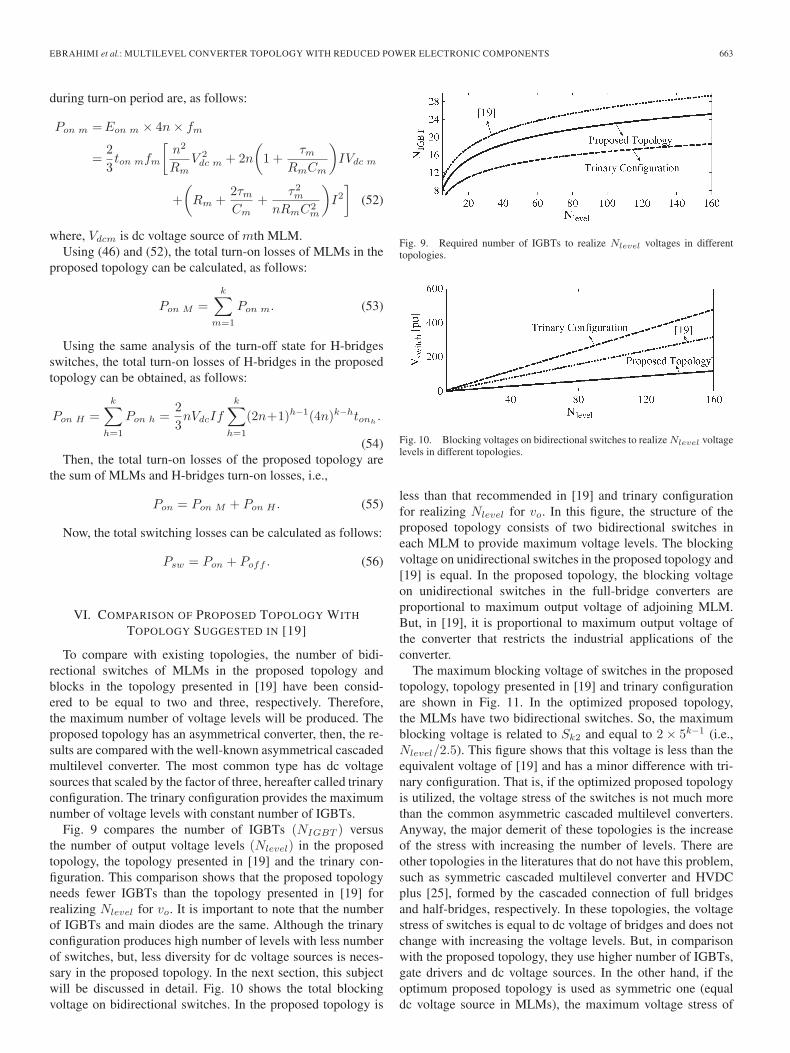
To compare with existing topologies, the number of bidi-rectional switches of MLMs in the proposed topology andblocks in the topology presented in [19] have been consid-ered to be equal to two and three, respectively. Therefore,the maximum number of voltage levels will be produced. Theproposed topology has an asymmetrical converter, then, the re-sults are compared with the well-known asymmetrical cascadedmultilevel converter. The most common type has dc voltagesources that scaled by the factor of three, hereafter called trinaryconfiguration. The trinary configuration provides the maximumnumber of voltage levels with constant number of IGBTs.
Fig. 9 compares the number of IGBTs (NIGBT ) versusthe number of output voltage levels (Nlevel) in the proposedtopology, the topology presented in [19] and the trinary con-figuration. This comparison shows that the proposed topologyneeds fewer IGBTs than the topology presented in [19] forrealizing Nlevel for vo. It is important to note that the numberof IGBTs and main diodes are the same. Although the trinaryconfiguration produces high number of levels with less numberof switches, but, less diversity for dc voltage sources is neces-sary in the proposed topology. In the next section, this subjectwill be discussed in detail. Fig. 10 shows the total blockingvoltage on bidirectional switches. In the proposed topology is
Fig. 9. Required number of IGBTs to realize Nlevel voltages in differenttopologies.
Fig. 10. Blocking voltages on bidirectional switches to realize Nlevel voltagelevels in different topologies.
less than that recommended in [19] and trinary configurationfor realizing Nlevel for vo. In this figure, the structure of theproposed topology consists of two bidirectional switches ineach MLM to provide maximum voltage levels. The blockingvoltage on unidirectional switches in the proposed topology and[19] is equal. In the proposed topology, the blocking voltageon unidirectional switches in the full-bridge converters areproportional to maximum output voltage of adjoining MLM.But, in [19], it is proportional to maximum output voltage ofthe converter that restricts the industrial applications of theconverter.
The maximum blocking voltage of switches in the proposedtopology, topology presented in [19] and trinary configurationare shown in Fig. 11. In the optimized proposed topology,the MLMs have two bidirectional switches. So, the maximumblocking voltage is related to Sk2 and equal to 2 × 5k−1 (i.e.,Nlevel/2.5). This figure shows that this voltage is less than theequivalent voltage of [19] and has a minor difference with tri-nary configuration. That is, if the optimized proposed topologyis utilized, the voltage stress of the switches is not much morethan the common asymmetric cascaded multilevel converters.Anyway, the major demerit of these topologies is the increaseof the stress with increasing the number of levels. There areother topologies in the literatures that do not have this problem,such as symmetric cascaded multilevel converter and HVDCplus [25], formed by the cascaded connection of full bridgesand half-bridges, respectively. In these topologies, the voltagestress of switches is equal to dc voltage of bridges and does notchange with increasing the voltage levels. But, in comparisonwith the proposed topology, they use higher number of IGBTs,gate drivers and dc voltage sources. In the other hand, if theoptimum proposed topology is used as symmetric one (equaldc voltage source in MLMs), the maximum voltage stress of

664 IEEE TRANSACTIONS ON INDUSTRIAL ELECTRONICS, VOL. 59, NO. 2, FEBRUARY 2012
Fig. 11. Maximum blocking voltage of switches for different Nlevel indifferent topologies.
Fig. 12. Required number of gate driver circuits to realize Nlevel voltagelevels in different topologies.
Fig. 13. Normalized conduction losses of switches versus Nlevel.
switches is equal to 2Vdc, that is, comparable with the commonsymmetric topologies.
Fig. 12 shows the required number of gate driver circuits forrealizing Nlevel of voltages for vo in the proposed topology,topology presented in [19] and trinary configuration. This figureshows that the proposed topology required less number of gatedriver circuits than [19] for Nlevel less than 20. For higherlevels, the number of gate driver circuits increases. But, it isnoticeable that the gate driver circuits are the electronic partof the circuit and has lower cost in comparison with powerelectronic components of the converter. Therefore, increasingthe number of gate driver circuits is not a considerable defi-ciency. The proposed topology not only has lower number ofswitches and components in comparison with [19], but also itsfull-bridge converters operate in the lower voltage. Considering(31), the overall peak value of the blocking voltage of full-bridge converters in the proposed topology and [19] are thesame, but in the topology presented in [19], this voltage isrelated to only one full-bridge converter.
Fig. 14. Normalized switching losses of switches versus Nlevel.
Figs. 13 and 14 show the normalized conduction and switch-ing losses, respectively, versus the number of output voltagelevels for the proposed topology and the topology presentedin [19]. To calculate the losses and possibility to compareproposed topology with other topology, it assumed that theswitches used in all MLM and H-bridges of two topologies arethe same. These comparisons show that the proposed topologyhas less conduction and switching losses than the others, espe-cially for higher number of voltage levels.
VII. DESIGN OF MULTILEVEL CONVERTER BASED ON
PROPOSED TOPOLOGY
In this section, a typical single-phase multilevel converterwith a minimum of 120 voltage levels and a peak value of400V should be designed. The on-state voltage drops of theswitches have been neglected. The optimal multilevel structureis presented in Fig. 15(a) for the minimum number of usedswitches. As shown in this figure, the number of IGBTs andcapacitors are 24 and 6, respectively. In this design, the numberof voltage levels is 125. The optimal structure based on theminimum number of capacitors is similar to Fig. 15(a). Theoptimal structure based on the minimum number of gate drivercircuits is shown in Fig. 15(b). In this structure, the numberof gate driver circuits is 21 and the number of voltage levelsis 343.
The structure of optimal multilevel with minimum usedswitches based on the recommended topology of [19] is pre-sented in Fig. 16(a). The number of IGBTs and capacitors are28 and 8, respectively, and the number of voltage levels is 161.The optimal multilevel structure with minimum used gate drivercircuits based on the topology presented in [19] is presented inFig. 16(b). The number of IGBTs and capacitors are 28 and6, respectively, and the number of voltage levels is 127. Thenumber of gate driver circuits is 16.
The design example by a trinary configuration of cas-caded multilevel inverter with five series-connected cells ispossible using 20 IGBTs. In this case, the number of volt-age levels is 243. In trinary configuration, five dc volt-age sources with different amplitudes should be used. But,three different dc voltage sources is need in the proposedtopology.
The blocking voltages of the bidirectional and unidirectionalswitches in Fig. 15(a) are 604.5 V and 806 V, respectively.These are 917.7 V and 786.6 V in Fig. 15(b). The blocking

EBRAHIMI et al.: MULTILEVEL CONVERTER TOPOLOGY WITH REDUCED POWER ELECTRONIC COMPONENTS 665
Fig. 15. Optimal multilevel structure with minimum used (a) switches (b) gatedriver circuits.
Fig. 16. Optimal multilevel structure with minimum (a) used switches and(b) gate driver circuits based on topology of [19].
voltages of the bidirectional and unidirectional switches inFig. 16(a) are 1000 V and 800 V, respectively. These are793.8 V and 793.8 V in Fig. 16(b).
VIII. EXPERIMENTAL RESULTS
To evaluate the performance of the proposed multilevelconverter in the generation of a desired output voltage wave-form, a single-phase 125-level multilevel converter prototypeis implemented based on the proposed topology shown inFig. 15(a). The IGBTs are BUP306D with internal anti-paralleldiodes. The 89C52 microcontroller of ATMEL Company hasbeen used to generate the switching patterns. The required dcvoltage sources have been provided by cascaded connection ofdc power supplies. There are several modulation techniques formultilevel converters [26]–[30]. In this paper, the fundamental
Fig. 17. Experimental results; (a) output voltage of first full-bridge (vo1);(b) output voltage of second full-bridge (vo2); (c) output voltage of third full-bridge (vo3); (d) converter output voltage (vo); and (e) converter current.
frequency switching technique has been used. The main objectof the control strategy is to synthesis the output voltage thatminimizes the error with respect to the reference voltage. Itis important to note that the calculation of optimal switchingangles for the elimination of the selected harmonics or theminimization of the total harmonic distortion (THD) is not theobjective of this work.
In the experimental case, the waveforms of the output volt-ages, produced by different full-bridges, and the output currenthave been studied. In this regard, the converter has been ad-justed to produce a 50 Hz, 13-level staircase waveform. In thistest, the load is a series R-L load (R = 20 Ω and L = 55 mH).The result of this test is shown in Fig. 17. As shown in thisfigure, the ac output of each full-bridge is connected in seriessuch that the synthesized voltage waveform is the sum of theoutputs of the full-bridge. Considering the output voltage and

666 IEEE TRANSACTIONS ON INDUSTRIAL ELECTRONICS, VOL. 59, NO. 2, FEBRUARY 2012
current waveforms, it is obvious that there is a phase differencebetween voltage and current waveforms, due to the inductivebehavior of the load. The Fourier series expansion of thestepped output voltage waveform of the multilevel converter,as shown in Fig. 17(d), have a fundamental frequency and aninfinite number of odd harmonics [28]. It can be seen thatthe output current is almost sinusoidal. Since the load of theconverter (R-L) behaves as a low-pass filter. In this case, theTHDs of the output voltage and current based on simulationresults (using PSCAD/EMTDC software) are %5.9 and %0.64,respectively. To generate a desired output with best qualityof the waveform, the number of the voltage steps should beincreased or another appropriate switching technique should beused.
IX. CONCLUSION
A new basic multilevel module (MLM) for the multilevelconverter has been proposed. The proposed topology is a com-bination of MLMs and full-bridges converter. The proposedtopology extends the design flexibility and the possibilitiesto optimize the converter for various objectives. It has beenshown that the structure, consisting of MLMs with two switcheshas the minimum number of switches for a given number ofvoltage levels. The proposed topology has been compared withother topology. It has been shown that the proposed topologyprovides 125 levels on the output voltage with a peak of400 V, using 24 IGBTs and the blocking voltage of 604.5 Von bidirectional switches. But, the other topology produces161 voltage levels using 28 IGBTs and a blocking voltage of1000 V. The proposed topology not only has lower switchesand components in comparison with other one, but also its full-bridge converters operate in the lower voltage. The operationand performance of the proposed topology has been experimen-tally verified on a single-phase 125-level multilevel converterprototype. Reduction of the power losses of the proposedtopology in comparison other topology is another advantageof the proposed converter. The proposed topology can be agood solution for applications that require high power quality,or applications that have considerable numbers of dc voltagesources.
REFERENCES
[1] J. Rodriguez, B. Wu, S. Bernet, J. Pontt, and S. Kouro, “Multilevel voltagesource converter topologies for industrial medium voltage drives,” IEEETrans. Ind. Electron., vol. 54, no. 6, pp. 2930–2945, Dec. 2007.
[2] H. Abu-Rub, J. Holtz, J. Rodriguez, and G. Baoming, “Medium voltagemultilevel converters—State of the art, challenges and requirements in in-dustrial applications,” IEEE Trans. Ind. Electron, vol. 57, no. 8, pp. 2581–2596, Aug. 2010.
[3] E. Babaei and S. H. Hosseini, “New cascaded multilevel inverter topologywith minimum number of switches,” J. Energy Convers. Manag., vol. 50,no. 11, pp. 2761–2767, Nov. 2009.
[4] E. Babaei and M. S. Moeinian, “Asymmetric cascaded multilevel inverterwith charge balance control of a low resolution symmetric subsystem,”J. Energy Convers. Manag., vol. 51, no. 11, pp. 2272–2278, Nov. 2010.
[5] A. Nabae, I. Takahashi, and H. Akagi, “A new neutral-point-clampedPWM inverter,” IEEE Trans. Ind. Appl., vol. IA-17, no. 5, pp. 518–523,Sep. 1981.
[6] T. A. Meynard and H. Foch, “Multi-level choppers for high voltageapplications,” in Proc. Eur. Conf. Power Electron. Appl., 1992, vol. 2,pp. 45–50.
[7] M. Marchesoni, M. Mazzucchelli, and S. Tenconi, “A non conventionalpower converter for plasma stabilization,” in Proc. Power Electron. Spec.Conf., 1988, pp. 122–129.
[8] S. S. Fazel, S. Bernet, D. Krug, and K. Jalili, “Design and compari-son of 4-kV neutral-point-clamped, flying-capacitor, and series-connectedH-bridge multilevel converters,” IEEE Trans. Ind. Appl., vol. 43, no. 4,pp. 1032–1040, Jul./Aug. 2007.
[9] B. P. McGrath and D. G. Holmes, “Analytical modelling of voltage bal-ance dynamics for a flying capacitor multilevel converter,” IEEE Trans.Power Electron., vol. 23, no. 2, pp. 543–550, Mar. 2008.
[10] P. Lezana, J. Pou, T. A. Meynard, J. Rodriguez, S. Ceballos, andF. Richardeau, “Survey on fault operation on multilevel invert-ers,” IEEE Trans. Ind. Electron, vol. 57, no. 7, pp. 2207–2218,Jul. 2010.
[11] A. K. Sadigh, S. H. Hosseini, M. Sabahi, and G. B. Gharehpetian, “Dou-ble flying capacitor multicell converter based on modified phase-shiftedpulsewidth modulation,” IEEE Trans. Power Electron., vol. 25, no. 6,pp. 1517–1526, Jun. 2010.
[12] C. Rech and J. R. Pinheiro, “Hybrid multilevel converters: Unified analy-sis and design considerations,” IEEE Trans. Ind. Electron., vol. 54, no. 2,pp. 1092–1104, Apr. 2007.
[13] C. Rech and J. R. Pinheiro, “Line current harmonics reduction in multi-pulse connection of asymmetrically loaded rectifiers,” IEEE Trans. Ind.Electron., vol. 52, no. 3, pp. 640–652, Jun. 2005.
[14] S. Lu, S. Marieethoz, and K. A. Corzine, “Asymmetrical cascade mul-tilevel converters with noninteger or dynamically changing dc voltageratios: Concepts and modulation techniques,” IEEE Trans. Ind. Electron.,vol. 57, no. 7, pp. 2411–2418, Jul. 2010.
[15] J. Rodriguez, L. G. Franquelo, S. Kouro, J. I. Leon, R. C. Portillo,M. A. M. Prats, and M. A. Perez, “Multilevel converters: An enablingtechnology for high-power applications,” Proc. IEEE, vol. 97, no. 11,pp. 1786–1817, Nov. 2009.
[16] M. Malinowski, K. Gopakumar, J. Rodriguez, and M. Perez, “A survey oncascaded multilevel inverters,” IEEE Trans. Ind. Electron., vol. 57, no. 7,pp. 2197–2206, Jul. 2010.
[17] M. T. Haque, “Series sub-multilevel voltage source inverters (MLVSIs) asa high quality MLVSI,” in Proc. SPEEDAM, 2004, pp. F1B-1–F1B-4.
[18] E. Babaei, S. H. Hosseini, G. B. Gharehpetian, M. T. Haque, andM. Sabahi, “Reduction of DC voltage sources and switches in asymmet-rical multilevel converters using a novel topology,” J. Elect. Power Syst.Res., vol. 77, no. 8, pp. 1073–1085, Jun. 2007.
[19] E. Babaei, “A cascade multilevel converter topology with reduced numberof switches,” IEEE Trans. Power Electron., vol. 23, no. 6, pp. 2657–2664,Nov. 2008.
[20] G. Su, “Multilevel dc-link inverter,” IEEE Trans. Ind. Appl., vol. 41, no. 3,pp. 848–854, May/Jun. 2005.
[21] P. Lezana and J. Rodriguez, “Mixed multicell cascaded multilevel in-verter,” in Proc. ISIE, 2007, pp. 509–514.
[22] S. Rohner, S. Bernet, M. Hiller, and R. Sommer, “Modulation,losses, and semiconductor requirements of modular multilevel con-verters,” IEEE Trans. Ind. Electron., vol. 57, no. 8, pp. 2633–2642,Aug. 2010.
[23] T. J. Kim, D. W. Kang, Y. H. Lee, and D. S. Hyun, “The analysis ofconduction and switching losses in multi-level inverter system,” in Proc.Power Eletron. Spec. Conf., 2001, pp. 1363–1368.
[24] S. Sunter and H. Altun, “A method for calculating semiconductor lossesin the matrix converter,” in Proc. MELECON, 1998, pp. 1260–1264.
[25] K. Friedrich, “Modern HVDC PLUS application of VSC in modularmultilevel converter topology,” in Proc. ISIE, 2010, pp. 3807–3810.
[26] Y. Liu, H. Hong, and A. Q. Huang, “Real-time algorithm for minimiz-ing THD in multilevel inverters with unequal or varying voltage stepsunder staircase modulation,” IEEE Trans. Ind. Electron., vol. 56, no. 6,pp. 2249–2258, Jun. 2009.
[27] J. I. Leon, S. Vazquez, S. Kouro, L. G. Franquelo, J. M. Carrasco, andJ. Rodriguez, “Unidimensional modulation technique for cascaded mul-tilevel converters,” IEEE Trans. Ind. Electron., vol. 56, no. 8, pp. 2981–2986, Aug. 2009.
[28] P. Cortes, A. Wilson, S. Kouro, J. Rodriguez, and H. Abu-Rub, “Modelpredictive control of multilevel cascaded H-bridge inverters,” IEEE Trans.Ind. Electron., vol. 57, no. 8, pp. 2691–2699, Aug. 2010.
[29] E. Villanueva, P. Correa, J. Rodriguez, and M. Pacas, “Control of a single-phase cascaded H-bridge multilevel inverter for grid-connected photo-voltaic systems,” IEEE Trans. Ind. Electron., vol. 56, no. 11, pp. 4399–4406, Nov. 2009.
[30] D. C. Ludois, J. K. Reed, and G. Venkataramanan, “Hierarchical controlof bridge-of-bridge multilevel power converters,” IEEE Trans. Ind. Elec-tron., vol. 57, no. 8, pp. 2679–2690, Aug. 2010.

EBRAHIMI et al.: MULTILEVEL CONVERTER TOPOLOGY WITH REDUCED POWER ELECTRONIC COMPONENTS 667
Javad Ebrahimi (S’10) was born in Isfahan, Iran,in 1986. He received the B.Sc. degree in electricalengineering from University of Tabriz, Tabriz, Iran,in 2008, and the M.S. degree in electrical engineeringfrom Amirkabir University of Technology (AUT),Tehran, Iran, in 2010, graduating with First ClassHonors, where he is currently working toward thePh.D. degree at Electrical Engineering Department.
His current research interests include the analysisand control of power electronic converters, multi-level converters, FACTS devices, and Distributed
Generation.
Ebrahim Babaei (M’10) was born in Ahar, Iran, in1970. He received the B.S. degree in electronic engi-neering and the M.S. degree in electrical engineer-ing from the Department of Engineering, Universityof Tabriz, Tabriz, Iran, in 1992 and 2001, respec-tively, graduating with first class honors. He receivedthe Ph.D. degree in electrical engineering from theDepartment of Electrical and Computer Engineering,University of Tabriz, in 2007.
In 2004, he joined the Faculty of Electrical andComputer Engineering, University of Tabriz. He was
an Assistant Professor in University of Tabriz from 2007 to 2011 and has beenan Associate Professor since 2011. He is the author of more than 100 journaland conference papers. His current research interests include the analysisand control of power electronic converters, matrix converters and multilevelconverters, FACTS devices and power system dynamics.
Gevorg B. Gharehpetian (M’00–SM’08) was bornin Tehran, Iran, in 1962. He received the B.S. de-gree in electrical engineering from Tabriz University,Tabriz, Iran, in 1987, the M.S. degree in electricalengineering from Amirkabir University of Technol-ogy (AUT), Tehran, Iran, in 1989, graduating withFirst Class Honors, and the Ph.D. degree in electricalengineering from Tehran University, Tehran, Iran, in1996. As a Ph.D. student, he has received scholarshipfrom DAAD (German Academic Exchange Service)from 1993 to 1996 and he was with High Voltage
Institute of RWTH Aachen, Aachen, Germany.In 1989, he joined the Electrical Engineering Department of AUT as a
lecturer. He has been holding the Assistant Professor position in AUT from1997 to 2003, the position of Associate Professor from 2004 to 2007, andhas been Professor since 2007. In 2008, he was selected by the ministry ofhigher education as the distinguished professor of Iran and was awarded theNational Prize. He is the author of more than 400 journal and conference papers.His teaching and research interest include power system and transformerstransients, FACTS devices, and HVDC transmission.