3006 IEEE JOURNAL OF SOLID-STATE CIRCUITS, VOL. 52, NO. 11 ...
12
3006 IEEE JOURNAL OF SOLID-STATE CIRCUITS, VOL. 52, NO. 11, NOVEMBER 2017 A Low-Power CMOS Crystal Oscillator Using a Stacked-Amplifier Architecture Shunta Iguchi, Member, IEEE, Takayasu Sakurai, Fellow, IEEE , and Makoto Takamiya, Senior Member, IEEE Abstract— This paper presents a low-power 39.25-MHz crystal oscillator with a new stacked-amplifier architecture achieving the smallest figure of merit (FoM) ever reported for a crystal oscillator for wireless communications. Theoretical analyses of the power consumption and the phase noise (PN) in the proposed stacked-amplifier architecture are newly provided to clarify the reason why the proposed stacked-amplifier architecture achieves the smallest FoM. Additionally, a new self-forward-body-biasing technique and flicker noise suppression technique are shown to reduce the minimum operational supply voltage (V DD(MIN) ) and the PN, respectively. The proposed 3.3-V, 39.25-MHz stacked- amplifier crystal oscillator fabricated in a 65-nm CMOS process exhibits the smallest FoM for a crystal oscillator of -248 dBc/Hz with a power consumption of 19 μW and PN of -139 dBc/Hz at 1-kHz offset frequency. The relative frequency errors among 11 samples at temperatures of -30 °C to 80 °C and for ±10% supply voltage variation are ±10.5 ppm and ±0.12 ppm, respectively. The long-term frequency error is -0.98 ppm in the first year (=365 days). Index Terms—CMOS, crystal oscillator, low noise, low power, quartz crystal, stacked-amplifier architecture. I. I NTRODUCTION C RYSTAL oscillators have undergone revolutionary decades every 30–40 years since their invention by Nicolson [1] and Cady [2] in the 1920s. Many technical challenges to reduce the aging effect [3] around World War II in the 1940s–50s and to achieve low-power operation for wristwatches in the 1970s–80s [4], [5] were overcome owing to the huge demand for crystal oscillators. In the 2020s, the Internet of Things (IoT) [6] is a promising application to provide the huge demand for crystal oscillators because it requires a huge capacity for wireless communications. The low-power and low-noise operation of crystal oscillators is the most fundamental requirement for energy-efficient wireless communications (e.g., Bluetooth with low energy (BLE) [7]) in IoT applications. The tradeoff between the power con- sumption ( P dc ) 1 and the single-sideband phase noise (PN) in oscillator circuits can be evaluated using the following figure of merit (FoM) [8] with the unit of dBc/Hz: FoM = PN − 20 log 10 ( f OSC / f OFFSET ) + 10 log 10 ( P dc ) (1) Manuscript received February 17, 2017; revised April 30, 2017 and June 24, 2017; accepted August 14, 2017. Date of publication September 13, 2017; date of current version October 23, 2017. This work was partly supported by STARC. This paper was approved by Associate Editor Seonghwan Cho. (Corresponding author: Shunta Iguchi.) The authors are with The University of Tokyo, Tokyo 153-8505, Japan (e-mail: [email protected]). Color versions of one or more of the figures in this paper are available online at http://ieeexplore.ieee.org. Digital Object Identifier 10.1109/JSSC.2017.2743174 1 Note that P dc in (1) must be calculated in the unit of milliwatt for consistency with the unit of dBc/Hz in (1). where f OSC is the oscillation frequency, f OFFSET is the offset frequency from f OSC , and the unit of PN is dBc/Hz. For the low-power and low-noise operation of oscillator circuits, circuit designers should aim to achieve a smaller FoM than that in conventional studies. This paper reports a low-power and low-noise crystal oscillator with the smallest FoM ever reported for a crystal oscillator. In Section II, the concept of a stacked-amplifier architecture [9] and theoretical analyses of P dc and PN in the stacked-amplifier architecture are newly presented to clarify its advantages for reducing FoM, thereby demonstrating the low-power and low-noise operation of the crystal oscillator. In Section III, the detailed circuit designs with the stacked- amplifier architecture are shown. Additionally, a new self- forward-body-biasing technique and flicker noise suppression technique are demonstrated that, respectively, reduce P dc and PN for the proposed crystal oscillator. To verify the low-power, low-noise, and reliable operation of the proposed crystal oscillator, measurement results are given in Section IV. Finally, conclusions are given in Section V. II. ANALYSIS OF STACKED-AMPLIFIER ARCHITECTURE To clarify the advantages of the stacked-amplifier archi- tecture for achieving low-power and low-noise operation, theoretical analyses of P dc and PN are newly presented in this section. The analyses clarify the reason why the stacked- amplifier architecture can achieve the smallest FoM. A. Power Reduction With Stacked-Amplifier Architecture The power consumption in many crystal oscillator architectures [5], [10]–[16] is mainly determined by a negative resistance generator consisting of an amplifier circuit (e.g., an inverter amplifier and differential amplifier). Several techniques using an energy-efficient amplifier operating in the weak-inversion region (overdrive voltage: V OV < 0) [5], [16], an intermittent amplifier [17], [18], and a pulsed driver [19], [20] have been reported for achieving low-power operation. However, these conventional techniques targeted a low-frequency (e.g., 32.768 kHz) real-time-clock (RTC) generator because PN in an RTC does not make significant problems as a system clock. The temperature dependence and aging effect of the oscillation frequency are the major problems in such applications. On the other hand, high-frequency (>10 MHz) crystal oscillators for wireless communications require a low PN because the PN in a crystal oscillator and phase-locked loop (PLL) 2 degrades the 2 The PN in the crystal oscillator is amplified by the frequency multiplication ratio in the PLL. In a case of upconversion from 24 MHz to 2.4 GHz, the PN in the PLL is 40 dB (=20 × log 10 (100)) larger than that in the crystal oscillator. 0018-9200 © 2017 IEEE. Personal use is permitted, but republication/redistribution requires IEEE permission. See http://www.ieee.org/publications_standards/publications/rights/index.html for more information.
Transcript of 3006 IEEE JOURNAL OF SOLID-STATE CIRCUITS, VOL. 52, NO. 11 ...

3006 IEEE JOURNAL OF SOLID-STATE CIRCUITS, VOL. 52, NO. 11, NOVEMBER 2017
A Low-Power CMOS Crystal Oscillator Usinga Stacked-Amplifier Architecture
Shunta Iguchi, Member, IEEE, Takayasu Sakurai, Fellow, IEEE, and Makoto Takamiya, Senior Member, IEEE
Abstract— This paper presents a low-power 39.25-MHz crystaloscillator with a new stacked-amplifier architecture achievingthe smallest figure of merit (FoM) ever reported for a crystaloscillator for wireless communications. Theoretical analyses ofthe power consumption and the phase noise (PN) in the proposedstacked-amplifier architecture are newly provided to clarify thereason why the proposed stacked-amplifier architecture achievesthe smallest FoM. Additionally, a new self-forward-body-biasingtechnique and flicker noise suppression technique are shown toreduce the minimum operational supply voltage (VDD(MIN)) andthe PN, respectively. The proposed 3.3-V, 39.25-MHz stacked-amplifier crystal oscillator fabricated in a 65-nm CMOS processexhibits the smallest FoM for a crystal oscillator of −248 dBc/Hzwith a power consumption of 19 µW and PN of −139 dBc/Hzat 1-kHz offset frequency. The relative frequency errors among11 samples at temperatures of −30 °C to 80 °C and for±10% supply voltage variation are ±10.5 ppm and ±0.12 ppm,respectively. The long-term frequency error is −0.98 ppm in thefirst year (=365 days).
Index Terms— CMOS, crystal oscillator, low noise, low power,quartz crystal, stacked-amplifier architecture.
I. INTRODUCTION
CRYSTAL oscillators have undergone revolutionarydecades every 30–40 years since their invention by
Nicolson [1] and Cady [2] in the 1920s. Many technicalchallenges to reduce the aging effect [3] around World War IIin the 1940s–50s and to achieve low-power operation forwristwatches in the 1970s–80s [4], [5] were overcome owingto the huge demand for crystal oscillators. In the 2020s,the Internet of Things (IoT) [6] is a promising applicationto provide the huge demand for crystal oscillators because itrequires a huge capacity for wireless communications. Thelow-power and low-noise operation of crystal oscillators isthe most fundamental requirement for energy-efficient wirelesscommunications (e.g., Bluetooth with low energy (BLE) [7])in IoT applications. The tradeoff between the power con-sumption (Pdc)1 and the single-sideband phase noise (PN)in oscillator circuits can be evaluated using the followingfigure of merit (FoM) [8] with the unit of dBc/Hz:FoM = PN − 20 log10( fOSC/ fOFFSET) + 10 log10(Pdc) (1)
Manuscript received February 17, 2017; revised April 30, 2017 andJune 24, 2017; accepted August 14, 2017. Date of publicationSeptember 13, 2017; date of current version October 23, 2017. This workwas partly supported by STARC. This paper was approved by AssociateEditor Seonghwan Cho. (Corresponding author: Shunta Iguchi.)
The authors are with The University of Tokyo, Tokyo 153-8505, Japan(e-mail: [email protected]).
Color versions of one or more of the figures in this paper are availableonline at http://ieeexplore.ieee.org.
Digital Object Identifier 10.1109/JSSC.2017.27431741Note that Pdc in (1) must be calculated in the unit of milliwatt for
consistency with the unit of dBc/Hz in (1).
where fOSC is the oscillation frequency, fOFFSET is the offsetfrequency from fOSC, and the unit of PN is dBc/Hz. Forthe low-power and low-noise operation of oscillator circuits,circuit designers should aim to achieve a smaller FoM thanthat in conventional studies.
This paper reports a low-power and low-noise crystaloscillator with the smallest FoM ever reported for a crystaloscillator. In Section II, the concept of a stacked-amplifierarchitecture [9] and theoretical analyses of Pdc and PN in thestacked-amplifier architecture are newly presented to clarifyits advantages for reducing FoM, thereby demonstrating thelow-power and low-noise operation of the crystal oscillator.In Section III, the detailed circuit designs with the stacked-amplifier architecture are shown. Additionally, a new self-forward-body-biasing technique and flicker noise suppressiontechnique are demonstrated that, respectively, reduce Pdc andPN for the proposed crystal oscillator. To verify the low-power,low-noise, and reliable operation of the proposed crystaloscillator, measurement results are given in Section IV. Finally,conclusions are given in Section V.
II. ANALYSIS OF STACKED-AMPLIFIER ARCHITECTURE
To clarify the advantages of the stacked-amplifier archi-tecture for achieving low-power and low-noise operation,theoretical analyses of Pdc and PN are newly presented inthis section. The analyses clarify the reason why the stacked-amplifier architecture can achieve the smallest FoM.
A. Power Reduction With Stacked-Amplifier Architecture
The power consumption in many crystal oscillatorarchitectures [5], [10]–[16] is mainly determined by anegative resistance generator consisting of an amplifier circuit(e.g., an inverter amplifier and differential amplifier). Severaltechniques using an energy-efficient amplifier operating in theweak-inversion region (overdrive voltage: VOV < 0) [5], [16],an intermittent amplifier [17], [18], and a pulseddriver [19], [20] have been reported for achieving low-poweroperation. However, these conventional techniques targeteda low-frequency (e.g., 32.768 kHz) real-time-clock (RTC)generator because PN in an RTC does not make significantproblems as a system clock. The temperature dependenceand aging effect of the oscillation frequency are themajor problems in such applications. On the other hand,high-frequency (>10 MHz) crystal oscillators for wirelesscommunications require a low PN because the PN in acrystal oscillator and phase-locked loop (PLL)2 degrades the
2The PN in the crystal oscillator is amplified by the frequency multiplicationratio in the PLL. In a case of upconversion from 24 MHz to 2.4 GHz, the PN inthe PLL is 40 dB (=20× log10(100)) larger than that in the crystal oscillator.
0018-9200 © 2017 IEEE. Personal use is permitted, but republication/redistribution requires IEEE permission.See http://www.ieee.org/publications_standards/publications/rights/index.html for more information.

IGUCHI et al.: LOW-POWER CMOS CRYSTAL OSCILLATOR USING STACKED-AMPLIFIER ARCHITECTURE 3007
Fig. 1. Schematics of (a) conventional one-stage CMOS Pierce crystal oscillator, (b) proposed stacked-amplifier crystal oscillator, (c) equivalent circuit ofthe quartz crystal, and (d) table comparing properties of a conventional oscillator and the proposed oscillator.
sensitivity of wireless receivers owing to adjacent-channelinterference.
To achieve low-power and low-noise operation, the stacked-amplifier architecture was proposed in [9]. Fig. 1(a)–(d) showsthe schematics of a conventional one-stage CMOS Pierce crys-tal oscillator, a proposed stacked-amplifier crystal oscillatorwith N-stages stacked amplifiers, an equivalent circuit of thequartz crystal, and a table comparing the properties of a con-ventional oscillator and the proposed oscillator, respectively.C1 is the gate-to-ground capacitor, C2 is the drain-to-groundcapacitor, C3 is the parallel parasitic capacitor in the quartzcrystal, and R3 is the feedback resistor. CM, LM, and RMare the motional capacitor, inductor, and resistor in the quartzcrystal, respectively. The current waveform (IM) in the nodecontaining CM, LM, and RM is expressed as |IM| × cos(ωt),where |IM| is the amplitude of the current swing, ω is theangular frequency, and t is the time. The inverter amplifiersin Fig. 1(a) and (b) configure the negative resistance (RN) toprovide energy to the resonator of the quartz crystal. In manycases, the amplifiers are biased by a current source with abias current (ID) to reduce the sensitivity to process, voltage,and temperature (PVT) variations. The inverter amplifiersexcept for that in the lowest stage (N = 1) in Fig. 1(b)consist of a CMOS inverter, a decoupling capacitor (CD), andtwo coupling capacitors at the gate (CCG) and drain (CCD).
|V1| and |V2| are the amplitudes of the voltage swing at thegate and drain of the inverter amplifier, respectively. Assumingthat C1 = C2 and gm(TOTAL) � ωOSC for simplicity, the equiv-alent RN [5], [21] in Fig. 1(a) and (b) is approximated as
RN = − gm(TOTAL)C1C2
g2m(TOTAL)C
23 + ω2
OSC(C1C2 + C2C3 + C3C1)2
≈ − gm(TOTAL)
ω2OSC(C1 + 2C3)2
(2)
where gm(TOTAL) is the equivalent transconductance of theinverter amplifiers and ωOSC is the angular frequency of fOSC.In the initial state, the absolute value of RN (|RN|) is set toapproximately five times larger than RM to ensure reliableand quick startup [22]. In the steady state, |RN| settles downto RM owing to the nonlinearity of the amplifiers. Thisindicates that the characteristic of the quartz crystal (=RM)is the fundamental limitation in minimizing the value ofgm(TOTAL) and the corresponding power consumption of thecrystal oscillators. In Fig. 1(a), gm(TOTAL) is simply given bythe transconductance (gm0) in an inverter amplifier. On theother hand, gm(TOTAL) in Fig. 1(b) is given by
gm(TOTAL) =N∑
i=1
gmi = gm1 + gm2 + · · · + gmN (3)

3008 IEEE JOURNAL OF SOLID-STATE CIRCUITS, VOL. 52, NO. 11, NOVEMBER 2017
where gmN is the transconductance of the inverter ampli-fiers in the N th stage. When the impedances of CD, CCG,and CCD are approximated to zero at fOSC, the stackedamplifiers in Fig. 1(b) are equivalent to a transconductanceamplifier with a transconductance of gm(TOTAL), because allthe stacked amplifiers are virtually connected in parallelat fOSC. The minimum transconductance of each inverteramplifier in the proposed stacked-amplifier crystal oscillatoris N times smaller than that of the conventional one-stageCMOS Pierce crystal oscillator. The smaller transconductancein the proposed architecture makes it possible to reducePdc compared with that of conventional crystal oscillators.This discussion is summarized in Fig. 1(d), which clarifiesthe difference between the conventional architecture and theproposed stacked-amplifier architecture.
Subsequently, the power consumption of the stacked-amplifier crystal oscillator is analytically derived using ideallong-channel models [23] to verify the power reduction by theproposed architecture. The theoretical analyses are performedusing fixed-size amplifiers because the aim of this paper is todesign a low-power crystal oscillator for low-energy wirelesscommunications (e.g., BLE). Such low-power operation isa more essential requirement than small-area implementa-tion for this application. For simplicity, it is assumed thatthe transconductances (gmN and gmP) and threshold voltages(VTHN and VTHP) of the NMOS and PMOS transistors arethe same without random variations. The lengths of theNMOS (LN) and PMOS (LP) transistors are the same, andtheir widths (WN and WP) are varied as n × WN = WP tosatisfy the condition gmN = gmP, where n is the relative sizeratio of WP compared with WN.
When the sizes of the inverter amplifiers in each stageare fixed for the stacked-amplifier architecture with N-stagesstacked amplifiers, VOV is scaled down by a factor of N . Then,the relationship between gmN, gmP, gm(TOTAL), ID, and N isgiven as
gmN = gmP = gm(TOTAL)
2N= √
2μNCOX(WN/LN)ID (4)
where μN is the carrier mobility in the NMOS transistor andCOX is the unit capacitance of the gate oxide. Substituting (4)into (2), ID in the case of N-stages stacked amplifiers isderived as
ID = ω4OSC|RN|2(C1 + 2C3)
4
8N2μNCOX(WN/LN)∝ 1
N2 . (5)
Equation (5) clarifies that ID and Pdc are proportional to 1/N2.The power consumption of the proposed stacked-amplifierarchitecture is 16 times smaller than that of the conventionalone-stage CMOS Pierce crystal oscillator when four-stagestacked amplifiers are available. To verify the consistency ofthe derived equation, the simulated N dependence of ID isshown in Fig. 2. The simulated results show that the poweris reduced by a factor of N2 within a relative error of 42%.The simulated ID is reduced by 91% from 65.4 μA (N = 1)to 5.8 μA (N = 4). It is verified that the proposed stacked-amplifier architecture can reduce Pdc by increasing N . Notethat the maximum value of N is limited by the minimum
Fig. 2. Simulated N dependence of ID at |RN| of 50 �. The solid lineshows a function of 1/N2 fit using the value of ID at N = 1 to verify theconsistency of the proportional relationship with the factor of 1/N2.
operational supply voltage (VDD(MIN)) and the design specifi-cation for PVT variations.
VDD(MIN) in the stacked-amplifier architecture is higher thanthat in the conventional one-stage Pierce crystal oscillator;however, the higher VDD(MIN) is not a critical problem inmany cases because crystal oscillators are often powered byI/O voltage (e.g., 3.3 V). There are several reasons why crystaloscillators utilize I/O voltage. Firstly, crystal oscillators needto start up first and provide the clock for all sub-blocks ina system-on-chip (SoC). Second, crystal oscillators are oftendesigned as an I/O cell for small-area implementation withelectrostatic discharge protection circuits and I/O pads. Third,the power supply of a crystal oscillator should be isolatedfrom the core supply voltage because the harmonics of theoscillation frequency in the crystal oscillator propagate tonoise-sensitive circuits (e.g., wireless receivers) through thepower supply.
In contrast, the maximum voltage swing in a crystal oscil-lator should be smaller than a certain voltage (e.g., 0.8 V) tominimize the long-term frequency variation (e.g., 1 ppm/year).The large difference between the supply voltage and oscillationamplitude (e.g., 3.3 V − 0.8 V = 2.5 V) is the fundamentallimitation in reducing the power consumption. This largevoltage difference has been decreased by employing a resistivedivider consisting of a low-dropout (LDO) regulator and a cur-rent source in conventional approaches [13], [16]. The powerloss in the resistive divider is not negligible in low-powerapplications. On the other hand, dc–dc converters (e.g., Buckconverters) are not available for low-noise crystal oscillatordesigns because the output noise in a dc–dc converter is signif-icantly larger than that in an LDO. Additionally, the overheadsof the area and cost of a capacitor, inductor, and I/O pads arenot feasible for low-cost IoT applications. The advantage ofthe proposed stacked-amplifier architecture is that it utilizesthe wasted voltage drop to increase gm(TOTAL). The proposedarchitecture reduces the total power consumption, includingthe voltage drop in the LDO and current source, comparedwith conventional approaches using one-stage Pierce crystaloscillators.
B. Phase Noise in Stacked-Amplifier Architecture
The FoM in oscillator circuits is calculated from Pdc andPN using (1). A detailed analysis of the noise in the proposedstacked-amplifier architecture is also important to clarify its

IGUCHI et al.: LOW-POWER CMOS CRYSTAL OSCILLATOR USING STACKED-AMPLIFIER ARCHITECTURE 3009
advantages compared with conventional architectures. In crys-tal oscillator design, PN for fOFFSET of 1–10 kHz should bereduced to as low as possible because it is difficult to suppressPN in this frequency range by using a loop filter in a PLL. Thissection provides a theoretical analysis of the PN due to flickernoise because the contribution of flicker noise is considerablylarger than that of thermal noise in this frequency range. TheN dependence of PN is analytically discussed using lineartime-varying (LTV) theory [24], [25].
The spectrum of PN at a low fOFFSET (=1/ f 3 region)is mainly determined by the flicker noise in transistorsand the upconversion effect due to the impulse response inLTV systems. In accordance with LTV theory and a theoreticalanalysis [26], PN for a Pierce crystal oscillator in the 1/ f 3
region (PN1/f3) is given as
P N 1/f3 = �2dc I 2
D_n(rms)
2(C2|V2|)2ω2OFFSET
(CM
C2
)2
(6)
where �dc is the direct current (dc) value of the effec-tive impulse sensitivity function for a sinusoidal voltage of|V2| × sin(ωt) and ID_n(rms) is the root-mean-square (RMS)value of the noise current in ID for a 1-Hz bandwidth.The angular frequency of fOFFSET is denoted as ωOFFSET.Equation (6) can be applied3 to all types of Pierce crys-tal oscillator including the one-stage CMOS Pierce crystaloscillator and the stacked-amplifier crystal oscillator shownin Fig. 1. ID_n(rms) is one of a few controllable parameters forcircuit designers. PN in the 1/ f 3 region should be reduced byensuring a small ID_n(rms).
To analyze the N dependence of PN in the 1/ f 3 region;at first, ID_n(rms) for different numbers of stacked amplifiersis derived because ID_n(rms) can easily be calculated using asmall-signal approximation. According to [26], the square ofthe equivalent flicker noise voltage (V 2
1/f_n(rms)) at the gate ofa transistor is given as
V 21/f_n(rms) = K
ωLW(7)
where K is the flicker noise voltage constant, L and Ware the length and width of the transistors, respectively.In the following discussion, the values of K in NMOS andPMOS transistors are denoted as KN and KP, respectively.I 2D_n(rms) with the N-stages stacked amplifiers is derived
as
I 2D_n(rms) = (nKN + KP)g2
m(TOTAL)
16nωN3 LNWN∝ 1
N3 . (8)
The detailed derivation of (8) is given in the Appendix.Equation (8) clarifies that I 2
D_n(rms) is reduced by a factor ofN3 when N-stages stacked amplifiers are used for the pro-posed stacked-amplifier architecture. A comparison betweena theoretical calculation using (8) and simulation results isshown in Fig. 3. The calculated results match to the simulationresults within a relative error of 21%. The small error verifiesthat (8) is consistent with the simulation results. For the
3Note that the theoretical calculation of �dc is complicated even in theideal case assuming sinusoidal voltage waveforms. For simplicity, this studyassumes that �dc is independent of N .
Fig. 3. Simulated frequency dependences of I 2D_n(rms) with |RN| of 50 �
at N = 1, 2, 3, and 4. Solid lines show the results calculated using (8). Thesimulated and calculated results verify that the flicker noise in ID is inverselyproportional to N3.
calculations using (8), KN and KP are extracted by SPICEsimulation because they depend on the overdrive voltage ofthe transistors [27]. The N dependences of KN and KP arenot incorporated in (8) for simplicity. It is concluded that theproposed stacked-amplifier architecture can reduce both Pdcand I 2
D_n(rms) in the 1/ f 3 region by increasing N .
To calculate PN, ID_n(rms) should be normalized by |V2|(≈|V1|). The accurate estimation of |V2| is difficult becausethe oscillation amplitude is determined by the nonlinearity inthe inverter amplifiers. Experimentally, |V2| is approximatelyproportional to N−β (e.g., β = 0.73 when N = 2 andβ = 0.56 when N = 4). To simplify the discussion, it isassumed that |V2| is inversely proportional to N becausethe stacked amplifiers are considered as an N-stages voltagedivider. The maximum oscillation swing is limited by theequivalent supply voltage (≈VDD/N) in each stage becausethe stacked amplifiers operate as CMOS inverters in the steadystate. Note that this assumption is a pessimistic approximationcompared with the experimental results. Then, N dependenceof the PN is obtained from (6) as
P N 1/f3 ∝ I 2D_n(rms)
|V2|2 ∝ 1
N. (9)
Equation (9) shows that PN in the 1/ f 3 region is reducedby the proposed stacked-amplifier architecture. Finally, theN dependence of FoM is also easily derived using (5) and (9).It is concluded that the proposed stacked-amplifier architecturecan reduce FoM by 10 × log10(N3) dB, thereby achieving thesmallest ever reported value of FoM for crystal oscillators.
III. CIRCUIT IMPLEMENTATION
Fig. 4(a) and (b) shows the schematics of a crystaloscillator with the proposed stacked-amplifier architecturefor N = 4 and an amplifier cell with a proposed self-forward-body-biasing technique, respectively. To minimize thepower consumption, 1.2-V core transistors and 3.3-V I/Otransistors are used in the deep n-well process. The pro-posed self-forward-body-biasing technique reduces the thresh-old voltage (VTH) of transistors in the stacked amplifiers for
3010 IEEE JOURNAL OF SOLID-STATE CIRCUITS, VOL. 52, NO. 11, NOVEMBER 2017
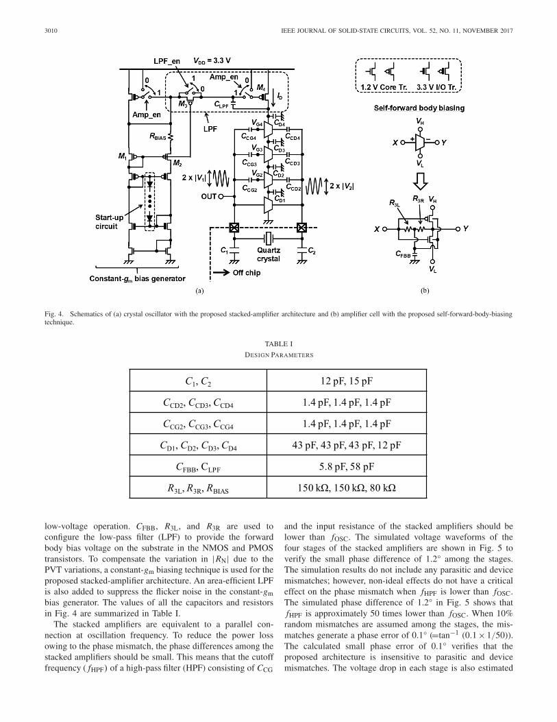
Fig. 4. Schematics of (a) crystal oscillator with the proposed stacked-amplifier architecture and (b) amplifier cell with the proposed self-forward-body-biasingtechnique.
TABLE I
DESIGN PARAMETERS
low-voltage operation. CFBB, R3L, and R3R are used toconfigure the low-pass filter (LPF) to provide the forwardbody bias voltage on the substrate in the NMOS and PMOStransistors. To compensate the variation in |RN| due to thePVT variations, a constant-gm biasing technique is used for theproposed stacked-amplifier architecture. An area-efficient LPFis also added to suppress the flicker noise in the constant-gmbias generator. The values of all the capacitors and resistorsin Fig. 4 are summarized in Table I.
The stacked amplifiers are equivalent to a parallel con-nection at oscillation frequency. To reduce the power lossowing to the phase mismatch, the phase differences among thestacked amplifiers should be small. This means that the cutofffrequency ( fHPF) of a high-pass filter (HPF) consisting of CCG
and the input resistance of the stacked amplifiers should belower than fOSC. The simulated voltage waveforms of thefour stages of the stacked amplifiers are shown in Fig. 5 toverify the small phase difference of 1.2° among the stages.The simulation results do not include any parasitic and devicemismatches; however, non-ideal effects do not have a criticaleffect on the phase mismatch when fHPF is lower than fOSC.The simulated phase difference of 1.2° in Fig. 5 shows thatfHPF is approximately 50 times lower than fOSC. When 10%random mismatches are assumed among the stages, the mis-matches generate a phase error of 0.1° (=tan−1 (0.1 × 1/50)).The calculated small phase error of 0.1° verifies that theproposed architecture is insensitive to parasitic and devicemismatches. The voltage drop in each stage is also estimated

IGUCHI et al.: LOW-POWER CMOS CRYSTAL OSCILLATOR USING STACKED-AMPLIFIER ARCHITECTURE 3011
Fig. 5. Simulated voltage waveforms at OUT, VG2, VG3, and VG4 inthe proposed stacked-amplifier crystal oscillator. The waveform at OUT isdelayed by 83 ps (=1.2°) compared with that at VG2. The phase differencesbetween VG2, VG3, and VG4 are approximately zero owing to the symmetricalconfigurations in the second to fourth stages.
Fig. 6. Simulated relative variation of |RN| with and without the proposedself-forward-body-biasing technique in the worst case (=low temperature andslow corner). VDD(MIN) with the proposed technique is 0.3 V lower than thatwithout the proposed technique.
from the amplitude of the waveforms in Fig. 5. The voltagedrops across the stacked amplifiers at N = 1, 2, 3, and 4 are419, 397, 397, and 396 mV, respectively. It is thus verifiedthat the stacked amplifiers in each stage equally provide thetransconductance.
Fig. 6 shows the simulated relative variation of |RN| withand without the proposed self-forward-body-biasing technique.As discussed above, the proposed stacked-amplifier architec-ture reduces Pdc and PN; however, VDD(MIN) is increased inproportional to N . VDD(MIN) is the fundamental limitationin maximizing the value of N in the proposed stacked-amplifier architecture. To reduce VDD(MIN), specifically in theworst case of a low temperature and slow corner, a newself-forward-body-biasing technique is demonstrated in thispaper. This technique reduces VTH in the NMOS and PMOStransistors by the body effect. Using the self-forward-body-biasing technique, VDD(MIN) in the worst case is reduced by0.3 V compared with that in a stacked-amplifier crystal oscil-lator without the proposed technique. Without the proposed
technique in Fig. 6, the substrates of the NMOS and PMOStransistors are connected to the sources in order to prevent thebody effect. The reduced VDD(MIN) makes it possible to usethe four-stages stacked amplifiers at the supply voltage (VDD)of 3.3 V. Note that the leakage current is not increased bythe self-forward-body-biasing technique because the leakagecurrent is limited by a 3.3-V I/O transistor (M4). VTH in anI/O transistor is approximately two times higher than that ina core transistor. This indicates that the off-resistance in thestacked amplifiers is mainly determined by the I/O transistor.
The proposed self-forward-body-biasing technique reducesthe variation of |RN| in the worst case; however, it doesnot reduce the temperature and supply voltage dependencesof |RN|. To compensate the PVT variations of |RN| in thestacked amplifiers, a constant-gm bias generator is imple-mented. Fig. 7 shows the simulated relative variation of|RN| with and without the constant-gm bias generator. Usingthe constant-gm biasing technique, the supply voltage andtemperature dependences of |RN| are respectively reduced by89% (±24% → ±3%) and 45% (±21% → ±12%) comparedwith those without the constant-gm bias generator.
The constant-gm biasing technique increases PN owing tothe flicker noise in the constant-gm bias generator, althoughthe technique can reduce the PVT variation of |RN|. To reducethe flicker noise from the constant-gm bias generator, an LPFusing an active resistor (M3) and an amplified capacitor (CLPF)based on the Miller effect is developed for the low-noiseoperation of the crystal oscillator. The cutoff frequency of theLPF ( fLPF) is given by
fLPF = 1
2π(1 + ALPF)RON3CLPF(10)
where ALPF is the voltage gain of the common source amplifierof M4 and RON3 is the on-resistance of M3 in the linear region.To suppress the flicker noise around 1 kHz, fLPF shouldbe smaller than 100 Hz. In this paper, RON3 of 27 M� isimplemented with a small area of 1800 μm2 because RBIASis amplified by the size ratio of M1 and M3 as
RON3 ∝ RBIAS × (LM3WM1)/(LM1WM3). (11)
The areas of CLPF and RON3 with the amplified capacitorand active resistor are approximately 10 times and 30 times4
smaller than those with only passive components, respectively.Fig. 8 shows the simulated frequency dependences of I 2
D_n(rms)with and without the area-efficient LPF. The simulation resultverifies that the area-efficient LPF suppresses the flicker noiseof the constant-gm bias generator by 45 dB at 1 kHz.
IV. MEASUREMENT RESULTS AND DISCUSSION
To demonstrate the low-power and low-noise operation ofthe proposed stacked-amplifier architecture, a crystal oscillatoris fabricated in a 65-nm CMOS process. Fig. 9 shows thedie micrograph of the fabricated stacked-amplifier crystaloscillator with a core area of 420 μm × 210 μm. The largearea of CD1, CD2, CD3, and CD4 is a disadvantage of the
4Assumed that the poly resistor has a sheet resistance of 500 � and a widthof 1 μm.

3012 IEEE JOURNAL OF SOLID-STATE CIRCUITS, VOL. 52, NO. 11, NOVEMBER 2017
Fig. 7. Simulated relative variation of |RN| with and without the constant-gm bias generator. (a) and (c) Supply voltage and temperature dependences of |RN|without the bias generator, respectively. (b) and (d) Supply voltage and temperature dependences of |RN| with the bias generator, respectively.
Fig. 8. Simulated frequency dependences of I 2D_n(rms) at |RN| of 50 � with
and without the proposed LPF. To clarify the noise suppression in the LPF,only the noise generated by the constant-gm bias generator is included inthe simulation. The noise current at 1 kHz with the proposed LPF is 45 dBsmaller than that without the LPF.
proposed stacked-amplifier architecture; however, the mini-mum die area of the SoC will be limited by the I/O pinsin many cases. Additionally, the total area of 88 200 μm2 isnot larger than that in conventional works [13], [28]. The areaoverhead should be acceptable in most applications. In thispaper, the characteristic of the quartz crystal is the same asthat in [22] with a load capacitance of 8 pF. To achievean oscillation frequency of 39.25 MHz, C1 of 12 pF, and
Fig. 9. Die micrograph of test chip fabricated in 65-nm CMOS process.
C2 of 15 pF are mounted on an FR4 PCB. The reason whyC1 is smaller than C2 is to increase the oscillation amplitudeat OUT [29].
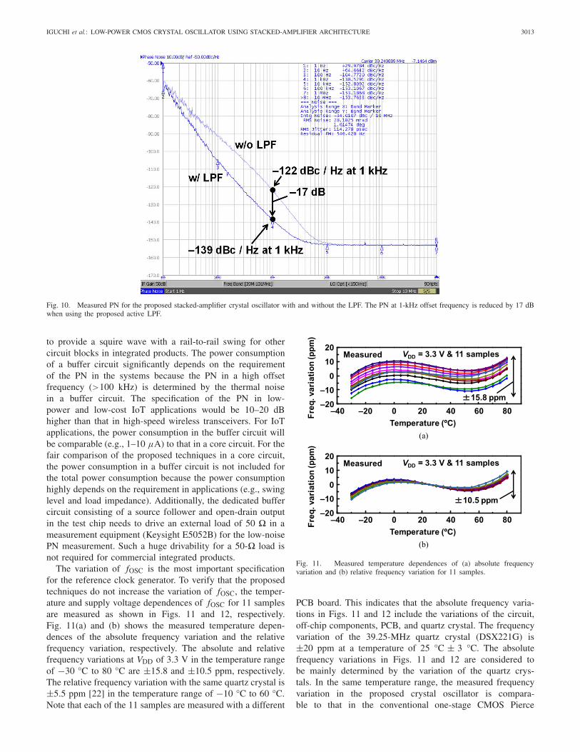
Fig. 10 shows the measured PN with and without an LPF inthe proposed stacked-amplifier crystal oscillator. By enablingthe LPF, PN at 1 kHz offset frequency is reduced from−122 dBc/Hz to −139 dBc/Hz. The 17-dB noise reductionby the area-efficient LPF, consisting of an amplified capacitorand active resistor, clarifies that it successfully suppresses theflicker noise from the constant-gm generator. On the otherhand, PN at offset frequencies higher than 10 kHz is notreduced because the thermal noise in an output buffer isdominant in this frequency range. A buffer circuit is required
IGUCHI et al.: LOW-POWER CMOS CRYSTAL OSCILLATOR USING STACKED-AMPLIFIER ARCHITECTURE 3013
Fig. 10. Measured PN for the proposed stacked-amplifier crystal oscillator with and without the LPF. The PN at 1-kHz offset frequency is reduced by 17 dBwhen using the proposed active LPF.
to provide a squire wave with a rail-to-rail swing for othercircuit blocks in integrated products. The power consumptionof a buffer circuit significantly depends on the requirementof the PN in the systems because the PN in a high offsetfrequency (>100 kHz) is determined by the thermal noisein a buffer circuit. The specification of the PN in low-power and low-cost IoT applications would be 10–20 dBhigher than that in high-speed wireless transceivers. For IoTapplications, the power consumption in the buffer circuit willbe comparable (e.g., 1–10 μA) to that in a core circuit. For thefair comparison of the proposed techniques in a core circuit,the power consumption in a buffer circuit is not included forthe total power consumption because the power consumptionhighly depends on the requirement in applications (e.g., swinglevel and load impedance). Additionally, the dedicated buffercircuit consisting of a source follower and open-drain outputin the test chip needs to drive an external load of 50 � in ameasurement equipment (Keysight E5052B) for the low-noisePN measurement. Such a huge drivability for a 50-� load isnot required for commercial integrated products.
The variation of fOSC is the most important specificationfor the reference clock generator. To verify that the proposedtechniques do not increase the variation of fOSC, the temper-ature and supply voltage dependences of fOSC for 11 samplesare measured as shown in Figs. 11 and 12, respectively.Fig. 11(a) and (b) shows the measured temperature depen-dences of the absolute frequency variation and the relativefrequency variation, respectively. The absolute and relativefrequency variations at VDD of 3.3 V in the temperature rangeof −30 °C to 80 °C are ±15.8 and ±10.5 ppm, respectively.The relative frequency variation with the same quartz crystal is±5.5 ppm [22] in the temperature range of −10 °C to 60 °C.Note that each of the 11 samples are measured with a different
Fig. 11. Measured temperature dependences of (a) absolute frequencyvariation and (b) relative frequency variation for 11 samples.
PCB board. This indicates that the absolute frequency varia-tions in Figs. 11 and 12 include the variations of the circuit,off-chip components, PCB, and quartz crystal. The frequencyvariation of the 39.25-MHz quartz crystal (DSX221G) is±20 ppm at a temperature of 25 °C ± 3 °C. The absolutefrequency variations in Figs. 11 and 12 are considered tobe mainly determined by the variation of the quartz crys-tals. In the same temperature range, the measured frequencyvariation in the proposed crystal oscillator is compara-ble to that in the conventional one-stage CMOS Pierce

3014 IEEE JOURNAL OF SOLID-STATE CIRCUITS, VOL. 52, NO. 11, NOVEMBER 2017
Fig. 12. Measured supply voltage dependences of (a) absolute frequencyvariation and (b) relative frequency variation for 11 samples.
crystal oscillator. This verifies that the proposed techniquesdo not increase the frequency variation.
In the same way, the measured supply voltage dependencesof the absolute frequency variation and the relative frequencyvariation are shown in Figs. 12(a) and (b), respectively. Theabsolute and relative frequency variations at a temperatureof 25 °C at VDD of 3.3 V ±10% are ±7.2 and ±0.12 ppm,respectively. The supply voltage dependence of the frequencyvariation in the proposed crystal oscillator is also well matchedto the relative frequency variation of ±0.6 ppm [22] in theconventional oscillator with VDD of 1.5 V ± 20%. Thesemeasured results in Figs. 11 and 12 clearly show that theproposed crystal oscillator can be used as a reference clockgenerator for low-energy wireless communications.
Fig. 13(a) and (b) shows the measured time dependenceof the frequency variation as a linear–linear plot and a log–linear plot, respectively. To evaluate the aging effect in theproposed crystal oscillator, fOSC is measured for 32 days at atemperature of 25 °C and VDD of 3.3 V. The measured long-term frequency variation for 32 days is −0.57 ppm and thepredicted frequency variation in the first year (=365 days) is−0.98 ppm. The long-term frequency variation is derived byextrapolation of the logarithmic function [30] using the datafrom 10 to 32 days. The data until 10 days are excludedfrom the extrapolation because fOSC is unstable in the firstseveral days. The measured long-term frequency variation of−0.98 ppm/year is comparable to that of conventional crystaloscillators (e.g., 2.5 ppm/year [31]).
The Allan deviation is also used to evaluate the time-domain frequency stability of oscillators. To evaluate thefrequency stability of the proposed crystal oscillator, the Allandeviation (σy) is calculated from the measured PN in the offsetfrequency of 1 Hz to 10 MHz using [32]
σy = 2
πτ fOSC
√∫ fH
010PN/10 × sin4(πτ f )d f (12)
Fig. 13. Measured time dependences of the frequency variation:(a) linear–linear plot and (b) log–linear plot. The predicted frequency variationin the first year (=365 days) is −0.98 ppm.
Fig. 14. Measured start-up waveforms.
where fH is the upper cutoff frequency of the measuringsystem and τ is the observation time. The calculated Allandeviations at τ = 0.1 and 1 s are 1.1 × 10⁻⁹ and 1.7 × 10⁻¹⁰,respectively.
The measured start-up waveforms of the proposed crystaloscillator are shown in Fig. 14. To prevent a long start-up time (tSTART) owing to the LPF used for flicker noisesuppression, the LPF is disabled during the startup. WhenLPF_en is enabled after 4 ms from Amp_en, the measuredstart-up time is 3.9 ms. The start-up time and energy are alsoimportant specifications in IoT applications. Several quick-startup and energy-reduction techniques have been demon-strated recently [22], [33], [34]. These techniques can beapplicable to the proposed architecture because the stacked-amplifier architecture is equivalent to the Pierce crystal oscil-lator. Using these techniques, the start-up time can easily bereduced to less than 1 ms. The proposed architecture is ableto support the quick-startup and energy-reduction techniquesin low-energy IoT applications.

IGUCHI et al.: LOW-POWER CMOS CRYSTAL OSCILLATOR USING STACKED-AMPLIFIER ARCHITECTURE 3015
TABLE II
COMPARISON WITH PREVIOUS WORKS
A summary of the performances of the proposed crys-tal oscillator [9] and a comparison with those in previousworks [13], [14], [17], [22], [28], [33] are shown in Table IIin chronological order. The proposed stacked-amplifier crys-tal oscillator demonstrates the smallest ever reported FoMof −248 dBc/Hz for a crystal oscillator. The values of FoMin [9] and [22] are 30 dB larger than that in Table II, becausethe power consumption was normalized by the unit of watt inthe previous publications. However, the power consumptionis normalized by the unit of milliwatt in many studies onhigh-frequency oscillators [8]. To prevent confusion due tothe different definitions among studies, all values of FoMin Table II are calculated with the unit of milliwatt. The currentconsumption of 5.8 μA is achieved by the proposed powerreduction technique of the stacked-amplifier architecture. Therelative frequency errors among the 11 samples at temperaturesof −30 °C to 80 °C and for ±10% supply voltage variation are±10.5 ppm and ±0.12 ppm (=±0.18 ppm/V), respectively.
V. CONCLUSION
A low-power 39.25-MHz crystal oscillator with astacked-amplifier architecture was presented. The proposedstacked-amplifier architecture reduces the power consumptionby 91% in the case of four stages of stacked amplifiers.New theoretical analyses of the power consumption and PNin a proposed stacked-amplifier crystal oscillator clarify thereason why the proposed oscillator achieves the smallest everreported FoM of −248 dBc/Hz with a power consumptionof 19 μW and PN of −139 dBc/Hz at 1-kHz offset frequency.A new self-forward-body-biasing technique and flicker noisesuppression technique were also presented, which reduce theminimum operational supply voltage (VDD(MIN)) and the PN,respectively. Using the proposed self-forward-body-biasingtechnique, VDD(MIN) in the worst case (−30 °C and a slowcorner) is reduced by 0.3 V, thereby achieving reliable oper-ation even with PVT variations. The measurement results
Fig. 15. Equivalent circuit of the N -stages stacked amplifiers.
for 11 samples verify the reliable and accurate frequencygeneration of the proposed crystal oscillator with relativefrequency errors of ±10.5 and ±0.12 ppm at temperature of−30 °C to 80 °C and for ±10% supply voltage variation,respectively.
APPENDIX
DERIVATION OF (8)
The detailed derivation of (8) is given in this Appendix. Theequivalent circuit of the N-stages stacked amplifiers is shownin Fig. 15. The equivalent resistances of the NMOS and PMOStransistors are denoted as REQ_N and REQ_P, respectively. Thesquares of the equivalent flicker noise voltage (V 2
1/f_n(rms)) ofthe NMOS and PMOS transistors are denoted as V 2
1/f_n(rms)_Nand V 2
1/f_n(rms)_P, respectively. Using the relationship gmN =gmP = gm(TOTAL)/(2 × N) and Thevenin’s theorem, the totalequivalent resistance (REQ_TOTAL) and the total square of theequivalent flicker noise voltage (V 2
1/f_n(rms)_TOTAL) are givenas
REQ_TOTAL = N ×(
1
gmN+ 1
gmP
)= 4N2
gm(TOTAL)(A1)

3016 IEEE JOURNAL OF SOLID-STATE CIRCUITS, VOL. 52, NO. 11, NOVEMBER 2017
and
V 21/f_n(rms)_TOTAL = N × (V 2
1/f_n(rms)_N + V 21/f_n(rms)_P)
= N ×(
KN
ωLNWN+ KP
ωLPWP
). (A2)
Using (A1) and (A2), I 2D_n(rms) for the N-stages stacked
amplifiers is derived as
I 2D_n(rms) =
V 21/f_n(rms)_TOTAL
R2EQ_TOTAL
= (nKN + KP)g2m(TOTAL)
16nωN3 LNWN(A3)
assuming with the relationships LN = LP and n ×WN = WP.
ACKNOWLEDGMENT
The authors would like to thank Y. Yoshihara, Y. Niki, andR. Fujimoto of Toshiba Corporation for technical discussions,and R. Shidachi and S. Lee of The University of Tokyo forsupport in the measurements.
REFERENCES
[1] A. M. Nicolson, “Generating and transmitting electric currents,”U.S. Patent 2,212,845 A, Aug. 27, 1940.
[2] W. G. Cady, “Method of maintaining electric currents of constantfrequency,” U.S. Patent 1,472,583 A, Oct. 30, 1923.
[3] R. J. Thompson, Jr., Crystal Clear: The Struggle for Reliable Communi-cations Technology in World War II, 1st ed. Hoboken, NJ, USA: Wiley,2011.
[4] E. Vittoz and J. Fellrath, “CMOS analog integrated circuits based onweak inversion operations,” IEEE J. Solid-State Circuits, vol. SSC-12,no. 3, pp. 224–231, Jun. 1977.
[5] E. A. Vittoz, M. G. R. Degrauwe, and S. Bitz, “High-performance crystaloscillator circuits: Theory and application,” IEEE J. Solid-State Circuits,vol. SSC-23, no. 3, pp. 774–783, Jun. 1988.
[6] L. Atzori, A. Lera, and G. Morabito, “The Internet of Things: A survey,”Comput. Netw., vol. 54, no. 15, pp. 2787–2805, Oct. 2010.
[7] Bluetooth Special Interest Group (SIG). (2014). Specification of theBluetooth System, Core Package Version 4.2, Bluetooth Specifications,Bluetooth Special Interest Group (SIG). [Online]. Available: https://www.bluetooth.org/DocMan/handlers/DownloadDoc.ashx?doc_id=286439
[8] W. Deng, K. Okada, and A. Matsuzawa, “Class-C VCO with amplitudefeedback loop for robust start-up and enhanced oscillation swing,” IEEEJ. Solid-State Circuits, vol. 48, no. 2, pp. 429–440, Feb. 2013.
[9] S. Iguchi, T. Sakurai, and M. Takamiya, “A 39.25 MHz 278 dB-FOM19 μW LDO-free stacked-amplifier crystal oscillator (SAXO) operatingat I/O voltage,” in IEEE Int. Solid-State Circuits Conf. (ISSCC) Dig.Tech. Papers, Feb. 2016, pp. 100–101.
[10] J. T. Santos and R. G. Meyer, “A one-pin crystal oscillator for VLSIcircuits,” IEEE J. Solid-State Circuits, vol. SSC-19, no. 2, pp. 228–236,Apr. 1984.
[11] D. Aebischer, H. J. Oguey, and V. R. V. Kaenel, “A 2.1-MHz crystaloscillator time base with a current consumption under 500 nA,” IEEEJ. Solid-State Circuits, vol. 32, no. 7, pp. 999–1005, Jul. 1997.
[12] D. Ruffieux, “A high-stability, ultra-low-power quartz differential oscil-lator circuit for demanding radio applications,” in Proc. 28th Eur. Solid-State Circuits Conf., Sep. 2002, pp. 85–88.
[13] Y. Chang, J. Leete, Z. Zhou, M. Vadipour, Y.-T. Chang, and H. Darabi,“A differential digitally controlled crystal oscillator with a 14-bit tun-ing resolution and sine wave outputs for cellular applications,” IEEEJ. Solid-State Circuits, vol. 47, no. 2, pp. 421–434, Feb. 2012.
[14] M. M. Ghahramani, Y. Rajavi, A. Khalili, A. Kavousian, B. Kim, andM. P. Flynn, “A 192 MHz differential XO based frequency quadruplerwith sub-picosecond jitter in 28 nm CMOS,” in IEEE Radio Freq. Integr.Circuits Conf. Dig. Tech. Papers, May 2015, pp. 59–62.
[15] U. Karthaus, “A differential two-pin crystal oscillator–concept, analysis,and implementation,” IEEE Trans. Circuits Syst. II, Exp. Briefs, vol. 53,no. 10, pp. 1073–1077, Oct. 2006.
[16] D. Ruffieux et al., “A 3.2×1.5×0.8 mm3 240 nA 1.25-to-5.5 V32 kHz-DTCXO RTC module with an overall accuracy of ±1 ppm andan all-digital 0.1 ppm compensation-resolution scheme at 1 Hz,” in IEEEInt. Solid-State Circuits Conf. (ISSCC) Dig. Tech. Papers, Feb. 2016,pp. 208–209.
[17] S. Iguchi, A. Saito, Y. Zheng, K. Watanabe, T. Sakurai, andM. Takamiya, “93% power reduction by automatic self power gating(ASPG) and multistage inverter for negative resistance (MINR) in 0.7 V,9.2 μW, 39 MHz crystal oscillator,” in IEEE Symp. VLSI Circuits Dig.Tech. Papers, Jun. 2013, pp. C142–C143.
[18] A. Shrivastava, D. A. Kamakshi, and B. H. Calhoun, “A 1.5 nW,32.768 kHz XTAL oscillator operational from a 0.3 V supply,” IEEEJ. Solid-State Circuits, vol. 51, no. 3, pp. 686–696, Mar. 2016.
[19] K.-J. Hsiao, “A 1.89 nW/0.15 V self-charged XO for real-time clockgeneration,” in IEEE Int. Solid-State Circuits Conf. (ISSCC) Dig. Tech.Papers, Feb. 2014, pp. 298–299.
[20] D. Yoon, T. Jang, D. Sylvester, and D. Blaauw, “A 5.58 nW crystaloscillator using pulsed driver for real-time clocks,” IEEE J. Solid-StateCircuits, vol. 51, no. 2, pp. 509–522, Feb. 2016.
[21] A. Rusznyak, “Start-up time of CMOS oscillators,” IEEE Trans. CircuitsSyst., vol. CAS-34, no. 3, pp. 259–268, Mar. 1987.
[22] S. Iguchi, H. Fuketa, T. Sakurai, and M. Takamiya, “Variation-tolerantquick-start-up CMOS crystal oscillator with chirp injection and neg-ative resistance booster,” IEEE J. Solid-State Circuits, vol. 51, no. 2,pp. 496–508, Feb. 2016.
[23] T. C. Carusone, D. Johns, and K. Martin, Analog Integrated CircuitDesign, 2nd ed. Hoboken, NJ, USA: Wiley, 2011.
[24] A. Hajimiri and T. H. Lee, “A general theory of phase noise in electricaloscillators,” IEEE J. Solid-State Circuits, vol. 33, no. 2, pp. 179–194,Feb. 1998.
[25] T. H. Lee and A. Hajimiri, “Oscillator phase noise: A tutorial,” IEEEJ. Solid-State Circuits, vol. 35, no. 3, pp. 326–336, Mar. 2000.
[26] E. Vittoz, Low-Power Crystal and MEMS Oscillators, 1st ed. Berlin,Germany: Springer, 2010.
[27] Y. Tsividis and C. McAndrew, Operation and Modeling of the MOSTransistor, 3rd ed. Oxford, U.K.: Oxford Univ. Press, 2011.
[28] J. Lin, “A low-phase-noise 0.004-ppm/step DCXO with guaranteedmonotonicity in the 90-nm CMOS process,” IEEE J. Solid-State Circuits,vol. 40, no. 12, pp. 2726–2734, Dec. 2005.
[29] S. G. de A. Garcin, “Crystal oscillator troubleshooting guide,” FreescaleSemiconductor, Austin, TX, USA, Appl. Note AN3208, 2006. [Online].Available: http://www.nxp.com/assets/documents/data/en/application-notes/AN3208.pdf
[30] R. L. Filler and J. R. Vig, “Long-term aging of oscillators,”IEEE Trans. Ultrason., Ferroelect., Freq. Control, vol. 40, no. 4,pp. 387–394, Jul. 1993.
[31] R. A. Bianchi, J. M. Karam, and B. Courtois, “Analog ALC crystal oscil-lators for high-temperature applications,” IEEE J. Solid-State Circuits,vol. 35, no. 1, pp. 2–14, Jan. 2000.
[32] R. M. Cerda, Understanding Quartz Crystals and Oscillators, 1st ed.Norwood, MA, USA: Artech House, 2014.
[33] D. Griffith, J. Murdock, and P. T. Røine, “A 24 MHz crystal oscillatorwith robust fast start-up using dithered injection,” in IEEE Int. Solid-State Circuits Conf. (ISSCC) Dig. Tech. Papers, Jan. 2016, pp. 104–105.
[34] M. Ding et al., “A 95 μW 24 MHz digitally controlled crystal oscillatorfor IoT applications with 36 nJ start-up energy and >13× start-up timereduction using a fully-autonomous dynamically-adjusted load,” in IEEEInt. Solid-State Circuits Conf. (ISSCC) Dig. Tech. Papers, Feb. 2017,pp. 90–91.
Shunta Iguchi (S’12–M’16) received the B.S.degree in electronic engineering from The Uni-versity of Electro-Communications, Tokyo, Japan,in 2011, and the M.S. and Ph.D. degrees in electri-cal engineering and information systems from TheUniversity of Tokyo, Tokyo, in 2013 and 2016,respectively.
He joined Analog Devices, Tokyo, Japan, in 2011,Toshiba, Kanagawa, Japan, in 2013, and TSMC,Hsinchu, Taiwan, in 2014, as an Intern. He was aProject Researcher with The University of Tokyo
in 2016. In 2016, he joined Qualcomm, San Diego, CA, USA, where heis involved in the circuit design of ultra-low-noise oscillators for smartphonechipsets. His current research interests include the design of low-power andlow-noise oscillators, RF transceiver circuits, and wireless power transmissioncircuits.
Dr. Iguchi was a recipient of the Outstanding Award in NE AnalogInnovation Award 2016 and the Best Paper Award at the 2013 IEEE WirelessPower Transfer Conference.

IGUCHI et al.: LOW-POWER CMOS CRYSTAL OSCILLATOR USING STACKED-AMPLIFIER ARCHITECTURE 3017
Takayasu Sakurai (S’77–M’78–SM’01–F’03)received the Ph.D. degree in electrical engineeringfrom The University of Tokyo, Tokyo, Japan,in 1981.
In 1981, he joined Toshiba Corporation, Kawasaki,Japan, where he was involved in the design ofCMOS DRAM, SRAM, RISC processors, DSPs,and system-on-chip Solutions. He was involvedextensively on interconnect delay and capacitancemodeling known as Sakurai model and alphapower-law MOS model. From 1988 to 1990,
he was a Visiting Researcher at the University of California, Berkeley,CA, USA, where he conducted research in the field of very large scaleintegration (VLSI) CAD. Since 1996, he has been a Professor with TheUniversity of Tokyo, where he was involved in low-power high-speedVLSI, memory design, interconnects, ubiquitous electronics, organic IC’sand large-area electronics. He has authored or co-authored more than600 technical publications including 100 invited presentations and severalbooks and holds more than 200 patents.
Dr. Sakurai is an IEICE Fellow. He served as an Executive CommitteeMember of ISLPED and a Program Committee Member of ISSCC,CICC, A-SSCC, DAC, ESSCIRC, ICCAD, ISLPED, and other internationalconferences. He was a recipient of the 2010 IEEE Donald O. Pederson Awardin Solid-State Circuits, the 2009 and 2010 IEEE Paul Rappaport Award,the 2010 IEICE Electronics Society Award, the 2009 IEICE AchievementAward, the 2005 IEEE ICICDT Award, the 2004 IEEE Takuo Sugano Award,and the 2005 P&I Patent of the Year Award and four product awards. He wasthe Executive Committee Chair of the VLSI Symposia and the SteeringCommittee Chair of the IEEE A-SSCC. He served as the ConferenceChair of the Symposium on the VLSI Circuits and ICICDT, the Vice Chairof ASPDAC, and the TPC Chair of the A-SSCC and VLSI symposium.He delivered keynote speech at more than 50 conferences including ISSCC,ESSCIRC, and ISLPED. He was an elected AdCom Member of the IEEESolid-State Circuits Society and the IEEE CAS and SSCS DistinguishedLecturer. He is also a Domain Research Supervisor for nano-electronics areawith Japan Science and Technology Agency.
Makoto Takamiya (S’98–M’00–SM’14) receivedthe B.S., M.S., and Ph.D. degrees in electronicengineering from The University of Tokyo, Tokyo,Japan, in 1995, 1997, and 2000, respectively.
In 2000, he joined NEC Corporation, Sagamihara,Japan, where he was involved in the circuit designof high-speed digital LSIs. In 2005, he joined TheUniversity of Tokyo, where he is an Associate Pro-fessor with the VLSI Design and Education Center.From 2013 to 2014, he was a Visiting Scholar at theUniversity of California, Berkeley, CA, USA. His
current research interests include the integrated power management circuitsfor the ultralow power Internet of Things applications and the digital gatedriver circuits for IGBT.
Dr. Takamiya is a member of the technical program committee of the IEEEInternational Solid-State Circuits Conference and the IEEE Symposium onVLSI Circuits. He received the 2009 and 2010 IEEE Paul Rappaport Awardsand the Best Paper Award in 2013 IEEE Wireless Power Transfer Conference.