3 Failure Mechanism of Semiconductor Devices · PDF file3 Failure Mechanism of Semiconductor...
60
3 Failure Mechanism of Semiconductor Devices
Transcript of 3 Failure Mechanism of Semiconductor Devices · PDF file3 Failure Mechanism of Semiconductor...
3 Failure Mechanism of SemiconductorDevices
Contents
3.1 Reliability Factor and Failure Mechanism of
Semiconductor Devices 3- 1
3.1.1 Reliability factors 3- 1
3.1.2 Failure factors and mechanisms of
semiconductor devices 3- 4
3.2 Failure Mechanisms of Semiconductor Devices 3- 6
3.2.1 Time dependent dielectric breakdown (TDDB) 3- 6
3.2.2 Slow trap (NBTI) 3- 8
3.2.3 Hot carrier (AHC) 3-10
3.2.4 Soft error 3-12
3.2.5 Reliability problem of nonvolatile memory 3-14
3.2.6 Electromigration (EM) 3-16
3.2.7 Stress migration (SM) 3-20
3.2.8 Reliability of Cu wire 3-23
3.2.9 Al corrosion 3-25
3.2.10 Passivation crack 3-32
3.2.11 Growth of Au/Al compound 3-35
3.2.12 Secondary breakdown 3-36
3.2.13 Thermal fatigue 3-37
3.2.14 Ion migration 3-38
3.2.15 Sn whisker 3-39
3.2.16 Problems in surface mounting
(package cracking) 3-40
3.2.17 Electrostatic discharge (ESD) 3-44
3.2.18 Latch-up 3-53
i
Failure Mechanism of Semiconductor Devices
T04007BE-3 2009.4 3-1
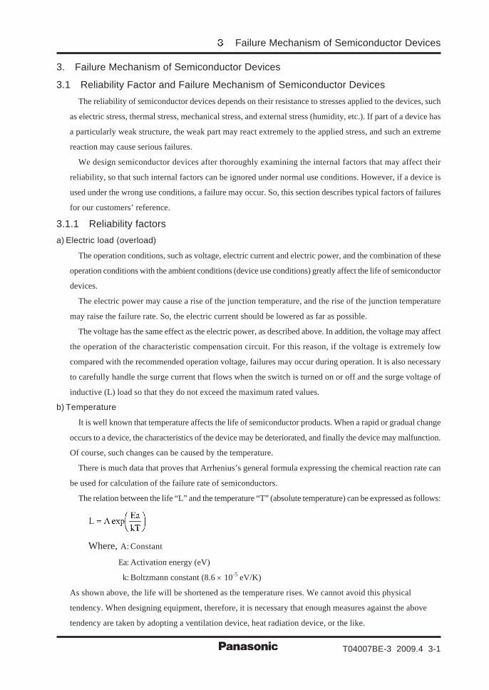
3. Failure Mechanism of Semiconductor Devices
3.1 Reliability Factor and Failure Mechanism of Semiconductor DevicesThe reliability of semiconductor devices depends on their resistance to stresses applied to the devices, such
as electric stress, thermal stress, mechanical stress, and external stress (humidity, etc.). If part of a device has
a particularly weak structure, the weak part may react extremely to the applied stress, and such an extreme
reaction may cause serious failures.
We design semiconductor devices after thoroughly examining the internal factors that may affect their
reliability, so that such internal factors can be ignored under normal use conditions. However, if a device is
used under the wrong use conditions, a failure may occur. So, this section describes typical factors of failures
for our customers’ reference.
3.1.1 Reliability factorsa) Electric load (overload)
The operation conditions, such as voltage, electric current and electric power, and the combination of these
operation conditions with the ambient conditions (device use conditions) greatly affect the life of semiconductor
devices.
The electric power may cause a rise of the junction temperature, and the rise of the junction temperature
may raise the failure rate. So, the electric current should be lowered as far as possible.
The voltage has the same effect as the electric power, as described above. In addition, the voltage may affect
the operation of the characteristic compensation circuit. For this reason, if the voltage is extremely low
compared with the recommended operation voltage, failures may occur during operation. It is also necessary
to carefully handle the surge current that flows when the switch is turned on or off and the surge voltage of
inductive (L) load so that they do not exceed the maximum rated values.
b) Temperature
It is well known that temperature affects the life of semiconductor products. When a rapid or gradual change
occurs to a device, the characteristics of the device may be deteriorated, and finally the device may malfunction.
Of course, such changes can be caused by the temperature.
There is much data that proves that Arrhenius’s general formula expressing the chemical reaction rate can
be used for calculation of the failure rate of semiconductors.
The relation between the life “L” and the temperature “T” (absolute temperature) can be expressed as follows:
Where, A: Constant
Ea: Activation energy (eV)
k: Boltzmann constant (8.6 × 10⁻⁵ eV/K)
As shown above, the life will be shortened as the temperature rises. We cannot avoid this physical
tendency. When designing equipment, therefore, it is necessary that enough measures against the above
tendency are taken by adopting a ventilation device, heat radiation device, or the like.
3 Failure Mechanism of Semiconductor Devices
T04007BE-3 2009.4 3-2
The term “Ea” in Arrhenius’s formula is referred to as the activation energy and represents the amount of
energy needed for activation of the reaction that can cause a failure. The “Ea” value depends on the failure
mechanism as shown below:
Defect of oxide film: 0.3 eV to 1.1 eV
Drift of ionicity (Na ions in oxide film): 0.7 eV to 1.8 eV
Slow trap: 0.8 eV to 1.2 eV
Electromigration disconnection:
for Al wire 0.5 eV to 0.7 eV
for Cu wire 0.8 eV to 1.0 eV
Metal (Al) corrosion: 0.7 eV to 0.9 eV
Growth of compound between metals (Au-Al): 1.0 eV to 1.3 eV
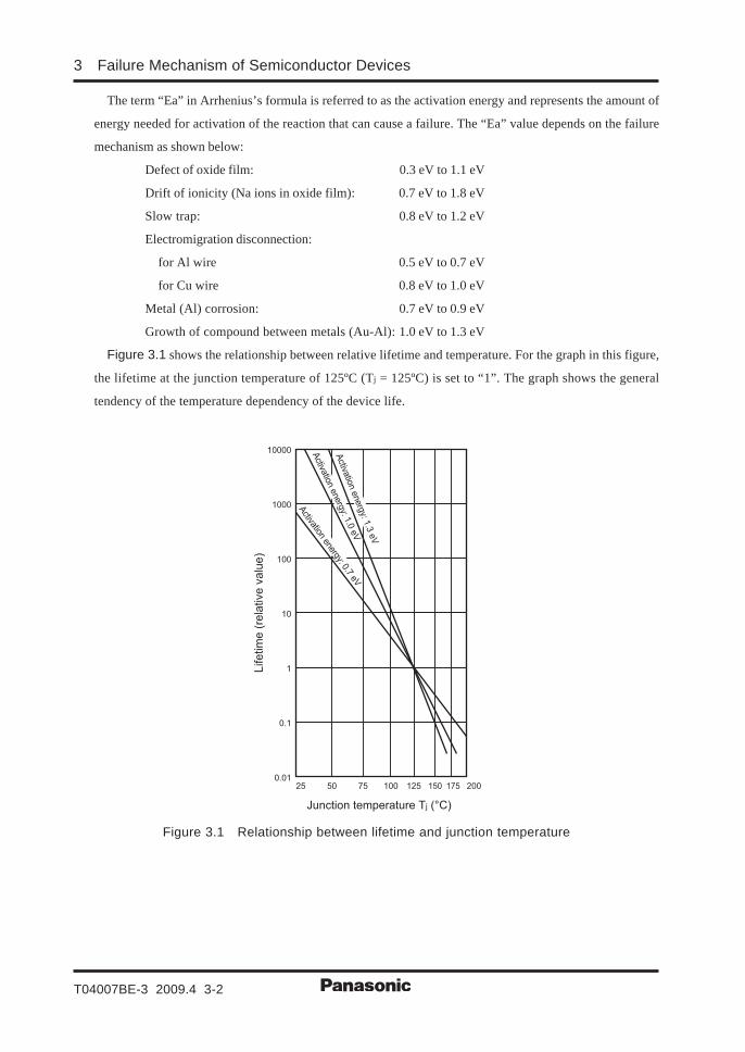
Figure 3.1 shows the relationship between relative lifetime and temperature. For the graph in this figure,
the lifetime at the junction temperature of 125ºC (Tj = 125ºC) is set to “1”. The graph shows the general
tendency of the temperature dependency of the device life.
1000
10000
100
10
1
0.1
0.0175 2005025 125100 150 175
Activation energy: 0.7 eV
Activation energy: 1.0 eV
Activa
tion e
nerg
y: 1.3
eV
Lifetim
e (
rela
tive v
alu
e)
Junction temperature Tj (°C)
Figure 3.1 Relationship between lifetime and junction temperature
Failure Mechanism of Semiconductor Devices
T04007BE-3 2009.4 3-3
c) Humidity
The surface of each IC chip is covered with surface protective film. For this reason, IC chips are not easily
affected by humidity.
Resin molded devices, however, are water permeable. So, water can gradually permeate this type of device.
So, if a resin molded device is operated for a long time at a high temperature and high humidity, the device may
malfunction. If it is expected that the device is operated under severe humidity conditions, it should be
operated particularly carefully.
d) Mechanical stress
If the device is strongly vibrated during transportation, or if an extremely strong force is applied to a device
during installation, the device may be directly, mechanically damaged. In addition, moisture or a contaminant
may enter the device through the damaged area, and may cause deterioration of the device.
e) Static electricity
Equipment incorporating devices is often charged with static electricity. In some cases, an electrostatic charge
damages the equipment. Recently, plastic is generally used for the casing and the structure of equipment. For
this reason, when our customers use our semiconductor devices for their products, we ask them to consider
how to prevent electrostatic charge.
In addition, human bodies can be also charged with static electricity. So, when handling semiconductor
devices, it is necessary to take static charge preventive measures. You may think that electrostatic destruction
is a problem peculiar to MOS devices. However, this problem also occurs on the other types of devices as the
products are more miniaturized and higher frequencies are adopted. So, any type of semiconductor device
should be handled carefully.
f) Effect of repeated stress
When a stress is repeatedly applied, the applied stress may be stronger than steady stress. For example,
a high-low temperature cycle and intermittent internal heat generation cycle can apply stresses repeatedly.
The effects of these cycles, such as rearrangement of the material structure and fatigue deterioration of
resistance to distortion, are examined and utilized for evaluation of failures.
3 Failure Mechanism of Semiconductor Devices
T04007BE-3 2009.4 3-4
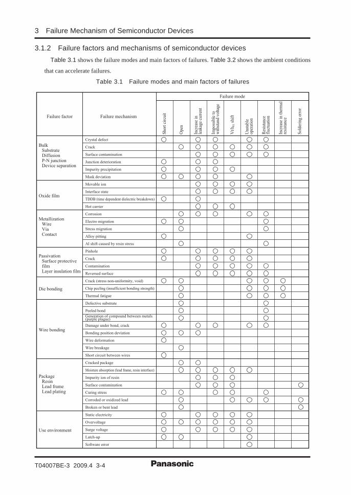
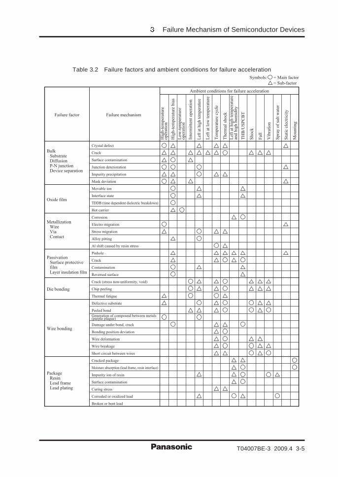
3.1.2 Failure factors and mechanisms of semiconductor devicesTable 3.1 shows the failure modes and main factors of failures. Table 3.2 shows the ambient conditions
that can accelerate failures.
Table 3.1 Failure modes and main factors of failures
Failure factor Failure mechanism
Failure mode
Bulk Substrate Diffusion P-N junction Device separation
Metallization Wire Via Contact
Passivation Surface protective film Layer insulation film
Package Resin Lead frame Lead plating
Oxide film
Die bonding
Use environment
Wire bonding
Crystal defect
Crack
Surface contamination
Junction deterioration
Impurity precipitation
Mask deviation
Movable ion
Interface state
TDDB (time dependent dielectric breakdown)
Hot carrier
Corrosion
Electro migration
Stress migration
Alloy pitting
Al shift caused by resin stress
Pinhole
Crack
Contamination
Reversed surface
Crack (stress non-uniformity, void)
Chip peeling (insufficient bonding strength)
Thermal fatigue
Defective substrate
Peeled bond
Generation of compound between metals (purple plague)
Damage under bond, crack
Bonding position deviation
Wire deformation
Wire breakage
Short circuit between wires
Cracked package
Moisture absorption (lead frame, resin interface)
Impurity ion of resin
Surface contamination
Curing stress
Corroded or oxidized lead
Broken or bent lead
Static electricity
Overvoltage
Surge voltage
Latch-up
Software error
Sho
rt c
ircu
it
Ope
n
Incr
ease
in
leak
age
curr
ent
Impo
ssib
le t
o w
iths
tand
vol
tage
Vt/
h FE s
hift
Uns
tabl
e op
erat
ion
Res
ista
nce
fluc
tuat
ion
Incr
ease
in
ther
mal
re
sist
ance
Sol
deri
ng e
rror
Failure Mechanism of Semiconductor Devices
T04007BE-3 2009.4 3-5
Table 3.2 Failure factors and ambient conditions for failure acceleration
Failure factor
Crystal defect
Crack
Surface contamination
Junction deterioration
Impurity precipitation
Mask deviation
Movable ion
Interface state
TDDB (time dependent dielectric breakdown)
Hot carrier
Corrosion
Electro migration
Stress migration
Alloy pitting
Al shift caused by resin stress
Pinhole
Crack
Contamination
Reversed surface
Crack (stress non-uniformity, void)
Chip peeling
Thermal fatigue
Defective substrate
Peeled bond
Generation of compound between metals (purple plague)
Damage under bond, crack
Bonding position deviation
Wire deformation
Wire breakage
Short circuit between wires
Cracked package
Moisture absorption (lead frame, resin interface)
Impurity ion of resin
Surface contamination
Curing stress
Corroded or oxidized lead
Broken or bent lead
Failure mechanism
Ambient conditions for failure acceleration
Bulk Substrate Diffusion P-N junction Device separation
Metallization Wire Via Contact
Passivation Surface protective film Layer insulation film
Package Resin Lead frame Lead plating
Oxide film
Die bonding
Wire bonding
Symbols: = Main factor
= Sub-factor
Hig
h-t
emp
erat
ure
o
per
atio
n
Hig
h-t
emp
erat
ure
bia
s
Lo
w-t
emp
erat
ure
o
per
atio
n
Inte
rmit
ten
t o
per
atio
n
Lef
t at
hig
h t
emp
erat
ure
Lef
t at
lo
w t
emp
erat
ure
Tem
per
atu
re c
ycl
e
Th
erm
al s
ho
ck
Lef
t at
hig
h t
emp
erat
ure
an
d h
igh
hu
mid
ity
TH
B/U
SP
CB
T
Sh
ock
Fal
l
Vib
rati
on
Sp
ray
of
salt
wat
er
Sta
tic
elec
tric
ity
Mo
un
tin
g
3 Failure Mechanism of Semiconductor Devices
T04007BE-3 2009.4 3-6
3.2 Failure Mechanisms of Semiconductor Devices
3.2.1 Time dependent dielectric breakdown (TDDB)As integrated circuits are miniaturized, the gate oxide films are becoming extremely thin, and in these oxide
films, the electric field strength is getting ever stronger. Oxide film breakage is caused by either an initial defect
or deterioration of the oxide film. The former breakage will result in an early failure, and the latter breakage
will result in a long-term reliability failure. It is generally said that the true withstand voltage against dielectric
breakdown is 10 MV/cm for oxide films. For this reason, when the electric field applied to an oxide film
exceeds this dielectric breakdown withstand voltage, the oxide film may be broken. However, even if an oxide
film is put to practical use in an electric field of 2 MV/cm to 5 MV/cm (low enough compared with the dielectric
breakdown withstand voltage of oxide films), continuous application of such a low electric field for a long
time may also cause breakage as time elapses. This type of breakage is referred to as a time dependent
dielectric breakdown (TDDB).
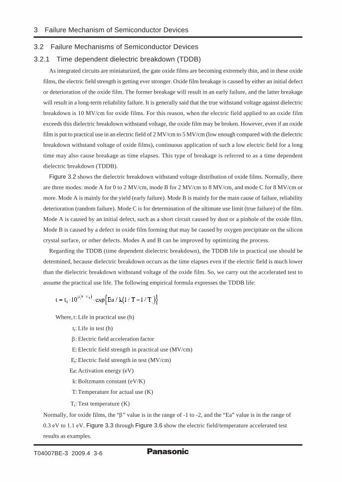
Figure 3.2 shows the dielectric breakdown withstand voltage distribution of oxide films. Normally, there
are three modes: mode A for 0 to 2 MV/cm, mode B for 2 MV/cm to 8 MV/cm, and mode C for 8 MV/cm or
more. Mode A is mainly for the yield (early failure). Mode B is mainly for the main cause of failure, reliability
deterioration (random failure). Mode C is for determination of the ultimate use limit (true failure) of the film.
Mode A is caused by an initial defect, such as a short circuit caused by dust or a pinhole of the oxide film.
Mode B is caused by a defect in oxide film forming that may be caused by oxygen precipitate on the silicon
crystal surface, or other defects. Modes A and B can be improved by optimizing the process.
Regarding the TDDB (time dependent dielectric breakdown), the TDDB life in practical use should be
determined, because dielectric breakdown occurs as the time elapses even if the electric field is much lower
than the dielectric breakdown withstand voltage of the oxide film. So, we carry out the accelerated test to
assume the practical use life. The following empirical formula expresses the TDDB life:
Where, t: Life in practical use (h)
tt: Life in test (h)
β: Electric field acceleration factor
E: Electric field strength in practical use (MV/cm)
Et: Electric field strength in test (MV/cm)
Ea: Activation energy (eV)
k: Boltzmann constant (eV/K)
T: Temperature for actual use (K)
Tt: Test temperature (K)
Normally, for oxide films, the “β” value is in the range of -1 to -2, and the “Ea” value is in the range of
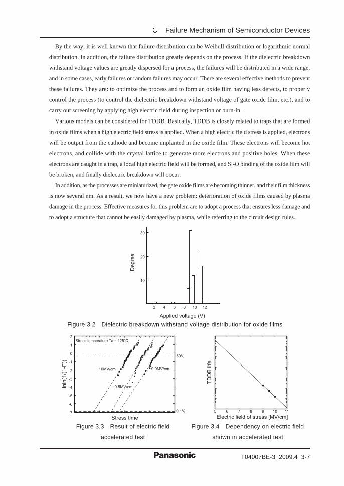
0.3 eV to 1.1 eV. Figure 3.3 through Figure 3.6 show the electric field/temperature accelerated test
results as examples.
Failure Mechanism of Semiconductor Devices
T04007BE-3 2009.4 3-7
By the way, it is well known that failure distribution can be Weibull distribution or logarithmic normal
distribution. In addition, the failure distribution greatly depends on the process. If the dielectric breakdown
withstand voltage values are greatly dispersed for a process, the failures will be distributed in a wide range,
and in some cases, early failures or random failures may occur. There are several effective methods to prevent
these failures. They are: to optimize the process and to form an oxide film having less defects, to properly
control the process (to control the dielectric breakdown withstand voltage of gate oxide film, etc.), and to
carry out screening by applying high electric field during inspection or burn-in.
Various models can be considered for TDDB. Basically, TDDB is closely related to traps that are formed
in oxide films when a high electric field stress is applied. When a high electric field stress is applied, electrons
will be output from the cathode and become implanted in the oxide film. These electrons will become hot
electrons, and collide with the crystal lattice to generate more electrons and positive holes. When these
electrons are caught in a trap, a local high electric field will be formed, and Si-O binding of the oxide film will
be broken, and finally dielectric breakdown will occur.
In addition, as the processes are miniaturized, the gate oxide films are becoming thinner, and their film thickness
is now several nm. As a result, we now have a new problem: deterioration of oxide films caused by plasma
damage in the process. Effective measures for this problem are to adopt a process that ensures less damage and
to adopt a structure that cannot be easily damaged by plasma, while referring to the circuit design rules.
2
10
20
30
Degre
e
Applied voltage (V)
4 6 8 10 12
Figure 3.2 Dielectric breakdown withstand voltage distribution for oxide films
2
1
0
-1
-2
lnln
(1/(
1-F
))
-3
-4
-5
-6
-7 0.1%
50%
9.0MV/cm10MV/cm
Stress temperature Ta = 125°C
Stress time
9.5MV/cm
TD
DB
life
Electric field of stress [MV/cm]111098765
Figure 3.3 Result of electric field Figure 3.4 Dependency on electric field
accelerated test shown in accelerated test
3 Failure Mechanism of Semiconductor Devices
T04007BE-3 2009.4 3-8
2
1
0
-1
-2
lnln
(1/(
1-F
))
-3
-4
-5
-6
-7 0.1%
50%
100°C150°C
Stress time
125°C
Electric field of stress E = 9.5 MV/cm
TD
DB
life
1000/Absolute temperature [K-1]32.752.52.25
200°C 150°C 100°C
2
Figure 3.5 Result of temperature Figure 3.6 Dependency on temperature
accelerated test shown in accelerated test
3.2.2 Slow trap (NBTI)The MOS transistor and the MOSIC are devices that essentially utilize the surface phenomenon of
semiconductors. The characteristics of these devices are greatly affected by various types of electric charge
existing in the gate oxide films. In some cases, electric charge may cause malfunction of the devices. It is well
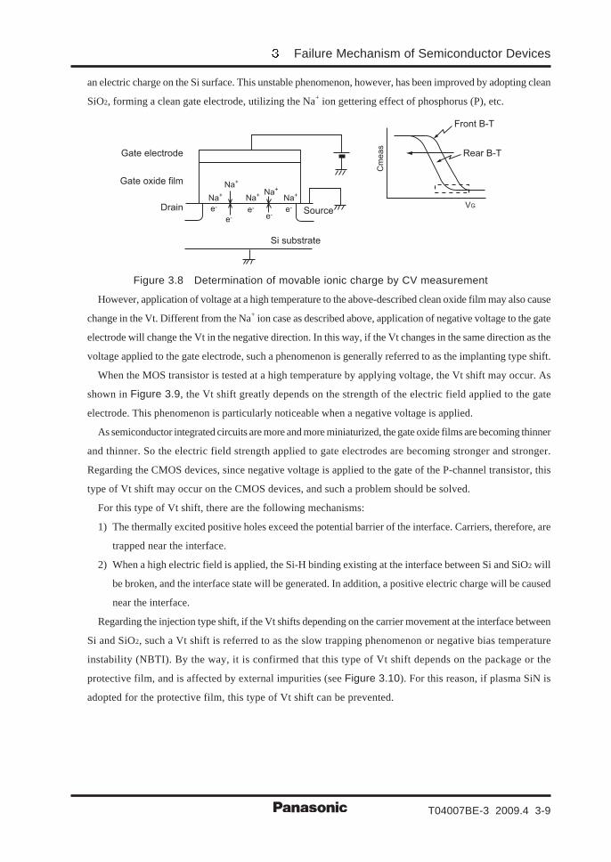
known that the following four types of electric charge can exist in gate oxide films3.1,2,3):
(1)Mobile ionic charge Qm
(2)Fixed oxide charge Qf
(3)Interface trapped charge Qit
(4)Oxide trapped charge Qot
Figure 3.7 shows the positions of these types of electric charge in the oxide film.
MOBILE IONIC
CHARGE(Qm)Na
+
K+
OXIDE TRAPPED
CHARGE(Qot) FIXED OXIDE
CHARGE(Qf)
METAL
SiO2
SiOx
Si
INTERFACE TRAPPED
CHARGE(Qit)
+-
+-
+-
+ + + + + +
Figure 3.7 Various types of electric charge in oxide film
At the early stages of MOS transistor development, application of positive voltage to the gate electrode may
greatly change the threshold voltage (Vt) value in the negative direction (see Figure 3.8). On the other hand,
application of negative voltage may slightly change the Vt value in the positive direction. This is because
application of voltage will move the Na+ ions in the gate oxide film to the interface between SiO2 and Si to cause
Failure Mechanism of Semiconductor Devices
T04007BE-3 2009.4 3-9
an electric charge on the Si surface. This unstable phenomenon, however, has been improved by adopting clean
SiO2, forming a clean gate electrode, utilizing the Na+ ion gettering effect of phosphorus (P), etc.
Na+
Na+ Na+
e-
e-e-
e-
e-
Na+Na+
Gate electrode
Gate oxide film
Drain
Si substrate
Source
Front B-T
Rear B-T
VG
Cm
eas
Figure 3.8 Determination of movable ionic charge by CV measurement
However, application of voltage at a high temperature to the above-described clean oxide film may also cause
change in the Vt. Different from the Na+ ion case as described above, application of negative voltage to the gate
electrode will change the Vt in the negative direction. In this way, if the Vt changes in the same direction as the
voltage applied to the gate electrode, such a phenomenon is generally referred to as the implanting type shift.
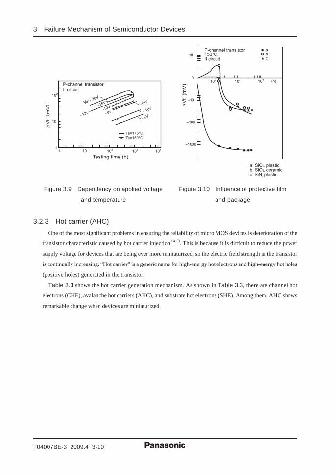
When the MOS transistor is tested at a high temperature by applying voltage, the Vt shift may occur. As
shown in Figure 3.9, the Vt shift greatly depends on the strength of the electric field applied to the gate
electrode. This phenomenon is particularly noticeable when a negative voltage is applied.
As semiconductor integrated circuits are more and more miniaturized, the gate oxide films are becoming thinner
and thinner. So the electric field strength applied to gate electrodes are becoming stronger and stronger.
Regarding the CMOS devices, since negative voltage is applied to the gate of the P-channel transistor, this
type of Vt shift may occur on the CMOS devices, and such a problem should be solved.
For this type of Vt shift, there are the following mechanisms:
1) The thermally excited positive holes exceed the potential barrier of the interface. Carriers, therefore, are
trapped near the interface.
2) When a high electric field is applied, the Si-H binding existing at the interface between Si and SiO2 will
be broken, and the interface state will be generated. In addition, a positive electric charge will be caused
near the interface.
Regarding the injection type shift, if the Vt shifts depending on the carrier movement at the interface between
Si and SiO2, such a Vt shift is referred to as the slow trapping phenomenon or negative bias temperature
instability (NBTI). By the way, it is confirmed that this type of Vt shift depends on the package or the
protective film, and is affected by external impurities (see Figure 3.10). For this reason, if plasma SiN is
adopted for the protective film, this type of Vt shift can be prevented.
3 Failure Mechanism of Semiconductor Devices
T04007BE-3 2009.4 3-10
P-channel transistorII circuit
Va: −20V
−13V
−15V
−10V
−9V
−15V
−10V
−6V
Ta=175°C
Ta=150°C
11
10
10
102
102
103 104
Testing time (h)
P-channel transistor150°CII circuit
10
0(h)
abc
102
103
104
a: SiO2, plasticb: SiO2, ceramicc: SiN, plastic
Figure 3.9 Dependency on applied voltage Figure 3.10 Influence of protective film
and temperature and package
3.2.3 Hot carrier (AHC)One of the most significant problems in ensuring the reliability of micro MOS devices is deterioration of the
transistor characteristic caused by hot carrier injection3.4,5). This is because it is difficult to reduce the power
supply voltage for devices that are being ever more miniaturized, so the electric field strength in the transistor
is continually increasing. “Hot carrier” is a generic name for high-energy hot electrons and high-energy hot holes
(positive holes) generated in the transistor.
Table 3.3 shows the hot carrier generation mechanism. As shown in Table 3.3, there are channel hot
electrons (CHE), avalanche hot carriers (AHC), and substrate hot electrons (SHE). Among them, AHC shows
remarkable change when devices are miniaturized.
Failure Mechanism of Semiconductor Devices
T04007BE-3 2009.4 3-11
Table 3.3 Hot carrier generation and bias conditions
Type
Bias condition VGS = VDS, VSX < 0
VSX Substrate(a)
DrainVDSSource
VSX
(c)
VDS
VGS
VGS = 1/2VDS, VSX < 0 VGS > 0, VDS = GND, VSX < 0
(b) Transfer gate
IN
OUT
Note: VGS = Voltage between gate and source, VDS = Voltage between drain and source, VSX = Voltage between substrate and source, = Electron, = Hole
(d) Bootstrap circuit9) (f) Capacity construction for Figure (d)
Hot carrier implanting
model
Example of a circuit that
can easily generate hot
carriers
VSX
VSX
(c)
VGS
φ
B
B
A
A
BN
Gate VGS
AHC is easily generated when the gate voltage is slightly lower than 1/2 of the drain voltage. At this point,
the carriers flowing through the channel will impact the Si crystal lattice to generate pairs of a hot electron and
a hot hole. These pairs function as hot carriers. When hot carriers are injected into a gate oxide film, the gate
oxide film may be charged, or the Si-SiO2 interface may be damaged. As a result, the transistor characteristic
may be changed. The amount of hot carriers implanted into the gate oxide film cannot be directly measured,
but can be indirectly assumed from the substrate current (current of hot holes generated by impact ionization).
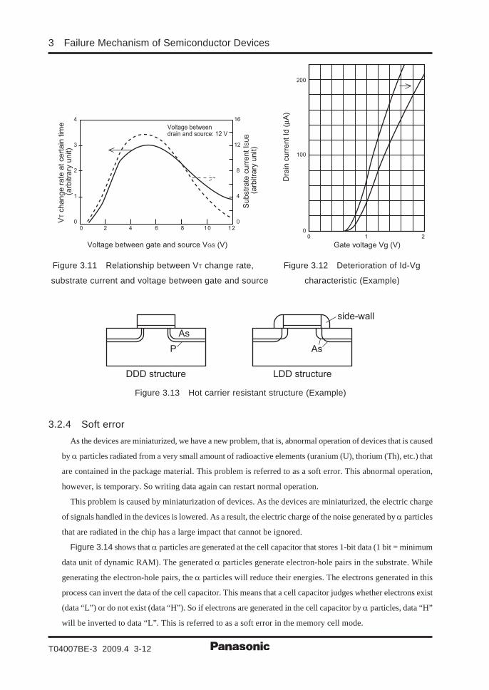
Figure 3.11 shows the relationship between the VT change rate, the substrate current, and the voltage between
gate and source when the VDS is constant. As shown in Figure 3.11, when the VDS value is almost twice as
much as the VGS value (2VGS = VDS), the substrate current will be maximized. At this point, the AHC shows
a remarkable characteristic change. To carry out a test, the gate voltage is generally set to the point where the
substrate current can be maximized.
Hot carriers injection into a gate oxide film may generate the interface state and fixed charge, and may
finally deteriorate the Vt and the gm of the FET. Figure 3.12 shows deterioration of the Id-Vg characteristic
of the transistor as an example. As shown in the figure, as the Vt of the FET is increased, the circuit operation
will become slow, and will finally operate abnormally (see Figure 3.13).
To improve the resistance to hot carriers, a special transistor structure (LDD) is adopted for recent micro-
device processes because this special transistor structure can lower the electric field near the drain.
3 Failure Mechanism of Semiconductor Devices
T04007BE-3 2009.4 3-12
Gate voltage Vg (V)
Dra
in c
urr
en
t Id
(μA
)
Voltage between drain and source: 12 V
16
12
8
4
0
4
3
2
1
00 2 4 6 8 10 12
Voltage between gate and source VGS (V)
VT c
ha
ng
e r
ate
at
ce
rta
in t
ime
(a
rbitra
ry u
nit)
Su
bstr
ate
cu
rre
nt
ISU
B
(arb
itra
ry u
nit)
20 10
100
200
Figure 3.11 Relationship between VT change rate, Figure 3.12 Deterioration of Id-Vg
substrate current and voltage between gate and source characteristic (Example)
As
DDD structure LDD structure
P As
side-wall
Figure 3.13 Hot carrier resistant structure (Example)
3.2.4 Soft errorAs the devices are miniaturized, we have a new problem, that is, abnormal operation of devices that is caused
by α particles radiated from a very small amount of radioactive elements (uranium (U), thorium (Th), etc.) that
are contained in the package material. This problem is referred to as a soft error. This abnormal operation,
however, is temporary. So writing data again can restart normal operation.
This problem is caused by miniaturization of devices. As the devices are miniaturized, the electric charge
of signals handled in the devices is lowered. As a result, the electric charge of the noise generated by α particles
that are radiated in the chip has a large impact that cannot be ignored.
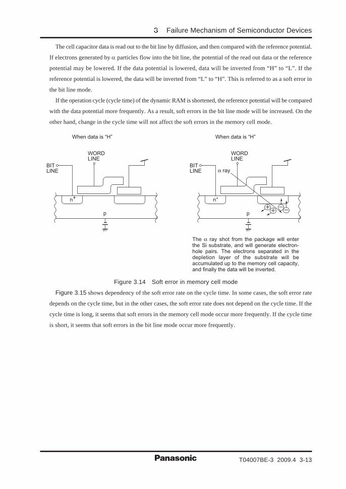
Figure 3.14 shows that α particles are generated at the cell capacitor that stores 1-bit data (1 bit = minimum
data unit of dynamic RAM). The generated α particles generate electron-hole pairs in the substrate. While
generating the electron-hole pairs, the α particles will reduce their energies. The electrons generated in this
process can invert the data of the cell capacitor. This means that a cell capacitor judges whether electrons exist
(data “L”) or do not exist (data “H”). So if electrons are generated in the cell capacitor by α particles, data “H”
will be inverted to data “L”. This is referred to as a soft error in the memory cell mode.
Failure Mechanism of Semiconductor Devices
T04007BE-3 2009.4 3-13
The cell capacitor data is read out to the bit line by diffusion, and then compared with the reference potential.
If electrons generated by α particles flow into the bit line, the potential of the read out data or the reference
potential may be lowered. If the data potential is lowered, data will be inverted from “H” to “L”. If the
reference potential is lowered, the data will be inverted from “L” to “H”. This is referred to as a soft error in
the bit line mode.
If the operation cycle (cycle time) of the dynamic RAM is shortened, the reference potential will be compared
with the data potential more frequently. As a result, soft errors in the bit line mode will be increased. On the
other hand, change in the cycle time will not affect the soft errors in the memory cell mode.
BITLINE
WORDLINE
n+
p
BITLINE
WORDLINE
n+
p
The α ray shot from the package will enter the Si substrate, and will generate electron-hole pairs. The electrons separated in the depletion layer of the substrate will be accumulated up to the memory cell capacity, and finally the data will be inverted.
α ray
When data is “H” When data is “H”
Figure 3.14 Soft error in memory cell mode
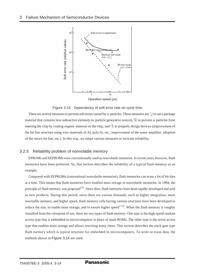
Figure 3.15 shows dependency of the soft error rate on the cycle time. In some cases, the soft error rate
depends on the cycle time, but in the other cases, the soft error rate does not depend on the cycle time. If the
cycle time is long, it seems that soft errors in the memory cell mode occur more frequently. If the cycle time
is short, it seems that soft errors in the bit line mode occur more frequently.
3 Failure Mechanism of Semiconductor Devices
T04007BE-3 2009.4 3-14
Memory cell mode("H"→"L")
Soft errors in experiment
Bit line mode("L"→"H")
Operation speed (μs)
Soft e
rror
rate
(re
lative v
alu
e)
1
101
102
103
10
Figure 3.15 Dependency of soft error rate on cycle time
There are several measures to prevent soft errors caused by α particles. These measures are to use a package
material that contains less radioactive elements (α particle generative source), to prevent α particles from
entering the chip by coating organic material on the chip, and to properly design devices (improvement of
the bit line structure using wire materials of Al, poly-Si, etc., improvement of the sense amplifier, adoption
of the return bit line, etc.). In this way, we adopt various measures to increase reliability.
3.2.5 Reliability problem of nonvolatile memoryEPROMs and EEPROMs were conventionally used as nonvolatile memories. In recent years, however, flash
memories have been preferred. So, this section describes the reliability of a typical flash memory as an
example.
Compared with EEPROMs (conventional nonvolatile memories), flash memories can erase a lot of bit data
at a time. This means that flash memories have enabled mass storage in nonvolatile memories. In 1984, the
principle of flash memory was proposed3.6). Since then, flash memories have been rapidly developed and sold
as new products. During this period, since there are various demands, such as higher integration, more
rewritable memory, and higher speed, flash memory cells having various structures have been developed to
reduce the size, to enable mass storage, and to ensure higher speed3.7,8). When the flash memory is roughly
classified from the viewpoint of use, there are two types of flash memory. One type is the high-speed random
access type that is embedded in microcomputers in place of mask ROMs. The other type is the serial access
type that enables mass storage and allows rewriting many times. This section describes the stack gate type
flash memory which is typical structure for embedded in microcomputers. To write or erase data, the
methods shown in Figure 3.16 are used.
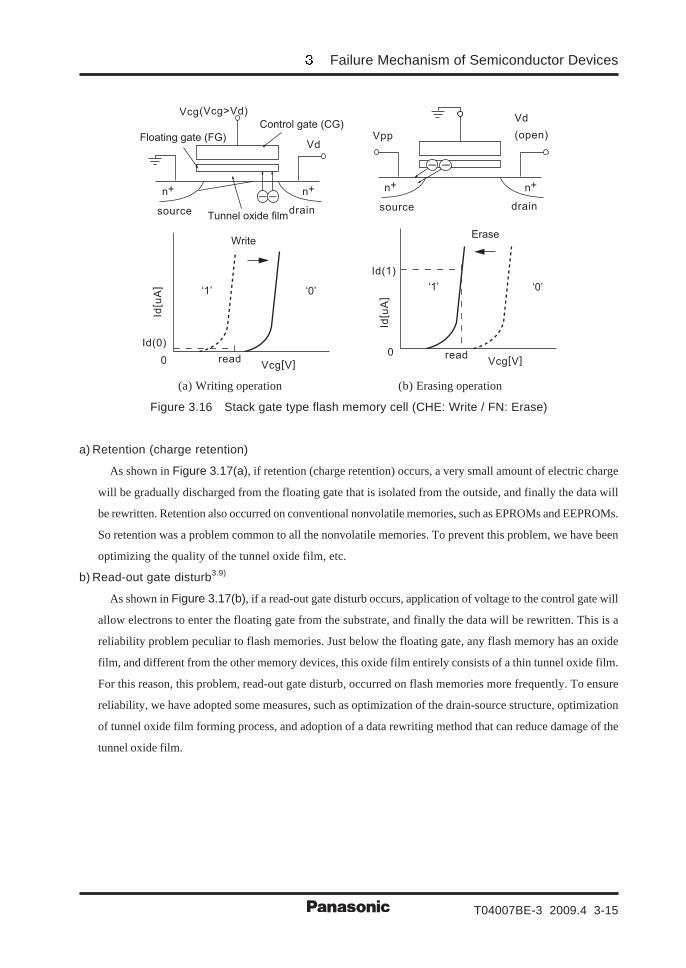
Failure Mechanism of Semiconductor Devices
T04007BE-3 2009.4 3-15
read
drainsource
n+ n+
Id(1)
Vcg[V]
Id[ u
A]
Vd
(open)Vpp
0
Erase
read
drainsource
n+ n+
Id(0)
Vcg[V]
Id[ u
A]
Vcg(Vcg>Vd)
Vd
0
Write
Tunnel oxide film
Control gate (CG)
Floating gate (FG)
‘1’ ‘0’ ‘1’ ‘0’
(a) Writing operation (b) Erasing operation
Figure 3.16 Stack gate type flash memory cell (CHE: Write / FN: Erase)
a) Retention (charge retention)
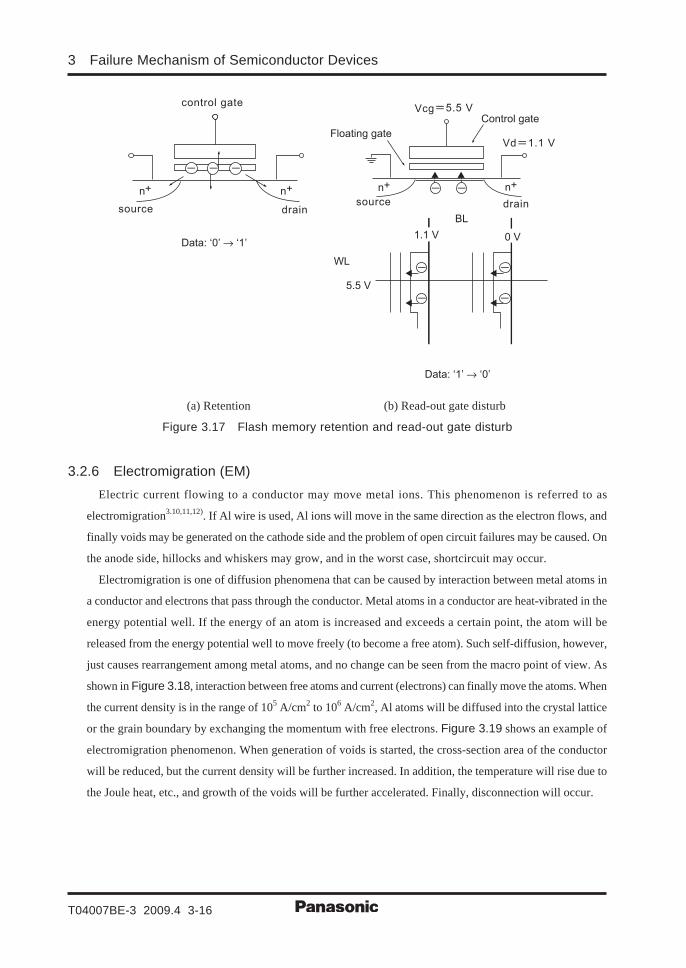
As shown in Figure 3.17(a), if retention (charge retention) occurs, a very small amount of electric charge
will be gradually discharged from the floating gate that is isolated from the outside, and finally the data will
be rewritten. Retention also occurred on conventional nonvolatile memories, such as EPROMs and EEPROMs.
So retention was a problem common to all the nonvolatile memories. To prevent this problem, we have been
optimizing the quality of the tunnel oxide film, etc.
b) Read-out gate disturb3.9)
As shown in Figure 3.17(b), if a read-out gate disturb occurs, application of voltage to the control gate will
allow electrons to enter the floating gate from the substrate, and finally the data will be rewritten. This is a
reliability problem peculiar to flash memories. Just below the floating gate, any flash memory has an oxide
film, and different from the other memory devices, this oxide film entirely consists of a thin tunnel oxide film.
For this reason, this problem, read-out gate disturb, occurred on flash memories more frequently. To ensure
reliability, we have adopted some measures, such as optimization of the drain-source structure, optimization
of tunnel oxide film forming process, and adoption of a data rewriting method that can reduce damage of the
tunnel oxide film.
3 Failure Mechanism of Semiconductor Devices
T04007BE-3 2009.4 3-16
drainsource
n+ n+
Vcg 5.5 V
Vd 1.1 V
Control gate
Floating gate
Data: ‘0’ → ‘1’
Data: ‘1’ → ‘0’
drainsource
n+ n+
control gate
BL
WL
1.1 V
5.5 V
0 V
(a) Retention (b) Read-out gate disturb
Figure 3.17 Flash memory retention and read-out gate disturb
3.2.6 Electromigration (EM)Electric current flowing to a conductor may move metal ions. This phenomenon is referred to as
electromigration3.10,11,12). If Al wire is used, Al ions will move in the same direction as the electron flows, and
finally voids may be generated on the cathode side and the problem of open circuit failures may be caused. On
the anode side, hillocks and whiskers may grow, and in the worst case, shortcircuit may occur.
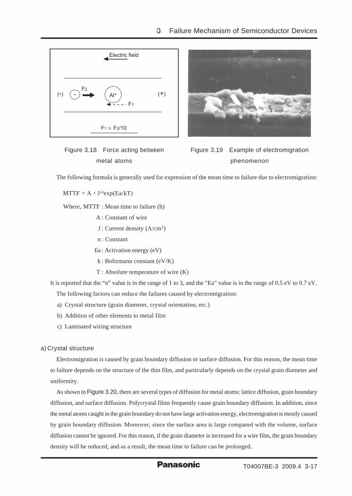
Electromigration is one of diffusion phenomena that can be caused by interaction between metal atoms in
a conductor and electrons that pass through the conductor. Metal atoms in a conductor are heat-vibrated in the
energy potential well. If the energy of an atom is increased and exceeds a certain point, the atom will be
released from the energy potential well to move freely (to become a free atom). Such self-diffusion, however,
just causes rearrangement among metal atoms, and no change can be seen from the macro point of view. As
shown in Figure 3.18, interaction between free atoms and current (electrons) can finally move the atoms. When
the current density is in the range of 105 A/cm2 to 106 A/cm2, Al atoms will be diffused into the crystal lattice
or the grain boundary by exchanging the momentum with free electrons. Figure 3.19 shows an example of
electromigration phenomenon. When generation of voids is started, the cross-section area of the conductor
will be reduced, but the current density will be further increased. In addition, the temperature will rise due to
the Joule heat, etc., and growth of the voids will be further accelerated. Finally, disconnection will occur.
Failure Mechanism of Semiconductor Devices
T04007BE-3 2009.4 3-17
Electric field
F1
Al+F2
F1 F2/10
(-) - (+)
Figure 3.18 Force acting between Figure 3.19 Example of electromigration
metal atoms phenomenon
The following formula is generally used for expression of the mean time to failure due to electromigration:
MTTF = A J-nexp(Ea/kT)
Where, MTTF : Mean time to failure (h)
A : Constant of wire
J : Current density (A/cm2)
n : Constant
Ea : Activation energy (eV)
k : Boltzmann constant (eV/K)
T : Absolute temperature of wire (K)
It is reported that the “n” value is in the range of 1 to 3, and the “Ea” value is in the range of 0.5 eV to 0.7 eV.
The following factors can reduce the failures caused by electromigration:
a) Crystal structure (grain diameter, crystal orientation, etc.)
b) Addition of other elements to metal film
c) Laminated wiring structure
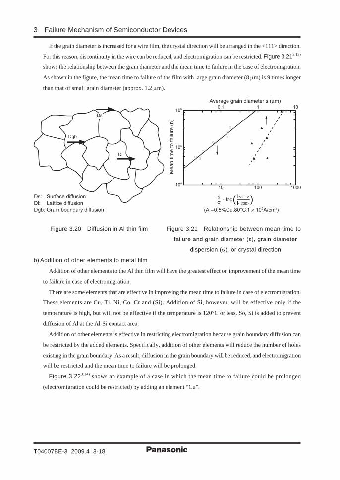
a) Crystal structure
Electromigration is caused by grain boundary diffusion or surface diffusion. For this reason, the mean time
to failure depends on the structure of the thin film, and particularly depends on the crystal grain diameter and
uniformity.
As shown in Figure 3.20, there are several types of diffusion for metal atoms: lattice diffusion, grain boundary
diffusion, and surface diffusion. Polycrystal films frequently cause grain boundary diffusion. In addition, since
the metal atoms caught in the grain boundary do not have large activation energy, electromigration is mostly caused
by grain boundary diffusion. Moreover, since the surface area is large compared with the volume, surface
diffusion cannot be ignored. For this reason, if the grain diameter is increased for a wire film, the grain boundary
density will be reduced, and as a result, the mean time to failure can be prolonged.
3 Failure Mechanism of Semiconductor Devices
T04007BE-3 2009.4 3-18
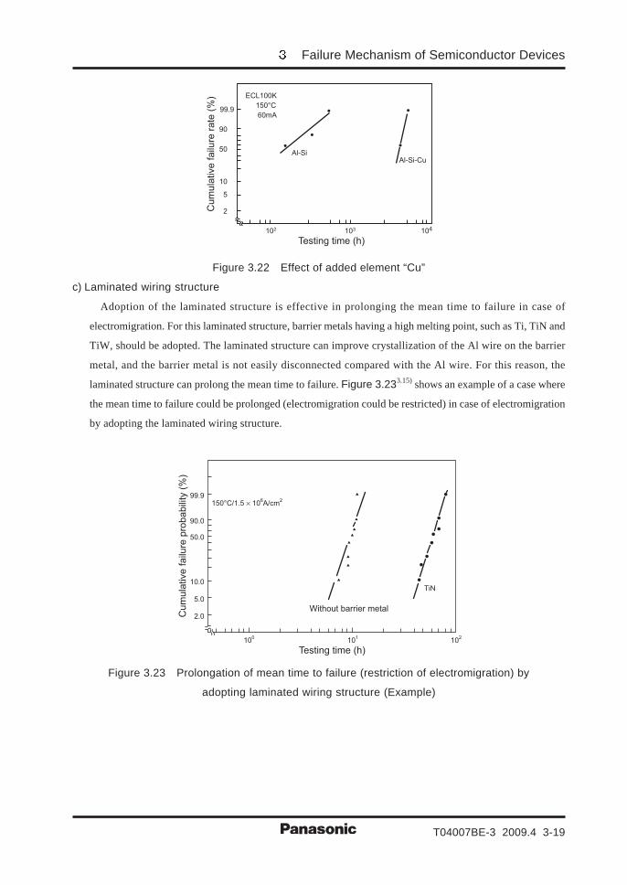
If the grain diameter is increased for a wire film, the crystal direction will be arranged in the <111> direction.
For this reason, discontinuity in the wire can be reduced, and electromigration can be restricted. Figure 3.213.13)
shows the relationship between the grain diameter and the mean time to failure in the case of electromigration.
As shown in the figure, the mean time to failure of the film with large grain diameter (8 μm) is 9 times longer
than that of small grain diameter (approx. 1.2 μm).
Ds
Dgb
Dl
· log( )sσ
I<111>
I<200>
(Al-0.5%Cu,80°C,1 × 105A/cm2)
Average grain diameter s (μm)
Mean tim
e to failu
re (
h)
10104
105
1060.1 1 10
100 1000
Ds: Surface diffusion
Dl: Lattice diffusion
Dgb: Grain boundary diffusion
Figure 3.20 Diffusion in Al thin film Figure 3.21 Relationship between mean time to
failure and grain diameter (s), grain diameter
dispersion (σ), or crystal direction
b) Addition of other elements to metal film
Addition of other elements to the Al thin film will have the greatest effect on improvement of the mean time
to failure in case of electromigration.
There are some elements that are effective in improving the mean time to failure in case of electromigration.
These elements are Cu, Ti, Ni, Co, Cr and (Si). Addition of Si, however, will be effective only if the
temperature is high, but will not be effective if the temperature is 120°C or less. So, Si is added to prevent
diffusion of Al at the Al-Si contact area.
Addition of other elements is effective in restricting electromigration because grain boundary diffusion can
be restricted by the added elements. Specifically, addition of other elements will reduce the number of holes
existing in the grain boundary. As a result, diffusion in the grain boundary will be reduced, and electromigration
will be restricted and the mean time to failure will be prolonged.
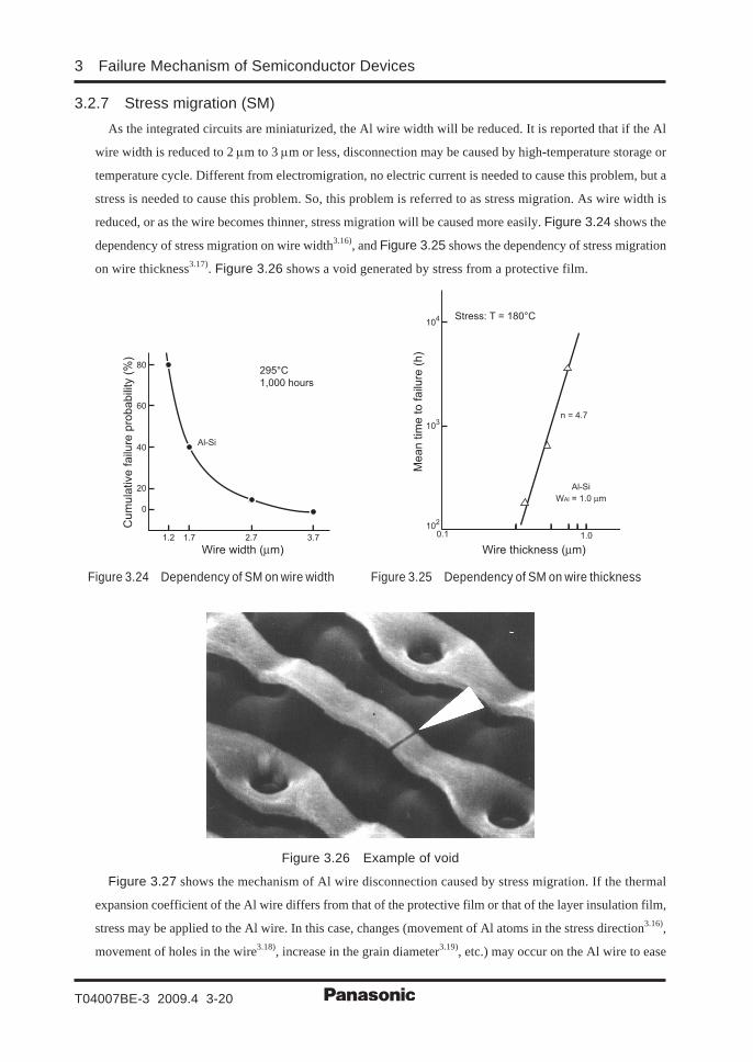
Figure 3.223.14) shows an example of a case in which the mean time to failure could be prolonged
(electromigration could be restricted) by adding an element “Cu”.
Failure Mechanism of Semiconductor Devices
T04007BE-3 2009.4 3-19
ECL100K
150°C
60mA
Al-SiAl-Si-Cu
Testing time (h)
Cum
ula
tive failu
re r
ate
(%
)
99.9
90
50
10
5
2
102 103 104
Figure 3.22 Effect of added element “Cu”
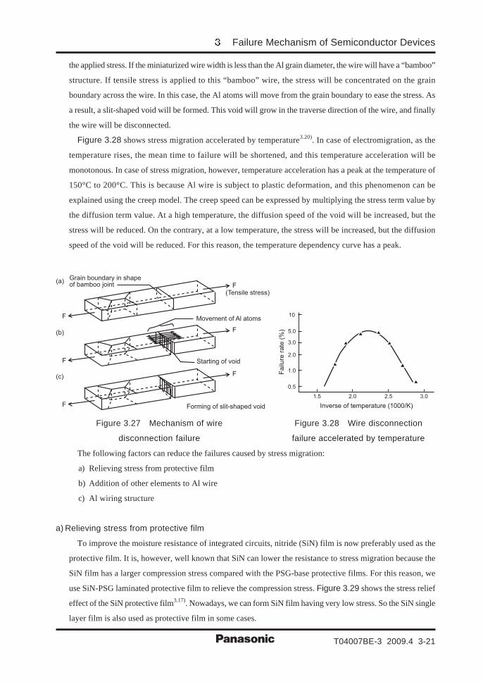
c) Laminated wiring structure
Adoption of the laminated structure is effective in prolonging the mean time to failure in case of
electromigration. For this laminated structure, barrier metals having a high melting point, such as Ti, TiN and
TiW, should be adopted. The laminated structure can improve crystallization of the Al wire on the barrier
metal, and the barrier metal is not easily disconnected compared with the Al wire. For this reason, the
laminated structure can prolong the mean time to failure. Figure 3.233.15) shows an example of a case where
the mean time to failure could be prolonged (electromigration could be restricted) in case of electromigration
by adopting the laminated wiring structure.
100
101
102
2.0
5.0
10.0
99.9
90.0
50.0
Testing time (h)
Cum
ula
tive
failu
re p
robabili
ty (
%)
Without barrier metal
TiN
150°C/1.5 × 106A/cm
2
Figure 3.23 Prolongation of mean time to failure (restriction of electromigration) by
adopting laminated wiring structure (Example)
3 Failure Mechanism of Semiconductor Devices
T04007BE-3 2009.4 3-20
3.2.7 Stress migration (SM)As the integrated circuits are miniaturized, the Al wire width will be reduced. It is reported that if the Al
wire width is reduced to 2 μm to 3 μm or less, disconnection may be caused by high-temperature storage or
temperature cycle. Different from electromigration, no electric current is needed to cause this problem, but a
stress is needed to cause this problem. So, this problem is referred to as stress migration. As wire width is
reduced, or as the wire becomes thinner, stress migration will be caused more easily. Figure 3.24 shows the
dependency of stress migration on wire width3.16), and Figure 3.25 shows the dependency of stress migration
on wire thickness3.17). Figure 3.26 shows a void generated by stress from a protective film.
Al-Si
295°C
1,000 hours
Wire width (μm)
Cu
mu
lative
fa
ilure
pro
ba
bili
ty (
%)
1.2
80
60
40
20
0
1.7 2.7 3.7
Wire thickness (μm)
Me
an
tim
e t
o f
ailu
re (
h)
104
103
102
1.00.1
Stress: T = 180°C
n = 4.7
Al-Si
WAl = 1.0 μm
Figure 3.24 Dependency of SM on wire width Figure 3.25 Dependency of SM on wire thickness
Figure 3.26 Example of void
Figure 3.27 shows the mechanism of Al wire disconnection caused by stress migration. If the thermal
expansion coefficient of the Al wire differs from that of the protective film or that of the layer insulation film,
stress may be applied to the Al wire. In this case, changes (movement of Al atoms in the stress direction3.16),
movement of holes in the wire3.18), increase in the grain diameter3.19), etc.) may occur on the Al wire to ease
Failure Mechanism of Semiconductor Devices
T04007BE-3 2009.4 3-21
the applied stress. If the miniaturized wire width is less than the Al grain diameter, the wire will have a “bamboo”
structure. If tensile stress is applied to this “bamboo” wire, the stress will be concentrated on the grain
boundary across the wire. In this case, the Al atoms will move from the grain boundary to ease the stress. As
a result, a slit-shaped void will be formed. This void will grow in the traverse direction of the wire, and finally
the wire will be disconnected.
Figure 3.28 shows stress migration accelerated by temperature3.20). In case of electromigration, as the
temperature rises, the mean time to failure will be shortened, and this temperature acceleration will be
monotonous. In case of stress migration, however, temperature acceleration has a peak at the temperature of
150°C to 200°C. This is because Al wire is subject to plastic deformation, and this phenomenon can be
explained using the creep model. The creep speed can be expressed by multiplying the stress term value by
the diffusion term value. At a high temperature, the diffusion speed of the void will be increased, but the
stress will be reduced. On the contrary, at a low temperature, the stress will be increased, but the diffusion
speed of the void will be reduced. For this reason, the temperature dependency curve has a peak.
Grain boundary in shape of bamboo joint
(a)
F
F(Tensile stress)
Movement of Al atoms
Starting of void
(b)
F
F
Forming of slit-shaped void
(c)
F
F
1.5
10
5.0
3.0
2.0
1.0
0.5
2.0 2.5
Inverse of temperature (1000/K)
Failu
re r
ate
(%
)
3.0
Figure 3.27 Mechanism of wire Figure 3.28 Wire disconnection
disconnection failure failure accelerated by temperature
The following factors can reduce the failures caused by stress migration:
a) Relieving stress from protective film
b) Addition of other elements to Al wire
c) Al wiring structure
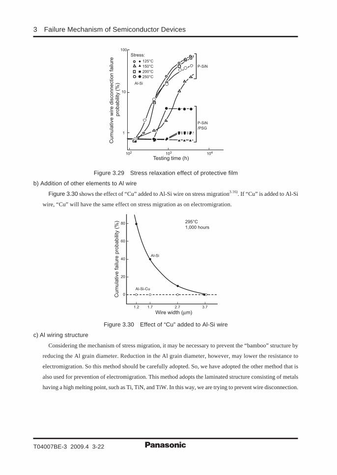
a) Relieving stress from protective film
To improve the moisture resistance of integrated circuits, nitride (SiN) film is now preferably used as the
protective film. It is, however, well known that SiN can lower the resistance to stress migration because the
SiN film has a larger compression stress compared with the PSG-base protective films. For this reason, we
use SiN-PSG laminated protective film to relieve the compression stress. Figure 3.29 shows the stress relief
effect of the SiN protective film3.17). Nowadays, we can form SiN film having very low stress. So the SiN single
layer film is also used as protective film in some cases.
3 Failure Mechanism of Semiconductor Devices
T04007BE-3 2009.4 3-22
Stress:
125°C
150°C
200°C
250°C
Al-Si
P-SiN
P-SiN
/PSG
102
1
10
100
103 104
Testing time (h)
Cum
ula
tive w
ire d
isconnection failu
re
pro
babili
ty (
%)
Figure 3.29 Stress relaxation effect of protective film
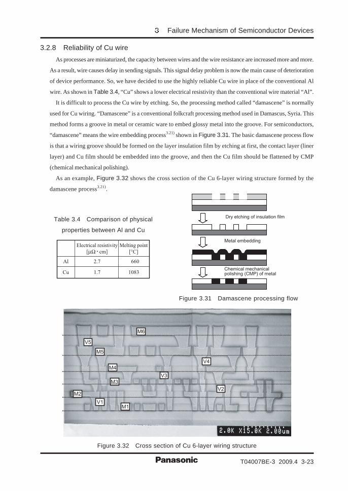
b) Addition of other elements to Al wire
Figure 3.30 shows the effect of “Cu” added to Al-Si wire on stress migration3.16). If “Cu” is added to Al-Si
wire, “Cu” will have the same effect on stress migration as on electromigration.
Cum
ula
tive failu
re p
robabili
ty (
%)
Wire width (μm)
80
0
20
1.2 1.7 2.7 3.7
40
60
Al-Si
Al-Si-Cu
295°C
1,000 hours
Figure 3.30 Effect of “Cu” added to Al-Si wire
c) Al wiring structure
Considering the mechanism of stress migration, it may be necessary to prevent the “bamboo” structure by
reducing the Al grain diameter. Reduction in the Al grain diameter, however, may lower the resistance to
electromigration. So this method should be carefully adopted. So, we have adopted the other method that is
also used for prevention of electromigration. This method adopts the laminated structure consisting of metals
having a high melting point, such as Ti, TiN, and TiW. In this way, we are trying to prevent wire disconnection.
Failure Mechanism of Semiconductor Devices
T04007BE-3 2009.4 3-23
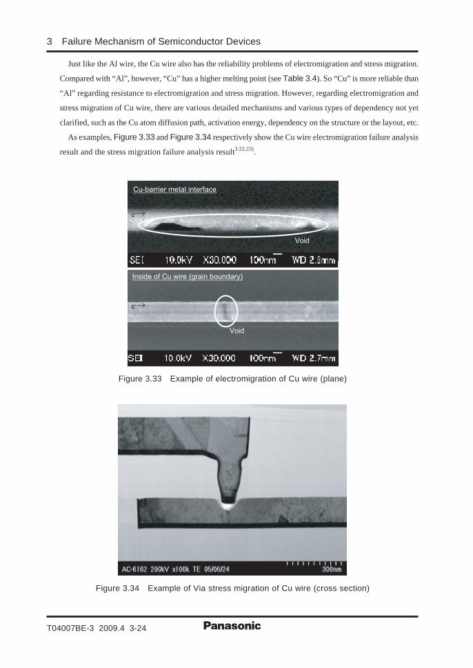
3.2.8 Reliability of Cu wireAs processes are miniaturized, the capacity between wires and the wire resistance are increased more and more.
As a result, wire causes delay in sending signals. This signal delay problem is now the main cause of deterioration
of device performance. So, we have decided to use the highly reliable Cu wire in place of the conventional Al
wire. As shown in Table 3.4, “Cu” shows a lower electrical resistivity than the conventional wire material “Al”.
It is difficult to process the Cu wire by etching. So, the processing method called “damascene” is normally
used for Cu wiring. “Damascene” is a conventional folkcraft processing method used in Damascus, Syria. This
method forms a groove in metal or ceramic ware to embed glossy metal into the groove. For semiconductors,
“damascene” means the wire embedding process3.21) shown in Figure 3.31. The basic damascene process flow
is that a wiring groove should be formed on the layer insulation film by etching at first, the contact layer (liner
layer) and Cu film should be embedded into the groove, and then the Cu film should be flattened by CMP
(chemical mechanical polishing).
As an example, Figure 3.32 shows the cross section of the Cu 6-layer wiring structure formed by the
damascene process3.21).
Table 3.4 Comparison of physical
properties between Al and Cu
Al
Cu
2.7
1.7
660
1083
Electrical resistivity
[μΩ • cm]
Melting point
[°C]
Chemical mechanical polishing (CMP) of metal
Metal embedding
Dry etching of insulation film
Figure 3.31 Damascene processing flow
M1
M2
M3
M4
M5
M6
V1
V2
V3
V4
V5
M1
M2
M3
M4
M5
M6
V1
V2
V3
V4
V5
Figure 3.32 Cross section of Cu 6-layer wiring structure
3 Failure Mechanism of Semiconductor Devices
T04007BE-3 2009.4 3-24
Just like the Al wire, the Cu wire also has the reliability problems of electromigration and stress migration.
Compared with “Al”, however, “Cu” has a higher melting point (see Table 3.4). So “Cu” is more reliable than
“Al” regarding resistance to electromigration and stress migration. However, regarding electromigration and
stress migration of Cu wire, there are various detailed mechanisms and various types of dependency not yet
clarified, such as the Cu atom diffusion path, activation energy, dependency on the structure or the layout, etc.
As examples, Figure 3.33 and Figure 3.34 respectively show the Cu wire electromigration failure analysis
result and the stress migration failure analysis result3.22,23).
Cu-barrier metal interface
Inside of Cu wire (grain boundary)
Void
Void
e-→
e-→
Figure 3.33 Example of electromigration of Cu wire (plane)
Figure 3.34 Example of Via stress migration of Cu wire (cross section)
Failure Mechanism of Semiconductor Devices
T04007BE-3 2009.4 3-25
3.2.9 Al corrosionVarious types of resin sealed packages are used in various fields. Resin, however, is moisture absorbent and
moisture permeable, and contains a small amount of Cl and Na that can be easily ionized by water. If a halogen
substance in the flux, such as Cl or F, enters a package, and if the ambient condition is humid, the leakage
current may be increased, characteristics may be deteriorated (withstand voltage may be lowered, etc.), or
wire breakage may occur due to Al wire corrosion3.24).
a) Moisture path
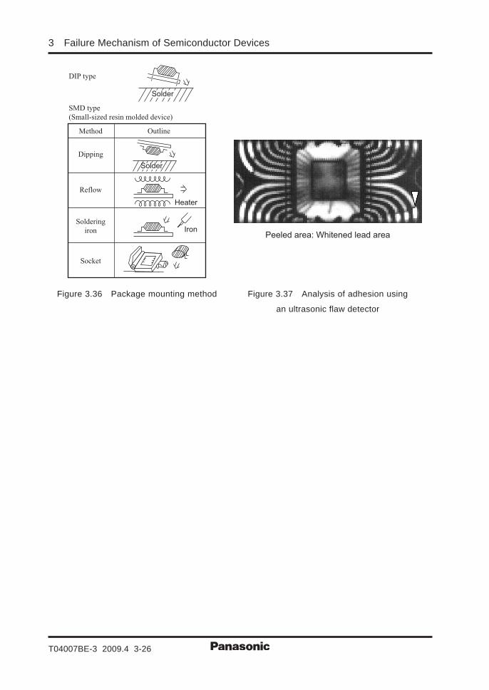
As shown in Figure 3.35, moisture can enter a resin sealed package using two paths. One is the path that
leads to the inside of the resin bulk, and the other is the path that passes through the interface between the
lead frame and the resin. One of these paths will become the main path, and which will become the main path
greatly depends on the resin material and the lead frame material.
On the other hand, as packages are miniaturized, the surface mounting method is subject to change as
shown in Figure 3.36. Due to change in the surface mounting method, the entire surface of each package is
now exposed to a higher temperature compared with the conventional packages, as shown in Figure 3.36. So,
there is possibility that the adhesion between the lead frame and the resin may be deteriorated. Figure 3.37
shows the result of an examination of deterioration of the adhesion between the lead frame and the resin using
an ultrasonic flaw detector after solder dipping. As you can see from the figure, thermal stress applied during
surface mounting may occasionally cause adhesion deterioration.
Bonded wireChip
Moisture permeation into resin
Resin
Moisture permeation through interface Lead
Figure 3.35 Moisture path
3 Failure Mechanism of Semiconductor Devices
T04007BE-3 2009.4 3-26
Solder
Solder
Heater
Iron
SMD type
(Small-sized resin molded device)
DIP type
Method Outline
Dipping
Reflow
Soldering
iron
Socket
Peeled area: Whitened lead area
Figure 3.36 Package mounting method Figure 3.37 Analysis of adhesion using
an ultrasonic flaw detector
Failure Mechanism of Semiconductor Devices
T04007BE-3 2009.4 3-27
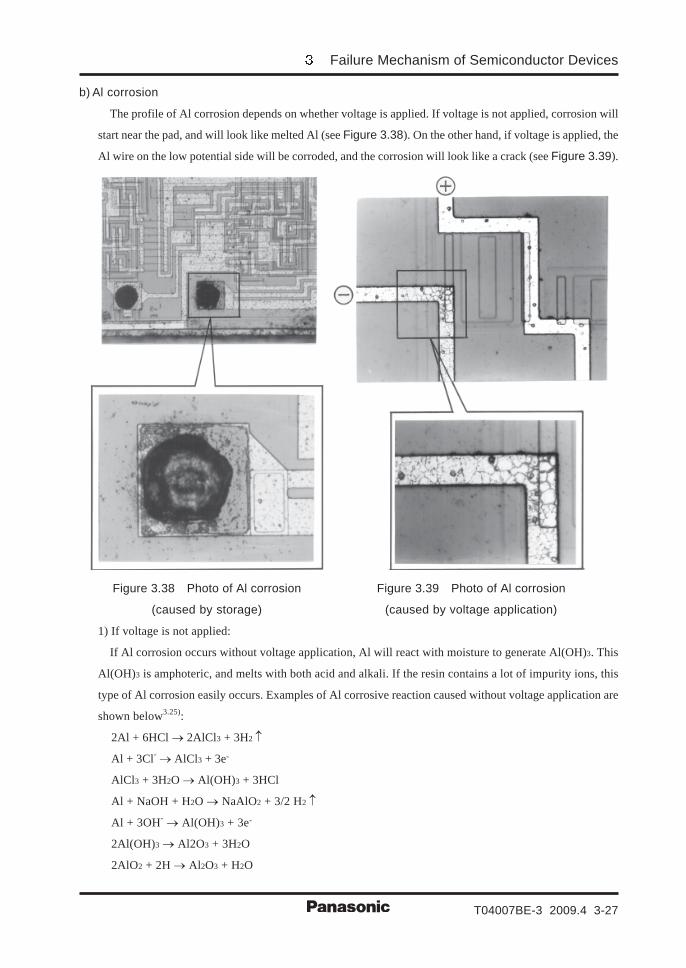
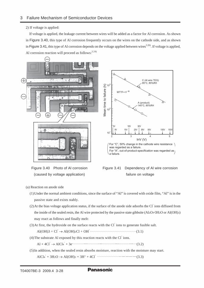
b) Al corrosion
The profile of Al corrosion depends on whether voltage is applied. If voltage is not applied, corrosion will
start near the pad, and will look like melted Al (see Figure 3.38). On the other hand, if voltage is applied, the
Al wire on the low potential side will be corroded, and the corrosion will look like a crack (see Figure 3.39).
Figure 3.38 Photo of Al corrosion Figure 3.39 Photo of Al corrosion
(caused by storage) (caused by voltage application)
1) If voltage is not applied:
If Al corrosion occurs without voltage application, Al will react with moisture to generate Al(OH)3. This
Al(OH)3 is amphoteric, and melts with both acid and alkali. If the resin contains a lot of impurity ions, this
type of Al corrosion easily occurs. Examples of Al corrosive reaction caused without voltage application are
shown below3.25):
2Al + 6HCl → 2AlCl3 + 3H2 ↑
Al + 3Cl- → AlCl3 + 3e-
AlCl3 + 3H2O → Al(OH)3 + 3HCl
Al + NaOH + H2O → NaAlO2 + 3/2 H2 ↑
Al + 3OH- → Al(OH)3 + 3e-
2Al(OH)3 → Al2O3 + 3H2O
2AlO2 + 2H → Al2O3 + H2O
3 Failure Mechanism of Semiconductor Devices
T04007BE-3 2009.4 3-28
2) If voltage is applied:
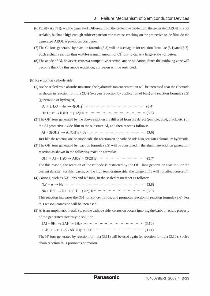
If voltage is applied, the leakage current between wires will be added as a factor for Al corrosion. As shown
in Figure 3.40, this type of Al corrosion frequently occurs on the wires on the cathode side, and as shown
in Figure 3.41, this type of Al corrosion depends on the voltage applied between wires3.26). If voltage is applied,
Al corrosion reaction will proceed as follows:3.24)
3V 18V 30V
9V 15V 25V 36V 50V 100V 150V
2
101
102
103
C (Al wire TEG)85°C, 85%RH
A (product)140°C, 85%RH
InV (V)3 4 5
MTTF∝V−a
Mean tim
e to failu
re (
h)
For “C”, 50% change in the cathode wire resistance was regarded as a failure.
For “A”, out-of-product-specification was regarded as a failure.
Figure 3.40 Photo of Al corrosion Figure 3.41 Dependency of Al wire corrosion
(caused by voltage application) failure on voltage
(a) Reaction on anode side
(1)Under the normal ambient conditions, since the surface of “Al” is covered with oxide film, “Al” is in the
passive state and exists stably.
(2)At the bias voltage application status, if the surface of the anode side adsorbs the Cl- ions diffused from
the inside of the sealed resin, the Al wire protected by the passive state gibbsite (Al2O3•3H2O or Al(OH)3)
may react as follows and finally melt:
(3)At first, the hydroxide on the surface reacts with the Cl- ions to generate fusible salt.
Al(OH)3 + Cl- → Al(OH)2Cl + OH- (3.1)
(4)The substrate Al exposed by this reaction reacts with the Cl- ions.
Al + 4Cl- → AlCl4- + 3e- (3.2)
(5)In addition, when the sealed resin absorbs moisture, reaction with the moisture may start.
AlCl4- + 3H2O → Al(OH)3 + 3H+ + 4Cl- (3.3)
Failure Mechanism of Semiconductor Devices
T04007BE-3 2009.4 3-29
(6)Finally Al(OH)3 will be generated. Different from the protective oxide film, the generated Al(OH)3 is not
sealable, but has a high enough cubic expansion rate to cause cracking on the protective oxide film. So the
generated Al(OH)3 promotes corrosion.
(7)The Cl- ions generated by reaction formula (3.3) will be used again for reaction formulae (3.1) and (3.2).
Such a chain reaction thus enables a small amount of Cl- ions to cause a large-scale corrosion.
(8)The anode of Al, however, causes a competitive reaction: anode oxidation. Since the oxidizing zone will
become thick by this anode oxidation, corrosion will be restricted.
(b) Reaction on cathode side
(1)As the sealed resin absorbs moisture, the hydroxide ion concentration will be increased near the electrode
as shown in reaction formula (3.4) (oxygen reduction by application of bias) and reaction formula (3.5)
(generation of hydrogen).
O2 + 2H2O + 4e- → 4(OH)- (3.4)
H2O + e- → (OH)- + (1/2)H2 (3.5)
(2)The OH- ions generated by the above reaction are diffused from the defect (pinhole, void, crack, etc.) on
the Al protective oxide film to the substrate Al, and then react as follows:
Al + 3(OH)- → Al(OH)3 + 3e- (3.6)
Just like the reaction on the anode side, the reaction on he cathode side also generates aluminum hydroxide.
(3)The OH- ions generated by reaction formula (3.5) will be consumed in the aluminate acid ion generation
reaction as shown in the following reaction formula:
OH- + Al + H2O → AlO2- + (3/2)H2 (3.7)
For this reason, the reaction of the cathode is restricted by the OH- ions generation reaction, or the
current density. For this reason, on the high temperature side, the temperature will not affect corrosion.
(4)Cations, such as Na+ ions and K+ ions, in the sealed resin react as follows:
Na+ + e- → Na (3.8)
Na + H2O → Na+ + OH- + (1/2)H2 (3.9)
This reaction increases the OH- ion concentration, and promotes reaction in reaction formula (3.6). For
this reason, corrosion will be increased.
(5)Al is an amphoteric metal. So, on the cathode side, corrosion occurs ignoring the basic or acidic property
of the generated electrolytic solution.
2Al + 6H+ → 2Al3+ + 3H2 (3.10)
2Al3+ + 6H2O → 2Al(OH)3 + 6H+ (3.11)
The H+ ions generated by reaction formula (3.11) will be used again for reaction formula (3.10). Such a
chain reaction thus promotes corrosion.
3 Failure Mechanism of Semiconductor Devices
T04007BE-3 2009.4 3-30
c) Characteristic deterioration
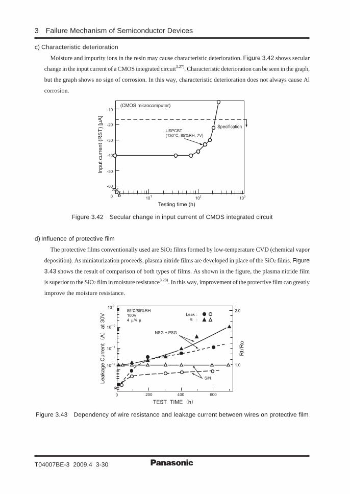
Moisture and impurity ions in the resin may cause characteristic deterioration. Figure 3.42 shows secular
change in the input current of a CMOS integrated circuit3.27). Characteristic deterioration can be seen in the graph,
but the graph shows no sign of corrosion. In this way, characteristic deterioration does not always cause Al
corrosion.
(CMOS microcomputer)
USPCBT(130°C, 85%RH, 7V)
Specification
Input curr
en
t (R
ST
) [µ
A]
Testing time (h)
-60
0
-50
-40
-30
-20
-10
101
102
103
Figure 3.42 Secular change in input current of CMOS integrated circuit
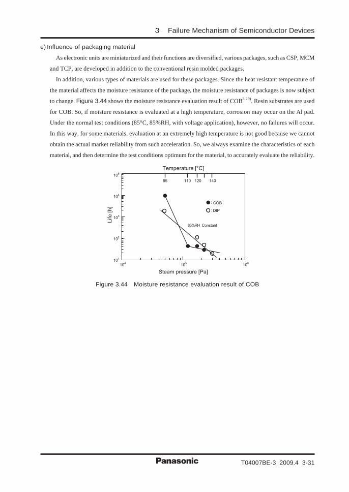
d) Influence of protective film
The protective films conventionally used are SiO2 films formed by low-temperature CVD (chemical vapor
deposition). As miniaturization proceeds, plasma nitride films are developed in place of the SiO2 films. Figure
3.43 shows the result of comparison of both types of films. As shown in the figure, the plasma nitride film
is superior to the SiO2 film in moisture resistance3.28). In this way, improvement of the protective film can greatly
improve the moisture resistance.
NSG + PSG
85 /85%RH100V4 μ/4 μ
SiN
Le
aka
ge
Cu
rre
nt
Aa
t 3
0V
TEST TIME h
0 200 400 600
10-9
10-10
10-11
10-12 1.0
2.0
Rt/
Ro
Leak
R
Figure 3.43 Dependency of wire resistance and leakage current between wires on protective film
Failure Mechanism of Semiconductor Devices
T04007BE-3 2009.4 3-31
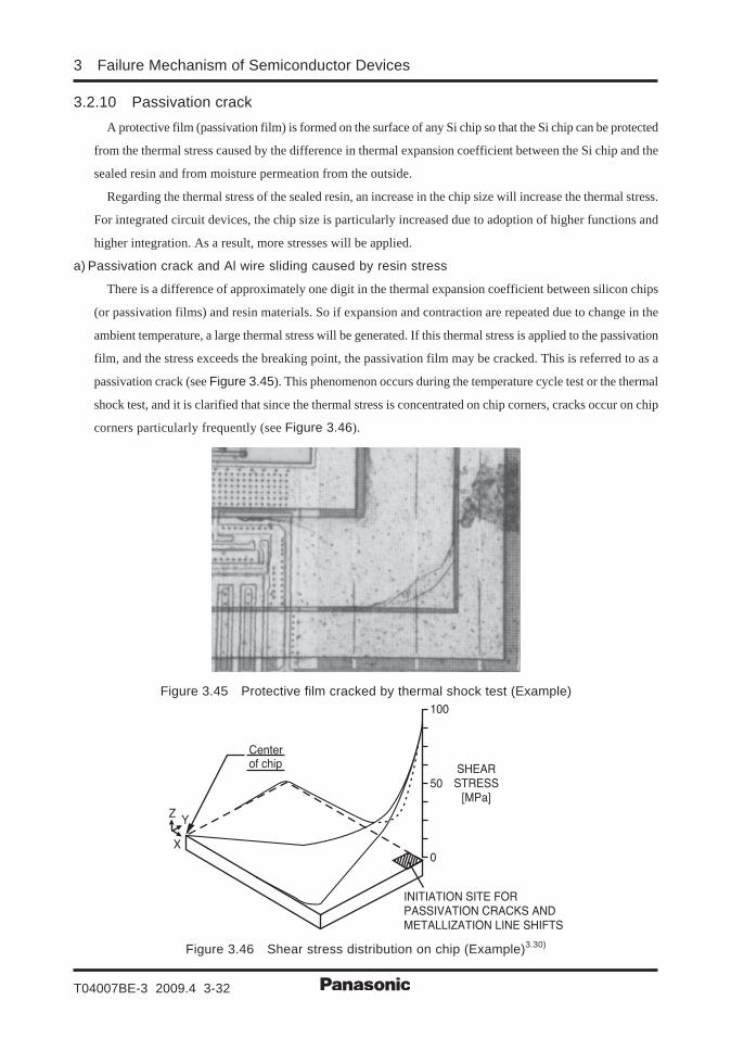
e) Influence of packaging material
As electronic units are miniaturized and their functions are diversified, various packages, such as CSP, MCM
and TCP, are developed in addition to the conventional resin molded packages.
In addition, various types of materials are used for these packages. Since the heat resistant temperature of
the material affects the moisture resistance of the package, the moisture resistance of packages is now subject
to change. Figure 3.44 shows the moisture resistance evaluation result of COB3.29). Resin substrates are used
for COB. So, if moisture resistance is evaluated at a high temperature, corrosion may occur on the Al pad.
Under the normal test conditions (85°C, 85%RH, with voltage application), however, no failures will occur.
In this way, for some materials, evaluation at an extremely high temperature is not good because we cannot
obtain the actual market reliability from such acceleration. So, we always examine the characteristics of each
material, and then determine the test conditions optimum for the material, to accurately evaluate the reliability.
105
104
104
105
106
103
102
101
85 110 120 140
: COB
: DIP
85%RH Constant
Temperature [°C]
Steam pressure [Pa]
Life
[h
]
Figure 3.44 Moisture resistance evaluation result of COB
3 Failure Mechanism of Semiconductor Devices
T04007BE-3 2009.4 3-32
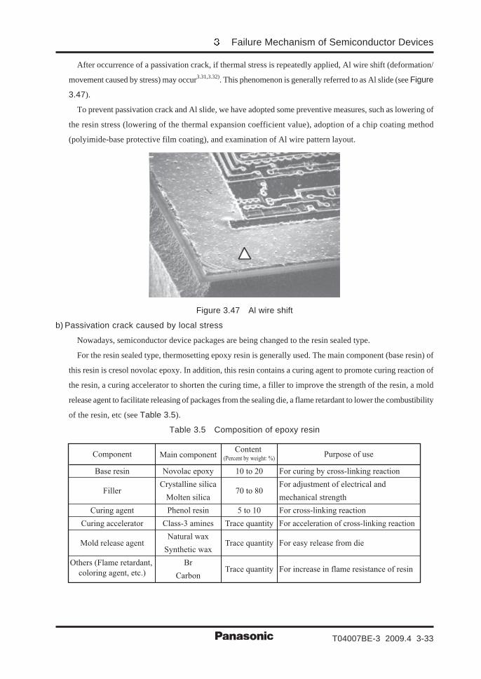
3.2.10 Passivation crackA protective film (passivation film) is formed on the surface of any Si chip so that the Si chip can be protected
from the thermal stress caused by the difference in thermal expansion coefficient between the Si chip and the
sealed resin and from moisture permeation from the outside.
Regarding the thermal stress of the sealed resin, an increase in the chip size will increase the thermal stress.
For integrated circuit devices, the chip size is particularly increased due to adoption of higher functions and
higher integration. As a result, more stresses will be applied.
a) Passivation crack and Al wire sliding caused by resin stress
There is a difference of approximately one digit in the thermal expansion coefficient between silicon chips
(or passivation films) and resin materials. So if expansion and contraction are repeated due to change in the
ambient temperature, a large thermal stress will be generated. If this thermal stress is applied to the passivation
film, and the stress exceeds the breaking point, the passivation film may be cracked. This is referred to as a
passivation crack (see Figure 3.45). This phenomenon occurs during the temperature cycle test or the thermal
shock test, and it is clarified that since the thermal stress is concentrated on chip corners, cracks occur on chip
corners particularly frequently (see Figure 3.46).
Figure 3.45 Protective film cracked by thermal shock test (Example)
Figure 3.46 Shear stress distribution on chip (Example)3.30)
Failure Mechanism of Semiconductor Devices
T04007BE-3 2009.4 3-33
After occurrence of a passivation crack, if thermal stress is repeatedly applied, Al wire shift (deformation/
movement caused by stress) may occur3.31,3.32). This phenomenon is generally referred to as Al slide (see Figure
3.47).
To prevent passivation crack and Al slide, we have adopted some preventive measures, such as lowering of
the resin stress (lowering of the thermal expansion coefficient value), adoption of a chip coating method
(polyimide-base protective film coating), and examination of Al wire pattern layout.
Figure 3.47 Al wire shift
b) Passivation crack caused by local stress
Nowadays, semiconductor device packages are being changed to the resin sealed type.
For the resin sealed type, thermosetting epoxy resin is generally used. The main component (base resin) of
this resin is cresol novolac epoxy. In addition, this resin contains a curing agent to promote curing reaction of
the resin, a curing accelerator to shorten the curing time, a filler to improve the strength of the resin, a mold
release agent to facilitate releasing of packages from the sealing die, a flame retardant to lower the combustibility
of the resin, etc (see Table 3.5).
Table 3.5 Composition of epoxy resin
Component Main component Purpose of useContent
(Percent by weight: %)
Base resin
Filler
Curing agent
Curing accelerator
Mold release agent
Others (Flame retardant,
coloring agent, etc.)
Novolac epoxy
Crystalline silica
Molten silica
Phenol resin
Class-3 amines
Natural wax
Synthetic wax
Br
Carbon
10 to 20
70 to 80
5 to 10
Trace quantity
Trace quantity
Trace quantity
For curing by cross-linking reaction
For adjustment of electrical and
mechanical strength
For cross-linking reaction
For acceleration of cross-linking reaction
For easy release from die
For increase in flame resistance of resin
3 Failure Mechanism of Semiconductor Devices
T04007BE-3 2009.4 3-34
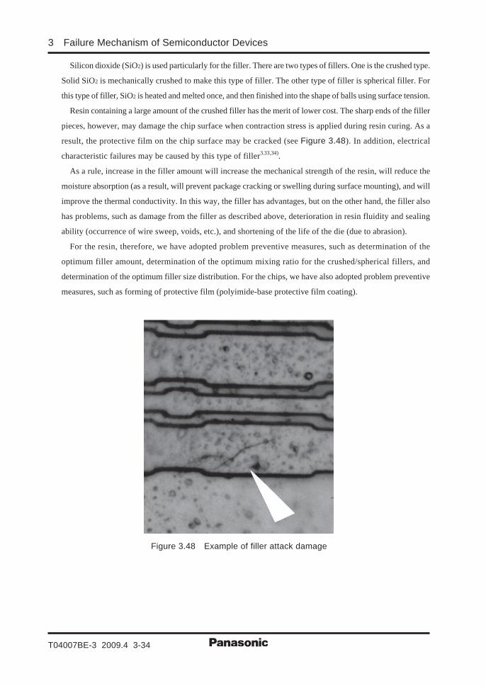
Silicon dioxide (SiO2) is used particularly for the filler. There are two types of fillers. One is the crushed type.
Solid SiO2 is mechanically crushed to make this type of filler. The other type of filler is spherical filler. For
this type of filler, SiO2 is heated and melted once, and then finished into the shape of balls using surface tension.
Resin containing a large amount of the crushed filler has the merit of lower cost. The sharp ends of the filler
pieces, however, may damage the chip surface when contraction stress is applied during resin curing. As a
result, the protective film on the chip surface may be cracked (see Figure 3.48). In addition, electrical
characteristic failures may be caused by this type of filler3.33,34).
As a rule, increase in the filler amount will increase the mechanical strength of the resin, will reduce the
moisture absorption (as a result, will prevent package cracking or swelling during surface mounting), and will
improve the thermal conductivity. In this way, the filler has advantages, but on the other hand, the filler also
has problems, such as damage from the filler as described above, deterioration in resin fluidity and sealing
ability (occurrence of wire sweep, voids, etc.), and shortening of the life of the die (due to abrasion).
For the resin, therefore, we have adopted problem preventive measures, such as determination of the
optimum filler amount, determination of the optimum mixing ratio for the crushed/spherical fillers, and
determination of the optimum filler size distribution. For the chips, we have also adopted problem preventive
measures, such as forming of protective film (polyimide-base protective film coating).
Figure 3.48 Example of filler attack damage
Failure Mechanism of Semiconductor Devices
T04007BE-3 2009.4 3-35
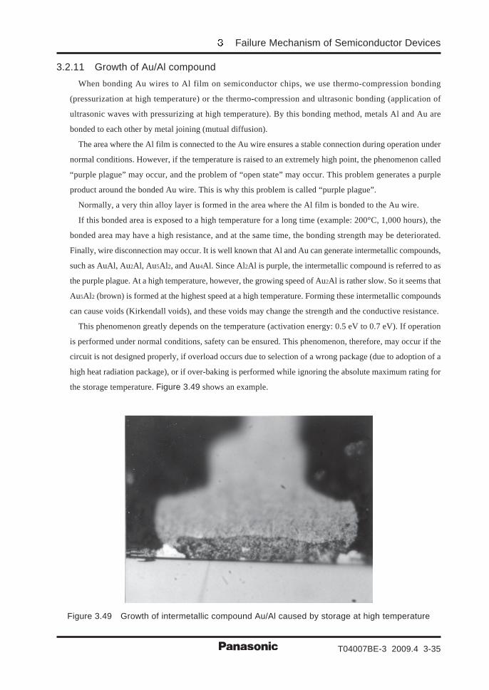
3.2.11 Growth of Au/Al compoundWhen bonding Au wires to Al film on semiconductor chips, we use thermo-compression bonding
(pressurization at high temperature) or the thermo-compression and ultrasonic bonding (application of
ultrasonic waves with pressurizing at high temperature). By this bonding method, metals Al and Au are
bonded to each other by metal joining (mutual diffusion).
The area where the Al film is connected to the Au wire ensures a stable connection during operation under
normal conditions. However, if the temperature is raised to an extremely high point, the phenomenon called
“purple plague” may occur, and the problem of “open state” may occur. This problem generates a purple
product around the bonded Au wire. This is why this problem is called “purple plague”.
Normally, a very thin alloy layer is formed in the area where the Al film is bonded to the Au wire.
If this bonded area is exposed to a high temperature for a long time (example: 200°C, 1,000 hours), the
bonded area may have a high resistance, and at the same time, the bonding strength may be deteriorated.
Finally, wire disconnection may occur. It is well known that Al and Au can generate intermetallic compounds,
such as AuAl, Au2Al, Au5Al2, and Au4Al. Since Al2Al is purple, the intermetallic compound is referred to as
the purple plague. At a high temperature, however, the growing speed of Au2Al is rather slow. So it seems that
Au5Al2 (brown) is formed at the highest speed at a high temperature. Forming these intermetallic compounds
can cause voids (Kirkendall voids), and these voids may change the strength and the conductive resistance.
This phenomenon greatly depends on the temperature (activation energy: 0.5 eV to 0.7 eV). If operation
is performed under normal conditions, safety can be ensured. This phenomenon, therefore, may occur if the
circuit is not designed properly, if overload occurs due to selection of a wrong package (due to adoption of a
high heat radiation package), or if over-baking is performed while ignoring the absolute maximum rating for
the storage temperature. Figure 3.49 shows an example.
Figure 3.49 Growth of intermetallic compound Au/Al caused by storage at high temperature
3 Failure Mechanism of Semiconductor Devices
T04007BE-3 2009.4 3-36
3.2.12 Secondary breakdownThe reverse voltage at the p-n junction of a diode or a transistor is restricted by the avalanche breakdown
voltage generated in the depletion layer. If the voltage applied from the outside is higher than these voltage
values, the insulation of the p-n junction will be broken, and the reverse current will be rapidly increased. This
type of breakdown is referred to as an avalanche breakdown or the primary breakdown.
If the voltage applied from the outside is increased, or if the external resistance is reduced, the reverse
current will be further increased. However, if the reverse current is increased to a certain point, the reverse
voltage will rapidly drop to a low voltage Vs as shown in Figure 3.50. In this status, the current is centered
at a certain part of the electrode. So if this status is kept for a comparatively long time, the current will melt
and penetrate the part to make a small hole. As a result, the device will not function as a diode or a transistor.
This type of phenomenon is referred to as the secondary breakdown so that it can be distinguished from the
primary breakdown.
The secondary breakdown generally occurs when a comparatively high power is applied to a diode or a
transistor. From the viewpoint of current-voltage characteristics, the reverse voltage will rapidly drop after
the voltage rises to VM. Figure 3.50 shows the current-voltage (IC-VCE) characteristic curves that illustrate
the secondary breakdown of transistors. For curves O, R, and F, the bias condition between the emitter and
the base is respectively set to open base terminal, reverse bias, and forward bias. For the secondary breakdown,
the electric power application time is the most important. This means that even if the applied power is high,
application for a short time cannot cause the secondary breakdown. On the contrary, even if the applied
power is low, application for a long time may cause the secondary breakdown. The power application time
required for occurrence of the secondary breakdown is referred to as the delay time Td for the secondary
breakdown. For a given application power, if a device has a long delay time (has a large Td value), the device
will be durable and will not easily cause the secondary breakdown. If the application power is increased, the
delay time Td will be shortened. On the contrary, if the application power is lowered, the delay time Td will
be prolonged. The minimum power that can reduce the Td value to infinity is the maximum power that can
be stably applied during DC operation. The area that can ensure such power and Td is referred to as the
transistor ASO (area of safe operation). The transistor ASO is specified for each model. So the specified ASO
should be regarded as the restriction that is equivalent to the absolute maximum rating. If the specified ASO
is observed in practical use, no problem will occur.
Failure Mechanism of Semiconductor Devices
T04007BE-3 2009.4 3-37
VS
IC
F
R
VCE
VM
O
Figure 3.50 IC-VCE characteristic of secondary breakdown
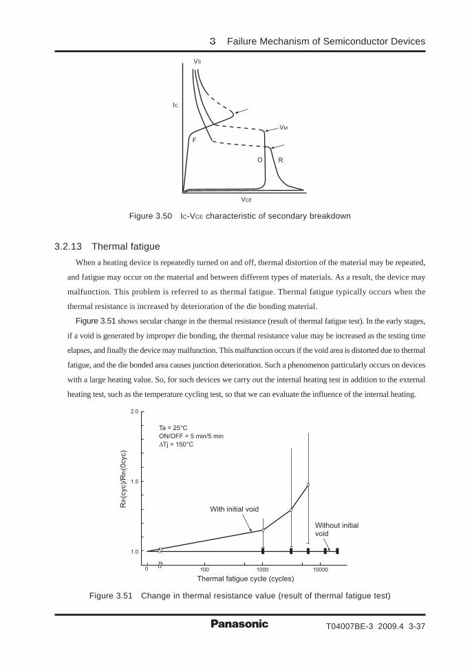
3.2.13 Thermal fatigueWhen a heating device is repeatedly turned on and off, thermal distortion of the material may be repeated,
and fatigue may occur on the material and between different types of materials. As a result, the device may
malfunction. This problem is referred to as thermal fatigue. Thermal fatigue typically occurs when the
thermal resistance is increased by deterioration of the die bonding material.
Figure 3.51 shows secular change in the thermal resistance (result of thermal fatigue test). In the early stages,
if a void is generated by improper die bonding, the thermal resistance value may be increased as the testing time
elapses, and finally the device may malfunction. This malfunction occurs if the void area is distorted due to thermal
fatigue, and the die bonded area causes junction deterioration. Such a phenomenon particularly occurs on devices
with a large heating value. So, for such devices we carry out the internal heating test in addition to the external
heating test, such as the temperature cycling test, so that we can evaluate the influence of the internal heating.
2.0
1.5
1.0
0 100 1000 10000
Without initial void
Thermal fatigue cycle (cycles)
Rth
(cyc)/
Rth
(0cyc)
Ta = 25°C
ON/OFF = 5 min/5 min
ΔTj = 150°C
With initial void
Figure 3.51 Change in thermal resistance value (result of thermal fatigue test)
3 Failure Mechanism of Semiconductor Devices
T04007BE-3 2009.4 3-38
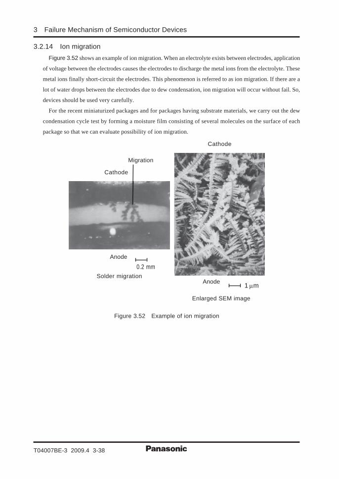
3.2.14 Ion migrationFigure 3.52 shows an example of ion migration. When an electrolyte exists between electrodes, application
of voltage between the electrodes causes the electrodes to discharge the metal ions from the electrolyte. These
metal ions finally short-circuit the electrodes. This phenomenon is referred to as ion migration. If there are a
lot of water drops between the electrodes due to dew condensation, ion migration will occur without fail. So,
devices should be used very carefully.
For the recent miniaturized packages and for packages having substrate materials, we carry out the dew
condensation cycle test by forming a moisture film consisting of several molecules on the surface of each
package so that we can evaluate possibility of ion migration.
Figure 3.52 Example of ion migration
Enlarged SEM image
Cathode
Anode
Anode
Cathode
Migration
0.2 mm Solder migration
1 μm
Failure Mechanism of Semiconductor Devices
T04007BE-3 2009.4 3-39
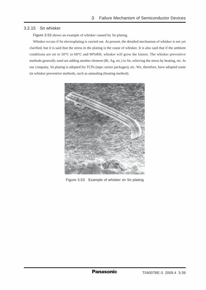
3.2.15 Sn whiskerFigure 3.53 shows an example of whisker caused by Sn plating.
Whisker occurs if Sn electroplating is carried out. At present, the detailed mechanism of whisker is not yet
clarified, but it is said that the stress in the plating is the cause of whisker. It is also said that if the ambient
conditions are set to 50°C to 60°C and 90%RH, whisker will grow the fastest. The whisker preventive
methods generally used are adding another element (Bi, Ag, etc.) to Sn, relieving the stress by heating, etc. In
our company, Sn plating is adopted for TCPs (tape carrier packages), etc. We, therefore, have adopted some
tin whisker preventive methods, such as annealing (heating method).
Figure 3.53 Example of whisker on Sn plating
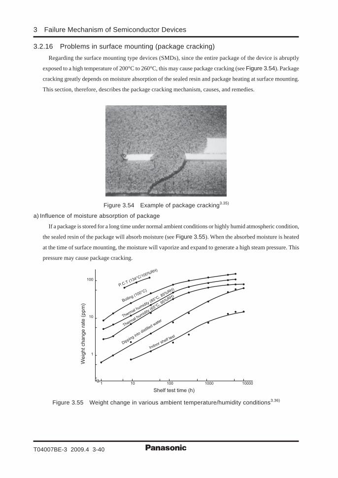
3 Failure Mechanism of Semiconductor Devices
T04007BE-3 2009.4 3-40
3.2.16 Problems in surface mounting (package cracking)Regarding the surface mounting type devices (SMDs), since the entire package of the device is abruptly
exposed to a high temperature of 200°C to 260°C, this may cause package cracking (see Figure 3.54). Package
cracking greatly depends on moisture absorption of the sealed resin and package heating at surface mounting.
This section, therefore, describes the package cracking mechanism, causes, and remedies.
Figure 3.54 Example of package cracking3.35)
a) Influence of moisture absorption of package
If a package is stored for a long time under normal ambient conditions or highly humid atmospheric condition,
the sealed resin of the package will absorb moisture (see Figure 3.55). When the absorbed moisture is heated
at the time of surface mounting, the moisture will vaporize and expand to generate a high steam pressure. This
pressure may cause package cracking.
Shelf test time (h)
We
igh
t ch
an
ge
ra
te (
pp
m)
P.C.T (134°C/100%RH)
Thermal h
umidity (8
5°C, 8
5%RH)
Thermal h
umidity (6
5°C, 9
5%RH)Boilin
g (100°C)
Dipping into distill
ed water
Indoor shelf te
st
1 10 100 1000 10000
1
10
100
Figure 3.55 Weight change in various ambient temperature/humidity conditions3.36)
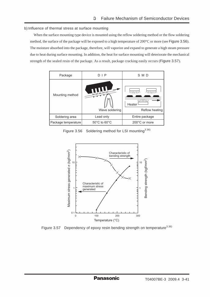
Failure Mechanism of Semiconductor Devices
T04007BE-3 2009.4 3-41
b) Influence of thermal stress at surface mounting
When the surface mounting type device is mounted using the reflow soldering method or the flow soldering
method, the surface of the package will be exposed to a high temperature of 200°C or more (see Figure 3.56).
The moisture absorbed into the package, therefore, will vaporize and expand to generate a high steam pressure
due to heat during surface mounting. In addition, the heat for surface mounting will deteriorate the mechanical
strength of the sealed resin of the package. As a result, package cracking easily occurs (Figure 3.57).
Package
Wave soldering Reflow heating
D I P S M D
Lead only Entire package
50°C to 60°C 200°C or more
Mounting method
Soldering area
Package temperature
Heater
Figure 3.56 Soldering method for LSI mounting3.36)
0
0.1
1
10
100 200 300
Temperature (°C)
Maxim
um
str
ess g
enera
ted σ
(kgf/m
m2)
1
10
Bendin
g s
trength
(kgf/m
m2)
Characteristic of bending strength
Characteristic of maximum stress generated
Figure 3.57 Dependency of epoxy resin bending strength on temperature3.36)
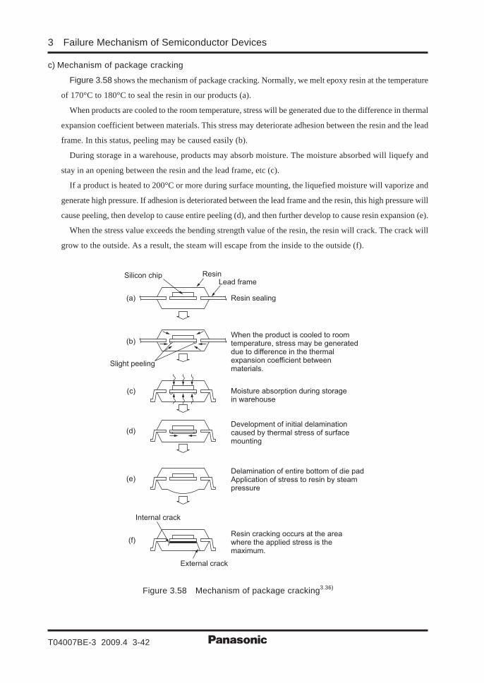
3 Failure Mechanism of Semiconductor Devices
T04007BE-3 2009.4 3-42
c) Mechanism of package cracking
Figure 3.58 shows the mechanism of package cracking. Normally, we melt epoxy resin at the temperature
of 170°C to 180°C to seal the resin in our products (a).
When products are cooled to the room temperature, stress will be generated due to the difference in thermal
expansion coefficient between materials. This stress may deteriorate adhesion between the resin and the lead
frame. In this status, peeling may be caused easily (b).
During storage in a warehouse, products may absorb moisture. The moisture absorbed will liquefy and
stay in an opening between the resin and the lead frame, etc (c).
If a product is heated to 200°C or more during surface mounting, the liquefied moisture will vaporize and
generate high pressure. If adhesion is deteriorated between the lead frame and the resin, this high pressure will
cause peeling, then develop to cause entire peeling (d), and then further develop to cause resin expansion (e).
When the stress value exceeds the bending strength value of the resin, the resin will crack. The crack will
grow to the outside. As a result, the steam will escape from the inside to the outside (f).
(a)
(b)
(c)
(d)
(e)
(f)
Resin sealing
Moisture absorption during storage in warehouse
Development of initial delamination caused by thermal stress of surface mounting
Silicon chip ResinLead frame
Slight peeling
Internal crack
External crack
Delamination of entire bottom of die padApplication of stress to resin by steam pressure
When the product is cooled to room temperature, stress may be generated due to difference in the thermal expansion coefficient between materials.
Resin cracking occurs at the area where the applied stress is the maximum.
Figure 3.58 Mechanism of package cracking3.36)
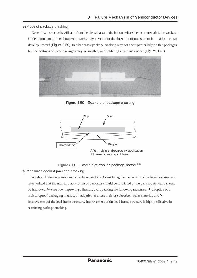
Failure Mechanism of Semiconductor Devices
T04007BE-3 2009.4 3-43
e) Mode of package cracking
Generally, most cracks will start from the die pad area to the bottom where the resin strength is the weakest.
Under some conditions, however, cracks may develop in the direction of one side or both sides, or may
develop upward (Figure 3.59). In other cases, package cracking may not occur particularly on thin packages,
but the bottoms of these packages may be swollen, and soldering errors may occur (Figure 3.60).
Figure 3.59 Example of package cracking
Chip Resin
Die padDelamination
(After moisture absorption + application
of thermal stress by soldering)
Figure 3.60 Example of swollen package bottom3.37)
f) Measures against package cracking
We should take measures against package cracking. Considering the mechanism of package cracking, we
have judged that the moisture absorption of packages should be restricted or the package structure should
be improved. We are now improving adhesion, etc. by taking the following measures: adoption of a
moistureproof packaging method, adoption of a less moisture absorbent resin material, and
improvement of the lead frame structure. Improvement of the lead frame structure is highly effective in
restricting package cracking.
3 Failure Mechanism of Semiconductor Devices
T04007BE-3 2009.4 3-44
3.2.17 Electrostatic discharge (ESD)As semiconductor devices are miniaturized, the resistance to static electricity is being deteriorated. So, this
section describes the failure modes, mechanisms and damage models regarding electrostatic damage of
semiconductor devices, and also describes evaluation method and remedies.
a) Electrostatic discharge models
1) Damage models
A semiconductor device causes electrostatic discharge if external static electricity is discharged to the device,
if static electricity stored in the device is discharged to an external conductor, or if the electric field condition
around the device is abruptly changed. Based on these facts, electrostatic discharge models can be classified
as shown in Table 3.6.
Table 3.6 Electrostatic discharge models
A (Large capacity, comparatively low speed)
B (Small capacity, high speed) C
Description of model: A metal or a conductor near the device is electrostatically charged, and then the charged static electricity is discharged to a terminal of the device. As a result, electrostatic discharge will occur.
Description of model: The device is directly or indirectly charged with static electricity, and a terminal of the device discharges the static electricity to a metal or a conductor near the device. As a result, electrostatic discharge will occur.
Description of model: Transient voltage or overcurrent is generated inside the device due to a change in the electric field around the device. As a result, electrostatic discharge will occur.
Human body model (HBM)Description of model: The body of a human being who is handling the device is electrostatically charged, and then the charged static electricity is discharged to the device.Machine model (MM)Description of model: A metal casing in contact with the device is electrostatically charged, and then the charged static electricity is discharged to the device.
Charged device model (CDM)Description of model: The device metal or conductor is electrostatically charged.Charged package model (CPM)Description of model: The device sealing resin is electrostatically charged in the friction process, etc.Electrostatically charged body induction model (EBIM)Description of model: The device is electrostatically charged by induction of an electrostatically charged insulator or conductor near the device.
Electric field induction model (FIM)
2) Failure modes and mechanisms
When static electricity is applied to a semiconductor device, elements in the device may be damaged. So
leakage current may flow mainly, and the characteristics of the device may deteriorate. If an extremely high static
electricity is applied to a device (though such a problem rarely occurs), the electrostatic energy may melt the
wire material, etc. So an “open” failure may occur.
The mechanisms of device damage and deterioration caused by static electricity can be roughly classified
into two types. One type is the thermal damage type, and the other type is the electric field damage type.
Table 3.7 shows the electrostatic discharge mechanisms of semiconductors. In this table, the term “thermo-
runaway” means that the device is extremely heated by the power supply current so that the device temperature
exceeds the intrinsic temperature peak value shown by the temperature-resistance curve, and also means that
the resistance value is abruptly changed to the negative characteristic value, and the cycle of “current increase
⇒ resistance reduction ⇒ current increase ⇒ resistance reduction” is repeated. Figures 3.61 respectively
show typical examples of damage by electrostatic discharge: junction damage of a MOS transistor, junction
damage of a bipolar transistor, and Al wire melting.
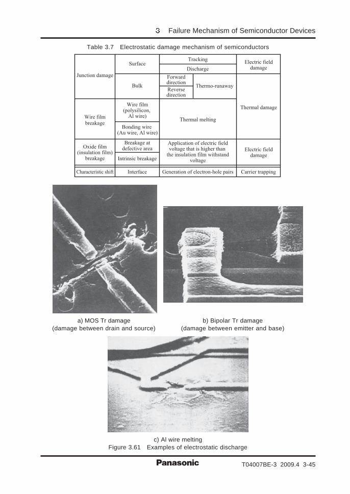
Failure Mechanism of Semiconductor Devices
T04007BE-3 2009.4 3-45
Table 3.7 Electrostatic damage mechanism of semiconductors
Junction damage
Wire film breakage
Oxide film (insulation film)
breakage
Wire film (polysilicon,
Al wire)
Bonding wire (Au wire, Al wire)
Application of electric field voltage that is higher than
the insulation film withstand voltage
Thermal melting
SurfaceTracking
Electric field damage
Electric field damage
Thermal damage
Discharge
Forward direction
Reverse direction
Thermo-runawayBulk
Breakage at defective area
Intrinsic breakage
Interface Carrier trappingGeneration of electron-hole pairsCharacteristic shift
a) MOS Tr damage b) Bipolar Tr damage(damage between drain and source) (damage between emitter and base)
c) Al wire meltingFigure 3.61 Examples of electrostatic discharge
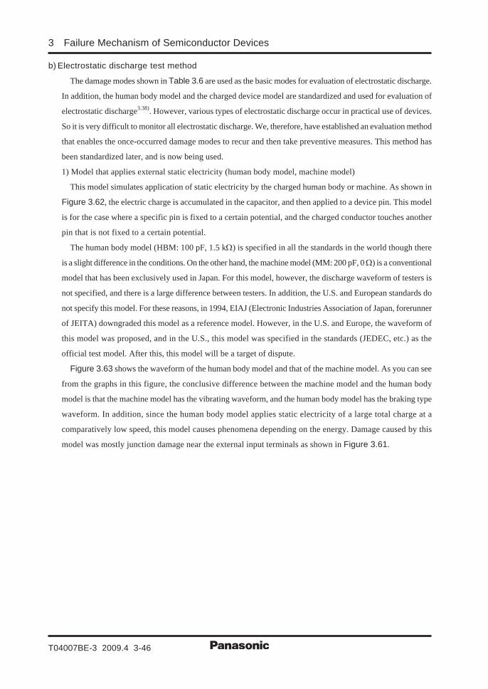
3 Failure Mechanism of Semiconductor Devices
T04007BE-3 2009.4 3-46
b) Electrostatic discharge test method
The damage modes shown in Table 3.6 are used as the basic modes for evaluation of electrostatic discharge.
In addition, the human body model and the charged device model are standardized and used for evaluation of
electrostatic discharge3.38). However, various types of electrostatic discharge occur in practical use of devices.
So it is very difficult to monitor all electrostatic discharge. We, therefore, have established an evaluation method
that enables the once-occurred damage modes to recur and then take preventive measures. This method has
been standardized later, and is now being used.
1) Model that applies external static electricity (human body model, machine model)
This model simulates application of static electricity by the charged human body or machine. As shown in
Figure 3.62, the electric charge is accumulated in the capacitor, and then applied to a device pin. This model
is for the case where a specific pin is fixed to a certain potential, and the charged conductor touches another
pin that is not fixed to a certain potential.
The human body model (HBM: 100 pF, 1.5 kΩ) is specified in all the standards in the world though there
is a slight difference in the conditions. On the other hand, the machine model (MM: 200 pF, 0 Ω) is a conventional
model that has been exclusively used in Japan. For this model, however, the discharge waveform of testers is
not specified, and there is a large difference between testers. In addition, the U.S. and European standards do
not specify this model. For these reasons, in 1994, EIAJ (Electronic Industries Association of Japan, forerunner
of JEITA) downgraded this model as a reference model. However, in the U.S. and Europe, the waveform of
this model was proposed, and in the U.S., this model was specified in the standards (JEDEC, etc.) as the
official test model. After this, this model will be a target of dispute.
Figure 3.63 shows the waveform of the human body model and that of the machine model. As you can see
from the graphs in this figure, the conclusive difference between the machine model and the human body
model is that the machine model has the vibrating waveform, and the human body model has the braking type
waveform. In addition, since the human body model applies static electricity of a large total charge at a
comparatively low speed, this model causes phenomena depending on the energy. Damage caused by this
model was mostly junction damage near the external input terminals as shown in Figure 3.61.
Failure Mechanism of Semiconductor Devices
T04007BE-3 2009.4 3-47
Rp Rd
Cd Cd
HBM MM
100 pF 200 pF
1500 Ω 0 ΩRdV
Device UnderTest
Protective resistance(10 MΩ)
Applied voltage
HBH (1000 V):Pulse width (peak value: 36.8%) = 151.6 nsRise time = 8.06 ns
MM (1000 V):Pulse width (half width) = 17.5 nsRise time = 7.8 ns
Figure 3.62 Test circuit Figure 3.63 Waveforms of HBM and MM
2) Model that discharges static electricity from charged device (charged device model, charged package model)
As the semiconductors are miniaturized, we have new problems that are different from the damage problems
of the human body model or the machine model. In addition to the junction damage, gate oxide film breakage
and insulation film breakage occur now. Moreover, damage occurs not only near the external input terminal
but also on the internal circuit3.39). Figure 3.64 shows the example of damage that occurred in the stamp type
marking process. This example shows the breakage of the gate oxide film3.40).
Figure 3.64 Example of electrostatic discharge (breakage of gate oxide film) in marking process
Since the insulation film was broken, we judged that the cause was application of a high voltage. In addition,
since the breakage developed to the internal circuit without passing through the protective circuit of the
external input terminal, we assumed that this breakage had an extremely high-speed pulse waveform. At that
time, however, this phenomenon was unclear, and the waveform measurement method was unknown. So we
examined some methods that could simulate the damage occurrence process. For example, these methods are
the rotary shaker method3.41), shaking method3.42), and “stirring on metal plate” method. In our company, the
rotary shaker method has been used for in-house evaluation for several decades. This method, however, uses
friction of vinyl chloride pieces to cause an electric charge. So, there is possibility that the result of the test
3 Failure Mechanism of Semiconductor Devices
T04007BE-3 2009.4 3-48
may be affected by the ambient conditions (particularly by humidity). The shaking method puts samples in
a non-conductive plastic magazine, and then shakes the samples. Whichever method is used, it is difficult to
make a quantitative judgment using these methods. We have been using these methods just for recurrence of
phenomena.
As described above, as semiconductors are miniaturized, the gate oxide films and the insulation films of
MOS transistors are getting thinner and thinner. As a result, the dielectric breakdown voltage is being
deteriorated. In this way, the device strength against electrostatic discharge is being deteriorated, and for this
reason, electric field damage occurs easily. In addition, as the semiconductor manufacturing process and the
electronic equipment assembly process are further automated, devices are subject to more friction. Now,
there are many cases in which devices are electrically charged in the production process. If the lead pin of a
charged device touches metal, electric current will flow and the voltage will rise rapidly. As a result, the
voltage will easily cause electric field damage.
Figure 3.65 shows the charged device model (CDM) and the charged package model (CPM) that are damage
models caused by electrostatic discharge of devices3.43,44).
When adopting the model that discharges static electricity from the charged device, we should use a
different device charging/discharging method, but this method is specified in the JEITA standard3.38) and the
JEDED standard3.45). Figure 3.66 shows the test method specified in the JEITA standard. In addition, Figure
3.67 shows the discharge waveform obtained by the CDM test. Compared with the human body model and
the machine model (see Figure 3.63), this model (CDM) shows a very high-speed pulse3.46).
Charged device model
Tweezers
Grounded metal
Charged package model
Charged device
Discharge
Discharge
Conduction current
Metal plate, etc.
Insulation sheet
Terminal to be tested
Electrode
Test piece
Resistor R3
Metal plate
The switch should be turned on to start discharge.
R1
R2
High-voltage power
Figure 3.65 Model that discharges static Figure 3.66 Example of charged device
electricity from charged device model (CDM) test method
Failure Mechanism of Semiconductor Devices
T04007BE-3 2009.4 3-49
Width = 0.27ns
Rise Time = 0.12ns
Max Value = 3.60V
Fall Time = 0.15ns
Top Level = 3.60V
Figure 3.67 Waveform of CDM test
c) Measures against electrostatic discharge
1) Protective circuit incorporated in semiconductor
To protect semiconductor integrated circuits from static electricity, electrostatic discharge protective devices
or circuits are mounted around semiconductor chips though these protective devices or circuits are not
necessary for assurance of the circuit characteristics. Since static electricity is applied from the lead via the
wire, a protective circuit around the pad will discharge the static electricity to protect internal circuits.
Protective circuits are mounted so that the protective circuit can discharge the applied static electricity to
the GND in the chip or to the power supply line so that the internal circuit can be protected from static electricity.
By the way, if static electricity is applied, the protective circuit may be damaged, or the leakage current may
flow to cause abnormal operation of the semiconductor integrated circuit. So the protective circuit should
discharge static electricity as quickly as possible (so that static electricity cannot reach the internal circuit).
In addition, the protective circuit should be highly resistant to static electricity. Further, for the operation, it
should have a structure not to cause leakage current.
2) Basic design of protective circuit
A protective circuit uses a bypass circuit of a low impedance to restrict the discharge voltage or the discharge
current so that the discharge voltage or current value can be below the dielectric strength value of the internal
device. For this reason, we should construct a protective circuit that can protect this bypass circuit from
damage, and can absorb almost all the static charge. The following devices are used for restriction of current
and voltage:
(a) Current limiter device: Diffusion resistor, polysilicon resistor
(b)Voltage limiter device: P-N junction diode, MOS transistor, and diode
Figure 3.68 and Figure 3.69 respectively show the basic devices of electrostatic discharge protective
circuits and the protective circuits generally used. For protective devices, the electrostatic discharge resistance
depends on the device size. For this reason, we optimize the size of each protective device to ensure the target
resistance. However, if the size is extremely enlarged, the cost will be too high. Adoption of such a large size
is not economical. Figure 3.70 and Figure 3.71 respectively show the size dependency of the P-N junction
diode and the MOS transistor diode3.46,47).
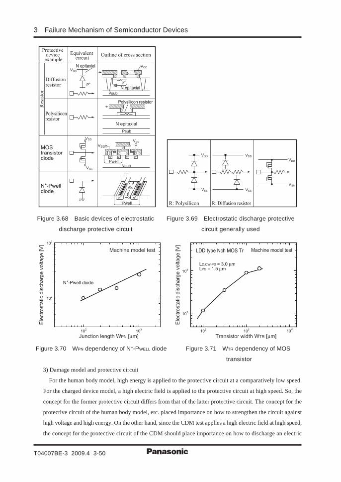
3 Failure Mechanism of Semiconductor Devices
T04007BE-3 2009.4 3-50
Protective device
example
Equivalent circuit
Outline of cross section
Diffusion resistor
Polysilicon resistor
MOS transistor diode
N+-Pwell diode
VCC
VCC
VDD
VSS
VDD
VSS
P+ P
+
Psub
Psub
NsubPwell
Pwell
N epitaxial
N epitaxial
Polysilicon resistor
N epitaxial
N+
N+
P+
P+
N+
P+
WPN
R: Polysilicon R: Diffusion resistor
VDD
VSS
VDD
VSS
VDD
VSS
Res
isto
r
Figure 3.68 Basic devices of electrostatic Figure 3.69 Electrostatic discharge protective
discharge protective circuit circuit generally used
102
103
102
N+-Pwell diode
LDD type Nch MOS Tr
LD.CW-PS = 3.0 μmLPS = 1.5 μm
Machine model test Machine model test
103
Ele
ctr
osta
tic d
ischarg
e v
oltage [V
]
Junction length WPN [μm]
102
103
104
102
103
Ele
ctr
osta
tic d
ischarg
e v
oltage [V
]
Transistor width WTR [μm]
Figure 3.70 WPN dependency of N+-PWELL diode Figure 3.71 WTR dependency of MOS
transistor
3) Damage model and protective circuit
For the human body model, high energy is applied to the protective circuit at a comparatively low speed.
For the charged device model, a high electric field is applied to the protective circuit at high speed. So, the
concept for the former protective circuit differs from that of the latter protective circuit. The concept for the
protective circuit of the human body model, etc. placed importance on how to strengthen the circuit against
high voltage and high energy. On the other hand, since the CDM test applies a high electric field at high speed,
the concept for the protective circuit of the CDM should place importance on how to discharge an electric
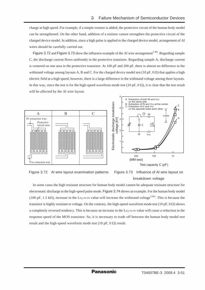
Failure Mechanism of Semiconductor Devices
T04007BE-3 2009.4 3-51
charge at high speed. For example, if a simple resistor is added, the protective circuit of the human body model
can be strengthened. On the other hand, addition of a resistor cannot strengthen the protective circuit of the
charged device model. In addition, since a high pulse is applied to the charged device model, arrangement of Al
wires should be carefully carried out.
Figure 3.72 and Figure 3.73 show the influence example of the Al wire arrangement3.48). Regarding sample
C, the discharge current flows uniformly in the protective transistor. Regarding sample A, discharge current
is centered on one area in the protective transistor. At 100 pF and 200 pF, there is almost no difference in the
withstand voltage among layouts A, B and C. For the charged device model test (10 pF, 0 Ω) that applies a high
electric field at a high speed, however, there is a large difference in the withstand voltage among three layouts.
In this way, since the test is for the high-speed waveform mode test (10 pF, 0 Ω), it is clear that the test result
will be affected by the Al wire layout.
A
IN extraction wire
VDD extraction wire
B C
Protective circuit area
5
4
3
2
1
200 100 10
C
B
A
C
VDD
IN1100V
(MM test)
Test capacity C (pF)
Ele
ctr
osta
tic d
ischarg
e b
reakdow
n
voltage [
kV
]
A: Extraction of both IN and VDD on the same sideB: Extraction of IN and VDD at the centerC: Extraction of In and VDD on the opposite sides each other
Figure 3.72 Al wire layout examination patterns Figure 3.73 Influence of Al wire layout on
breakdown voltage
In some cases the high resistant structure for human body model cannot be adequate resistant structure for
electrostatic discharge in the high-speed pulse mode. Figure 3.74 shows an example. For the human body model
(100 pF, 1.5 kΩ), increase in the LD,CW-PS value will increase the withstand voltage3.46). This is because the
transistor is highly resistant to voltage. On the contrary, the high-speed waveform mode test (10 pF, 0 Ω) shows
a completely reversed tendency. This is because an increase in the LD,CW-PS value will cause a reduction in the
response speed of the MOS transistor. So, it is necessary to trade off between the human body model test
result and the high-speed waveform mode test (10 pF, 0 Ω) result.
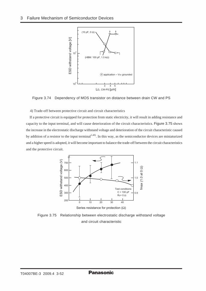
3 Failure Mechanism of Semiconductor Devices
T04007BE-3 2009.4 3-52
102
103
3 4 5
LD, CW-PS [μm]
ES
D w
ith
sta
nd
vo
lta
ge
[V
]
(HBM: 100 pF, 1.5 kΩ)
(10 pF, 0 Ω)
application -- VSS grounded
Figure 3.74 Dependency of MOS transistor on distance between drain CW and PS
4) Trade-off between protective circuit and circuit characteristics
If a protective circuit is equipped for protection from static electricity, it will result in adding resistance and
capacity to the input terminal, and will cause deterioration of the circuit characteristics. Figure 3.75 shows
the increase in the electrostatic discharge withstand voltage and deterioration of the circuit characteristic caused
by addition of a resistor to the input terminal3.49). In this way, as the semiconductor devices are miniaturized
and a higher speed is adopted, it will become important to balance the trade-off between the circuit characteristics
and the protective circuit.
0
300
200
400
500
600
700
10 20 30 40
0.9
1.0
1.1
ES
D w
ithsta
nd v
oltage (
V)
fmax (
1.0
at 0 Ω
)
Series resistance for protection (Ω)
Test conditions:
C = 100 pF
RS= 0 Ω
Figure 3.75 Relationship between electrostatic discharge withstand voltage
and circuit characteristic
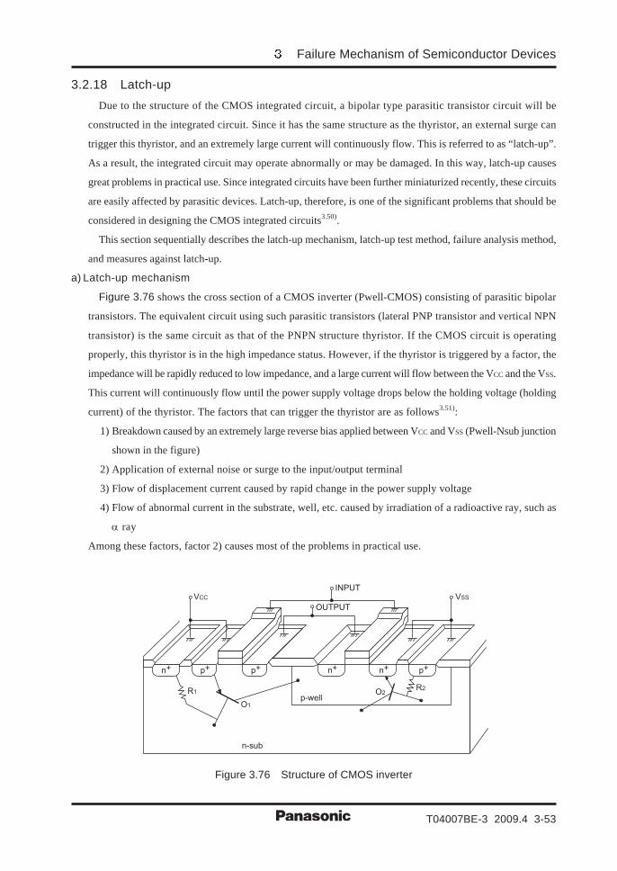
Failure Mechanism of Semiconductor Devices
T04007BE-3 2009.4 3-53
3.2.18 Latch-upDue to the structure of the CMOS integrated circuit, a bipolar type parasitic transistor circuit will be
constructed in the integrated circuit. Since it has the same structure as the thyristor, an external surge can
trigger this thyristor, and an extremely large current will continuously flow. This is referred to as “latch-up”.
As a result, the integrated circuit may operate abnormally or may be damaged. In this way, latch-up causes
great problems in practical use. Since integrated circuits have been further miniaturized recently, these circuits
are easily affected by parasitic devices. Latch-up, therefore, is one of the significant problems that should be
considered in designing the CMOS integrated circuits3.50).
This section sequentially describes the latch-up mechanism, latch-up test method, failure analysis method,
and measures against latch-up.
a) Latch-up mechanism
Figure 3.76 shows the cross section of a CMOS inverter (Pwell-CMOS) consisting of parasitic bipolar
transistors. The equivalent circuit using such parasitic transistors (lateral PNP transistor and vertical NPN
transistor) is the same circuit as that of the PNPN structure thyristor. If the CMOS circuit is operating
properly, this thyristor is in the high impedance status. However, if the thyristor is triggered by a factor, the
impedance will be rapidly reduced to low impedance, and a large current will flow between the VCC and the VSS.
This current will continuously flow until the power supply voltage drops below the holding voltage (holding
current) of the thyristor. The factors that can trigger the thyristor are as follows3.51):
1) Breakdown caused by an extremely large reverse bias applied between VCC and VSS (Pwell-Nsub junction
shown in the figure)
2) Application of external noise or surge to the input/output terminal
3) Flow of displacement current caused by rapid change in the power supply voltage
4) Flow of abnormal current in the substrate, well, etc. caused by irradiation of a radioactive ray, such as
α ray
Among these factors, factor 2) causes most of the problems in practical use.
VCC
INPUTVSS
n+ n+ n+p+
R1R2
O1
O2
p+
p-well
n-sub
p+
OUTPUT
Figure 3.76 Structure of CMOS inverter
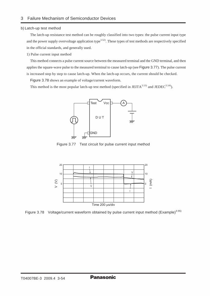
3 Failure Mechanism of Semiconductor Devices
T04007BE-3 2009.4 3-54
b) Latch-up test method
The latch-up resistance test method can be roughly classified into two types: the pulse current input type
and the power supply overvoltage application type3.52). These types of test methods are respectively specified
in the official standards, and generally used.
1) Pulse current input method
This method connects a pulse current source between the measured terminal and the GND terminal, and then
applies the square-wave pulse to the measured terminal to cause latch-up (see Figure 3.77). The pulse current
is increased step by step to cause latch-up. When the latch-up occurs, the current should be checked.
Figure 3.78 shows an example of voltage/current waveform.
This method is the most popular latch-up test method (specified in JEITA3.53) and JEDEC3.54)).
VccTest
D U T
GND
A
Figure 3.77 Test circuit for pulse current input method
20
10
0
20
10
0
Time 200 μs/div
V (V
)
I (
mA
)
I
V
I
V
Figure 3.78 Voltage/current waveform obtained by pulse current input method (Example)3.55)

Failure Mechanism of Semiconductor Devices
T04007BE-3 2009.4 3-55
2) Power supply overvoltage application method
This method is mainly used for evaluation of the latch-up resistance of the VCC terminal. This method increases
the power supply voltage of the device, and checks the change in the power supply current to evaluate the
latch-up resistance (see Figure 3.79).
Vcc
Vcc
GND
A
Overvoltage
Figure 3.79 Test circuit for power supply overvoltage application method
c) Measures against latch-up3.51)
Basically, the measures against latch-up are to deteriorate the parasitic transistor driving performance, to
reduce the resistance of the well and the substrate, and to cut off the thyristor loop. The measures for the
layout design and the process are described below. At present, the measures for the layout are mainly
adopted. However, it seems that further miniaturization will be promoted after this. For this reason, it will be
also important to adopt the measures for the process.
1) Measures for layout design (Examples)
Separation of the LSI into two circuits: the internal circuit and the buffer circuit
Widening the distance between the Pch MOS and Nch MOS in the buffer area
Enclosing of the Pch MOS and the Nch MOS in the buffer area using guard ring for the purpose of
reduction in the well resistance and the substrate resistance and cut-off of the thyristor loop
Reduction in fluctuation of the power supply potential and the GND potential by adopting more N+
contacts in the Nwell area and more P+ contacts in the Pwell area
2) Measures for process (Examples)
Use of high-density epitaxial wafers to reduce the substrate resistance
Assurance of high-density at the wafer bottom only for reducing the well resistance (reduction in the
well resistance without affecting the electric characteristic of the LSI)
Separation of Pch MOS from the Nch MOS by trench oxide
3 Failure Mechanism of Semiconductor Devices
T04007BE-3 2009.4 3-56
Reference documents:
3.1) B.E. Deal, “Standardized Terminology for Oxide Charges Associated with Thermally Oxidized Silicon”,
J. Electrochem. Soc. 127, pp. 979-981 (1980).
3.2) Hara et al., “MOS transistor operation theory”, Kindai Kagaku sha Co., Ltd., p. 13.
3.3) Tokuyama and Hashimoto, “VLSI manufacturing technology”, Nikkei Business Publications, Inc., pp.
22-47.
3.4) Takeda, “Hot carrier effect”, Nikkei McGraw-Hill, Inc. (1987).
3.5) Ajiki, “Reliability Engineering for Semiconductor Devices”, Unions of Japanese Scientists and Engineers,
pp. 163-168.
3.6) Masuoka et al., “A New EEPROM Cell Using Triple Polysilicon Technology”, Proc. IEEE Int., Electron
Device Meet, p. 464 (1984).
3.7) Kume, “Flash memory technology”, OYO BUTURI Vol. 65, No. 11, p. 1114 (1996).
3.8) “Reliability of latest flash memory technology”, Reliability Center for Electronic Components of Japan,
Result Report 1997 issued by Failure Physics Research Committee (R-9-RS-01) (1996).
3.9) A. Brand et al., “Novel Read Disturb Failure Mechanism Induced by Flash Cycling”, Proc. IEEE Int.,
Reliability Physics Symposium, p. 127 (1995).
3.10) J. R. Black, “Mass transport of Al by momentum Exchange with conducting electrons”, Proc. 6th
International Reliability Physics Symposium, pp. 148-159 (1966).
3.11) F. M. d’Heurle et al., “Electromigration in thin Film”, Interdiffusion and Reactions (John Wily & Sons),
pp. 243-303 (1978).
3.12) Wada,“Measures against electro-migration”, Semiconductor World, July (1985), pp. 108-115.
3.13) S. Vaidya et al.,“Effect of texture and grain structures on electromigration in Al-0.5%Cu thin films”, Thin
Solid Films, 75, pp. 253-259 (1981).
3.14) Wada,“Reliability of Al wire”, Semiconductor World, March (1986), pp. 76-83.
3.15) T. Wada,“Barrier Metal Effect on Electro- and Stress-Migration”, IEICE Trans. Fundamentals Vol. E77-
A, No. 1, January 1994, pp. 180-186.
3.16) N. Owada et al.,“Stress induced slit-link void formation in a finepattern Al-Si interconnect during aging
test”, IEEE 2nd International VLSI Multilevel Interconnection Conference, pp. 173-179 (1985).
3.17) S. Mayumi et al.,“The effect of Cu addition to Al-Si interconnects on stress induced open-circuit
failures”, 25th Ann. Proc. International Reliability Physics Symp., pp. 15-21 (1987).
3.18) T. Turner and K. Wendel,“The influence of stress on aluminum conductor life”, 23rd Ann. Proc.
International Reliability Physics Symp., pp. 142-147 (1985).
3.19) Wada et al.,“Electro-migration and stress migration of Al wire”, Research Report of Technical Group of
Reliability, Institute of Electronics, Information and Communication Engineers, R87-36, pp. 19-24
(1987).
3.20) J. Klema et al.,“Reliability implications of nitrogen contamination during deposition of sputtered
aluminum/silicon metal films”, 22nd Ann. Proc. International Reliability Physics Symp., pp. 1-5 (1984).
3.21) “2.1 Cu metallization technology” by Reliability Center for Electronic Components of Japan, Result
Failure Mechanism of Semiconductor Devices
T04007BE-3 2009.4 3-57
Report 2000 issued by Failure Physics Research Committee (R-12-RS-01) pp. 173-174 (2001).
3.22) Hayashi et al., “Electro-migration of Cu wire” , The Journal of Reliability Engineering Association of
Japan, Vol. 25, pp. 110-119 (2003).
3.23) M. Hayashi, “Dependence of Copper Interconnect Electromigration Phenomenon on Barrier Metal
Materials”, 14th ESREF, pp. 1545-1550 (2003).
3.24) Kaino, “Problem of semiconductor device sealing resin”, OYO BUTURI 49, pp. 175-181 (1980).
3.25) S. C. Kolesar, “Principles of Corrosion”, 12th Ann. Proc. International Reliability Physics Symp., pp.
155-165 (1974).
3.26) Maeda et al., “Application of unsaturated pressure cooker bias test”, 15th Symposium on Reliability
and Maintainability of Union of Japanese Scientists and Engineers, pp. 271-274 (1985).
3.27) Maeda et al., “Characteristic change in moisture resistance test”, 16th Symposium on Reliability and
Maintainability of Union of Japanese Scientists and Engineers, pp. 217-220 (1986).
3.28) T. Wada et al., “A Paradoxical Relationship between width/spacing of Aluminum Electrodes and
Aluminum Corrosion”, Proc. 23rd International Reliability Physics Symp., pp. 159-163 (1985).
3.29) Matsushima, et al., “Evaluation of basic reliability of MCM”, 4th RCJ Symposium on Reliability of
Electronic Devices, pp. 59-64 (1994).
3.30) S. Groothuis et al., “Computer aided stress modeling for optimizing plastic package reliability”, 23rd
Ann. Proc. International Reliability Physics Symp., p. 184 (1985).
3.31) Koshibe et al., “Epoxy sealant for low-stress VLSI”, Nikkei Electronics, No. 2, p. 82 (1984).
3.32) Mizugashira, “LSI resin sealing technology and reliability evaluation”, Part 4, Triceps, (1986).
3.33) H. Matsumoto et al., “NEW FILLER-INDUCED FAILURE MECHANISM IN PLASTIC
ENCAPSULATED VLSI DYNAMIC MOS MEMORIES”, 23rd Ann. Proc. International Reliability
Physics Symp., pp. 180-183 (1985).
3.34) P. Yalamanchili et al., “Filler Induced Metal Crush Failure Mechanism in Plastic Encapsulated Devices”,
37th IRPS (1999).
3.35) Sugawa et al., “Examination of package crack from viewpoint of moisture absorption condition of SMD”,
Technical Research Report of Institute of Electronics, Information and Communication Engineers, Vol.
89, R89-31 (1989).
3.36) Sugawa et al., “Reflow crack mechanism of semiconductor SMD and preventive measures”, 1st RCJ
Symposium on Reliability of Electronic Devices, pp. 33-40 (1991).
3.37) Matsushima et al., “Swollen package mode analysis method and investigation of cause”, 26th Symposium
on Reliability and Maintainability of Union of Japanese Scientists and Engineers, pp. 65-70 (1996).
3.38) “Environmental and endurance test methods for semiconductor devices”, JEITA, ED-4701, Test Method
304 (2001), 305 (2004).
3.39) Maeda et al., “Comparison of charged device model ESD test methods”, Technical Research Report of
Institute of Electronics, Information and Communication Engineers, R93-43, pp. 34-44 (1993).
3.40) Wada, “Examination of electrostatic damage evaluation method for charged device model”, 4th RCJ
Symposium on EOS/ESD, pp. 43-50 (1994).
3 Failure Mechanism of Semiconductor Devices
T04007BE-3 2009.4 3-58
3.41) Takase et al., “Introduction of charged package test”, 18th Symposium on Reliability and Maintainability
of Union of Japanese Scientists and Engineers, p. 47 (1988).
3.42) Y. Satoh et al., “New ESD Test Method”, ISTFA, p. 91 (1986).
3.43) Fukuda et al., “Electrostatic damage evaluation method for MOS device”, Shingaku Giho R83-33 (1993).
3.44) Tanaka et al., “Examination of electrostatic damage test method for charged device model”, 21st
Symposium on Reliability and Maintainability of Union of Japanese Scientists and Engineers, p. 345
(1991).
3.45) “Field-Induced Charged-Device Model Test Method for Electrostatic-Discharge-Withstand Thresholds
of Microelectronic Components”, JEDEC, JESD22-C101D (2008).
3.46) T. Wada, “Study of ESD Evaluation Methods for Charged Device Model”, EOS/ESD Symposium, p. 186
(1995).
3.47) “Guideline for electrostatic failure preventive technology of semiconductor devices”, Reliability Center
for Electronic Components of Japan, March 1995.
3.48) Maeda et al., “Electrostatic damage resistance of P-N junction depending on device structure”, Technical
Research Report of Institute of Electronics, Information and Communication Engineers, R88-13, pp. 7-
12 (1987).
3.49) Tominaga et al., “Reliability of high-frequency IC equipped with GaAs”, 49.50), 19th Symposium on
Reliability and Maintainability of Union of Japanese Scientists and Engineers, pp. 207-212 (1989).
3.50) R. Trountmann, “Latchup in CMOS Technology”, 1st ed., k Academic Publishers (1986).
3.51) Ajiki, “Reliability Engineering for Semiconductor Devices”, Unions of Japanese Scientists and Engineers,
pp. 287-294.
3.52) Onodera and Okada, “Examination of latch-up strength test method”, 17th Symposium on Reliability
and Maintainability of Union of Japanese Scientists and Engineers, p. 197 (1987).
3.53) “Environmental and endurance test methods for semiconductor devices”, JEITA, ED-4701, Test Method
306 (2004).
3.54) “IC Latch-Up Test”, JEDEC, JESD78B (2008).
3.55) Kataoka and Wada, “Examination of latch-up test method”, 21th Symposium on Reliability and
Maintainability of Union of Japanese Scientists and Engineers, p. 219 (1991).