2510 IEEE TRANSACTIONS ON ELECTRON … of on-chip interconnect on...2510 IEEE TRANSACTIONS ON...
7
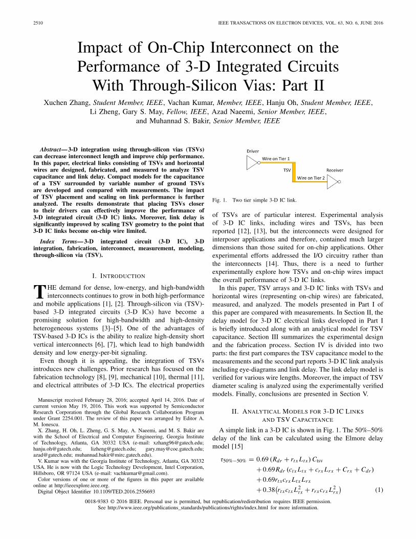
2510 IEEE TRANSACTIONS ON ELECTRON DEVICES, VOL. 63, NO. 6, JUNE 2016 Impact of On-Chip Interconnect on the Performance of 3-D Integrated Circuits With Through-Silicon Vias: Part II Xuchen Zhang, Student Member, IEEE, Vachan Kumar, Member, IEEE, Hanju Oh, Student Member, IEEE, Li Zheng, Gary S. May, Fellow, IEEE , Azad Naeemi, Senior Member, IEEE, and Muhannad S. Bakir, Senior Member, IEEE Abstract—3-D integration using through-silicon vias (TSVs) can decrease interconnect length and improve chip performance. In this paper, electrical links consisting of TSVs and horizontal wires are designed, fabricated, and measured to analyze TSV capacitance and link delay. Compact models for the capacitance of a TSV surrounded by variable number of ground TSVs are developed and compared with measurements. The impact of TSV placement and scaling on link performance is further analyzed. The results demonstrate that placing TSVs closer to their drivers can effectively improve the performance of 3-D integrated circuit (3-D IC) links. Moreover, link delay is significantly improved by scaling TSV geometry to the point that 3-D IC links become on-chip wire limited. Index Terms— 3-D integrated circuit (3-D IC), 3-D integration, fabrication, interconnect, measurement, modeling, through-silicon via (TSV). I. I NTRODUCTION T HE demand for dense, low-energy, and high-bandwidth interconnects continues to grow in both high-performance and mobile applications [1], [2]. Through-silicon via (TSV)- based 3-D integrated circuits (3-D ICs) have become a promising solution for high-bandwidth and high-density heterogeneous systems [3]–[5]. One of the advantages of TSV-based 3-D ICs is the ability to realize high-density short vertical interconnects [6], [7], which lead to high bandwidth density and low energy-per-bit signaling. Even though it is appealing, the integration of TSVs introduces new challenges. Prior research has focused on the fabrication technology [8], [9], mechanical [10], thermal [11], and electrical attributes of 3-D ICs. The electrical properties Manuscript received February 28, 2016; accepted April 14, 2016. Date of current version May 19, 2016. This work was supported by Semiconductor Research Corporation through the Global Research Collaboration Program under Grant 2254.001. The review of this paper was arranged by Editor A. M. Ionescu. X. Zhang, H. Oh, L. Zheng, G. S. May, A. Naeemi, and M. S. Bakir are with the School of Electrical and Computer Engineering, Georgia Institute of Technology, Atlanta, GA 30332 USA (e-mail: [email protected]; [email protected]; [email protected]; [email protected]; [email protected]; [email protected]). V. Kumar was with the Georgia Institute of Technology, Atlanta, GA30332 USA. He is now with the Logic Technology Development, Intel Corporation, Hillsboro, OR 97124 USA (e-mail: [email protected]). Color versions of one or more of the figures in this paper are available online at http://ieeexplore.ieee.org. Digital Object Identifier 10.1109/TED.2016.2556693 Fig. 1. Two tier simple 3-D IC link. of TSVs are of particular interest. Experimental analysis of 3-D IC links, including wires and TSVs, has been reported [12], [13], but the interconnects were designed for interposer applications and therefore, contained much larger dimensions than those suited for on-chip applications. Other experimental efforts addressed the I/O circuitry rather than the interconnects [14]. Thus, there is a need to further experimentally explore how TSVs and on-chip wires impact the overall performance of 3-D IC links. In this paper, TSV arrays and 3-D IC links with TSVs and horizontal wires (representing on-chip wires) are fabricated, measured, and analyzed. The models presented in Part I of this paper are compared with measurements. In Section II, the delay model for 3-D IC electrical links developed in Part I is briefly introduced along with an analytical model for TSV capacitance. Section III summarizes the experimental design and the fabrication process. Section IV is divided into two parts: the first part compares the TSV capacitance model to the measurements and the second part reports 3-D IC link analysis including eye-diagrams and link delay. The link delay model is verified for various wire lengths. Moreover, the impact of TSV diameter scaling is analyzed using the experimentally verified models. Finally, conclusions are presented in Section V. II. ANALYTICAL MODELS FOR 3-D IC LINKS AND TSV CAPACITANCE A simple link in a 3-D IC is shown in Fig. 1. The 50%–50% delay of the link can be calculated using the Elmore delay model [15] τ 50%−50% = 0.69 ( R dr + r tx L tx ) C tsv + 0.69 R dr (c tx L tx + c rx L rx + C rx + C dr ) + 0.69r tx c rx L tx L rx + 0.38 ( r tx c tx L 2 tx + r rx c rx L 2 rx ) (1) 0018-9383 © 2016 IEEE. Personal use is permitted, but republication/redistribution requires IEEE permission. See http://www.ieee.org/publications_standards/publications/rights/index.html for more information.
Transcript of 2510 IEEE TRANSACTIONS ON ELECTRON … of on-chip interconnect on...2510 IEEE TRANSACTIONS ON...
2510 IEEE TRANSACTIONS ON ELECTRON DEVICES, VOL. 63, NO. 6, JUNE 2016
Impact of On-Chip Interconnect on thePerformance of 3-D Integrated Circuits
With Through-Silicon Vias: Part IIXuchen Zhang, Student Member, IEEE, Vachan Kumar, Member, IEEE, Hanju Oh, Student Member, IEEE,
Li Zheng, Gary S. May, Fellow, IEEE, Azad Naeemi, Senior Member, IEEE,and Muhannad S. Bakir, Senior Member, IEEE
Abstract— 3-D integration using through-silicon vias (TSVs)can decrease interconnect length and improve chip performance.In this paper, electrical links consisting of TSVs and horizontalwires are designed, fabricated, and measured to analyze TSVcapacitance and link delay. Compact models for the capacitanceof a TSV surrounded by variable number of ground TSVsare developed and compared with measurements. The impactof TSV placement and scaling on link performance is furtheranalyzed. The results demonstrate that placing TSVs closerto their drivers can effectively improve the performance of3-D integrated circuit (3-D IC) links. Moreover, link delay issignificantly improved by scaling TSV geometry to the point that3-D IC links become on-chip wire limited.
Index Terms— 3-D integrated circuit (3-D IC), 3-Dintegration, fabrication, interconnect, measurement, modeling,through-silicon via (TSV).
I. INTRODUCTION
THE demand for dense, low-energy, and high-bandwidthinterconnects continues to grow in both high-performance
and mobile applications [1], [2]. Through-silicon via (TSV)-based 3-D integrated circuits (3-D ICs) have become apromising solution for high-bandwidth and high-densityheterogeneous systems [3]–[5]. One of the advantages ofTSV-based 3-D ICs is the ability to realize high-density shortvertical interconnects [6], [7], which lead to high bandwidthdensity and low energy-per-bit signaling.
Even though it is appealing, the integration of TSVsintroduces new challenges. Prior research has focused on thefabrication technology [8], [9], mechanical [10], thermal [11],and electrical attributes of 3-D ICs. The electrical properties
Manuscript received February 28, 2016; accepted April 14, 2016. Date ofcurrent version May 19, 2016. This work was supported by SemiconductorResearch Corporation through the Global Research Collaboration Programunder Grant 2254.001. The review of this paper was arranged by Editor A.M. Ionescu.
X. Zhang, H. Oh, L. Zheng, G. S. May, A. Naeemi, and M. S. Bakir arewith the School of Electrical and Computer Engineering, Georgia Instituteof Technology, Atlanta, GA 30332 USA (e-mail: [email protected];[email protected]; [email protected]; [email protected];[email protected]; [email protected]).
V. Kumar was with the Georgia Institute of Technology, Atlanta, GA 30332USA. He is now with the Logic Technology Development, Intel Corporation,Hillsboro, OR 97124 USA (e-mail: [email protected]).
Color versions of one or more of the figures in this paper are availableonline at http://ieeexplore.ieee.org.
Digital Object Identifier 10.1109/TED.2016.2556693
Fig. 1. Two tier simple 3-D IC link.
of TSVs are of particular interest. Experimental analysisof 3-D IC links, including wires and TSVs, has beenreported [12], [13], but the interconnects were designed forinterposer applications and therefore, contained much largerdimensions than those suited for on-chip applications. Otherexperimental efforts addressed the I/O circuitry rather thanthe interconnects [14]. Thus, there is a need to furtherexperimentally explore how TSVs and on-chip wires impactthe overall performance of 3-D IC links.
In this paper, TSV arrays and 3-D IC links with TSVs andhorizontal wires (representing on-chip wires) are fabricated,measured, and analyzed. The models presented in Part I ofthis paper are compared with measurements. In Section II, thedelay model for 3-D IC electrical links developed in Part Iis briefly introduced along with an analytical model for TSVcapacitance. Section III summarizes the experimental designand the fabrication process. Section IV is divided into twoparts: the first part compares the TSV capacitance model to themeasurements and the second part reports 3-D IC link analysisincluding eye-diagrams and link delay. The link delay model isverified for various wire lengths. Moreover, the impact of TSVdiameter scaling is analyzed using the experimentally verifiedmodels. Finally, conclusions are presented in Section V.
II. ANALYTICAL MODELS FOR 3-D IC LINKS
AND TSV CAPACITANCE
A simple link in a 3-D IC is shown in Fig. 1. The 50%–50%delay of the link can be calculated using the Elmore delaymodel [15]
τ50%−50% = 0.69 (Rdr + rt x Lt x) Ctsv
+ 0.69Rdr (ct x Lt x + crx Lrx + Crx + Cdr )
+ 0.69rt xcrx Lt x Lrx
+ 0.38(rt xct x L2
t x + rrx crx L2rx
)(1)
0018-9383 © 2016 IEEE. Personal use is permitted, but republication/redistribution requires IEEE permission.See http://www.ieee.org/publications_standards/publications/rights/index.html for more information.

ZHANG et al.: IMPACT OF ON-CHIP INTERCONNECT ON THE PERFORMANCE OF 3-D ICs 2511
Fig. 2. TSV capacitance circuit models showing the capacitance betweensignal and ground TSVs at (a) any frequency, (b) low frequency, and (c) highfrequency.
where Rdr and Cdr are the driver resistance and capacitance,respectively, rt x , ct x , and Lt x are the resistance per unit length,the capacitance per unit length, and the length of the on-chipwire on the driver side (Tier 1 in Fig. 1), respectively, and rrx ,crx and Lrx are the same for the on-chip wire on the receiverside (Tier 2 in Fig. 1). Ctsv is the capacitance of the TSV, andCrx is the load capacitance of the receiver.
The first term in (1), i.e., the delay due to the driver sideresistance combined with the TSV capacitance, dominates thetotal delay. Therefore, it is very important to understand andaccurately model the TSV capacitance.
A circuit model for two TSVs in a TSV array is shown inFig. 2(a). This model is simplified for low- and high-frequencycases. Due to the metal–insulator–semiconductor structure,TSVs may operate at either slow-wave mode or quasi-TEMmode depending on the frequency, TSV dimensions, andsubstrate resistivity [16]. When the operating frequency islower than 0.3 times the characteristic frequency of theslow-wave mode (0.3 fsw) [17], which is typically in thekilohertz and megahertz range, the TSV is in the slow-wavemode. In this mode, TSV capacitance is mainly determined byits oxide capacitance, which we define as the low-frequencycapacitance. As frequency increases, there is a transitionfrom the slow-wave mode to the quasi-TEM mode, allowingcomplete penetration of the E-field and H -field throughthe silicon substrate [17], [18]. In this mode, the TSVcapacitance is saturated by the silicon substrate capacitance Cc
in Fig. 2(c). In our simulation, the quasi-TEM mode isobserved at frequencies higher than ∼10 GHz (depending onTSV dimensions). In this mode, the overall TSV capacitanceis constant and equal to Cc. In this paper, we assume that thesubstrate is floating and is not biased during the measurement.
The admittance of the substrate between two TSVs can becalculated as [19]
Y = GC + j2π f Cc (2)
where GC is the substrate conductance and f is thefrequency of operation. At low frequencies, GC dominates theadmittance. Therefore, the substrate capacitance is shorted out,
Fig. 3. Experimental design for TSV capacitance and TSV-wire-TSV 3-D IClink measurements. (a) Design overview of TSV capacitance and 3-D IC linkmeasurements. (b) TSV capacitance design: one signal TSV with differentnumber of ground TSVs for TSV capacitance extraction. (c) 3-D IC linkdesign: the link with probing pads, TSVs, and wires on the back side.
reducing the model to the one shown in Fig. 2(b). As a result,the TSV capacitance to the substrate is approximately the TSVliner capacitance. Depending on the number of ground TSVssurrounding the signal TSV, including the pad capacitances,the effective low-frequency capacitance is given by
CLF = 1(
1NGNDCOX+CGPAD
)+
(1
COX+CSPAD
) (3)
where COX is the TSV liner capacitance, CGPAD is thecapacitance from the ground pad to the substrate, CSPAD is thecapacitance from the signal pad to the substrate, and NGND isthe number of ground TSVs surrounding the signal TSV.
At high frequencies, the capacitive admittance is muchlarger relative to the conductance of the substrate. As a result,the conductance of the substrate is ignored, as shownin Fig. 2(c). The substrate capacitance (Cc) for each ofthe TSV array configurations is estimated using SynopsysRaphael [20]. The effective high-frequency capacitance asa function of the TSV array configurations is given by
CHF = 1(
1 + 1NGND
) (1
COX
)+ 1
Cc
+ CSGPAD (4)
where CHF is the high-frequency capacitance, and CSGPAD isthe capacitance from the signal to ground pads.
III. EXPERIMENT DESIGN AND FABRICATION
Two design sets for the experimental evaluation of TSVs andon-chip wires are illustrated in Fig. 3. For TSV capacitanceextraction, single-port measurements are used, while forTSV-wire-TSV 3-D IC links, two-port measurements are used.The dimensions of all interconnect structures are summarizedin Table I.
A. TSV Capacitance Extraction
Six designs are fabricated to extract the capacitance ofTSVs, as shown in Fig. 4. Each design contains one signal

2512 IEEE TRANSACTIONS ON ELECTRON DEVICES, VOL. 63, NO. 6, JUNE 2016
TABLE I
DIMENSIONS OF STRUCTURES
Fig. 4. SEM images of six TSV sets with various number of ground TSVsranging from 0 to 8 (1S 0G indicates one signal TSV and zero ground TSV).
TSV in the center surrounded by various number of groundTSVs with a shorted probe pad. The first TSV design consistsof no ground TSVs to characterize the capacitance of the signalTSV to the ground pad as a reference to the other designs(top-left image of Fig. 4). The number of ground TSVs in thesecond through sixth designs is 2, 4, 4, 6, and 8, respectively.The third and fourth designs both have four ground TSVs,but their positions are different to compare diagonal TSVs tonearby TSVs. The impact of TSV pitch is also investigated byfabricating all six designs with TSV pitches of 50 and 100 μm.
B. 3-D IC Link
Coplanar waveguide configured ground-signal-ground wiresare used to emulate on-chip wires. The dimensions of thestructures were selected to emulate the electrical parametersof a 3-D IC link based on the ITRS 2013 report [21]. Thewire pitch is selected to be the same as the TSV pitch fordesign and analysis simplicity. Differing wire and TSV pitchesrequire fan-in/fan-out structures on both ends of the wire,which introduce discontinuities and impact the accuracy ofthe L-2L de-embedding.
The fabrication process begins with a 300-μm thickdouble-side polished silicon wafer. Silicon dioxide is depositedon the top side of the wafer using plasma-enhanced chemicalvapor deposition and patterned using dry etching. The siliconvias are then etched using the Bosch process with silicondioxide as the mask. Following the Bosch process, the waferis immersed in buffered oxide etchant to remove the silicondioxide. Next, a liner of silicon dioxide is thermally grown.A seed layer of titanium and copper is then deposited onthe back side using electron beam evaporation, followedby a bottom-up copper electroplating. The over-electroplatedcopper is removed by chemical-mechanical polishing to
Fig. 5. Overall fabrication process for TSV capacitance extraction and3-D IC link characterization.
Fig. 6. Images of the tested samples. (a) Front side of the sample on theprobing station, where the bright dots on the end of the probing pads are TSVs.(b) Back side of the sample with the fine wires. The surface of the sample isslightly damaged by chemical-mechanical polishing (CMP).
expose the TSVs. Finally, probe pads and wires are patternedon the front and back sides of the wafer, respectively. Thefabrication process is summarized in Fig. 5.
The overall wire thickness is 100 nm, including 30-nm-thicktitanium, 50-nm-thick copper, and 20-nm-thick gold. Opticalimages of the fabricated testbed are shown in Fig. 6.
IV. RESULT ANALYSIS
The fabricated testbed is measured using anAgilent N5245A network analyzer to obtain the S-parametersfrom 10 MHz to 50 GHz at a 250 MHz step. Single portS11 parameters are measured for TSV capacitance extraction.For 3-D IC link measurements, 2-port S-parameters aremeasured. The probe pads are de-embedded using L-2Lde-embedding [22]. Finally, the S-parameters are importedinto Keysight Advanced Design System (ADS) [23] to extractthe time-domain response of the links.
A. TSV Capacitance
For each of the TSV array configurations described inthe previous section, the experimentally obtained values ofcapacitance are compared with those extracted through HFSSand analytical/extracted models. Error bars are added tothe modeled capacitance to reflect TSV diameter variationof ±1 μm due to fabrication process variation.
ZHANG et al.: IMPACT OF ON-CHIP INTERCONNECT ON THE PERFORMANCE OF 3-D ICs 2513
Fig. 7. Low-frequency capacitance of different TSV array configurations.
Fig. 8. High-frequency capacitance of multiple TSV array configurations,for a TSV pitch of 100 μm.
Fig. 9. High-frequency capacitance of multiple TSV array configurations,for a TSV pitch of 50 μm.
The effective capacitance obtained through this modelis compared with experimental results. The error in thelow-frequency model is <17%, as shown in Fig. 7. At a TSVpitch of 100-μm and at high frequency, although the maximumerror is approximately 21% for structure 4, the trend ofcapacitance values is well matched between the model,simulation, and measurements, as shown in Fig. 8. For a TSVpitch of 50 μm, the model has an error of <5%, as shownin Fig. 9. It is worth noting that for all six structures, the50-μm pitch TSVs have larger high-frequency capacitance
Fig. 10. Measured S21 of TSV-wire-TSV links for five different wire lengths.
Fig. 11. Measured and simulated S21 before and after de-embedding forTSV-wire-TSV links with a wire length of 1 mm.
than the 100-μm pitch TSVs due to the larger impact ofsubstrate capacitance at high frequencies, which is consistentwith the result in [13].
B. 3-D IC Links
Five sets of links with different wire lengths are measured,and the results are shown in Fig. 10. The loss increases withfrequency and wire length as expected. It is evident that theloss of these links is large even at low frequency. The insertionloss of the 1-mm long link at 10 MHz is as high as −9.75 dB.This is due to the high dc resistance of the wires. It shouldalso be noted that the measurement of the 8-mm-long wireexhibits some noise, which is believed to be due to the smallvalues of S21.
The L-2L de-embedding method is adopted to eliminate theprobe pads [22]. Fig. 11 shows the originally measured S21,the de-embedded S21, and the values obtained via HFSSsimulations of a 3-D IC link. The HFSS simulations correlatewell with the measurements, with an average differenceof 1.25%.
After de-embedding the probe pads, the effective linkconsists of two TSVs interconnected with a wire, i.e., aTSV-wire-TSV link. Next, the TSVs are de-embedded toobtain the S-parameters of only the wire (TSVs on both sidesare de-embedded), the wire-TSV link (the TSV on the driver

2514 IEEE TRANSACTIONS ON ELECTRON DEVICES, VOL. 63, NO. 6, JUNE 2016
Fig. 12. Eye diagrams of four structures with different wire lengths.(a) 0.5 mm at data rate of 8 Gb/s. (b) 1 mm at 8 Gb/s. (c) 2 mm at 4 Gb/s.(d) 4 mm at 2 Gb/s.
Fig. 13. Eye diagrams of the four structures (a) wire only, (b) TSV-wire,(c) Wire-TSV, and (d) TSV-wire-TSV for 1-mm wire length at data rateof 8 Gb/s.
side is de-embedded), and the TSV-wire link (the TSV on thereceiver side is de-embedded).
The S-parameters are imported into Keysight ADS to extractthe eye diagram and delay. The driver resistance and receivercapacitance are from the ITRS 2013 14-nm node [21]. Theeye diagrams for wire-TSV links are shown in Fig. 12.At a data rate of 8 Gb/s, the eye is closed for links longerthan 2 mm. However, they can still achieve an eye-openingof 50% at lower bit rates, as shown Fig. 12(c) and (d). Fig. 13shows the impact of the TSV by comparing four structuresof the same wire length at a date rate of 8 Gb/s. Comparedwith the wire-TSV link shown in Fig. 13(c), the TSV-wire linkin Fig. 13(b) improves the eye opening from 510 to 650 mV.This demonstrates that the performance of the link is improvedwhen the TSV is placed closer to the driver. The reducedeye opening of the wire-TSV link is due to the interactionof the driver side wire resistance and the TSV capacitance.By placing the TSV closer to the driver, the driver side wireresistance becomes smaller, and therefore, a larger eye openingis achieved.
Fig. 14. Step response of (a) TSV-wire-TSV, wire-TSV, TSV-wire, and wireonly for 1-mm wire length and (b) five links with different wire length: 0.5,1, 2, 4, and 8 mm.
Fig. 15. Modeled and measured delay as a function of wire length.
Fig. 16. Impact of TSV geometry scaling on TSV capacitance and link delay.
Fig. 14(a) shows the step response of four links with thesame wire length. Compared with the wire only 50%–50%delay of 37.6 ps, the delay of the wire-TSV link is 53.9 ps,an increase of 43.4% due to the presence of the TSV. Movingthe TSV to the driver side (e.g., TSV-wire link) decreases thedelay to 44.5 ps, an improvement of 17.4% and an increaseof 18.4% compared with the wire only case. Fig. 14(b) showsthe response of the wire-TSV link for five different wirelengths.
The delay of the wire-TSV link at five different wire lengthsis modeled using the analytical model presented in Section IIand compared with measurements, as shown in Fig. 15. Foreach wire length, we measured two identical structures and theresults are marked as crosses. In the model, the wire resistance,wire capacitance, and TSV capacitance values are extracted

ZHANG et al.: IMPACT OF ON-CHIP INTERCONNECT ON THE PERFORMANCE OF 3-D ICs 2515
from the measurements. The maximum difference between themodeled and measured delays is approximately 8.5% at a wirelength of 8 mm. Even though the wires are longer than typicalon-chip wires, the time of flight was ignored in the model dueto the high resistance of the wires [24].
The impact of TSV geometry scaling on the TSVcapacitance and link delay is analyzed with the verifiedmodels, as shown in Fig. 16. In this analysis, the TSV aspectratio is assumed to be 10:1. Moreover, the silicon dioxide linerthickness is assumed to be 1/10 of the TSV diameter, and theM1 wire length is set to 10 μm. The link delay decreasessignificantly as the TSV diameter decreases. When the TSVdiameter scales below 1 μm, the link delay becomes saturated.This is because the TSV capacitance becomes comparablewith the on-chip wire capacitance, and the delay begins tobe dominated by the on-chip wires.
V. CONCLUSION
In this paper, TSV arrays and 3-D IC links with TSVsand horizontal wires are fabricated, measured, and analyzed.The TSV capacitance and link delay models are verified withmeasurements. It is shown that the TSV capacitance and thedriver side wire resistance can dominate the link performanceand could potentially be the key bottleneck for digital 3-D ICs.The delay and eye opening of the link can be significantlyimproved by placing TSVs closer to their drivers. As presentedin Part I and Part II, reducing the length of on-chip wires andheight and diameter of the TSVs have a significant impact on3-D IC link performance.
REFERENCES
[1] T. O. Dickson et al., “An 8 × 10-Gb/s source-synchronous I/O systembased on high-density silicon carrier interconnects,” IEEE J. Solid-StateCircuits, vol. 47, no. 4, pp. 884–896, Apr. 2012.
[2] M. H. Jabbar, D. Houzet, and O. Hammami, “3D multiprocessor with3D NoC architecture based on Tezzaron technology,” in Proc. IEEE Int.3D Syst. Integr. Conf. (3DIC), Jan./Feb. 2012, pp. 1–5.
[3] J. U. Knickerbocker et al., “3-D silicon integration and silicon packagingtechnology using silicon through-vias,” IEEE J. Solid-State Circuits,vol. 41, no. 8, pp. 1718–1725, Aug. 2006.
[4] Y. Zhang, L. Zheng, and M. S. Bakir, “3-D stacked tier-specificmicrofluidic cooling for heterogeneous 3-D ICs,” IEEE Trans. Compon.,Packag., Manuf. Technol., vol. 3, no. 11, pp. 1811–1819,Nov. 2013.
[5] H. Kim et al., “Measurement and analysis of a high-speed TSVchannel,” IEEE Trans. Compon., Packag., Manuf. Technol., vol. 2, no. 10,pp. 1672–1685, Oct. 2012.
[6] M. S. Bakir et al., “3D heterogeneous integrated systems: Liquidcooling, power delivery, and implementation,” in Proc. IEEE CustomIntegr. Circuits Conf. (CICC), Sep. 2008, pp. 663–670.
[7] Y. Madhour, S. Zimmermann, J. Olivier, J. Thome, M. Bruno, andD. Poulikakos, “Cooling of next generation computer chips: Parametricstudy for single- and two-phase cooling,” in Proc. IEEE 17th Int.Workshop Thermal Invest. ICs Syst. (THERMINIC), Sep. 2011, pp. 1–7.
[8] Q. Chen, C. Huang, D. Wu, Z. Tan, and Z. Wang, “Ultralow-capacitancethrough-silicon vias with annular air-gap insulation layers,” IEEE Trans.Electron Devices, vol. 60, no. 4, pp. 1421–1426, Apr. 2013.
[9] P. A. Thadesar and M. S. Bakir, “Novel photo-defined polymer-enhanced through-silicon vias for silicon interposers,” IEEE Trans.Compon., Packag., Manuf. Technol., vol. 3, no. 7, pp. 1130–1137,Jul. 2013.
[10] C. Okoro, J. W. Lau, F. Golshany, K. Hummler, and Y. S. Obeng,“A detailed failure analysis examination of the effect of thermal cyclingon Cu TSV reliability,” IEEE Trans. Electron Devices, vol. 61, no. 1,pp. 15–22, Jan. 2014.
[11] X. Zhang et al., “3D IC with embedded microfluidic cooling:Technology, thermal performance, and electrical implications,” inProc. Int. Tech. Conf. Exhibit. Packag. Integr. Electron. Photon.Microsyst., 13th Int. Conf. Nanochannels, Microchannels,Minichannels (InterPACKICNMM), Jul. 2015, p. V003T10A008.
[12] J. Kim et al., “High-frequency scalable electrical model and analysis ofa through silicon via (TSV),” IEEE Trans. Compon., Packag., Manuf.Technol., vol. 1, no. 2, pp. 181–195, Feb. 2011.
[13] J. Kim et al., “High-frequency scalable modeling and analysis of adifferential signal through-silicon via,” IEEE Trans. Compon., Packag.,Manuf. Technol., vol. 4, no. 4, pp. 697–707, Apr. 2014.
[14] Y. Liu, W. Luk, and D. Friedman, “A compact low-power 3D I/O in45 nm CMOS,” in Proc. IEEE Int. Solid-State Circuits Conf. (ISSCC),Feb. 2012, pp. 142–144.
[15] J. Rubinstein, P. Penfield, and M. A. Horowitz, “Signal delay in RCtree networks,” IEEE Trans. Comput.-Aided Design Integr., vol. 2, no. 3,pp. 202–211, Jul. 1983.
[16] J. S. Pak et al., “Slow wave and dielectric quasi-TEM modes ofmetal-insulator-semiconductor (MIS) structure through silicon via (TSV)in signal propagation and power delivery in 3D chip package,” inProc. IEEE 60th Electron. Compon. Technol. Conf. (ECTC), Jun. 2010,pp. 667–672.
[17] I. Ndip et al., “High-frequency modeling of TSVs for 3-D chip integra-tion and silicon interposers considering skin-effect, dielectric quasi-TEMand slow-wave modes,” IEEE Trans. Compon., Packag., Manuf. Technol.,vol. 1, no. 10, pp. 1627–1641, Oct. 2011.
[18] H. Hasegawa, M. Furukawa, and H. Yanai, “Properties of microstripline on Si-SiO2 system,” IEEE Trans. Microw. Theory Techn., vol. 19,no. 11, pp. 869–881, Nov. 1971.
[19] C. Xu, H. Li, R. Suaya, and K. Banerjee, “Compact AC modeling andperformance analysis of through-silicon vias in 3-D ICs,” IEEE Trans.Electron Devices, vol. 57, no. 12, pp. 3405–3417, Dec. 2010.
[20] Synopsys Raphael, accessed on Sep. 2014. [Online]. Available: http://www.synopsys.com/TOOLS/TCAD/INTERCONNECTSIMULATION/Pages/Raphael.aspx
[21] ITRS 2013 Tables, accessed on Oct. 2014. [Online]. Available:http://www.itrs.net
[22] H.-T. Yen et al., “TSV RF de-embedding method and modelingfor 3DIC,” in Proc. IEEE Annu. SEMI Adv. Semiconductor Manuf.Conf. (ASMC), May 2012, pp. 394–397.
[23] Keysight ADS, accessed on Oct. 2014. [Online]. Available:http://www.keysight.com/en/pc-1297113/advanced-design-system-ads?cc=US&lc=eng
[24] R. Venkatesan, J. A. Davis, and J. D. Meindl, “Compact distributed RLCinterconnect models—Part IV: Unified models for time delay, crosstalk,and repeater insertion,” IEEE Trans. Electron Devices, vol. 50, no. 4,pp. 1094–1102, Apr. 2003.
Xuchen Zhang (S’15) received the B.S. degreein electronics engineering and the M.S. degree inmicroelectronics from Shanghai Jiao Tong Univer-sity, Shanghai, China, in 2008 and 2011, respec-tively, and the M.S. degrees in electrical engineeringfrom the Georgia Institute of Technology, Atlanta,GA, USA, in 2012, where he is currently pursuingthe Ph.D. degree.
His current research interests include 3-D elec-tronic system integration, advanced packaging, andembedded micro-fluidic cooling.
Vachan Kumar (S’10–M’14) received the B.E.degree in electronics and communication engineer-ing from the National Institute of Technology Kar-nataka, Surathkal, India, in 2006, and the M.S. andPh.D. degrees in electrical and computer engineeringfrom the Georgia Institute of Technology, Atlanta,GA, USA, in 2012 and 2014, respectively.
He is currently with Logic Technology Develop-ment, Intel Corporation, Portland, OR, USA, wherehe is involved in technology benchmarking.

2516 IEEE TRANSACTIONS ON ELECTRON DEVICES, VOL. 63, NO. 6, JUNE 2016
Hanju Oh (S’14) received the B.S. degree inelectrical and computer engineering from HanyangUniversity, Seoul, South Korea, in 2010, and theM.S. degree from the Georgia Institute of Tech-nology, Atlanta, GA, USA, in 2014, where he iscurrently pursuing the Ph.D. degree in electrical andcomputer engineering.
Li Zheng received the B.S. degree from ZhejiangUniversity, Hangzhou, China, in 2006, the M.S.degree from Shanghai Jiao Tong University,Shanghai, China, in 2009, and the Ph.D. degreein electrical and computer engineering from theGeorgia Institute of Technology, Atlanta, GA, USA,in 2015.
His current research interests include advanced3-D packaging, numerical power distributionnetwork modeling, and microfluidic cooling forhigh-performance computing systems.
Gary S. May (S’83–M’91–SM’97–F’06) receivedthe B.S. degree in electrical engineering from theGeorgia Institute of Technology (Georgia Tech),Atlanta, GA, USA, in 1985, and the M.S. andPh.D. degrees in electrical engineering and com-puter science from the University of California atBerkeley, Berkeley, CA, USA, in 1987 and 1991,respectively.
He is currently the Dean of the College of Engi-neering with Georgia Tech.
Azad Naeemi (S’99–M’04–SM’04) received theB.S. degree in electrical engineering from SharifUniversity, Tehran, Iran, in 1994, and the M.S. andPh.D. degrees in electrical and computer engineeringfrom the Georgia Institute of Technology (GeorgiaTech), Atlanta, GA, USA, in 2001 and 2003,respectively.
He joined as a Faculty Member with the School ofElectrical and Computer Engineering, Georgia Tech,where he is currently an Associate Professor.
Muhannad S. Bakir (SM’12) received theB.E.E. degree from Auburn University, Auburn, AL,USA, in 1999, and the M.S. and Ph.D. degrees inelectrical and computer engineering from the Geor-gia Institute of Technology (Georgia Tech), Atlanta,GA, USA, in 2000 and 2003, respectively.
He is currently an Associate Professor with theSchool of Electrical and Computer Engineering,Georgia Tech.