250=kW CW Klystron Amplifier for Planetary Radar · 1 TDA Progress Report 42-108 I February 15,...
13
1 TDA Progress Report 42-108 I February 15, 1992 250=kW CW Klystron Amplifier for Planetary Radar R. Cormier Radio Frequency and Microwave Subsystems Section A. Mizuhara Microwave Power Tube Products, Varian Associates, Inc. Palo Alto, California This article describes the design, construction, and performance testing of two Varian klystrons, model VKX-7864A, which replaced the aging and less efficient VA-949J klystrons in the X-band planetary radar transmitter on the Goldstone, California, 70-meter antenna. The project was carried out jointly by the Jet Propul- sion Laboratory and Varian Associates. Output power was increased from 200 kW to 250 kW continuous wave per klystron, and full dc beam power is dissipated in the collector (it was not possible to operate the VA-949J klystrons without R F drive because of limited collector dissipation capability). Replacements were made with a minimum of transmitter modifications. The planetary radar transmitter is now operating successfully with these two klystrons. 1. Introduction The X-band planetary radar transmitter at the Deep Space Network tracking facility at Goldstone, California, has been in operation since 1974. The planetary radar provided the first topological map of planet Venus. Valu- able information has also been gained from radar echoes obtained from the planets Mercury, Mars, Jupiter, and Saturn, from the moons of Jupiter and Saturn, including the rings of Saturn and possible rings of Earth (see this issue), and from nearby asteroids. The transmitter contains two klystrons operating in parallel to generate the output power. In 1986, a study contract was placed with Varian for a klystron of new de- sign, Varian’s model VI<X-7864A,to replace the aging, less efficient, low-reliability, and lower power klystrons, Var- ian’s model VA-949J. In April 1991, installation of the two newly designed klystrons upgraded the transmitter system to an output power of 450 kW and an operating center fre- quency of 8510 MHz. The VA-949J has a yoke-type electromagnet. Since the collector coil slips over the collector during mount- ing, the collector diameter is limited. Dissipation of full dc beam power requires a much larger collector, which re- quires redesign of the electromagnet to a solenoid. With a solenoid-type electromagnet, the klystron is installed gun- first, which allows the collector to be independently sized. The disadvantage is the extreme dimensional accuracy re- quired in construction of the solenoid to realize alignment 201 https://ntrs.nasa.gov/search.jsp?R=19920015073 2018-07-26T23:22:26+00:00Z
-
Upload
nguyenngoc -
Category
Documents
-
view
226 -
download
0
Transcript of 250=kW CW Klystron Amplifier for Planetary Radar · 1 TDA Progress Report 42-108 I February 15,...

1 TDA Progress Report 42-108 I
February 15, 1992
250=kW CW Klystron Amplifier for Planetary Radar R. Cormier
Radio Frequency and Microwave Subsystems Section
A. Mizuhara Microwave Power Tube Products, Varian Associates, Inc.
Palo Alto, California
This article describes the design, construction, and performance testing of two Varian klystrons, model VKX-7864A, which replaced the aging and less efficient VA-949J klystrons in the X-band planetary radar transmitter on the Goldstone, California, 70-meter antenna. The project was carried out jointly by the Jet Propul- sion Laboratory and Varian Associates. Output power was increased from 200 k W to 250 kW continuous wave per klystron, and full dc beam power is dissipated in the collector (it was not possible to operate the VA-949J klystrons without R F drive because of limited collector dissipation capability). Replacements were made with a minimum of transmitter modifications. The planetary radar transmitter is now operating successfully with these two klystrons.
1. Introduction The X-band planetary radar transmitter at the Deep
Space Network tracking facility at Goldstone, California, has been in operation since 1974. The planetary radar provided the first topological map of planet Venus. Valu- able information has also been gained from radar echoes obtained from the planets Mercury, Mars, Jupiter, and Saturn, from the moons of Jupiter and Saturn, including the rings of Saturn and possible rings of Earth (see this issue), and from nearby asteroids.
The transmitter contains two klystrons operating in parallel to generate the output power. In 1986, a study contract was placed with Varian for a klystron of new de- sign, Varian’s model VI<X-7864A, to replace the aging, less
efficient, low-reliability, and lower power klystrons, Var- ian’s model VA-949J. In April 1991, installation of the two newly designed klystrons upgraded the transmitter system to an output power of 450 kW and an operating center fre- quency of 8510 MHz.
The VA-949J has a yoke-type electromagnet. Since the collector coil slips over the collector during mount- ing, the collector diameter is limited. Dissipation of full dc beam power requires a much larger collector, which re- quires redesign of the electromagnet to a solenoid. With a solenoid-type electromagnet, the klystron is installed gun- first, which allows the collector to be independently sized. The disadvantage is the extreme dimensional accuracy re- quired in construction of the solenoid to realize alignment
201
https://ntrs.nasa.gov/search.jsp?R=19920015073 2018-07-26T23:22:26+00:00Z

between the magnetic field and the electron beam. As a result, the klystron body must be as short as possible, but not so short that the required gain and efficiency cannot be met.
The increased klystron output power to 250 kW places severe demands on the cooling of cavities and cavity tuners, especially output and penultimate cavities. The initial paper design had an extended interaction output circuit, but at the end of the design phase, Varian con- cluded with JPL concurrence that for this application a single-gap output circuit using an innovative cooling a p proach was simpler and more cost-effective. The addition of a prepenultimate cavity and the tuning of cavities for maximum efficiency resulted in a 45-percent efficiency.
I I . Description of the VKX-7864A Klystron Amplifier Design requirements for this klystron amplifier tube are
a saturated gain of 50 dB, a bandwidth of 40 MHz (-1 dB points), and an electronic efficiency of 45 percent. The tube delivers 250 kW at a frequency of 8510 hlHz, which is 15 MHz higher than the previous operating frequency of the planetary radar. Operating frequency band edges are from 8500 to 8520 MHz, with a power variation over the 20 hlHz of 0.25 dB. A beam-current requirement of 11.5 A maximum was constrained by existing equipment a t the tracking facility. The tube was required to fit into the existing socket and cabinet assemblies used for the VA- 949J.
Primary emphasis has been on improving reliability of the klystron amplifier. A reduction of maximum elec- tric field gradient in the gun region from 140 kV/cm to 90 kV/cm eliminated arcing problems experienced in the VA-949J. Decrease of cathode loading and coating the cathode with a binary alloy lowered cathode temperature and the barium evaporation rate by a factor of four. Tube length was minimized to reduce size and weight, since a longer tube requires a heavier focusing solenoid assembly. The VKX-7864A has a Pierce-type electron gun, six cav- ities, and a collector. Since the available beam supply is current limited, the klystron gun was designed to operate within the limits of this supply.
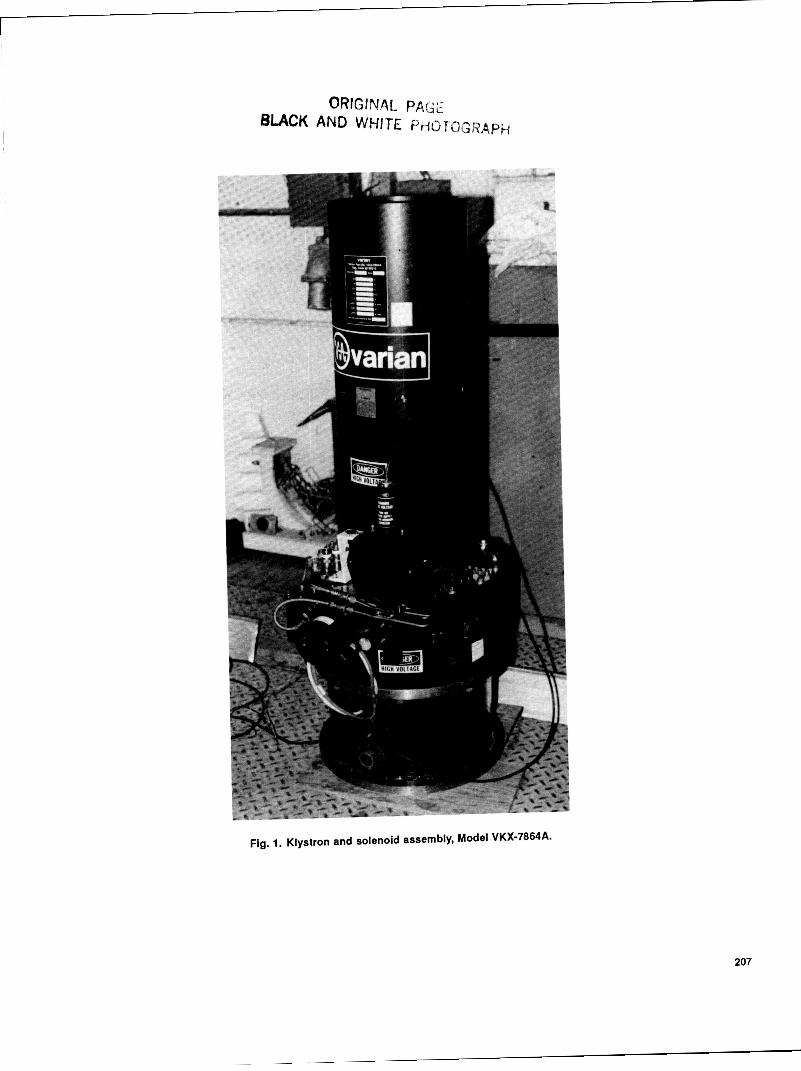
Figure 1 is a photograph of the klystron mounted in its solenoid and sitting in its stand. The klystron has an appendage vacuum pump for monitoring gas pressure inside the tube.
A. Electron Gun
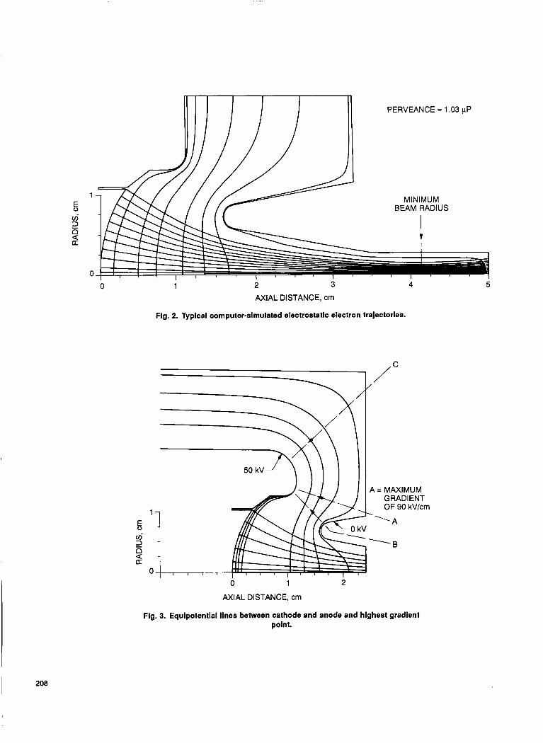
Figure 2 is a computer-simulated model of electrostatic electron trajectories, and shows a final cathode-to-beam area convergence of about 37:l. The figure is a sectional view of the axially symmetric electron gun with only the upper half shown. Electrons emitted from the cathode converge a t a place identified on the figure as “minimum beam radius.” Equipotential lines are shown transverse to electron paths. Figure 3 is similar to Fig. 2 except that electric field gradients were taken as shown at points A, B, and C. From the electric field distribution around the axially symmetric diode gun, a maximum gradient of 90 kV/cm occurs on the focus electrode a t point A in the figure. The earlier VA-949J klystron had a maximum gra- dient of 140 kV/cm and consequently required very long dc aging periods.
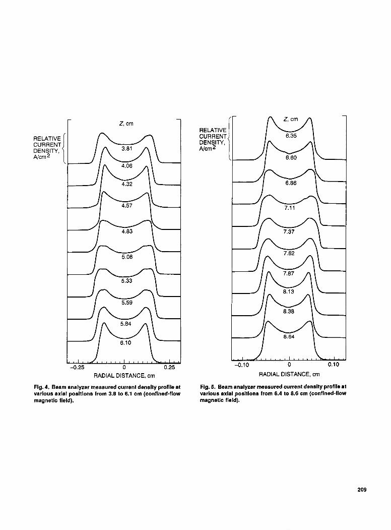
Having produced an electrostatic beam of correct pur- veyance and minimum diameter, the next step was the design of a magnetic field to maintain the beam with an ac- ceptable degree of scalloping, and verification testing in the beam analyzer. A scaled model of this gun was fabricated for testing in the beam analyzer. The beam analyzer gives a cross-sectional measurement of current density along the axis of the actual electron beam. Minor adjustments of magnetic field reduced scalloping from 12 percent to 7 per- cent. Figures 4 and 5 show beam-analyzer measurements of the current density profile at various axial distances from the gun pole piece aperture reference plane (in the Z-axis direction).
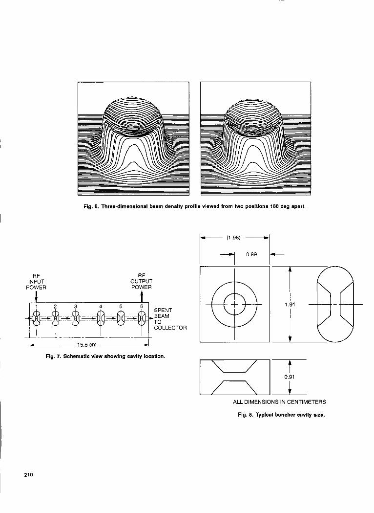
Figure 6 shows two views 180 deg apart of a computer- drawn perspective of the beam’s cross-sectional current density based on beam-analyzer data. It exhibits normal current density tapering from 4 A/cm2 at cathode edge to 2 A/cm2 on axis. Minor perturbations in current den- sity indicate patchy emission quality of the cathode’s emit- ting surface near its axis. These perturbations disappeared with proper aging.
B. Klystron Body
The new klystron consists of an input cavity, four buncher cavities, and an output cavity. The RF signal to be amplified at the input cavity starts the velocity modu- lation process. The field free space between cavities allows the beam to drift and form bunches. Each subsequent cavity couples to the beam, reinforcing bunching energy. The output cavity couples energy from the beam to the output waveguide. Cavities 1, 2, and 3 are stagger-tuned to achieve the required flat bandpass response. Cavities 4 and 5 are tuned for efficiency at a frequency above the high-band edge, enhancing bunching action of the beam.
202
Cavity 6, the output cavity, is always tuned to center fre- quency. A schematic view of the six cavities is shown in Fig. 7, and typical buncher cavity dimensions are shown in Fig. 8.
A coaxial-tewaveguide transition with a matching cou- pling iris between waveguide and input cavity provides a low voltage standing-wave ratio (VSWR) load to the input signal. A ceramic vacuum window with a coupling probe isolates the vacuum of the input cavity from the air side of the coaxial coupler. The probe converts the TEM coax- ial mode into the TElO waveguide mode for coupling to the input cavity. The size of the coupling iris matches the impedance of the cavity to the waveguide. For a cavity gap spacing of 1.0 radian, a beam Q of 321, and a cold unloaded Q of 3500, the external Q equals 294. Use of a coaxial input makes it easier for the input line to exit through the solenoid-type electromagnet.
The beam coupling coefficient for a gridded gap M = sin(wTo/2)/wTo/2 measures the ratio of ac current induced in the cavities to the ac component of the electron beam. For most klystrons, the gaps are not gridded and the beam coupling coefficient is more complex, involving electric and magnetic field geometry a t the cavity gap. The ratio of gap spacing to electron velocity, d / v = To, determines the time electrons remain in transit in the cavity gap. The product of the characteristic impedance of cavities (Rshunt/Q) and the beam coupling coefficient squared was maximized to yield the specified saturated gain of 50 dB; both are depen- dent on cavity gap spacing. Characteristic impedance of a cavity increases as gap spacing increases, while the beam coupling coefficient decreases with increased gap spacing. For this klystron, the value of the coupling coefficient equals about 0.7 and the characteristic cavity impedance equals 108 ohms. The optimum product of characteristic impedance and the beam coupling coefficient squared gives a gap spacing of 1.2 radians.
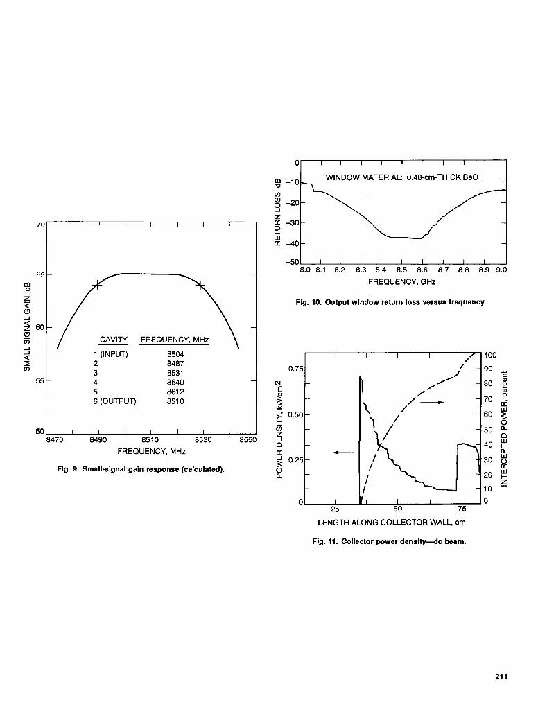
The final design is a compromise to meet or exceed all design goals simultaneously: RF power output, gain, bandwidth, and efficiency. From proprietary small-signal and large-signal computer programs, spacing between cav- ities as well as cavity external Q and frequency were found. Tuning based on calculated small-signal gain response, shown in Fig. 9, was later modified in hot test to opti- mize output power and efficiency.
The efficiency depends mostly on the tuned frequency of prepenultimate and penultimate cavities. A prepenulti- mate cavity complicates the problem of finding optimum tuning. The process involved systematic mapping of large- signal RF response by holding the frequency of one cavity
constant while varying another. This also must be done with cavity 3 as a parameter. The efficiency of the fabri- cated tube measured 45 percent , the design value specified.
Temperature variations of the buncher cavities cause the frequency of cavities to change. A cold test of a cav- ity measured a straight line slope of -0.158 MHz/deg C. Because these tubes at the transmitter site in the Mohave Desert experience a normal coolant temperature variation of about 30 deg C from midmorning to early afternoon, cavity frequency can change at a rate of 0.5 to 1 MHz per hour. Corresponding phase change would be intolerable, especially when the transmit-receive cycle may be several hours. Consequently, it is necessary to have a dedicated, temperature-regulated coolant supply for the klystron RF (cavity) circuit and output waveguide.
Thermal design is a critical part of klystron design. Very tight coupling of cooling water to cavities is neces- sary to remove heat generated by the RF on the walls of cavities. Although cavities are not tunable in operation, during initial testing a t Varian the cavities required tuners. Use of a diaphragm tuner on the cavity wall complicates the cooling design. In fact, the initial prototype tube failed because of inadequate cooling of the penultimate cavity di- aphragm tuner. The solution consisted of an increase in thickness of the diaphragm to provide better heat conduc- tivity and a modification of the cooling pipe to provide better thermal coupling to the diaphragm.
As a result of bunching, minimum electron velocity is an important parameter in preventing excessive body in- tercept current. Typically, it is prudent to design for the slowest electron velocity to be no lower than 20 percent of dc beam velocity. During testing, body current (beam current intercepted by the body circuit, which is primarily at the output cavity) tripled when phase modulated. Orig- inally, the body current overload was to be set to 30 mA but, because of the increase in current due to phase modu- lation, a new value of 60 mA was selected. However, when measured calorimetrically, both with and without modu- lation, the body power remained nearly unchanged, which implies that the energy of additional electrons intercepted with modulation is negligible. This increase in body cur- rent is believed to result from those sidebands (created by the modulating process), which add in-phase to generate a higher gap voltage. A higher retarding gap voltage would tend to strip off slower electrons in the bunched beam at the output cavity. The drawback of this increased body current is the necessity of setting body current interlock protection to twice the preferred value. This increases the risk of potential damage from overheating due to a fault when the carrier is not modulated.
203

C. Window
The output window is a thick-block (typically a half- wavelength) round window. The material is beryllium oxide ceramic. A cooling jacket surrounds and supports the window. Output VSWR return loss versus frequency, shown in Fig. 10, is the result of measured data on a win- dow before the window was mounted to the klystron. With 250 kW of output power, window dissipation is 800 W.
D. Collector
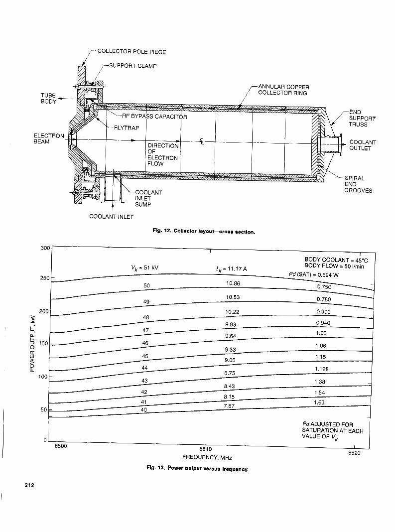
The collector is an oxygen-free high-conductivity cop- per cylinder with a closed top. The inside diameter is 20 cm. Liquid coolant passes through holes in the walls to cool the 2.5-cm-thick sidewalls. The beam spreads in the collector due to the repulsive force of electrons on each other. Lack of a magnetic field allows electrons to spread freely. When there is no RF on the beam, full beam power must be dissipated in the collector. From Fig. 11 the peak power density for the dc beam is 670 W/cm. This occurs where the beam first impinges on the collector. The in- tercepted beam power has a narrow and very sharp peak, which allows the copper to conduct heat to surrounding ar- eas. Nevertheless, wall temperature at the cooling passage could cause coolant boiling if coolant pressure were near atmospheric. To prevent boiling, this area is connected to the inlet or high-pressure side of the heat exchanger (nom- inally 8.5 kg/cm2). When the klystron is producing RF, collector power is reduced by the RF output power and the beam spreads faster than a dc beam. Although some electrons have greater velocities upon entering the collec- tor, the majority have lower velocities. Slower electrons tend to impinge the collector surface in a zone preceding the point where a dc beam first strikes. With an output power of 270 kW, the maximum peak power density is 120 iV/cm2.
The collector end cooling device contains spiral grooves. Figure 12 shows a cross section of the collector assembly. In the final assembly, a thin lead wrap on the collector serves as an X-ray shield.
E. Magnetic Focusing
A reentrant solenoid focuses the electron beam. This type of solenoid is necessary because of the large size of the collector. During installation, the klystron is lowered into the solenoid gun-first, until the collector pole piece rests on the solenoid outer cylinder. The collector is above the electromagnet, and the collector size is completely in- dependent of the solenoid. The solenoid requires tight di- mensional accuracy and serves to shield sgainst any X-rays generated in the klystron body.
The minimum field required to focus a dc beam of con- stant axial velocity, current density, and radius is called the Brillouin field. Because of the need to keep inter- cepted body current to an absolute minimum under RF conditions, the magnetic field must be about 2.7 times the Brillouin value. The magnetic field leaks into the cath- ode region for convergent flow focusing. Except for the small leakage field in the cathode region, construction of the solenoid is such that it is fully magnetically shielded. The solenoid is 46 cm in diameter and 23 cm high and weighs about 122 kg. The total weight of klystron and magnet is 333 kg.
111. Performance Measurements Test data measured on the first two klystrons fabri-
cated have characteristics so close to each other that with both tubes operating from a common beam power supply, transmission and combining losses are within 0.5 dB. The data presented here are not from one klystron. Some test results are from klystron Serial Number 101, while other results are from Serial Number 102.
A. Bandpass
The klystron operating frequency is from 8500 to 8520 MHz, and bandpass data, shown in Fig. 13, are lim- ited to this frequency range. Bandpass curves are for beam voltages of 40 to 51 kV, with the drive adjusted to provide saturated output at each value of beam volt- age. At 51 kV the output power at 8510 MHz is 260 kW with a variation of -0.25 dB at band edges. Because the output cavity is for all practical purposes untunable, the resonant frequency of the output cavity turned out to be about 7 MHz lower than the desired center frequency of 8510 MHz. However, required minimum output power of 250 kW at 8510 MHz was still met with a 51-kV beam because of the relatively flat response.
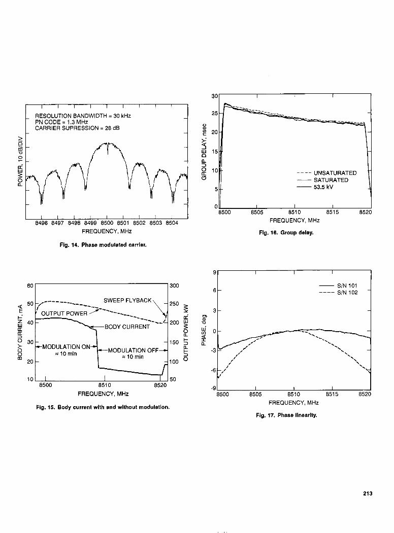
As previously stated, one problem experienced was an increase of body current with phase modulation. With a modulated signal at the input to the klystron (Fig. 14), the switching of modulation from on to off causes an abrupt change of body current, as seen in Fig. 15. With mod- ulation, body current was 42 mA at a carrier frequency of 8500 MHz; at 8510 MHz when modulation was turned off, body current suddenly decreased by 20 mA. Figure 15 shows that there was no change of output RF power at the time of switching modulation. The switching of modula- tion and the accompanying sudden change in body cur- rent was observed while slowly sweeping the frequency from 8500 to 8520 MHz. Subsequently, the klystron body
204
was instrumented for measuring power dissipation and the power does not change with or without modulation. This result confirms that increased body current does not con- tribute additional power dissipation in the cavities of the klystron.
B. Group Delay and Phase Linearity
Group delay remains practically unchanged with the klystron operating saturated or unsaturated, as shown in Fig. 16. Group delay data taken at a beam voltage of 53.5 kV, which is 2.3 kV above normal operating value, are also shown in Fig. 16. This value of voltage was used to ex- amine the sensitivity of group delay to variations of beam voltage. The group delay remains practically unchanged with variations in output power and operating beam volt- age. Variations are attributed to instrument noise. The output phase linearity is shown in Fig. 17.
C. Phase Pushing Factors
Phase pushing factors are listed in Table 1. The coolant temperature caused a larger change in phase than what was specified. During initial testing at Varian, a com- mon coolant line for the klystron body and waveguide was used, and phase changes were associated with tempera- ture changes of klystron body and waveguides. Varying the collector coolant temperature had no measurable ef- fects on phase. For the WR-125 waveguide operating a t 8510 MMz, the phase changes with a temperature equal to 0.21 deg/deg C per meter of waveguide length. It is known that the phase pushing factor is negative for the klystron and positive for the waveguide. The coolant is stabilized to better than &l deg C; consequently, the phase pushing factor, although much greater than originally specified, is not a problem.
IV. Conclusion The first two VKX-7864A klystrons tested met the re-
quirements as replacements for the VA-949J klystrons in the planetary radar transmitter. These new tubes are now operating in parallel at Deep Space Station 14, Goldstone, California. Combined output power from the two VKX- 7864A’s is about 500 kW, but because of losses due to com- bining and waveguide transmission, radiated power at the feedhorn is 450 kW. This value of radiated power is about 100 kW more than that available from the VA-949J’s. The collector of each klystron is able to dissipate full dc beam power, which greatly simplifies radar detection and analy- sis of near-Earth asteroids and man-made debris.
These two tubes have very close characteristics, allow- ing operation from a common beam supply. Both tubes have nearly identical bandpass and gain responses as well as group delay and phase linearity across the band of in- terest. The phase pushing factors as a function of var- ious operating parameters met their requirements in all cases except for that of body coolant temperature. Use of a temperature-regulated coolant source for body and waveguide would have been required even with the lower pushing factor. The higher pushing factor of the body is acceptable.
The only other unexpected phenomenon, increased body current with phase modulation, proved to be in- significant because the intercepted electrons have little ki- netic energy and do not add to body thermal dissipation. These klystrons represent state of the art for X-band CW klystron amplifiers.
205
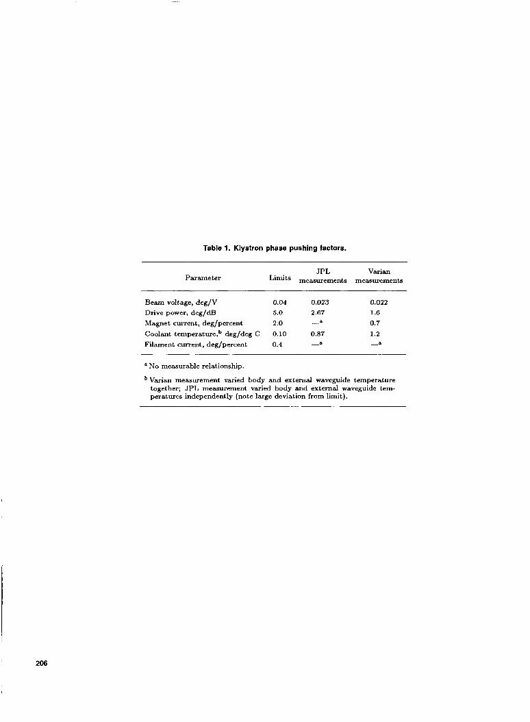
Table 1. Klystron phase pushing factors.
JPL Varian Parameter Limits measurements measurements
~
Beam voltage, deg/V 0.04 0.023 0.022
Magnet current, deg/percent 2.0 Coolant temperature,b deg/deg C 0.10 0.87 1.2
Drive power, deg/dB 5.0 2.67 1.6
0.7 a -
a -a - Filament current, deg/percent 0.4
a No measurable relationship.
bVarian measurement varied body and external waveguide temperature together; JPL measurement varied body and external waveguide tem- peratures independently (note large deviation from limit).
ORIGINAL PAGE BLACK AND WHf TE P d O iOGRApH
Fig. 1. Klystron and solenoid assembly, Model VKX-7864A.
207
E,
PERVEANCE = 1.03 pP
MINIMUM BEAM RADIUS
4 5 2 3
AXIAL DISTANCE, cm
1 0
Fig. 2. Typical computer-simulated electrostatic electron trajectories.
/ / c
A = MAXIMUM GRADIENT OF 90 kV/cm .
‘A . .
‘B
0 1 2
AXIAL DISTANCE, cm
Fig. 3. Equipotential lines between cathode and anode and hlghest gradient point.
I 208
RELATIVE CURRENT DENSITY, A/cm2
Z, cm
-0.25 0 0.25 RADIAL DISTANCE, cm
Fig. 4. Beam analyzer measured current density profile at various axle1 positions from 3.8 to 6.1 cm (confined-flow magnetic field).
I RELATIVE CURRENT DENSITY, Ncm2
-0.10 0 0.10
RADIAL DISTANCE, cm
Fig. 5. Beam analyzer measured current density profile at various axial positions from 6.4 to 8.6 cm (confined-flow magnetic field).
209
RF INPUT
POWER
1
Fig. 6. Three-dimensional beam density profile viewed from two positions 180 deg apart.
RF OUTPUT POWER
t
-15.5 cm-
Fig. 7. Schematic view showing cavity location.
(1.98) - -I 0.99
I I ALL DIMENSIONS IN CENTIMETERS
Fig. 8. Typical buncher cavity size.
I 21 0
01 I I I I I I I I I
70
65
% f (3
5 60 s? -I
(0 -I a z v)
55
50
I I I I I I 1
CAVITY FREQUENCY, MHz
1 (INPUT) 8504 2 8487 3 8531 4 8640 5 861 2 6 (OUTPUT) 851 0
8470 8490 851 0 8530 8550
FREQUENCY, MHz
Fig. 9. Small-signal gain response (calculated).
4 -,ok WINDOW MATERIAL: 0.48-cm-THICK Be0 WINDOW MATERIAL: 0.48-cm-THICK Be0 -
1 I I I I I I I I 8.0 8.1 8.2 8.3 8.4 8.5 8.6 8.7 8.8 8.9 9.0
FREQUENCY, GHz
Fig. 10. Output window return loss versus frequency.
1 1 I I I / 1100 /
0,751
- 5 0.25
0 25 50 75
LENGTH ALONG COLLECTOR WALL, crn
Fig. 11. Collector power density-dc beam.
21 1
COLLECTOR POLE PIECE
,--SUPPORT CLAMP
0
COOLANT INLET
SATURATION A T EACH VALUE OF Vk
I I I
Fig. 12. Collector layout-cross section.
300 r I I
BODY COOLANT = 45°C
250
200
2 i
I V,, = 51 kV BODY FLOW = 50 Vmin I k = 11.17A
I
Pd (SAT) = 0.694 W
-
n - / 10.86 0.750-
50
10.53 0.780
0.900 10.22 48 0.940
9.93
- - A7 /
1.03
1.06
- 9.64
4.33
r 7 ,
7 L /
4 i K I . , " F. 1.128
1.38
1.54
1.63
g -
8.43
7.87 40 -
PdADJUSTED FOR
21 2
I I I I I I I I I
5
O L
RESOLUTION BANDWIDTH = 30 kHz PN CODE = 1.3 MHz CARRIER SUPRESSION = 28 dB t
- 53.5 kV --
I I I
I I I I I I 1 I 1 1 8496 8497 8498 8499 8500 8501 8502 8503 8504
I-- 40- W
U cc 3 0 -
n
20
FREQUENCY, MHz
U- --.-I 200 W
3 : 150 5
a I- 3
-- --- BODY CURRENT
+MoDULAT'oN o N * - ~ ~ ~ ~ ~ ~ ~ ~ ~ OFF =: 10 min = 10 rnin
-
Fig. 14. Phase modulated carrier.
6o d 300
8500 851 0 8520
FREQUENCY, MHz
Fig. 15. Body current with and without modulation.
I I I I
25
0 : 20
4 W 15
a 3
(3 - SATURATED
n
UNSATURATED 10 _ _ _ _
6t - S/N 101 S/N 102 . ----
U n, 0) 3t
-9 I I I 1 8500 8505 851 0 851 5 8520
FREQUENCY, MHz
Fig. 17. Phase linearity.
213