2.5 GSPS Direct Digital Synthesizer with 12-Bit DAC Data ... · 2.5 GSPS Direct Digital Synthesizer...
48
2.5 GSPS Direct Digital Synthesizer with 12-Bit DAC Data Sheet AD9915 Rev. E Document Feedback Information furnished by Analog Devices is believed to be accurate and reliable. However, no responsibility is assumed by Analog Devices for its use, nor for any infringements of patents or other rights of third parties that may result from its use. Specifications subject to change without notice. No license is granted by implication or otherwise under any patent or patent rights of Analog Devices. Trademarks and registered trademarks are the property of their respective owners. One Technology Way, P.O. Box 9106, Norwood, MA 02062-9106, U.S.A. Tel: 781.329.4700 ©2012–2016 Analog Devices, Inc. All rights reserved. Technical Support www.analog.com FEATURES 2.5 GSPS internal clock speed Integrated 12-bit DAC Frequency tuning resolution to 135 pHz 16-bit phase tuning resolution 12-bit amplitude scaling Programmable modulus Automatic linear and nonlinear frequency sweeping capability 32-bit parallel datapath interface 8 frequency/phase offset profiles Phase noise: −128 dBc/Hz (1 kHz offset at 978 MHz) Wideband SFDR < −57 dBc Serial or parallel input/output control 1.8 V/3.3 V power supplies Software and hardware controlled power-down 88-lead LFCSP package PLL REF CLK multiplier Phase modulation capability Amplitude modulation capability Multichip synchronization APPLICATIONS Agile LO frequency synthesis Programmable clock generator FM chirp source for radar and scanning systems Test and measurement equipment Acousto-optic device drivers Polar modulator Fast frequency hopping FUNCTIONAL BLOCK DIAGRAM Figure 1. 12-BIT DAC 2.5GSPS DDS CORE TIMING AND CONTROL AD9915 HIGH SPEED PARALLEL MODULATION PORT LINEAR SWEEP BLOCK SERIAL OR PARALLEL DATA PORT REF CLK MULTIPLIER 10837-001
Transcript of 2.5 GSPS Direct Digital Synthesizer with 12-Bit DAC Data ... · 2.5 GSPS Direct Digital Synthesizer...

2.5 GSPS Direct Digital Synthesizer with 12-Bit DAC
Data Sheet AD9915
Rev. E Document Feedback Information furnished by Analog Devices is believed to be accurate and reliable. However, no responsibility is assumed by Analog Devices for its use, nor for any infringements of patents or other rights of third parties that may result from its use. Specifications subject to change without notice. No license is granted by implication or otherwise under any patent or patent rights of Analog Devices. Trademarks and registered trademarks are the property of their respective owners.
One Technology Way, P.O. Box 9106, Norwood, MA 02062-9106, U.S.A. Tel: 781.329.4700 ©2012–2016 Analog Devices, Inc. All rights reserved. Technical Support www.analog.com
FEATURES 2.5 GSPS internal clock speed Integrated 12-bit DAC Frequency tuning resolution to 135 pHz 16-bit phase tuning resolution 12-bit amplitude scaling Programmable modulus Automatic linear and nonlinear frequency sweeping
capability 32-bit parallel datapath interface 8 frequency/phase offset profiles Phase noise: −128 dBc/Hz (1 kHz offset at 978 MHz) Wideband SFDR < −57 dBc Serial or parallel input/output control 1.8 V/3.3 V power supplies Software and hardware controlled power-down 88-lead LFCSP package PLL REF CLK multiplier Phase modulation capability Amplitude modulation capability Multichip synchronization
APPLICATIONS Agile LO frequency synthesis Programmable clock generator FM chirp source for radar and scanning systems Test and measurement equipment Acousto-optic device drivers Polar modulator Fast frequency hopping
FUNCTIONAL BLOCK DIAGRAM
Figure 1.
12-BIT DAC2.5GSPS DDS CORE
TIMING AND CONTROL
AD9915 HIGH SPEED PARALLELMODULATION
PORT
LINEARSWEEPBLOCK
SERIAL OR PARALLELDATA PORT
REF CLKMULTIPLIER
1083
7-00
1
AD9915 Data Sheet
Rev. E | Page 2 of 48
TABLE OF CONTENTS Features .............................................................................................. 1 Applications ....................................................................................... 1 Functional Block Diagram .............................................................. 1 Revision History ............................................................................... 2 General Description ......................................................................... 3 Specifications ..................................................................................... 4
DC Specifications ......................................................................... 4 AC Specifications .......................................................................... 5
Absolute Maximum Ratings ............................................................ 8 Thermal Performance .................................................................. 8 ESD Caution .................................................................................. 8
Pin Configuration and Function Descriptions ............................. 9 Typical Performance Characteristics ........................................... 12 Equivalent Circuits ......................................................................... 16 Theory of Operation ...................................................................... 17
Single Tone Mode ....................................................................... 17 Profile Modulation Mode .......................................................... 17 Digital Ramp Modulation Mode .............................................. 17 Parallel Data Port Modulation Mode ....................................... 17 Programmable Modulus Mode ................................................. 17 Mode Priority .............................................................................. 18
Functional Block Detail ................................................................. 19 DDS Core ..................................................................................... 19
12-Bit DAC Output .................................................................... 20 DAC Calibration Output ........................................................... 20 Reconstruction Filter ................................................................. 20 Clock Input (REF_CLK/REF_CLK) ........................................ 21 PLL Lock Indication .................................................................. 22 Output Shift Keying (OSK) ....................................................... 22 Digital Ramp Generator (DRG) ............................................... 23 Power-Down Control ................................................................ 27
Programming and Function Pins ................................................. 28 Serial Programming ....................................................................... 31
Control Interface—Serial Input/Output ................................. 31 General Serial Input/Output Operation .................................. 31 Instruction Byte .......................................................................... 31 Serial Input/Output Port Pin Descriptions ............................. 31 Serial Input/Output Timing Diagrams .................................... 32 MSB/LSB Transfers .................................................................... 32
Parallel Programming (8-/16-Bit) ................................................ 33 Multiple Chip Synchronization .................................................... 34 Register Map and Bit Descriptions .............................................. 36
Register Bit Descriptions ........................................................... 41 Outline Dimensions ....................................................................... 47
Ordering Guide .......................................................................... 47
REVISION HISTORY 1/16—Rev. D to Rev. E Changes to DDS Core Section ...................................................... 19 Change to Figure 30 ....................................................................... 19 Updated Outline Dimensions ....................................................... 47 1/14—Rev. C to Rev. D Change to Maximum DAC Calibration Time Parameter ........... 5 Change to Figure 23 ....................................................................... 15 Changes to DAC Calibration Output Section ............................. 20 Change to Address 0x02, Table 16 ................................................ 36 Changes to Table 19 ........................................................................ 43 11/13—Rev. B to Rev. C Changes to Table 2 ............................................................................ 5 Changes to Programming and Function Pins Section .............. 30
7/13—Rev. A to Rev. B Change to CMOS Logic Outputs Parameter, Table 1 ................... 4 Changes to Table 2 ............................................................................. 7 Changes to DDS Core Section ...................................................... 19 Changes to Phase-Locked Loop (PLL) Multiplier Section ....... 21 Changed PLL Charge Pump Section to PLL Charge Pump/ Total Feedback Divider Section; Changes to Table 8, PLL Loop Filter Components Section, and Figure 34 ....................... 22 Change to Table 16 ......................................................................... 36 Changes to Bits [15:8], Table 19 ................................................... 43 8/12—Rev. 0 to Rev. A Changed External Clock Frequency from 3.5 GHz to 2.5 GHz and Differential Input Voltage Unit from mV p-p to V p-p ........ 4 Updated Outline Dimensions ....................................................... 47 7/12—Revision 0: Initial Version
Data Sheet AD9915
Rev. E | Page 3 of 48
GENERAL DESCRIPTION The AD9915 is a direct digital synthesizer (DDS) featuring a 12-bit DAC. The AD9915 uses advanced DDS technology, coupled with an internal high speed, high performance DAC to form a digitally programmable, complete high frequency synthesizer capable of generating a frequency agile analog output sinusoidal waveform at up to 1.0 GHz. The AD9915 enables fast frequency hopping and fine tuning resolution (64-bit capable using programmable modulus mode). The AD9915 also offers fast phase and amplitude hopping capability. The frequency tuning and control words are loaded into the
AD9915 via a serial or parallel input/output port. The AD9915 also supports a user defined linear sweep mode of operation for generating linear swept waveforms of frequency, phase or amplitude. A high speed, 32-bit parallel data input port is included, enabling high data rates for polar modulation schemes and fast reprogramming of the phase, frequency, and amplitude tuning words.
The AD9915 is specified to operate over the extended industrial temperature range (see the Absolute Maximum Ratings section).
Figure 2. Detailed Block Diagram
32
F0 TO F3
D0 TO D31
PS[2:0]
I/O_UPDATE
POWER-DOWN
CONTROL
EXT_
PWR
_DW
N
DAC_RSET
AOUT
AOUT
OSK
DROVER
DRCTLDRHOLD
SYNC_CLK
A
θ
CLOCK
AMPLITUDE (A)
FREQUENCY (ω)
PHASE (θ)DIGITALRAMP
GENERATOR
2
4MULTICHIP
SYNCHRONIZATION
SYSCLK
PLL
REF_CLK
REF_CLK
AD9915
OUTPUTSHIFT
KEYING
DATAROUTE
ANDPARTITIONCONTROL
3
INTERNAL CLOCK TIMINGAND CONTROL
ω
Acos (ωt + θ)
Asin (ωt + θ)
SYN
C_O
UT
SYN
C_I
N
LOO
P_FI
LTER
MA
STER
_RES
ET
DAC12-BIT
DDS
INTERNALPROGRAMMING
REGISTERS
1083
7-00
2
AD9915 Data Sheet
Rev. E | Page 4 of 48
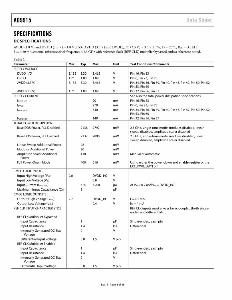
SPECIFICATIONS DC SPECIFICATIONS AVDD (1.8 V) and DVDD (1.8 V) = 1.8 V ± 5%, AVDD (3.3 V) and DVDD_I/O (3.3 V) = 3.3 V ± 5%, TA = 25°C, RSET = 3.3 kΩ, IOUT = 20 mA, external reference clock frequency = 2.5 GHz with reference clock (REF CLK) multiplier bypassed, unless otherwise noted.
Table 1. Parameter Min Typ Max Unit Test Conditions/Comments
SUPPLY VOLTAGE DVDD_I/O 3.135 3.30 3.465 V Pin 16, Pin 83 DVDD 1.71 1.80 1.89 V Pin 6, Pin 23, Pin 73 AVDD (3.3 V) 3.135 3.30 3.465 V Pin 34, Pin 36, Pin 39, Pin 40, Pin 43, Pin 47, Pin 50, Pin 52,
Pin 53, Pin 60 AVDD (1.8 V) 1.71 1.80 1.89 V Pin 32, Pin 56, Pin 57
SUPPLY CURRENT See also the total power dissipation specifications IDVDD_I/O 20 mA Pin 16, Pin 83 IDVDD 270 mA Pin 6, Pin 23, Pin 73 IAVDD(3.3V) 640 mA Pin 34, Pin 36, Pin 39, Pin 40, Pin 43, Pin 47, Pin 50, Pin 52,
Pin 53, Pin 60 IAVDD(1.8V) 148 mA Pin 32, Pin 56, Pin 57
TOTAL POWER DISSIPATION Base DDS Power, PLL Disabled 2138 2797 mW 2.5 GHz, single-tone mode, modules disabled, linear
sweep disabled, amplitude scaler disabled Base DDS Power, PLL Enabled 2237 2890 mW 2.5 GHz, single-tone mode, modules disabled, linear
sweep disabled, amplitude scaler disabled Linear Sweep Additional Power 28 mW Modulus Additional Power 20 mW Amplitude Scaler Additional
Power 138 mW Manual or automatic
Full Power-Down Mode 400 616 mW Using either the power-down and enable register or the EXT_PWR_DWN pin
CMOS LOGIC INPUTS Input High Voltage (VIH) 2.0 DVDD_I/O V Input Low Voltage (VIL) 0.8 V Input Current (IINH, IINL) ±60 ±200 µA At VIN = 0 V and VIN = DVDD_I/O Maximum Input Capacitance (CIN) 3 pF
CMOS LOGIC OUTPUTS Output High Voltage (VOH) 2.7 DVDD_I/O V IOH = 1 mA Output Low Voltage (VOL) 0.4 V IOL = 1 mA
REF CLK INPUT CHARACTERISTICS REF CLK inputs must always be ac-coupled (both single-ended and differential)
REF CLK Multiplier Bypassed Input Capacitance 1 pF Single-ended, each pin Input Resistance 1.4 kΩ Differential Internally Generated DC Bias
Voltage 2 V
Differential Input Voltage 0.8 1.5 V p-p REF CLK Multiplier Enabled
Input Capacitance 1 pF Single-ended, each pin Input Resistance 1.4 kΩ Differential Internally Generated DC Bias
Voltage 2 V
Differential Input Voltage 0.8 1.5 V p-p

Data Sheet AD9915
Rev. E | Page 5 of 48
AC SPECIFICATIONS AVDD (1.8 V) and DVDD (1.8 V) = 1.8 V ± 5%, AVDD3 (3.3 V) and DVDD_I/O (3.3 V) = 3.3 V ± 5%, TA = 25°C, RSET = 3.3 kΩ, IOUT = 20 mA, external reference clock frequency = 2.5 GHz with reference clock (REF CLK) multiplier bypassed, unless otherwise noted.
Table 2. Parameter Min Typ Max Unit Test Conditions/Comments
REF CLK INPUT Input frequency range REF CLK Multiplier Bypassed
Input Frequency Range 500 2500 MHz Maximum fOUT is 0.4 × fSYSCLK Duty Cycle 45 55 % Minimum Differential Input Level 632 mV p-p Equivalent to 316 mV swing on each leg
System Clock (SYSCLK) PLL Enabled VCO Frequency Range 2400 2500 MHz VCO Gain (KV) 60 MHz/V Maximum PFD Rate 125 MHz
CLOCK DRIVERS SYNC_CLK Output Driver
Frequency Range 156 MHz Duty Cycle 45 50 55 % Rise Time/Fall Time (20% to 80%) 650 ps
SYNC_OUT Output Driver 10 pF load Frequency Range 6.5 MHz Duty Cycle 33 66 % CFR2 register, Bit 9 = 1 Rise Time (20% to 80%) 1350 ps 10 pF load Fall Time (20% to 80%) 1670 ps 10 pF load
DAC OUTPUT CHARACTERISTICS Output Frequency Range (1st Nyquist
Zone) 0 1250 MHz
Output Resistance 50 Ω Single-ended (each pin internally terminated to AVDD (3.3 V))
Output Capacitance 1 pF Full-Scale Output Current 20.48 mA Range depends on DAC RSET resistor Gain Error −10 +10 % FS Output Offset 0.6 μA Voltage Compliance Range AVDD −
0.50 AVDD +
0.50 V
Wideband SFDR See the Typical Performance Characteristics section
122.5 MHz Output −67 dBc 0 MHz to 1250 MHz 305.3 MHz Output −66 dBc 0 MHz to 1250 MHz 497.5 MHz Output −59 dBc 0 MHz to 1250 MHz 978.2 MHz Output −60 dBc 0 MHz to 1250 MHz
Narrow-Band SFDR See the Typical Performance Characteristics section
122.5 MHz Output −95 dBc ±500 kHz 305.3 MHz Output −95 dBc ±500 kHz 497.5 MHz Output −95 dBc ±500 kHz 978.2 MHz Output −92 dBc ±500 kHz
DIGITAL TIMING SPECIFICATIONS Time Required to Enter Power-Down 45 ns Power-down mode loses DAC/PLL calibration
settings Time Required to Leave Power-Down 250 ns Must recalibrate DAC/PLL Minimum Master Reset time 24 SYSCLK cycles Maximum DAC Calibration Time (tCAL) 188 µs See the DAC Calibration Output section for
formula; Bit 6 in Register 0x1B = 0 Maximum PLL Calibration Time (tREF_CLK) 16 ms PFD rate = 25 MHz 8 ms PFD rate = 50 MHz Maximum Profile Toggle Rate 2 SYNC_CLK period
AD9915 Data Sheet
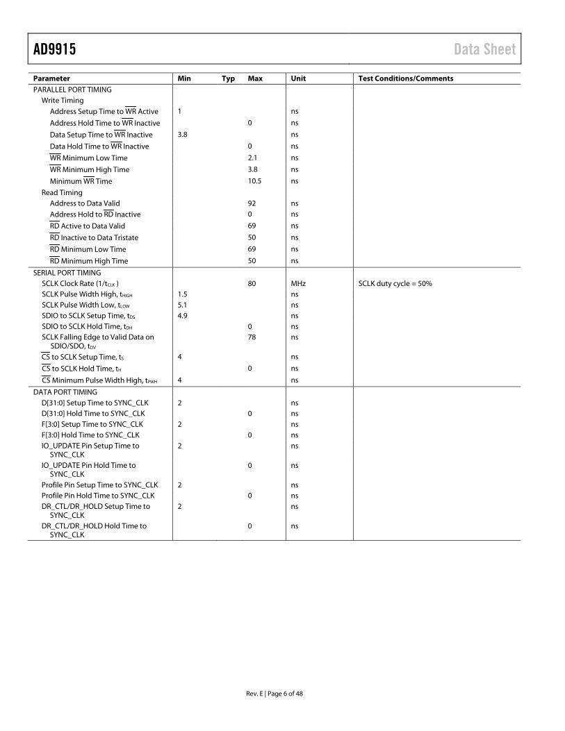
Rev. E | Page 6 of 48
Parameter Min Typ Max Unit Test Conditions/Comments PARALLEL PORT TIMING
Write Timing Address Setup Time to WR Active 1 ns
Address Hold Time to WR Inactive 0 ns
Data Setup Time to WR Inactive 3.8 ns
Data Hold Time to WR Inactive 0 ns
WR Minimum Low Time 2.1 ns
WR Minimum High Time 3.8 ns
Minimum WR Time 10.5 ns
Read Timing Address to Data Valid 92 ns Address Hold to RD Inactive 0 ns
RD Active to Data Valid 69 ns
RD Inactive to Data Tristate 50 ns
RD Minimum Low Time 69 ns
RD Minimum High Time 50 ns
SERIAL PORT TIMING SCLK Clock Rate (1/tCLK ) 80 MHz SCLK duty cycle = 50% SCLK Pulse Width High, tHIGH 1.5 ns SCLK Pulse Width Low, tLOW 5.1 ns SDIO to SCLK Setup Time, tDS 4.9 ns SDIO to SCLK Hold Time, tDH 0 ns SCLK Falling Edge to Valid Data on
SDIO/SDO, tDV 78 ns
CS to SCLK Setup Time, tS 4 ns
CS to SCLK Hold Time, tH 0 ns
CS Minimum Pulse Width High, tPWH 4 ns
DATA PORT TIMING D[31:0] Setup Time to SYNC_CLK 2 ns D[31:0] Hold Time to SYNC_CLK 0 ns F[3:0] Setup Time to SYNC_CLK 2 ns F[3:0] Hold Time to SYNC_CLK 0 ns IO_UPDATE Pin Setup Time to
SYNC_CLK 2 ns
IO_UPDATE Pin Hold Time to SYNC_CLK
0 ns
Profile Pin Setup Time to SYNC_CLK 2 ns Profile Pin Hold Time to SYNC_CLK 0 ns DR_CTL/DR_HOLD Setup Time to
SYNC_CLK 2 ns
DR_CTL/DR_HOLD Hold Time to SYNC_CLK
0 ns

Data Sheet AD9915
Rev. E | Page 7 of 48
Parameter Min Typ Max Unit Test Conditions/Comments DATA LATENCY (PIPELINE DELAY) SYSCLK cycles = fS = system clock frequency
in GHz Single Tone Mode or Profile Mode
(Matched Latency Disabled)
Frequency 222 SYSCLK cycles OSK disabled 238 SYSCLK cycles OSK enabled Phase 206 SYSCLK cycles OSK disabled 222 SYSCLK cycles OSK enabled Amplitude 78 SYSCLK cycles OSK enabled
Single Tone Mode or Profile Mode (Matched Latency Enabled)
Frequency 222 SYSCLK cycles OSK disabled 238 SYSCLK cycles OSK enabled Phase 222 SYSCLK cycles OSK disabled 238 SYSCLK cycles OSK enabled Amplitude 238 SYSCLK cycles OSK enabled
Modulation Mode with 32-Bit Parallel Port (Match Latency Disabled)
Frequency 222 SYSCLK cycles OSK disabled 238 SYSCLK cycles OSK enabled Phase 206 SYSCLK cycles OSK disabled 222 SYSCLK cycles OSK enabled Amplitude 78 SYSCLK cycles OSK enabled
Modulation Mode with 32-Bit Parallel Port (Match Latency Enabled)
Frequency 222 SYSCLK cycles OSK disabled 238 SYSCLK cycles OSK enabled Phase 222 SYSCLK cycles OSK disabled 238 SYSCLK cycles OSK enabled Amplitude 238 SYSCLK cycles OSK enabled
Sweep Mode (Match Latency Disabled) Frequency 238 SYSCLK cycles OSK disabled 254 SYSCLK cycles OSK enabled Phase 222 SYSCLK cycles OSK disabled 238 SYSCLK cycles OSK enabled Amplitude 94 SYSCLK cycles OSK enabled
Sweep Mode (Match Latency Enabled) Frequency 238 SYSCLK cycles OSK disabled 254 SYSCLK cycles OSK enabled Phase 238 SYSCLK cycles OSK disabled 254 SYSCLK cycles OSK enabled Amplitude 254 SYSCLK cycles OSK enabled

AD9915 Data Sheet
Rev. E | Page 8 of 48
ABSOLUTE MAXIMUM RATINGS Table 3. Parameter Rating AVDD (1.8 V), DVDD (1.8 V) Supplies 2 V AVDD (3.3 V), DVDD_I/O (3.3 V) Supplies 4 V Digital Input Voltage −0.7 V to +4 V Digital Output Current 5 mA Storage Temperature Range −65°C to +150°C Operating Temperature Range −40°C to +85°C Maximum Junction Temperature 150°C Lead Temperature (10 sec Soldering) 300°C
Stresses at or above those listed under Absolute Maximum Ratings may cause permanent damage to the product. This is a stress rating only; functional operation of the product at these or any other conditions above those indicated in the operational section of this specification is not implied. Operation beyond the maximum operating conditions for extended periods may affect product reliability.
THERMAL PERFORMANCE
Table 4. Symbol Description Value1 Unit
θJA Junction-to-ambient thermal resistance (still air) per JEDEC JESD51-2
24.1 °C/W
θJMA Junction-to-ambient thermal resistance (1.0 m/sec airflow) per JEDEC JESD51-6
21.3 °C/W
θJMA Junction-to-ambient thermal resistance (2.0 m/sec air flow) per JEDEC JESD51-6
20.0 °C/W
θJB Junction-to-board thermal resistance (still air) per JEDEC JESD51-8
13.3 °C/W
ΨJB Junction-to-board characterization parameter (still air) per JEDEC JESD51-6
12.8 °C/W
θJC Junction-to-case thermal resistance 2.21 °C/W
ΨJT Junction-to-top-of-package characterization parameter (still air) per JEDEC JESD51-2
0.23 °C/W
1 Results are from simulations. PCB is JEDEC multilayer. Thermal performance
for actual applications requires careful inspection of the conditions in the application to determine if they are similar to those assumed in these calculations.
ESD CAUTION

Data Sheet AD9915
Rev. E | Page 9 of 48
PIN CONFIGURATION AND FUNCTION DESCRIPTIONS
Figure 3. Pin Configuration
Table 5. Pin Function Descriptions Pin No. Mnemonic I/O1 Description 1, 2, 13 to 15, 68 to 72, 75 to 81, 87, 88
D5 to D7, D16 to D31, D27 to D31
I/O Parallel Port Pins. The 32-bit parallel port offers the option for serial or parallel programming of the internal registers. In addition, the parallel port can be configured to provide direct FSK, PSK, or ASK (or combinations thereof ) modulation data. The 32-bit parallel port configuration is set by the state of the four function pins (F0 to F3).
3 D15/A7 I/O Parallel Port Pin/Address Line. The state of the F0 to F3 function pins determines if this pin acts as a line for direct FSK, PSK, or ASK data or as an address line for programming the internal registers.
4 D14/A6 I/O Parallel Port Pin/Address Line. The state of the F0 to F3 function pins determines if this pin acts as a line for direct FSK, PSK, or ASK data or as an address line for programming the internal registers.
5 D13/A5 I/O Parallel Port Pin/Address Line. The state of the F0 to F3 function pins determines if this pin acts as a line for direct FSK, PSK, or ASK data or as an address line for programming the internal registers.
8 D12/A4 I/O Parallel Port Pin/Address Line. The state of the F0 to F3 function pins determines if this pin acts as a line for direct FSK, PSK, or ASK data or as an address line for programming the internal registers.
9 D11/A3 I/O Parallel Port Pin/Address Line. The state of the F0 to F3 function pins determines if this pin acts as a line for direct FSK, PSK, or ASK data or as an address line for programming the internal registers.
10 D10/A2 I/O Parallel Port Pin/Address Line. Multipurpose pin depending on the state of the function pins (F0 to F3). The state of the F0 to F3 function pins determines if this pin acts as a line for direct FSK, PSK, or ASK data or as an address line for programming the internal registers.
11 D9/A1 I/O Parallel Port Pin/Address Line. Multipurpose pin depending on the state of the function pins (F0 to F3). The state of the F0 to F3 function pins determines if this pin acts as a line for direct FSK, PSK, or ASK data or as an address line for programming the internal registers.
123456789
10111213141516
D17D16
D15/A7D14/A6D13/A5
DVDD (1.8V)DGND
D12/A4D11/A3D10/A2
D9/A1D8/A0
D7D6D5
DVDD_I/O (3.3V)17DGND18D4/SYNCIO19D3/SDO20D2/SDIO/WR
23 24 25 26 27 28 29 30 31 32 33 34 36 37
DVD
D (1
.8V)
DG
ND
PS0
PS1
PS2 F0 F1 F2 F3
AVD
D (1
.8V)
AG
ND
AVD
D (3
.3V)
35A
GN
DAV
DD
(3.3
V)A
GN
D38
AG
ND
39AV
DD
(3.3
V)40
AVD
D (3
.3V)
41A
OU
T
5857565554535251504948474645
LOOP_FILTER59 REF60 AVDD (3.3V)61 SYNC_OUT62 SYNC_IN63 DRCTL64 DRHOLD65 DROVER66 OSK
AVDD (1.8V)AVDD (1.8V)REF CLKREF CLKAVDD (3.3V)AVDD (3.3V)AGNDAVDD (3.3V)AGNDDAC_RSETAVDD (3.3V)AGNDDAC_BP
78 77 76 75 74 73 72 71 70 69 68 67
D23
79D
2280
D21
81D
2082
SYN
C_C
LK83
DVD
D_I
/O (3
.3V)
84D
GN
D85
MA
STER
_RES
ET86
I/O_U
PDAT
E87
D19
88D
18
D24
D25
D26
DG
ND
DVD
D (1
.8V)
D27
D28
D29
D30
D31
EXT_
PWR
_DW
NNOTES1. THE EPAD MUST BE SOLDERED TO GROUND.
21D1/SCLK/RD22D0/CS/PWD
42A
OU
T43
AVD
D (3
.3V)
44A
GN
D
AD9915TOP VIEW
(Not to Scale)
1083
7-00
3

AD9915 Data Sheet
Rev. E | Page 10 of 48
Pin No. Mnemonic I/O1 Description 12 D8/A0 I/O Parallel Port Pin/Address Line. The state of the F0 to F3 function pins determines if this pin
acts as a line for direct FSK, PSK, or ASK data or as an address line for programming the internal registers.
18 D4/SYNCIO I Parallel Port Pin/Serial Port Synchronization Pin. This pin is D4 for direct FSK, PSK, or ASK data. If serial mode is invoked via F0 to F3, this pin resets the serial port.
19 D3/SDO I/O Parallel Port Pin/Serial Data Output This pin is D3 for direct FSK, PSK, or ASK data. If serial mode is invoked via F0 to F3, this pin is used for readback mode for serial operation.
20 D2/SDIO/WR I/O Parallel Port Pin/Serial Data Input and Output/Write Input. This pin is D2 for direct FSK, PSK, or ASK data. If serial mode is invoked via F0 to F3, this pin is used for the SDIO for serial operation. If parallel mode is enabled, this pin writes to change the values of the internal registers.
21 D1/SCLK/RD I Parallel Port Pin/Serial Clock/Read Input. This pin is D1 for direct FSK, PSK, or ASK data. If serial mode is invoked via F0 to F3, this pin is used for SCLK for serial operation. If parallel mode is enabled, this pin reads back the value of the internal registers.
22 D0/CS/PWD I Parallel Port Pin/Chip Select/Parallel Width. This pin is D0 for direct FSK, PSK, or ASK data. If serial mode is invoked via F0 to F3, this pin is used for the chip select for serial operation. If parallel mode is enabled, this pin sets either 8-bit data or 16-bit data.
6, 23, 73 DVDD (1.8V) I Digital Core Supplies (1.8 V). 7, 17, 24, 74, 84 DGND I Digital Ground. 16, 83 DVDD_I/O (3.3V) I Digital Input/Output Supplies (3.3 V). 32, 56, 57 AVDD (1.8V) I Analog Core Supplies (1.8 V). 33, 35, 37, 38, 44, 46, 49, 51
AGND I Analog Ground.
34, 36, 39, 40, 43, 47, 50, 52, 53, 60
AVDD (3.3V) I Analog DAC Supplies (3.3 V).
25, 26, 27 PS0 to PS2 I Profile Select Pins. Digital inputs (active high). Use these pins to select one of eight phase/frequency profiles for the DDS. Changing the state of one of these pins transfers the current contents of all input/output buffers to the corresponding registers. State changes must be set up on the SYNC_CLK pin (Pin 82).
28, 29, 30, 31 F0 to F3 I Function Pins. Digital inputs. The state of these pins determines if a serial or parallel interface is used. In addition, the function pins determine how the 32-bit parallel data-word is partitioned for FSK, PSK, or ASK modulation mode.
41 AOUT O DAC Complementary Output Source. Analog output (voltage mode). Internally connected through a 50 Ω resistor to AVDD (3.3 V).
42 AOUT O DAC Output Source. Analog output (voltage mode). Internally connected through a 50 Ω resistor to AVDD (3.3 V).
45 DAC_BP I DAC Bypass Pin. Provides access to the common control node of the DAC current sources. Connecting a capacitor between this pin and ground can improve noise performance at the DAC output.
48 DAC_RSET O Analog Reference. This pin programs the DAC output full-scale reference current. Connect a 3.3 kΩ resistor to AGND.
54 REF_CLK I Complementary Reference Clock Input. Analog input.
55 REF_CLK I Reference Clock Input. Analog input. 58 LOOP_FILTER O External PLL Loop Filter Node. 59 REF O Local PLL Reference Supply. Typically at 2.05 V. 61 SYNC_OUT O Digital Synchronization Output. The pin synchronizes multiple chips. 62 SYNC_IN I Digital Synchronization Input. The pin synchronizes multiple chips. 63 DRCTL I Ramp Control. Digital input (active high). This pin controls the sweep direction (up/down). 64 DRHOLD I Ramp Hold. Digital input (active high). Pauses the sweep when active. 65 DROVER O Ramp Over. Digital output (active high). This pin switches to Logic 1 when the digital ramp
generator reaches the programmed upper or lower limit. 66 OSK I Output Shift Keying. Digital input (active high). When the OSK features are placed in either
manual or automatic mode, this pin controls the OSK function. In manual mode, it toggles the multiplier between 0 (low) and the programmed amplitude scale factor (high). In automatic mode, a low sweeps the amplitude down to zero and a high sweeps the amplitude up to the amplitude scale factor.

Data Sheet AD9915
Rev. E | Page 11 of 48
Pin No. Mnemonic I/O1 Description 67 EXT_PWR_DWN I External Power-Down. Digital input (active high). A high level on this pin initiates the
currently programmed power-down mode. 82 SYNC_CLK O Clock Output. Digital output. Many of the digital inputs on the chip, such as I/O_UPDATE,
PS[2:0], and the parallel data port (D0 to D31), must be set up on the rising edge of this signal.
85 MASTER_RESET I Master Reset. Digital input (active high). Clears all memory elements and sets registers to default values.
86 I/O_UPDATE I Input/Output Update. Digital input (active high). A high on this pin transfers the contents of the input/output buffers to the corresponding internal registers.
EPAD Exposed Pad. The EPAD must be soldered to ground. 1 I = input, O = output.

AD9915 Data Sheet
Rev. E | Page 12 of 48
TYPICAL PERFORMANCE CHARACTERISTICS Nominal supply voltage; DAC RSET = 3.3 kΩ, TA = 25°C, unless otherwise noted.
Figure 4. Wideband SFDR at 122.5 MHz
SYSCLK = 2.5 GHz (SYSCLK PLL Bypassed)
Figure 5. Wideband SFDR at 305.3 MHz
SYSCLK = 2.5 GHz (SYSCLK PLL Bypassed)
Figure 6. Wideband SFDR at 497.5 MHz,
SYSCLK = 3.5 GHz (SYSCLK PLL Bypassed)
Figure 7. Narrow-Band SFDR at 122.5 MHz,
SYSCLK = 2.5 GHz (SYSCLK PLL Bypassed)
Figure 8. Narrow-Band SFDR at 305.3 MHz,
SYSCLK = 2.5 GHz (SYSCLK PLL Bypassed)
Figure 9. Narrow-Band SFDR at 497.5 MHz, SYSCLK = 2.5 GHz (SYSCLK PLL Bypassed)
START 0Hz–100
–90
–80
–70
–60
–50
–40
–30
–20
–10
0
125MHz/DIV STOP 1.25GHz
SFD
R (d
Bc)
1083
7-00
4
START 0Hz–100
–90
–80
–70
–60
–50
–40
–30
–20
–10
0
125MHz/DIV STOP 1.25GHz
SFD
R (d
Bc)
1083
7-00
5
START 0Hz–100
–90
–80
–70
–60
–50
–40
–30
–20
–10
0
125MHz/DIV STOP 1.25GHz
SFD
R (d
Bc)
1083
7-00
6
CENTER 122.499MHz–100
–90
–80
–70
–60
–50
–40
–30
–20
–10
0
50kHz/DIV SPAN 500kHz
SFD
R (d
Bc)
1083
7-00
7
CENTER 305.357MHz–100
–90
–80
–70
–60
–50
–40
–30
–20
–10
0
50kHz/DIV SPAN 500kHz
SFD
R (d
Bc)
1083
7-00
8
CENTER 497.499MHz–100
–90
–80
–70
–60
–50
–40
–30
–20
–10
0
50kHz/DIV SPAN 500kHz
SFD
R (d
Bc)
1083
7-00
9

Data Sheet AD9915
Rev. E | Page 13 of 48
Figure 10. Wideband SFDR at 978.2 MHz, SYSCLK = 2.5 GHz (SYSCLK PLL Bypassed)
Figure 11. Wideband SFDR vs. Normalized fOUT
SYSCLK = 2.5 GHz
Figure 12. Wideband SFDR vs. Normalized fOUT,
SYSCLK = 2.5 GHz to 2.5 GHz
Figure 13. Narrow-Band SFDR at 978.2 MHz,
SYSCLK = 2.5 GHz (SYSCLK PLL Bypassed)
Figure 14. Absolute Phase Noise of REF CLK Source Driving AD9915 Rohde & Schwarz SMA100 Signal Generator at 2.5 GHz Buffered by Series
ADCLK925
Figure 15. Absolute Phase Noise Curves of DDS Output at 2.5 GHz Operation
–100
–90
–80
–70
–60
–50
–40
–30
–20
–10
0
SFD
R (d
Bc)
START 0Hz 125MHz/DIV STOP 1.25GHz 1083
7-01
00
–800 0.05 0.10 0.15 0.400.350.300.250.20
SFD
R (d
Bc)
fC/fS
–70
–60
–50
–40
–30
–20
–10
1083
7-01
1
0
–800 0.05 0.10 0.15 0.400.350.300.250.20
SFD
R (d
Bc)
fC/fS
–70
–60
–50
–40
–30
–20
–10
1083
7-01
2
SYSCLK = 1.5GHzSYSCLK = 1.6GHzSYSCLK = 1.7GHzSYSCLK = 1.8GHzSYSCLK = 1.9GHzSYSCLK = 2.0GHzSYSCLK = 2.1GHzSYSCLK = 2.2GHzSYSCLK = 2.3GHzSYSCLK = 2.4GHzSYSCLK = 2.5GHz
CENTER 978.214MHz–100
–90
–80
–70
–60
–50
–40
–30
–20
–10
0
50kHz/DIV SPAN 500kHz
SFD
R (d
Bc)
1083
7-01
3
10 100 1k 10k 100k 1M 10M 100MFREQUENCY OFFSET (Hz)
–70
–90
–80
–100
–110
–120
–130
–140
–150
–160
–170
PHA
SE N
OIS
E (d
Bc/
Hz)
SMA ANDADCLK925
1083
7-01
4
SMA
10 100 1k 10k 100k 1M 10M 100MFREQUENCY OFFSET (Hz)
–70
–90
–80
–100
–110
–120
–130
–140
–150
–160
–170
PHA
SE N
OIS
E (d
Bc/
Hz)
978MHz10
837-
015
123MHz
305MHz
497MHz
AD9915 Data Sheet
Rev. E | Page 14 of 48
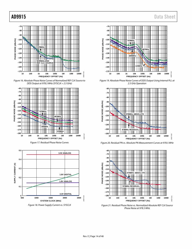
Figure 16. Absolute Phase Noise Curves of Normalized REF CLK Source to
DDS Output at 978.5 MHz (SYSCLK = 2.5 GHz)
Figure 17. Residual Phase Noise Curves
Figure 18. Power Supply Current vs. SYSCLK
Figure 19. Absolute Phase Noise Curves of DDS Output Using Internal PLL at
2.5 GHz Operation
Figure 20. Residual PN vs. Absolute PN Measurement Curves at 978.5 MHz
Figure 21. Residual Phase Noise vs. Normalized Absolute REF CLK Source Phase Noise at 978.5 MHz
1083
7-01
6
10 100 1k 10k 100k 1M 10M 100MFREQUENCY OFFSET (Hz)
–70
–90
–80
–100
–110
–120
–130
–140
–150
–160
–170
PHA
SE N
OIS
E (d
Bc/
Hz)
978MHz
NORMALIZEDREF CLK SOURCE
1083
7-01
7
–60
–90
–80
–70
–100
–110
–120
–130
–140
–150
–160
–170
–18010 100 1k 10k 100k 1M 10M 100M
FREQUENCY OFFSET (Hz)
PHA
SE N
OIS
E (d
Bc/
Hz)
978MHz
123MHz
497MHz
305MHz
0.5
0.4
0.3
0.2
0.1
0500 1000 250020001500
SUPP
LY C
UR
REN
T (A
)
SYSTEM CLOCK (MHz) 1083
7-01
8
3.3V ANALOG
3.3V DIGITAL
1.8V ANALOG
1.8V DIGITAL
10 100 1k 10k 100k 1M 10M 100MFREQUENCY OFFSET (Hz)
–70
–90
–80
–100
–110
–120
–130
–140
–150
–160
–170
PHA
SE N
OIS
E (d
Bc/
Hz) 978MHz
305MHz
123MHz
497MHz
1083
7-01
9
10 100 1k 10k 100k 1M 10M 100MFREQUENCY OFFSET (Hz)
PHA
SE N
OIS
E (d
Bc/
Hz)
–60
–90
–80
–70
–100
–110
–120
–130
–140
–150
–160
1083
7-02
0
978MHz RESIDUAL
978MHz ABSOLUTE
–60
–90
–80
–70
–100
–110
–120
–130
–140
–150
–160
–170
–18010 100 1k 10k 100k 1M 10M 100M
FREQUENCY OFFSET (Hz)
PHA
SE N
OIS
E (d
Bc/
Hz)
978MHz ABSOLUTE
978MHz RESIDUAL
1083
7-02
1

Data Sheet AD9915
Rev. E | Page 15 of 48
Figure 22. SYNC_OUT (fSYSCLK/384)
Figure 23. DAC Calibration Time vs. SYSCLK Rate. See the DAC Calibration
Output section for formula.
Figure 24. Measured Rising Linear Frequency Sweep
Figure 25. Measured Falling Linear Frequency Sweep
CH2 1.0V Ω M20.00ms 5.0GS/s IT 40.0ps/ptA CH2 1.64V
2
1083
7-02
2
1.0
0.9
0.1
0.2
0.3
0.4
0.5
0.6
0.7
0.8
0500 2500
TIM
E (m
s)
SYSTEM CLOCK RATE (MHz)1000 1500 2000
1083
7-02
3
930
870
880
890
900
910
920
–6 –2–4 6420
FREQ
UEN
CY
(MH
z)
TIME (ms) 1083
7-02
4
930
870
880
890
900
910
920
–6 –2–4 6420
FREQ
UEN
CY
(MH
z)
TIME (ms) 1083
7-02
5

AD9915 Data Sheet
Rev. E | Page 16 of 48
EQUIVALENT CIRCUITS
Figure 26. DAC Output
Figure 27. REF CLK input
Figure 28. CMOS Input
Figure 29. CMOS Output
1083
7-04
4
SWITCHCONTROL
CODE
AGND
AVDD (3.3V)
CURRENTSWITCHARRAY
CURRENTSWITCHARRAY
AOUT AOUT
INTERNAL50Ω
INTERNAL50Ω
IFS/2 + ICODE IFS/2 – ICODE
IFS
414210
837-
048
AVDD (3.3V)
REF_CLK REF_CLK
DVDD (3.3V)
1083
7-04
5
DVDD (3.3V)
1083
7-04
3

Data Sheet AD9915
Rev. E | Page 17 of 48
THEORY OF OPERATION The AD9915 has five modes of operation. • Single tone • Profile modulation • Digital ramp modulation (linear sweep) • Parallel data port modulation • Programmable modulus mode
The modes define the data source that supplies the DDS with the signal control parameters: frequency, phase, or amplitude. The partitioning of the data into different combinations of frequency, phase, and amplitude is established based on the mode and/or specific control bits and function pins.
Although the various modes are described independently, they can be enabled simultaneously. This provides an unprecedented level of flexibility for generating complex modulation schemes. However, to avoid multiple data sources from driving the same DDS signal control parameter, the device has a built in priority protocol.
In single tone mode, the DDS signal control parameters come directly from the profile programming registers. In digital ramp modulation mode, the DDS signal control parameters are delivered by a digital ramp generator. In parallel data port modulation mode, the DDS signal control parameters are driven directly into the parallel port.
The various modulation modes generally operate on only one of the DDS signal control parameters (two in the case of the polar modulation format via the parallel data port). The unmodulated DDS signal control parameters are stored in programming registers and automatically routed to the DDS based on the selected mode.
A separate output shift keying (OSK) function is also available. This function employs a separate digital linear ramp generator that affects only the amplitude parameter of the DDS. The OSK function has priority over the other data sources that can drive the DDS amplitude parameter. As such, no other data source can drive the DDS amplitude when the OSK function is enabled.
SINGLE TONE MODE In single tone mode, the DDS signal control parameters are supplied directly from the profile programming registers. A profile is an independent register that contains the DDS signal control parameters. Eight profile registers are available. Note that the profile pins must select the desired register.
PROFILE MODULATION MODE Each profile is independently accessible. For FSK, PSK, or ASK modulation, use the three external profile pins (PS[2:0]) to select the desired profile. A change in the state of the profile pins with the next rising edge on SYNC_CLK updates the DDS with the parameters specified by the selected profile.
Therefore, the profile change must meet the setup and hold times to the SYNC_CLK rising edge. Note that amplitude control must also be enabled using the OSK enable bit in the CFR1 register (0x00[8]).
DIGITAL RAMP MODULATION MODE In digital ramp modulation mode, the modulated DDS signal control parameter is supplied directly from the digital ramp generator (DRG). The ramp generation parameters are controlled through the serial or parallel input/output port.
The ramp generation parameters allow the user to control both the rising and falling slopes of the ramp. The upper and lower boundaries of the ramp, the step size and step rate of the rising portion of the ramp, and the step size and step rate of the falling portion of the ramp are all programmable.
The ramp is digitally generated with 32-bit output resolution. The 32-bit output of the DRG can be programmed to affect frequency, phase, or amplitude. When programmed for frequency, all 32 bits are used. However, when programmed for phase or amplitude, only the 16 MSBs or 12 MSBs, respectively, are used.
The ramp direction (rising or falling) is externally controlled by the DRCTL pin. An additional pin (DRHOLD) allows the user to suspend the ramp generator in the present state. Note that amplitude control must also be enabled using the OSK enable bit in Register CFR1.
PARALLEL DATA PORT MODULATION MODE In parallel data port modulation mode, the modulated DDS signal control parameter(s) are supplied directly from the 32-bit parallel data port. The function pins define how the 32-bit data-word is applied to the DDS signal control parameters. Format-ting of the 32-bit data-word is unsigned binary, regardless of the destination.
Parallel Data Clock (SYNC_CLK)
The AD9915 generates a clock signal on the SYNC_CLK pin that runs at 1/16 of the DAC sample rate (the sample rate of the parallel data port). SYNC_CLK serves as a data clock for the parallel port.
PROGRAMMABLE MODULUS MODE In programmable modulus mode, the DRG is used as an auxiliary accumulator to alter the frequency equation of the DDS core, making it possible to implement fractions that are not restricted to a power of 2 in the denominator. A standard DDS is restricted to powers of 2 as a denominator because the phase accumulator is a set of bits as wide as the frequency tuning word (FTW).
When in programmable modulus mode, however, the frequency equation is:
f0 = (fS)(FTW + A/B)/232
where f0/fS < ½, 0 ≤ FTW < 231, 2 ≤ B ≤ 232 – 1, and A < B.

AD9915 Data Sheet
Rev. E | Page 18 of 48
This equation implies a modulus of B × 232 (rather than 232, in the case of a standard DDS). Furthermore, because B is program-mable, the result is a DDS with a programmable modulus.
When in programmable modulus mode, the 32-bit auxiliary accumulator operates in a way that allows it to roll over at a value other than the full capacity of 232. That is, it operates with a modified modulus based on the programmable value of B. With each roll over of the auxiliary accumulator, a value of 1 LSB adds to the current accumulated value of the 32-bit phase accumulator. This behavior changes the modulus of the phase accumulator to B × 232 (instead of 232), allowing it to synthesize the desired f0.
To determine the programmable modulus mode register values for FTW, A, and B, the user must first define f0/fS as a ratio of relatively prime integers, M/N. That is, having converted f0 and fS to integers, M and N, reduce the fraction, M/N, to the lowest terms. Then, divide M × 232 by N. The integer part of this division operation is the value of FTW (Register 0x04[31:0]). The remainder, Y, of this division operation is
Y = (232 × M) – (FTW × N)
The value of Y facilitates the determination of A and B by taking the fraction, Y/N, and reducing it to the lowest terms. Then, the numerator of the reduced fraction is A (Register 0x06[31:0]) and the denominator is the B (Register 0x05[31:0]).
For example, synthesizing precisely 300 MHz with a 1 GHz system clock is not possible with a standard DDS. It is possible, however, using programmable modulus as follows.
First, express f0/fS as a ratio of integers:
300,000,000/1,000,000,000
Reducing this fraction to lowest terms yields 3/10; therefore, M = 3 and N = 10. FTW is the integer part of (M × 232)/N, or (3 × 232)/10, which is 1,288,490,188 (0x4CCCCCCC in 32-bit hexadecimal notation). The remainder, Y, of (3 × 232)/10, is (232 × 3) − (1,288,490,188 × 10), which is 8. Therefore, Y/N is 8/10, which reduces to 4/5. Therefore, A = 4 and B = 5 (0x00000004 and 0x00000005 in 32-bit hexadecimal notation, respectively). Programming the AD9915 with these values of FTW, A, and B results in an output frequency that is exactly 3/10 of the system clock frequency.
MODE PRIORITY The ability to activate each mode independently makes it possible to have multiple data sources attempting to drive the same DDS signal control parameter (frequency, phase, and amplitude). To avoid contention, the AD9915 has a built in priority system. Table 6 summarizes the priority for each of the DDS modes. The data source column in Table 6 lists data sources for a particular DDS signal control parameter in descending order of precedence. For example, if the profile mode enable bit and the parallel data port enable bit (0x01[23:22]) are set to Logic 1 and both are programmed to source the frequency tuning word to DDS output, the profile modulation mode has priority over the parallel data port modulation mode.
Table 6. Data Source Priority
Priority DDS Signal Control Parameters
Data Source Conditions Highest
Priority Programmable modulus
If programmable modulus mode is used to output frequency only, no other data source can control the output frequency in this mode. Note that the DRG is used in conjunction with programmable modulus mode; therefore, the DRG cannot be used to sweep phase or amplitude in programmable modulus mode. If output phase offset control is desired, enable profile mode and use the profile registers and profile pins accordingly to control output phase adjustment. If output amplitude control is desired, enable profile mode and use the profile registers and profile pins accordingly to control output amplitude adjustment. Note that the OSK enable bit must be set to control the output amplitude.
DRG The digital ramp modulation mode is the next highest priority mode. If the DRG is enabled to sweep output frequency, phase, or amplitude, the two parameters not being swept can be controlled independently via the profile mode.
Profiles The profile modulation mode is the next highest priority mode. Profile mode can control all three parameters independently, if desired.
Lowest Priority
Parallel port Parallel data port modulation has the lowest priority but the most flexibility as far as changing any parameter at the high rate. See the Programming and Function Pins section.

Data Sheet AD9915
Rev. E | Page 19 of 48
FUNCTIONAL BLOCK DETAIL DDS CORE The direct digital synthesizer (DDS) block generates a reference signal (sine or cosine based on Register 0x00, Bit 16, the enable sine output bit). The parameters of the reference signal (frequency, phase, and amplitude) are applied to the DDS at the frequency, phase offset, and amplitude control inputs, as shown in Figure 30.
The output frequency (fOUT) of the AD9915 is controlled by the frequency tuning word (FTW) at the frequency control input to the DDS. The relationship among fOUT, FTW, and fSYSCLK is given by
SYSCLKOUT fFTWf
= 322
(1)
where FTW is a 32-bit integer ranging in value from 0 to 2,147,483,647 (231 − 1), which represents the lower half of the full 32-bit range. This range constitutes frequencies from dc to Nyquist (that is, ½ fSYSCLK).
The FTW required to generate a desired value of fOUT is found by solving Equation 1 for FTW, as given in Equation 2.
=
SYSCLK
OUT
ff
FTW 322round (2)
where the round(x) function rounds the argument (the value of x) to the nearest integer. This is required because the FTW is constrained to be an integer value. For example, for fOUT = 41 MHz and fSYSCLK = 122.88 MHz, FTW = 1,433,053,867 (0x556AAAAB).
Programming an FTW greater than 231 produces an aliased image that appears at a frequency given by
SYSCLKOUT fFTWf
−= 3221
for FTW ≥ 231.
The relative phase of the DDS signal can be digitally controlled by means of a 16-bit phase offset word (POW). The phase offset is applied prior to the angle to amplitude conversion block internal to the DDS core. The relative phase offset (Δθ) is given by
π
=θ∆
16
16
2360
22
POW
POW
where the upper quantity is for the phase offset expressed as radian units and the lower quantity as degrees.
To find the POW value necessary to develop an arbitrary Δθ, solve the preceding equation for POW and round the result (in a manner similar to that described previously for finding an arbitrary FTW).
The relative amplitude of the DDS signal can be digitally scaled (relative to full scale) by means of a 12-bit amplitude scale factor (ASF). The amplitude scale value is applied at the output of the angle to amplitude conversion block internal to the DDS core. The amplitude scale is given by
=
12
12
2log20
2ASF
ASF
ScaleAmplitude (3)
where the upper quantity is amplitude expressed as a fraction of full scale and the lower quantity is expressed in decibels relative to full scale.
To find the ASF value necessary for a particular scale factor, solve Equation 3 for ASF and round the result (in a manner similar to that described previously for finding an arbitrary FTW).
When the AD9915 is programmed to modulate any of the DDS signal control parameters, the maximum modulation sample rate is 1/16 fSYSCLK. This means the modulation signal exhibits images at multiples of 1/16 fSYSCLK. The impact of these images must be considered when using the device as a modulator.
Figure 30. DDS Block Diagram
DDS_CLK
32 17FREQUENCYCONTROL
ANGLE-TO-AMPLITUDE
CONVERSION(SINE ORCOSINE)
PHASEOFFSET
CONTROL
TO DAC(MSBs)
D Q
R
ACCUMULATORRESET
32
16
MSB ALIGNED
AMPLITUDECONTROL
12
DDS SIGNAL CONTROL PARAMETERS
16
1217
32
32 12
1232-BIT
ACCUMULATOR
1083
7-02
6

AD9915 Data Sheet
Rev. E | Page 20 of 48
12-BIT DAC OUTPUT The AD9915 incorporates an integrated 12-bit, current output DAC. The output current is delivered as a balanced signal using two outputs. The use of balanced outputs reduces the potential amount of common-mode noise present at the DAC output, offering the advantage of an increased signal-to-noise ratio. An external resistor (RSET) connected between the DAC_RSET pin and AGND establishes the reference current. The recommended value of RSET is 3.3 kΩ.
Attention must be paid to the load termination to keep the output voltage within the specified compliance range; voltages developed beyond this range cause excessive distortion and can damage the DAC output circuitry.
DAC CALIBRATION OUTPUT The DAC CAL enable bit in the CFR4 control register (0x03[24]) must be manually set and then cleared after each power-up and every time the REF CLK or internal system clock is changed. This initiates an internal calibration routine to optimize the setup and hold times for internal DAC timing. Failure to calibrate may degrade performance and even result in loss of functionality. The length of time to calibrate the DAC clock is calculated from the following equation:
SCAL f
t 632,469
Note that the time to calibrate is increased by the following equation if multiple device synchronization is required. Refer to Application Note AN-1254, Synchronizing Multiple AD9915 DDS-Based Synthesizers for multiple device synchronization.
SYNCINSCAL ff
t 16632,469
RECONSTRUCTION FILTER The DAC output signal appears as a sinusoid sampled at fS. The frequency of the sinusoid is determined by the frequency tuning word (FTW) that appears at the input to the DDS. The DAC output is typically passed through an external reconstruction filter that serves to remove the artifacts of the sampling process and other spurs outside the filter bandwidth.
Because the DAC constitutes a sampled system, the output must be filtered so that the analog waveform accurately represents the digital samples supplied to the DAC input. The unfiltered DAC output contains the desired baseband signal, which extends from dc to the Nyquist frequency (fS/2). It also contains images of the baseband signal that theoretically extend to infinity. Notice that the odd numbered images (shown in Figure 31) are mirror images of the baseband signal. Furthermore, the entire DAC output spectrum is affected by a sin(x)/x response, which is caused by the sample-and-hold nature of the DAC output signal.
For applications using the fundamental frequency of the DAC output, the response of the reconstruction filter must preserve the baseband signal (Image 0), while completely rejecting all other images. However, a practical filter implementation typically exhibits a relatively flat pass band that covers the desired output frequency plus 20%, rolls off as steeply as possible, and then maintains significant (though not complete) rejection of the remaining images. Depending on how close unwanted spurs are to the desired signal, a third-, fifth-, or seventh-order elliptic low-pass filter is common.
Some applications operate from an image above the Nyquist frequency, and those applications use a band-pass filter instead of a low-pass filter. The design of the reconstruction filter has a significant impact on the overall signal performance. Therefore, good filter design and implementation techniques are important for obtaining the best possible jitter results.
Figure 31. DAC Spectrum vs. Reconstruction Filter Response
PRIMARYSIGNAL
FILTERRESPONSE SIN(x)/x
ENVELOPE
SPURS
IMAGE 0 IMAGE 1 IMAGE 2 IMAGE 3 IMAGE 40
–20
–40
–60
–80
–100
MAGNITUDE(dB)
fs/2 fs 3fs/2 2fs 5fs/2
f
BASE BAND
1083
7-02
7

Data Sheet AD9915
Rev. E | Page 21 of 48
CLOCK INPUT (REF_CLK/REF_CLK)
REF_CLK/REF_CLK Overview
The AD9915 supports a number of options for producing the internal SYSCLK signal (that is, the DAC sample clock) via the REF_CLK/REF_CLK input pins. The REF_CLK input can be driven directly from a differential or single-ended source. There is also an internal phase-locked loop (PLL) multiplier that can be independently enabled. However, the PLL limits the SYSCLK signal between 2.4 GHz and 2.5 GHz operation. A differential signal is recommended when the PLL is bypassed. A block diagram of the REF_CLK functionality is shown in Figure 32. Figure 32 also shows how the CFR3 control bits are associated with specific functional blocks.
Figure 32. REF_CLK Block Diagram
The PLL enable bit chooses between the PLL path or the direct input path. When the direct input path is selected, the REF_CLK/ REF_CLK pins must be driven by an external signal source (single-ended or differential). Input frequencies up to 3.5 GHz are supported.
Direct Driven REF_CLK/REF_CLK
With a differential signal source, the REF_CLK/REF_CLK pins are driven with complementary signals and ac-coupled with 0.1 µF capacitors. With a single-ended signal source, either a single-ended-to-differential conversion can be employed or the REF_CLK input can be driven single-ended directly. In either case, 0.1 µF capacitors ac couple both REF_CLK/ REF_CLK pins to avoid disturbing the internal dc bias voltage of ~1.35 V. See Figure 33 for more details.
The REF_CLK/REF_CLK input resistance is ~2.5 kΩ differential (~1.2 kΩ single-ended). Most signal sources have relatively low output impedances. The REF_CLK/REF_CLK input resistance
is relatively high; therefore, the effect on the termination impedance is negligible and can usually be chosen to be the same as the output impedance of the signal source. The bottom two examples in Figure 33 assume a signal source with a 50 Ω output impedance.
Figure 33. Direct Connection Diagram
Phase-Locked Loop (PLL) Multiplier
An internal PLL provides the option to use a reference clock frequency that is significantly lower than the system clock frequency. The PLL supports a wide range of even programmable frequency multiplication factors (20× to 510×) as well as a programmable charge pump current and external loop filter components (connected via the PLL LOOP_FILTER pin). These features add an extra layer of flexibility to the PLL, allowing optimization of phase noise performance and flexibility in frequency plan development. The PLL is also equipped with a PLL lock bit indicator (0x1B[24]).
The PLL output frequency range (fSYSCLK) is constrained to the range of 2.4 GHz ≤ fSYSCLK ≤ 2.5 GHz by the internal VCO.
VCO Calibration
When using the PLL to generate the system clock, VCO calibration is required to tune the VCO appropriately and achieve good performance. When the reference input signal is stable, the VCO cal enable bit in the CFR1 register, 0x00[24], must be asserted. Subsequent VCO calibrations require that the VCO calibration bit be cleared prior to initiating another VCO calibration. VCO calibration must occur before DAC calibration to ensure optimal performance and functionality.
REF_CLK
REF_CLK
2 72
LOOP_FILTER58
DOUBLER ENABLECFR3[19]
55
54
DOUBLERCLOCK EDGE
CFR3[16]
×2
÷ 1, 2, 4, 8
ENABLE
IN
PLL ENABLECFR3[18]
LOOPFILTER
PLL OUT0
1
0
1 SYSCLK
INPUT DIVIDERRESET CFR3[22]
INPUT DIVIDER RATIOCFR3[21:20]
CHARGEPUMP DIVIDE
NCFR3[15:8]ICP
CFR3[5:3]
1083
7-02
8
TERMINATION
REF_CLK
DIFFERENTIAL SOURCE,DIFFERENTIAL INPUT
SINGLE-ENDED SOURCE,DIFFERENTIAL INPUT
SINGLE-ENDED SOURCE,SINGLE-ENDED INPUT
55
54
0.1µF
0.1µF
PECL,LVPECL,
ORLVDS
DRIVER
REF_CLK55
54
50Ω
0.1µF
0.1µF
BALUN(1:1)
REF_CLK
REF_CLK
REF_CLK
REF_CLK
55
540.1µF
0.1µF
50Ω
1083
7-02
9

AD9915 Data Sheet
Rev. E | Page 22 of 48
PLL Charge Pump/ Total Feedback Divider
The charge pump current (ICP) value is automatically chosen via the VCO calibration process and N value (N = 10 to 255) stored in Feedback Divider N[7:0] in the CFR3 Register (0x02[15:8]). N values below 10 must be avoided.
Note that the total PLL multiplication value for the PLL is always 2N due to the fixed divide by 2 element in the feedback path. This is shown in Figure 34. The fixed divide by 2 element forces only even PLL multiplication.
To manually override the charge pump current value, the manual ICP selection bit in CFR3 (0x02[6]) must be set to Logic 1.This provides the user with additional flexibility to optimize the PLL performance. Table 7 lists the bit settings vs. the nominal charge pump current.
Table 7. PLL Charge Pump Current ICP Bits (CFR3[5:3]) Charge Pump Current, ICP (μA)
000 125 001 250 010 375 011 500 (default) 100 625 101 750 110 875 111 1000
Table 8. N Divider vs. Charge Pump Current
N Divider Range Recommended Charge Pump Current, ICP (μA)
10 to 15 125 16 to 23 250 24 to 35 375 36 to 43 500 44 to 55 625 56 to 63 750 64 to 79 875 80 to 100 1000
PLL Loop Filter Components
The loop filter is mostly internal to the device, as shown in Figure 34. The recommended external capacitor value is 560 pF. Because CP and RPZ are integrated, it is not recommended to adjust the loop bandwidth via the external capacitor value. The better option is to adjust the charge pump current even though it is a coarse adjustment.
For example, suppose the PLL is manually programmed such that ICP = 375 μA, KV = 60 MHz/V, and N = 25. This produces a loop bandwidth of approximately 250 kHz.
Figure 34. REF CLK PLL External Loop Filter
PLL LOCK INDICATION When the PLL is in use, the PLL lock bit (0x1B[24])provides an active high indication that the PLL has locked to the REF CLK input signal.
OUTPUT SHIFT KEYING (OSK) The OSK function (see Figure 35) allows the user to control the output signal amplitude of the DDS. The amplitude data generated by the OSK block has priority over any other functional block that is programmed to deliver amplitude data to the DDS. Therefore, the OSK data source, when enabled, overrides all other amplitude data sources.
The operation of the OSK function is governed by two CFR1 register bits, OSK enable (0x00[8]) and external OSK enable (0x00[9]), the external OSK pin, the profile pins, and the 12 bits of amplitude scale factor found in one of eight profile registers. The profile pins select the profile register containing the desired amplitude scale factor.
The primary control for the OSK block is the OSK enable bit (0x00[8]). When the OSK function is disabled, the OSK input controls and OSK pin are ignored.
The OSK pin functionality depends on the state of the external OSK enable bit and the OSK enable bit. When both bits are set to Logic 1 and the OSK pin is Logic 0, the output amplitude is forced to 0; otherwise, if the OSK pin is Logic 1, the output amplitude is set by the amplitude scale factor value in one of eight profile registers depending on the profile pin selection.
Figure 35. OSK Block Diagram
PFD CP
LOOP_FILTER
VCO
÷N ÷2
PLL OUTPLL IN
REFCLK PLL
RPZ (3.5kΩ)
CZ = 560pF (RECOMMENDED)
59 58
1083
7-03
0
REF0.47µF
CP50pF
OSK ENABLE
EXTERNALOSK ENABLE
12
OSK
DDS CLOCK
12
PS0 PS1 PS225 26 27 66
TO DDSAMPLITUDECONTROL
PARAMETER
OSKCONTROLLER
AMPLITUDE SCALEFACTOR (1 OF 8
SELECTED PROFILEREGISTERS [27:16])
1083
7-03
1
Data Sheet AD9915
Rev. E | Page 23 of 48
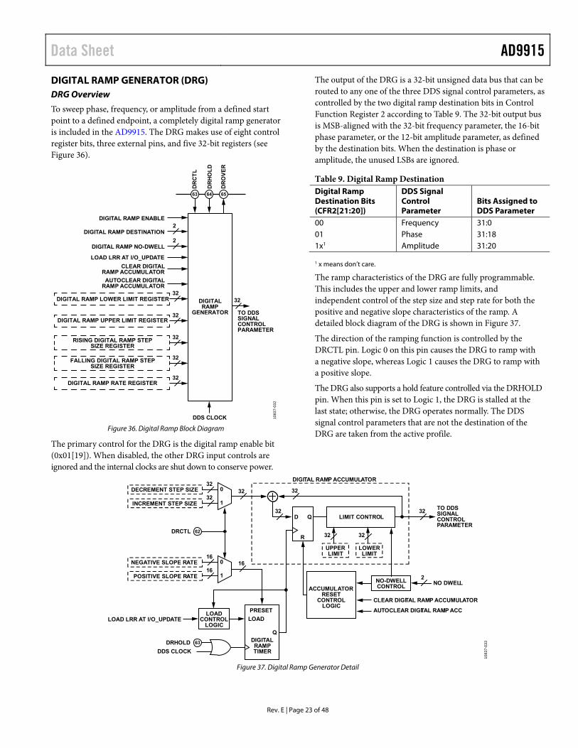
DIGITAL RAMP GENERATOR (DRG) DRG Overview
To sweep phase, frequency, or amplitude from a defined start point to a defined endpoint, a completely digital ramp generator is included in the AD9915. The DRG makes use of eight control register bits, three external pins, and five 32-bit registers (see Figure 36).
Figure 36. Digital Ramp Block Diagram
The primary control for the DRG is the digital ramp enable bit (0x01[19]). When disabled, the other DRG input controls are ignored and the internal clocks are shut down to conserve power.
The output of the DRG is a 32-bit unsigned data bus that can be routed to any one of the three DDS signal control parameters, as controlled by the two digital ramp destination bits in Control Function Register 2 according to Table 9. The 32-bit output bus is MSB-aligned with the 32-bit frequency parameter, the 16-bit phase parameter, or the 12-bit amplitude parameter, as defined by the destination bits. When the destination is phase or amplitude, the unused LSBs are ignored.
Table 9. Digital Ramp Destination Digital Ramp Destination Bits (CFR2[21:20])
DDS Signal Control Parameter
Bits Assigned to DDS Parameter
00 Frequency 31:0 01 Phase 31:18 1x1 Amplitude 31:20 1 x means don’t care.
The ramp characteristics of the DRG are fully programmable. This includes the upper and lower ramp limits, and independent control of the step size and step rate for both the positive and negative slope characteristics of the ramp. A detailed block diagram of the DRG is shown in Figure 37.
The direction of the ramping function is controlled by the DRCTL pin. Logic 0 on this pin causes the DRG to ramp with a negative slope, whereas Logic 1 causes the DRG to ramp with a positive slope.
The DRG also supports a hold feature controlled via the DRHOLD pin. When this pin is set to Logic 1, the DRG is stalled at the last state; otherwise, the DRG operates normally. The DDS signal control parameters that are not the destination of the DRG are taken from the active profile.
Figure 37. Digital Ramp Generator Detail
DR
CT
L
DDS CLOCK
DR
HO
LD
DR
OV
ER
DIGITAL RAMP ENABLE
LOAD LRR AT I/O_UPDATE
CLEAR DIGITALRAMP ACCUMULATOR
AUTOCLEAR DIGITALRAMP ACCUMULATOR
32
32
DIGITAL RAMP DESTINATION2
DIGITAL RAMP NO-DWELL2
32
32
63 64 65
32
32
TO DDSSIGNALCONTROLPARAMETER
DIGITALRAMP
GENERATOR
DIGITAL RAMP LOWER LIMIT REGISTER
RISING DIGITAL RAMP STEPSIZE REGISTER
DIGITAL RAMP UPPER LIMIT REGISTER
FALLING DIGITAL RAMP STEPSIZE REGISTER
DIGITAL RAMP RATE REGISTER
1083
7-03
2
DDS CLOCK
D Q
R
LOWERLIMIT
0
1
DECREMENT STEP SIZE
PRESET
Q
DRCTL
LOAD
CLEAR DIGITAL RAMP ACCUMULATOR
AUTOCLEAR DIGITAL RAMP ACC.
NO DWELL
LIMIT CONTROL
DIGITAL RAMP ACCUMULATOR
INCREMENT STEP SIZE
32
32
0
1
NEGATIVE SLOPE RATE
POSITIVE SLOPE RATE
16
16
32
16
62
DRHOLD 63
32
32
LOADCONTROL
LOGICLOAD LRR AT I/O_UPDATE
DIGITALRAMPTIMER
ACCUMULATORRESET
CONTROLLOGIC
NO-DWELLCONTROL
2
3232
TO DDSSIGNALCONTROLPARAMETER
UPPERLIMIT
32
1083
7-03
3

AD9915 Data Sheet
Rev. E | Page 24 of 48
DRG Slope Control
The core of the DRG is a 32-bit accumulator clocked by a programmable timer. The time base for the timer is the DDS clock, which operates at 1/24 fSYSCLK. The timer establishes the interval between successive updates of the accumulator. The positive (+Δt) and negative (−Δt) slope step intervals are independently programmable as given by
SYSCLKfP
t24
=∆+
SYSCLKfN
t24
=∆−
where P and N are the two 16-bit values stored in the 32-bit digital ramp rate register and control the step interval. N defines the step interval of the negative slope portion of the ramp. P defines the step interval of the positive slope portion of the ramp.
The step size of the positive (STEPP) and negative (STEPN) slope portions of the ramp are 32-bit values programmed into the 32-bit rising and falling digital ramp step size registers (0x06 and 0x07). Program each of the step sizes as an unsigned integer (the hardware automatically interprets STEPN as a negative value). The relationship between the 32-bit step size values and actual units of frequency, phase, or amplitude depend on the digital ramp destination bits. Calculate the actual frequency, phase, or amplitude step size by substituting STEPN or STEPP for M in the following equations as required:
SYSCLKfMStepFrequency
= 322
312MStepPhase π
= (radians)
29245MStepPhase =
(degrees)
FSIMStepAmplitude
= 322
Note that the frequency units are the same as those that represent fSYSCLK (MHz, for example). The amplitude units are the same as those that represent IFS, the full-scale output current of the DAC (mA, for example).
The phase and amplitude step size equations yield the average step size. Although the step size accumulates with 32-bit precision, the phase or amplitude destination exhibits only 16 bits or 12 bits, respectively. Therefore, at the destination, the actual phase or amplitude step is the accumulated 32-bit value truncated to 16 bits or 12 bits, respectively.
As described previously, the step interval is controlled by a 16-bit programmable timer. There are three events that can cause this timer to be reloaded prior to the expiration. One event occurs when the digital ramp enable bit transitions from cleared to set, followed by an input/output update. A second event is a change of state in the DRCTL pin. The third event is enabled using the load LRR at input/output update bit (0x00[15]).
DRG Limit Control
The ramp accumulator is followed by limit control logic that enforces an upper and lower boundary on the output of the ramp generator. Under no circumstances does the output of the DRG exceed the programmed limit values while the DRG is enabled. The limits are set through the 64-bit digital ramp limit register. Note that the upper limit value must be greater than the lower limit value to ensure normal operation.
DRG Accumulator Clear
The ramp accumulator can be cleared (that is, reset to 0) under program control. When the ramp accumulator is cleared, it forces the DRG output to the lower limit programmed into the digital ramp limit register.
With the limit control block embedded in the feedback path of the accumulator, resetting the accumulator is equivalent to presetting it to the lower limit value.

Data Sheet AD9915
Rev. E | Page 25 of 48
Figure 38. Normal Ramp Generation
Normal Ramp Generation
Normal ramp generation implies that both no-dwell bits are cleared (see the No-Dwell Ramp Generation section for details). In Figure 38, a sample ramp waveform is depicted with the required control signals. The top trace is the DRG output. The next trace down is the status of the DROVER output pin (assuming that the DRG over output enable bit is set). The remaining traces are control bits and control pins. The pertinent ramp parameters are also identified (upper and lower limits plus step size and Δt for the positive and negative slopes). Along the bottom, circled numbers identify specific events. These events are referred to by number (Event 1 and so on) in the following paragraphs.
In this example, the positive and negative slopes of the ramp are different to demonstrate the flexibility of the DRG. The parameters of both slopes can be programmed to make the positive and negative slopes the same.
Event 1—The digital ramp enable bit is set, which has no effect on the DRG output because the bit is not effective until an input/output update occurs.
Event 2—An input/output update registers the digital ramp enable bit. If DRCTL = 1 is in effect (the gray portion of the DRCTL trace), the DRG output immediately begins a positive slope (the gray portion of the DRG output trace). Otherwise, if DRCTL = 0, the DRG output is initialized to the lower limit.
Event 3—DRCTL transitions to Logic 1 to initiate a positive slope at the DRG output. In this example, the DRCTL pin is held long enough to cause the DRG to reach the programmed upper limit. The DRG remains at the upper limit until the ramp accumulator is cleared (DRCTL = 0) or the upper limit is reprogrammed to a higher value. In the latter case, the DRG immediately resumes the previous positive slope profile.
Event 4—DRCTL transitions to Logic 0 to initiate a negative slope at the DRG output. In this example, the DRCTL pin is held long enough to cause the DRG to reach the programmed lower limit. The DRG remains at the lower limit until DRCTL = 1, or until the lower limit is reprogrammed to a lower value. In the latter case, the DRG immediately resumes the previous negative slope profile.
Event 5—DRCTL transitions to Logic 1 for the second time, initiating a second positive slope.
Event 6—The positive slope profile is interrupted by DRHOLD transitioning to Logic 1. This stalls the ramp accumulator and freezes the DRG output at the last value.
Event 7—DRHOLD transitions to Logic 0, releasing the ramp accumulator and reinstating the previous positive slope profile.
Event 8—The clear digital ramp accumulator bit is set, which has no effect on the DRG because the bit is not effective until an input/output update is issued.
Event 9—An input/output update registers that the clear digital ramp accumulator bit is set, resetting the ramp accumulator and forcing the DRG output to the programmed lower limit. The DRG output remains at the lower limit until the clear condition is removed.
Event 10—The clear digital ramp accumulator bit is cleared, which has no effect on the DRG output because the bit is not effective until an input/output update is issued.
Event 11—An input/output update registers that the clear digital ramp accumulator bit is cleared, releasing the ramp accumulator; and the previous positive slope profile restarts.
DRG OUTPUT
LOWER LIMIT
UPPER LIMIT
DRCTL
DRHOLD
AUTOCLEAR DIGITALRAMP ACCUMULATOR
CLEAR DIGITALRAMP ACCUMULATOR
I/O_UPDATE
POSITIVESTEP SIZE
NEGATIVESTEP SIZE
P DDS CLOCK CYCLES N DDS CLOCK CYCLES 1 DDS CLOCK CYCLE
DIGITAL RAMP ENABLE
DROVER
CLE
AR
REL
EASE
AU
TOC
LEA
R
–Δt+Δt
1 2 3 4 5 6 7 8 9
10
11
12
13
1083
7-03
4

AD9915 Data Sheet
Rev. E | Page 26 of 48
Event 12—The autoclear digital ramp accumulator bit is set, which has no effect on the DRG output because the bit is not effective until an input/output update is issued.
Event 13—An input/output update registers that the autoclear digital ramp accumulator bit is set, resetting the ramp accumulator. However, with an automatic clear, the ramp accumulator is held in reset for only a single DDS clock cycle. This forces the DRG output to the lower limit, but the ramp accumulator is immediately made available for normal operation. In this example, the DRCTL pin remains Logic 1; therefore, the DRG output restarts the previous positive ramp profile.
No-Dwell Ramp Generation
The two no-dwell high and no-dwell low bits (0x01[18:17]) in CFR2 add to the flexibility of the DRG capabilities. During normal ramp generation, when the DRG output reaches the programmed upper or lower limit, it simply remains at the limit until the operating parameters dictate otherwise. However, during no-dwell operation, the DRG output does not necessarily remain at the limit. For example, if the digital ramp no-dwell high bit is set when the DRG reaches the upper limit, it automatically (and immediately) snaps to the lower limit (that is, it does not ramp back to the lower limit; it jumps to the lower limit). Likewise, when the digital ramp no-dwell low bit is set, and the DRG reaches the lower limit, it automatically (and immediately) snaps to the upper limit.
During no-dwell operation, the DRCTL pin is monitored for state transitions only; that is, the static logic level is immaterial.
During no-dwell high operation, a positive transition of the DRCTL pin initiates a positive slope ramp, which continues uninterrupted (regardless of any further activity on the DRCTL pin) until the upper limit is reached.
During no-dwell low operation, a negative transition of the DRCTL pin initiates a negative slope ramp, which continues uninterrupted (regardless of any further activity on the DRCTL pin) until the lower limit is reached.
Setting both no-dwell bits invokes a continuous ramping mode of operation; that is, the DRG output automatically oscillates between the two limits using the programmed slope parameters. Furthermore, the function of the DRCTL pin is slightly different. Instead of controlling the initiation of the ramp sequence, it only serves to change the direction of the ramp; that is, if the DRG output is in the midst of a positive slope and the DRCTL
pin transitions from Logic 1 to Logic 0, the DRG immediately switches to the negative slope parameters and resumes oscilla-tion between the limits. Likewise, if the DRG output is in the midst of a negative slope and the DRCTL pin transitions from Logic 0 to Logic 1, the DRG immediately switches to the positive slope parameters and resumes oscillation between the limits.
When both no-dwell bits are set, the DROVER signal produces a positive pulse (two cycles of the DDS clock) each time the DRG output reaches either of the programmed limits (assuming that the DRG over output enable bit (0x01[13]) is set).
A no-dwell high DRG output waveform is shown in Figure 39. The waveform diagram assumes that the digital ramp no-dwell high bit is set and has been registered by an input/output update. The status of the DROVER pin is also shown with the assumption that the DRG over output enable bit has been set.
The circled numbers in Figure 39 indicate specific events, which are explained as follows:
Event 1—Indicates the instant that an input/output update registers that the digital ramp enable bit is set.
Event 2—DRCTL transitions to Logic 1, initiating a positive slope at the DRG output.
Event 3—DRCTL transitions to Logic 0, which has no effect on the DRG output.
Event 4—Because the digital ramp no-dwell high bit is set, the moment that the DRG output reaches the upper limit, it imme-diately switches to the lower limit, where it remains until the next Logic 0 to Logic 1 transition of DRCTL.
Event 5—DRCTL transitions from Logic 0 to Logic 1, which restarts a positive slope ramp.
Event 6 and Event 7—DRCTL transitions are ignored until the DRG output reaches the programmed upper limit.
Event 8—Because the digital ramp no-dwell high bit is set, the moment that the DRG output reaches the upper limit, it immedi-ately switches to the lower limit, where it remains until the next Logic 0 to Logic 1 transition of DRCTL.
Operation with the digital ramp no-dwell low bit set (instead of the digital ramp no-dwell high bit) is similar, except that the DRG output ramps in the negative direction on a Logic 1 to Logic 0 transition of DRCTL and jumps to the upper limit upon reaching the lower limit.

Data Sheet AD9915
Rev. E | Page 27 of 48
Figure 39. No-Dwell High Ramp Generation
DROVER Pin
The DROVER pin provides an external signal to indicate the status of the DRG. Specifically, when the DRG output is at either of the programmed limits, the DROVER pin is Logic 1; otherwise, it is Logic 0. In the special case of both no-dwell bits set, the DROVER pin pulses positive for two DDS clock cycles each time the DRG output reaches either of the programmed limits.
Frequency Jumping Capability in DRG Mode
Another feature of the AD9915 allows the user to skip a predefined range of frequencies during a normal sweep. The frequency jump enable bit in CFR2 (0x01[14]) enables this functionality. When this bit is set, the sweeping logic monitors the instantaneous frequency. When it reaches the frequency point defined in the lower frequency jump register (0x09) on the next accumulation cycle, instead of accumulating a delta tuning word as in normal sweeping, it skips directly to the frequency value set in the upper frequency jump register (0x0A), and vice versa. Figure 40 shows how this feature works.
A second frequency jump can also be allowed if the frequency jump registers are reprogrammed before the sweeping is complete.
The following rules apply when this feature is enabled.
The frequency jump values must lie between the lower limit and upper limit of the frequency sweep range.
The lower frequency jump register value must be lower than that of the upper frequency jump register value.
Figure 40. Frequency vs. Time
POWER-DOWN CONTROL The AD9915 offers the ability to independently power down three specific sections of the device. Power-down functionality applies to the following:
Digital core DAC Input REF CLK clock circuitry
A power-down of the digital core disables the ability to update the serial/parallel input/output port. However, the digital power-down bit (0x00[7]) can still be cleared to prevent the possibility of a nonrecoverable state.
Software power-down is controlled via three independent power-down bits in CFR1. Software control requires that the EXT_PWR_DWN pin be forced to a Logic 0 state. In this case, setting the desired power-down bits (0x00[7:5]) via the serial input/output port powers down the associated functional block, whereas clearing the bits restores the function.
Alternatively, all three functions can be simultaneously powered down via external hardware control through the EXT_PWR_DWN pin. When this pin is forced to Logic 1, all four circuit blocks are powered down regardless of the state of the power-down bits; that is, the independent power-down bits in CFR1 are ignored and overridden when EXT_PWR_DWN is Logic 1.
Based on the state of the external power-down control bit, the EXT_PWR_DWN pin produces either a full power-down or a fast recovery power-down. The fast recovery power-down mode maintains power to the DAC bias circuitry and the PLL, VCO, and input clock circuitry. Although the fast recovery power-down does not conserve as much power as the full power-down, it allows the device to awaken very quickly from the power-down state.
UPPER LIMIT
P DDS CLOCK CYCLES
1 2 3 4 5 6 7 8
DRG OUTPUT
LOWER LIMIT
DRCTL
POSITIVESTEP SIZE
DROVER
+∆t
1083
7-03
5
FREQUENCY
t
UPPER LIMIT
0x09
0x0A
LOWER LIMIT
1083
7-03
6

AD9915 Data Sheet
Rev. E | Page 28 of 48
PROGRAMMING AND FUNCTION PINS The AD9915 is equipped with a 32-bit parallel port. The 32-bit port is for programming the internal registers of the device in either serial mode or parallel mode as well as allowing for direct modulation control of frequency (FTW), phase (POW), and amplitude (AMP).The state of the external function pins (F0
to F3) determines how the 32-bit parallel port is configured. Pin 28 to Pin 31 are the function pins. Refer to Table 10 for possible configurations.
Note that the OSK enable bit, CFR1[8], must be set to enable amplitude control, as shown in Table 10.
Table 10. Parallel Port Configurations
Function Pins, F[3:0]1 Mode Description
32-Bit Parallel Port Pin Assignment Bits[31:24]2 Bits[23:16]3 Bits[15:8]4 Bits[7:0]5
0000 Parallel programming mode Data[15:8] (optional)
Data[7:0] Address[7:0] Controls writes, reads, and 8-bit or 16-bit data-word. See the Parallel Programming section for details.
0001 Serial programming mode Not used Not used Not used Controls SCLK, SDIO, SDO, CS, and SYNCIO. See the Serial Programming section for details.
0010 Full 32 bits of direct frequency tuning word control. MSB and LSB aligned to parallel port pins
FTW[31:24] FTW[23:16] FTW[15:8] FTW[7:0]
0011 Full 32 bits of direct frequency tuning word control with different parallel port pin assignments
FTW[15:8] FTW[7:0] FTW[31:24] FTW[23:16]
0100 Full 16 bits of direct phase offset control and full 12 bits of direct amplitude control
POW[15:8] POW[7:0] AMP[11:8] AMP[7:0]
0101 Full 12 bits of direct amplitude control and full 16 bits of direct phase offset control
AMP[11:8] AMP[7:0] POW[15:8] POW[7:0]
0110 24 bits of partial FTW control and 8 bits of partial amplitude control
FTW[31:24] FTW[23:16] FTW[15:8] AMP[15:8]
0111 24 bits of partial FTW control and 8 bits of partial phase offset control
FTW[31:24] FTW[23:16] FTW[15:8] POW[15:8]
1000 24 bits of partial FTW control and 8 bits of partial amplitude control
FTW[31:24] FTW[23:16] FTW[15:8] AMP[7:0]
1001 24 bits of partial FTW control and 8 bits of partial phase offset control
FTW[31:24] FTW[23:16] FTW[15:8] POW[7:0]
1010 24 bits of partial FTW control and 8 bits of partial amplitude control
FTW[23:16] FTW[15:8] FTW[7:0] AMP[15:8]
1011 24 bits of partial FTW control and 8 bits of partial phase offset control
FTW[23:16] FTW[15:8] FTW[7:0] POW[15:8]
1100 24 bits of partial FTW control and 8 bits of partial amplitude control
FTW[23:16] FTW[15:8] FTW[7:0] AMP[7:0]
1101 24 bits of partial FTW control and 8 bits of partial phase offset control
FTW[23:16] FTW[15:8] FTW[7:0] POW[7:0]
1110 Not used Not used Not used Not used 1111 Not used Not used Not used Not used 1 Pin 31 to Pin 28. 2 Pin 68 to Pin 72, Pin 75 to 77. 3 Pin 78 to Pin 81, Pin 87, Pin 88, Pin 1, Pin 2. 4 Pin 3 to Pin 5, Pin 8 to Pin 12. 5 Pin 13 to Pin 15, Pin 18 to Pin 22.
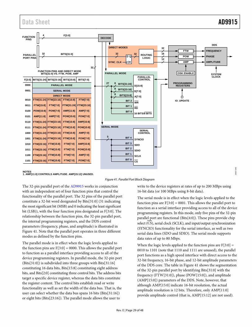
Data Sheet AD9915
Rev. E | Page 29 of 48
Figure 41. Parallel Port Block Diagram
The 32-pin parallel port of the AD9915 works in conjunction with an independent set of four function pins that control the functionality of the parallel port. The 32 pins of the parallel port constitute a 32-bit word designated by Bits[31:0] (31 indicating the most significant bit (MSB) and 0 indicating the least significant bit (LSB)), with the four function pins designated as F[3:0]. The relationship between the function pins, the 32-pin parallel port, the internal programming registers, and the DDS control parameters (frequency, phase, and amplitude) is illustrated in Figure 41. Note that the parallel port operates in three different modes as defined by the function pins.
The parallel mode is in effect when the logic levels applied to the function pins are F[3:0] = 0000. This allows the parallel port to function as a parallel interface providing access to all of the device programming registers. In parallel mode, the 32-pin port (Bits[31:0]) is subdivided into three groups with Bits[31:16] constituting 16 data bits, Bits[15:8] constituting eight address bits, and Bits[2:0] constituting three control bits. The address bits target a specific device register, whereas the data bits constitute the register content. The control bits establish read or write functionality as well as set the width of the data bus. That is, the user can select whether the data bus spans 16 bits (Bits[31:16]) or eight bits (Bits[23:16]). The parallel mode allows the user to
write to the device registers at rates of up to 200 MBps using 16-bit data (or 100 MBps using 8-bit data).
The serial mode is in effect when the logic levels applied to the function pins are F[3:0] = 0001. This allows the parallel port to function as a serial interface providing access to all of the device programming registers. In this mode, only five pins of the 32-pin parallel port are functional (Bits[4:0]). These pins provide chip select (CS), serial clock (SCLK), and input/output synchronization (SYNCIO) functionality for the serial interface, as well as two serial data lines (SDO and SDIO). The serial mode supports data rates of up to 80 Mbps.
When the logic levels applied to the function pins are F[3:0] = 0010 to 1101 (note that 1110 and 1111 are unused), the parallel port functions as a high speed interface with direct access to the 32-bit frequency, 16-bit phase, and 12-bit amplitude parameters of the DDS core. The table in Figure 41 shows the segmentation of the 32-pin parallel port by identifying Bits[31:0] with the frequency (FTW[31:0]), phase (POW[15:0]), and amplitude (AMP[15:0]) parameters of the DDS. Note, however, that although AMP[15:0] indicate 16-bit resolution, the actual amplitude resolution is 12 bits. Therefore, only AMP[11:0] provide amplitude control (that is, AMP[15:12] are not used).
PARALLELPORT PINS
4DECODE
D Q
CK
32 ROUTINGLOGIC
3232
32
27 8
8
8
WR
RD
DIRECT MODES
5
SDO
SYNCIO
SDIO
SCLK
CS
PARALLEL MODE
SERIAL MODE
FTW FREQUENCY
PHASE
AMPLITUDE
DDS32
16
12POW
AMP
0000
0011
0100
0101
0110
0111
1000
1001
1010
1011
1100
1101
0001
0010
PARALLEL MODE
SERIAL MODE
DIRECT MODE
OSK ENABLE
1083
7-04
6
NOTES1. AMP[11:0] CONTROLS AMPLITUDE. AMP[15:12] UNUSED.
FUNCTIONPINS
FUNCTION PINS AND DIRECT MODEBITS[31:0] VS. FTW, POW, AMP
F[3:0]
BITS[31:0]
F[3:0] BITS[31:24] BITS[23:16] BITS[15:8] BITS[7:0]
FTW[31:24]
FTW[15:8]
POW[15:8]
AMP[11:8]
FTW[31:24]
FTW[31:24]
FTW[31:24]
FTW[31:24]
FTW[23:16]
FTW[23:16]
FTW[23:16]
FTW[23:16]
FTW[23:16]
FTW[7:0]
POW[7:0]
AMP[7:0]
FTW[23:16]
FTW[23:16]
FTW[23:16]
FTW[23:16]
FTW[15:8]
FTW[15:8]
FTW[15:8]
FTW[15:8]
FTW[15:8]
FTW[31:24]
AMP[11:8]
POW[15:8]
FTW[15:8]
FTW[15:8]
FTW[15:8]
FTW[15:8]
FTW[7:0]
FTW[7:0]
FTW[7:0]
FTW[7:0]
FTW[7:0]
FTW[23:16]
AMP[7:0]
POW[7:0]
AMP[15:8]
POW[15:8]
AMP[7:0]
POW[7:0]
AMP[15:8]
POW[15:8]
AMP[7:0]
POW[7:0]
PROGRAMMINGREGISTERS
IO_UPDATE
BIT 4
BIT 3
BIT 2
BIT 1
BIT 0
SERIALCONTROL
SYSTEMCLOCK
SYNC_CLK
PARALLELCONTROL
BITS[31:24]
BITS[23:16]
BITS[15:8]
BIT 2
BIT 1
BIT 0
D[15:8]
D[7:0]
A[7:0]
16 BITS/8 BITS

AD9915 Data Sheet
Rev. E | Page 30 of 48
Furthermore, to make use of amplitude control, the user must be sure to program the OSK enable bit in the CFR1 register (0x00[8]) to Logic 1.
The combination of the F[3:0] pins and Bits[31:0] provides the AD9915 with unprecedented modulation capability by allowing the user direct control of the DDS parameters (frequency, phase, amplitude, or various combinations thereof). Furthermore, the parallel port operates at a sample rate equal to 1/16 of the system sample clock. This allows for updates of the DDS parameters at rates of up to 156 MSPS (assuming a 2.5 GHz system clock) allowing the AD9915 to accommodate applications with wideband modulation requirements.
Be aware that the frequency, phase, and amplitude changes applied at the parallel port travel to the DDS core over different paths, experiencing different propagation times (latency). Therefore, modulating more than one DDS parameter necessitates setting the device matched latency enable bit in the CFR2 register (0x01[15]), which equalizes the latency of each DDS parameter as it propagates from the parallel port to the DDS core. Note that high speed modulation requires a DAC reconstruction filter with sufficient bandwidth to accommodate the instantaneous time domain transitions.
Because direct access to the DDS parameters occurs via the FTW, POW, and AMP registers, the IO_UPDATE pin (see Figure 41) adds another layer of flexibility. To accommodate this functionality, the AD9915 provides a register control bit, parallel port streaming enable (0x00[17]). When this bit is set
to Logic 1, the parallel port operates without the need for an input/output update. When this bit is Logic 0, however, the device delivers the parallel port data to the appropriate registers (FTW, POW, AMP), but not to the DDS core. Data does not transfer to the DDS core until the user asserts the IO_UPDATE pin.
For example, suppose that an application requires frequency and amplitude modulation with full 32-bit frequency resolution and full 12-bit amplitude resolution. Note that none of the F[3:0] pin combinations supports such modulation capability directly. To circumvent this problem, set the parallel port streaming enable bit (0x00[17]) to Logic 0. This allows for the use of two direct mode cycles of the 32-pin parallel port, each with a different function pin setting, without affecting the DDS core until assertion of the IO_UPDATE pin. That is, during the first direct mode cycle, set the function pins to F[3:0] = 0010, which routes all 32 bits to the FTW register (frequency). On the next direct mode cycle, set the function pins to F[3:0] = 0100, which provides full 12-bit access to the AMP register (amplitude). Be aware, however, this also provides access to the POW register (phase); therefore, be sure keep the phase bits static. Next, toggle the IO_UPDATE pin, which synchronously transfers the new frequency and phase values from the FTW and POW registers to the DDS core. This mode of operation reduces the overall modulation rate by a factor of three because it requires two separate operations on the parallel port followed by an IO_UPDATE. However, this still allows for modulation sample rates as high as ~52 MSPS.

Data Sheet AD9915
Rev. E | Page 31 of 48
SERIAL PROGRAMMING To enable SPI operations, set Pin 28 (F0) to logic high and Pin 29 to Pin 31 (F1 to F3) to logic low. To program the AD9915 with a parallel interface, see the Parallel Programming section.
CONTROL INTERFACE—SERIAL INPUT/OUTPUT The AD9915 serial port is a flexible, synchronous serial commu-nications port allowing easy interface to many industry-standard microcontrollers and microprocessors. The serial input/output is compatible with most synchronous transfer formats.
The interface allows read/write access to all registers that configure the AD9915. MSB-first or LSB-first transfer formats are sup-ported. In addition, the serial interface port can be configured as a single pin input/output (SDIO) allowing a 2-wire interface, or it can be configured as two unidirectional pins for input/ output (SDIO and SDO), enabling a 3-wire interface. Two optional pins (I/O_SYNC and CS) enable greater flexibility for designing systems with the AD9915.
Table 11. Serial Input/Output Pin Description Pin No. Mnemonic Serial Input/Output Description 18 D4/SYNCIO SYNCIO 19 D3/SDO SDO 20 D2/SDIO/WR SDIO
21 D1/SCLK/RD SCLK
22 D0/CS/PWD CS—chip select
GENERAL SERIAL INPUT/OUTPUT OPERATION There are two phases to a serial communications cycle. The first is the instruction phase to write the instruction byte into the AD9915. The instruction byte contains the address of the register to be accessed and defines whether the upcoming data transfer is a write or read operation.
For a write cycle, Phase 2 represents the data transfer between the serial port controller to the serial port buffer. The number of bytes transferred is a function of the register being accessed. For example, when accessing Control Function Register 2 (Address 0x01), Phase 2 requires that four bytes be transferred. Each bit of data is registered on each corresponding rising edge of SCLK. The serial port controller expects that all bytes of the register be accessed; otherwise, the serial port controller is put out of sequence for the next communication cycle. However, one way to write fewer bytes than required is to use the SYNCIO pin feature. The SYNCIO pin function can abort an input/output operation and reset the pointer of the serial port controller. After a SYNCIO, the next byte is the instruction byte. Note that every completed byte written prior to a SYNCIO is preserved in the serial port buffer. Partial bytes written are not preserved. At the completion of any communication cycle, the AD9915 serial port controller expects the next eight rising SCLK edges to be the instruction byte for the next communication cycle.
After a write cycle, the programmed data resides in the serial port buffer and is inactive. I/O_UPDATE transfers data from the serial port buffer to active registers. The input/output update can be sent either after each communication cycle or when all serial operations are complete. In addition, a change in profile pins can initiate an input/output update.
For a read cycle, Phase 2 is the same as the write cycle with the following differences: data is read from the active registers, not the serial port buffer, and data is driven out on the falling edge of SCLK.
Note that, to read back any profile register (0x0B to 0x1A), the three external profile pins must be used. For example, if the profile register is Profile 5 (0x15), the PS[0:2] pins must equal 101.This is not required to write to the profile registers.
INSTRUCTION BYTE The instruction byte contains the following information as shown in the instruction byte information bit map.
Instruction Byte Information Bit Map MSB LSB
I7 I6 I5 I4 I3 I2 I1 I0
R/W X A5 A4 A3 A2 A1 A0
R/W—Bit 7 of the instruction byte determines whether a read or write data transfer occurs after the instruction byte write. Logic 1 indicates a read operation. Logic 0 indicates a write operation.
X—Bit 6 of the instruction byte is don’t care.
A5, A4, A3, A2, A1, A0—Bit 5, Bit 4, Bit 3, Bit 2, Bit 1, and Bit 0 of the instruction byte determine which register is accessed during the data transfer portion of the communications cycle.
SERIAL INPUT/OUTPUT PORT PIN DESCRIPTIONS SCLK—Serial Clock
The serial clock pin synchronizes data to and from the AD9915 and to run the internal state machines.
CS—Chip Select Bar
CS is an active low input that allows more than one device on the same serial communications line. The SDO and SDIO pins go to a high impedance state when this input is high. If driven high during any communications cycle, that cycle is suspended until CS is reactivated low. Chip select (CS) can be tied low in systems that maintain control of SCLK.
SDIO—Serial Data Input/Output
Data is always written into the AD9915 on this pin. However, this pin can be used as a bidirectional data line. Bit 1 of CFR1 (0x00) controls the configuration of this pin. The default is Logic 0, which configures the SDIO pin as bidirectional.

AD9915 Data Sheet
Rev. E | Page 32 of 48
SDO—Serial Data Out
Data is read from this pin for protocols that use separate lines for transmitting and receiving data. When the AD9915 operates in single bidirectional input/output mode, this pin does not output data and is set to a high impedance state.
SYNCIO—Input/Output Reset
SYNCIO synchronizes the input/output port state machines without affecting the contents of the addressable registers. An active high input on the SYNCIO pin causes the current communication cycle to abort. After SYNCIO returns low (Logic 0), another communication cycle can begin, starting with the instruction byte write.
I/O_UPDATE—Input/Output Update
The input/output update initiates the transfer of written data from the serial or parallel input/output port buffer to active registers. I/O_UPDATE is active on the rising edge, and the pulse width must be greater than one SYNC_CLK period.
SERIAL INPUT/OUTPUT TIMING DIAGRAMS Figure 42 through Figure 45 provide basic examples of the timing relationships between the various control signals of the serial input/output port. Most of the bits in the register map are not transferred to the internal destinations until assertion of an input/output update, which is not included in the timing diagrams that follow.
Note that the SCLK stall condition between the instruction byte cycle and data transfer cycle in Figure 42 to Figure 45 is not required.
MSB/LSB TRANSFERS The AD9915 serial port can support both most significant bit (MSB) first or least significant bit (LSB) first data formats. This functionality is controlled by Bit 0 in CFR1 (0x00). The default format is MSB first. If LSB first is active, all data, including the instruction byte, must follow LSB-first convention. Note that the highest number found in the bit range column for each register is the MSB, and the lowest number is the LSB for that register.
Figure 42. Serial Port Write Timing, Clock Stall Low
Figure 43. 3-Wire Serial Port Read Timing, Clock Stall Low
Figure 44. Serial Port Write Timing, Clock Stall High
Figure 45. 2-Wire Serial Port Read Timing, Clock Stall High
I7SDIO
INSTRUCTION CYCLE DATA TRANSFER CYCLE
SCLK
CS
I6 I5 I4 I3 I2 I1 I0 D7 D6 D5 D4 D3 D2 D1 D0
1083
7-03
7DO7
INSTRUCTION CYCLE DATA TRANSFER CYCLE
DON'T CAREI7 I6 I5 I4 I3 I2 I1 I0SDIO
SCLK
CS
SDO DO6 DO5 DO4 DO3 DO2 DO1 DO010
837-
038
I7SDIO
INSTRUCTION CYCLE DATA TRANSFER CYCLE
SCLK
CS
I6 I5 I4 I3 I2 I1 I0 D7 D6 D5 D4 D3 D2 D1 D0
1083
7-03
9
I7SDIO
INSTRUCTION CYCLE DATA TRANSFER CYCLE
SCLK
CS
I6 I5 I4 I3 I2 I1 I0 DO7 DO6 DO5 DO4 DO3 DO2 DO1 DO0
1083
7-04
0

Data Sheet AD9915
Rev. E | Page 33 of 48
PARALLEL PROGRAMMING (8-/16-BIT) The state of the external function pins (F0 to F3) determine the type of interface used by the AD9915. Pin 28 to Pin 31 are dedicated function pins. To enable the parallel mode interface set Pin 28 to Pin 31 to logic low.
Parallel programming consists of eight address lines and either eight or 16 bidirectional data lines for read/write operations. The logic state on Pin 22 determines the width of the data lines used. A logic low on Pin 22 sets the data width to eight bits, and logic high sets the data width to 16 bits. In addition, parallel mode has dedicated write/read control inputs. If 16-bit mode is used, the upper byte, Bits[15:8], goes to the addressed register and the lower byte, Bits[7:0], goes to the adjacent lower address.
Parallel input/output operation allows write access to each byte of any register in a single input/output operation. Readback capability for each register is included to ease designing with the AD9915.
Table 12. Parallel Port Read Timing (See Figure 46) Parameter Value Unit Test Conditions/Comments tADV 92 ns max Address to data valid time tAHD 0 ns min Address hold time to RD signal
inactive tRDLOV 69 ns max RD low to output valid
tRDHOZ 50 ns max RD high to data three-state
tRDLOW 69 ns max RD signal minimum low time
tRDHIGH 50 ns max RD signal minimum high time
Table 13. Parallel Port Write Timing (See Figure 47) Parameter Value Unit Test Conditions/Comments tASU 1 ns Address setup time to WR
signal active tDSU 3.8 ns Data setup time to WR signal
active tAHD 0 ns Address hold time to WR
signal inactive tDHD 0 ns Data hold time to WR signal
inactive tWRLOW 2.1 ns WR signal minimum low time
tWRHIGH 3.8 ns WR signal minimum high time
tWR 10.5 ns Minimum write time
Figure 46. Parallel Port Read Timing Diagram
Figure 47. Parallel Port Write Timing Diagram
A1
D1
A2
D2
A3
D3
A[7:0]
RD
D[7:0] ORD[15:0]
tRDHOZ
tRDHIGHtRDLOW
tRDLOV
tADVtAHD 1083
7-04
1
A1 A2 A3
D1 D2 D3
A[7:0]
WR
D[7:0] ORD[15:0]
tWR
tASU tAHD
tWRHIGH tDHD
tDSU
tWRLOW
1083
7-04
2
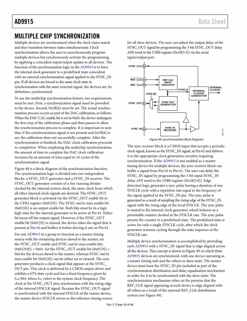
AD9915 Data Sheet
Rev. E | Page 34 of 48
MULTIPLE CHIP SYNCHRONIZATION Multiple devices are synchronized when the clock states match and they transition between states simultaneously. Clock synchronization allows the user to asynchronously program multiple devices but synchronously activate the programming by applying a coincident input/output update to all devices. The function of the synchronization logic in the AD9915 is to force the internal clock generator to a predefined state coincident with an external synchronization signal applied to the SYNC_IN pin. If all devices are forced to the same clock state in synchronization with the same external signal, the devices are, by definition, synchronized.
To use the multichip synchronization feature, two requirements must be met. First, a synchronization signal must be provided to the device. Second, 0x1B[6] must be set. The actual synchro-nization process occurs as part of the DAC calibration, as follows. When the DAC CAL enable bit is set in 0x03, the device undergoes the first step of the calibration phase and then pauses to allow the synchronization process to complete. It is important to note that, if the synchronization signal is not present and 0x1B[6] is set, the calibration does not successfully complete. After the synchronization is finished, the DAC clock calibration proceeds to completion. When employing the multichip synchronization, the amount of time to complete the DAC clock calibration increases by an amount of time equal to 16 cycles of the synchronization signal.
Figure 48 is a block diagram of the synchronization function. The synchronization logic is divided into two independent blocks: a SYNC_OUT generator and a SYNC_IN receiver. The SYNC_OUT generator consists of a free running divider clocked by the internal system clock, the same clock from which all other internal clock signals are derived. The SYNC_OUT generator block is activated via the SYNC_OUT enable bit in the CFR2 register (0x01[9]). The SYNC out/in mux enable bit (0x01[8]) is an output enable bit. Both bits must be in a logic high state for the internal generator to be active at Pin 61. Either bit turns off the output signal. However, if the SYNC_OUT enable bit (0x01[9]) is cleared, the device takes the signal that is present at Pin 62 and buffers it before driving it out on Pin 61.
For one AD9915 in a group to function as a master timing source with the remaining devices slaved to the master, set the SYNC_OUT enable and SYNC out/in mux enable bits (0x01[9:8]) = 0x03. Set the SYNC_OUT enable bit (0x01[9]) = 0x0 for the devices slaved to the master, whereas SYNC out/in mux enable bit (0x01[8]) can be either set or cleared. The sync generator produces a clock signal that appears at the SYNC_ OUT pin. This clock is delivered by a CMOS output driver and exhibits a 67% duty cycle and has a fixed frequency given by fSYS/384, where fSYS refers to the system clock frequency. The clock at the SYNC_OUT pins synchronizes with the rising edge of the internal SYSCLK signal. Because the SYNC_OUT signal is synchronized with the internal SYSCLK of the master device, the master device SYSCLK serves as the reference timing source
for all slave devices. The user can adjust the output delay of the SYNC_OUT signal by programming the 3-bit SYNC_OUT delay ADJ word in the USR0 register (0x1B[5:3]) via the serial input/output port.
Figure 48. Synchronization Block Diagram
The sync receiver block is a CMOS input that accepts a periodic clock signal, known as the SYNC_IN signal, at Pin 62 and delivers it to the appropriate clock generation circuitry requiring synchronization. If the AD9915 is not enabled as a master timing device for multiple devices, the sync receiver block can buffer a signal from Pin 62 to Pin 61. The user can delay the SYNC_IN signal by programming the 3-bit input SYNC_IN delay ADJ word in the USR0 register (0x1B[2:0]). Edge detection logic generates a sync pulse having a duration of one SYSCLK cycle with a repetition rate equal to the frequency of the signal applied to the SYNC_IN pin. The sync pulse is generated as a result of sampling the rising edge of the SYNC_IN signal with the rising edge of the local SYSCLK. The sync pulse is routed to the internal clock generator, which behaves as a presettable counter clocked at the SYSCLK rate. The sync pulse presets the counter to a predefined state. The predefined state is active for only a single SYSCLK cycle, after which the clock generator resumes cycling through the state sequence at the SYSCLK rate.
Multiple device synchronization is accomplished by providing each AD9915 with a SYNC_IN signal that is edge aligned across all the devices. This concept is shown in Figure 49, in which three AD9915 devices are synchronized, with one device operating as a master timing unit and the others as slave units. The master device must have the SYNC_IN pin included as part of the synchronization distribution and delay equalization mechanism in order for it to be synchronized with the slave units. The synchronization mechanism relies on the premise that the REF_CLK signal appearing at each device is edge aligned with all others as a result of the external REF_CLK distribution system (see Figure 49).
REF_CLK
REF_CLK
SYSCLK
1083
7-04
7
SYNC_CLK 82
54
55
61
62
REF CLKINPUT
CIRCUITRY
CFR2 [9]
SYNC_OUT
SYNC_IN
INTERNALCLOCKS
GENERATOR
SYNC OUTGENERATOR
INTERNALCLOCKS
SYNC INRECEIVER

Data Sheet AD9915
Rev. E | Page 35 of 48
The synchronization mechanism begins with the clock distribution and delay equalization block, which ensures all devices receive an edge aligned REF_CLK signal.
However, even though the REF_CLK signal is edge aligned among all devices, this alone does not guarantee that the clock state of each internal clock generator is coordinated with the others. This is the role of the synchronization redistribution circuit, which accepts the SYNC_OUT signal generated by the master device and redistributes it to the SYNC_IN input of the slave units (as well as feeding it back to the master). The goal of the redistributed SYNC_OUT signal from the master device is to deliver an edge aligned SYNC_IN signal to all of the sync receivers. Assuming that all devices share the same REF_CLK edge (due to the clock distribution and delay equalization block) and all devices share the same SYNC_IN edge (due to the synchronization distribution and delay equalization block), all devices generate an internal sync pulse in unison and the synchronized sync pulses cause all of the devices to assume the same predefined clock state simultaneously; that is, the internal clocks of all devices become fully synchronized. The synchronization mechanism depends on the reliable generation of a sync pulse by the edge detection block in the sync receiver. Generation of a valid sync pulse, however, requires proper sampling of the rising edge of the SYNC_IN signal with the rising edge of the local SYSCLK. If the edge timing of these signals fails to meet the setup or hold time requirements of the internal latches in the edge detection circuitry, the proper generation of the sync pulse is in jeopardy.
Ambient operating temperature and self heating of the AD9915 must also be considered when attempting to synchronize multiple
devices. In general, the propagation delay from the SYNC_IN pin to the internal clock generators is fixed for a given operating temperature. However, large temperature differences between devices or rapid increases in device temperature at power-up increase the complexity of synchronization.
Table 14 and Table 15 display the delay time increment for both SYNC_IN and SYNC_OUT vs. the corresponding register values, from 0 to 7.
Table 14. SYNC_IN Delay (Total Delay = 1.2 ns) Delay Step Increment, Typ (ns) 0 to 1 0.26 1 to 2 0.15 2 to 3 0.15 3 to 4 0.15 4 to 5 0.15 5 to 6 0.17 6 to 7 0.17
Table 15. SYNC_OUT Delay (Total Delay = 1.97 ns) Delay Step Increment, Typ (ns) 0 to 1 0.17 1 to 2 0.3 2 to 3 0.3 3 to 4 0.3 4 to 5 0.3 5 to 6 0.3 6 to 7 0.3
Figure 49. Configuration of Multiple Devices to Be Synchronized
SYNCIN
SYNCOUT
REF_CLKAD9915NUMBER 1 MASTER DEVICEFPGA
DATA
FPGA
DATA
FPGA
DATA
EDGEALIGNED
AT REF_CLKINPUTS
EDGEALIGNED
AT SYNC_ININPUTS
PDC
LK
SYNCIN
SYNCOUT
REF_CLKAD9915NUMBER 2
PDC
LK
SYNCIN
SYNCOUT
REF_CLKAD9915NUMBER 3
PDC
LK
(FOR EXAMPLE AD951x)
CLOCK DISTRIBUTIONAND
DELAY EQUALIZATION
SYNCHRONIZATIONDISTRIBUTION AND
DELAY EQUALIZATION(FOR EXAMPLE AD951x)
1083
7-05
3
CLOCKSOURCE

AD9915 Data Sheet
Rev. E | Page 36 of 48
REGISTER MAP AND BIT DESCRIPTIONS Table 16. Register Map Register Name (Serial Address)
Bit Range (Parallel Address)
Bit 7 (MSB) Bit 6 Bit 5 Bit 4 Bit 3 Bit 2 Bit 1
Bit 0 (LSB)
Default Value (Hex)1
CFR1—Control Function Register 1 (0x00)
[7:0] (0x00) Digital power-down
DAC power-down
REF CLK input power-down
Open External power-down control
Open SDIO input only
LSB first mode
0x08
[15:8] (0x01)
Load LRR at input/ output update
Autoclear digital ramp accumu-lator
Autoclear phase accumu-lator
Clear digital ramp accumulator
Clear phase accumulator
Open External OSK enable
OSK enable
0x00
[23:16] (0x02)
Open Parallel port streaming enable
Enable sine output
0x01
[31:24] (0x03)
Open VCO cal enable
0x00
CFR2—Control Function Register 2 (0x01)
[7:0] (0x04)
Open 0x00
[15:8] (0x05)
Matched latency enable
Frequency jump enable
DRG over output enable
Open SYNC_CLK enable
SYNC_CLK invert
SYNC_OUT enable
SYNC out/ in mux enable
0x09
[23:16] (0x06)
Profile mode enable
Parallel data port enable
Digital ramp destination Digital ramp enable
Digital ramp no-dwell high
Digital ramp no-dwell low
Program modulus enable
0x00
[31:24] (0x07)
Open 0x00
CFR3—Control Function Register 3 (0x02)
[7:0] (0x08)
Open Manual ICP selection
ICP[2:0] Lock detect enable
Minimum LDW[1:0] 0x1C
[15:8] (0x09)
Feedback Divider N[7:0] 0x19
[23:16] (0x0A)
Open Input divider reset
Input divider[1:0] Doubler enable
PLL enable PLL input divider enable
Doubler clock edge
0x00
[31:24] (0x0B)
Open 0x00
CFR4—Control Function Register 4 (0x03)
[7:0] (0x0C)
Requires register default value settings (0x20) 0x20
[15:8] (0x0D)
Requires register default value settings (0x21) 0x21
[23:16] (0x0E)
Requires register default value settings (0x05) 0x05
[31:24] (0x0F)
Open Auxiliary divider power-down
DAC CAL clock power-down
DAC CAL enable2
0x00
Digital Ramp Lower Limit Register (0x04)
[7:0] (0x10)
Digital ramp lower limit[7:0] 0x00
[15:8] (0x11)
Digital ramp lower limit[15:8] 0x00
[23:16] (0x12)
Digital ramp lower limit[23:16] 0x00
[31:24] (0x13)
Digital ramp lower limit[31:24] 0x00

Data Sheet AD9915
Rev. E | Page 37 of 48
Register Name (Serial Address)
Bit Range (Parallel Address)
Bit 7 (MSB) Bit 6 Bit 5 Bit 4 Bit 3 Bit 2 Bit 1
Bit 0 (LSB)
Default Value (Hex)1
Digital Ramp Upper Limit Register (0x05)
[7:0] (0x14) Digital ramp upper limit[7:0] 0x00
[15:8] (0x15)
Digital ramp upper limit[15:8] 0x00
[23:16] (0x16)
Digital ramp upper limit[23:16] 0x00
[31:24] (0x17)
Digital ramp upper limit[31:24] 0x00
Rising Digital Ramp Step Size Register (0x06)
[7:0] (0x18)
Rising digital ramp increment step size[7:0] N/A
[15:8] (0x19)
Rising digital ramp increment step size[15:8] N/A
[23:16] (0x1A)
Rising digital ramp increment step size[23:16] N/A
[31:24] (0x1B)
Rising digital ramp increment step size[31:24] N/A
Falling Digital Ramp Step Size Register (0x07)
[7:0] (0x1C)
Falling digital ramp decrement step size[7:0] N/A
[15:8] (0x1D)
Falling digital ramp decrement step size[15:8] N/A
[23:16] (0x1E)
Falling digital ramp decrement step size[23:16] N/A
[31:24] (0x1F)
Falling digital ramp decrement step size[31:24] N/A
Digital Ramp Rate Register (0x08)
[7:0] (0x20)
Digital ramp positive slope rate[7:0] N/A
[15:8] (0x21)
Digital ramp positive slope rate[15:8] N/A
[23:16] (0x22)
Digital ramp negative slope rate[7:0] N/A
[31:24] (0x23)
Digital ramp negative slope rate[15:8] N/A
Lower Frequency Jump Register (0x09)
[7:0] (0x24)
Lower frequency jump point[7:0] 0x00
[15:8] (0x25)
Lower frequency jump point[15:8] 0x00
[23:16] (0x26)
Lower frequency jump point[23:16] 0x00
[31:24] (0x27)
Lower frequency jump point[31:24] 0x00
Upper Frequency Jump Register (0x0A)
[7:0] (0x28)
Upper frequency jump point[7:0] 0x00
[15:8] (0x29)
Upper frequency jump point[15:8] 0x00
[23:16] (0x2A)
Upper frequency jump point[23:16] 0x00
[31:24] (0x2B)
Upper frequency jump point[31:24] 0x00
Profile 0 (P0) Frequency Tuning Word 0 Register (0x0B)
[7:0] (0x2C)
Frequency Tuning Word 0[7:0] 0x00
[15:8] (0x2D)
Frequency Tuning Word 0[15:8] 0x00
[23:16] (0x2E)
Frequency Tuning Word 0[23:16] 0x00
[31:24] (0x2F)
Frequency Tuning Word 0[31:24] 0x00

AD9915 Data Sheet
Rev. E | Page 38 of 48
Register Name (Serial Address)
Bit Range (Parallel Address)
Bit 7 (MSB) Bit 6 Bit 5 Bit 4 Bit 3 Bit 2 Bit 1
Bit 0 (LSB)
Default Value (Hex)1
Profile 0 (P0) Phase/ Amplitude Register (0x0C)
[7:0] (0x30)
Phase Offset Word 0[7:0] 0x00
[15:8] (0x31)
Phase Offset Word 0[15:8] 0x00
[23:16] (0x32)
Amplitude Scale Factor 0[7:0] 0x00
[31:24] (0x33)
Open Amplitude Scale Factor 0[11:8] 0x00
Profile 1 (P1) Frequency Tuning Word 1 Register (0x0D)
[7:0] (0x34)
Frequency Tuning Word 1[7:0] N/A
[15:8] (0x35)
Frequency Tuning Word 1[15:8] N/A
[23:16] (0x36)
Frequency Tuning Word 1[23:16] N/A
[31:24] (0x37)
Frequency Tuning Word 1[31:24] N/A
Profile 1 (P1) Phase/ Amplitude Register (0x0E)
[7:0] (0x38)
Phase Offset Word 1[7:0] N/A
[15:8] (0x39)
Phase Offset Word 1[15:8] N/A
[23:16] (0x3A)
Amplitude Scale Factor 1[7:0] N/A
[31:24] (0x3B)
Open Amplitude Scale Factor 1[11:8] N/A
Profile 2 (P2) Frequency Tuning Word 2 Register (0x0F)
[7:0] (0x3C)
Frequency Tuning Word 2[7:0] N/A
[15:8] (0x3D)
Frequency Tuning Word 2[15:8] N/A
[23:16] (0x3E)
Frequency Tuning Word 2[23:16] N/A
[31:24] (0x3F)
Frequency Tuning Word 2[31:24] N/A
Profile 2 (P2) Phase/ Amplitude Register (0x10)
[7:0] (0x40)
Phase Offset Word 2[7:0] N/A
[15:8] (0x41)
Phase Offset Word 2[15:8] N/A
[23:16] (0x42)
Amplitude Scale Factor 2[7:0] N/A
[31:24] (0x43)
Open Amplitude Scale Factor 2[11:8] N/A
Profile 3 (P3) Frequency Tuning Word 3 Register (0x11)
[7:0] (0x44)
Frequency Tuning Word 3[7:0] N/A
[15:8] (0x45)
Frequency Tuning Word 3[15:8] N/A
[23:16] (0x46)
Frequency Tuning Word 3[23:16] N/A
[31:24] (0x47)
Frequency Tuning Word 3[31:24] N/A
Profile 3 (P3) Phase/ Amplitude Register (0x12)
[7:0] (0x48)
Phase Offset Word 3[7:0] N/A
[15:8] (0x49)
Phase Offset Word 3[15:8] N/A
[23:16] (0x4A)
Amplitude Scale Factor 3[7:0] N/A
[31:24] (0x4B)
Open Amplitude Scale Factor 3[11:8] N/A

Data Sheet AD9915
Rev. E | Page 39 of 48
Register Name (Serial Address)
Bit Range (Parallel Address)
Bit 7 (MSB) Bit 6 Bit 5 Bit 4 Bit 3 Bit 2 Bit 1
Bit 0 (LSB)
Default Value (Hex)1
Profile 4 (P4) Frequency Tuning Word 4 Register (0x13)
[7:0] (0x4C)
Frequency Tuning Word 4[7:0] N/A
[15:8] (0x4D)
Frequency Tuning Word 4[15:8] N/A
[23:16] (0x4E)
Frequency Tuning Word 4[23:16] N/A
[31:24] (0x4F)
Frequency Tuning Word 4[31:24] N/A
Profile 4 (P4) Phase/ Amplitude Register (0x14)
[7:0] (0x50)
Phase Offset Word 4[7:0] N/A
[15:8] (0x51)
Phase Offset Word 4[15:8] N/A
[23:16] (0x52)
Amplitude Scale Factor 4[7:0] N/A
[31:24] (0x53)
Open Amplitude Scale Factor 4[11:8] N/A
Profile 5 (P5) Frequency Tuning Word 5 Register (0x15)
[7:0] (0x54)
Frequency Tuning Word 5[7:0] N/A
[15:8] (0x55)
Frequency Tuning Word 5[15:8] N/A
[23:16] (0x56)
Frequency Tuning Word 5[23:16] N/A
[31:24] (0x57)
Frequency Tuning Word 5[31:24] N/A
Profile 5 (P5) Phase/ Amplitude Register (0x16)
[7:0] (0x58)
Phase Offset Word 5[7:0] N/A
[15:8] (0x59)
Phase Offset Word 5[15:8] N/A
[23:16] (0x5A)
Amplitude Scale Factor 5[7:0] N/A
[31:24] (0x5B)
Open Amplitude Scale Factor 5[11:8] N/A
Profile 6 (P6) Frequency Tuning Word 6 Register (0x17)
[7:0] (0x5C)
Frequency Tuning Word 6[7:0] N/A
[15:8] (0x5D)
Frequency Tuning Word 6[15:8] N/A
[23:16] (0x5E)
Frequency Tuning Word 6[23:16] N/A
[31:24] (0x5F)
Frequency Tuning Word 6[31:24] N/A
Profile 6 (P6) Phase/ Amplitude Register (0x18)
[7:0] (0x60)
Phase Offset Word 6[7:0] N/A
[15:8] (0x61)
Phase Offset Word 6[15:8] N/A
[23:16] (0x62)
Amplitude Scale Factor 6[7:0] N/A
[31:24] (0x63)
Open Amplitude Scale Factor 6[11:8] N/A
Profile 7 (P7) Frequency Tuning Word 7 Register (0x19)
[7:0] (0x64)
Frequency Tuning Word 7[7:0] N/A
[15:8] (0x65)
Frequency Tuning Word 7[15:8] N/A
[23:16] (0x66)
Frequency Tuning Word 7[23:16] N/A
[31:24] (0x67)
Frequency Tuning Word 7[31:24] N/A

AD9915 Data Sheet
Rev. E | Page 40 of 48
Register Name (Serial Address)
Bit Range (Parallel Address)
Bit 7 (MSB) Bit 6 Bit 5 Bit 4 Bit 3 Bit 2 Bit 1
Bit 0 (LSB)
Default Value (Hex)1
Profile 7 (P7) Phase/ Amplitude Register (0x1A)
[7:0] (0x68)
Phase Offset Word 7[7:0] N/A
[15:8] (0x69)
Phase Offset Word 7[15:8] N/A
[23:16] (0x6A)
Amplitude Scale Factor 7[7:0] N/A
[31:24] (0x6B)
Open Amplitude Scale Factor 7[11:8] N/A
USR0 (0x1B) [7:0] (0x6C)
Reserved CAL with SYNC
SYNC_OUT delay ADJ[2:0] SYNC_IN delay ADJ[2:0] 0x00
[15:8] (0x6D)
Requires register default value settings (0x08) 0x08
[23:16] (0x6E)
Requires register default value settings (0x00) 0x00
[31:24] (0x6F)
Open PLL lock Read only
1 A master reset is required after power up. The master reset returns the internal registers to the default values. 2 The DAC CAL enable bit must be manually set and then cleared after each power-up and every time REF CLK or the internal system clock is changed. This initiates an
internal calibration routine to optimize the setup and hold times for internal DAC timing. Failure to calibrate degrades ac performance or makes the part nonfunctional.

Data Sheet AD9915
Rev. E | Page 41 of 48
REGISTER BIT DESCRIPTIONS The serial input/output port registers span an address range of 0 to 27 (0x00 to 0x1B in hexadecimal notation). This represents a total of 28 individual serial registers. If programming in parallel mode, the number of parallel registers increases to 112 individual parallel registers. Additionally, the registers are assigned names according to the functionality. In some cases, a register is given a mnemonic descriptor. For example, the register at Serial Address 0x00 is named Control Function Register 1 and is assigned the mnemonic CFR1.
This section provides a detailed description of each bit in the AD9915 register map. For cases in which a group of bits serves a specific function, the entire group is considered a binary word and is described in aggregate.
This section is organized in sequential order of the serial addresses of the registers. Each subheading includes the register name and optional register mnemonic (in parentheses). Also given is the serial address in hexadecimal format and the number of bytes assigned to the register.
Following each subheading is a table containing the individual bit descriptions for that particular register. The location of the bit(s) in the register is indicated by a single number or a pair of numbers separated by a colon; that is, a pair of numbers (A:B) indicates a range of bits from the most significant (A) to the least significant (B). For example, [5:2] implies Bit Position 5 to Bit Position 2, inclusive, with Bit 0 identifying the LSB of the register.
Unless otherwise stated, programmed bits are not transferred to the internal destinations until the assertion of the I/O_UPDATE pin or a profile pin change.
Control Function Register 1 (CFR1)—Address 0x00
Table 17. Bit Description for CFR1 Bits Mnemonic Description [31:25] Open 24 VCO cal enable 1 = initializes the auto internal PLL calibration. The calibration is required if the PLL is to
provide the internal system clock. Must first be reset to Logic 0 before another calibration can be issued.
[23:18] Open Open. 17 Parallel port streaming enable 0 = the 32 bit parallel port needs an input/output update to activate or register any FTW, POW,
or AMP data presented to the 32-bit parallel port.
1 = the parallel port continuously samples data on the 32 input pins using SYNC_CLK and multiplexes the value of FTW/POW/AMP accordingly, per the configuration of the F0 to F3 pins, without the need of an input/output update. Data must meet the setup and hold times of the SYNC_CLK rising edge. If the function pins are used dynamically to alter data between parameters, they must also meet the timing of the SYNC_CLK edge.
16 Enable sine output 0 = cosine output of the DDS is selected. 1 = sine output of the DDS is selected (default).
15 Load LRR at input/output update Ineffective unless CFR2[19] = 1. 0 = normal operation of the digital ramp timer (default). 1 = interrupts the digital ramp timer operation to load a new linear ramp rate (LRR) value any
time I/O_UPDATE is asserted or a PS[2:0] change occurs. 14 Autoclear digital ramp
accumulator 0 = normal operation of the DRG accumulator (default). 1 = the digital ramp accumulator is reset for one cycle of the DDS clock (SYNC_CLK), after which the accumulator automatically resumes normal operation. As long as this bit remains set, the ramp accumulator is momentarily reset each time an input/output update is asserted or a PS[2:0] change occurs. This bit is synchronized with either an input/output update or a PS[2:0] change and the next rising edge of SYNC_CLK.
13 Autoclear phase accumulator 0 = normal operation of the DDS phase accumulator (default). 1 = synchronously resets the DDS phase accumulator anytime I/O_UPDATE is asserted or a profile change occurs.
12 Clear digital ramp accumulator 0 = normal operation of the digital ramp generator (default). 1 = asynchronous, static reset of the DRG accumulator. The ramp accumulator remains reset as long as this bit remains set. This bit is synchronized with either an input/output update or a PS[2:0] change and the next rising edge of SYNC_CLK.
11 Clear phase accumulator 0 = normal operation of the DDS phase accumulator (default).
1 = asynchronous, static reset of the DDS phase accumulator as long as this bit is set. This bit is synchronized with either an input/output update or a PS[2:0] change and the next rising edge of SYNC_CLK.
10 Open Open.
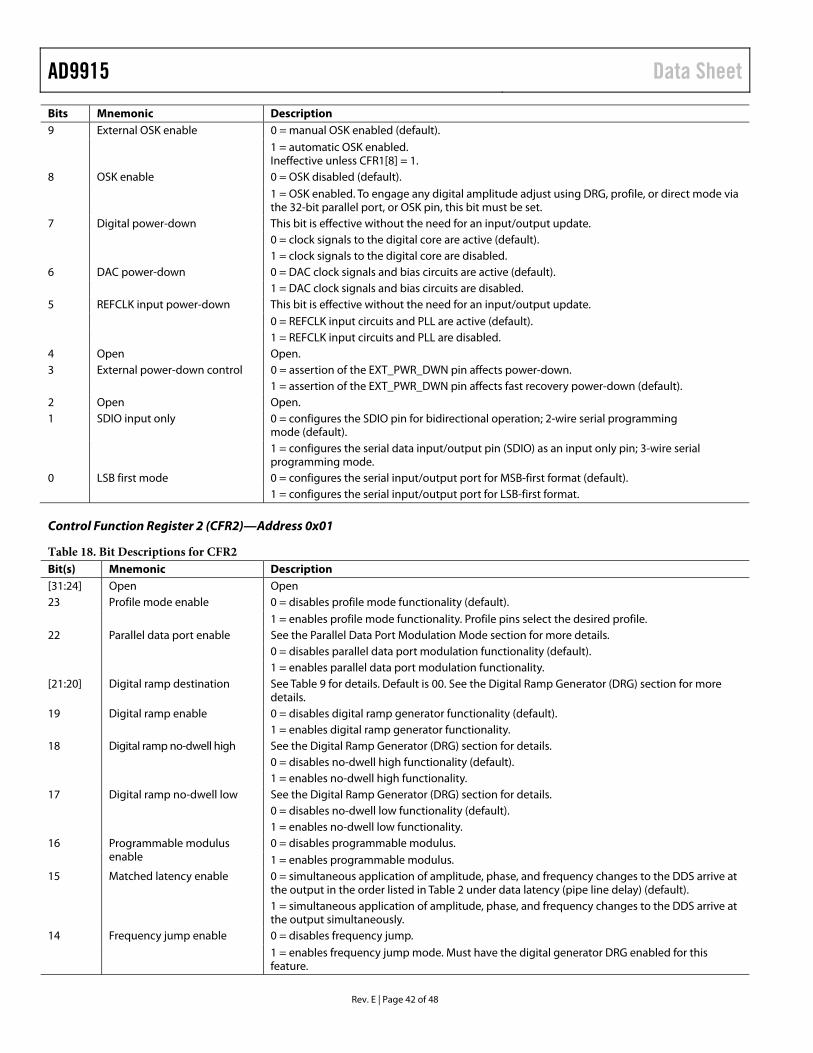
AD9915 Data Sheet
Rev. E | Page 42 of 48
Bits Mnemonic Description 9 External OSK enable 0 = manual OSK enabled (default).
1 = automatic OSK enabled. Ineffective unless CFR1[8] = 1.
8 OSK enable 0 = OSK disabled (default). 1 = OSK enabled. To engage any digital amplitude adjust using DRG, profile, or direct mode via the 32-bit parallel port, or OSK pin, this bit must be set.
7 Digital power-down This bit is effective without the need for an input/output update. 0 = clock signals to the digital core are active (default). 1 = clock signals to the digital core are disabled. 6 DAC power-down 0 = DAC clock signals and bias circuits are active (default). 1 = DAC clock signals and bias circuits are disabled. 5 REFCLK input power-down This bit is effective without the need for an input/output update.
0 = REFCLK input circuits and PLL are active (default). 1 = REFCLK input circuits and PLL are disabled. 4 Open Open. 3 External power-down control 0 = assertion of the EXT_PWR_DWN pin affects power-down. 1 = assertion of the EXT_PWR_DWN pin affects fast recovery power-down (default). 2 Open Open. 1 SDIO input only 0 = configures the SDIO pin for bidirectional operation; 2-wire serial programming
mode (default). 1 = configures the serial data input/output pin (SDIO) as an input only pin; 3-wire serial
programming mode. 0 LSB first mode 0 = configures the serial input/output port for MSB-first format (default). 1 = configures the serial input/output port for LSB-first format.
Control Function Register 2 (CFR2)—Address 0x01
Table 18. Bit Descriptions for CFR2 Bit(s) Mnemonic Description [31:24] Open Open 23 Profile mode enable 0 = disables profile mode functionality (default).
1 = enables profile mode functionality. Profile pins select the desired profile. 22 Parallel data port enable See the Parallel Data Port Modulation Mode section for more details. 0 = disables parallel data port modulation functionality (default). 1 = enables parallel data port modulation functionality. [21:20] Digital ramp destination See Table 9 for details. Default is 00. See the Digital Ramp Generator (DRG) section for more
details. 19 Digital ramp enable 0 = disables digital ramp generator functionality (default). 1 = enables digital ramp generator functionality. 18 Digital ramp no-dwell high See the Digital Ramp Generator (DRG) section for details. 0 = disables no-dwell high functionality (default). 1 = enables no-dwell high functionality. 17 Digital ramp no-dwell low See the Digital Ramp Generator (DRG) section for details. 0 = disables no-dwell low functionality (default). 1 = enables no-dwell low functionality. 16 Programmable modulus
enable 0 = disables programmable modulus. 1 = enables programmable modulus.
15 Matched latency enable 0 = simultaneous application of amplitude, phase, and frequency changes to the DDS arrive at the output in the order listed in Table 2 under data latency (pipe line delay) (default).
1 = simultaneous application of amplitude, phase, and frequency changes to the DDS arrive at the output simultaneously.
14 Frequency jump enable 0 = disables frequency jump.
1 = enables frequency jump mode. Must have the digital generator DRG enabled for this feature.

Data Sheet AD9915
Rev. E | Page 43 of 48
Bit(s) Mnemonic Description 13 DRG over output enable 0 = disables the DROVER output.
1 = enables the DROVER output. 12 Open Open. 11 SYNC_CLK enable 0 = the SYNC_CLK pin is disabled and forced to a static Logic 0 state; the internal clock signal
continues to operate and provide timing to the data assembler. 1 = the internal SYNC_CLK signal appears at the SYNC_CLK pin (default). 10 SYNC_CLK invert 0 = normal SYNC_CLK polarity; Q data associated with Logic 1, I data with Logic 0 (default). 1 = inverted SYNC_CLK polarity. 9 SYNC_OUT enable 0 = the SYNC_OUT pin is disabled; static Logic 0 output.
1 = the SYNC_OUT pin is enabled. 8 SYNC out/in mux enable 0 = the SYNC_OUT signal is routed to the SYNC_OUT pin.
1 = the SYNC_IN signal is routed to the SYNC_OUT pin. [7:0] Open Open.
Control Function Register 3 (CFR3)—Address 0x02
Table 19. Bit Descriptions for CFR3 Bit(s) Mnemonic Description [31:23] Open Open. 22 Input divider reset 0 = disables input divider reset function. 1 = initiates a input divider reset. [21:20] Input divider Divides the input REF CLK signal by one of four values (1, 2, 4, 8). Bit 17 must be set to Logic 1
to enable the PLL input divider. 00 = divide by 1 01 = divide by 2 10 = divide by 4 11 = divide by 8 19 Doubler enable 0 = disables the doubler feature. 1 = enables the doubler feature. Must have the doubler clock edge bit set to Logic 1 to utilize
this feature. 18 PLL enable 0 = disables the internal PLL. 1 = the internal PLL is enabled and the output generates the system clock. The PLL must be
calibrated when enabled via VCO calibration in Register CFR1, Bit 24. 17 PLL input divider enable 0 = disables the PLL input divider function. 1 = enables the PLL input divider function. 16 Doubler clock edge 0 = disables the internal doubler circuit. 1 = enables the doubler circuit. Must have doubler enable bit set to Logic 1 to utilize this
feature. [15:8] Feedback divider N The N divider value in Bits[15:8] is one part of the total PLL multiplication available. The second
part is the fixed divide by two element in the feedback path. Therefore, the total PLL multiplication value is 2N. The valid N divider range is 10× to 255×. The default N value for Bits[15:8] = 25. This sets the total default PLL multiplication to 50× or 2N.
7 Open Open. 6 Manual ICP selection 0 = the internal charge pump current is chosen automatically during the VCO calibration
routine (default). 1 = the internal charge pump is set manually per Table 7.
[5:3] ICP Manual charge pump current selection. See Table 7. 2 Lock detect enable 0 = disables PLL lock detection. 1 = enables PLL lock detection. [1:0] Minimum LDW Selects the number of REF CLK cycles that the phase error (at the PFD inputs) must remain
within before a PLL lock condition can be read back via Bit 24 in Register 0x00. 00 = 128 REF CLK cycles 01 = 256 REF CLK cycles 10 = 512 REF CLK cycles 11 = 1024 REF CLK cycles

AD9915 Data Sheet
Rev. E | Page 44 of 48
Control Function Register 4 (CFR4)—Address 0x03
Table 20. Bit Descriptions for DAC Bit(s) Mnemonic Description [31:27] Open Open. 26 Auxiliary divider power-
down 0 = enables the SYNC OUT circuitry. 1 = disables the SYNC OUT circuitry
25 DAC CAL clock power-down
0 = enables the DAC CAL clock if Bit 26 in Register 0x03 is Logic 0. 1 = disables the DAC CAL clock.
24 DAC CAL enable 1 = initiates an auto DAC calibration. The DAC CAL calibration is required at power-up and any time the internal system clock is changed.
[23:0] (See description) These bits must always be programmed with the default values listed in the default column in Table 16.
Digital Ramp Lower Limit Register—Address 0x04
This register is effective only if the digital ramp enable bit in the CFR2 register (0x01[19]) = 1. See the Digital Ramp Generator (DRG) section for details.
Table 21. Bit Descriptions for Digital Ramp Lower Limit Register Bit(s) Mnemonic Description [31:0] Digital ramp lower limit 32-bit digital ramp lower limit value.
Digital Ramp Upper Limit Register—Address 0x05
This register is effective only if the digital ramp enable bit in the CFR2 register (0x01[19]) = 1. See the Digital Ramp Generator (DRG) section for details.
Table 22. Bit Descriptions for Digital Ramp Limit Register Bit(s) Mnemonic Description [31:0] Digital ramp upper limit 32-bit digital ramp upper limit value.
Rising Digital Ramp Step Size Register—Address 0x06
This register is effective only if the digital ramp enable bit in the CFR2 register (0x01[19]) = 1. See the Digital Ramp Generator (DRG) section for details.
Table 23. Bit Descriptions for Rising Digital Ramp Step Size Register Bit(s) Mnemonic Description [31:0] Rising digital ramp
increment step size 32-bit digital ramp increment step size value.
Falling Digital Ramp Step Size Register—Address 0x07
This register is effective only if the digital ramp enable bit in the CFR2 register (0x01[19]) = 1. See the Digital Ramp Generator (DRG) section for details.
Table 24. Bit Descriptions for Falling Digital Ramp Step Size Register Bit(s) Mnemonic Description [31:0] Falling digital ramp
decrement step size 32-bit digital ramp decrement step size value.

Data Sheet AD9915
Rev. E | Page 45 of 48
Digital Ramp Rate Register—Address 0x08
This register is effective only if the digital ramp enable bit in the CFR2 register (0x01[19]) = 1. See the Digital Ramp Generator (DRG) section for details.
Table 25. Bit Descriptions for Digital Ramp Rate Register Bit(s) Mnemonic Description [31:16] Digital ramp negative slope
rate 16-bit digital ramp negative slope value that defines the time interval between decrement values.
[15:0] Digital ramp positive slope rate
16-bit digital ramp positive slope value that defines the time interval between increment values.
Lower Frequency Jump Register—Address 0x09
This register is effective only if the digital ramp enable bit (0x01[19]) = 1 and the frequency jump enable bit (0x01[14]) = 1 in the CFR2 register. See the Digital Ramp Generator (DRG) section for details.
Table 26. Bit Descriptions for Lower Frequency Jump Register Bit(s) Mnemonic Description [31:0] Lower frequency jump
point 32-bit digital lower frequency jump value. Any time the lower frequency jump value is reached during a frequency sweep, the output frequency jumps to the upper frequency value instantaneously and continues frequency sweeping in a phase-continuous manner.
Upper Frequency Jump Register—Address 0x0A
This register is effective only if the digital ramp enable bit (0x01[19]) = 1 and the frequency jump enable bit (0x01[14]) = 1 in the CFR2 register. See the Digital Ramp Generator (DRG) section for details.
Table 27. Bit Descriptions for Upper Frequency Jump Register Bit(s) Mnemonic Description [31:0] Upper frequency jump
point 32-bit digital upper frequency jump value. Any time the upper frequency jump value is reached during a frequency sweep, the output frequency jumps to the lower frequency value instantaneously and continues frequency sweeping in a phase-continuous manner.

AD9915 Data Sheet
Rev. E | Page 46 of 48
Profile Registers There are 16 serial input/output addresses (Address 0x0B to Address 0x01A) dedicated to device profiles. Eight of the 16 profiles house up to eight single tone frequencies.
The remaining eight profiles contain the corresponding phase offset and amplitude parameters relative to the profile pin setting. To enable profile mode, set the profile mode enable bit in CFR2 (0x01[23]) = 1. The active profile register is selected using the external PS[2:0] pins.
Profile 0 to Profile 7, Single Tone Registers—0x0B, 0x0D, 0x0F, 0x11, 0x13, 0x15, 0x17, 0x19
Four bytes are assigned to each register.
Table 28. Bit Descriptions for Profile 0 to Profile 7 Single Tone Registers Bit(s) Mnemonic Description [31:0] Frequency tuning word This 32-bit number controls the DDS frequency.
Profile 0 to Profile 7, Phase Offset and Amplitude Registers—0x0C, 0x0E, 0x10, 0x12, 0x14, 0x16, 0x18, 0x1A
Four bytes are assigned to each register.
Table 29. Bit Descriptions for Profile 0 to Profile 7 Phase Offset and Amplitude Registers Bit(s) Mnemonic Description [31:28] Open Open. [27:16] Amplitude scale factor This 12-bit word controls the DDS frequency. Note that the OSK enable bit (0x00[8]) must
be set to logic high to make amplitude adjustments. [15:0] Phase offset word This 16-bit word controls the DDS frequency.
USR0 Register—Address 0x1B
Table 30. Bit Descriptions for USR0 Register Bit(s) Mnemonic Description [31:25] Open 24 PLL lock This is a readback bit only. If Logic 1 is read back, the PLL is locked. Logic 0 represents a
nonlocked state. [23:8] (See description) These bits must always be programmed with the default values listed in the default column
in Table 16. 7 Reserved Must be kept at Logic 0 (default). 6 CAL with SYNC 0 = a SYNC_IN signal is not required to calibrate the DAC clock.
1 = a SYNC_IN signal is required to calibrate the DAC clock. [5:3] SYNC_OUT delay ADJ Provides the ability to delay the SYNC_OUT signal for multichip synchronization purposes. [2:0] SYNC_IN delay ADJ Provides the ability to delay the internal SYNC_IN signal for multichip synchronization
purposes.

Data Sheet AD9915
Rev. E | Page 47 of 48
OUTLINE DIMENSIONS
Figure 50. 88-Lead Lead Frame Chip Scale Package [LFCSP_VQ]
12 mm × 12 mm Body, Very Thin Quad (CP-88-5)
Dimensions shown in millimeters
ORDERING GUIDE Parameter1 Temperature Range Package Description Package Option AD9915BCPZ −40°C to +85°C 88-Lead Lead Frame Chip Scale Package [LFCSP_VQ] CP-88-5 AD9915BCPZ-REEL7 −40°C to +85°C 88-Lead Lead Frame Chip Scale Package [LFCSP_VQ] CP-88-5 AD9915/PCBZ Evaluation Board 1 Z = RoHS Compliant Part.
*COMPLIANT TO JEDEC STANDARDS MO-220-VRRDEXCEPT FOR MINIMUM THICKNESS AND LEAD COUNT. 07
-03-
2014
-C
1
22
66
452344
8867
0.500.400.30
0.300.230.18
10.50REF
0.60 MAX0.60MAX
0.50BSC
0.138~0.194 REF
12° MAX
SEATINGPLANE
0.700.650.60 0.045
0.0250.005
PIN 1INDICATOR
12.1012.00 SQ11.90
11.8511.75 SQ11.65
*0.900.850.75
FOR PROPER CONNECTION OFTHE EXPOSED PAD, REFER TOTHE PIN CONFIGURATION ANDFUNCTION DESCRIPTIONSSECTION OF THIS DATA SHEET.COPLANARITY
0.08
6.806.70 SQ6.60
PIN 1INDICATOR
TOP VIEW
EXPOSEDPAD
BOTTOM VIEW
PKG
-004
081

AD9915 Data Sheet
Rev. E | Page 48 of 48
NOTES
©2012–2016 Analog Devices, Inc. All rights reserved. Trademarks and registered trademarks are the property of their respective owners. D10837-0-1/16(E)