AD9910 (Rev. E) - analog.com · AD9910 is a direct digital synthesizer (DDS) featuring an...
64
1 GSPS, 14-Bit, 3.3 V CMOS Direct Digital Synthesizer Data Sheet AD9910 Rev. E Document Feedback Information furnished by Analog Devices is believed to be accurate and reliable. However, no responsibility is assumed by Analog Devices for its use, nor for any infringements of patents or other rights of third parties that may result from its use. Specifications subject to change without notice. No license is granted by implication or otherwise under any patent or patent rights of Analog Devices. Trademarks and registered trademarks are the property of their respective owners. One Technology Way, P.O. Box 9106, Norwood, MA 02062-9106, U.S.A. Tel: 781.329.4700 ©2007–2016 Analog Devices, Inc. All rights reserved. Technical Support www.analog.com FEATURES 1 GSPS internal clock speed (up to 400 MHz analog output) Integrated 1 GSPS, 14-bit DAC 0.23 Hz or better frequency resolution Phase noise ≤ −125 dBc/Hz @ 1 kHz offset (400 MHz carrier) Excellent dynamic performance with >80 dB narrow-band SFDR Serial input/output (I/O) control Automatic linear or arbitrary frequency, phase, and amplitude sweep capability 8 frequency and phase offset profiles Sin(x)/(x) correction (inverse sinc filter) 1.8 V and 3.3 V power supplies Software and hardware controlled power-down 100-lead TQFP_EP package Integrated 1024 word × 32-bit RAM PLL REFCLK multiplier Parallel datapath interface Internal oscillator can be driven by a single crystal Phase modulation capability Amplitude modulation capability Multichip synchronization APPLICATIONS Agile local oscillator (LO) frequency synthesis Programmable clock generators FM chirp source for radar and scanning systems Test and measurement equipment Acousto-optic device drivers Polar modulators Fast frequency hopping FUNCTIONAL BLOCK DIAGRAM 14-BIT DAC 1GSPS DDS CORE LINEAR RAMP GENERATOR 1024- ELEMENT RAM HIGH SPEED PARALLEL DATA INTERFACE TIMING AND CONTROL SERIAL CONTROL DATA PORT REFCLK MULTIPLIER 06479-001 AD9910 Figure 1.
Transcript of AD9910 (Rev. E) - analog.com · AD9910 is a direct digital synthesizer (DDS) featuring an...

1 GSPS, 14-Bit, 3.3 V CMOSDirect Digital Synthesizer
Data Sheet AD9910
Rev. E Document Feedback Information furnished by Analog Devices is believed to be accurate and reliable. However, no responsibility is assumed by Analog Devices for its use, nor for any infringements of patents or other rights of third parties that may result from its use. Specifications subject to change without notice. No license is granted by implication or otherwise under any patent or patent rights of Analog Devices. Trademarks and registered trademarks are the property of their respective owners.
One Technology Way, P.O. Box 9106, Norwood, MA 02062-9106, U.S.A.Tel: 781.329.4700 ©2007–2016 Analog Devices, Inc. All rights reserved. Technical Support www.analog.com
FEATURES 1 GSPS internal clock speed (up to 400 MHz analog output) Integrated 1 GSPS, 14-bit DAC 0.23 Hz or better frequency resolution Phase noise ≤ −125 dBc/Hz @ 1 kHz offset (400 MHz carrier) Excellent dynamic performance with
>80 dB narrow-band SFDR Serial input/output (I/O) control Automatic linear or arbitrary frequency, phase, and
amplitude sweep capability 8 frequency and phase offset profiles Sin(x)/(x) correction (inverse sinc filter) 1.8 V and 3.3 V power supplies Software and hardware controlled power-down 100-lead TQFP_EP package Integrated 1024 word × 32-bit RAM PLL REFCLK multiplier Parallel datapath interface Internal oscillator can be driven by a single crystal Phase modulation capability Amplitude modulation capability Multichip synchronization
APPLICATIONS Agile local oscillator (LO) frequency synthesis Programmable clock generators FM chirp source for radar and scanning systems Test and measurement equipment Acousto-optic device drivers Polar modulators Fast frequency hopping
FUNCTIONAL BLOCK DIAGRAM
14-BIT DAC1GSPS DDS CORE
LINEARRAMP
GENERATOR
1024-ELEMENT
RAM
HIGH SPEED PARALLELDATA INTERFACE
TIMING AND CONTROL
SERIAL CONTROLDATA PORT
REFCLKMULTIPLIER
0647
9-00
1AD9910
Figure 1.

AD9910 Data Sheet
Rev. E | Page 2 of 64
TABLE OF CONTENTS Features .............................................................................................. 1
Applications ....................................................................................... 1
Functional Block Diagram .............................................................. 1
Revision History ............................................................................... 3
General Description ......................................................................... 4
Specifications ..................................................................................... 5
Electrical Specifications ............................................................... 5
Absolute Maximum Ratings ............................................................ 8
Equivalent Circuits ....................................................................... 8
ESD Caution .................................................................................. 8
Pin Configuration and Function Descriptions ............................. 9
Typical Performance Characteristics ........................................... 12
Application Circuits ....................................................................... 15
Theory of Operation ...................................................................... 16
Single Tone Mode ....................................................................... 16
RAM Modulation Mode ............................................................ 17
Digital Ramp Modulation Mode .............................................. 18
Parallel Data Port Modulation Mode ....................................... 19
Mode Priority .............................................................................. 21
Functional Block Detail ................................................................. 22
DDS Core ..................................................................................... 22
14-Bit DAC Output .................................................................... 22
Inverse Sinc Filter ....................................................................... 23
Clock Input (REF_CLK/REF_CLK) ........................................ 23
PLL Lock Indication ................................................................... 26
Output Shift Keying (OSK) ....................................................... 26
Digital Ramp Generator (DRG) ............................................... 27
RAM Control .............................................................................. 32
Additional Features ........................................................................ 41
Profiles ......................................................................................... 41
I/O_UPDATE, SYNC_CLK, and System Clock Relationships....................................................................................................... 41
Automatic I/O Update ............................................................... 42
Power-Down Control ................................................................ 42
Synchronization of Multiple Devices ........................................... 43
Power Supply Partitioning ............................................................. 46
3.3 V Supplies .............................................................................. 46
1.8 V Supplies .............................................................................. 46
Serial Programming ....................................................................... 47
Control Interface—Serial I/O ................................................... 47
General Serial I/O Operation ................................................... 47
Instruction Byte .......................................................................... 47
Serial I/O Port Pin Descriptions .............................................. 47
Serial I/O Timing Diagrams ..................................................... 48
MSB/LSB Transfers .................................................................... 48
Register Map and Bit Descriptions .............................................. 49
Register Bit Descriptions ........................................................... 54
Outline Dimensions ....................................................................... 61
Ordering Guide .......................................................................... 61

Data Sheet AD9910
Rev. E | Page 3 of 64
REVISION HISTORY 10/2016—Rev. D to Rev. E Change to Figure 33 ........................................................................ 25 5/2012—Rev. C to Rev. D Changes to Table 1 ............................................................................ 8 Changes to Table 3 .......................................................................... 12 Changes to Figure 39 ...................................................................... 31 Changes to Synchronization of Multiple Devices Section ......... 45 Changes to Table 18 ........................................................................ 55 Changes to Table 20 ........................................................................ 58 Changes to Table 26 ........................................................................ 60 8/2010—Rev. B to Rev. C Changes to XTAL_SEL Input Parameter in Table 1 ..................... 8 Changes to Table 2 ............................................................................ 9 Changes to Transmit Enable (TxENABLE) Section ................... 21 12/2008—Rev. A to Rev. B Changes to Figure 2........................................................................... 5 Changes to I/O_UPDATE Pulse Width Parameter and Minimum Profile Toggle Period Parameter in Table 1 ................ 7 Added XTAL_SEL Input Parameter in Table 1 ............................. 8 Changes to Table 3 .......................................................................... 11 Changes to Figure 20 ...................................................................... 16 Changes to Figure 22 ...................................................................... 17 Changes to Figure 23 ...................................................................... 18 Changes to Figure 24 ...................................................................... 19 Changes to Figure 25 ...................................................................... 20 Changes to REF_CLK/REF_CLK Overview Section ................. 24 Changes to Crystal Driven REF_CLK/REF_CLK Section ........ 25 Changes to PLL Lock Indication Section and Output Shift Keying (OSK) Section ..................................................................... 27 Changes to DRG Slope Control Section and Normal Ramp Generation Section.......................................................................... 30 Changes to Drover Pin Section ..................................................... 32 Changes to Figure 43 ...................................................................... 35 Changes to Figure 45 and Internal Profile Control Continuous Waveform Timing Diagram Section ............................................. 38 Changes to Figure 47 ...................................................................... 40
Changes to Figure 48 ...................................................................... 41 Deleted I/O_UPDATE Pin Section .............................................. 41 Changes to Profiles Section ........................................................... 42 Added I/O_UPDATE, SYNC_CLK, and System Clock Relationships Section ...................................................................... 42 Added Figure 49; Renumbered Sequentially ............................... 42 Changes to Synchronization of Multiple Devices Section ......... 44 Changes to DVDD (1.8V) (Pin 17, Pin 23, Pin 30, Pin 47, Pin 57, and Pin 64) Section and AVDD (1.8V) (Pin 89 and Pin 92) Section................................................................................. 47 Changes to Control Interface—Serial I/O Section ..................... 48 Changes to Table 17 ........................................................................ 50 Changes to Table 19 ........................................................................ 57 Changes to Table 20 and Table 21 ................................................. 58 2/2008—Rev. 0 to Rev. A Changes to Features .......................................................................... 1 Changes to REFCLK Multiplier Specification in Table 1 ............ 5 Changes to Minimum Setup Time to SYNC_CLK....................... 6 Changes to I/O Update/Profile[2:0] Timing Characteristics ...... 6 Changes to TxENABLE/Data Setup Time (to PDCLK) and TxENABLE/Data Hold Time (to PDCLK) .................................... 6 Changes to Miscellaneous Timing Characteristics....................... 6 Changes to Table 3 .......................................................................... 10 Changes to Figure 9, Figure 10, Figure 11, Figure 12, Figure 13, and Figure 14 ................................................................................... 12 Changes to Figure 30 and Table 7 ................................................. 24 Changes to Automatic I/O Update Section ................................. 41 Added Table 16, Renumbered Sequentially ................................. 41 Changes to Figure 49 to Figure 53 ................................................ 43 Added Power Supply Partitioning Section .................................. 46 Changes to General Serial I/O Operation Section ..................... 47 Changes to Table 17 ........................................................................ 49 Changes to Table 19 ........................................................................ 56 Changes to Table 20 ........................................................................ 57 Added Table 32 ................................................................................ 60 5/2007—Revision 0: Initial Version

AD9910 Data Sheet
Rev. E | Page 4 of 64
GENERAL DESCRIPTION The AD9910 is a direct digital synthesizer (DDS) featuring an integrated 14-bit DAC and supporting sample rates up to 1 GSPS. The AD9910 employs an advanced, proprietary DDS technology that provides a significant reduction in power con-sumption without sacrificing performance. The DDS/DAC combination forms a digitally programmable, high frequency, analog output synthesizer capable of generating a frequency agile sinusoidal waveform at frequencies up to 400 MHz.
The user has access to the three signal control parameters that control the DDS: frequency, phase, and amplitude. The DDS provides fast frequency hopping and frequency tuning resolu-tion with its 32-bit accumulator. With a 1 GSPS sample rate, the tuning resolution is ~0.23 Hz. The DDS also enables fast phase and amplitude switching capability.
The AD9910 is controlled by programming its internal control registers via a serial I/O port. The AD9910 includes an integrated static RAM to support various combinations of frequency, phase, and/or amplitude modulation. The AD9910 also supports a user defined, digitally controlled, digital ramp mode of operation. In this mode, the frequency, phase, or amplitude can be varied linearly over time. For more advanced modulation functions, a high speed parallel data input port is included to enable direct frequency, phase, amplitude, or polar modulation.
The AD9910 is specified to operate over the extended industrial temperature range (see the Absolute Maximum Ratings section for details).
0647
9-00
2
16PARALLEL
INPUT
PDCLK
SCLK
SDIO
I/O_RESET
PROFILE[2:0]
I/O_UPDATE
RAM
POWER-DOWN
CONTROL
EXT_
PWR
_DW
N
DAC_RSET
IOUT
IOUT
CS
TxENABLE
DAC FSC
OSK
RAM_SWP_OVR
A
θ INVERSESINC
FILTER
CLOCK
AMPLITUDE (A)
FREQUENCY (ω)
PHASE (θ)
DIGITALRAMP
GENERATOR
8
DAC FSC8
2DRCTLDRHOLD
DROVER
2
MULTICHIPSYNCHRONIZATION
SYSCLK
PLL
÷2
CLO
CK
MO
DE
REF_CLK
REF_CLK
REFCLK_OUT
XTAL_SELPARALLEL DATA
TIMING ANDCONTROL
SER
IAL
I/O P
OR
T2 AD9910
PROGRAMMINGREGISTERS
OUTPUTSHIFT
KEYING
DATAROUTE
ANDPARTITIONCONTROL
3
INTERNAL CLOCK TIMINGAND CONTROL
ω
Acos (ωt + θ)
Asin (ωt + θ)
SYN
C_S
MP_
ERR
SYN
C_C
LK
SYN
C_O
UT
SYN
C_I
N
PLL_
LOC
K
PLL_
LOO
P_FI
LTER
MA
STER
_RES
ET
22
DAC14-BIT
DDS
AUXDAC8-BIT
Figure 2. Detailed Block Diagram

Data Sheet AD9910
Rev. E | Page 5 of 64
SPECIFICATIONS ELECTRICAL SPECIFICATIONS AVDD (1.8 V) and DVDD (1.8 V) = 1.8 V ± 5%, AVDD (3.3 V) = 3.3 V ± 5%, DVDD_I/O (3.3 V) = 3.3 V ± 5%, T = 25°C, RSET = 10 kΩ, IOUT = 20 mA, external reference clock frequency = 1000 MHz with reference clock (REFCLK) multiplier disabled, unless otherwise noted.
Table 1. Parameter Conditions/Comments Min Typ Max Unit REFCLK INPUT CHARACTERISTICS
Frequency Range REFCLK Multiplier Disabled 60 1000 MHz Enabled 3.2 60 MHz Maximum REFCLK Input Divider Frequency Full temperature range 1500 1900 MHz Minimum REFCLK Input Divider Frequency Full temperature range 25 35 MHz
External Crystal 25 MHz Input Capacitance 3 pF Input Impedance Differential 2.8 kΩ Single-ended 1.4 kΩ Duty Cycle REFCLK multiplier disabled 45 55 % REFCLK multiplier enabled 40 60 % REFCLK Input Level Single-ended 50 1000 mV p-p Differential 100 2000 mV p-p
REFCLK MULTIPLIER VCO CHARACTERISTICS VCO Gain (KV) @ Center Frequency VCO range Setting 0 429 MHz/V
VCO range Setting 1 500 MHz/V VCO range Setting 2 555 MHz/V VCO range Setting 3 750 MHz/V VCO range Setting 4 789 MHz/V VCO range Setting 51 850 MHz/V REFCLK_OUT CHARACTERISTICS
Maximum Capacitive Load 20 pF Maximum Frequency 25 MHz
DAC OUTPUT CHARACTERISTICS Full-Scale Output Current 8.6 20 31.6 mA Gain Error −10 +10 % FS Output Offset 2.3 µA Differential Nonlinearity 0.8 LSB Integral Nonlinearity 1.5 LSB Output Capacitance 5 pF Residual Phase Noise @ 1 kHz offset, 20 MHz AOUT
REFCLK Multiplier Disabled −152 dBc/Hz Enabled @ 20× −140 dBc/Hz Enabled @ 100× −140 dBc/Hz
Voltage Compliance Range −0.5 +0.5 V Wideband SFDR See the Typical Performance
Characteristics section
Narrow-Band SFDR 50.1 MHz Analog Output ±500 kHz –87 dBc ±125 kHz –87 dBc ±12.5 kHz –96 dBc 101.3 MHz Analog Output ±500 kHz –87 dBc ±125 kHz –87 dBc ±12.5 kHz –95 dBc

AD9910 Data Sheet
Rev. E | Page 6 of 64
Parameter Conditions/Comments Min Typ Max Unit 201.1 MHz Analog Output ±500 kHz –87 dBc ±125 kHz –87 dBc ±12.5 kHz –91 dBc 301.1 MHz Analog Output ±500 kHz –86 dBc ±125 kHz –86 dBc ±12.5 kHz –88 dBc 401.3 MHz Analog Output ±500 kHz –84 dBc ±125 kHz –84 dBc ±12.5 kHz –85 dBc
SERIAL PORT TIMING CHARACTERISTICS Maximum SCLK Frequency 70 Mbps Minimum SCLK Clock Pulse Width Low 4 ns
High 4 ns Maximum SCLK Rise/Fall Time 2 ns Minimum Data Setup Time to SCLK 5 ns Minimum Data Hold Time to SCLK 0 ns Maximum Data Valid Time in Read Mode 11 ns
I/O_UPDATE/PROFILE[2:0] TIMING CHARACTERISTICS
Minimum Setup Time to SYNC_CLK 1.75 ns Minimum Hold Time to SYNC_CLK 0 ns I/O_UPDATE Pulse Width High >1 SYNC_CLK cycle Minimum Profile Toggle Period 2 SYNC_CLK cycles
TxENABLE and 16-BIT PARALLEL (DATA) BUS TIMING Maximum PDCLK Frequency 250 MHz TxENABLE/Data Setup Time (to PDCLK) 1.75 ns TxENABLE/Data Hold Time (to PDCLK) 0 ns
MISCELLANEOUS TIMING CHARACTERISTICS Wake-Up Time2
Fast Recovery 8 SYSCLK cycles3 Full Sleep Mode REFCLK multiplier enabled 1 ms REFCLK multiplier disabled 150 μs
Minimum Reset Pulse Width High 5 SYSCLK cycles3 DATA LATENCY (PIPELINE DELAY)
Data Latency, Single Tone or Using Profiles Frequency, Phase, Amplitude-to-DAC Output Matched latency enabled and OSK
enabled 91 SYSCLK cycles3
Frequency, Phase-to-DAC Output Matched latency enabled and OSK disabled
79 SYSCLK cycles3
Matched latency disabled 79 SYSCLK cycles3 Amplitude-to-DAC Output Matched latency disabled 47 SYSCLK cycles3
Data Latency Using RAM Mode Frequency, Phase-to-DAC Output Matched latency enabled/disabled 94 SYSCLK cycles3 Amplitude-to-DAC Output Matched latency enabled 106 SYSCLK cycles3 Matched latency disabled 58 SYSCLK cycles3
Data Latency, Sweep Mode Frequency, Phase-to-DAC Output Matched latency enabled/disabled 91 SYSCLK cycles3 Amplitude-to-DAC Output Matched latency enabled 91 SYSCLK cycles3 Matched latency disabled 47 SYSCLK cycles3
Data Latency, 16-Bit Input Modulation Mode Frequency, Phase-to-DAC Output Matched latency enabled 103 SYSCLK cycles3 Matched latency disabled 91 SYSCLK cycles3

Data Sheet AD9910
Rev. E | Page 7 of 64
Parameter Conditions/Comments Min Typ Max Unit CMOS LOGIC INPUTS
Logic 1 Voltage 2.0 V Logic 0 Voltage 0.8 V Logic 1 Current 90 150 µA Logic 0 Current 90 150 µA Input Capacitance 2 pF
XTAL_SEL INPUT Logic 1 Voltage 1.25 V Logic 0 Voltage 0.6 V Input Capacitance 2 pF
CMOS LOGIC OUTPUTS 1 mA load Logic 1 Voltage 2.8 V Logic 0 Voltage 0.4 V
POWER SUPPLY CURRENT IAVDD (1.8 V) 110 mA IAVDD (3.3 V) 29 mA IDVDD (1.8 V) 222 mA IDVDD (3.3 V) 11 mA
TOTAL POWER CONSUMPTION Single Tone Mode 715 950 mW Rapid Power-Down Mode 330 450 mW Full Sleep Mode 19 40 mW
1 The gain value for VCO range Setting 5 is measured at 1000 MHz. 2 Wake-up time refers to the recovery time from a power-down state. The longest time required is for the reference clock multiplier PLL to relock to the reference. The
wake-up time assumes that the recommended PLL loop filter values are used. 3 SYSCLK cycle refers to the actual clock frequency used on-chip by the DDS. If the reference clock multiplier is used to multiply the external reference clock frequency,
the SYSCLK frequency is the external frequency multiplied by the reference clock multiplication factor. If the reference clock multiplier is not used, the SYSCLK frequency is the same as the external reference clock frequency.

AD9910 Data Sheet
Rev. E | Page 8 of 64
ABSOLUTE MAXIMUM RATINGS Table 2. Parameter Rating AVDD (1.8V), DVDD (1.8V) Supplies 2 V AVDD (3.3V), DVDD_I/O (3.3V) Supplies 4 V Digital Input Voltage −0.7 V to +4 V XTAL_SEL −0.7 V TO +2.2 V Digital Output Current 5 mA Storage Temperature Range −65°C to +150°C Operating Temperature Range −40°C to +85°C θJA 22°C/W
θJC 2.8°C/W
Maximum Junction Temperature 150°C Lead Temperature (10 sec Soldering) 300°C
Stresses at or above those listed under Absolute Maximum Ratings may cause permanent damage to the product. This is a stress rating only; functional operation of the product at these or any other conditions above those indicated in the operational section of this specification is not implied. Operation beyond the maximum operating conditions for extended periods may affect product reliability.
EQUIVALENT CIRCUITS
0647
9-00
3
MUST TERMINATE OUTPUTS TO AGNDFOR CURRENT FLOW. DO NOT EXCEEDTHE OUTPUT VOLTAGE COMPLIANCERATING.
IOUT IOUT
DAC OUTPUTSAVDD
Figure 3. Equivalent Input Circuit
AVOID OVERDRIVING DIGITAL INPUTS.FORWARD BIASING ESD DIODES MAYCOUPLE DIGITAL NOISE ONTO POWERPINS.
DIGITAL INPUTS
INPUT
DVDD_I/O
0647
9-05
5
Figure 4. Equivalent Output Circuit
ESD CAUTION

Data Sheet AD9910
Rev. E | Page 9 of 64
PIN CONFIGURATION AND FUNCTION DESCRIPTIONS
26 27 28 29 30
5554535251
TQFP-100 (E_PAD)TOP VIEW
(Not to Scale)
AD9910
D14
D13
DVD
D_I
/O (3
.3V)
DG
ND
DVD
D (1
.8V)
5432
76
98
1
1110
16151413
1817
2019
2221
12
2423
25
32 33 34 35 36 38 39 40 41 42 43 44 45 46 47 48 49 5031 37
D12 D11
D10 D
9D
8D
7D
6D
5D
4PD
CLK
TxEN
AB
LE
DG
NDD3
D2
D1
DVD
D_I
/O (3
.3V)
DVD
D (1
.8V) D0 F1 F0
80IO
UT
79A
GN
D78
AG
ND
77AV
DD
(3.3
V)76
AVD
D (3
.3V)
75 AVDD (3.3V)74 AVDD (3.3V)73 AGND72 NC71 I/O_RESET70 CS69 SCLK68 SDO67 SDIO66 DVDD_I/O (3.3V)65 DGND64 DVDD (1.8V)63 DRHOLD62 DRCTL61 DROVER60 OSK59 I/O_UPDATE58 DGND57 DVDD (1.8V)56 DVDD_I/O (3.3V)
SYNC_CLKPROFILE0PROFILE1PROFILE2DGND
100
99 98 97 96 95 94 93 92 91 90 89 88 87 86 85 84 83 82 81
NC
NC
NC
NC
AG
ND
XTA
L_SE
LR
EFC
LK_O
UT
NC
AVD
D (1
.8V)
REF
_CLK
REF
_CLK
AVD
D (1
.8V)
AG
ND
NC
NC
AG
ND
DA
C_R
SET
AVD
D (3
.3V)
AG
ND
IOU
T
NCPLL_LOOP_FILTER
AVDD (1.8V)AGNDAGND
AVDD (1.8V)SYNC_IN+SYNC_IN–
SYNC_OUT+SYNC_OUT–
DVDD_I/O (3.3V)SYNC_SMP_ERR
DGNDMASTER_RESETDVDD_I/O (3.3V)
DGNDDVDD (1.8V)
EXT_PWR_DWNPLL_LOCK
NCDVDD_I/O (3.3V)
DGNDDVDD (1.8V)
RAM_SWP_OVRD15
0647
9-00
4
PIN 1INDICATOR
NOTES:1. EXPOSED PAD SHOULD BE SOLDERED TO GROUND.2. NC = NO CONNECT.
Figure 5. Pin Configuration

AD9910 Data Sheet
Rev. E | Page 10 of 64
Table 3. Pin Function Descriptions Pin No. Mnemonic I/O1 Description 1, 20, 72, 86, 87, 93, 97 to 100
NC Not Connected. Allow device pins to float.
2 PLL_LOOP_FILTER I PLL Loop Filter Compensation Pin. See the External PLL Loop Filter Components section for details.
3, 6, 89, 92 AVDD (1.8V) I Analog Core VDD, 1.8 V Analog Supplies. 74 to 77, 83 AVDD (3.3V) I Analog DAC VDD, 3.3 V Analog Supplies. 17, 23, 30, 47, 57, 64
DVDD (1.8V) I Digital Core VDD, 1.8 V Digital Supplies.
11, 15, 21, 28, 45, 56, 66
DVDD_I/O (3.3V) I Digital Input/Output VDD, 3.3 V Digital Supplies.
4, 5, 73, 78, 79, 82, 85, 88, 96
AGND I Analog Ground.
13, 16, 22, 29, 46, 51, 58, 65
DGND I Digital Ground.
7 SYNC_IN+ I Synchronization Signal (LVDS), Digital Input (Rising Edge Active). The synchronization signal from the external master to synchronize internal subclocks. See the Synchronization of Multiple Devices section for details.
8 SYNC_IN− I Synchronization Signal (LVDS), Digital Input. The synchronization signal from the external master to synchronize internal subclocks. See the Synchronization of Multiple Devices section for details.
9 SYNC_OUT+ O Synchronization Signal (LVDS), Digital Output (Rising Edge Active). The synchronization signal from the internal device subclocks to synchronize external slave devices. See the Synchronization of Multiple Devices section for details.
10 SYNC_OUT− O Synchronization Signal (LVDS), Digital Output. The synchronization signal from the internal device subclocks to synchronize external slave devices. See the Synchronization of Multiple Devices section for details.
12 SYNC_SMP_ERR O Synchronization Sample Error, Digital Output (Active High). Sync sample error: a high on this pin indicates that the AD9910 did not receive a valid sync signal on SYNC_IN+/SYNC_IN−.
14 MASTER_RESET I Master Reset, Digital Input (Active High). Master reset: clears all memory elements and sets registers to default values.
18 EXT_PWR_DWN I External Power-Down, Digital Input (Active High). A high level on this pin initiates the currently programmed power-down mode. See the Power-Down Control section for further details. If unused, connect to ground.
19 PLL_LOCK O Clock Multiplier PLL Lock, Digital Output (Active High). A high on this pin indicates that the Clock Multiplier PLL has acquired lock to the reference clock input.
24 RAM_SWP_OVR O RAM Sweep Over, Digital Output (Active High). A high on this pin indicates that the RAM sweep profile has completed.
25 to 27, 31 to 39, 42 to 44, 48
D[15:0] I Parallel Input Bus (Active High).
49, 50 F[1:0] I Modulation Format Pins. Digital input to determine the modulation format. 40 PDCLK O Parallel Data Clock. This is the digital output (clock). The parallel data clock provides a
timing signal for aligning data at the parallel inputs. 41 TxENABLE I Transmit Enable. Digital input (active high). In burst mode communications, a high on this
pin indicates new data for transmission. In continuous mode, this pin remains high. 52 to 54 PROFILE[2:0] I Profile Select Pins. Digital inputs (active high). Use these pins to select one of eight
phase/frequency profiles for the DDS. Changing the state of one of these pins transfers the current contents of all I/O buffers to the corresponding registers. State changes should be set up on the SYNC_CLK pin.
55 SYNC_CLK O Output Clock Divided-By-Four. A digital output (clock). Many of the digital inputs on the chip, such as I/O_UPDATE and PROFILE[2:0], need to be set up on the rising edge of this signal.

Data Sheet AD9910
Rev. E | Page 11 of 64
Pin No. Mnemonic I/O1 Description 59 I/O_UPDATE I/O Input/Output Update. Digital input (active high). A high on this pin transfers the contents
of the I/O buffers to the corresponding internal registers. 60 OSK I Output Shift Keying. Digital input (active high). When the OSK features are placed in either
manual or automatic mode, this pin controls the OSK function. In manual mode, it toggles the multiplier between 0 (low) and the programmed amplitude scale factor (high). In automatic mode, a low sweeps the amplitude down to zero, a high sweeps the amplitude up to the amplitude scale factor.
61 DROVER O Digital Ramp Over. Digital output (active high). This pin switches to Logic 1 whenever the digital ramp generator reaches its programmed upper or lower limit.
62 DRCTL I Digital Ramp Control. Digital input (active high). This pin controls the slope polarity of the digital ramp generator. See the Digital Ramp Generator (DRG) section for more details. If not using the digital ramp generator, connect this pin to Logic 0.
63 DRHOLD I Digital Ramp Hold. Digital input (active high). This pin stalls the digital ramp generator in its present state. See the Digital Ramp Generator (DRG) section for more details. If not using a digital ramp generator, connect this pin to Logic 0.
67 SDIO I/O Serial Data Input/Output. Digital input/output (active high). This pin can be either unidirec-tional or bidirectional (default), depending on the configuration settings. In bidirectional serial port mode, this pin acts as the serial data input and output. In unidirectional mode, it is an input only.
68 SDO O Serial Data Output. Digital output (active high). This pin is only active in unidirectional serial data mode. In this mode, it functions as the output. In bidirectional mode, this pin is not operational and should be left floating.
69 SCLK I Serial Data Clock. Digital clock (rising edge on write, falling edge on read). This pin provides the serial data clock for the control data path. Write operations to the AD9910 use the rising edge. Readback operations from the AD9910 use the falling edge.
70 CS I Chip Select. Digital input (active low). This pin allows the AD9910 to operate on a common serial bus for the control data path. Bringing this pin low enables the AD9910 to detect serial clock rising/falling edges. Bringing this pin high causes the AD9910 to ignore input on the serial data pins.
71 I/O_RESET I Input/Output Reset. Digital input (active high). This pin can be used when a serial I/O communication cycle fails (see the I/O_RESET—Input/Output Reset section for details). When not used, connect this pin to ground.
80 IOUT O Open-Drain DAC Complementary Output Source. Analog output (current mode). Connect through a 50 Ω resistor to AGND.
81 IOUT O Open-Drain DAC Output Source. Analog output (current mode). Connect through a 50 Ω resistor to AGND.
84 DAC_RSET O Analog Reference Pin. This pin programs the DAC output full-scale reference current. Attach a 10 kΩ resistor to AGND.
90 REF_CLK I Reference Clock Input. Analog input. When the internal oscillator is engaged, this pin can be driven by either an external oscillator or connected to a crystal. See the REF_CLK/ Overview section for more details.
91 REF_CLK I Reference Clock Input. Analog input. See the REF_CLK/ Overview section for more details.
94 REFCLK_OUT O Crystal Output. Analog output. See the REF_CLK/ Overview section for more details. 95 XTAL_SEL I Crystal Select (1.8 V Logic). Analog input (active high). Driving the XTAL_SEL pin high,
the AVDD (1.8V) pin enables the internal oscillator to be used with a crystal resonator. If unused, connect it to AGND.
EPAD Exposed Paddle (EPAD)
The EPAD should be soldered to ground.
1 I = input, O = output.

AD9910 Data Sheet
Rev. E | Page 12 of 64
TYPICAL PERFORMANCE CHARACTERISTICS –50
–55
–60
–65
–75
–70
0647
9-03
4
SFD
R (d
Bc)
OUTPUT FREQUENCY (MHz)
SFDR WITHOUT PLL
SFDR WITH PLL
0 50 100 150 200 250 300 350 400
Figure 6. Wideband SFDR vs. Output Frequency (PLL with Reference Clock = 15.625 MHz × 64)
400 450300250 350200150100500
0647
9-04
6
SFD
R (d
Bc)
OUTPUT FREQUENCY (MHz)
–75
–70
–65
–60
–55
–45
–50
LOW SUPPLY
HIGH SUPPLY
Figure 7. Wideband SFDR vs. Output Frequency and Supply (±5%), REFCLK = 1 GHz
400 450300250 350200150100500
0647
9-04
7
SFD
R (d
Bc)
OUTPUT FREQUENCY (MHz)
–75
–70
–65
–60
–55
–50
–40°C
+85°C
Figure 8. Wideband SFDR vs. Output Frequency and Temperature, REFCLK = 1 GHz
START 0Hz–100
–90
–80
–70
–60
–50
–40
–30
–20
–10
0
50MHz/DIV STOP 500MHz
0647
9-03
5
1
SFD
R (d
Bc)
Figure 9. Wideband SFDR at 10 MHz, REFCLK = 1 GHz
0
–100
–90
–80
–70
–60
–50
–40
–30
–20
–10
START 0Hz 50MHz/DIV STOP 500MHz
0647
9-03
6
1
SFD
R (d
Bc)
Figure 10. Wideband SFDR at 204 MHz, REFCLK = 1 GHz
0647
9-03
7
START 0Hz–100
–90
–80
–70
–60
–50
–40
–30
–20
–10
0
50MHz/DIV STOP 500MHz
1
SFD
R (d
Bc)
Figure 11. Wideband SFDR at 403 MHz, REFCLK = 1 GHz

Data Sheet AD9910
Rev. E | Page 13 of 64
0647
9-03
8
CENTER 10.32MHz–120
–108
–96
–84
–72
–60
–48
–36
–24
–12
0
2.5kHz/DIV SPAN 25kHz
1
SFD
R (d
Bc)
Figure 12. Narrow-Band SFDR at 10.32 MHz, REFCLK = 1 GHz
0647
9-03
9
CENTER 204.36MHz–120
–108
–96
–84
–72
–60
–48
–36
–24
–12
0
2.5kHz/DIV SPAN 25kHz
1
SFD
R (d
Bc)
Figure 13. Narrow-Band SFDR at 204.36 MHz, REFCLK = 1 GHz
0647
9-04
0
CENTER 403.78MHz–120
–108
–96
–84
–72
–60
–48
–36
–24
–12
0
2.5kHz/DIV SPAN 25kHz
1
SFD
R (d
Bc)
Figure 14. Narrow-Band SFDR at 403.78 MHz, REFCLK = 1 GHz
–90
–100
–120
–110
–140
–150
–130
–170
–160
10 100 1k 10k 100k 100M1M 10M
0647
9-04
2
MA
GN
ITU
DE
(dB
c/H
z)
FREQUENCY OFFSET (Hz)
fOUT = 20.1MHz
fOUT = 98.6MHz
fOUT = 201.1MHz
fOUT = 397.8MHz
Figure 15. Residual Phase Noise Plot, 1 GHz Operation with PLL Disabled

AD9910 Data Sheet
Rev. E | Page 14 of 64
–90
–100
–110
–120
–130
–140
–150
–16010 100 1k 10k 100k 1M 10M 100M
0647
9-04
3
MA
GN
ITU
DE
(dB
c/ H
z)
FREQUENCY OFFSET (Hz)
fOUT = 20.1MHz
fOUT = 397.8MHz
fOUT = 98.6MHz
fOUT = 201.1MHz
Figure 16. Residual Phase Noise,
1 GHz Operation Using a 50 MHz Reference Clock with 20× PLL Multiplier
400
450
300
250
350
200
150
100
50
0100 200 300 400 500 600 700 800 900 1000
0647
9-04
4
POW
ER D
ISSI
PATI
ON
(mW
)
SYSTEM CLOCK FREQUENCY (MHz)
DVDD 3.3V
AVDD 3.3V
AVDD 1.8V
DVDD 1.8V
Figure 17. Power Dissipation vs. System Clock Frequency (PLL Disabled)
400
450
300
250
350
200
150
100
50
0400 500 600 700 800 900 1000
0647
9-04
5
POW
ER D
ISSI
PATI
ON
(mW
)
SYSTEM CLOCK FREQUENCY (MHz)
DVDD 1.8V
AVDD 1.8V
AVDD 3.3V
DVDD 3.3V
Figure 18. Power Dissipation vs. System Clock Frequency (PLL Enabled)

Data Sheet AD9910
Rev. E | Page 15 of 64
APPLICATION CIRCUITS
LOOPFILTER
PHASECOMPARATOR VCO
AD9910 REF_CLK
REFERENCECHARGE
PUMP
AD9510, AD9511, ADF4106
÷
÷
0647
9-05
6
LPF
Figure 19. DDS in PLL Feedback Locking to Reference, Offering Fine Frequency and Delay Adjust Tuning
AD9910(SLAVE 1)
AD9910(MASTER)
CLOCKSOURCE
AD9910(SLAVE 2)
AD9910(SLAVE 3)
FPGADATA
SYNC_CLK
REF_CLK
SYNC_CLK
SYNC_CLK
FPGADATA
FPGADATA
DATAFPGA
SYNC_CLK
C1S1
C2S2
C3S3
C4S4
A1
A2
A4
A3
A_END
CENTRALCONTROL
AD9510CLOCK DISTRIBUTOR
WITHDELAY EQUALIZATION
SYNC_OUT
AD9510SYNCHRONIZATION
DELAY EQUALIZATION
0647
9-05
8
Figure 20. Synchronizing Multiple Devices to Increase Channel Capacity Using the AD9510 as a Clock Distributor for the Reference and Synchronization Clock
AD9910REFCLK
n
PROGRAMMABLE 1 TO 32DIVIDER AND DELAY ADJUST
CLOCK OUTPUTSELECTION(S)
n = DEPENDENT ON PRODUCT SELECTION.
AD9515AD9514AD9513AD9512
LVPECLLVDSCMOS
CH 2
0647
9-05
7
LPF
Figure 21. Clock Generation Circuit Using the AD9512/AD9513/AD9514/AD9515 Series of Clock Distribution Chips

AD9910 Data Sheet
Rev. E | Page 16 of 64
THEORY OF OPERATION • The AD9910 has four modes of operation. • Single tone • RAM modulation • Digital ramp modulation • Parallel data port modulation
The modes relate to the data source used to supply the DDS with its signal control parameters: frequency, phase, or ampli-tude. The partitioning of the data into different combinations of frequency, phase, and amplitude is handled automatically based on the mode and/or specific control bits.
In single tone mode, the DDS signal control parameters come directly from the programming registers associated with the serial I/O port. In RAM modulation mode, the DDS signal control parameters are stored in the internal RAM and played back upon command. In digital ramp modulation mode, the DDS signal control parameters are delivered by a digital ramp generator. In parallel data port modulation mode, the DDS signal control parameters are driven directly into the parallel port.
The various modulation modes generally operate on only one of the DDS signal control parameters (two in the case of the polar modulation format). The unmodulated DDS signal control parameters are stored in their appropriate programming registers and automatically route to the DDS based on the selected mode.
A separate output shift keying (OSK) function is also available. This function employs a separate digital linear ramp generator that only affects the amplitude parameter of the DDS. The OSK function has priority over the other data sources that can drive the DDS amplitude parameter. As such, no other data source can drive the DDS amplitude when the OSK function is enabled.
Although the various modes (including the OSK function) are described independently, they can be enabled simultaneously. This provides an unprecedented level of flexibility for generating complex modulation schemes. However, to avoid multiple data sources from driving the same DDS signal control parameter, the device has a built-in priority protocol (see Table 5 in the Mode Priority section).
SINGLE TONE MODE In single tone mode, the DDS signal control parameters are supplied directly from the programming registers. A profile is an independent register that contains the DDS signal control parameters. Eight profile registers are available.
Each profile is independently accessible. Use the three external profile pins (PROFILE[2:0]) to select the desired profile. A change in the state of the profile pins with the next rising edge on SYNC_CLK updates the DDS with the parameters specified by the selected profile.
0647
9-00
5
16PARALLEL
INPUT
PDCLK
SCLK
SDIO
I/O_RESET
PROFILE[2:0]
I/O_UPDATE
RAM
POWER-DOWN
CONTROL
EXT_
PWR
_DW
N
DAC_RSET
IOUT
IOUT
CS
TxENABLE
DAC FSC
OSK A
θ INVERSESINC
FILTER
CLOCK
AMPLITUDE (A)
FREQUENCY (ω)
PHASE (θ)
DIGITALRAMP
GENERATOR
8
DAC FSC8
2
2
MULTICHIPSYNCHRONIZATION
SYSCLK
PLL
÷2
CLO
CK
MO
DE
REF_CLK
REF_CLK
REFCLK_OUT
XTAL_SELPARALLEL DATA
TIMING ANDCONTROL
SER
IAL
I/O P
OR
T
2 AD9910
PROGRAMMINGREGISTERS
OUTPUTSHIFT
KEYING
DATAROUTE
ANDPARTITIONCONTROL
3
INTERNAL CLOCK TIMINGAND CONTROL
ω
Acos (ωt + θ)
Asin (ωt + θ)
SYN
C_S
MP_
ERR
SYN
C_O
UT
SYN
C_I
N
PLL_
LOC
K
PLL_
LOO
P_FI
LTER
MA
STER
_RES
ET
22
AUXDAC8-BIT
DAC14-BIT
DDS
RAM_SWP_OVR
DRCTLDRHOLD
DROVER
SYN
C_C
LK
Figure 22. Single Tone Mode

Data Sheet AD9910
Rev. E | Page 17 of 64
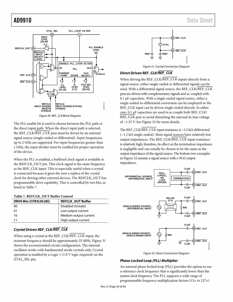
RAM MODULATION MODE The RAM modulation mode (see Figure 23) is activated via the RAM enable bit and assertion of the I/O_UPDATE pin (or a profile change). In this mode, the modulated DDS signal control parameters are supplied directly from RAM.
The RAM consists of 32-bit words and is 1024 words deep. Coupled with a sophisticated internal state machine, the RAM provides a very flexible method for generating arbitrary, time dependent waveforms. A programmable timer controls the rate at which words are extracted from the RAM for delivery to the DDS. Thus, the programmable timer establishes a sample rate at which 32-bit samples are supplied to the DDS.
The selection of the specific DDS signal control parameters that serve as the destination for the RAM samples is also programmable through eight independent RAM profile registers. Select a par-ticular profile using the three external profile pins (PROFILE[2:0]). A change in the state of the profile pins with the next rising edge on SYNC_CLK activates the selected RAM profile.
In RAM modulation mode, the ability to generate a time depen-dent amplitude, phase, or frequency signal enables modulation of any one of the parameters controlling the DDS carrier signal. Furthermore, a polar modulation format is available that partitions each RAM sample into a magnitude and phase component; 16 bits are allocated to phase and 14 bits are allocated to magnitude.
0647
9-00
6
16PARALLEL
INPUT
PDCLK
SCLK
SDIO
I/O_RESET
PROFILE[2:0]
I/O_UPDATE
RAM
EXT_
PWR
_DW
NDAC_RSET
IOUT
IOUT
CS
TxENABLE
DAC FSC
OSK A
θ INVERSESINC
FILTER
CLOCK
AMPLITUDE (A)
FREQUENCY (ω)
PHASE (θ)
DIGITALRAMP
GENERATOR
8
DAC FSC8
2
2
MULTICHIPSYNCHRONIZATION
SYSCLK
PLL
÷2
CLO
CK
MO
DE
REF_CLK
REF_CLK
REFCLK_OUT
XTAL_SELPARALLEL DATA
TIMING ANDCONTROL
SER
IAL
I/O P
OR
T2 AD9910
PROGRAMMINGREGISTERS
OUTPUTSHIFT
KEYING
DATAROUTE
ANDPARTITIONCONTROL
3
INTERNAL CLOCK TIMINGAND CONTROL
ω
Acos (ωt + θ)
Asin (ωt + θ)SY
NC
_SM
P_ER
R
SYN
C_O
UT
SYN
C_I
N
PLL_
LOC
K
PLL_
LOO
P_FI
LTER
MA
STER
_RES
ET2
2
DDS
AUXDAC8-BIT
DAC14-BIT
RAM_SWP_OVR
DRCTLDRHOLD
DROVER
SYN
C_C
LK
POWER-DOWN
CONTROL
Figure 23. RAM Modulation Mode

AD9910 Data Sheet
Rev. E | Page 18 of 64
DIGITAL RAMP MODULATION MODE In digital ramp modulation mode (see Figure 24), the modulated DDS signal control parameter is supplied directly from the digital ramp generator (DRG). The ramp generation parameters are controlled through the serial I/O port.
The ramp generation parameters allow the user to control both the rising and falling slopes of the ramp. The upper and lower boundaries of the ramp, the step size and step rate of the rising portion of the ramp, and the step size and step rate of the falling portion of the ramp are all programmable.
The ramp is digitally generated with 32-bit output resolution. The 32-bit output of the DRG can be programmed to represent frequency, phase, or amplitude. When programmed to represent frequency, all 32 bits are used. However, when programmed to represent phase or amplitude, only the 16 MSBs or 14 MSBs, respectively, are used.
The ramp direction (rising or falling) is externally controlled by the DRCTL pin. An additional pin (DRHOLD) allows the user to suspend the ramp generator in its present state.
0647
9-00
7
16PARALLEL
INPUT
PDCLK
SCLK
SDIO
I/O_RESET
PROFILE[2:0]
I/O_UPDATE
RAM
EXT_
PWR
_DW
N
DAC_RSET
IOUT
IOUT
CS
TxENABLE
DAC FSC
OSK A
θ INVERSESINC
FILTER
CLOCK
AMPLITUDE (A)
FREQUENCY (ω)
PHASE (θ)
DIGITALRAMP
GENERATOR
8
DAC FSC8
2
2
MULTICHIPSYNCHRONIZATION
SYSCLK
PLL
÷2
CLO
CK
MO
DE
REF_CLK
REF_CLK
REFCLK_OUT
XTAL_SELPARALLEL DATA
TIMING ANDCONTROL
SER
IAL
I/O P
OR
T2 AD9910
PROGRAMMINGREGISTERS
OUTPUTSHIFT
KEYING
DATAROUTE
ANDPARTITIONCONTROL
3
INTERNAL CLOCK TIMINGAND CONTROL
ω
Acos (ωt + θ)
Asin (ωt + θ)
SYN
C_S
MP_
ERR
SYN
C_O
UT
SYN
C_I
N
PLL_
LOC
K
PLL_
LOO
P_FI
LTER
MA
STER
_RES
ET2
2
DDS
AUXDAC8-BIT
DAC14-BIT
RAM_SWP_OVR
DRCTLDRHOLD
DROVERSY
NC
_CLK
POWER-DOWN
CONTROL
Figure 24. Digital Ramp Modulation Mode

Data Sheet AD9910
Rev. E | Page 19 of 64
PARALLEL DATA PORT MODULATION MODE In parallel data port modulation mode (see Figure 25), the modulated DDS signal control parameter(s) are supplied directly from the 18-bit parallel data port.
The data port is partitioned into two sections. The 16 MSBs make up a 16-bit data-word (D[15:0] pins) and the two LSBs make up a 2-bit destination word (F[1:0] pins). The destination word defines how the 16-bit data-word is applied to the DDS signal control parameters. Table 4 defines the relationship between the destination bits, the partitioning of the 16-bit data-word, and the destination of the data (in terms of the DDS signal control parameters). Formatting of the 16-bit data-word is unsigned binary, regardless of the destination.
When the destination bits indicate that the data-word is destined as a DDS frequency parameter, the 16-bit data-word serves as an offset to the 32-bit frequency tuning word in the FTW regis-ter. This means that the 16-bit data-word must somehow be properly aligned with the 32-bit word in the FTW register. This is accomplished by means of the 4-bit FM gain word in the programming registers. The FM gain word allows the user to
apply a weighting factor to the 16-bit data-word. In the default state (0), the 16-bit data-word and the 32-bit word in the FTW register are LSB aligned. Each increment in the value of the FM gain word shifts the 16-bit data-word to the left relative to the 32-bit word in the FTW register, increasing the influence of the 16-bit data-word on the frequency defined by the FTW register by a factor of two. The FM gain word effectively controls the frequency range spanned by the data-word.
Parallel Data Clock (PDCLK)
The AD9910 generates a clock signal on the PDCLK pin that runs at ¼ of the DAC sample rate (the sample rate of the par-allel data port). PDCLK serves as a data clock for the parallel port. By default, each rising edge of PDCLK is used to latch the 18 bits of user-supplied data into the data port. The edge polarity can be changed through the PDCLK invert bit. Furthermore, the PDCLK output signal can be switched off using the PDCLK enable bit. However, even though the output signal is switched off, it continues to operate internally using the internal PDCLK timing to capture the data at the parallel port. Note that PDCLK is Logic 0 when disabled.
0647
9-00
8
16
PARALLELINPUT
PDCLK
SCLK
SDIO
I/O_RESET
PROFILE[2:0]
I/O_UPDATE
RAM
POWER-DOWN
CONTROL
EX
T_P
WR
_DW
N
DAC_RSET
IOUT
IOUT
CS
TxENABLE
DAC FSC
OSK A
θ INVERSESINC
FILTER
CLOCK
AMPLITUDE (A)
FREQUENCY (ω)
PHASE (θ)
DIGITALRAMP
GENERATOR
8
DAC FSC8
2
2
MULTICHIPSYNCHRONIZATION
SYSCLK
PLL
÷2
CL
OC
K M
OD
E
REF_CLK
REF_CLK
REFCLK_OUT
XTAL_SEL
PARALLEL DATATIMING ANDCONTROL
SE
RIA
L I
/O P
OR
T2 AD9910
PROGRAMMINGREGISTERS
OUTPUTSHIFT
KEYING
DATAROUTE
ANDPARTITIONCONTROL
3
INTERNAL CLOCK TIMINGAND CONTROL
ω
Acos (ωt + θ)
Asin (ωt + θ)
SY
NC
_SM
P_E
RR
SY
NC
_OU
T
SY
NC
_IN
PL
L_L
OC
K
PL
L_L
OO
P_F
ILT
ER
MA
ST
ER
_RE
SE
T
22
DDS
AUXDAC8-BIT
DAC14-BIT
RAM_SWP_OVR
DRCTL
DRHOLD
DROVER
SY
NC
_CL
K
Figure 25. Parallel Data Port Modulation Mode

AD9910 Data Sheet
Rev. E | Page 20 of 64
Table 4. Parallel Port Destination Bits F[1:0] D[15:0] Parameter(s) Comments 00 D[15:2] 14-bit amplitude
parameter (unsigned integer)
Amplitude scales from 0 to 1 − 2−14. D[1:0] are not used.
01 D[15:0] 16-bit phase parameter (unsigned integer)
Phase offset ranges from 0 to 2(1 − 2−16) radians.
10 D[15:0] 32-bit frequency parameter (unsigned integer)
The alignment of the 16-bit data-word with the 32-bit frequency parameter is controlled by a 4-bit FM gain word in the programming registers.
11 D[15:8] 8-bit amplitude (unsigned integer)
The MSB of the data-word amplitude aligns with the MSB of the DDS 14-bit amplitude parameter. The six LSBs of the DDS amplitude parameter are assigned from Bits[5:0] of the ASF register. The resulting 14-bit word scales the amplitude from 0 to 1 − 2−14.
D[7:0] 8-bit phase (unsigned integer)
The MSB of the data-word phase aligns with the MSB of the 16-bit phase parameter of the DDS. The eight LSBs of the DDS phase parameter are assigned from Bits[7:0] of the POW register. The resulting 16-bit word offsets the phase from 0 to 2(1 − 2−16) radians.
Transmit Enable (TxENABLE)
The AD9910 also accepts a user-generated signal applied to the TxENABLE pin that acts as a gate for the user-supplied data. By default, TxENABLE is considered true for Logic 1 and false for Logic 0. However, the logical behavior of this pin can be reversed using the TxENABLE invert bit. When TxENABLE is true, the device latches data into the device on the expected edge of PDCLK (based on the PDCLK invert bit). When TxENABLE is false, even though the PDCLK may continue to operate, the device ignores the data supplied to the port. Furthermore, when the TxENABLE pin is held false, the device internally clears the 16-bit data-words, or it retains the last value present on the data port prior to TxENABLE switching to the false state (based on the setting of the data assembler hold last value bit).
Alternatively, instead of operating the TxENABLE pin as a gate, the user can drive the TxENABLE pin with a clock signal operating at the parallel port data rate. When driven by a clock signal, the transition from the false to true state must meet the required setup and hold time on each cycle to ensure proper operation. The TxENABLE and PDCLK timing is shown in Figure 26.
0647
9-00
9
FALSE
TRUETxENABLE
(BURST)
TxENABLE(CLOCK)
WORD1 WORD2 WORD3 WORD4 WORDN – 4 WORDN
PDCLK
PARALLELDATA PORT
tDS
tDStDH
tDH
Figure 26. PDCLK and TxENABLE Timing Diagram

Data Sheet AD9910
Rev. E | Page 21 of 64
MODE PRIORITY The three different modulation modes generate frequency, phase, and/or amplitude data destined for the DDS signal control parameters. In addition, the OSK function generates amplitude data destined for the DDS. Each of these functions is independently invoked using the appropriate control bit via the serial I/O port.
The ability to activate each of these functions independently makes it possible to have multiple data sources attempting to
drive the same DDS signal control parameter. To avoid contention, the AD9910 has a built-in priority system. Table 5 summarizes the priority for each of the DDS signal control parameters. The rows of Table 5 list data sources for a particular DDS signal con-trol parameter in descending order of precedence. For example, if both the RAM and the parallel port are enabled and both are programmed for frequency as the destination, then the DDS frequency parameter is driven by the RAM and not the parallel data port.
Table 5. Data Source Priority
Priority
DDS Signal Control Parameters Frequency Phase Amplitude
Data Source Conditions Data Source Conditions Data Source Conditions Highest Priority
RAM RAM enabled and data destination is frequency
RAM RAM enabled and data destination is phase or polar
OSK generator OSK enabled (auto mode)
DRG DRG enabled and data destination is frequency
DRG DRG enabled and data destination is phase
ASF register OSK enabled (manual mode)
Parallel data port and FTW register
Parallel data port enabled and data destination is frequency
Parallel data port Parallel data port enabled and data destination is phase
RAM RAM enabled and data destination is amplitude or polar
FTW register RAM enabled and data destination is phase, amplitude, or polar
Parallel data port concatenated with the POW register LSBs
Parallel data port enabled and data destination is polar
DRG DRG enabled and data destination is amplitude
FTW in active single tone profile register
DRG enabled and data destination is phase or amplitude
POW register RAM enabled and destination is frequency or amplitude
Parallel data port Parallel data port enabled and data destination is amplitude
FTW in active single tone profile register
Parallel data port enabled and data destination is phase, amplitude, or polar
POW in active single tone profile register
DRG enabled and data destination is frequency or amplitude
Parallel data port concatenated with the ASF register LSBs
Parallel data port enabled and data destination is polar
FTW in active single tone profile register
None POW in active single tone profile register
Parallel data port enabled and data destination is frequency or amplitude
ASF in active single tone profile register
Enable amplitude scale from single tone profiles bit (CFR2[24]) set
Lowest Priority
POW in active single tone profile register
None No amplitude scaling
None

AD9910 Data Sheet
Rev. E | Page 22 of 64
FUNCTIONAL BLOCK DETAIL DDS CORE The direct digital synthesizer (DDS) block generates a reference signal (sine or cosine based on CFR1[16], the select DDS sine output bit). The parameters of the reference signal (frequency, phase, and amplitude) are applied to the DDS at its frequency, phase offset, and amplitude control inputs, as shown in Figure 27.
0647
9-01
0
DDS_CLK
32 19FREQUENCYCONTROL
ANGLE-TO-AMPLITUDE
CONVERSION(SINE ORCOSINE)
PHASEOFFSET
CONTROL
TO DAC(MSBs)
D Q
R
ACCUMULATORRESET
32
16
MSB ALIGNED
AMPLITUDECONTROL
14
DDS SIGNAL CONTROL PARAMETERS
16
1419
32
32 14
1432-BIT
ACCUMULATOR
Figure 27. DDS Block Diagram
The output frequency (fOUT) of the AD9910 is controlled by the frequency tuning word (FTW) at the frequency control input to the DDS. The relationship among fOUT, FTW, and fSYSCLK is given by
SYSCLKOUT fFTWf
= 322
(1)
where FTW is a 32-bit integer ranging in value from 0 to 2,147,483,647 (231 − 1), which represents the lower half of the full 32-bit range. This range constitutes frequencies from dc to Nyquist (that is, ½ fSYSCLK).
The FTW required to generate a desired value of fOUT is found by solving Equation 1 for FTW, as given in Equation 2.
=
SYSCLK
OUT
ff
FTW 322round (2)
where the round(x) function rounds the argument (the value of x) to the nearest integer. This is required because the FTW is constrained to be an integer value. For example, for fOUT = 41 MHz and fSYSCLK = 122.88 MHz, then FTW = 1,433,053,867 (0x556AAAAB).
Programming an FTW greater than 231 produces an aliased image that appears at a frequency given by
SYSCLKOUT fFTWf
−= 3221 (for FTW ≥ 231)
The relative phase of the DDS signal can be digitally controlled by means of a 16-bit phase offset word (POW). The phase offset is applied prior to the angle-to-amplitude conversion block internal to the DDS core. The relative phase offset (Δθ) is given by
=
16
16
2360
22
ΔPOW
POWπθ
where the upper quantity is for the phase offset expressed as radian units and the lower quantity as degrees. To find the POW value necessary to develop an arbitrary Δθ, solve the previous equation for POW and round the result (in a manner similar to that described previously for finding an arbitrary FTW).
The relative amplitude of the DDS signal can be digitally scaled (relative to full scale) by means of a 14-bit amplitude scale factor (ASF). The amplitude scale value is applied at the output of the angle-to-amplitude conversion block internal to the DDS core. The amplitude scale is given by
=
14
14
2log20
2ASF
ASF
ScaleAmplitude (3)
where the upper quantity is amplitude expressed as a fraction of full scale and the lower quantity is expressed in decibels relative to full scale. To find the ASF value necessary for a particular scale factor, solve Equation 3 for ASF and round the result (in a manner similar to that described previously for finding an arbitrary FTW).
When the AD9910 is programmed to modulate any of the DDS signal control parameters, the maximum modulation sample rate is ¼ fSYSCLK. This means that the modulation signal exhibits images at multiples of ¼ fSYSCLK. The impact of these images must be considered when using the device as a modulator.
14-BIT DAC OUTPUT The AD9910 incorporates an integrated 14-bit, current output DAC. The output current is delivered as a balanced signal using two outputs. The use of balanced outputs reduces the potential amount of common-mode noise present at the DAC output, offering the advantage of an increased signal-to-noise ratio. An external resistor (RSET) connected between the DAC_RSET pin and AGND establishes the reference current. The full-scale output current of the DAC (IOUT) is produced as a scaled version of the reference current (see the Auxiliary DAC section). The recommended value of RSET is 10 kΩ.
Attention should be paid to the load termination to keep the output voltage within the specified compliance range; voltages developed beyond this range cause excessive distortion and can damage the DAC output circuitry.
Data Sheet AD9910
Rev. E | Page 23 of 64
Auxiliary DAC
An 8-bit auxiliary DAC controls the full-scale output current of the main DAC (IOUT). An 8-bit code word stored in the appropriate register map location sets IOUT according to the following equation:
+=
9614.86 CODE
RI
SETOUT
where RSET is the value of the RSET resistor (in ohms) and CODE is the 8-bit value supplied to the auxiliary DAC (default is 127). For example, with RSET = 10,000 Ω and CODE = 127, then IOUT = 20.07 mA.
INVERSE SINC FILTER The sampled carrier data stream is the input to the digital-to-analog converter (DAC) integrated into the AD9910. The DAC output spectrum is shaped by the characteristic sin(x)/x (or sinc) envelope, due to the intrinsic zero-order hold effect associated with DAC generated signals. The sinc envelope can be compensated for because its shape is well known. This envelope restoration function is provided by the inverse sinc filter preceding the DAC. The inverse sinc filter is implemented as a digital FIR filter. It has a response characteristic that very nearly matches the inverse of the sinc envelope. The response of the inverse sinc filter is shown in Figure 28 (with the sinc envelope for comparison).
The inverse sinc filter is enabled using CFR1[22]. The filter tap coefficients are given in Table 6. The filter operates by distorting the data prior to its arrival at the DAC in such a way as to compensate for the sinc envelope that otherwise distorts the spectrum.
When the inverse sinc filter is enabled, it introduces a ~3.0 dB insertion loss. The inverse sinc compensation is effective for output frequencies up to approximately 40% of the DAC sample rate.
Table 6. Inverse Sinc Filter Tap Coefficients Tap No. Tap Value 1, 7 −35 2, 6 +134 3, 5 −562 4 +6729
In Figure 28, the sinc envelope introduces a frequency dependent attenuation that can be as much as 4 dB at the Nyquist frequency (½ of the DAC sample rate). Without the inverse sinc filter, the DAC output suffers from the frequency dependent droop of the sinc envelope. The inverse sinc filter effectively flattens the droop to within ±0.05 dB, as shown in Figure 29, which shows the corrected sinc response with the inverse sinc filter enabled.
1
0
–1
–2
–3
–40 0.1 0.2 0.40.3 0.5
0647
9-01
1
(dB
)
FREQUENCY RELATIVE TO DAC SAMPLE RATE
INVERSESINC
SINC
Figure 28. Sinc and Inverse Sinc Responses
–2.8
–2.9
–3.0
–3.10 0.1 0.2 0.40.3 0.5
0647
9-01
2
(dB
)
FREQUENCY RELATIVE TO DAC SAMPLE RATE
COMPENSATED RESPONSE
Figure 29. DAC Response with Inverse Sinc Compensation
CLOCK INPUT (REF_CLK/REF_CLK)
REF_CLK/REF_CLK Overview
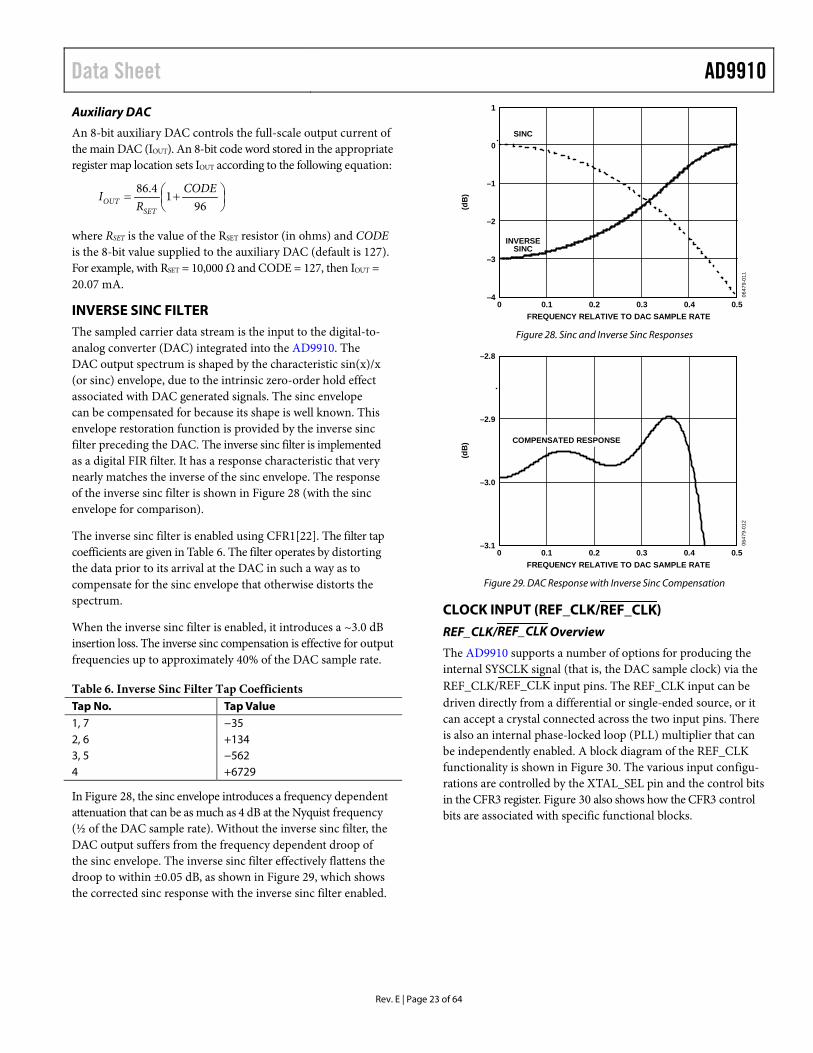
The AD9910 supports a number of options for producing the internal SYSCLK signal (that is, the DAC sample clock) via the REF_CLK/REF_CLK input pins. The REF_CLK input can be driven directly from a differential or single-ended source, or it can accept a crystal connected across the two input pins. There is also an internal phase-locked loop (PLL) multiplier that can be independently enabled. A block diagram of the REF_CLK functionality is shown in Figure 30. The various input configu-rations are controlled by the XTAL_SEL pin and the control bits in the CFR3 register. Figure 30 also shows how the CFR3 control bits are associated with specific functional blocks.
AD9910 Data Sheet
Rev. E | Page 24 of 64
REF_CLK
REF_CLK
PLL
VCOSELECTDIVIDE
CHARGEPUMP
OUTIN
PLL_LOOP_FILTERENABLE
PLL_LOOP_FILTER
DRV0CFR3
[29:28]
REFCLK_OUT
XTAL_SEL
REFCLKINPUT
SELECTLOGIC
SYSCLK
ICPCFR3
[21:19]
NCFR3[7:1]
VCO SELCFR3
[26:24]
÷2
REFCLKINPUT DIVIDER BYPASSCFR3[15]
PLL ENABLECFR3
[8]
REFCLKINPUT DIVIDER
RESETBCFR3[14]
94
95 2
90
91
01
01
2
2
7 3
01
0647
9-01
3
Figure 30. REF_CLK Block Diagram
The PLL enable bit is used to choose between the PLL path or the direct input path. When the direct input path is selected, the REF_CLK/REF_CLK pins must be driven by an external signal source (single-ended or differential). Input frequencies up to 2 GHz are supported. For input frequencies greater than 1 GHz, the input divider must be enabled for proper operation of the device.
When the PLL is enabled, a buffered clock signal is available at the REFCLK_OUT pin. This clock signal is the same frequency as the REF_CLK input. This is especially useful when a crystal is connected because it gives the user a replica of the crystal clock for driving other external devices. The REFCLK_OUT has programmable drive capability. This is controlled by two bits, as listed in Table 7.
Table 7. REFCLK_OUT Buffer Control DRV0 Bits (CFR3[29:28]) REFCLK_OUT Buffer 00 Disabled (tristate) 01 Low output current 10 Medium output current 11 High output current
Crystal Driven REF_CLK/REF_CLK
When using a crystal at the REF_CLK/REF_CLK input, the resonant frequency should be approximately 25 MHz. Figure 31 shows the recommended circuit configuration. The internal oscillator works with fundamental mode crystals only. Crystal operation is enabled by a Logic 1 (1.8 V logic required) on the XTAL_SEL pin.
0647
9-01
4
REF_CLK
REF_CLK39pF39pF
XTAL
90
91
Figure 31. Crystal Connection Diagram
Direct Driven REF_CLK/REF_CLK
When driving the REF_CLK/REF_CLK inputs directly from a signal source, either single-ended or differential signals can be used. With a differential signal source, the REF_CLK/REF_CLK pins are driven with complementary signals and ac-coupled with 0.1 µF capacitors. With a single-ended signal source, either a single-ended-to-differential conversion can be employed or the REF_CLK input can be driven single-ended directly. In either case, 0.1 µF capacitors are used to ac couple both REF_CLK/ REF_CLK pins to avoid disturbing the internal dc bias voltage of ~1.35 V. See Figure 32 for more details.
The REF_CLK/REF_CLK input resistance is ~2.5 kΩ differential (~1.2 kΩ single-ended). Most signal sources have relatively low output impedances. The REF_CLK/REF_CLK input resistance is relatively high; therefore, its effect on the termination impedance is negligible and can usually be chosen to be the same as the output impedance of the signal source. The bottom two examples in Figure 32 assume a signal source with a 50 Ω output impedance.
0647
9-01
5
TERMINATION
REF_CLK
DIFFERENTIAL SOURCE,DIFFERENTIAL INPUT
SINGLE-ENDED SOURCE,DIFFERENTIAL INPUT
SINGLE-ENDED SOURCE,SINGLE-ENDED INPUT
90
91
0.1µF
0.1µF
PECL,LVPECL,
ORLVDS
DRIVER
REF_CLK90
91
50Ω
0.1µF
0.1µF
BALUN(1:1)
REF_CLK
REF_CLK
REF_CLK
REF_CLK
90
910.1µF
0.1µF
50Ω
Figure 32. Direct Connection Diagram
Phase-Locked Loop (PLL) Multiplier
An internal phase-locked loop (PLL) provides the option to use a reference clock frequency that is significantly lower than the system clock frequency. The PLL supports a wide range of programmable frequency multiplication factors (12× to 127×)

Data Sheet AD9910
Rev. E | Page 25 of 64
as well as a programmable charge pump current and external loop filter components (connected via the PLL_LOOP_FILTER pin). These features add an extra layer of flexibility to the PLL, allowing optimization of phase noise performance and flexibility in frequency plan development. The PLL is also equipped with a PLL_LOCK pin.
The PLL output frequency range (fSYSCLK) is constrained to the range of 420 MHz ≤ fSYSCLK ≤ 1 GHz by the internal VCO. In addition, the user must program the VCO to one of six operating ranges such that fSYSCLK falls within the specified range. Figure 33 and Figure 34 summarize these VCO ranges.
Figure 33 shows the boundaries of the VCO frequency ranges over the full range of temperature and supply voltage variation for all devices from the available population. The implication is that multiple devices chosen at random from the population and operated under widely varying conditions may require different values to be programmed into CFR3[26:24] to operate at the same frequency. For example, Part A chosen randomly from the population, operating at an ambient temperature of −10°C with a system clock frequency of 900 MHz may require CFR3[26:24] to be set to 100b, whereas Part B chosen randomly from the population, operating at an ambient temperature of 90°C with a system clock frequency of 900 MHz may require CFR3[26:24] to be set to 101b. If a frequency plan is chosen such that the system clock frequency operates within one set of boundaries (as shown in Figure 33), the required value in CFR3[26:24] is consistent from part to part.
Figure 34 shows the boundaries of the VCO frequency ranges over the full range of temperature and supply voltage variation for an individual device selected from the population. Figure 34 shows that the VCO frequency ranges for a single device always overlap when operated over the full range of conditions.
If a user wants to retain a single default value for CFR3[26:24], a frequency that falls into one of the ranges found in Figure 33 should be selected. Additionally, for any given individual device, the VCO frequency ranges overlap, meaning that any given device exhibits no gaps in its frequency coverage across VCO ranges over the full range of conditions.
0647
9-05
9
VCO0
VCO1
VCO2
VCO3
VCO4
VCO5
395 495 595 695 795 895 995
fLOW = 400fHIGH = 460
fLOW = 455fHIGH = 530
fLOW = 530fHIGH = 615
fLOW = 760fHIGH = 875
fLOW = 920fHIGH = 1030
fLOW = 650fHIGH = 790
(MHz) Figure 33. VCO Ranges Including Atypical Wafer Process Skew
335 435 535 635 735 835 935 1035 1135
VCO0
VCO1
VCO2
VCO3
VCO4
VCO5
0647
9-06
0fLOW = 370fHIGH = 510
fLOW = 420fHIGH = 590
fLOW = 500fHIGH = 700
fLOW = 700fHIGH = 950
fLOW = 820fHIGH = 1150
fLOW = 600fHIGH = 880
(MHz) Figure 34. Typical VCO Ranges
Table 8. VCO Range Bit Settings VCO SEL Bits (CFR3[26:24]) VCO Range
000 VCO0 001 VCO1 010 VCO2 011 VCO3 100 VCO4 101 VCO5 110 PLL bypassed 111 PLL bypassed
PLL Charge Pump
The charge pump current (ICP) is programmable to provide the user with additional flexibility to optimize the PLL performance. Table 9 lists the bit settings vs. the nominal charge pump current.
Table 9. PLL Charge Pump Current ICP Bits (CFR3[21:19]) Charge Pump Current, ICP (μA)
000 212 001 237 010 262 011 287 100 312 101 337 110 363 111 387

AD9910 Data Sheet
Rev. E | Page 26 of 64
External PLL Loop Filter Components
The PLL_LOOP_FILTER pin provides a connection interface to attach the external loop filter components. The ability to use custom loop filter components gives the user more flexibility to optimize the PLL performance. The PLL and external loop filter components are shown in Figure 35.
PFD CP
PLL_LOOP_FILTER
VCO
÷N
PLL OUTPLL IN
AVDD
REFCLK PLL
2
R1
C1
C2
0647
9-01
6
Figure 35. REFCLK PLL External Loop Filter
In the prevailing literature, this configuration yields a third-order, Type II PLL. To calculate the loop filter component values, begin with the feedback divider value (N), the gain of the phase detector (KD), and the gain of the VCO (KV) based on the programmed VCO SEL bit settings (see Table 1 for KV). The loop filter component values depend on the desired open-loop bandwidth (fOL) and phase margin (φ), as follows:
( )
+=
φKKNfπ
R1VD
OL
sin11 (4)
( )( ) 22
tan
OL
VD
fπNφKK
C1 = (5)
( )( )( )
−=
φφ
fπNKK
C2OL
VD
cossin1
2 2 (6)
where: KD is equal to the programmed value of ICP. KV is taken from Table 1.
Ensure that proper units are used for the variables in Equation 4 through Equation 6. ICP must be in amps, not microamps (μA) as appears in Table 9; KV must be in hertz per volts (Hz/V), not megahertz per volts (MHz/V) as listed in Table 1; the loop bandwidth (fOL) must be in hertz (Hz); the phase margin (φ) must be in radians.
For example, suppose the PLL is programmed such that ICP = 287 μA, KV = 625 MHz/V, and N = 25. If the desired loop bandwidth and phase margin are 50 kHz and 45°, respectively, then the loop filter component values are R1 = 52.85 Ω, C1 = 145.4 nF, and C2 = 30.11 nF.
PLL LOCK INDICATION When the PLL is in use, the PLL_LOCK pin provides an active high indication that the PLL has locked to the REFCLK input signal. Note that the PLL_LOCK pin is a latched output. When the PLL is bypassed, the pin may remain at Logic 1. The PLL_LOCK pin can be cleared by setting the PFD reset bit. The PFD reset bit must be cleared for normal operation.
OUTPUT SHIFT KEYING (OSK) The OSK function (see Figure 36) allows the user to control the output signal amplitude of the DDS. Both a manual and an automatic mode are available under program control. The amplitude data generated by the OSK block has priority over any other functional block that is programmed to deliver amplitude data to the DDS. Therefore, the OSK data source, when enabled, overrides all other amplitude data sources.
0647
9-01
7
OSK ENABLE
AMPLITUDE SCALE FACTOR(ASF[15:2])
AMPLITUDE RAMP RATE(ASF[31:16])
AMPLITUDE STEP SIZE(ASF[1:0])
MANUAL OSK EXTERNAL
AUTO OSK ENABLE
OSK
DDS CLOCK
TO DDSAMPLITUDECONTROLPARAMETER
60
LOAD ARR AT I/O_UPDATE
OSKCONTROLLER
1416
14
2
Figure 36. OSK Block Diagram
The operation of the OSK function is governed by two CFR1 register bits (OSK enable and select auto OSK), the external OSK pin, and the entire 32 bits of the ASF register. The primary control for the OSK block is the OSK Enable bit. When the OSK function is disabled, the OSK input controls are ignored and the internal clocks shut down.
When the OSK function is enabled, automatic or manual operation is selected using the select auto OSK bit. A Logic 0 indicates manual mode (default).
Manual OSK
In manual mode, output amplitude is varied by successive write operations to the amplitude scale factor portion of the ASF register. The rate at which amplitude changes can be applied to the output signal is limited by the speed of the serial I/O port. In manual mode, the OSK pin functionality depends on the state of the manual OSK external control bit. When the OSK pin is Logic 0, the output amplitude is forced to 0; otherwise, the output amplitude is set by the amplitude scale factor value.

Data Sheet AD9910
Rev. E | Page 27 of 64
Automatic OSK
In automatic mode, the OSK function automatically generates a linear amplitude vs. time profile (or amplitude ramp). The ampli-tude ramp is controlled via three parameters: the maximum amplitude scale factor, the amplitude step size, and the time interval between steps. The amplitude ramp parameters reside in the 32-bit ASF register and are programmed via the serial I/O port. The time interval between amplitude steps is set via the 16-bit amplitude ramp rate portion of the ASF register (Bits[31:16]). The maximum amplitude scale factor is set via the 14-bit amplitude scale factor in the ASF register (Bits[15:2]). The amplitude step size is set via the 2-bit amplitude step size portion of the ASF register (Bits[1:0]). Additionally, the direction of the ramp (positive or negative slope) is controlled by the external OSK pin.
The step interval is controlled by a 16-bit programmable timer that is clocked at a rate of ¼ fSYSCLK. The period of the timer sets the time interval between amplitude steps. The step time interval (Δt) is given by
SYSCLKfMt 4Δ
where M is the 16-bit number stored in the amplitude ramp rate (ARR) portion of the ASF register. For example, if fSYSCLK = 750 MHz and M = 23218 (0x5AB2), then Δt ≈ 123.8293 μs.
The output of the OSK function is a 14-bit unsigned data bus that controls the amplitude parameter of the DDS (as long as the OSK enable bit is set). When the OSK pin is set, the OSK output value starts at 0 (zero) and increments by the pro-grammed amplitude step size until it reaches the programmed maximum amplitude value. When the OSK pin is cleared, the OSK output starts at its present value and decrements by the programmed amplitude step size until it reaches 0 (zero).
The OSK output does not necessarily attain the maximum amplitude value if the OSK pin is switched to Logic 0 before the maximum value is reached. Nor does the OSK output necessarily reach a value of 0 if the OSK pin is switched to Logic 1 before the 0 value is reached.
The OSK output is initialized to 0 (zero) at power-up and reset whenever the OSK enable bit or the select auto OSK bit is cleared.
The amplitude step size of the OSK output is set by the amplitude step size bits in the ASF register according to Table 10. The step size refers to the LSB weight of the 14-bit OSK output. Regardless of the programmed step size, the OSK output does not exceed the maximum amplitude value programmed into the ASF register.
Table 10. OSK Amplitude Step Size Amplitude Step Size Bits (ASF[1:0]) Amplitude Step Size 00 1 01 2 10 4 11 8
As mentioned previously, a 16-bit programmable timer controls the step interval. Normally, this timer is loaded with the pro-grammed timing value whenever the timer expires, initiating a new timing cycle. However, there are three events that can cause reloading of the timer to have its timing value reloaded prior to the timer expiring. One such event occurs when the select auto OSK bit transitions from cleared to set, followed by an I/O update. A second such event is a change of state in the OSK pin. The third is dependent on the status of the load ARR @ I/O update bit. If this bit is cleared, then no action occurs; otherwise, when the I/O_UPDATE pin is asserted (or a profile change occurs), the timer is reset to its initial starting point.
DIGITAL RAMP GENERATOR (DRG) DRG Overview
To sweep phase, frequency, or amplitude from a defined start point to a defined endpoint, a completely digital, digital ramp generator is included in the AD9910. The DRG makes use of nine control register bits, three external pins, two 64-bit registers, and one 32-bit register (see Figure 37).
DIGITAL RAMP LIMIT REGISTER
DR
CTL
DDS CLOCK
DR
HO
LD
DR
OVE
R
DIGITAL RAMP RATE REGISTER
DIGITAL RAMP STEP REGISTER
0647
9-01
8
TO DDSSIGNALCONTROLPARAMETER
DIGITAL RAMP ENABLE
DROVER PIN ACTIVELOAD LRR AT I/O_UPDATE
CLEAR DIGITALRAMP ACCUMULATOR
AUTOCLEAR DIGITALRAMP ACCUMULATOR
64
64
DIGITAL RAMP DESTINATION2
DIGITAL RAMP NO-DWELL2
32
32DIGITALRAMP
GENERATOR
62 61 63
Figure 37. Digital Ramp Block Diagram

AD9910 Data Sheet
Rev. E | Page 28 of 64
The primary control for the DRG is the digital ramp enable bit. When disabled, the other DRG input controls are ignored and the internal clocks are shut down to conserve power.
The output of the DRG is a 32-bit unsigned data bus that can be routed to any one of the three DDS signal control parameters, as controlled by the two digital ramp destination bits in Control Function Register 2 according to Table 11. The 32-bit output bus is MSB-aligned with the 32-bit frequency parameter, the 16-bit phase parameter, or the 14-bit amplitude parameter, as defined by the destination bits. When the destination is phase or amplitude, the unused LSBs are ignored.
Table 11. Digital Ramp Destination Digital Ramp Destination Bits (CFR2[21:20])
DDS Signal Control Parameter
Bits Assigned to DDS Parameter
00 Frequency 31:0 01 Phase 31:16 1x1 Amplitude 31:18 1 x = Don’t care.
The ramp characteristics of the DRG are fully programmable. This includes the upper and lower ramp limits, and independent control of the step size and step rate for both the positive and negative slope characteristics of the ramp. A detailed block diagram of the DRG is shown in Figure 38.
The direction of the ramping function is controlled by the DRCTL pin. A Logic 0 on this pin causes the DRG to ramp with a negative slope, whereas a Logic 1 causes the DRG to ramp with a positive slope.
The DRG also supports a hold feature controlled via the DRHOLD pin. When this pin is set to Logic 1, the DRG is stalled at its last state; otherwise, the DRG operates normally.
The DDS signal control parameters that are not the destination of the DRG are taken from the active profile.
DDS CLOCK
D Q
R
LOWERLIMIT
0
1
DECREMENT STEP SIZE
PRESET
Q
DRCTL
LOAD
CLEAR DIGITAL RAMP ACCUMULATOR
AUTOCLEAR DIGITAL RAMP ACC.
NO DWELL
LIMIT CONTROL
DIGITAL RAMP ACCUMULATOR
INCREMENT STEP SIZE
32
32
0
1
NEGATIVE SLOPE RATE
POSITIVE SLOPE RATE
16
16
32
16
62
DRHOLD 63
32
32
LOADCONTROL
LOGICLOAD LRR AT I/O_UPDATE
DIGITALRAMPTIMER
ACCUMULATORRESET
CONTROLLOGIC
NO-DWELLCONTROL
2
3232
TO DDSSIGNALCONTROLPARAMETER
UPPERLIMIT
32
0647
9-01
9
Figure 38. Digital Ramp Generator Detail

Data Sheet AD9910
Rev. E | Page 29 of 64
DRG Slope Control
The core of the DRG is a 32-bit accumulator clocked by a programmable timer. The time base for the timer is the DDS clock, which operates at ¼ fSYSCLK. The timer establishes the interval between successive updates of the accumulator. The positive (+Δt) and negative (−Δt) slope step intervals are independently programmable as given by
SYSCLKfPt 4Δ =+
SYSCLKfNt 4Δ =−
where P and N are the two 16-bit values stored in the 32-bit digital ramp rate register and control the step interval. N defines the step interval of the negative slope portion of the ramp. P defines the step interval of the positive slope portion of the ramp.
The step size of the positive (STEPP) and negative (STEPN) slope portions of the ramp are 32-bit values programmed into the 64-bit digital ramp step size register. Program each of the step sizes as an unsigned integer (the hardware automatically interprets STEPN as a negative value). The relationship between the 32-bit step size values and actual units of frequency, phase, or amplitude depend on the digital ramp destination bits. Calculate the actual frequency, phase, or amplitude step size by substituting STEPN or STEPP for M in the following equations as required:
SYSCLKfMStepFrequency
= 322
312MStepPhase π
= (radians)
29245MStepPhase = (degrees)
FSIMStepAmplitude
= 322
Note that the frequency units are the same as those used to represent fSYSCLK (MHz, for example). The amplitude units are the same as those used to represent IFS, the full-scale output current of the DAC (mA, for example).
The phase and amplitude step size equations yield the average step size. Although the step size accumulates with 32-bit precision, the phase or amplitude destination exhibits only 16 or 14 bits, respectively. Therefore, at the destination, the actual phase or amplitude step is the accumulated 32-bit value truncated to 16 or 14 bits, respectively.
As described previously, the step interval is controlled by a 16-bit programmable timer. There are three events that can cause this timer to be reloaded prior to its expiration.
One event occurs when the digital ramp enable bit transitions from cleared to set, followed by an I/O update. A second event is a change of state in the DRCTL pin. The third event is enabled using the load LRR @ I/O update bit (see the Register Map and Bit Descriptions section for details).
DRG Limit Control
The ramp accumulator is followed by limit control logic that enforces an upper and lower boundary on the output of the ramp generator. Under no circumstances does the output of the DRG exceed the programmed limit values while the DRG is enabled. The limits are set through the 64-bit digital ramp limit register. Note that the upper limit value must be greater than the lower limit value to ensure normal operation.
DRG Accumulator Clear
The ramp accumulator can be cleared (that is, reset to 0) under program control. When the ramp accumulator is cleared, it forces the DRG output to the lower limit programmed into the digital ramp limit register.
With the limit control block embedded in the feedback path of the accumulator, resetting the accumulator is equivalent to presetting it to the lower limit value.
Normal Ramp Generation
Normal ramp generation implies that both no-dwell bits are cleared (see the No-Dwell Ramp Generation section for details). In Figure 39, a sample ramp waveform is depicted with the required control signals. The top trace is the DRG output. The next trace down is the status of the DROVER output pin (assuming that the DROVER pin active bit is set). The remaining traces are control bits and control pins. The pertinent ramp parameters are also identified (upper and lower limits plus step size and Δt for the positive and negative slopes). Along the bottom, circled numbers identify specific events. These events are referred to by number (Event 1 and so on) in the following paragraphs.
In this particular example, the positive and negative slopes of the ramp are different to demonstrate the flexibility of the DRG. The parameters of both slopes can be programmed to make the positive and negative slopes the same.

AD9910 Data Sheet
Rev. E | Page 30 of 64
DRG OUTPUT
LOWER LIMIT
UPPER LIMIT
DRCTL
DRHOLD
AUTOCLEAR DIGITALRAMP ACCUMULATOR
CLEAR DIGITALRAMP ACCUMULATOR
I/O_UPDATE
POSITIVESTEP SIZE
NEGATIVESTEP SIZE
P DDS CLOCK CYCLES N DDS CLOCK CYCLES 1 DDS CLOCK CYCLE
DIGITAL RAMP ENABLE
DROVER
0647
9-02
0
CL
EA
R
RE
LE
AS
E
AU
TO
CL
EA
R
–∆t+∆t
1 2 3 4 5 6 7 8 9
10
11
12
13
Figure 39. Normal Ramp Generation
Event 1—The digital ramp enable bit is set, which has no effect on the DRG output because the bit is not effective until an I/O update.
Event 2—An I/O update registers the enable bit. If DRCTL = 1 is in effect at this time (the gray portion of the DRCTL trace), then the DRG output immediately begins a positive slope (the gray portion of the DRG output trace). Otherwise, if DRCTL = 0, the DRG output is initialized to the lower limit.
Event 3—DRCTL transitions to a Logic 1 to initiate a positive slope at the DRG output. In this example, the DRCTL pin is held long enough to cause the DRG to reach its programmed upper limit. The DRG remains at the upper limit until the ramp accumulator is cleared, DRCTL = 0, or the upper limit is reprogrammed to a higher value. In the last case, the DRG immediately resumes its previous positive slope profile.
Event 4—DRCTL transitions to a Logic 0 to initiate a negative slope at the DRG output. In this example, the DRCTL pin is held long enough to cause the DRG to reach its programmed lower limit. The DRG remains at the lower limit until DRCTL = 1, or until the lower limit is reprogrammed to a lower value. In the latter case, the DRG immediately resumes its previous negative slope profile.
Event 5—DRCTL transitions to a Logic 1 for the second time, initiating a second positive slope.
Event 6—The positive slope profile is interrupted by DRHOLD transitioning to a Logic 1. This stalls the ramp accumulator and freezes the DRG output at its last value.
Event 7—DRHOLD transitions to a Logic 0, releasing the ramp accumulator and reinstating the previous positive slope profile.
Event 8—The clear digital ramp accumulator bit is set, which has no effect on the DRG because the bit is not effective until an I/O update is issued.
Event 9—An I/O update registers that the clear digital ramp accumulator bit is set, resetting the ramp accumulator and forcing the DRG output to the programmed lower limit. The DRG output remains at the lower limit until the clear condition is removed.
Event 10—The clear digital ramp accumulator bit is cleared, which has no effect on the DRG output because the bit is not effective until an I/O update is issued.
Event 11—An I/O update registers that the clear digital ramp accumulator bit is cleared, releasing the ramp accumulator, and the previous positive slope profile restarts.
Event 12—The autoclear digital ramp accumulator bit is set, which has no effect on the DRG output because the bit is not effective until an I/O update is issued.
Event 13—An I/O update registers that the autoclear digital ramp accumulator bit is set, resetting the ramp accumulator. However, with an automatic clear, the ramp accumulator is only held reset for a single DDS clock cycle. This forces the DRG output to the lower limit, but the ramp accumulator is immedi-ately made available for normal operation. In this example, the DRCTL pin remains a Logic 1; therefore, the DRG output restarts the previous positive ramp profile.

Data Sheet AD9910
Rev. E | Page 31 of 64
No-Dwell Ramp Generation
The two no-dwell bits in Control Function Register 2 add to the flexibility of the DRG capabilities. During normal ramp generation, when the DRG output reaches the programmed upper or lower limit, it simply remains at the limit until the operating parameters dictate otherwise. However, during no-dwell operation, the DRG output does not necessarily remain at the limit. For example, if the digital ramp no-dwell high bit is set when the DRG reaches the upper limit, it automatically (and immediately) snaps to the lower limit (that is, it does not ramp back to the lower limit; it jumps to the lower limit). Likewise, when the digital ramp no-dwell low bit is set, and the DRG reaches the lower limit, it automatically (and immediately) snaps to the upper limit.
During no-dwell operation, the DRCTL pin is monitored for state transitions only; that is, the static logic level is immaterial.
During no-dwell high operation, a positive transition of the DRCTL pin initiates a positive slope ramp, which continues uninterrupted (regardless of any further activity on the DRCTL pin) until the upper limit is reached.
During no-dwell low operation, a negative transition of the DRCTL pin initiates a negative slope ramp, which continues uninterrupted (regardless of any further activity on the DRCTL pin) until the lower limit is reached.
Setting both no-dwell bits invokes a continuous ramping mode of operation; that is, the DRG output automatically oscillates between the two limits using the programmed slope parameters. Furthermore, the function of the DRCTL pin is slightly different. Instead of controlling the initiation of the ramp sequence, it only serves to change the direction of the ramp; that is, if the DRG output is in the midst of a positive slope and the DRCTL pin transitions from Logic 1 to Logic 0, then the DRG imme-diately switches to the negative slope parameters and resumes oscillation between the limits. Likewise, if the DRG output is in the midst of a negative slope and the DRCTL pin transitions from Logic 0 to Logic 1, the DRG immediately switches to the positive slope parameters and resumes oscillation between the limits.
When both no-dwell bits are set, the DROVER signal produces a positive pulse (two cycles of the DDS clock) each time the DRG output reaches either of the programmed limits (assuming that the DROVER pin active bit is set).
A no-dwell high DRG output waveform is shown in Figure 40. The waveform diagram assumes that the digital ramp no-dwell high bit is set and has been registered by an I/O update. The status of the DROVER pin is also shown with the assumption that the DROVER pin active bit has been set.
UPPER LIMIT
P DDS CLOCK CYCLES
1 2 3 4 5 6 7 8
DRG OUTPUT
LOWER LIMIT
DRCTL
POSITIVESTEP SIZE
DROVER
+Δt
0647
9-02
1
Figure 40. No-Dwell High Ramp Generation
The circled numbers in Figure 40 indicate specific events, which are explained as follows:
Event 1—Indicates the instant that an I/O update registers that the digital ramp enable bit has been set.
Event 2—DRCTL transitions to a Logic 1, initiating a positive slope at the DRG output.
Event 3—DRCTL transition to a Logic 0, which has no effect on the DRG output.
Event 4—Because the digital ramp no-dwell high bit is set, the moment that the DRG output reaches the upper limit, it immediately switches to the lower limit, where it remains until the next Logic 0 to Logic 1 transition of DRCTL.
Event 5—DRCTL transitions from Logic 0 to Logic 1, which restarts a positive slope ramp.
Event 6 and Event 7—DRCTL transitions are ignored until the DRG output reaches the programmed upper limit.
Event 8—Because the digital ramp no-dwell high bit is set, the moment that the DRG output reaches the upper limit, it immedi-ately switches to the lower limit, where it remains until the next Logic 0 to Logic 1 transition of DRCTL.
Operation with the digital ramp no-dwell low bit set (instead of the digital ramp no-dwell high bit) is similar, except that the DRG output ramps in the negative direction on a Logic 1 to Logic 0 transition of DRCTL and jumps to the upper limit upon reaching the lower limit.
DROVER Pin
The DROVER pin provides an external signal to indicate the status of the DRG. Specifically, when the DRG output is at either of the programmed limits, the DROVER pin is Logic 1; otherwise, it is Logic 0. In the special case of both no-dwell bits set, the DROVER pin pulses positive for two DDS clock cycles each time the DRG output reaches either of the programmed limits.

AD9910 Data Sheet
Rev. E | Page 32 of 64
RAM CONTROL RAM Overview
The AD9910 makes use of a 1024 × 32-bit RAM. The RAM has two fundamental modes of operation: data load/retrieve mode and playback mode. Data load/retrieve mode is active when the RAM data is being loaded or read back via the serial I/O port. Playback mode is active when the RAM enable contents are routed to one of the internal data destinations.
Depending on the specific playback mode, the user can partition the RAM with up to eight independent time domain waveforms. These waveforms drive the DDS signal control parameters, allowing for frequency, phase, amplitude, or polar modulated signals.
RAM operations are enabled by setting the RAM enable bit in Control Function Register 1; an I/O update (or a profile change) is necessary to enact any change to the state of this bit.
Waveforms are generated using eight RAM profile control registers that are accessed via the three profile pins. Each profile contains the following:
10-bit waveform start address word 10-bit waveform end address word 16-bit address step rate control word 3-bit RAM mode control word No-dwell high bit Zero-crossing bit
The user must ensure that the end address is greater than the start address.
Each profile defines the number of samples and the sample rate for a given waveform. In conjunction with an internal state machine, the RAM contents are delivered to the appropriate DDS signal control parameter(s) at the specified rate. Further-more, the state machine can control the order in which samples are extracted from RAM (forward/reverse), facilitating efficient generation of time symmetric waveforms.
Load/Retrieve RAM Operation
It is strongly recommended that RAM enable = 0 when performing RAM load/retrieve operations. Loading or retrieving the contents of the RAM requires a three-step process.
1. Program the RAM Profile 0 through RAM Profile 7 control registers with the start and end addresses that are to define the boundaries of each independent waveform.
2. Drive the appropriate logic levels on the profile pins to select the desired RAM profile.
3. Write to (or read from) the RAM (Address 0x16) the appropriate number of RAM words as specified by the selected RAM profile control register (see the Serial Programming section for details). Figure 41 is a block diagram showing the functional components used for RAM data load/retrieve operation.
During RAM load/retrieve operations, the state machine controls an up/down counter to step through the required RAM loca-tions. The counter synchronizes with the serial I/O port so that the serial/parallel conversion of the 32-bit words is correctly timed with the generation of the appropriate RAM address to properly execute the desired read or write operation.
RAM
AD
DR
ESS
DA
TAQSCLKI/O_RESET
SDIO
CS
PROFILEWAVEFORM END ADDRESSWAVEFORM START ADDRESS
ADDRESS CLOCK
PROGRAMMINGREGISTERS
STATEMACHINE
UP/DOWNCOUNTER
SERIALI/O
PORT
2
32
1010
U/D
3
0647
9-02
2
Figure 41. RAM Data Load/Retrieve Operation
The RAM profiles are completely independent; it is possible to define overlapping address ranges. Doing so causes data that has been written to overlapped address locations to be overwritten by the most recent write operation.
Multiple waveforms can be loaded into RAM by treating them as a single waveform, that is, a time-domain concatenation of all the waveforms. This is done by programming one of the RAM profiles with a start and end address spanning the entire range of the concatenated waveforms. Then the single concatenated waveform is written into RAM via the serial I/O port using the same RAM profile that was programmed with the start and end addresses. The RAM profiles must then be programmed with the proper start and end addresses associated with each individual waveform.
RAM Playback Operation (Waveform Generation)
When the RAM has been loaded with the desired waveform data, it can then be used for waveform generation during play back. RAM playback requires that RAM enable = 1. To play back RAM data, select the desired waveform using the PROFILE[2:0] pins. The selected profile directs the internal state machine by defining the RAM address range occupied by the waveform, the rate at which samples are to be extracted from the RAM (playback rate), the mode of operation, and whether to use the no-dwell feature. Figure 42 is a block diagram showing the functional components used for RAM playback operation.
Data Sheet AD9910
Rev. E | Page 33 of 64
RAMA
DD
RES
S
DA
TAQ
PROFILE
DDS CLOCK
RAMPROFILE
REGISTERS
STATEMACHINE
UP/DOWNCOUNTER
3210
23
1610
10
U/D
3
0647
9-02
3
WAVEFORM END ADDRESSWAVEFORM START ADDRESS
ADDRESS RAMP RATE
NO DWELLRAM MODE
TO DDSSIGNALCONTROLPARAMETER
Figure 42. RAM Playback Operation
During playback, the state machine uses an up/down counter to step through the specified address locations. The clock rate of this counter defines the playback rate, that is, the sample rate of the generated waveform. The clocking of the counter is controlled by a 16-bit programmable timer that is internal to the state machine. This timer is clocked by the DDS clock, and its time interval is set by the 16-bit address step rate value stored in the selected RAM profile register.
The address step rate value determines the playback rate. For example, if M is the 16-bit value of the address step rate for a specific RAM profile, then the playback rate for that profile is given by
Mf
Mf
RatePlayback SYSCLKDDSCLOCK
4
The sample interval (Δt) associated with the playback rate is therefore given by
SYSCLKfM
RatePlaybackt 41Δ
RAM data entry/retrieval via the I/O port takes precedence over playback operation. An I/O operation targeting the RAM during playback interrupts any waveform in progress.
The 32-bit words output by the RAM during playback route to the DDS signal control parameters according to two RAM playback destination bits in Control Function Register 1. The 32-bit words are partitioned based on Table 12.
Table 12. RAM Playback Destination RAM Playback Destination Bits CFR1[30:29]
DDS Signal Control Parameter
Bits Assigned to DDS Parameters
00 Frequency 31:0 01 Phase 31:16 10 Amplitude 31:18 11 Polar (phase
and amplitude) 31:16 (phase) 15:2 (amplitude)
When the destination is phase, amplitude, or polar, the unused LSBs are ignored.
The RAM playback destination bits affect specific DDS signal control parameters. The parameters that are not affected by the RAM playback destination bits are controlled by the FTW, POW, and/or ASF registers.
RAM_SWP_OVR (RAM Sweep Over) Pin
The RAM_SWP_OVR pin provides an active high external signal that indicates the end of a playback sequence. The operation of this pin varies with the RAM operating mode as detailed in the following sections. When RAM enable = 0, this pin is forced to a Logic 0.
Overview of RAM Playback Modes
The RAM can operate in any one of five different playback modes.
Direct switch Ramp-up Bidirectional ramp Continuous bidirectional ramp Continuous recirculate
The mode is selected via the 3-bit RAM mode control word located in each of the RAM profile registers. Thus, the RAM operating mode is profile dependent. The RAM profile mode control bits are detailed in Table 13.
Table 13. RAM Operating Modes RAM Profile Mode Control Bits RAM Operating Mode 000, 101, 110, 111 Direct switch 001 Ramp-up 010 Bidirectional ramp
011 Continuous bidirectional ramp
100 Continuous recirculate
RAM Direct Switch Mode
In direct switch mode, the RAM is not used as a waveform genera-tor. Instead, when a RAM profile is selected via the PROFILE[2:0] pins, only a single 32-bit word is routed to the DDS to be applied to the signal control parameter(s). This 32-bit word is the data stored in the RAM at the location given by the 10-bit waveform start address of the selected profile.
In direct switch mode, the RAM_SWP_OVR pin is always Logic 0, and the no-dwell high bit is ignored.
Direct switch mode enables up to eight-level FSK, PSK, or ASK modulation; the type of modulation is determined by the RAM playback destination bits (frequency for FSK and so on). Each RAM profile is associated with a specific value of frequency, phase, or amplitude. Each unique waveform start address value in each RAM profile allows access of the 32-bit word stored in that particular RAM location. In this way, the profile pins implement the shift-keying function, modulating the DDS output as desired.

AD9910 Data Sheet
Rev. E | Page 34 of 64
Note that two-level modulation can be accomplished by using only one of the three profile pins to toggle between two differ-ent parameter values. Likewise, four-level modulation can be accomplished by using only two of the three profile pins. There is no restriction on which profile pins are used.
RAM Direct Switch Mode with Zero Crossing
The zero-crossing function (enabled with the zero-crossing bit) is a special feature that is only available in RAM direct switch mode. The zero-crossing function is only valid if the RAM playback destination bits specify phase as the DDS signal control parameter.
Enabling zero-crossing causes the DDS to delay the application of a new phase value until such time as the DDS phase accumula-tor rolls over from full scale to 0 (the point at which the DDS phase accumulator represents a phase angle that is at the 360° to 0° transition point). This can be a very beneficial feature when the DDS is programmed to generate a sine wave (using the select DDS sine output bit) because the zero-crossing point of phase for a sine wave corresponds with the zero-crossing point of amplitude.
In the case of binary phase shift keying (BPSK), the zero-crossing feature allows the AD9910 to perform the 180° phase jumps associated with BPSK with only a minimal instantaneous change in amplitude. This avoids the spectral splatter that frequently accompanies BPSK modulation.
Although the intent of the zero-crossing feature is for use with the DDS sine output enabled, it can be used with a cosine output. In this case, the phase values extracted from RAM are registered at the DDS when the output amplitude is at its peak positive value.
RAM Ramp-Up Mode
In ramp-up mode, upon assertion of an I/O update or a change of profile, the RAM begins operating as a waveform generator using the parameters programmed into the selected RAM profile register. Data is extracted from RAM over the specified address range and at the specified rate contained in the wave-form start address, waveform end address, and address ramp rate values of the selected RAM profile. The data is delivered to the specified DDS signal control parameter(s) based on the RAM playback destination bits.
The internal state machine begins extracting data from the RAM at the waveform start address and continues to extract data until it reaches the waveform end address. Upon reaching this address, it either remains at the waveform end address or returns to the waveform start address as defined by the no-dwell high bit. Then the state machine halts, and the RAM_SWP_OVR pin goes high.
Ramp-Up Timing Diagram
A graphic representation of the ramp-up mode appears in Figure 43, showing both normal and no-dwell operation.
The two upper traces show the progression of the RAM address from the waveform start address to the waveform end address for the selected profile. The address value advances by one with each timeout of the timer internal to the state machine. The timer period (Δt) is determined by the address ramp rate value for the selected profile. The two upper traces are differentiated by the state of the no-dwell high bit.
0647
9-02
4
WAVEFORM START ADDRESS
WAVEFORM START ADDRESS
WAVEFORM END ADDRESS
1
M DDS CLOCK CYCLES
WAVEFORM END ADDRESS
NO-DWELLHIGH = 0
NO-DWELLHIGH = 11
RAM ADDRESS
RAM ADDRESS
RAM_SWP_OVER
I/O_UPDATE
1 2 3
∆t
Figure 43. Ramp-Up Timing Diagram
The circled numbers in Figure 43 indicate specific events, explained as follows:
Event 1—An I/O update or profile change occurs. This event initializes the state machine to the waveform start address and sets the RAM_SWP_OVR pin to Logic 0.
Event 2—The state machine reaches the waveform end address value for the selected profile. The RAM_SWP_OVR pin switches to Logic 1. This marks the end of the waveform generation sequence for normal operation.
Event 3—The state machine switches to the waveform start address. This marks the end of the waveform generation sequence for no-dwell operation.
Changing profiles resets the RAM_SWP_OVR pin to Logic 0, automatically terminates the current waveform, and initiates the newly selected waveform.

Data Sheet AD9910
Rev. E | Page 35 of 64
RAM Ramp-Up Internal Profile Control Mode
Table 14. RAM Internal Profile Control Modes Internal Profile Control Bits (CFR1[20:17]) Waveform Type Internal Profile Control Description 0000 Internal profile control disabled. 0001 Burst Execute Profile 0, then Profile 1, then halt. 0010 Burst Execute Profile 0 to Profile 2, then halt. 0011 Burst Execute Profile 0 to Profile 3, then halt. 0100 Burst Execute Profile 0 to Profile 4, then halt. 0101 Burst Execute Profile 0 to Profile 5, then halt. 0110 Burst Execute Profile 0 to Profile 6, then halt. 0111 Burst Execute Profile 0 to Profile 7, then halt. 1000 Continuous Execute Profile 0, then Profile 1, continuously. 1001 Continuous Execute Profile 0 to Profile 2, continuously. 1010 Continuous Execute Profile 0 to Profile 3, continuously. 1011 Continuous Execute Profile 0 to Profile 4, continuously. 1100 Continuous Execute Profile 0 to Profile 5, continuously. 1101 Continuous Execute Profile 0 to Profile 6, continuously. 1110 Continuous Execute Profile 0 to Profile 7, continuously. 1111 Invalid.
Ramp up internal profile control mode is invoked via the four internal profile control bits (rather than through the RAM profile mode control bits in the RAM profile registers).
If any of the internal profile control bits is set, then the RAM profile mode control bits of the RAM profile registers are ignored. The no-dwell high bit is ignored in this mode. The internal profile control mode is identical to ramp-up mode except that profile switching is done automatically and internally; the state of the PROFILE[2:0] pins is ignored. Profiles cycle according to Table 14.
There are two types of waveform generation types available under internal profile control: burst waveforms and continuous waveforms. With both types, the state machine begins with the waveform specified by the waveform start address, waveform end address, and address ramp rate in Profile 0. After reaching the waveform end address of Profile 0, the state machine automati-cally advances to the next profile and initiates the specified waveform as defined by the new profile parameters. After the state machine reaches the waveform end address of the new profile, it advances to the next profile. This action continues until the state machine reaches the waveform end address of the last profile, as governed by the internal profile control bits in Control Function Register 1 (CFR1) per Table 14.
At this point, the next course of action depends on whether the waveform type is burst or continuous. For burst waveforms, the state machine halts operation after reaching the waveform end address of the final profile. For continuous waveforms, the state machine automatically jumps to Profile 0 and continues the automatic waveform generation by sequentially advancing through the profiles. This process continues indefinitely until the internal profile control bits are reprogrammed and an I/O update is asserted.
A burst waveform timing diagram is exemplified in Figure 44. The diagram assumes that the internal profile control bits in Register CFR1 are programmed as 0010, the start address in RAM Profile 1 is greater than the end address in RAM Profile 0, and that the start address in RAM Profile 2 is greater than the end address in RAM Profile 1. However, the block of RAM associated with each profile can be chosen arbitrarily based on the waveform start address and waveform end address for each profile. Furthermore, the example shows how different Δt values associated with each profile can be used.
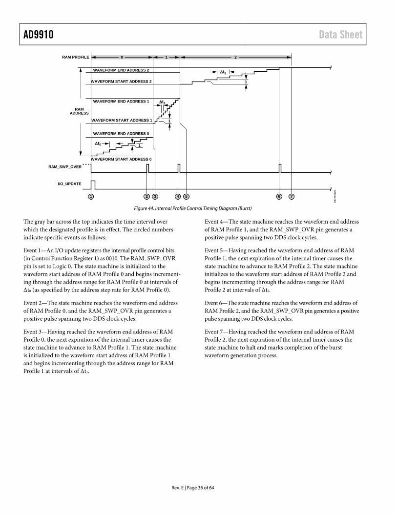
AD9910 Data Sheet
Rev. E | Page 36 of 64
RAM_SWP_OVER
WAVEFORM START ADDRESS 0
WAVEFORM END ADDRESS 0
1
WAVEFORM START ADDRESS 1
WAVEFORM END ADDRESS 1
1
WAVEFORM END ADDRESS 2
1
RAM PROFILE 0 1 2
WAVEFORM START ADDRESS 2
RAMADDRESS
I/O_UPDATE
Δt0
Δt1
Δt2
1 2 3 4 5 6 7
0647
9-02
5
Figure 44. Internal Profile Control Timing Diagram (Burst)
The gray bar across the top indicates the time interval over which the designated profile is in effect. The circled numbers indicate specific events as follows:
Event 1—An I/O update registers the internal profile control bits (in Control Function Register 1) as 0010. The RAM_SWP_OVR pin is set to Logic 0. The state machine is initialized to the waveform start address of RAM Profile 0 and begins increment-ing through the address range for RAM Profile 0 at intervals of Δt0 (as specified by the address step rate for RAM Profile 0).
Event 2—The state machine reaches the waveform end address of RAM Profile 0, and the RAM_SWP_OVR pin generates a positive pulse spanning two DDS clock cycles.
Event 3—Having reached the waveform end address of RAM Profile 0, the next expiration of the internal timer causes the state machine to advance to RAM Profile 1. The state machine is initialized to the waveform start address of RAM Profile 1 and begins incrementing through the address range for RAM Profile 1 at intervals of Δt1.
Event 4—The state machine reaches the waveform end address of RAM Profile 1, and the RAM_SWP_OVR pin generates a positive pulse spanning two DDS clock cycles.
Event 5—Having reached the waveform end address of RAM Profile 1, the next expiration of the internal timer causes the state machine to advance to RAM Profile 2. The state machine initializes to the waveform start address of RAM Profile 2 and begins incrementing through the address range for RAM Profile 2 at intervals of Δt2.
Event 6—The state machine reaches the waveform end address of RAM Profile 2, and the RAM_SWP_OVR pin generates a positive pulse spanning two DDS clock cycles.
Event 7—Having reached the waveform end address of RAM Profile 2, the next expiration of the internal timer causes the state machine to halt and marks completion of the burst waveform generation process.

Data Sheet AD9910
Rev. E | Page 37 of 64
WAVEFORM STARTADDRESS 0
WAVEFORM ENDADDRESS 0
WAVEFORM STARTADDRESS 1
WAVEFORM ENDADDRESS 1
0647
9-02
6
1
RAM_SWP_OVER
RAM PROFILE
RAMADDRESS
I/O_UPDATE
0 1 0 0 11
1 2 3 4 5 6 7 8 9 10 11
Δt0
Δt1
1
Figure 45. Internal Profile Control Timing Diagram (Continuous)
Internal Profile Control Continuous Waveform Timing Diagram
An example of an internal profile control continuous waveform timing diagram is shown in Figure 45. The diagram assumes that the internal profile control bits (in Control Function Register 1) are programmed as 1000. It also assumes that the start address in RAM Profile 1 is greater than the end address in RAM Profile 0.
The gray bar across the top indicates the time interval over which the designated profile is in effect. The circled numbers indicate specific events.
Event 1—An I/O update registers that the internal profile control bits (in Control Function Register 1) are programmed to 1000. The RAM_SWP_OVR pin is set to Logic 0. The state machine is initialized to the waveform start address of RAM Profile 0 and begins incrementing through the address range for RAM Profile 0 at intervals of Δt0 (as specified by the address step rate for RAM Profile 0).
Event 2—The state machine reaches the waveform end address of RAM Profile 0, and the RAM_SWP_OVR pin generates a positive pulse spanning two DDS clock cycles.
Event 3—Having reached the waveform end address of RAM Profile 0, the next expiration of the internal timer causes the state machine to advance to RAM Profile 1. The state machine is initialized to the waveform start address of RAM Profile 1 and begins incrementing through the address range for RAM Profile 1 at intervals of Δt1.
Event 4—The state machine reaches the waveform end address of RAM Profile 1, and the RAM_SWP_OVR pin generates a positive pulse spanning two DDS clock cycles.
Event 5—Having reached the waveform end address of RAM Profile 1, the next expiration of the internal timer causes the state machine to jump back to RAM Profile 0. The state machine initializes to the waveform start address of RAM
Profile 0 and begins incrementing through the address range for RAM Profile 0 at intervals of Δt0.
Event 5 to Event 11—These events repeat indefinitely until the internal profile control bits are reprogrammed and an I/O update is asserted.
RAM Bidirectional Ramp Mode
In bidirectional ramp mode, upon assertion of an I/O update, the RAM begins operating as a waveform generator using the parameters programmed only into RAM Profile 0 (unlike ramp up mode, which uses all eight profiles). Data is extracted from RAM over the specified address range and at the specified rate contained in the waveform start address, waveform end address, and address ramp rate values of the selected RAM profile. The data is delivered to the specified DDS signal control parameter(s) based on the RAM playback destination bits.
The PROFILE[2:1] pins are ignored by the internal logic in this mode. When a RAM profile programmed to operate in this mode is selected, no other RAM profiles can be selected until the active RAM profile is reprogrammed with a different RAM operating mode. The no-dwell high bit is ignored in this mode.
With the bidirectional ramp mode activated via an I/O update or profile change, the internal state machine readies to extract data from the RAM at the waveform start address. Data extrac-tion begins when PROFILE0 is Logic 1, which instructs the state machine to begin incrementing through the address range. As long as the PROFILE0 pin remains Logic 1, the state machine continues to extract data until it reaches the waveform end address. At this point, the state machine halts until the PROFILE0 pin is Logic 0, instructing the state machine to begin decrementing through the address range. As long as the PROFILE0 pin is Logic 0, the state machine continues to extract data until it reaches the waveform start address. At this point, the state machine halts until the PROFILE0 pin is Logic 1.

AD9910 Data Sheet
Rev. E | Page 38 of 64
0647
9-02
7
WAVEFORM START ADDRESS
WAVEFORM END ADDRESS
1
PROFILE0
RAM ADRESS
RAM_SWP_OVER
I/O_UPDATE
1 2 3 4 5 6 7 8
Δt Δt
M DDS CLOCK CYCLES
Figure 46. Bidirectional Ramp Timing Diagram
If the PROFILE0 pin changes states before the state machine reaches the programmed start or end address, the internal timer is restarted and the direction of the address counter is reversed.
Figure 46 is a graphic representation of the bidirectional ramp mode. It shows the action of the state machine in response to the PROFILE0 pin and the response of the RAM_SWP_OVR pin.
The RAM_SWP_OVR pin switches to Logic 1 when the state machine reaches the waveform end address. It remains Logic 1 until the state machine reaches the waveform start address and the PROFILE0 pin transitions from Logic 0 to Logic 1.
The circled numbers in Figure 46 indicate specific events as follows:
Event 1—An I/O update or profile change activates the RAM bidirectional ramp mode. The state machine initializes to the waveform start address, and the RAM_SWP_OVR pin is set to Logic 0.
Event 2—Pin PROFILE0 switches to Logic 1. The state machine begins incrementing the RAM address counter.
Event 3—Pin PROFILE0 remains at Logic 1 long enough for the state machine to reach the waveform end address. The RAM_ SWP_OVR pin switches to Logic 1 accordingly.
Event 4—Pin PROFILE0 switches to Logic 0. The state machine begins decrementing the RAM address counter. The RAM_ SWP_OVR pin remains at Logic 1.
Event 5—Pin PROFILE0 switches to Logic 1. The state machine resets its internal timer and reverses the direction of the RAM address counter (that is, it starts to increment). There is no change of the RAM_SWP_OVR state because the waveform start address has not yet been reached.
Event 6—Pin PROFILE0 switches to Logic 0. The state machine resets its internal timer and again reverses the direction of the RAM address counter. The RAM_SWP_OVR state does not change.
Event 7—Pin PROFILE0 remains at Logic 0 long enough for the state machine to reach the waveform start address. There is no change in the RAM_SWP_OVR state.
Event 8—Pin PROFILE0 switches to Logic 1. The state machine resets its internal timer and begins incrementing the RAM address counter. The RAM_SWP_OVR pin switches to Logic 0 because both the waveform start address was reached and the PROFILE0 pin transitioned from Logic 0 to Logic 1.
RAM Continuous Bidirectional Ramp Mode
In continuous bidirectional ramp mode, upon assertion of an I/O update or a change of profile, the RAM begins operating as a waveform generator using the parameters programmed into the RAM profile designated by the PROFILEx pins. Data is extracted from RAM over the specified address range and at the specified rate contained in the waveform start address, waveform end address, and address ramp rate values of the selected RAM profile. The data is delivered to the specified DDS signal control parameter(s) based on the RAM playback destination bits. The no-dwell high bit is ignored in this mode.
With the continuous bidirectional ramp mode activated via an I/O update or profile change, the internal state machine begins extracting data from the RAM at the waveform start address and incrementing the address counter until it reaches the waveform end address. At this point, the state machine automatically reverses the direction of the address counter and begins decrementing through the address range. Whenever one of the terminal addresses is reached, the state machine reverses the address counter; the process continues indefinitely.

Data Sheet AD9910
Rev. E | Page 39 of 64
WAVEFORM START ADDRESS
WAVEFORM END ADDRESS
1
Δt Δt
RAM ADRESS
RAM_SWP_OVER
I/O_UPDATE
M DDS CLOCK CYCLES
1 2 3 0647
9-02
8
Figure 47. Continuous Bidirectional Ramp Timing Diagram
A change in state of the PROFILE pins aborts the current wave-form, and the newly selected RAM profile is used to initiate a new waveform.
The RAM_SWP_OVR pin switches to Logic 1 when the state machine reaches the waveform end address, then returns to Logic 0 at the waveform start address, toggling each time one of these addresses is reached.
A graphic representation of the continuous bidirectional ramp mode is shown in Figure 47. The circled numbers indicate specific events as follows:
Event 1—An I/O update or profile change has activated the RAM continuous bidirectional ramp mode. The state machine initializes to the waveform start address. The RAM_SWP_OVR pin resets to Logic 0. The state machine begins incrementing through the specified address range.
Event 2—The state machine reaches the waveform end address. The RAM_SWP_OVR pin toggles to Logic 1.
Event 3—The state machine reaches the waveform start address. The RAM_SWP_OVR pin toggles to Logic 0.
The continuous bidirectional ramp continues indefinitely until the mode is changed.

AD9910 Data Sheet
Rev. E | Page 40 of 64
0647
9-02
9
WAVEFORM START ADDRESS
WAVEFORM END ADDRESS
1
1 2 3 4 5
RAM ADRESS
RAM_SWP_OVER
I/O_UPDATE
M DDS CLOCK CYCLES
∆t
Figure 48. Continuous Recirculate Timing Diagram
RAM Continuous Recirculate Mode
The continuous recirculate mode mimics the ramp-up mode, except that when the state machine reaches the waveform end address, the next timeout of the internal timer causes the state machine to jump to the waveform start address. The waveform repeats until an I/O update or profile change.
The no-dwell high bit is ignored in this mode.
A profile pin state change aborts the current waveform, and the newly selected RAM profile is used to initiate a new waveform.
The RAM_SWP_OVR pin pulses high for two DDS clock cycles when the state machine reaches the waveform end address.
Continuous recirculate mode is graphically represented in Figure 48. The circled numbers indicate specific events as follows:
Event 1—An I/O update or profile change occurs. This event initializes the state machine to the waveform start address and sets the RAM_SWP_OVR pin to Logic 0.
Event 2—The state machine reaches the waveform end address value for the selected profile. The RAM_SWP_OVR pin toggles to Logic 1 for two DDS clock cycles.
Event 3—The state machine switches to the waveform start address and continues to increment the address counter.
Event 4—The state machine again reaches the waveform end address value for the selected profile, and the RAM_SWP_OVR pin toggles to Logic 1 for two DDS clock cycles.
Event 5—The state machine switches to the waveform start address and continues to increment the address counter.
Event 4 and Event 5—These events repeat until an I/O update is issued or a change in profile is made.
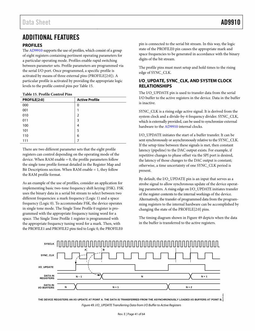
Data Sheet AD9910
Rev. E | Page 41 of 64
ADDITIONAL FEATURES PROFILES The AD9910 supports the use of profiles, which consist of a group of eight registers containing pertinent operating parameters for a particular operating mode. Profiles enable rapid switching between parameter sets. Profile parameters are programmed via the serial I/O port. Once programmed, a specific profile is activated by means of three external pins (PROFILE[2:0]). A particular profile is activated by providing the appropriate logic levels to the profile control pins per Table 15.
Table 15. Profile Control Pins PROFILE[2:0] Active Profile 000 0 001 1 010 2 011 3 100 4 101 5 110 6 111 7
There are two different parameter sets that the eight profile registers can control depending on the operating mode of the device. When RAM enable = 0, the profile parameters follow the single tone profile format detailed in the Register Map and Bit Descriptions section. When RAM enable = 1, they follow the RAM profile format.
As an example of the use of profiles, consider an application for implementing basic two-tone frequency shift keying (FSK). FSK uses the binary data in a serial bit stream to select between two different frequencies: a mark frequency (Logic 1) and a space frequency (Logic 0). To accommodate FSK, the device operates in single tone mode. The Single Tone Profile 0 register is pro-grammed with the appropriate frequency tuning word for a space. The Single Tone Profile 1 register is programmed with the appropriate frequency tuning word for a mark. Then, with the PROFILE1 and PROFILE2 pins tied to Logic 0, the PROFILE0
pin is connected to the serial bit stream. In this way, the logic state of the PROFILE0 pin causes the appropriate mark and space frequencies to be generated in accordance with the binary digits of the bit stream.
The profile pins must meet setup and hold times to the rising edge of SYNC_CLK.
I/O_UPDATE, SYNC_CLK, AND SYSTEM CLOCK RELATIONSHIPS The I/O_UPDATE pin is used to transfer data from the serial I/O buffer to the active registers in the device. Data in the buffer is inactive.
SYNC_CLK is a rising edge active signal. It is derived from the system clock and a divide-by-4 frequency divider. SYNC_CLK, which is externally provided, can be used to synchronize external hardware to the AD9910 internal clocks.
I/O_UPDATE initiates the start of a buffer transfer. It can be sent synchronously or asynchronously relative to the SYNC_CLK. If the setup time between these signals is met, then constant latency (pipeline) to the DAC output exists. For example, if repetitive changes to phase offset via the SPI port is desired, the latency of those changes to the DAC output is constant; otherwise, a time uncertainty of one SYNC_CLK period is present.
By default, the I/O_UPDATE pin is an input that serves as a strobe signal to allow synchronous update of the device operat-ing parameters. A rising edge on I/O_UPDATE initiates transfer of the register contents to the internal workings of the device. Alternatively, the transfer of programmed data from the program-ming registers to the internal hardware can be accomplished by changing the state of the PROFILE[2:0] pins.
The timing diagram shown in Figure 49 depicts when the data in the buffer is transferred to the active registers.
SYNC_CLK
SYSCLK
A B
N N + 1N – 1DATA INREGISTERS
DATA INI/O BUFFERS N N + 1 N + 2
I/O_UPDATE
THE DEVICE REGISTERS AN I/O UPDATE AT POINT A. THE DATA IS TRANSFERRED FROM THE ASYNCHRONOUSLY LOADED I/O BUFFERS AT POINT B. 0647
9-06
1
Figure 49. I/O_UPDATE Transferring Data from I/O Buffer to Active Registers

AD9910 Data Sheet
Rev. E | Page 42 of 64
AUTOMATIC I/O UPDATE The AD9910 offers an option whereby the I/O update function is asserted automatically rather than relying on an external signal supplied by the user. This feature is enabled by setting the internal I/O update active bit in Control Function Register 2 (CFR2).
When this feature is active, the I/O_UPDATE pin becomes an output pin. It generates an active high pulse each time an inter-nal I/O update occurs. The pulse width is determine by the I/O update rate control bits (CFR2[15:14]). Table 16 approximates the pulse width setting.
Table 16. Pulse Width Setting I/O Update Rate Control Bits (CFR2[15:14]) I/O Update Pulse Width 00 12 SYSCLKs 01 24 SYSCLKs 10 48 SYSCLKs 11 96 SYSCLKs
This I/O update strobe can be used to notify an external controller that the device has generated an I/O update internally.
The repetition rate of the internal I/O update is programmed via the serial I/O port. There are two parameters that control the repetition rate. The first consists of the two I/O update rate control bits in CFR2. The second is the 32-bit word in the I/O update rate register that sets the range of an internal counter. The I/O update rate control bits establish a divide-by-1, -2, -4, or -8 of a clock signal that runs at ¼ fSYSCLK. The output of the divider clocks the aforementioned 32-bit internal counter. The repetition rate of the I/O update is given by
Bf
f ASYSCLK
UPDATEOI 2_/ 2 +=
where: A is the value of the 2-bit word comprising the I/O update rate control bits. B is the value of the 32-bit word stored in the I/O update rate register.
The default value of A is 0, and the value of B is 0xFFFF. If B is programmed to 0x0003 or less, the I/O_UPDATE pin no longer pulses but assumes a static Logic 1 state.
POWER-DOWN CONTROL The AD9910 offers the ability to independently power down four specific sections of the device. Power-down functionality applies to the following:
• Digital core • DAC • Auxiliary DAC • Input REFCLK clock circuitry
A power-down of the digital core disables the ability to update the serial I/O port. However, the digital power-down bit can still be cleared via the serial port to prevent the possibility of a nonrecoverable state.
Software power-down is controlled via four independent power-down bits in Control Function Register 1 (CFR1). Software control requires that the EXT_PWR_DWN pin be forced to a Logic 0 state. In this case, setting the desired power-down bits (via the serial I/O port) powers down the associated functional block, whereas clearing the bits restores the function.
Alternatively, all four functions can be simultaneously powered down via external hardware control through the EXT_PWR_DWN pin. When this pin is forced to Logic 1, all four circuit blocks are powered down regardless of the state of the power-down bits; that is, the independent power-down bits in CFR1 are ignored and overridden when EXT_PWR_DWN is Logic 1.
Based on the state of the external power-down control bit, the EXT_PWR_DWN pin produces either a full power-down or a fast recovery power-down. The fast recovery power-down mode maintains power to the DAC bias circuitry and the PLL, VCO, and input clock circuitry. Although the fast recovery power-down does not conserve as much power as the full power-down, it allows the device to awaken very quickly from the power-down state.

Data Sheet AD9910
Rev. E | Page 43 of 64
SYNCHRONIZATION OF MULTIPLE DEVICES Multiple devices are synchronized when their clock states match and they transition between states simultaneously. Clock synchronization allows the user to asynchronously program multiple devices but synchronously activate the programming by applying a coincident I/O update to all devices
The function of the synchronization logic in the AD9910 is to force the internal clock generator to a predefined state coincident with an external synchronization signal applied to the SYNC_INx pins. If all devices are forced to the same clock state in synchro-nization with the same external signal, then the devices are, by definition, synchronized. Figure 50 is a block diagram of the synchronization function. The synchronization logic is divided into two independent blocks: a sync generator and a sync receiver, both of which use the local SYSCLK signal for internal timing.
0647
9-05
0
SYNCGENERATOR
REF_CLK
5
SYSCLK
INTERNALCLOCKS
5
4
SYNCRECEIVER
SYN
CG
ENER
ATO
REN
AB
LE
SYN
CG
ENER
ATO
RD
ELA
Y
SYN
CPO
LAR
ITY
90
91
9
10
REF_CLKINPUT
CIRCUITRY
7
8
12
SYNC_IN+
REF_CLK
SYNC_IN–
SYNC_SMP_ERR
SYNCVALIDATION
DELAY
SYNCTIMING
VALIDATIONDISABLE
CLO
CK
GEN
ERA
TOR
SETUP ANDHOLD VALIDATION
SYNCRECEIVERENABLE
SYNCRECEIVER
DELAY
INPUT DELAYAND EDGEDETECTION
SYNC_OUT+
SYNC_OUT–
Figure 50. Synchronization Circuit Block Diagram
The synchronization mechanism relies on the premise that the REFCLK signal appearing at each device is edge aligned with all others as a result of the external REFCLK distribution system (see Figure 53).
The sync generator block is shown in Figure 51. It is activated via the sync generator enable bit. It allows for one AD9910 in a group to function as a master timing source with the remaining devices slaved to the master.
SYSCLK
SYNCGENERATOR
ENABLE
SYNCGENERATOR
DELAYSYNCPOLARITY
SYNC_OUT+
SYNC_OUT–0
1
D Q
R
PROGAMMABLEDELAY÷16
5
9
10
9
10
LVDSDRIVER
0647
9-05
1
Figure 51. Sync Generator Diagram
The sync generator produces a clock signal that appears at the SYNC_OUTx pins. This clock is delivered by an LVDS driver and exhibits a 50% duty cycle. The clock has a fixed frequency given by
16_SYSCLK
OUTSYNCf
f
The clock at the SYNC_OUTx pins synchronizes with either the rising or falling edge of the internal SYSCLK signal, as determined by the sync generator polarity bit. Because the SYNC_OUTx signal is synchronized with the internal SYSCLK of the master device, the master device SYSCLK serves as the reference timing source for all slave devices. The user can adjust the output delay of the SYNC_OUTx signal in steps of ~75 ps by programming the 5-bit output sync generator delay word via the serial I/O port. The programmable output delay facilitates added edge timing flexibility to the overall synchronization mechanism.
The sync receiver block (shown in Figure 52) is activated via the sync receiver enable bit (0x0A[27]). The sync receiver consists of three subsections: the input delay and edge detection block, the internal clock generator block, and the setup and hold validation block.
The clock generator block remains operational even if the sync receiver is not enabled.

AD9910 Data Sheet
Rev. E | Page 44 of 64
LVDSRECEIVER
PROGAMMABLEDELAY
5INTERNALCLOCKS
CLOCKSTATE
SYNC PULSE
SYSCLKSETUP AND HOLD
VALIDATION
4
Q0
RESETQn
DELAYED SYNC-IN SIGNAL
SYNCRECEIVER
DELAY
SYNCRECEIVERENABLE
SYNC_SMP_ERR
7
8
12
RISING EDGEDETECTOR
ANDSTROBE
GENERATOR
SYNCTIMING
VALIDATIONDISABLE
SYNCVALIDATIONDELAY
0647
9-05
2
CLOCKGENERATOR
•••
•••
SYNC_IN+SYNC_IN–
Figure 52. Sync Receiver Diagram
SYNCIN
SYNCOUT
REF_CLKAD9910NUMBER 1 MASTER DEVICEFPGA
DATA
FPGA
DATA
FPGA
DATA
EDGEALIGNED
AT REF_CLKINPUTS
EDGEALIGNED
AT SYNC_ININPUTS.
PDC
LK
SYNCIN
SYNCOUT
REF_CLKAD9910NUMBER 2
PDC
LK
SYNCIN
SYNCOUT
REF_CLKAD9910NUMBER 3
PDC
LK
(FOR EXAMPLE AD951x)
CLOCK DISTRIBUTIONAND
DELAY EQUALIZATION
SYNCHRONIZATIONDISTRIBUTION AND
DELAY EQUALIZATION(FOR EXAMPLE AD951x)
0647
9-05
3
CLOCKSOURCE
Figure 53. Multichip Synchronization Example
The sync receiver accepts a periodic clock signal at the SYNC_ INx pins. This signal is assumed to originate from an LVDS-compatible driver. The user can delay the SYNC_INx signal in steps of ~75 ps by programming the 5-bit input sync receiver delay word in the multichip sync register. The signal at the output of the programmable delay is referred to as the delayed SYNC_INx signal.
Note that an internal 100 Ω LVDS termination resistor exists across both SYNC_IN inputs.
The edge detection logic generates a sync pulse having a dura-tion of one SYSCLK cycle with a repetition rate equal to the frequency of the signal applied to the SYNC_INx pins. The sync pulse is generated as a result of sampling the rising edge
of the delayed SYNC_INx signal with the rising edge of the local SYSCLK. The sync pulse is routed to the internal clock generator, which behaves as a presettable counter clocked at the SYSCLK rate. The sync pulse presets the counter to a predefined state (programmable via the 6-bit sync state preset value word in the multichip sync register). The predefined state is only active for a single SYSCLK cycle, after which the clock generator resumes cycling through its state sequence at the SYSCLK rate. This unique state presetting mechanism gives the user the flexibility to synchronize devices with specific relative clock state offsets (by assigning a different sync state preset value word to each device).
Multiple device synchronization is accomplished by providing each AD9910 with a SYNC_INx signal that is edge aligned

Data Sheet AD9910
Rev. E | Page 45 of 64
across all the devices. If the SYNC_INx signal is edge aligned at all devices, and all devices have the same sync receiver delay and sync state preset value, then they all have matching clock states (that is, they are synchronized). This concept is shown in Figure 53, in which three AD9910 devices are synchronized, with one device operating as a master timing unit and the others as slave units.
The master device must have its SYNC_INx pins included as part of the synchronization distribution and delay equalization mecha-nism in order for it to be synchronized with the slave units.
The synchronization mechanism begins with the clock distribu-tion and delay equalization block, which is used to ensure that all devices receive an edge-aligned REFCLK signal. However, even though the REFCLK signal is edge aligned among all devices, this alone does not guarantee that the clock state of each internal clock generator is coordinated with the others. This is the role of the synchronization and delay equalization block. This block accepts the SYNC_OUTx signal generated by the master device and redistributes it to the SYNC_INx input of the slave units (as well as feeding it back to the master). The goal of the redistributed SYNC_OUT x signal from the master device is to deliver an edge-aligned SYNC_INx signal to all of the sync receivers.
Assuming that all devices share the same REFCLK edge (due to the clock distribution and delay equalization block), and all devices share the same SYNC_INx edge (due to the synchroni-zation and delay equalization block), then all devices should generate an internal sync pulse in unison (assuming that they all have the same sync receiver delay value). With the further stipulation that all devices have the same sync state preset value, then the synchronized sync pulses cause all of the devices to
assume the same predefined clock state simultaneously; that is, the internal clocks of all devices become fully synchronized.
The synchronization mechanism depends on the reliable gen-eration of a sync pulse by the edge detection block in the sync receiver. Generation of a valid sync pulse, however, requires proper sampling of the rising edge of the delayed SYNC_INx signal with the rising edge of the local SYSCLK. If the edge timing of these signals fails to meet the setup or hold time requirements of the internal latches in the edge detection circuitry, then the proper generation of the sync pulse is in jeopardy. The setup and hold validation block (see Figure 54) gives the user a means to validate that proper edge timing exists between the two signals.
The setup and hold validation block can be disabled via the sync timing validation disable bit in Control Function Register 2.
The validation block makes use of a user-specified time window (programmable in increments of ~75 ps via the 4-bit sync validation delay word in the multichip sync register). The setup validation and hold validation circuits use latches identical to those in the rising edge detector and strobe generator. The programmable time window is used to skew the timing between the rising edges of the local SYSCLK signal and the rising edges of the delayed SYNC_INx signal. If either the hold or setup validation circuits fail to detect a valid edge sample, the condition is indicated externally via the SYNC_SMP_ERR pin (active high).
The user must choose a sync validation delay value that is a reasonable fraction of the SYSCLK period. For example, if the SYSCLK frequency is 1 GHz (1 ns period), then a reasonable value is 4 (300 ps). Choosing too large a value can cause the SYNC_SMP_ERR pin to generate false error signals. Choosing too small a value may cause instability.
SYNCPULSE
SYSCLK
DELAY
DELAY
CH
ECK
LO
GIC
4SYNC VALIDATIONDELAY4
4 SYNC_SMP_ERR
SYNC RECEIVER
12
SYNC TIMING VALIDATION DISABLE
SETUPVALIDATION
HOLDVALIDATION
D Q
12
SETUP AND HOLD VALIDATION
TOCLOCKGENERATIONLOGIC
FROMSYNC
RECEIVERDELAYLOGIC
D Q
D Q
RISING EDGEDETECTOR
AND STROBEGENERATOR
0647
9-05
4
Figure 54. Sync Timing Validation Block

AD9910 Data Sheet
Rev. E | Page 46 of 64
POWER SUPPLY PARTITIONING The AD9910 features multiple power supplies, and their power consumption varies with its configuration. This section covers which power supplies can be grouped together and how the power consumption of each block varies with frequency.
The values quoted in this section are for comparison only. Refer to Table 1 for exact values. With each group, use 0.1 μF or 0.01 μF bypass capacitors in parallel with a 10 μF capacitor.
The recommendations here are for typical applications, for which there are four groups of power supplies: 3.3 V digital, 3.3 V analog, 1.8 V digital, and 1.8 V analog.
Applications demanding the highest performance may require additional power supply isolation.
3.3 V SUPPLIES DVDD_I/O (3.3 V) (Pin 11, Pin 15, Pin 21, Pin 28, Pin 45, Pin 56, and Pin 66)
These 3.3 V supplies can be grouped together. The power consumption on these pins varies dynamically with serial port activity.
AVDD (3.3 V) (Pin 74 to Pin 77 and Pin 83)
These are 3.3 V DAC power supplies that typically consume about 28 mA. At a minimum, a ferrite bead should be used to isolate these from other 3.3 V supplies, with a separate regulator being ideal. The current consumption of these supplies consist mainly of biasing current and do not vary with frequency.
1.8 V SUPPLIES DVDD (1.8 V) (Pin 17, Pin 23, Pin 30, Pin 47, Pin 57, and Pin 64)
These pins can be grouped together. Their current consumption increases linearly with the system clock frequency. See Figure 17 and Figure 18 for typical current consumption curves. There is also a slight (~5%) increase as fOUT increases from 50 MHz to 400 MHz.
AVDD (1.8 V) (Pin 3)
This 1.8 V supply powers the REFCLK multiplier (PLL) and consumes about 7 mA. For applications demanding the highest performance with the PLL enabled, this supply should be isolated from other 1.8 V AVDD supplies with a separate regulator. For less demanding applications, this supply can be run off the same regulator as Pin 89 and Pin 92 with a ferrite bead to isolate Pin 3 from Pin 89 and Pin 92.
The loop filter for the PLL should directly connect to Pin 3. If the PLL is bypassed, Pin 3 should still be powered, but isolation is not critical.
AVDD (1.8 V) (Pin 6)
This pin can be grouped together with the DVDD 1.8 V supply pins. For the highest performance, a ferrite bead should be used for isolation, with a separate regulator being ideal.
AVDD (1.8 V) (Pin 89 and Pin 92)
This 1.8 V supply for the REFCLK input consumes about 15 mA. These pins can run off the supply of Pin 3 with a ferrite bead to isolate Pin 3 from Pin 89 and Pin 92. At a minimum, a ferrite bead should be used to isolate these from other 1.8 V supplies. However, for applications demanding the highest performance, a separate regulator is recommended.

Data Sheet AD9910
Rev. E | Page 47 of 64
SERIAL PROGRAMMING CONTROL INTERFACE—SERIAL I/O The AD9910 serial port is a flexible, synchronous serial commu-nications port allowing easy interface to many industry-standard microcontrollers and microprocessors. The serial I/O is compatible with most synchronous transfer formats.
The interface allows read/write access to all registers that configure the AD9910. MSB-first or LSB-first transfer formats are supported. In addition, the serial interface port can be configured as a single pin input/output (SDIO) allowing a 2-wire interface, or it can be configured as two unidirectional pins for input/output (SDIO/SDO) enabling a 3-wire interface. Two optional pins (I/O_RESET and CS) enable greater flexibility for designing systems with the AD9910.
GENERAL SERIAL I/O OPERATION There are two phases to a serial communications cycle. The first is the instruction phase to write the instruction byte into the AD9910. The instruction byte contains the address of the register to be accessed (see the Register Map and Bit Descriptions section) and defines whether the upcoming data transfer is a write or read operation.
For a write cycle, Phase 2 represents the data transfer between the serial port controller to the serial port buffer. The number of bytes transferred is a function of the register being accessed. For example, when accessing the Control Function Register 2 (Address 0x01), Phase 2 requires that four bytes be transferred. Each bit of data is registered on each corresponding rising edge of SCLK. The serial port controller expects that all bytes of the register be accessed; otherwise, the serial port controller is put out of sequence for the next communication cycle. However, one way to write fewer bytes than required is to use the I/O_RESET pin feature. The I/O_RESET pin function can be used to abort an I/O operation and reset the pointer of the serial port con-troller. After an I/O reset, the next byte is the instruction byte. Note that every completed byte written prior to an I/O reset is preserved in the serial port buffer. Partial bytes written are not preserved. At the completion of any communication cycle, the AD9910 serial port controller expects the next eight rising SCLK edges to be the instruction byte for the next communi-cation cycle.
After a write cycle, the programmed data resides in the serial port buffer and is inactive. I/O_UPDATE transfers data from the serial port buffer to active registers. The I/O update can be sent either after each communication cycle or when all serial operations are complete. In addition, a change in profile pins can initiate an I/O update.
For a read cycle, Phase 2 is the same as the write cycle with the following differences: data is read from the active registers, not
the serial port buffer, and data is driven out on the falling edge of SCLK.
Note that to read back any profile register (0x0E to 0x15), the three external profile pins must be used. For example, if the profile register is Profile 5 (0x13), then the PROFILE[0:2] pins must equal 101.This is not required to write to profile registers.
INSTRUCTION BYTE The instruction byte contains the following information as shown in the instruction byte information bit map.
Instruction Byte Information Bit Map
MSB LSB
D7 D6 D5 D4 D3 D2 D1 D0
R/W X X A4 A3 A2 A1 A0
R/W—Bit 7 of the instruction byte determines whether a read or write data transfer occurs after the instruction byte write. Logic 1 indicates a read operation. Cleared indicates a write operation.
X, X—Bit 6 and Bit 5 of the instruction byte are don’t cares.
A4, A3, A2, A1, A0—Bit 4, Bit 3, Bit 2, Bit 1, and Bit 0 of the instruction byte determine which register is accessed during the data transfer portion of the communications cycle.
SERIAL I/O PORT PIN DESCRIPTIONS SCLK—Serial Clock
The serial clock pin is used to synchronize data to and from the AD9910 and to run the internal state machines.
CS—Chip Select Bar
CS is an active low input that allows more than one device on the same serial communications line. The SDO and SDIO pins go to a high impedance state when this input is high. If driven high during any communications cycle, that cycle is suspended until CS is reactivated low. Chip select (CS) can be tied low in systems that maintain control of SCLK.
SDIO—Serial Data Input/Output
Data is always written into the AD9910 on this pin. However, this pin can be used as a bidirectional data line. Bit 1 of CFR1 Register Address 0x00 controls the configuration of this pin. The default is cleared, which configures the SDIO pin as bidirectional.
SDO—Serial Data Out
Data is read from this pin for protocols that use separate lines for transmitting and receiving data. When the AD9910 operates in single bidirectional I/O mode, this pin does not output data and is set to a high impedance state.

AD9910 Data Sheet
Rev. E | Page 48 of 64
I/O_RESET—Input/Output Reset
I/O_RESET synchronizes the I/O port state machines without affecting the contents of the addressable registers. An active high input on the I/O_RESET pin causes the current communica-tion cycle to abort. After I/O_RESET returns low (Logic 0), another communication cycle can begin, starting with the instruction byte write.
I/O_UPDATE—Input/Output Update
The I/O_UPDATE initiates the transfer of written data from the I/O port buffer to active registers. I/O_UPDATE is active on the rising edge, and its pulse width must be greater than one SYNC_CLK period. It is either an input or output pin depending on the programming of the internal I/O update active bit.
SERIAL I/O TIMING DIAGRAMS Figure 55 through Figure 58 provide basic examples of the timing relationships between the various control signals of the serial I/O port. Most of the bits in the register map are not transferred to their internal destinations until assertion of an I/O update, which is not included in the timing diagrams that follow.
MSB/LSB TRANSFERS The AD9910 serial port can support both most significant bit (MSB) first or least significant bit (LSB) first data formats. This functionality is controlled by Bit 0 in Control Function Register 1 (0x00). The default format is MSB first. If LSB first is active, all data, including the instruction byte, must follow LSB-first conven-tion. Note that the highest number found in the bit range column for each register is the MSB, and the lowest number is the LSB for that register (see the Register Map and Bit Descriptions section and Table 17).
I7SDIO
INSTRUCTION CYCLE DATA TRANSFER CYCLE
SCLK
CS
I6 I5 I4 I3 I2 I1 I0 D7 D6 D5 D4 D3 D2 D1 D0
0647
9-03
0
Figure 55. Serial Port Write Timing, Clock Stall Low
DO7
INSTRUCTION CYCLE DATA TRANSFER CYCLE
DON'T CAREI7 I6 I5 I4 I3 I2 I1 I0SDIO
SCLK
CS
SDO DO6 DO5 DO4 DO3 DO2 DO1 DO0
0647
9-03
1
Figure 56. 3-Wire Serial Port Read Timing, Clock Stall Low
I7SDIO
INSTRUCTION CYCLE DATA TRANSFER CYCLE
SCLK
CS
I6 I5 I4 I3 I2 I1 I0 D7 D6 D5 D4 D3 D2 D1 D0
0647
9-03
2
Figure 57. Serial Port Write Timing, Clock Stall High
I7SDIO
INSTRUCTION CYCLE DATA TRANSFER CYCLE
SCLK
CS
I6 I5 I4 I3 I2 I1 I0 DO7 DO6 DO5 DO4 DO3 DO2 DO1 DO0
0647
9-03
3
Figure 58. 2-Wire Serial Port Read Timing, Clock Stall High

Data Sheet AD9910
Rev. E | Page 49 of 64
REGISTER MAP AND BIT DESCRIPTIONS Table 17. Register Map Register Name (Serial Address)
Bit Range (Internal Address)
Bit 7 (MSB) Bit 6 Bit 5 Bit 4 Bit 3 Bit 2 Bit 1 Bit 0 (LSB)
Default Value1 (Hex)
CFR1—Control Function Register 1 (0x00)
31:24 RAM enable
RAM playback destination
Open 0x00
23:16 Manual OSK external control
Inverse sinc filter enable
Open Internal profile control Select DDS sine output
0x00
15:8 Load LRR @ I/O update
Autoclear digital ramp accumu-lator
Autoclear phase accumu-lator
Clear digital ramp accumu-lator
Clear phase accumu-lator
Load ARR @ I/O update
OSK enable
Select auto OSK
0x00
7:0 Digital power-down
DAC power-down
REFCLK input power-down
Aux DAC power-down
External power-down control
Open SDIO input only
LSB first 0x00
CFR2—Control Function Register 2 (0x01)
31:24 Open Enable amplitude scale from single tone profiles
0x00
23:16 Internal I/O update active
SYNC_CLK enable
Digital ramp destination Digital ramp enable
Digital ramp no-dwell high
Digital ramp no-dwell low
Read effective FTW
0x40
15:8 I/O update rate control Open PDCLK enable
PDCLK invert
TxEnable invert
Open 0x08
7:0 Matched latency enable
Data assembler hold last value
Sync timing validation disable
Parallel data port enable
FM gain 0x20
CFR3—Control Function Register 3 (0x02)
31:24 Open DRV0[1:0] Open VCO SEL[2:0] 0x1F
23:16 Open ICP[2:0] Open 0x3F
15:8 REFCLK input divider bypass
REFCLK input divider ResetB
Open PFD reset Open PLL enable 0x40
7:0 N[6:0] Open 0x00
Auxiliary DAC Control (0x03)
31:24 Open 0x00
23:16 Open 0x00
15:8 Open 0x00
7:0 FSC[7:0] 0x7F
I/O Update Rate (0x04)
31:24 I/O update rate[31:24] 0xFF
23:16 I/O update rate[23:16] 0xFF
15:8 I/O update rate[15:8] 0xFF
7:0 I/O update rate[7:0] 0xFF
FTW—Frequency Tuning Word (0x07)
31:24 Frequency tuning word[31:24] 0x00
23:16 Frequency tuning word[23:16] 0x00
15:8 Frequency tuning word[15:8] 0x00
7:0 Frequency tuning word[7:0] 0x00

AD9910 Data Sheet
Rev. E | Page 50 of 64
Register Name (Serial Address)
Bit Range (Internal Address)
Bit 7 (MSB) Bit 6 Bit 5 Bit 4 Bit 3 Bit 2 Bit 1 Bit 0 (LSB)
Default Value1 (Hex)
POW—Phase Offset Word (0x08)
15:8 Phase offset word[15:8] 0x00
7:0 Phase offset word[7:0] 0x00
ASF—Amplitude Scale Factor (0x09)
31:24 Amplitude ramp rate[15:8] 0x00
23:16 Amplitude ramp rate[7:0] 0x00
15:8 Amplitude scale factor[13:6] 0x00
7:0 Amplitude scale factor[5:0] Amplitude step size[1:0] 0x00
Multichip Sync (0x0A)
31:24 Sync validation delay[3:0] Sync receiver enable
Sync generator enable
Sync generator polarity
Open 0x00
23:16 Sync state preset value[5:0] Open 0x00
15:8 Output sync generator delay[4:0] Open 0x00
7:0 Input sync receiver delay[4:0] Open 0x00 Digital Ramp Limit (0x0B)
63:56 Digital ramp upper limit[31:24] N/A
55:48 Digital ramp upper limit[23:16] N/A
47:40 Digital ramp upper limit[15:8] N/A
39:32 Digital ramp upper limit[7:0] N/A
31:24 Digital ramp lower limit[31:24] N/A
23:16 Digital ramp lower limit[23:16] N/A
15:8 Digital ramp lower limit[15:8] N/A
7:0 Digital ramp lower limit[7:0] N/A
Digital Ramp Step Size (0x0C)
63:56 Digital ramp decrement step size[31:24] N/A
55:48 Digital ramp decrement step size[23:16] N/A
47:40 Digital ramp decrement step size[15:8] N/A
39:32 Digital ramp decrement step size[7:0] N/A
31:24 Digital ramp increment step size[31:24] N/A
23:16 Digital ramp increment step size[23:16] N/A
15:8 Digital ramp increment step size[15:8] N/A
7:0 Digital ramp increment step size[7:0] N/A
Digital Ramp Rate (0x0D)
31:24 Digital ramp negative slope rate [15:8] N/A
23:16 Digital ramp negative slope rate[7:0] N/A 15:8 Digital ramp positive slope rate[15:8] N/A
7:0 Digital ramp positive slope rate[7:0] N/A
Single Tone Profile 0 (0x0E)
63:56 Open Amplitude Scale Factor 0[13:8] 0x08
55:48 Amplitude Scale Factor 0[7:0] 0xB5
47:40 Phase Offset Word 0[15:8] 0x00
39:32 Phase Offset Word 0[7:0] 0x00
31:24 Frequency Tuning Word 0[31:24] 0x00
23:16 Frequency Tuning Word 0[23:16] 0x00
15:8 Frequency Tuning Word 0[15:8] 0x00
7:0 Frequency Tuning Word 0[7:0] 0x00

Data Sheet AD9910
Rev. E | Page 51 of 64
Register Name (Serial Address)
Bit Range (Internal Address)
Bit 7 (MSB) Bit 6 Bit 5 Bit 4 Bit 3 Bit 2 Bit 1 Bit 0 (LSB)
Default Value1 (Hex)
RAM Profile 0 (0x0E)
63:56 Open 0x00
55:48 RAM Profile 0 address step rate[15:8] 0x00
47:40 RAM Profile 0 address step rate[7:0] 0x00
39:32 RAM Profile 0 waveform end address[9:2] 0x00
31:24 RAM Profile 0 waveform end address[1:0]
Open 0x00
23:16 RAM Profile 0 waveform start address[9:2] 0x00
15:8 RAM Profile 0 waveform start address[1:0]
Open 0x00
7:0 Open No-dwell high
Open Zero-crossing
RAM Profile 0 mode control[2:0] 0x00
Single Tone Profile 1 (0x0F)
63:56 Open Amplitude Scale Factor 1[13:8] 0x00
55:48 Amplitude Scale Factor 1[7:0] 0x00
47:40 Phase Offset Word 1[15:8] 0x00
39:32 Phase Offset Word 1[7:0] 0x00
31:24 Frequency Tuning Word 1[31:24] 0x00
23:16 Frequency Tuning Word 1[23:16] 0x00 15:8 Frequency Tuning Word 1[15:8] 0x00
7:0 Frequency Tuning Word 1[7:0] 0x00
RAM Profile 1 (0x0F)
63:56 Open 0x00
55:48 RAM Profile 1 address step rate[15:8] 0x00
47:40 RAM Profile 1 address step rate[7:0] 0x00
39:32 RAM Profile 1 waveform end address[9:2] 0x00
31:24 RAM Profile 1 waveform end address[1:0]
Open 0x00
23:16 RAM Profile 1 waveform start address[9:2] 0x00
15:8 RAM Profile 1 waveform start address[1:0]
Open 0x00
7:0 Open No-dwell high
Open Zero- crossing
RAM Profile 1 mode control[2:0] 0x00
Single Tone Profile 2 (0x10)
63:56 Open Amplitude Scale Factor 2[13:8] 0x00
55:48 Amplitude Scale Factor 2[7:0] 0x00
47:40 Phase Offset Word 2[15:8] 0x00
39:32 Phase Offset Word 2[7:0] 0x00
31:24 Frequency Tuning Word 2[31:24] 0x00
23:16 Frequency Tuning Word 2[23:16] 0x00
15:8 Frequency Tuning Word 2[15:8] 0x00
7:0 Frequency Tuning Word 2[7:0] 0x00
RAM Profile 2 (0x10)
63:56 Open 0x00
55:48 RAM Profile 2 address step rate[15:8] 0x00
47:40 RAM Profile 2 address step rate[7:0] 0x00
39:32 RAM Profile 2 waveform end address[9:2] 0x00
31:24 RAM Profile 2 waveform end address[1:0]
Open 0x00
23:16 RAM Profile 2 waveform start address[9:2] 0x00
15:8 RAM Profile 2 waveform start address[1:0]
Open 0x00
7:0 Open No-dwell high
Open Zero-crossing
RAM Profile 2 mode control[2:0] 0x00

AD9910 Data Sheet
Rev. E | Page 52 of 64
Register Name (Serial Address)
Bit Range (Internal Address)
Bit 7 (MSB) Bit 6 Bit 5 Bit 4 Bit 3 Bit 2 Bit 1 Bit 0 (LSB)
Default Value1 (Hex)
Single Tone Profile 3 (0x11)
63:56 Open Amplitude Scale Factor 3[13:8] 0x00
55:48 Amplitude Scale Factor 3[7:0] 0x00
47:40 Phase Offset Word 3[15:8] 0x00
39:32 Phase Offset Word 3[7:0] 0x00
31:24 Frequency Tuning Word 3[31:24] 0x00
23:16 Frequency Tuning Word 3[23:16] 0x00
15:8 Frequency Tuning Word 3[15:8] 0x00
7:0 Frequency Tuning Word 3[7:0] 0x00 RAM Profile 3 (0x11)
63:56 Open 0x00
55:48 RAM Profile 3 address step rate[15:8] 0x00
47:40 RAM Profile 3 address step rate[7:0] 0x00
39:32 RAM Profile 3 waveform end address[9:2] 0x00
31:24 RAM Profile 3 waveform end address[1:0]
Open 0x00
23:16 RAM Profile 3 waveform start address[9:2] 0x00
15:8 RAM Profile 3 waveform start address[1:0]
Open 0x00
7:0 Open No-dwell high
Open Zero-crossing
RAM Profile 3 mode control[2:0] 0x00
Single Tone Profile 4 (0x12)
63:56 Open Amplitude Scale Factor 4[13:8] 0x00
55:48 Amplitude Scale Factor 4[7:0] 0x00
47:40 Phase Offset Word 4[15:8] 0x00
39:32 Phase Offset Word 4[7:0] 0x00
31:24 Frequency Tuning Word 4[31:24] 0x00
23:16 Frequency Tuning Word 4[23:16] 0x00
15:8 Frequency Tuning Word 4[15:8] 0x00
7:0 Frequency Tuning Word 4[7:0] 0x00
RAM Profile 4 (0x12)
63:56 Open 0x00
55:48 RAM Profile 4 address step rate[15:8] 0x00
47:40 RAM Profile 4 address step rate[7:0] 0x00
39:32 RAM Profile 4 waveform end address[9:2] 0x00
31:24 RAM Profile 4 waveform end address[1:0]
Open 0x00
23:16 RAM Profile 4 waveform start address[9:2] 0x00
15:8 RAM Profile 4 waveform start address[1:0]
Open 0x00
7:0 Open No-dwell high
Open Zero-crossing
RAM Profile 4 mode control[2:0] 0x00
Single Tone Profile 5 (0x13)
63:56 Open Amplitude Scale Factor 5[13:8] 0x00
55:48 Amplitude Scale Factor 5[7:0] 0x00
47:40 Phase Offset Word 5[15:8] 0x00
39:32 Phase Offset Word 5[7:0] 0x00
31:24 Frequency Tuning Word 5[31:24] 0x00
23:16 Frequency Tuning Word 5[23:16] 0x00
15:8 Frequency Tuning Word 5[15:8] 0x00 7:0 Frequency Tuning Word 5[7:0] 0x00

Data Sheet AD9910
Rev. E | Page 53 of 64
Register Name (Serial Address)
Bit Range (Internal Address)
Bit 7 (MSB) Bit 6 Bit 5 Bit 4 Bit 3 Bit 2 Bit 1 Bit 0 (LSB)
Default Value1 (Hex)
RAM Profile 5 (0x13)
63:56 Open 0x00
55:48 RAM Profile 5 address step rate[15:8] 0x00
47:40 RAM Profile 5 address step rate[7:0] 0x00
39:32 RAM Profile 5 waveform end address[9:2] 0x00
31:24 RAM Profile 5 waveform end address[1:0]
Open 0x00
23:16 RAM Profile 5 waveform start address[9:2] 0x00
15:8 RAM Profile 5 waveform start address[1:0]
Open 0x00
7:0 Open No-dwell high
Open Zero-crossing
RAM Profile 5 mode control[2:0] 0x00
Single Tone Profile 6 (0x14)
63:56 Open Amplitude Scale Factor 6[13:8] 0x00
55:48 Amplitude Scale Factor 6[7:0] 0x00
47:40 Phase Offset Word 6[15:8] 0x00
39:32 Phase Offset Word 6[7:0] 0x00
31:24 Frequency Tuning Word 6[31:24] 0x00
23:16 Frequency Tuning Word 6[23:16] 0x00 15:8 Frequency Tuning Word 6[15:8] 0x00
7:0 Frequency Tuning Word 6[7:0] 0x00
RAM Profile 6 (0x14)
63:56 Open 0x00
55:48 RAM Profile 6 address step rate[15:8] 0x00
47:40 RAM Profile 6 address step rate[7:0] 0x00
39:32 RAM Profile 6 waveform end address[9:2] 0x00
31:24 RAM Profile 6 waveform end address[1:0]
Open 0x00
23:16 RAM Profile 6 waveform start address[9:2] 0x00
15:8 AM Profile 6 waveform start address[1:0]
Open 0x00
7:0 Open No-dwell high
Open Zero-crossing
RAM Profile 6 mode control[2:0] 0x00
Single Tone Profile 7 (0x15)
63:56 Open Amplitude Scale Factor 7[13:8] 0x00
55:48 Amplitude Scale Factor 7[7:0] 0x00
47:40 Phase Offset Word 7[15:8] 0x00
39:32 Phase Offset Word 7[7:0] 0x00
31:24 Frequency Tuning Word 7[31:24] 0x00
23:16 Frequency Tuning Word 7[23:16] 0x00
15:8 Frequency Tuning Word 7[15:8] 0x00
7:0 Frequency Tuning Word 7[7:0] 0x00
RAM Profile 7 (0x15)
63:56 Open 0x00
55:48 RAM Profile 7 address step rate[15:8] 0x00
47:40 RAM Profile 7 address step rate[7:0] 0x00
39:32 RAM Profile 7 waveform end address[9:2] 0x00
31:24 RAM Profile 7 waveform end address[1:0]
Open 0x00
23:16 RAM Profile 7 waveform start address[9:2] 0x00
15:8 RAM Profile 7 waveform start address[1:0]
Open 0x00
7:0 Open No-dwell high
Open Zero-crossing
RAM Profile 7 mode control[2:0] 0x00
RAM (0x16) 31:0 RAM word[31:0] 0x00 1 N/A = not applicable.

AD9910 Data Sheet
Rev. E | Page 54 of 64
REGISTER BIT DESCRIPTIONS The serial I/O port registers span an address range of 0 to 23 (0x00 to 0x16 in hexadecimal notation). This represents a total of 24 registers. However, two of these registers are unused, yielding a total of 22 available registers. The unused registers are Register 5 and Register 6 (0x05 and 0x06, respectively).
The number of bytes assigned to the registers varies. That is, the registers are not of uniform depth; each contains the number of bytes necessary for its particular function. Additionally, the registers are assigned names according to their functionality. In some cases, a register is given a mnemonic descriptor. For example, the register at Serial Address 0x00 is named Control Function Register 1 and is assigned the mnemonic CFR1.
The following section provides a detailed description of each bit in the AD9910 register map. For cases in which a group of bits serves a specific function, the entire group is considered a binary word and described in aggregate.
This section is organized in sequential order of the serial addresses of the registers. Each subheading includes the register name and optional register mnemonic (in parentheses). Also given is the serial address in hexadecimal format and the number of bytes assigned to the register.
Following each subheading is a table containing the individual bit descriptions for that particular register. The location of the bit(s) in the register is indicated by a single number or a pair of numbers separated by a colon; that is, a pair of numbers (A:B) indicates a range of bits from the most significant (A) to the least significant (B). For example, 5:2 implies Bit Position 5 down to Bit Position 2, inclusive, with Bit 0 identifying the LSB of the register.
Unless otherwise stated, programmed bits are not transferred to their internal destinations until the assertion of the I/O_UPDATE pin or a profile change.
Control Function Register 1 (CFR1)—Address 0x00
Four bytes are assigned to this register.
Table 18. Bit Description for CFR1 Bit(s) Mnemonic Description 31 RAM enable 0 = disables RAM functionality (default). 1 = enables RAM functionality (required for both load/retrieve and playback operation). 30:29 RAM playback destination See Table 12 for details; default is 00b. 28:24 Open 23 Manual OSK external
control Ineffective unless CFR1[9:8] = 10b.
0 = OSK pin inoperative (default). 1 = OSK pin enabled for manual OSK control (see Output Shift Keying (OSK) section for
details). 22 Inverse sinc filter enable 0 = inverse sinc filter bypassed (default). 1 = inverse sinc filter active. 21 Open 20:17 Internal profile control Ineffective unless CFR1[31] = 1. These bits are effective without the need for an I/O update.
See Table 14 for details. Default is 0000b. 16 Select DDS sine output 0 = cosine output of the DDS is selected (default). 1 = sine output of the DDS is selected. 15 Load LRR @ I/O update Ineffective unless CFR2[19] = 1. 0 = normal operation of the digital ramp timer (default). 1 = digital ramp timer loaded any time I/O_UPDATE is asserted or a PROFILE[2:0] change
occurs. 14 Autoclear digital ramp
accumulator 0 = normal operation of the DRG accumulator (default). 1 = the ramp accumulator is reset for one cycle of the DDS clock after which the accumula-tor automatically resumes normal operation. As long as this bit remains set, the ramp accumulator is momentarily reset each time an I/O_UPDATE is asserted or a PROFILE[2:0] change occurs. This bit is synchronized with either an I/O _UPDATE or a PROFILE[2:0] change and the next rising edge of SYNC_CLK.
13 Autoclear phase accumulator
0 = normal operation of the DDS phase accumulator (default). 1 = synchronously resets the DDS phase accumulator anytime I/O_UPDATE is asserted or a profile change occurs.

Data Sheet AD9910
Rev. E | Page 55 of 64
Bit(s) Mnemonic Description 12 Clear digital ramp
accumulator 0 = normal operation of the DRG accumulator (default). 1 = asynchronous, static reset of the DRG accumulator. The ramp accumulator remains reset as long as this bit remains set. This bit is synchronized with either an I/O_UPDATE or a PROFILE[2:0] change and the next rising edge of SYNC_CLK.
11 Clear phase accumulator 0 = normal operation of the DDS phase accumulator (default). 1 = asynchronous, static reset of the DDS phase accumulator. 10 Load ARR @ I/O update Ineffective unless CFR1[9:8] = 11b. 0 = normal operation of the OSK amplitude ramp rate timer (default). 1 = OSK amplitude ramp rate timer reloaded anytime I/O_UPDATE is asserted or a
PROFILE[2:0] change occurs. 9 OSK enable The output shift keying enable bit. 0 = OSK disabled (default). 1 = OSK enabled. 8 Select auto OSK Ineffective unless CFR1[9] = 1. 0 = manual OSK enabled (default). 1 = automatic OSK enabled. 7 Digital power-down This bit is effective without the need for an I/O update. 0 = clock signals to the digital core are active (default). 1 = clock signals to the digital core are disabled. 6 DAC power-down 0 = DAC clock signals and bias circuits are active (default). 1 = DAC clock signals and bias circuits are disabled. 5 REFCLK input power-down This bit is effective without the need for an I/O update. 0 = REFCLK input circuits and PLL are active (default). 1 = REFCLK input circuits and PLL are disabled. 4 Auxiliary DAC power-down 0 = auxiliary DAC clock signals and bias circuits are active (default). 1 = auxiliary DAC clock signals and bias circuits are disabled. 3 External power-down
control 0 = assertion of the EXT_PWR_DWN pin affects full power-down (default).
1 = assertion of the EXT_PWR_DWN pin affects fast recovery power-down. 2 Open 1 SDIO input only 0 = configures the SDIO pin for bidirectional operation; 2-wire serial programming
mode (default). 1 = configures the serial data I/O pin (SDIO) as an input only pin; 3-wire serial
programming mode. 0 LSB first 0 = configures the serial I/O port for MSB-first format (default). 1 = configures the serial I/O port for LSB-first format.

AD9910 Data Sheet
Rev. E | Page 56 of 64
Control Function Register 2 (CFR2)—Address 0x01
Four bytes are assigned to this register.
Table 19. Bit Descriptions for CFR2 Bit(s) Mnemonic Description 31:25 Open 24 Enable amplitude scale
from single tone profiles Ineffective if CFR2[19 ] = 1 or CFR1[31] = 1 or CFR1[9] = 1.
0 = the amplitude scaler is bypassed and shut down for power conservation (default). 1 = the amplitude is scaled by the ASF from the active profile. 23 Internal I/O update active This bit is effective without the need for an I/O update.
0 = serial I/O programming is synchronized with the external assertion of the I/O_UPDATE pin, which is configured as an input pin (default). 1 = serial I/O programming is synchronized with an internally generated I/O update signal (the internally generated signal appears at the I/O_UPDATE pin, which is configured as an output pin).
22 SYNC_CLK enable 0 = the SYNC_CLK pin is disabled; static Logic 0 output. 1 = the SYNC_CLK pin generates a clock signal at ¼ fSYSCLK; used for synchronization of the
serial I/O port (default). 21:20 Digital ramp destination See Table 11 for details. Default is 00b. See the Digital Ramp Generator (DRG) section for
details. 19 Digital ramp enable 0 = disables digital ramp generator functionality (default). 1 = enables digital ramp generator functionality. 18 Digital ramp no-dwell high See the Digital Ramp Generator (DRG) section for details. 0 = disables no-dwell high functionality (default). 1 = enables no-dwell high functionality. 17 Digital ramp no-dwell low See the Digital Ramp Generator (DRG) section for details. 0 = disables no-dwell low functionality (default). 1 = enables no-dwell low functionality. 16 Read effective FTW 0 = a serial I/O port read operation of the FTW register reports the contents of the FTW
register (default). 1 = a serial I/O port read operation of the FTW register reports the actual 32-bit word
appearing at the input to the DDS phase accumulator. 15:14 I/O update rate control Ineffective unless CFR2[23] = 1. Sets the prescale ratio of the divider that clocks the auto I/O
update timer as follows: 00 = divide-by-1 (default). 01 = divide-by-2. 10 = divide-by-4. 11 = divide-by-8. 13:12 Open 11 PDCLK enable 0 = the PDCLK pin is disabled and forced to a static Logic 0 state; the internal clock signal
continues to operate and provide timing to the data assembler. 1 = the internal PDCLK signal appears at the PDCLK pin (default). 10 PDCLK invert 0 = normal PDCLK polarity; Q-data associated with Logic 1, I-data with Logic 0 (default). 1 = inverted PDCLK polarity. 9 TxEnable invert 0 = no inversion. 1 = inversion. 8 Open 7 Matched latency enable 0 = simultaneous application of amplitude, phase, and frequency changes to the DDS
arrive at the output in the order listed (default). 1 = simultaneous application of amplitude, phase, and frequency changes to the DDS arrive at the output simultaneously.

Data Sheet AD9910
Rev. E | Page 57 of 64
Bit(s) Mnemonic Description 6 Data assembler hold last
value Ineffective unless CFR2[4] = 1.
0 = the data assembler of the parallel data port internally forces zeros on the data path and ignores the signals on the D[15:0] and F[1:0] pins while the TxENABLE pin is Logic 0 (default). This implies that the destination of the data at the parallel data port is amplitude when TxENABLE is Logic 0.
1 = the data assembler of the parallel data port internally forces the last value received on the D[15:0] and F[1:0] pins while the TxENABLE pin is Logic 1.
5 Sync timing validation disable
0 = enables the SYNC_SMP_ERR pin to indicate (active high) detection of a synchronization pulse sampling error.
1 = the SYNC_SMP_ERR pin is forced to a static Logic 0 condition (default). 4 Parallel data port enable See the Parallel Data Port Modulation Mode section for more details. 0 = disables parallel data port modulation functionality (default). 1 = enables parallel data port modulation functionality. 3:0 FM gain See the Parallel Data Port Modulation Mode section for more details. Default is 0000b.
Control Function Register 3 (CFR3)—Address 0x02
Four bytes are assigned to this register.
Table 20. Bit Descriptions for CFR3 Bit(s) Mnemonic Description 31:30 Open 29:28 DRV0 Controls the REFCLK_OUT pin (see Table 7 for details); default is 01b. 27 Open 26:24 VCO SEL Selects the frequency band of the REFCLK PLL VCO (see Table 8 for details); default is 111b. 23:22 Open 21:19 ICP Selects the charge pump current in the REFCLK PLL (see Table 9 for details); default is 111b. 18:16 Open 15 REFCLK input divider bypass 0 = input divider is selected (default). 1 = input divider is bypassed. 14 REFCLK input divider ResetB 0 = input divider is reset. 1 = input divider operates normally (default). 13:11 Open 10 PFD reset 0 = normal operation (default). 1 = phase detector disabled. 9 Open 8 PLL enable 0 = REFCLK PLL bypassed (default). 1 = REFCLK PLL enabled. 7:1 N This 7-bit number is the divide modulus of the REFCLK PLL feedback divider; default is
0000000b. 0 Open
Auxiliary DAC Control Register—Address 0x03
Four bytes are assigned to this register.
Table 21. Bit Descriptions for DAC Control Register Bit(s) Mnemonic Description 31:8 Open 7:0 FSC This 8-bit number controls the full-scale output current of the main DAC (see the Auxiliary
DAC section); default is 0x7F.
AD9910 Data Sheet
Rev. E | Page 58 of 64
I/O Update Rate Register—Address 0x04
Four bytes are assigned to this register. This register is effective without the need for an I/O update.
Table 22. Bit Descriptions for I/O Update Rate Register Bit(s) Mnemonic Description 31:0 I/O update rate Ineffective unless CFR2[23] = 1. This 32-bit number controls the automatic I/O update
rate (see the Automatic I/O Update section for details); default is 0xFFFFFFFF. Frequency Tuning Word Register (FTW)—Address 0x07
Four bytes are assigned to this register.
Table 23. Bit Descriptions for FTW Register Bit(s) Mnemonic Description 31:0 Frequency tuning word 32-bit frequency tuning word. Phase Offset Word Register (POW)—Address 0x08
Two bytes are assigned to this register.
Table 24. Bit Descriptions for POW Register Bit(s) Mnemonic Description 15:0 Phase offset word 16-bit phase offset word. Amplitude Scale Factor Register (ASF)—Address 0x09
Four bytes are assigned to this register.
Table 25. Bit Descriptions for ASF Register Bit(s) Mnemonic Description 31:16 Amplitude ramp rate 16-bit amplitude ramp rate value. Effective only if CFR1[9:8] = 11b; see the Output Shift
Keying (OSK) section for details. 15:2 Amplitude scale factor 14-bit amplitude scale factor. 1:0 Amplitude step size Effective only if CFR1[9:8] = 11b; see the Output Shift Keying (OSK) section for details.

Data Sheet AD9910
Rev. E | Page 59 of 64
Multichip Sync Register—Address 0x0A
Four bytes are assigned to this register.
Table 26. Multichip Sync Register Bit(s) Mnemonic Description 31:28 Sync validation delay This 4-bit number sets the timing skew (in ~75ps increments) between SYSCLK and the
delayed SYNC_INx signal for the sync validation block in the sync receiver. Default is 0000b. 27 Sync receiver enable 0 = synchronization clock receiver disabled (default). 1 = synchronization clock receiver enabled. 26 Sync generator enable 0 = synchronization clock generator disabled (default). 1 = synchronization clock generator enabled. 25 Sync generator polarity 0 = synchronization clock generator coincident with the rising edge of SYSCLK (default). 1 = synchronization clock generator coincident with the falling edge of SYSCLK. 24 Open 23:18 Sync state preset value This 6-bit number is the state that the internal clock generator assumes when it receives a
sync pulse. Default is 000000b. 17:16 Open 15:11 Output sync generator
delay This 5-bit number sets the output delay (in ~75 ps increments) of the sync generator. Default is 00000b.
10:8 Open 7:3 Input sync receiver delay This 5-bit number sets the input delay (in ~75 ps increments) of the sync receiver. Default is
00000b. 2:0 Open Digital Ramp Limit Register—Address 0x0B
Eight bytes are assigned to this register. This register is only effective if CFR2[19] = 1. See the Digital Ramp Generator (DRG) section for details.
Table 27. Bit Descriptions for Digital Ramp Limit Register Bit(s) Mnemonic Description 63:32 Digital ramp upper limit 32-bit digital ramp upper limit value. 31:0 Digital ramp lower limit 32-bit digital ramp lower limit value. Digital Ramp Step Size Register—Address 0x0C
Eight bytes are assigned to this register. This register is only effective if CFR2[19] = 1. See the Digital Ramp Generator (DRG) section for details.
Table 28. Bit Descriptions for Digital Ramp Step Size Register Bit(s) Mnemonic Description 63:32 Digital ramp decrement
step size 32-bit digital ramp decrement step size value.
31:0 Digital ramp increment step size
32-bit digital ramp increment step size value.
Digital Ramp Rate Register—Address 0x0D
Four bytes are assigned to this register. This register is only effective if CFR2[19] = 1. See the Digital Ramp Generator (DRG) section for details.
Table 29. Bit Descriptions for Digital Ramp Rate Register Bit(s) Mnemonic Description 31:16 Digital ramp negative slope
rate 16-bit digital ramp negative slope value that defines the time interval between decrement values.
15:0 Digital ramp positive slope rate
16-bit digital ramp positive slope value that defines the time interval between increment values.

AD9910 Data Sheet
Rev. E | Page 60 of 64
Profile Registers
There are eight consecutive serial I/O addresses (Address 0x0E to Address 0x015) dedicated to device profiles. All eight profile registers are either single tone profiles or RAM profiles. RAM profiles are in effect when CFR1[31] = 1. Single tone profiles are in effect when CFR1[31] = 0, CFR2[19] = 0, and CFR2[4] = 0.
In normal operation, the active profile register is selected using the external PROFILE[2:0] pins. However, in the specific case when CFR1[31] = 1 and CFR1[20:17] ≠ 0000b, the active profile is selected automatically (see the RAM Ramp-Up Internal Profile Control Mode section).
Profile 0 to Profile 7, Single Tone Registers—Address 0x0E to Address 0x15
Eight bytes are assigned to each register.
Table 30. Bit Descriptions for Profile 0 to Profile 7 Single Tone Register Bit(s) Mnemonic Description 63:62 Open 61:48 Amplitude scale factor This 14-bit number controls the DDS output amplitude. 47:32 Phase offset word This 16-bit number controls the DDS phase offset. 31:0 Frequency tuning word This 32-bit number controls the DDS frequency.
RAM Profile 0 to RAM Profile 7, Control Registers—Address 0x0E to Address 0x15
Eight bytes are assigned to each register.
Table 31. Bit Descriptions for Profile 0 to Profile 7 RAM Register Bit(s) Mnemonic Description 63:56 Open 55:40 Address step rate 16-bit address step rate value. 39:30 Waveform end address 10-bit waveform end address. 29:24 Open 23:14 Waveform start address 10-bit waveform start address. 13:6 Open 5 No-dwell high Effective only when the RAM mode is in ramp-up. 0 = when the RAM state machine reaches the end address, it halts. 1 = when the RAM state machines reaches the end address, it jumps to the start address
and halts. 4 Open 3 Zero-crossing Effective only when in RAM mode, direct switch. 0 = zero-crossing function disabled. 1 = zero-crossing function enabled. 2:0 RAM mode control See Table 13 for details.
RAM Register—Address 0x16
Four bytes are assigned to the RAM register.
Table 32. Bit Descriptions for RAM Register Bit(s) Mnemonic Description 31:0 RAM word The start and end addresses in the RAM Profile 0 to RAM Profile 7 control registers define
the number of 32-bit words (1 minimum, 1024 maximum) to be written to the RAM register.

Data Sheet AD9910
Rev. E | Page 61 of 64
OUTLINE DIMENSIONS
COMPLIANT TO JEDEC STANDARDS MS-026-AED-HD
1
2526 50
7610075
51
14.00 BSC SQ16.00 BSC SQ0.75
0.600.45
1.20MAX
1.051.000.95
0.200.09
0.08 MAXCOPLANARITY
VIEW AROTATED 90° CCW
SEATINGPLANE
0° MIN
7°3.5°0°0.15
0.05VIEW A
PIN 1
TOP VIEW(PINS DOWN)
0.270.220.17
0.50 BSCLEAD PITCH
1
252650
76 10075
51
BOTTOM VIEW(PINS UP)
5.00 SQEXPOSEDPAD
0422
09-A
FOR PROPER CONNECTION OFTHE EXPOSED PAD, REFER TOTHE PIN CONFIGURATION ANDFUNCTION DESCRIPTIONSSECTION OF THIS DATA SHEET.
Figure 59. 100-Lead Thin Quad Flat Package, Exposed Pad [TQFP_EP]
(SV-100-4) Dimensions shown in millimeters
ORDERING GUIDE Model1 Temperature Range Package Description Package Option AD9910BSVZ –40°C to +85°C 100-Lead Thin Quad Flat Package, Exposed Pad [TQFP_EP] SV-100-4 AD9910BSVZ-REEL –40°C to +85°C 100-Lead Thin Quad Flat Package, Exposed Pad [TQFP_EP] SV-100-4 AD9910/PCBZ Evaluation Board 1 Z = RoHS Compliant Part.

AD9910 Data Sheet
Rev. E | Page 62 of 64
NOTES

Data Sheet AD9910
Rev. E | Page 63 of 64
NOTES

AD9910 Data Sheet
Rev. E | Page 64 of 64
NOTES
©2007–2016 Analog Devices, Inc. All rights reserved. Trademarks and registered trademarks are the property of their respective owners. D06479-0-10/16(E)


![3 Two Ways to Measure Temperature Feature Simplicity ...€¦ · editor@analog.com or to Dan Sheingold, Editor [dan.sheingold@analog.com] or Scott Wayne, Publisher and Managing ...](https://static.fdocuments.in/doc/165x107/5e9fb3e69cfe7d3b494cce9e/3-two-ways-to-measure-temperature-feature-simplicity-editor-or-to-dan-sheingold.jpg)


![DC-to-DC Switching-Regulator Insights—Achieving Longer ... · By Sridhar Gurram [sridhar.gurram@analog.com] Oliver Brennan [oliver.brennan@analog.com] Tim Wilkerson [tim.wilkerson@analog.com]](https://static.fdocuments.in/doc/165x107/61219f3deb944c100772c8e6/dc-to-dc-switching-regulator-insightsaachieving-longer-by-sridhar-gurram-sridhargurram.jpg)