2404 IEEE JOURNAL OF SOLID-STATE CIRCUITS, …kawapy/publications/IEEEJSSC07...2404 IEEE JOURNAL OF...
7
2404 IEEE JOURNAL OF SOLID-STATE CIRCUITS, VOL. 42, NO. 11, NOVEMBER 2007 Stacked-Chip Implementation of On-Chip Buck Converter for Distributed Power Supply System in SiPs Kohei Onizuka, Student Member, IEEE, Kenichi Inagaki, Member, IEEE, Hiroshi Kawaguchi, Member, IEEE, Makoto Takamiya, Member, IEEE, and Takayasu Sakurai, Fellow, IEEE Abstract—An on-chip buck converter which is implemented by stacking chips and suitable for on-chip distributed power supply systems is proposed. The operation of the converter with 3-D chip stacking is experimentally verified for the first time. The manufac- tured converter achieves a maximum power efficiency of 62% for an output current of 70 mA and a voltage conversion ratio of 0.7 with a switching frequency of 200 MHz and a 2 2 mm on-chip LC output filter. The active part and the passive LC output filter are implemented on separate chips fabricated in 0.35- m CMOS and connected with metal bumps. The use of glass epoxy interposer to increase the maximum power efficiency up to 71.3% is also dis- cussed. Index Terms—Buck converter, distributed power supply, system- in-a-package (SiP), stacked chip. I. INTRODUCTION R ECENTLY, system-on-a-chip (SoC) and system-in-a- package (SiP) are getting more and more interest as major integration technologies. They are often used to in- tegrate various types of circuit blocks from processors and memories to analog circuits. Each block demonstrates a dif- ferent optimum supply voltage and the difference tends to increase as the technology scales. For example, memory and analog circuits tend to prefer higher voltage compared with logic blocks. Fig. 1 shows the trends for precision analog/RF, performance analog/RF, high-performance logic, and low-power logic with the design rule trends according to the International Technology Roadmap for Semiconductors (ITRS) 2005 [1]. Multiple- implementation is therefore required in low-power and high-performance systems. More- over, supply voltage is sometimes tuned in time to achieve lower power consumption, which is called dynamic voltage scaling. The supply of many different and dynamically scaled voltages from outside the package gives rise to much overhead in area. The power line integrity, including IR drop and noise, becomes an issue as well. The distributed on-chip power supply circuits are useful for solving these problems. The concept of the distributed power supply is shown in Fig. 2. High voltage is Manuscript received February 19, 2007; revised May 29, 2007. K. Onizuka, K. Inagaki, and M. Takamiya are with the Institute of Indus- trial Science, University of Tokyo, Tokyo 153-8505, Japan (e-mail: [email protected] tokyo.ac.jp). H. Kawaguchi is with the Department of Computer and Systems Engineering, Kobe University, Kobe 657-8501, Japan. T. Sakurai is with the Center for Collaborative Research, University of Tokyo, Tokyo 153-8505, Japan. Digital Object Identifier 10.1109/JSSC.2007.906204 Fig. 1. Supply voltage trend with design rule trend according to ITRS. distributed by a main power grid and is then converted to the lower voltages at the vicinity of the target blocks by distributed on-chip voltage converters. This approach reduces cost and power integrity issues. For dc–dc converters, linear regulator, buck converters and switched capacitor converter are well known circuits. A buck converter requires large passive elements of inductance and ca- pacitance (LC) for an output filter but it shows a higher power ef- ficiency than a linear regulator. A switched-capacitor converter also needs large capacitors and one more drawback is that the output voltage levels are limited by the ratios of prepared capac- itors. That is not very suitable for low-power dynamic voltage scaling systems. In case of the buck converter, high switching frequency is preferable for smaller L and C but the power efficiency is de- graded by the dynamic power dissipated by switching transis- tors at high frequency. Low quality factor (Q) of air-core and on-chip inductors also degrades the power efficiency. High in- ductance is good for high Q but is not easy to obtain on a chip because of the area limitation and, even if high magnetic per- meability material is introduced on a chip, high- property is usually lost at high frequency. A couple of integrated buck converters have been reported in recent years. Efficiency of 80%-87% was achieved at a high switching frequency of 233 MHz for voltage conversion ra- tios of 0.75 and 0.79 with off-chip air-core inductors in 90-nm CMOS process [2]. The air-core and surface-mount inductors whose quality factors are over 20 contribute to higher power ef- ficiency. However, the part cost, the assembly cost and area are 0018-9200/$25.00 © 2007 IEEE
Transcript of 2404 IEEE JOURNAL OF SOLID-STATE CIRCUITS, …kawapy/publications/IEEEJSSC07...2404 IEEE JOURNAL OF...

2404 IEEE JOURNAL OF SOLID-STATE CIRCUITS, VOL. 42, NO. 11, NOVEMBER 2007
Stacked-Chip Implementation of On-Chip BuckConverter for Distributed Power Supply
System in SiPsKohei Onizuka, Student Member, IEEE, Kenichi Inagaki, Member, IEEE, Hiroshi Kawaguchi, Member, IEEE,
Makoto Takamiya, Member, IEEE, and Takayasu Sakurai, Fellow, IEEE
Abstract—An on-chip buck converter which is implemented bystacking chips and suitable for on-chip distributed power supplysystems is proposed. The operation of the converter with 3-D chipstacking is experimentally verified for the first time. The manufac-tured converter achieves a maximum power efficiency of 62% foran output current of 70 mA and a voltage conversion ratio of 0.7with a switching frequency of 200 MHz and a 2 2 mm on-chipLC output filter. The active part and the passive LC output filterare implemented on separate chips fabricated in 0.35- m CMOSand connected with metal bumps. The use of glass epoxy interposerto increase the maximum power efficiency up to 71.3% is also dis-cussed.
Index Terms—Buck converter, distributed power supply, system-in-a-package (SiP), stacked chip.
I. INTRODUCTION
RECENTLY, system-on-a-chip (SoC) and system-in-a-package (SiP) are getting more and more interest as
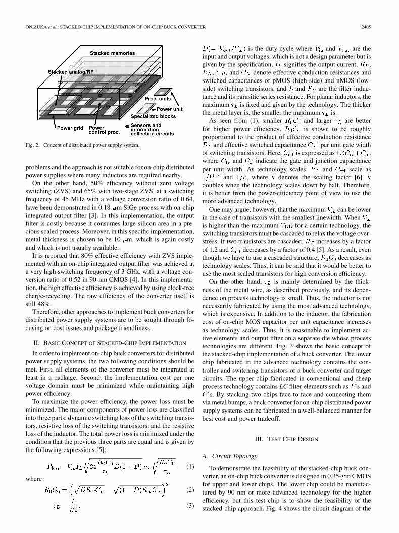
major integration technologies. They are often used to in-tegrate various types of circuit blocks from processors andmemories to analog circuits. Each block demonstrates a dif-ferent optimum supply voltage and the difference tendsto increase as the technology scales. For example, memoryand analog circuits tend to prefer higher voltage comparedwith logic blocks. Fig. 1 shows the trends for precisionanalog/RF, performance analog/RF, high-performance logic,and low-power logic with the design rule trends according tothe International Technology Roadmap for Semiconductors(ITRS) 2005 [1]. Multiple- implementation is thereforerequired in low-power and high-performance systems. More-over, supply voltage is sometimes tuned in time to achievelower power consumption, which is called dynamic voltagescaling. The supply of many different and dynamically scaledvoltages from outside the package gives rise to much overheadin area. The power line integrity, including IR drop and noise,becomes an issue as well. The distributed on-chip power supplycircuits are useful for solving these problems. The concept ofthe distributed power supply is shown in Fig. 2. High voltage is
Manuscript received February 19, 2007; revised May 29, 2007.K. Onizuka, K. Inagaki, and M. Takamiya are with the Institute of Indus-
trial Science, University of Tokyo, Tokyo 153-8505, Japan (e-mail: [email protected]).
H. Kawaguchi is with the Department of Computer and Systems Engineering,Kobe University, Kobe 657-8501, Japan.
T. Sakurai is with the Center for Collaborative Research, University of Tokyo,Tokyo 153-8505, Japan.
Digital Object Identifier 10.1109/JSSC.2007.906204
Fig. 1. Supply voltage trend with design rule trend according to ITRS.
distributed by a main power grid and is then converted to thelower voltages at the vicinity of the target blocks by distributedon-chip voltage converters. This approach reduces cost andpower integrity issues.
For dc–dc converters, linear regulator, buck converters andswitched capacitor converter are well known circuits. A buckconverter requires large passive elements of inductance and ca-pacitance (LC) for an output filter but it shows a higher power ef-ficiency than a linear regulator. A switched-capacitor converteralso needs large capacitors and one more drawback is that theoutput voltage levels are limited by the ratios of prepared capac-itors. That is not very suitable for low-power dynamic voltagescaling systems.
In case of the buck converter, high switching frequency ispreferable for smaller L and C but the power efficiency is de-graded by the dynamic power dissipated by switching transis-tors at high frequency. Low quality factor (Q) of air-core andon-chip inductors also degrades the power efficiency. High in-ductance is good for high Q but is not easy to obtain on a chipbecause of the area limitation and, even if high magnetic per-meability material is introduced on a chip, high- property isusually lost at high frequency.
A couple of integrated buck converters have been reportedin recent years. Efficiency of 80%-87% was achieved at a highswitching frequency of 233 MHz for voltage conversion ra-tios of 0.75 and 0.79 with off-chip air-core inductors in 90-nmCMOS process [2]. The air-core and surface-mount inductorswhose quality factors are over 20 contribute to higher power ef-ficiency. However, the part cost, the assembly cost and area are
0018-9200/$25.00 © 2007 IEEE
ONIZUKA et al.: STACKED-CHIP IMPLEMENTATION OF ON-CHIP BUCK CONVERTER 2405
Fig. 2. Concept of distributed power supply system.
problems and the approach is not suitable for on-chip distributedpower supplies where many inductors are required nearby.
On the other hand, 50% efficiency without zero voltageswitching (ZVS) and 65% with two-stage ZVS, at a switchingfrequency of 45 MHz with a voltage conversion ratio of 0.64,have been demonstrated in 0.18- m SiGe process with on-chipintegrated output filter [3]. In this implementation, the outputfilter is costly because it consumes large silicon area in a pre-cious scaled process. Moreover, in this specific implementation,metal thickness is chosen to be 10 m, which is again costlyand which is not usually available.
It is reported that 80% effective efficiency with ZVS imple-mented with an on-chip integrated output filter was achieved ata very high switching frequency of 3 GHz, with a voltage con-version ratio of 0.52 in 90-nm CMOS [4]. In this implementa-tion, the high effective efficiency is achieved by using clock-treecharge-recycling. The raw efficiency of the converter itself isstill 48%.
Therefore, other approaches to implement buck converters fordistributed power supply systems are to be sought through fo-cusing on cost issues and package friendliness.
II. BASIC CONCEPT OF STACKED-CHIP IMPLEMENTATION
In order to implement on-chip buck converters for distributedpower supply systems, the two following conditions should bemet. First, all elements of the converter must be integrated atleast in a package. Second, the implementation cost per onevoltage domain must be minimized while maintaining highpower efficiency.
To maximize the power efficiency, the power loss must beminimized. The major components of power loss are classifiedinto three parts: dynamic switching loss of the switching transis-tors, resistive loss of the switching transistors, and the resistiveloss of the inductor. The total power loss is minimized under thecondition that the previous three parts are equal and is given bythe following expressions [5]:
(1)
where
(2)
(3)
is the duty cycle where and are theinput and output voltages, which is not a design parameter but isgiven by the specification, signifies the output current, ,
, , and denote effective conduction resistances andswitched capacitances of pMOS (high-side) and nMOS (low-side) switching transistors, and and are the filter induc-tance and its parasitic series resistance. For planar inductors, themaximum is fixed and given by the technology. The thickerthe metal layer is, the smaller the maximum is.
As seen from (1), smaller and larger are betterfor higher power efficiency. is shown to be roughlyproportional to the product of effective conduction resistance
and effective switched capacitance per unit gate widthof switching transistors. Here, is expressed as ,where and indicate the gate and junction capacitanceper unit width. As technology scales, and scale as
and , where denotes the scaling factor [6].doubles when the technology scales down by half. Therefore,it is better from the power-efficiency point of view to use themore advanced technology.
One may argue, however, that the maximum can be lowerin the case of transistors with the smallest linewidth. Whenis higher than the maximum for a certain technology, theswitching transistors must be cascaded to relax the voltage over-stress. If two transistors are cascaded, increases by a factorof 1.2 and decreases by a factor of 0.4 [5]. As a result, eventhough we have to use a cascaded structure, decreases astechnology scales. Thus, it can be said that it would be better touse the most scaled transistors for high conversion efficiency.
On the other hand, is mainly determined by the thick-ness of the metal wire, as described previously, and its depen-dence on process technology is small. Thus, the inductor is notnecessarily fabricated by using the most advanced technology,which is expensive. In addition to the inductor, the fabricationcost of on-chip MOS capacitor per unit capacitance increasesas technology scales. Thus, it is reasonable to implement ac-tive elements and output filter on a separate die whose processtechnologies are different. Fig. 3 shows the basic concept ofthe stacked-chip implementation of a buck converter. The lowerchip fabricated in the advanced technology contains the con-troller and switching transistors of a buck converter and targetcircuits. The upper chip fabricated in conventional and cheapprocess technology contains LC filter elements such as ’s and
’s. By stacking two chips face to face and connecting themvia metal bumps, a buck converter for on-chip distributed powersupply systems can be fabricated in a well-balanced manner forbest cost and power tradeoff.
III. TEST CHIP DESIGN
A. Circuit Topology
To demonstrate the feasibility of the stacked-chip buck con-verter, an on-chip buck converter is designed in 0.35- m CMOSfor upper and lower chips. The lower chip could be manufac-tured by 90 nm or more advanced technology for the higherefficiency, but this test chip is to show the feasibility of thestacked-chip approach. Fig. 4 shows the circuit diagram of the

2406 IEEE JOURNAL OF SOLID-STATE CIRCUITS, VOL. 42, NO. 11, NOVEMBER 2007
Fig. 3. Basic concept of stacked-chip implementation of on-chip buckconverter.
Fig. 4. Test circuit diagram of stacked-chip implementation of buck converter.
buck converter. Parameters are optimized for the power effi-ciency as described hereinbelow. Drivabilities of the taperedbuffers are set high enough and the inverter sizes are calculatedto minimize the on–on overlap time of switching transistors. Theouter diameter of the filter equals that of the filter inductor ,which is set at 2 2 mm by assuming that a 10 mm chipcan have 25 voltage domains. A 6.8 6.9 mm chip with sevenvoltage domains has already been presented [7]. degrades asthe outer diameter of the inductor shrinks, however, the powerefficiency can be kept high because decreases as tech-nology scales. The inductance is estimated by a simple formulafrom [8]. Narrow metal-to-metal spacing and a wide metal wireare preferable in this application. is a function of theratio, which can be calculated using the inductance formula andthe sheet resistance. The inductance and the parasitic resistanceare roughly proportional to for a fixed ratio, where
is the number of turns, considering that the space is negligiblynarrow compared with the line width. The normalized curvein Fig. 5 is therefore independent of . From the calculation re-sult, is decided to be about . Here, is decided as3 to maximize the power efficiency. As a result, the calculatedinductance of this work is 22 nH when the sheet resistance isabout 0.02 . The open space at the center of the inductor isfilled with a MOS capacitor for the output filter. Area efficiencyis more important than linearity for the filter capacitor, becausethe output voltage does not change dynamically in normal oper-ation. From that aspect, the MOS capacitor is more suitable thanany other types of on-chip capacitors like metal–insulator–metal
Fig. 5. � dependence on d =d for square inductor.
Fig. 6. Estimated power efficiency dependence on load current and switchingfrequency.
(MIM) capacitor or polysilicon capacitor. The obtained capaci-tance is about 1 nF. Under those conditions, the power efficiencydependence on the output current and the switching frequencyfor V and V is plotted in Fig. 6 by mod-ifying the duty cycle definition in [11]. is redefined in thisstudy as follows to take the voltage drop caused by the filter in-ductor into account, when it is simply set as in[11]; by doing so, the estimation accuracy of several values isimproved:
(4)
Here, denotes the load current which equals the dc part ofthe inductor current.
The output voltage ripple ratio is described as follows whenand denote switching frequency and output filter capaci-
tance, respectively:
(5)
It is impossible to choose a switching frequency under100 MHz in this case because the output voltage ripple goesup above 10% for the chosen values. The gate width of thehigh-side and low-side transistors are designed to be 1000and 500 m, respectively, under the load current condition of60 mA using the optimum gate-width formulas in [11].

ONIZUKA et al.: STACKED-CHIP IMPLEMENTATION OF ON-CHIP BUCK CONVERTER 2407
Fig. 7. Chip microphotograph of the output filter.
Fig. 8. Measurement setup of the test chip.
B. Simulation and Measurement Results
The test buck converter with the stacked-chip implementationwas fabricated and measured. Fig. 7 shows the chip micropho-tograph of the output filter on the upper chip. Figs. 8 and 9 showthe measurement setup and its cross-sectional diagram. The padsize and the effective bump diameter of this experimental setupare m and 150 m, respectively. Micro bumps withdiameter 30 m and whose resistance is as low as 14 m bumphave been realized in industry environments [14] and can beused instead for further smaller area. The output waveform inFig. 10 shows V at mA. The measuredvoltage ripple is smaller than 10%, which is comparable to theresult of the more expensive solution in [2]. Fig. 11 shows thesimulated and measured power efficiency with Vfor an output current range from 20 to 70 mA. The maximumefficiency of 62% is achieved for 70 mA output current. Themeasurement results compare well with the HSPICE simulationresults. The simulation considers all of the parasitic elements,including the inductor parasitic resistance of 2.5 and the in-ductor input-to-ground capacitance of 25 pF.
Fig. 9. Cross-sectional diagram of the measurement setup.
Fig. 10. Output voltage waveform for V = 1:86 V and I = 60 mA.
Fig. 11. Simulated and measured power efficiency for V = 2:3 V and f =
200 MHz.
IV. IMPLEMENTING FILTER INDUCTOR ON GLASS
EPOXY INTERPOSER
In order to further increase the efficiency, it is effective to useinductors whose is higher than that of the previous induc-tors. A thin-film inductor surrounded by magnetic core materialas proposed in [15] can be a solution but is expensive. Imple-menting the inductor on a glass epoxy interposer as shown inFig. 12 is an effective yet inexpensive solution. The thickness ofthe metal wire on an interposer is generally thicker than 10 m,and the inductor on the interposer shows a much lower resis-tance than that on a silicon chip, where the metal thickness isusually less than 1 m. A capacitor on the upper chip made witha conventional technology is connected to the lower chip manu-factured by an advanced technology like 90 nm CMOS, throughthe through-hole vias in the interposer. By this implementation,

2408 IEEE JOURNAL OF SOLID-STATE CIRCUITS, VOL. 42, NO. 11, NOVEMBER 2007
Fig. 12. Another stacked-chip implementation to gain high � .
Fig. 13. Manufactured inductor array on glass epoxy interposer.
high efficiency and low cost are achieved at the same time. Themaximum power efficiency is derived as follows from (1):
(6)
Here, indicates the output power. is a function ofand and can be a constant when the process technology
and are fixed. Therefore, simply higher directly results inhigher power efficiency.
The structure shown in Fig. 12 is assembled using a newlyintroduced interposer and the same lower and upper chips pre-sented in Section III. In this implementation, only a capacitoris used on the upper chip. Fig. 13 shows an inductor arrayon generic Flame Resistant 4 (FR-4) glass epoxy interposerwith two metal layers. The circled inductor in the array, whichachieved the minimum metal spacing in the trial manufac-ture, is used for the measurement. The metal thickness onthe interposer is 30 m, the substrate thickness is 100 m,and the dia-meter of the through-hole via is 100 m. Thisimplementation increases by 30 times compared with thecase of an on-chip inductor. The outer diameter of the inductor
Fig. 14. Cross-sectional diagram of the measurement setup.
Fig. 15. Measured efficiency comparison between two types ofimplementations.
is increased by 10% to achieve the same value of on-chip filterinductance because the minimum spacing of metal lands onglass epoxy is larger than that of on-chip interconnects. Thepermittivity of the glass epoxy is generally more than four timeshigher than SiO , however, the parasitic capacitance betweenboth sides of the interposer can be negligible. This is becausethe substrate thickness is sufficiently large compared with theline width. Fig. 14 shows the cross section of the stacked chips.Fig. 15 shows the comparison of measured power efficiencybetween two types of implementations of “two chips” and “twochips + interposer” for V and V. Thepower efficiency with the glass epoxy inductor is improved by5%–14% depending on the output current compared with theon-chip implementation. The maximum power efficiency of71.3% is achieved at an output current of 60 mA. The possiblereason that the efficiency does not improve the most at 60 mAis that the switching transistors are not changed optimallyaccording to the characteristic of the newly implementedinductor.
V. CONCLUSION
An on-chip buck converter with stacked-chip implementationthat is suitable for low-cost low-power distributed power supplysystems has been designed and fabricated for the first time. Theswitching frequency is optimized and chosen to be 200 MHz.A power efficiency of 62% is measured for an output current of70 mA, which verifies the feasibility of this approach. By uti-lizing a glass epoxy interposer for a filter inductor, it is shown byexperiment that the power efficiency can be increased to 71.3%.

ONIZUKA et al.: STACKED-CHIP IMPLEMENTATION OF ON-CHIP BUCK CONVERTER 2409
ACKNOWLEDGMENT
The authors would like to thank K. Osada, Hitachi, Ltd., andS. Borkar, R. Krishnamurthy, S. Hsu, T. Karnik, and G. Schrom,Intel laboratories, for valuable discussions. The chip fabricationwas supported by VLSI Design and Education Center (VDEC),University of Tokyo, with collaboration by Synopsys, RohmCorporation, and Toppan Printing Corporation.
REFERENCES
[1] The International Technology Roadmap for Semiconductors2005 [Online]. Available: http://www.itrs.net/Common/2005ITRS/Home2005.htm
[2] P. Hazucha, G. Schrom, J.-H. Hahn, B. Bloechel, P. Hack, G. Dermer,S. Narendra, D. Gardner, T. Karnik, V. De, and S. Borker, “A 233-MHz, 80%–87% efficient four-phase DC-DC converter utilizing air-core inductors on package,” IEEE J. Solid-State Circuits, vol. 40, no.4, pp. 838–845, Apr. 2005.
[3] S. Abedinpour, B. Bakkaloglu, and S. Kiaei, “A multi-stage interleavedsynchronous buck converter with integrated output filter in a 0.18 �mSiGe process,” in IEEE ISSCC Dig. Tech, Papers, 2006, pp. 356–357.
[4] M. Alimadadi, S. Sheikhaei, G. Lemieux, S. Mirabbasi, and P. Palmer,“A 3 GHz switching DC-DC converter using clock-tree charge-recy-cling in 90 nm CMOS with integrated output filter,” in IEEE ISSCCDig. Tech. Papers, 2007, pp. 532–5533.
[5] G. Schrom, P. Hazucha, F. Paillet, D. S. Gardner, S. T. Moon, and T.Karnik, “Optimal design of monolithic integrated DC-DC converters,”in Proc. IEEE Int. Conf. IC Design Technology, 2006, pp. 65–67.
[6] T. Sakurai and R. Newton, “Alpha-power law MOSFET model andits applications to CMOS inverter delay and other formulas,” IEEE J.Solid-State Circuits, vol. 25, no. 2, pp. 584–594, Feb. 1990.
[7] G. Uvieghara, M.-C. Kuo, J. Arceo, J. Cheung, J. Lee, X. Niu,R. Sankuratri, M. Severson, O. Arias, Y. Chang, S. King, K.-C.Lai, Y. Tian, S. Varadarajan, J. Wang, K. Yen, L. Yuan, N. Chen,D. Hsu, D. Lisk, S. Khan, A. Fahim, C.-L. Wang, J. Dejaco, Z.Mansour, and M. Sani, “A highly-integrated 3G CDMA2000 1Xcellular baseband chip with GSM/AMPS/GPS/Bluetooth/Multimediacapabilities and ZIF RF support,” in IEEE ISSCC Dig. Tech. Papers,2004, pp. 422–536.
[8] S. S. Mohan, M. del Mar Hershenson, S. P. Boyd, and T. H. Lee,“Simple accurate expressions for planar spriral inductors,” IEEE J.Solid-State Circuits, vol. 34, no. 10, pp. 1419–1424, Oct. 1999.
[9] V. Kursun, S. G. Narendra, V. K. De, and E. G. Friedman, “Efficiencyanalysis of a high frequency buck converter for on-chip integration witha dual-V microprocessor,” in Proc. Eur. Solid-State Circuits Conf.,Sep. 2002, pp. 743–746.
[10] V. Kursun, S. G. Narendra, V. K. De, and E. G. Friedman, “Mono-lithic DC-DC converter analysis and MOSFET gate voltage optimiza-tion,” in Proc. 4th Int. Symp. Quality Electronic Design, Mar. 2003, pp.279–284.
[11] V. Kursun, S. G. Narendra, V. K. De, and E. G. Friedman, “Analysisof buck converters for on-chip integration with a dual supply voltagemicroprocessor,” IEEE Trans. Very Large Scale Integr. (VLSI) Syst.,vol. 11, no. 3, pp. 514–522, Jun. 2003.
[12] V. Kursun, S. G. Narendra, V. K. De, and E. G. Friedman, “Low-voltage-swing monolithic dc-dc conversion,” IEEE Trans. CircuitsSyst. II, Exp. Briefs, vol. 51, no. 5, pp. 241–248, May 2004.
[13] G. Schrom, P. Hazucha, J. Hahn, D. S. Gardner, B. A. Bloechel, G.Dermer, S. G. Narendra, T. Karnik, and V. De, “A 480-MHz, multi-phase interleaved buck DC-DC converter with hysteretic control,” inProc. 35th Annu. IEEE Power Electronics Specialists Conf., Jun. 2004,pp. 4702–4707.
[14] T. Ezaki, K. Kondo, H. Ozaki, N. Sasaki, H. Yonernura, M. Kitano,S. Tanaka, and T. Hirayarna, “A 160 Gb/s interface design configura-tion for multichip LSI,” in IEEE ISSCC Dig. Tech. Papers, 2004, pp.140–141.
[15] G. Schrom, P. Hazucha, J.-H. Hahn, V. Kursun, D. Gardner, S.Narendra, T. Karnik, and V. De, “Feasibility of monolithic and3D-stacked DC-DC converters for mircoprocessors in 90 nm tech-nology generation,” in Proc. ISLPED, 2004, pp. 263–268.
Kohei Onizuka (S’03) received the B.S. degree ininformation and communication engineering and theM.S. degree in electronic engineering from the Uni-versity of Tokyo, Tokyo, Japan, in 2003 and 2005, re-spectively. He is currently working toward the Ph.D.degree at the University of Tokyo.
His research interests include high-speedV -hopping, on-chip dc–dc converters, andchip-to-chip wireless power transmission for SiPapplications.
Kenichi Inagaki (M’00) received the B.S. and M.S.degrees in earth and planetary sciences from theTokyo Institute of Technology, Tokyo, Japan, in1997 and 1999, respectively.
Since 1999, he has been a Technical Associate withthe University of Tokyo, Tokyo. His current work isin the area of analysis of signal and power integrityon VLSI circuits.
Hiroshi Kawaguchi (M’98) received the B.E. andM.E. degrees in electronic engineering from ChibaUniversity, Chiba, Japan, in 1991 and 1993, respec-tively, and the Ph.D. degree in engineering from theUniversity of Tokyo, Tokyo, Japan, in 2006.
He joined Konami Corporation, Kobe, Japan, in1993, where he developed arcade entertainment sys-tems. He moved to the Institute of Industrial Science,University of Tokyo, as a Technical Associate in 1996and was appointed a Research Associate in 2003. In2005, he moved to the Department of Computer and
Systems Engineering, Kobe University, Kobe, Japan, as a Research Associate.Since 2007, he has been an Associate Professor with the Department of Com-puter Science and Systems Engineering, Kobe University. He is also a Collab-orative Researcher with the Institute of Industrial Science, University of Tokyo.His current research interests include low-power VLSI design, hardware designfor wireless sensor network, and recognition processor.
Dr. Kawaguchi is a member of Association of Computing Machinery. He wasa recipient of the IEEE ISSCC 2004 Takuo Sugano Outstanding Paper Awardand the IEEE Kansai Section 2006 Gold Award. He has served as a ProgramCommittee Member for the IEEE Symposium on Low-Power and High-SpeedChips (COOL Chips) and as a Guest Associate Editor of IEICE Transactionson Fundamentals of Electronics, Communications and Computer Sciences.
Makoto Takamiya (S’98-M’00) received the B.S.,M.S., and Ph.D. degrees in electronic engineeringfrom the University of Tokyo, Tokyo, in 1995, 1997,and 2000, respectively.
In 2000, he joined NEC Corporation, Japan, wherehe was engaged in the circuit design of high-peeddigital LSIs and developed the field of on-chip mea-surement macros to solve the power in-tegrity issues.In 2005, he joined University of Tokyo, where he isan Associate Professor of VLSI Design and Educa-tion Center. His research interests include power and
signal integrity issues, low-power RF integrated circuits, and large-rea elec-tronics with organic transistors.

2410 IEEE JOURNAL OF SOLID-STATE CIRCUITS, VOL. 42, NO. 11, NOVEMBER 2007
Takayasu Sakurai (S’77–M’78–SM’01–F’03)received the Ph.D. degree in electrical engineeringfrom the University of Tokyo, Tokyo, Japan, in 1981.
In 1981, he joined Toshiba Corporation, where hedesigned CMOS DRAM, SRAM, RISC processors,DSPs, and SoC solutions. He has worked extensivelyon interconnect delay and capacitance modelingknown as the Sakurai model and alpha power-lawMOS model. From 1988 through 1990, he was a Vis-iting Researcher with the University of California,Berkeley, where he conducted research in the field of
VLSI CAD. Since 1996, he has been a Professor wit the University of Tokyo,working on low-power high-speed VLSI, memory design, interconnects,
ubiquitous electronics, organic ICs and large-area electronics. He has publishedmore than 350 technical publications, including 70 invited publications andseveral books, and has filed more than 100 patents. He served as a conferencechair for the Symposium on VLSI Circuits and ICICDT, a vice chair forASPDAC, a TPC chair for the first A-SSCC, and VLSI Symposium, and aprogram committee member for ISSCC, CICC, DAC, ESSCIRC, ICCAD,FPGA Workshop, ISLPED, TAU, and other international conferences. He is aplenary speaker for the 2003 ISSCC.
Dr. Sakurai is a STARC Fellow, an elected AdCom member for the IEEESolid-State Circuits Society, and an IEEE Circuits and System SocietyDistinguished Lecturer. He was a recipient of te 2005 IEEE ICICDT Award, te2005 IEEE ISSCC Takuo Sugano Award, and te 2005 P&I Patent of the YearAward.