2019 NEPP ETW: 2D, 2.1D, 2.5D, and 3D Package Studies in NEPP · 3D Package Studies in NEPP •...
15
2D, 2.1D, 2.5D, and 3D Package Studies in NEPP Eric J Suh Joseph Riendeau Jet Propulsion Laboratory, California Institute of Technology NASA Electronic Parts and Packaging Program (NEPP) 2019 Annual NEPP Electronic Technology Workshop (ETW) June 18th, 2019 1
Transcript of 2019 NEPP ETW: 2D, 2.1D, 2.5D, and 3D Package Studies in NEPP · 3D Package Studies in NEPP •...
2D, 2.1D, 2.5D, and 3D Package Studies in NEPP
Eric J Suh
Joseph Riendeau
Jet Propulsion Laboratory, California Institute of Technology
NASA Electronic Parts and Packaging Program (NEPP)
2019 Annual NEPP Electronic Technology Workshop (ETW)
June 18th, 2019
1

2D, 2.1D, 2.5D and 3D Packages
2.5D
2D/2.1D SiP
3D
Ceramic Flip Chip (Class-Y / V)
Present
Space Parts
Past
NEPPOrganic Flip Chip
2D
Present
NEPP
Future
NEPP
FY16
FY17~18
FY18~19

Past NEPP Studies on 2D Packages
• Ceramic flip chip packages : Class V and Y flip chip packages. – ex) RTG4 and Virtex-5
• NEPP systematically supported studies on Class-Y packages.
3
FY Title
Thermal management using
heat transfer device
2014 Thermal Interface Materials Selection and
Application Guidelines
Heat spread thermal
interface material
2012 Physics of Failure Analysis of Xilinx Flip Chip CCGA
Packages
Underfill material 2011 Underfill Materials for Reliable Flip chip Packaging
2012 Physics of Failure Analysis of Xilinx Flip Chip CCGA
Packages
Ceramic flip chip solder
joints and underfill
2012/
2013
Aeroflex Technology as Class-Y Demonstrator
1752 CCGA Columns 2015 Virtex 5 CN Daisy Chain Evaluation
Heat

Organic Flip Chip Package Studies in NEPP
4
• Organic substrate can offer smaller feature size than ceramic substrate.
• NEPP partnered with Cobham and evaluated organic flip chip for space.
• Based on NEPP / Cobham study results, JEDEC task group was formed to bring organic flip chip technology into MIL-PRF-38535.
HTCC Organic
Bump Pad Diameter (µm) ~150 >60
Bump Pad Pitch (µm) ~250 >120
Trace Line Width (µm) 100~125 9~15
Trace Line Spacing (µm) 100~125 12~15
Via Diameter (µm) 125~200 50~65 (12mil for core)
Via Pitch (µm) 250~640 100~125 (40mil for core)
Dielectric Const. 8.5~10 3.2~4.8
Dielectric Loss Angle 0.0005~0.007 0.019~0.248
Trace Sheet Resistance (mΩ/sq) 8~17 3
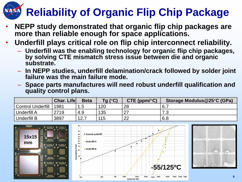
Reliability of Organic Flip Chip Package
• NEPP study demonstrated that organic flip chip packages are more than reliable enough for space applications.
• Underfill plays critical role on flip chip interconnect reliability.– Underfill was the enabling technology for organic flip chip packages,
by solving CTE mismatch stress issue between die and organic substrate.
– In NEPP studies, underfill delamination/crack followed by solder joint failure was the main failure mode.
– Space parts manufactures will need robust underfill qualification and quality control plans.
5
Char. Life Beta Tg (°C) CTE (ppm/°C) Storage Modulus@25°C (GPa)
Control Underfill 1981 1.5 120 28 6.7
Underfill A 2719 4.9 135 27 7.3
Underfill B 3897 12.7 115 22 6.8
15x15
mm
-55/125ºC
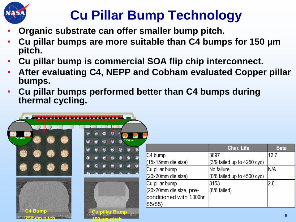
• Organic substrate can offer smaller bump pitch.
• Cu pillar bumps are more suitable than C4 bumps for 150 µm pitch.
• Cu pillar bump is commercial SOA flip chip interconnect.
• After evaluating C4, NEPP and Cobham evaluated Copper pillar bumps.
• Cu pillar bumps performed better than C4 bumps during thermal cycling.
Cu Pillar Bump Technology
6C4 Bump
250 µm pitch
Cu pillar Bump
150 µm pitch
Char. Life Beta
C4 bump
(15x15mm die size)
3897
(3/9 failed up to 4250 cyc)
12.7
Cu pillar bump
(20x20mm die size)
No failure.
(0/6 failed up to 4500 cyc)
N/A
Cu pillar bump
(20x20mm die size, pre-
conditioned with 1000hr
85/85)
3153
(6/6 failed)
2.8
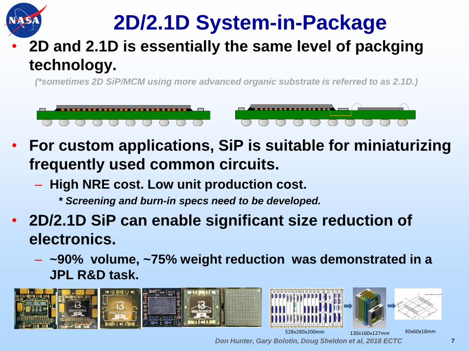
2D/2.1D System-in-Package• 2D and 2.1D is essentially the same level of packging
technology.(*sometimes 2D SiP/MCM using more advanced organic substrate is referred to as 2.1D.)
• For custom applications, SiP is suitable for miniaturizing
frequently used common circuits.
– High NRE cost. Low unit production cost.
* Screening and burn-in specs need to be developed.
• 2D/2.1D SiP can enable significant size reduction of
electronics.
– ~90% volume, ~75% weight reduction was demonstrated in a
JPL R&D task.
7Don Hunter, Gary Bolotin, Doug Sheldon et al, 2018 ECTC
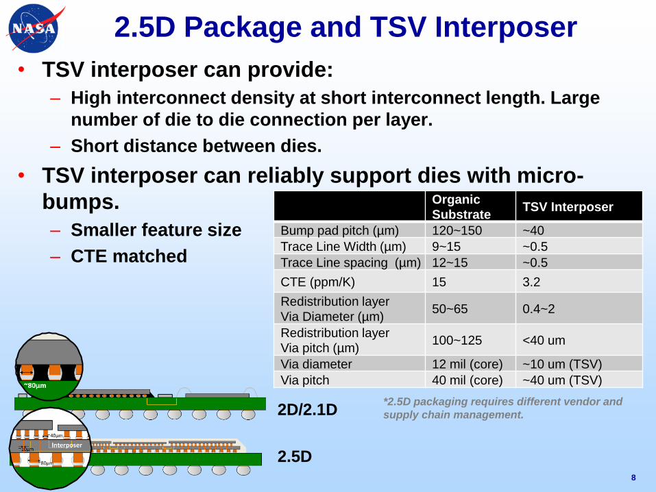
• TSV interposer can provide:
– High interconnect density at short interconnect length. Large
number of die to die connection per layer.
– Short distance between dies.
• TSV interposer can reliably support dies with micro-
bumps.
– Smaller feature size
– CTE matched
2.5D Package and TSV Interposer
8
2.5D
2D/2.1D
Organic
SubstrateTSV Interposer
Bump pad pitch (µm) 120~150 ~40
Trace Line Width (µm) 9~15 ~0.5
Trace Line spacing (µm) 12~15 ~0.5
CTE (ppm/K) 15 3.2
Redistribution layer
Via Diameter (µm)50~65 0.4~2
Redistribution layer
Via pitch (µm)100~125 <40 um
Via diameter 12 mil (core) ~10 um (TSV)
Via pitch 40 mil (core) ~40 um (TSV)
*2.5D packaging requires different vendor and
supply chain management.

3D Package Studies in NEPP
• NEPP study on 3D COTS DDR4 SDRAM.
– SOA COTS 3D packaging.
– High-quality production process by a major manufacturer.
– Easily available.
9
Samsung TSV DDR4
TSV&
Microbumps
Flip Chip bump
Diameter (µm) Height (µm)
TSV 5~6 50~60
Microbump ~40 ~20
Flip Chip Bump ~65 ~35
4 stacked die
Substrate
(NCP or NCF)
Underfill
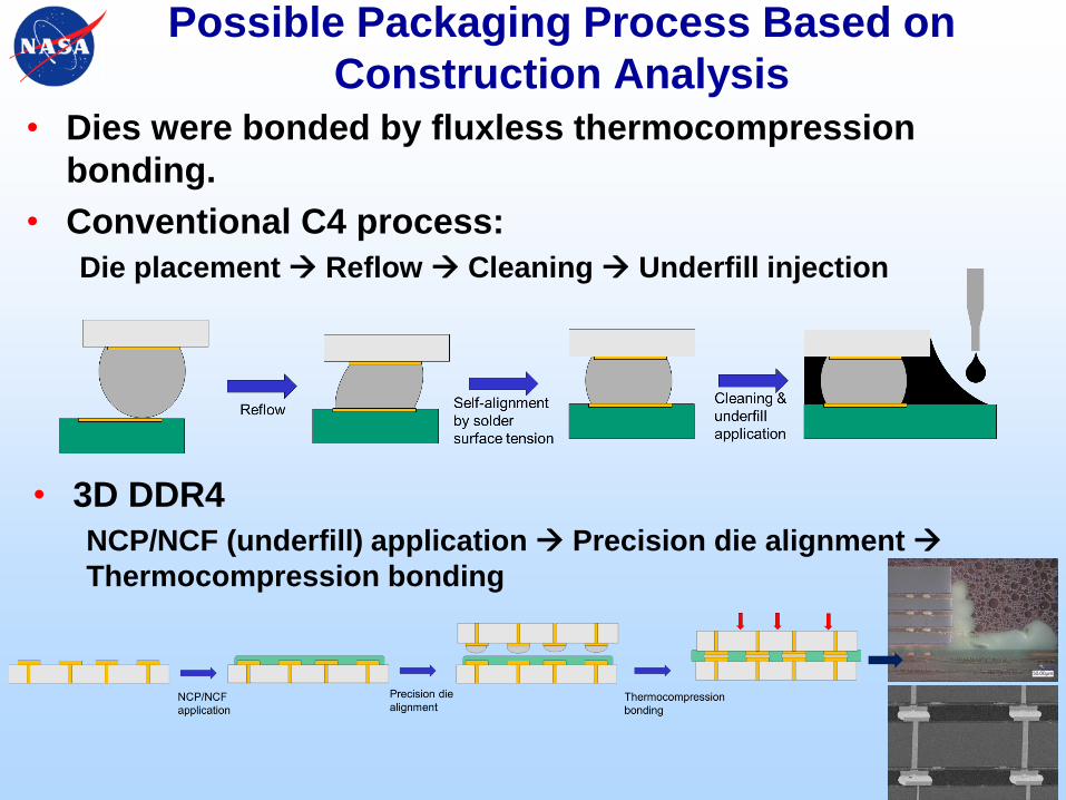
Possible Packaging Process Based on
Construction Analysis
• Dies were bonded by fluxless thermocompression
bonding.
• Conventional C4 process:
Die placement Reflow Cleaning Underfill injection
• 3D DDR4
NCP/NCF (underfill) application Precision die alignment
Thermocompression bonding
10

DDR4 Temp Cycling Test
• Electrical testing was done on DIMM up to 1250 cycles
from -55 to 125ºC.
– Typical functional failure took place between 250 to 750 cycles.
• Qualitative study was done instead of quantitative study.
– Dominant failure mode was investigated, instead of
characterizing the thermal cycling life.
• Groups of 16 devices were subjected to varying number
of cycles, from -55 to 125ºC.
• Devices were both non-destructively and destructively
analyzed to look for physical damage.
11
# Cycles
-55/1250 500 1000 1500 2000 2500 3000 3500 4000
SN 1, 11 2,12 3,13 4,14 5,15 6,16 7,17 8,18 9,19
* 8 devices per SN. (16 devices per condition.)

Nondestructive Analysis
• NDA was done using a Zeiss x-ray microscope.
– Unlike microCT, x-ray microscope optically magnifies x-ray image
with lenses.
• A sample subjected to 4000 cycles were inspected.
• A flip chip bump between the bottom die and the
substrate was suspected for crack.
12
SEM Image for reference
X-ray microscope image of a
cracked bump
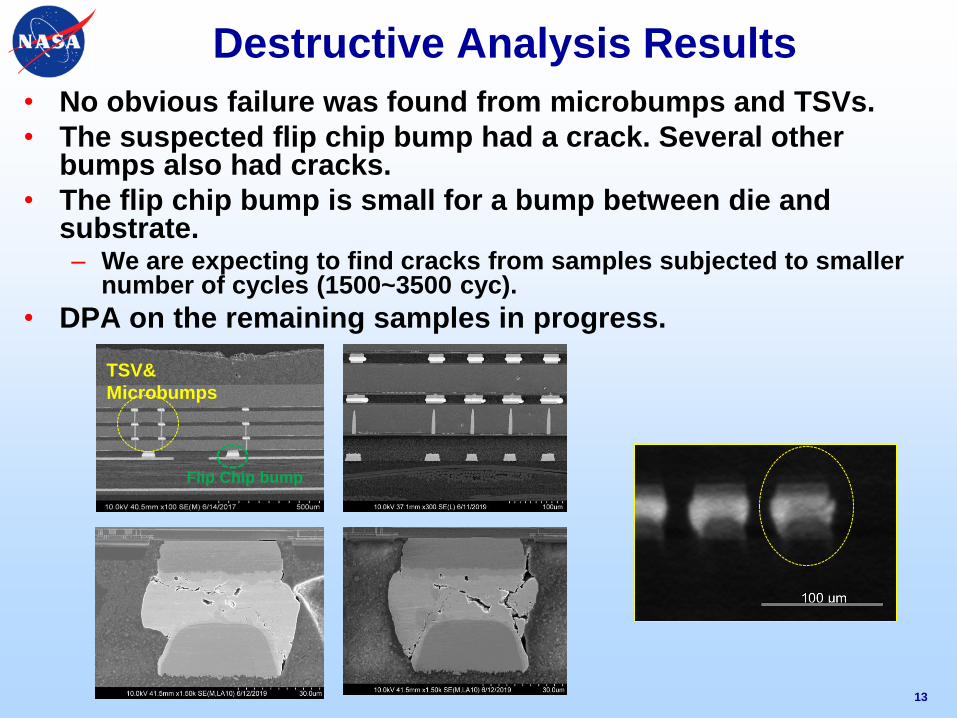
Destructive Analysis Results
• No obvious failure was found from microbumps and TSVs.
• The suspected flip chip bump had a crack. Several other bumps also had cracks.
• The flip chip bump is small for a bump between die and substrate. – We are expecting to find cracks from samples subjected to smaller
number of cycles (1500~3500 cyc).
• DPA on the remaining samples in progress.
13
TSV&
Microbumps
Flip Chip bump

Future NEPP Studies on 2.5D and 3D
Packages
• Next generation interposers are competing with TSV.
– Cost reduction is the main technology driver.
• 2 major candidate technologies
– Organic interposer : Initiated a joint task with Cobham.
– Glass interposer : Currently discussing possibility of joint task
with Georgia Tech.
• Additional advantages of organic and glass interposers
– Interposers with BGAs can be directly assembled on PCB.
• Organic interposer CTE : 10~11ppm/K
• Glass interposer CTE: 3~10 ppm/K (CTE can be tailored)
14
Substrate
Summary
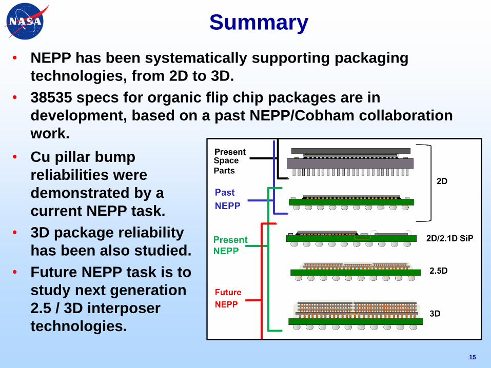
• NEPP has been systematically supporting packaging
technologies, from 2D to 3D.
• 38535 specs for organic flip chip packages are in
development, based on a past NEPP/Cobham collaboration
work.
15
• Cu pillar bump
reliabilities were
demonstrated by a
current NEPP task.
• 3D package reliability
has been also studied.
• Future NEPP task is to
study next generation
2.5 / 3D interposer
technologies.
Space
Parts