NEPP Roadmaps, COTS, and Small Missions · PDF file6/14/2016 · NEPP Roadmaps,...
22
NEPP Roadmaps, COTS, and Small Missions Kenneth A. LaBel Michael J. Sampson [email protected] [email protected] 301-286-9936 301-614-6233 Co- Managers, NEPP Program NASA/GSFC http://nepp.nasa.gov Open Access 1 Presented by Kenneth A. LaBel at the 2016 NEPP Electronics Technology Workshop (ETW), Goddard Space Flight Center, Greenbelt, Maryland, June 13–16, 2016. Acknowledgment: This work was sponsored by: NASA Office of Safety & Mission Assurance Sundown at SCRIPPS Proton Therapy Center, Ken LaBel
Transcript of NEPP Roadmaps, COTS, and Small Missions · PDF file6/14/2016 · NEPP Roadmaps,...

NEPP Roadmaps, COTS, and Small Missions
Kenneth A. LaBel Michael J. [email protected] [email protected]
301-286-9936 301-614-6233Co- Managers, NEPP Program
NASA/GSFChttp://nepp.nasa.gov
Open Access1Presented by Kenneth A. LaBel at the 2016 NEPP Electronics Technology Workshop (ETW), Goddard Space Flight Center, Greenbelt, Maryland, June 13–16, 2016.
Acknowledgment:This work was sponsored by:NASA Office of Safety & Mission Assurance
Sundown at SCRIPPS Proton Therapy Center,Ken LaBel
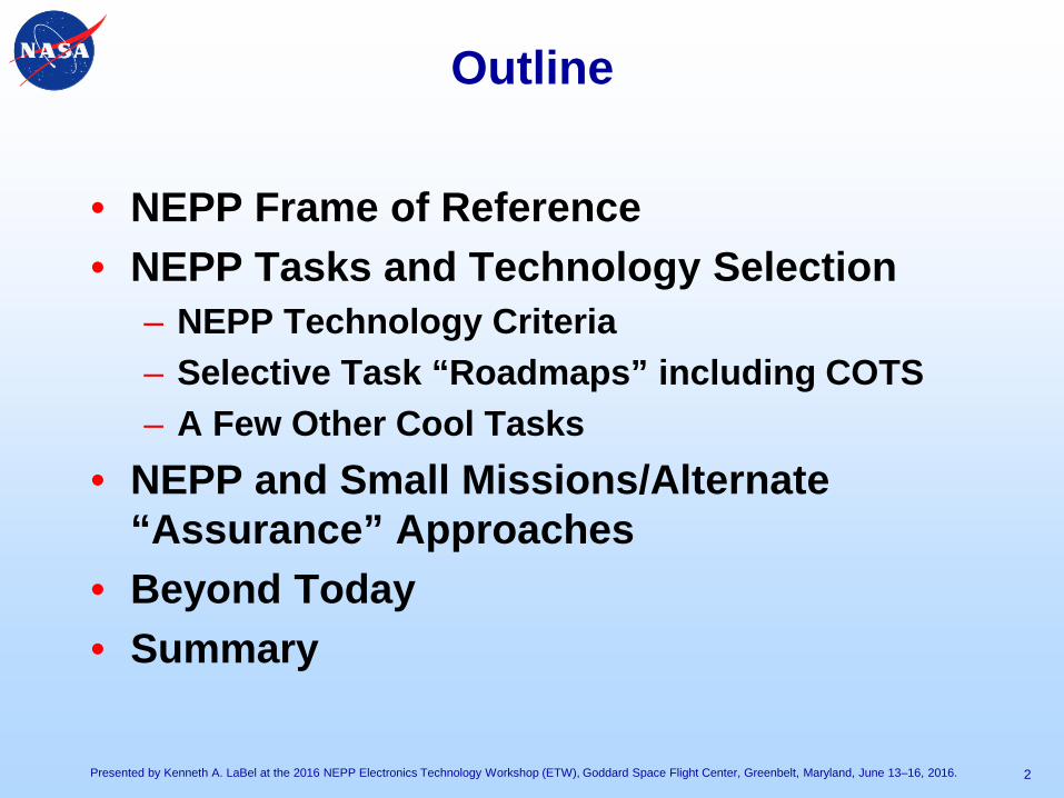
Outline
• NEPP Frame of Reference• NEPP Tasks and Technology Selection
– NEPP Technology Criteria– Selective Task “Roadmaps” including COTS– A Few Other Cool Tasks
• NEPP and Small Missions/Alternate “Assurance” Approaches
• Beyond Today• Summary
2Presented by Kenneth A. LaBel at the 2016 NEPP Electronics Technology Workshop (ETW), Goddard Space Flight Center, Greenbelt, Maryland, June 13–16, 2016.
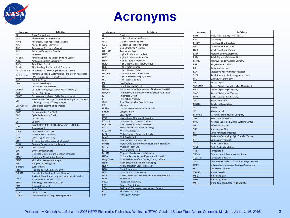
Acronyms
3Presented by Kenneth A. LaBel at the 2016 NEPP Electronics Technology Workshop (ETW), Goddard Space Flight Center, Greenbelt, Maryland, June 13–16, 2016.
Acronym Definition 3D Three Dimensional ACE Absolute Contacting EncoderADAS Advanced Driver Assistance SystemsADC Analog to Digital Converter AEC Automotive Electronics CouncilAES Advanced Encryption StandardAF Air ForceAF SMC Air Force Space and Missile Systems CenterAFRL Air Force Research LaboratoryAMS Agile Mixed SignalARM ARM Holdings Public Limited CompanyAvalanche STT Avalanche Technology Spin Transfer Torque
BAE Systems Marconi Electronic Systems (MES) and British Aerospace (BAe) merged to form BAE Systems
BGA Ball Grid ArrayBOK Body of Knowledge CAN Controller Area NetworkCBRAM Conductive Bridging Random Access MemoryCGA Column Grid ArrayCMOS Complementary Metal Oxide Semiconductor
CN Xilinx ceramic flip-chip (CF and CN) packages are ceramic column grid array (CCGA) packages
CN/Kyocera CN Package assembled at KyoceraCorp. CorporationCOTS Commercial Off The Shelf CRC Cyclic Redundancy CheckCU Control UnitCu Cu alloy
DDR Double Data Rate (DDR3 = Generation 3; DDR4 = Generation 4)
DMA Direct Memory AccessDoD Department of DefenseDSP Digital Signal ProcessingdSPI Dynamic Signal Processing InstrumentDTRA Defense Threat Reduction AgencyDual Ch. Dual ChannelECC Error-Correcting CodeEEE Electrical, Electronic, and Electromechanical EMAC Equipment Monitor And ControlEMIB Multi-die Interconnect BridgeESA European Space AgencyeTimers Event TimersFCCU Fluidized Catalytic Cracking UnitFeRAM Ferroelectric Random Access Memory
FinFET Fin Field Effect Transistor (the conducting channel is wrapped by a thin silicon "fin")
FPGA Field Programmable Gate Array FPU Floating Point UnitFY Fiscal Year GaN Gallium Nitride GAN GIT Panasonic GaN GIT Eng Prototype Sample
Acronym Definition Gb GigabyteGIC Global Industry ClassificationGPU Graphics Processing UnitGSFC Goddard Space Flight Center GSN Goal Structured NotationGTH/GTY Transceiver TypeHALT Highly Accelerated Life Test HAST Highly Accelerated Stress TestHBM High Bandwidth MemoryHDIO High Density Digital Input/OutputHDR High-Dynamic-RangeHMC Hybrid Memory CubeHP Labs Hewlett-Packard LaboratoriesHPIO High Performance Input/OutputHPS High Pressure SodiumI/O input/outputI2C Inter-Integrated Circuiti2MOS Microsemi second generation of Rad-Hard MOSFETIBM/GF International Business Machines/Global FoundariesIC Integrated CircuitIP Intellectual PropertyJPEG Joint Photographic Experts GroupKB KilobyteLinFlex Local Interconnect Network FlexibleL-mem Long-MemoryLP Low PowerLVDS Low-Voltage Differential SignalingLW HPS Lightwatt High Pressure SodiumM/L BIST Memory/Logic Built-In Self-TestMBSE Model-Based Systems EngineeringMil/Aero Military/AerospaceMIPI Mobile Industry Processor InterfaceMMC MultiMediaCardMMU Memory Management UnitMOSFETs Metal-Oxide-Semiconductor Field-Effect TransistorsMPFE Multiport Front-EndMPU Microprocessor UnitMRAM Magnetic Random Access MemoryNASA National Aeronautics and Space Administration Navy Crane Naval Surface Warfare Center, Crane, IndianaNEPP NASA Electronic Parts and Packaging NGSP Next Generation Space ProcessorNOR Not OR logic gateNRL Naval Research LaboratoryNRO United States Navy National Reconnaissance OfficeOCM on-chip RAMPBGA Plastic Ball Grid Array PCB Printed Circuit BoardPCIe Peripheral Component Interconnect ExpressPLL Phase Locked LoopPoP Package on Package
Acronym Definition PPAP Production Part Approval ProcessProc. ProcessingPS-GTR High Speed Bus InterfaceQFN Quad Flat Pack No LeadQSPI Serial Quad Input/OutputR&D Research and DevelopmentR&M Reliability and MaintainabilityReRAM Resistive Random Access MemoryRGB Red, Green, and BlueRH Radiation HardenedSAR Successive-Approximation-RegisterSATA Serial Advanced Technology AttachmentSCU Secondary Control UnitSD Secure DigitalSD/eMMC Secure Digital embedded MultiMediaCardSD-HC Secure Digital High CapacitySDIO Secure Digital Input/OutputSDM Spatial-Division-MultiplexingSEE Single Event EffectSERDES Serializer/DeserializerSi Silicon SiC Silicon Carbide SK Hynix SK Hynix Semiconductor CompanySLU Saint Louis UniversitySMC Air Force Space and Missile Systems CenterSOA Safe Operating AreaSOC Systems on a Chip SPI Serial Peripheral InterfaceSTT Avalanche Technology Spin Transfer TorqueSTT Spin Transfer Torque TBD To Be DeterminedTCM Trellis Code ModulationTemp TemperatureTHD+N Total Harmonic Distortion Plus NoiseT-Sensor Temperature-SensorTSMC Taiwan Semiconductor Manufacturing CompanyUART Universal Asynchronous Receiver/TransmitterUSB Universal Serial BusVNAND Vertical NAND WBG Wide Band GapWDT Watchdog TimerWSTS World Semiconductor Trade Statistics

NEPP - Frame of Reference• EEE (electrical, electronic, and
electromechanical) parts are:– All the things that are on printed circuit
boards (PCB) inside of electronics boxes.• This includes:
– Integrated Circuits (ICs or chips) like processors and memories as well as passives such as capacitors and resistors,
– Hybrid devices or multi-chip modules: Small packages that house multiple chips internally that are placed on the PCB, and,
– Connectors and wires used to send electrical or power signals between boards, boxes, or systems.
• This does not include:– The PCB - NASA Workmanship Program
responsibility.4
PCB from Mars Rover
Presented by Kenneth A. LaBel at the 2016 NEPP Electronics Technology Workshop (ETW), Goddard Space Flight Center, Greenbelt, Maryland, June 13–16, 2016.
Image courtesy NASA
Image courtesy NASA
Image courtesy BAE Systems

Motivational Factors
5
Military and Aerospace share is estimated at ~$3.1B in 2015.Aerospace is a small percentage of this amount.
In 1975, Military and Aerospace market share was ~$50%!Conclusion: Mil/Aero community has to leverage.
There’s no business model to go it alone!Presented by Kenneth A. LaBel at the 2016 NEPP Electronics Technology Workshop (ETW), Goddard Space Flight Center, Greenbelt, Maryland, June 13–16, 2016.
Technology Selection Criteriafor NEPP Investigations
• The technologies should satisfy all or most of the following criteria:– Wide applicability,– Product level or in productization, and,– No distinction: COTS to high-reliability aerospace.
• In general, we avoid:– Laboratory technologies, e.g., <TRL3,– Limited application devices with certain exceptions
(critical application or NASA center specialization).• Note: Partnering arrangements with other
organizations preferred.– Industry examples: Microsemi, Xilinx, Altera (Intel), TI– Other U.S. Government: AF SMC, AFRL, DTRA, Navy Crane,
NRO, NRL, etc…
Presented by Kenneth A. LaBel at the 2016 NEPP Electronics Technology Workshop (ETW), Goddard Space Flight Center, Greenbelt, Maryland, June 13–16, 2016. 6
NEPP – Deeper Dive for Tasks
• NEPP has multiple rationale for evaluating a specific device or technology:– If the device/technology has the potential for
widespread usage across the Agency,– If the device has true enabling characteristics for next
generation mission needs, or,– As a means of gathering assurance information for
future mission insertion or screening/qualification methods.
• The following roadmap charts are focused on the advanced power and digital electronics regimes.– NEPP has efforts not being presented on connectors,
capacitors, and other categories.• Ex. Cu wirebonds is an active future area currently in
discussion on tasks.7Presented by Kenneth A. LaBel at the 2016 NEPP Electronics Technology Workshop (ETW), Goddard Space Flight Center, Greenbelt, Maryland, June 13–16, 2016.
Technology Investigations:Sample Roadmaps Discussion
• Caveats:– Guidelines are often a product of technology evaluation tasks.– Only major product categories shown.
• Notes:– Separate CMOS roadmap not included.
• NEPP leverages samples from ongoing DoD and/or commercial sources. • 1xnm is current target (IBM/GF, INTEL, Samsung, TSMC).
– “Reliability testing” may include product and/or package testing.– “Body of Knowledge” BOK document provides a snapshot status on a
technology (manufacturing, reliability, radiation) and identifies gaps for future work.
• Technology areas not on NEPP Roadmap, but under consideration include:
– Electro-optics (fiber optics),– Advanced analog and mixed-signal devices,– Imaging sensors,– Modeling and simulation,– High-speed communication (SERDES, fast data switches), and,– Adjunct processors (eg., graphics, signal processing).
Presented by Kenneth A. LaBel at the 2016 NEPP Electronics Technology Workshop (ETW), Goddard Space Flight Center, Greenbelt, Maryland, June 13–16, 2016. 8

Gartner Hype Cycle Concept
9Presented by Kenneth A. LaBel at the 2016 NEPP Electronics Technology Workshop (ETW), Goddard Space Flight Center, Greenbelt, Maryland, June 13–16, 2016.

Field Programmable Gate Arrays (FPGAs)
10Presented by Kenneth A. LaBel at the 2016 NEPP Electronics Technology Workshop (ETW), Goddard Space Flight Center, Greenbelt, Maryland, June 13–16, 2016.
FY14 FY15 FY16 FY17
New “Space” FPGAs from the “Agencies”- DoD-led Trusted FPGA- ESA “BRAVE” FPGA
Altera- Stratix 5 (28nm TSMC process
commercial)- Max 10 (55nm NOR based commercial –
small mission candidate)- Stratix 10 (14nm commercial - TriGate)
Microsemi- RTG4 (65nm RH)
Xilinx- 7 series (28nm commercial)- Ultrascale (20nm commercial – planar)- Ultrascale+ (16nm commercial -
vertical)- Virtex 5QV (65nm RH)
Radiation Testing Package Reliability Testing (CN)
Radiation Testing
Radiation Testing
TBD – (track status)
Radiation Testing
Radiation and Reliability Testing
Package Reliability Testing
Radiation Testing
Radiation Testing
Radiation Testing
Reliability Testing
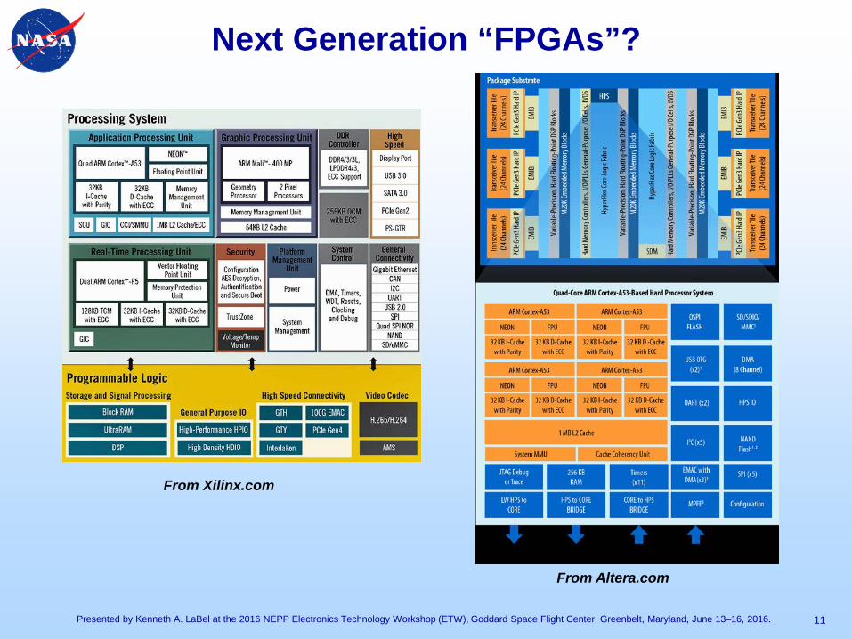
Next Generation “FPGAs”?
11Presented by Kenneth A. LaBel at the 2016 NEPP Electronics Technology Workshop (ETW), Goddard Space Flight Center, Greenbelt, Maryland, June 13–16, 2016.
From Xilinx.com
From Altera.com
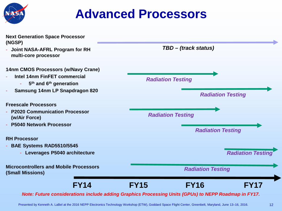
Advanced Processors
12Presented by Kenneth A. LaBel at the 2016 NEPP Electronics Technology Workshop (ETW), Goddard Space Flight Center, Greenbelt, Maryland, June 13–16, 2016.
FY14 FY15 FY16 FY17
Next Generation Space Processor (NGSP)- Joint NASA-AFRL Program for RH
multi-core processor
14nm CMOS Processors (w/Navy Crane)- Intel 14nm FinFET commercial
- 5th and 6th generation- Samsung 14nm LP Snapdragon 820
Freescale Processors- P2020 Communication Processor
(w/Air Force)- P5040 Network Processor
RH Processor- BAE Systems RAD5510/5545
- Leverages P5040 architecture
Microcontrollers and Mobile Processors (Small Missions)
Radiation Testing
Radiation Testing
TBD – (track status)
Note: Future considerations include adding Graphics Processing Units (GPUs) to NEPP Roadmap in FY17.
Radiation Testing
Radiation Testing
Radiation Testing
Radiation Testing

Commercial Memory Technology- collaborative with Navy Crane
13Presented by Kenneth A. LaBel at the 2016 NEPP Electronics Technology Workshop (ETW), Goddard Space Flight Center, Greenbelt, Maryland, June 13–16, 2016.
FY14 FY15 FY16 FY17
Other- MRAM (Avalanche STT, other)- FeRAM
Resistive- CBRAM (Adesto)- ReRAM (Panasonic)- ReRAM (Tezzaron)- TBD (HP Labs, others)
DDR- Intelligent Memory (robust cell
twinning)- 1xnm DDR3, DDR4, LP (TBD)
Hybrid or wide I/O- HMC, HBM, Wide I/O
FLASH- Samsung VNAND (gen 1 and 2)- Micron 16nm planar- Micron 3D- SK Hynix 3D, other commercial
Radiation Testing
Radiation and Reliability Testing
Radiation and Reliability Testing
Radiation and Reliability Testing
Radiation and Reliability Testing
Radiation and Reliability TestingRadiation and Reliability Testing
TBD – (track status)
TBD – (track status/test when available)
45nm options
Radiation and Reliability Testing
TBD – (track status or test)
Radiation andReliability Testing

Alternate Grade Electronics: Automotive
• NEPP has three goals for automotive electronics efforts– Determine exactly what:”automotive grade” does or does not
entail.• Includes understanding:
– Automotive Electronics Council (AEC) documents, and,– Manufacturer Production Part Approval Process (PPAP).
– Perform “snapshot” screening and testing on representative automotive grade electronics.
– Explore application of resilient automotive electronics system designs for space purposes.
14Presented by Kenneth A. LaBel at the 2016 NEPP Electronics Technology Workshop (ETW), Goddard Space Flight Center, Greenbelt, Maryland, June 13–16, 2016.
http://www.design-reuse.com/news_img/20141209_2.jpg

Small Missions/ Automotive
15Presented by Kenneth A. LaBel at the 2016 NEPP Electronics Technology Workshop (ETW), Goddard Space Flight Center, Greenbelt, Maryland, June 13–16, 2016.
FY14 FY15 FY16 FY17
EEE Parts Guidelines- Small missions (Class D, CubeSat
– 2 documents)- System on a chip (SOC) single
event effects (SEE) guideline- Board-level proton test guideline
Small Mission Commodities- See commodities roadmaps for
processors, memory, FPGAs, power
- CubeSat Star Tracker
Automotive grade electronics- Multiple classes of electronics
(passives, actives, ICs)- NASA and Navy Crane
- Freescale MPC56XX
Alternate system tests- Automotive resilience system
tests- Use of board-level testing for
screening and qualification - BOK
Radiation Testing
Reliability Testing
Radiation Testing Reliability Testing
Guideline development
Guideline development
Radiation Testing
Guideline development
Radiation Testing
BOK
Radiation Parts

Automotive -Advanced Driver Assistance Systems (ADAS)
for Space?
16Presented by Kenneth A. LaBel at the 2016 NEPP Electronics Technology Workshop (ETW), Goddard Space Flight Center, Greenbelt, Maryland, June 13–16, 2016.
From Freescale.com
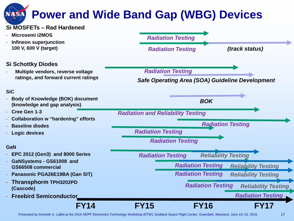
Power and Wide Band Gap (WBG) Devices
17Presented by Kenneth A. LaBel at the 2016 NEPP Electronics Technology Workshop (ETW), Goddard Space Flight Center, Greenbelt, Maryland, June 13–16, 2016.
FY14 FY15 FY16 FY17
Si MOSFETs – Rad Hardened- Microsemi i2MOS- Infineon superjunction
100 V, 600 V (target)
Si Schottky Diodes - Multiple vendors, reverse voltage
ratings, and forward current ratings
SiC- Body of Knowledge (BOK) document
(knowledge and gap analysis)- Cree Gen 1-3- Collaboration w “hardening” efforts- Baseline diodes- Logic devices
GaN- EPC 2012 (Gen3) and 8000 Series- GaNSystems - GS61008 and
GS66508 commercial- Panasonic PGA26E19BA (Gan SIT)- Thransphorm TPH3202PD
(Cascode)- Freebird Semiconductor
Radiation Testing (track status)
Radiation Testing
Radiation TestingSafe Operating Area (SOA) Guideline Development
BOK
Radiation and Reliability Testing
Radiation TestingRadiation Testing
Radiation Testing
Radiation Testing Reliability Testing
Radiation Testing Reliability TestingRadiation Testing Reliability Testing
Radiation Testing Reliability TestingRadiation Testing
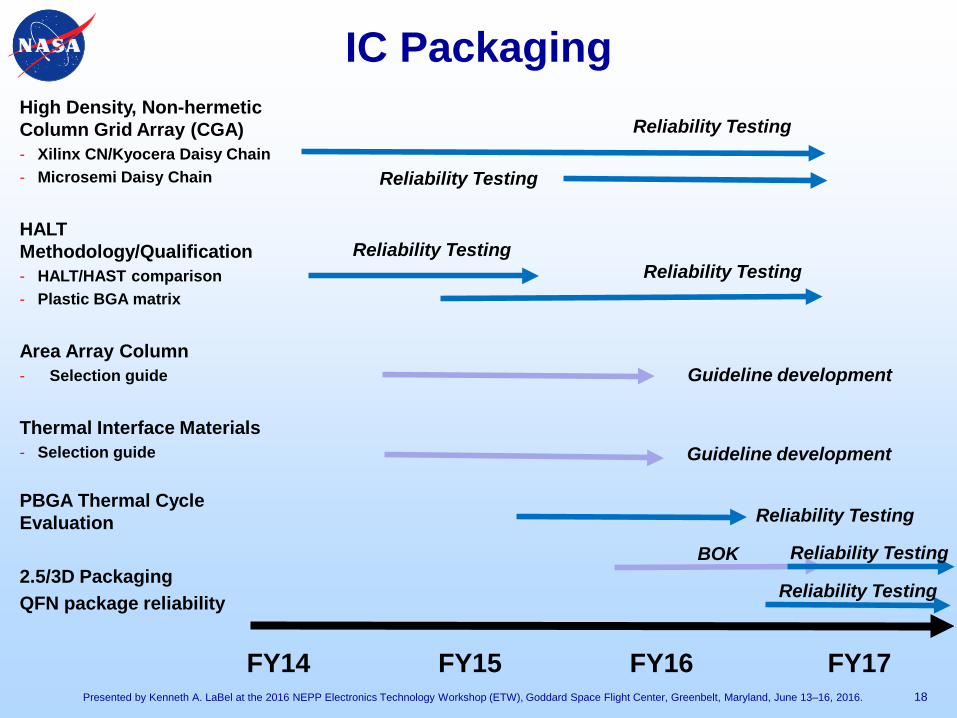
IC Packaging
18Presented by Kenneth A. LaBel at the 2016 NEPP Electronics Technology Workshop (ETW), Goddard Space Flight Center, Greenbelt, Maryland, June 13–16, 2016.
FY14 FY15 FY16 FY17
High Density, Non-hermetic Column Grid Array (CGA)- Xilinx CN/Kyocera Daisy Chain- Microsemi Daisy Chain
HALT Methodology/Qualification- HALT/HAST comparison- Plastic BGA matrix
Area Array Column - Selection guide
Thermal Interface Materials - Selection guide
PBGA Thermal Cycle Evaluation
2.5/3D PackagingQFN package reliability
Reliability Testing
Reliability Testing
Reliability TestingReliability Testing
Guideline development
Guideline development
Reliability Testing
BOK Reliability Testing
Reliability Testing

A Few Other Cool Tasks…
• CubeSat mission success/failure root cause analysis– Grant to Saint Louis University
• Using a model-based systems engineering (MBSE) approach to radiation assurance– Grant to Vanderbilt– Co-sponsored by NASA Reliability and Maintainability
Program– Uses a tool called “Goal Structured Notation”
• Keeping the CRÈME website alive– Support to Vanderbilt– Just standard maintenance and operation, no upgrades
• Proton test facilities– See poster on 6/14.
19Presented by Kenneth A. LaBel at the 2016 NEPP Electronics Technology Workshop (ETW), Goddard Space Flight Center, Greenbelt, Maryland, June 13–16, 2016.
Beyond Today – Sample Challenges• Complexity and sub-microscopic feature size issues for
inspection, screening, device preparation, and test– 2.5/3D Packages/ICs– Package on Package (PoP) Commercial Devices– FPGAs combined with an SOC– Cu Wirebonds– 14 nm and below feature sizes– ESD susceptibility– Trust
• Assurance– Automotive and catalog commercial EEE parts?– Increasing risk with a worldwide supplier base
• Traceability• Change control• Screening?
– Consolidation• What if the only source left is in an inhospitable or unauditable
part of the world?20Presented by Kenneth A. LaBel at the 2016 NEPP Electronics Technology Workshop (ETW), Goddard Space Flight Center, Greenbelt, Maryland, June 13–16, 2016.
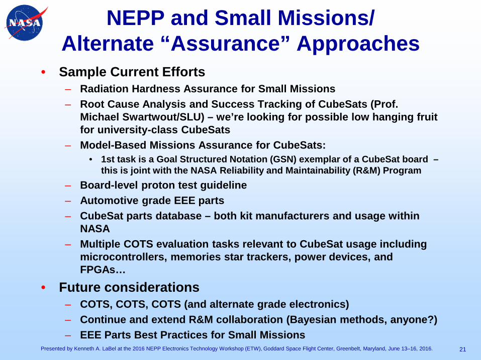
NEPP and Small Missions/Alternate “Assurance” Approaches
• Sample Current Efforts– Radiation Hardness Assurance for Small Missions – Root Cause Analysis and Success Tracking of CubeSats (Prof.
Michael Swartwout/SLU) – we’re looking for possible low hanging fruit for university-class CubeSats
– Model-Based Missions Assurance for CubeSats:• 1st task is a Goal Structured Notation (GSN) exemplar of a CubeSat board –
this is joint with the NASA Reliability and Maintainability (R&M) Program – Board-level proton test guideline – Automotive grade EEE parts– CubeSat parts database – both kit manufacturers and usage within
NASA– Multiple COTS evaluation tasks relevant to CubeSat usage including
microcontrollers, memories star trackers, power devices, and FPGAs…
• Future considerations– COTS, COTS, COTS (and alternate grade electronics)– Continue and extend R&M collaboration (Bayesian methods, anyone?)– EEE Parts Best Practices for Small Missions
21Presented by Kenneth A. LaBel at the 2016 NEPP Electronics Technology Workshop (ETW), Goddard Space Flight Center, Greenbelt, Maryland, June 13–16, 2016.

22
Summary and Comments
• NEPP Roadmaps and Tasks are constantly evolving as technology and products become available.– Like all technology roadmaps, NEPP’s is limited to funding
and resource availability.• Many other efforts are not being shown today (60+ tasks total)
– Partnering is the key:• Government,• Industry, and,• University.
• We look forward to further opportunities to partner.
Presented by Kenneth A. LaBel at the 2016 NEPP Electronics Technology Workshop (ETW), Goddard Space Flight Center, Greenbelt, Maryland, June 13–16, 2016.
https://nepp.nasa.gov