2011 FMS Program Notes and Comments - Entertainment Storage
21
Research Development Consultants Inc. Flash Memory Summit 2011 Notes © 2011 Research Development Consultants Inc. Page 1 2011 FMS Program Notes and Comments By Ron Dennison, Principal Consultant, Research Development Consultants Inc. 8/15/2011 Summary: This was the largest FMS ever with 5 tracks on 2 of the 3 days. I attended a variety of them and my notes and comments on the ones I attended follow. Some overall takeaways: 1. Cost is still the major issue limiting SSD adoption. 2. Reliability and endurance continue to be enterprise user concerns. 3. To address cost, MLC and even TLC (three level cell; 8 logic states) are on the SSD vendor’s roadmaps for the enterprise. 4. The controller and its FW continue to be the key to SSD functionality (there are still many shortcomings reported here) and lower cost using MLC and TLC NAND. 5. SSDs are an immature technology needing standards for testing, feature sets, operating systems, and reporting. 6. Automated Tiering and Caching SW are keys to adoption at both the client and enterprise level. 7. Several major SSD vendors have introduced enterprise class SSDs which run MLC flash well beyond the flash manufacturer’s endurance specification by using specialized signal processing and ECC methods in the controller. 8. To take full advantage of SSD performance potential, new interfaces and interface standards (some just emerging) are required along with new drivers. 9. As planar NAND flash technology scales to ever smaller nodes (1x already and soon 1y nm), a shift must be made to 3D structures (at 20 nm there are only about 10 electrons per state in the floating gate. TLC is 2x worse.) where there will initially be many 1000’s of electrons/state. Samsung, Toshiba and Micron are all well along on this. 10. Future technologies which challenge flash (RRAM, PCM, MRAM, etc.) are still many years away from taking the lead as flash goes 3D. Session F1C Enterprise SSDs Badridine Khessib - Microsoft SSDs in Large Scale Data Centers Summary: Need application specific endurance, no throttling, and rich set of S.M.A.R.T. counters Steve Hetzlers slide Relative $/Performance: Storage Chasm Dec 2008 from IDEMA VLDB 2010 TPCTC Workshop formula to calculate SSD benefits:
Transcript of 2011 FMS Program Notes and Comments - Entertainment Storage
Research Development Consultants Inc. Flash Memory Summit 2011 Notes
© 2011 Research Development Consultants Inc. Page 1
2011 FMS Program Notes and Comments By Ron Dennison, Principal Consultant, Research Development Consultants Inc. 8/15/2011
Summary: This was the largest FMS ever with 5 tracks on 2 of the 3 days. I attended a variety of them and my notes and comments on the ones I attended follow. Some overall takeaways:
1. Cost is still the major issue limiting SSD adoption. 2. Reliability and endurance continue to be enterprise user concerns. 3. To address cost, MLC and even TLC (three level cell; 8 logic states) are on the SSD
vendor’s roadmaps for the enterprise. 4. The controller and its FW continue to be the key to SSD functionality (there are still
many shortcomings reported here) and lower cost using MLC and TLC NAND. 5. SSDs are an immature technology needing standards for testing, feature sets, operating
systems, and reporting. 6. Automated Tiering and Caching SW are keys to adoption at both the client and
enterprise level. 7. Several major SSD vendors have introduced enterprise class SSDs which run MLC flash
well beyond the flash manufacturer’s endurance specification by using specialized signal processing and ECC methods in the controller.
8. To take full advantage of SSD performance potential, new interfaces and interface standards (some just emerging) are required along with new drivers.
9. As planar NAND flash technology scales to ever smaller nodes (1x already and soon 1y nm), a shift must be made to 3D structures (at 20 nm there are only about 10 electrons per state in the floating gate. TLC is 2x worse.) where there will initially be many 1000’s of electrons/state. Samsung, Toshiba and Micron are all well along on this.
10. Future technologies which challenge flash (RRAM, PCM, MRAM, etc.) are still many years away from taking the lead as flash goes 3D.
Session F1C Enterprise SSDs Badridine Khessib - Microsoft SSDs in Large Scale Data Centers Summary: Need application specific endurance, no throttling, and rich set of S.M.A.R.T. counters
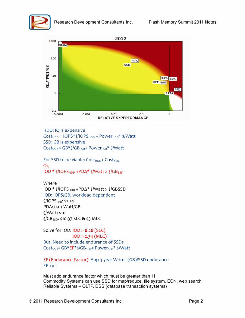
Steve Hetzlers slide Relative $/Performance: Storage Chasm Dec 2008 from IDEMA VLDB 2010 TPCTC Workshop formula to calculate SSD benefits:
Research Development Consultants Inc. Flash Memory Summit 2011 Notes
© 2011 Research Development Consultants Inc. Page 2
HDD: IO is expensive CostHDD = IOPS*$/IOPSHDD + PowerHDD* $/Watt SSD: GB is expensive CostSSD = GB*$/GBSSD+ PowerSSD* $/Watt For SSD to be viable: CostHDD> CostSSD Or, IOD * $/IOPSHDD +PDΔ* $/Watt > $/GBSSD Where IOD * $/IOPSHDD +PDΔ* $/Watt > $/GBSSD IOD: IOPS/GB, workload dependent $/IOPSHDD: $1.24 PDΔ: 0.01 Watt/GB $/Watt: $10 $/GBSSD: $10.37 SLC & $3 MLC Solve for IOD: IOD > 8.28 (SLC) IOD > 2.34 (MLC) But, Need to include endurance of SSDs CostSSD= GB*EF*$/GBSSD+ PowerSSD* $/Watt EF (Endurance Factor): App 3‐year Writes (GB)/SSD endurance EF >= 1 Must add endurance factor which must be greater than 1! Commodity Systems can use SSD for map/reduce, file system, ECN, web search Reliable Systems – OLTP, DSS (database transaction systems)
Research Development Consultants Inc. Flash Memory Summit 2011 Notes
© 2011 Research Development Consultants Inc. Page 3
SSD Endurance needs standards All current ones are inadequate: ignore IO block size and data retention (1yr min) Only OLTP-2 can last for 3 yrs w/o SSD replacement, not other apps! Mail, text search, decision support, OLTP-1 all fail BUT change assumptions and derive endurance experimentally. Brute force: random/sequential writes to check OEM spec. Result spec very conservative. Write amplification model graph. Data Retention in the Cloud is days not weeks: data is replicated across multiple servers, servers always on. Question: Can we push MLC SSD beyond per-spec 100% media wear? IE increase P/E cycles/cell? Answer: Yes, but answer detail is not known: Need S.M.A.R.T. counters: correctable ECC errors and free/retired blocks. Must Haves: % Media wear, host writes (GB) Like to Haves: free/retired blocks, FTL writes, ECC corrections Also Must Have:
No endurance or EOL throttling Secure erase TRIM command
Raymond Solone - Marketing VP STEC SSD Solutions as a Catalyst for Evolving Data Center Requirements Summary: Accelerate Access to Data by Auto-Tiering, SSD caching SW, PCIe solid state accelerators, lower cost with eMLC NAND [Marketing pitch for eMLC, STEC Controllers, S.A.F.E. and CellCare—RD]
How do we drive data storage efficiency: More and Now Consumer grade MLC is inadequate; need enterprise grade MLC or eMLC Consumer 20GB/day, Enterprise 8TB/day Write full capacity of drive 10x/day, every day for 5 years eMLC NAND 10-30k write endurance, plus controller ability- incl. extreme ECC 60k+ writes/cell 4th gen controller announced today by STEC; tradeoff slower erase time CellCare Technology for endurance; S.A.F.E. (RAID) technology Accelerate Access to Data Auto-Tiering, SSD caching SW, PCIe solid state accelerators Reduce costs by using the right storage for the right data
Esther Spanjer-SMART Modular Director SSD Marketing Differentiation in the SSD Market Summary: Can use MLC (vs. eMLC) in the enterprise with the right Controller/FW.
$30/GB in 2007 $1-$1.50/GB not that far off Higher endurance MLC usable in the enterprise Trade-off retention (1 yr not needed) for endurance eMLC 30k P/E cycles (due adaptive controller) Going to SSD optimized storage architecture 1.6TB 2.5” drives today SMART Modular, STEC and Anobit have announced products that overcome MLC flash endurance limits
Research Development Consultants Inc. Flash Memory Summit 2011 Notes
© 2011 Research Development Consultants Inc. Page 4
Adaptive Flash Management, Flash Guard, etc. is able to convert MLC to eMLC? SAS interface growing in importance Hockey Stick growth in coming years: ~12M units/yr by 2015?
Panel: Controller must be optimized for specific media-Raymond Tier 1 OEM support takes almost as many people as SSD development- Esther Cloud server $2000; eMLC too expensive – Badriddine Storage Infrastructure needs reoptimization for SSDs – Esther Write logging necessary for Random IOPS- Badriddidne
Forum F1A Pairing SSDs and HDDs in Computers Andrew Ku - Tom’s Hardware: Consumer & Enterprise Perspectives Summary: Consumers not adopting SSDs due to cost and enterprise due to limited reliability data and Cost. Editor, Bestofmedia Group [email protected], 661-412-2870, Besofmedia LLC, Culver City
Product evaluation person Cost is major issue Intel Ipeak Whitepaper 2011 Consumers willing to pay for performance, but only slight premium Consumer IO shifting toward video: Intel QuickSynch Architecture, Global Internet video 40% of internet Traffic Desktop: Tiered vs. Caching Notebooks: usually only 1 drive slot Consumers don’t care so much about ruggedness—most backed up to cloud Performance primary motivation for SSD adoption But long term Media Reliability not well understood: FW critical
Drive tester passes drive, but doesn’t work in system Replacement rate study on web site: SSD data not available beyond 2 yrs; linear model is graphing assumption, not supported by data Substitution effect: 1 SSD replaces 4 HDDs lowers effective failure rate HDDs fail more gracefully SSD failure is more binary Forget RAID; replicate data 3 times a la Google File System Enterprise adopting with caution, waiting for long-term reliability data Primary barrier to adoption is COST Data Center benchmarking varies with application Caching is fire and forget, but only improves reads; writes limited by HDD speed vs. tiered storage which improves both R/W
Charles Brady Foster – Intel, Client Side SSDs and Caching in the Client Segment Summary: Need to pair SSD and HDD to look like single drive with automatic SSD cache management but with GUI to manage.
Caching Configuration – Paired Storage (similar to nVelo Dataflex) SATA HDD + SATA SSD to look like single C: drive; seamless to user, improve system responsiveness by caching to SSD, lower average power consumption GUI for user to manage Ability to enable/disable caching as necessary (mainly to substitute new components)
Research Development Consultants Inc. Flash Memory Summit 2011 Notes
© 2011 Research Development Consultants Inc. Page 5
Cache asymptote 16-29GB; therefore SSD311 is 20GB Cache size option to use remaining partition as OS recovery or ? http://www,Intel.com/performance Significant performance and power improvements Intel “RST” technology
Q&A SSDs may eventually replace HDDs in some consumer applications; not soon Google docs and iCloud may limit local storage demands Paired storage just allows another cost tier
KN1: Yoram Cedar EVP & CTO SanDisk Cloud growth and Consumer use affecting demand Summary: Healthy demand growth requires continued scaling to have matching supply. Simple scaling approaching asymptote and will give way to 3D structures.
[Enterprise and Client] 33% of NAND bits in market in mobile devices in 2015 15% in tablets in 2015 25% in SSDs [7M in enterprise in 2015] 26% Other established end markets In short, healthy demand growth Supply Growth Flash scaling reaching asymptote: Therefore supply growth rate lower, also market larger than in past so % increase take more capital and equipment Limitations in flash scaling physics require adaptive management controllers Therefore moderate supply growth with solid demand drivers Forward thinking One more immersion lithography scaling after 19nm Therefore vertical NAND to re-use FAB resources and current lithography tools 3D RRAM shows best promise for a scalable post-NAND technology—will require EUV tools 23% CAGR for flash vs. 4% thru 2015
In future, 64Gb and 128Gb dice will be available from various vendors KN2: Eric Kao Memoright The age of application specific SSDs Summary: HDDs are simpler and more stable than SSDs but are tailored to specific applications. SSDs need to be too.
What makes SSDs more application specific than HDDs? FW defines personality 4 case studies No one talks about application specific HDDs HDDs more stable than SSDs SSD latency a very complicated picture Personality of SSD must match demand from host SSD is actually a large array of drives with 100s of flash chips: job of controller is to maximize utilization-performance
Research Development Consultants Inc. Flash Memory Summit 2011 Notes
© 2011 Research Development Consultants Inc. Page 6
Conflict Flash blocks like to be written in full due to block erasure nature, But interleaving scheme likes to write across as many blocks as possible, thus creates fragmentation. Computation time required to find block to be erased/recycled. Case 1 Video editing HDD and SSDs give similar performance after SSD cliff Case 2 Main Stream PC Bench mark with PC Mark Vantage 3 Wide spread of latency OK Case 3 RAID Array Random IOPS, narrow spread latency, high reliability and endurance Low write amplification Case 4 Linear Drive (tape substitute) Pure sequential write by super blocks, random page read, high MTBF Case 5 Tablet PC Answers TBD due varying workloads BER vs erase cycles tPROG vs P/E cycles Change file system structure to favor flash?
KN3: Glen Hawk Micron The Alchemy of NAND flash Summary: NAND is approaching wall [asymptote]; need to go through or over with 3D processes and ultimately PCM.
Newton As alchemist; good from pursuit of impossible 25.7 Exabytes 2000-2010 shipped 57.8 EB 2011-12 Micron very happy about cloud—due potential data center growth ClearNAND storage on PCI card Memory wall – plan to jump over wall (or open door) Think intelligently (getting full performance from 20 nm NAND is challenging) Embedded MMC is fully managed solution, ECC free, System level (SSD) SATA and SAS are just beginning PCIe, etc.? Today’s NAND is 2D: 3D NAND Micron is working on is solution— picture 3D NAND when first deployed may hav 10k e- per gate vs 20! In initial designs Relaxed design rules Ancillary functions smaller part of die Smaller die size Capacity boost/cost reduction PCM also in future 3D is a couple of years away from production
Session 105 SSD Testing and Benchmarking Marty Czekalski, STX Summary: Current SSDs have many controller/FW related artifacts and need extensive and proper benchmarking/testing to verify application suitability.
Research Development Consultants Inc. Flash Memory Summit 2011 Notes
© 2011 Research Development Consultants Inc. Page 7
Use cases Persistent Storage Cache Extension (L3 Cache) Traditional Tools
SNIA PTS IOMeter Database Office SPC-1C (small systems or individual drives); Storage Industry De Facto Bench Mark
Proven Sustainable Repeatable 60% writes, 40% reads
Audit of other drives “SPC-1C-like” Precondition to steady state SPC asks for 8 hour pre-run now
Client drive 2.5ms @ 150 IOPS; another 2.5ms @70 IOPS; Another took a 4 hour “rest” Notebooks have bursty workload which enables use of these drives; enterprise demands SPC testing over extended periods of time (artifacts at 3-5days)
Easen Ho, CTO, Calypso Summary: Testing is essential to verify SSD functionality. Some emerging and potential tests are reviewed.
Difficulties NAND SSDs are complicated (controller and FW) Difficult to get people to agree on tests Write history: how much written and where Where is data curr3ently written Nature of data 100% (user) real world, not very useful because difficult to generalize Trace based capture and playback Trace based playback: AnandTech Storage Bench, Drivebench Scripted application playback tools: Sysmark, PCmaRK Synthetic Stimulus: Calypso CTS, SNIA work in progress,
SNIA SSS V1.0 Purge Set Conditions Pre-Condition Run until Steady State Report format
Some Emerging Tests: Demand Intensity:
Vary total outstanding IOPS: RND 4k writes Response Time Statistic: Response Time Histogram
RND 4k writes until Steady State Cross Stimulus Response:
Write SEQ128K; Sw to RND4K; then back to SEQ128K Long Recovery Times
Research Development Consultants Inc. Flash Memory Summit 2011 Notes
© 2011 Research Development Consultants Inc. Page 8
Idle Recovery: (garbage collection metric) RND4K writes then idle for various periods then resume
Other potential tests Energy efficiency Data compressibility Enterprise workload
Doug Rollins, Sr. Applications Engineer, Micron Summary: SSD performance is time and history sensitive. Perform testing in a consistent manner to get consistent results [Simple benchmarks may not reflect real world workloads and consequent performance— RD]
Performance varies with time but approaches asymptote after some time FOB, transition, steady state (SNIA PTS) Enterprise Assumptions
Always full Always being accessed Decisions made on steady state performance Steady state ≠ full drive ≠ worst case
Steady State from SNIA PTS Full Drive Defined Worst Case Defined To get consistent results
Always start from a known fixed point Always precondition the drive in the same way Always stimulate the drive with a single, fixed stimulus until steady state is reached
Example test sequence for every stimulus of interest Purge, SE, or LLF Precondition Stimulate until steady state is reached All are measured full span Ensure the host does not impede performance
Frank Shu, VP R&D, Allion Test Labs The Myth of SSD Testing Summary: Review of factors examined and data generated by Allion in SSD testing.
Factors NCQ Queue depth TRIM implementation: TRIM implementation can choke IOs Honoring Flush- Not all SSDs with volatile write cache honor Flush Differing power implementations: On-Off vs On all the time Use temperature to accelerate ECC errors: most data miscompares occur below 25C or above 70C.
Session 10 Standards Kevin Marks Principal Engineer/Technology Strategist, Dell and Peter Onufrykl, IDT PCIe as an SSD IF [Pitch for NVME— RD]
Going from 2.5 to t to 8 GTps; low cost; power management incorporated NVMe—NVM Express: Standardized drivers, consistent feature set, industry ecosystem
Research Development Consultants Inc. Flash Memory Summit 2011 Notes
© 2011 Research Development Consultants Inc. Page 9
NetApp, EMC driving standard NVM Express 1.0 completed March 1, 2011 nvmexpress.org Windows driver in dev. ( NVMe Spec Queing Interface Command Sets (Admin and IO) Commission Queues, Head, Tai8l
Harry Mason, LSI & Marty Czekalski, STX SAS Anchors Enterprise SSD Adoption [Pitch for SAS IF]
SAS RAID outperformed PCIe drive (details?) MultiLink SAS coming
Jay Neer, Molex and Galen Fromm (HS signal integrity) Connector evolution [Review of Development Connector Status]
The mating IF is fully defined The device side connector mounting is undefined SAS 3 losses similar to 40G Ethernet
Roland Schuetz, MOSAID Technologies HLNAND2 (up to DDR800) [Pitch for MOSAID HLNAND2— RD]
External IF chip to controller Synchronous clock 1.2V IF MCP package die stack
Tutorial 1A Next Gen Controllers Moderator: Chuck Sobey Tong Zhang, Renssaler Polytechnique Institiute Self Healing SSDs [Interesting Academic Research Project— RD]
Scaling reducing reliability, increasing noise HDDs same issue; solution channel & controller: Need to understand details of device characteristics Then have device aware SSD system P/E cycling increases charge traps; reduces noise margin until ECC tolerance limit is reached Two trap types: Oxide trap, Interface state trap (recovers over time and at higher temperature) Explicitly Leverage this wear out recovery phenomenon in FTL: rethink over-provisioning and temp Solution: Put heater under flash dice. Before heating move data to backup. Sequence recovery Modeled to investigate potential Takes significant power to achieve high temperatures 3.5W for 200C and 35 min to recover 80% of IF traps (5W for 250C) Backup impact on performance can be minimized by doing during idle times (halt during IO request) DiskSim to simulate system operation: impact on system performance minimal with small granularity of backups/heatups
Research Development Consultants Inc. Flash Memory Summit 2011 Notes
© 2011 Research Development Consultants Inc. Page 10
Kent Smith, Marketing, SandForce Garbage Collection, Foreground vs. Bkgd Summary: Effect of TRIM command and “DuraWrite”.
Wikipedia Garbage Collection article pictures OS deletes file but doesn’t tell drive until overwrite command Result: increase in Write Amplification: Soln—TRIM Command TRIM command sent at point of file deletion
Prevents GC on invalid data Increases free space known to SSD controller
TRIM Benefits Higher throughput Improved endurance Lower WA
Doesn’t work behind RAID Example DuraWrite: SandForce’s proprietary lossless compression improves free space Background GC moves “soon to be deleted” data which may impact performance Foreground GC with TRIM higher performance
Ariel Maislos, President and Founder, Anobit New Era in Embedded Flash Summary: The reduction in process node is driving exponential growth in ECC sizes and complexity required. The effect of managed and half-managed flash on controller architecture and capability.
Editor for 802.3 Ethernet standard Chart ECC, P/E cycles vs process node Exponential curve in ECC complexity required Architecture is changing: Application controller no longer directly connected to raw NAND media Half managed (EZ-NAND, Dual DDR) or Managed NAND (SATA, eMMC, UFS) [PCIe can be either] Dealing with raw NAND on system side is too complex Q. Clear NAND: below 30nm most NAND is half or fully managed
Marc Acosta, Marketing but Office of CTO, STEC SSD Controllers for Enterprise Summary: STEC rises to the challenge with proprietary technology.
8 patents, EE UCI Avid yachtsman Quote from IBM J R&D 2008 Rich Freitas: Issues with NAND Flash Write Performance Challenge
Log structured file system to turn random access into sequential access (Berkeley 1998) DRAM Write back cache Enable usage as Tier 0 storage
Cost Challenge 1 bit/cell SLC Large geometry flash FPGA based platform MLC issues: slow write, low write endurance higher BER
Research Development Consultants Inc. Flash Memory Summit 2011 Notes
© 2011 Research Development Consultants Inc. Page 11
Solutions: interleave support, CellCare Result: 5 yr warranty at 10x writes/day Claim: MLC drives outperform many SLC drives MLC challenges: high flash failure rate, data retention, read disturbance Solutions: parity protected data, advance firmware FPGA Challenge
Changed to ASIC: advanced power management, advanced ECC (higher code rate) Outer layer CRC protection (appended on receipt from host and checked on return to host)
David McIntyre, Altera Flash Controller Solutions and Programmable Technology Summary: PLDs offer flexibility in design needed in rapidly changing market.
PLDs – CPLD & FPGA Lower Risk, faster time to mkt Being used today in 100’s k unit applications Uses 28-22 nm process nodes vs 90nm for ASIC May use High Performance or Low Power platform PCI gen 3 and SAS/SATA 6G support available Soft vs Hard IP: Hard improves device speed and BW of IF Storage Target Apps
Flash Cache/SSD RAID Bridging Bride Plus ASIC Replacement
Flash Controller Design Challenges Emerging Memory Types ECC going to BCH IF Support PCIe, SAS/SATA, FC, IB
Examples Violin Denali
28nm today Uncertainty and Change favors PLDs Many Flash Cache Applications 200MHz clock speeds at 28nm
Eitan Yaakobi, Grad Student [now post doc] UCSD ECC Codes for TLC Flash Summary: A new ECC encoder-decoder scheme for TLC is proposed.
Very bright personable guy, new PhD New proposal for TLC ECC beyond BCH, LDPC 3 pages from each level set MSB, CSB, LSB blocks Experiment: erase, write, read MSB pages have best error rate within block Instead of throwing high error block away, store only 2 bits in cell or 1 bit Errors are corrected independently Goal: correct errors in a group of pages together: if a cell is in error, then with high probability one of the bits in the cell is in error
Research Development Consultants Inc. Flash Memory Summit 2011 Notes
© 2011 Research Development Consultants Inc. Page 12
Encoder to group three pages into one Goal in decoder to clean up single bit errors improving overall error performance March workshop
KN4: It's Not Your Father's Hard Drive Or Is It? John Scaramuzzo, SMART Modular Summary: To get further market penetration in the enterprise SSDs must use cheaper MLC media. To do this and have sufficient endurance, MLC must be operated beyond the manufacturer’s specification using additional signal processing and ECC in the controller.
Tremendous improvement in IOPS of SSDs creates a new storage class that is just being implemented in applications: Examples Barriers to wider adoption: infrastructure and cost Read mostly SSDs are driving boot and entry server adoption 7-10 drive writes/day is mainstream workload; SLCs too expensive, eMLC OK eMLC is screened and tested differently but adds cost Solution: use plain MLC flash and increase endurance enough to work in enterprise As technology node gets smaller, additional ECC is not enough Solution: additional signal processing with added ECC Take advantage of population statistics Operating beyond raw flash spec by tuning flash parameters throughout the SSDs life Parameters: ? Q. How do you handle differences in suppliers products; no standards? No good answer. Need understanding of products and good test strategy for result Q. Certification of SSDs? Standards helpful, but too many market application variations.
KN5: Mythbusting Flash Performance Bill Nesheim, VP Solaris Platform Eng., Oracle Summary: SSD has great performance but the technology is immature. There are issues with performance, performance predictability, response time predictability, R/W asymmetry, reliability, and standards. [This was probably the best keynote of all, since it took real user data and gave a call to action and do list to the SSD manufacturers—RD]
Ex-SUN Is there anything beyond IOPS Oracle flash integration Half of Flash $ market in enterprise, IDC; 51% CAGR thru 2014 ZFS filer uses flash, OLTP and DB run faster with flash, customers wan SSDs, PCIe cards and flash arrays (easier to service, hot swappable) Flash in all Oracle systems (improves data waits, particularly read waits): Exadata, Exalogic, and ZFS Storage Applicance all have designed in flash DB Flash Cache—principally improves read performance Customer Example: SQL DB access 3M waits in 15m = 9.5 hours actual wait time Deployment issues: Can be slower than with HDDs; requires engineered system approach 5.3 TB PCI flash to 100-336 TB HDD in Oracle Exadata DB server Issues Substantial Performance Variability, especially 100ms to 1s outliers; low as 54 IOPS; R/W BW variation: can be worse than disk! Per slot power limitations Challenging environment for supercaps and batteries
Research Development Consultants Inc. Flash Memory Summit 2011 Notes
© 2011 Research Development Consultants Inc. Page 13
Unpowered data retention constrains use as archival media Varying and unique failure modes It’s really not just IOPS Overall response times important Limited application threading Outlier response times killer Need:
More predictable performance More predictable response times Less R/W assymetry
Example of lousy all write workload Basic parallel computing problems When IO is slow to return is like accident on 101, queue builds up with repeated requests for same data Difference in real performance due to slowest 1% of IOs Example of 2.5x impact on volume of flash needed in system MLC more expensive than SLC from a $/Endurace view Device with embedded service policy can be a killer Issue: standards or lack thereof Current compliance isn’t Device should correctly report Read Capacity or ATA Identify Device correctly Conclusion: Technology Immature
Performance variability and predictability Issues Reliability and Availability Issues Standardization needed
KN6: Emerging Challenges in NAND Flash Technology Seaung Suk Lee, VP Flash Product Planning, Hynix Jeff Janukowicz, IDC intro Summary: Review of NAND flash technology roadmap and changes needed. [This was an excellent technical presentation with many useful slides but as of 8/15/2011 the presentation has not been posted online—RD]
Market overview $25B this year 29B in2014 Mobile, Tablet, SSD major growth areas; biggest SSD Going forward Increasing performance and reliability require controller+SW advanced Scaling limitations: Physical: patterning, structure formation (FG,CG,IPD,..) Electrical: interference, capacitive coupling ratio, # of e- in FG, dielectric leakage NAND program speed strongly related to bit line and word line loading WL matl W (tungsten), was Co or NI silicide, previously polysilicon WL space air gap to replace low-K dielectric BL matl Cu BL space air Too few electrons in FG with scaling Vt distribution now has overlap in smaller geometries E2NAND has embedded ECC Future Technology
Research Development Consultants Inc. Flash Memory Summit 2011 Notes
© 2011 Research Development Consultants Inc. Page 14
Planar FG with High-K dielectric; problem dielectric not stable 3D structure Options:
Samsung and Toshiba announcements in 2009 To overcome deep poly-Si channel requirement change to horizontal Dual CG and surrounding 3D FG cell Epi Si Pillar 3D structure
Good final comparison slide of various 3D structural announcements KN7: The Next Frontier in NVM Performance Knut Grinsrud, Intel Summary: To get the next 20x in storage performance need NVMe, much lower power. Knut has a lab HW/SW demo running.
Intel Fellow leading small SSD architecture group SSDs have given us 20x in storage performance The next 20x? 300 simultaneous videos at full HD videos in single display browser (1.02M IOPS) Enablers 8x PCIe Gen3 physical IF NVMe logical IF (nvmexpress.org) New driver stack for 1 M IOPs Low Power another requirement Thus need 20x lower power state than current (5mW in 50ms of resume latency) between current low and off states (graph of resume latencies and lost time) New SATA draft low power state proposal NVM + HDD graph PCIe + AHCI for high performance for client in addition to PCIe + NVMe
RRAM Session 205 Summary: Various new and emerging RRAM technologies are showcased. [Most are still in the lab, a few are pre- or very small volume, early production. New system solution, signal processing and ECC are needed for these new memories and these will also take time to achieve commercialization.—RD] Moderator: Alan Niebel, Web Feet
RRAM technology variations Narbeh Derhacobian, Adesto Technologies CBRAM Memory
Conductive Bridging RAM (Adesto founded 2007) Apollo 1st commercially available ReRAM Memory (eng samples now, customer samples 2H2011; 1Mb device) Like SONYs technology Process variation can vary device characteristics over wide range Now >90% die yields; some 100% yields with built-in redundancy 34 patents issued, 45 licensed patents, 42 in process Done in 2 different CMOS fabs with no cross contam. 130 nm node
David Eggleston, Unity Semiconductor Emerging Memory for the Cloud
CMOX – insulator and conducting metal oxide 2015 Cloud requires Millions of IOPS
Research Development Consultants Inc. Flash Memory Summit 2011 Notes
© 2011 Research Development Consultants Inc. Page 15
Cloud Attributes Tb on single chip 100’s of MB/s (500 R, 200 W) Easy ECC Low Cost
CMOX 100x faster than NAND PC 8F cell size issue MRAM too expensive RRAM not stacking yet, high write current, reliability Memristor ? NAND slow and hard to use but capacity and low cost Two layers demonstrated 10k to 100k cycle life goal of current PCRAM has missed product window! Paper on physics from 2008 downloable from web site Commercialization in 2014-2015
Janice Nickel, HP Labs Memristive Memory
Heads JV w Hynix Leon Chua at UCB: flux, V, q, i Flux to charge relationship Pinched loop iV curve Pt. TiOx(x≈2), Pt sandwich Get this presentation Endurance to 1012 cycles at Samsung 100’s of ps to switch; 10+ years life; Hynix partner at 50nm node 5 levels shown in lab in single cell Materials used determine retention TaOx paper to be published 1H2012 should see first real devices; Commercialization in 2014?
“Amigo” Keiici Tsutsui, Sony Characterizing ReRAM for NVM Cache Applications
Structure: CuTe = Cu+ source layer Few nm of insulator (Cu filaments grow in this) Lower electrode
Demonstrated: 2.3GB/s read, 216MB/s write, 1M program cycles Goals:
Cost ~ same as DRAM (6F2) Capacity ~ same as DRAM Read 5GB/s, Write 500MB/s
4 levels of resistivity reported 2007 but not commercially MRAM Session 208 Summary: Various new and emerging MRAM technologies are showcased. [Many, like the RRAM or ReRAM are still in the lab, a few are small volume, early production. The exception is Everspin which is projected to ship 3M units this year.—RD]
Research Development Consultants Inc. Flash Memory Summit 2011 Notes
© 2011 Research Development Consultants Inc. Page 16
Toshiba and Hynix Agreement on STT-MRAM, Grandis Acquired by Samsung July 22nd Rajiv Ranjan, CTO, Avalanche Technology
Ex-STX, Komag Founded 2006, VC Patented low power MTJ plus patent pending cell design plus systems design approach Switching demonstrated at 300ps, but Perpendicular below 1ns Deposit MTJ’S as part of back-end process SRAM replacement; 15f2 cell size in 64Mb chip using 65nm CMOS to be first commercial chip Thinking 8 f2 possible 3D Stacking available
Barry Hoberman, Marketing, Crocus Technology The path to Gigabit MRAM
Closed $300M deal with Russian company to build fab there Magnetic Logic Architecture—Thermally assisted switching (TAS) Self differential sensing (allows broad range of junction resistances and resistance deltas) High temperatue operation Simplified processing Broader yield curve No magnetic anneal Reference pinning layer with its Pt gone NAND w 8x MLC And 2 layer structure to offset 25 f2 cell size Zero Knowleddge Proof secure implementation
Steffan Hellmold, Everspin Industry first and leading supplier Shipped 3M pieces, will ship >3M in 2011 alone 600 active patents and applications Spin off from Freescale in 2008 50ns R/W latency Cycling endurance 1015 cycles > 20yr life Instant on/off 50us, 50ns Temp range -40 to 150C Ultra low radiation induced SER Easily integrates with CMOS logic History 4x every 12-15 mos Toggle MRAM TAM $500M of total $80B memory market Markets: Industrial, Datacom, POS, Energy, Transportation (Auto and aviation), Storage and Servers (metadata, SRAM replacement) Not shipping STT MRAM yet, but plans on track
Jay Kamdar, MagSil MIT roots; Key HDD licensees in last 2 years Solves write current and scaling(180nm to 18nm) issues Optimized magnetic stack Fabless IP company MTJ is used only as sensor—has storage media
Research Development Consultants Inc. Flash Memory Summit 2011 Notes
© 2011 Research Development Consultants Inc. Page 17
10 f2 cell Commercial in 2013 from consumer OEMs
Steve Clidakis, Spin Transfer Technologies skipped
New NVM Technologies Session 303 Summary: More alternatives to MRAM and PCRAM are reviewed. Moderator: Jim Cantore Greg Atwood, Senior Fellow, Micron Current and Emerging Memory Landscape [Good overview of the flash roadmap and PCM technology—RD]
Memory moving from support role to a defining system role Scaling planar NAND is becoming more difficult: few electrons, capacitance limitations, tunnel and interpoly charge retention, voltage limitation, etc. Storing 10 electrons/state in MLC At 20um No brick wall but increasing complexity Good Roadmap slide [not available as of 8/15/2011-- RD] 3D options: Deck-by-Deck, Vertical NAND (most work here), Crosspoint True NAND successor needs to Be MLC capable, 3D stackable, simple process flow, scalable, reliable, performance and power NAND successor not the only target Storage Class Memory Explosion of new memory concepts – good summary slide [also not available as of 8/15/2011-- RD] PCM Xtalline low resistance phase, amorphous high R Cell 1 diode, 1 resistor More attractive as cell size shrinks due smaller volume of material heated Good for execute in place (XiP) semi-static data Cross point memory simple 4 f2 cell divided by number of layers plus allows peripheral elements underneath all Example PC-base x-point memory at 64Mb
Thomas Rueckes, CTO, Nantero High Reliability Carbon Nanotube NRAM
Post NAND, post DRAM, NRAM for NVM (low cost, reliable) Scalability to <5nm, low write i, Dense 1T1R & 1D1R, MLC capable Founded 2001; sold govt. business to Lockheed Martin in 2008 Now development and IP licensing model with unannounced commercial development partners W and TiN used with C nanotubes; simple well understood material Set is electrostatic (low R), Reset is phonon heating driven (high R) using short, high rise time V pulse (stable at 300C for hours) Spin on colloidal CNT, trace metal clean, metalize, patterned currently with 193nm dry and immersion lithography, CNT integration temperatures 425C (works to 700C with W interconnect), CNT and metal RIE etch to complete pattern
Research Development Consultants Inc. Flash Memory Summit 2011 Notes
© 2011 Research Development Consultants Inc. Page 18
140nm 4Mb sample devices available 100kohm on 100Mohm off Data retention 10yrs .01fJ/nm2 switching energy Activation energy 4.5eV allows stability at 300C for many hours Emprirical data for 1B cycles expect unlimited No HV transistors required due low switching currents 20ns writ and re3ad
Alex Zettl, UC Berkeley (LBL Grad Student, advisor Alex Zettl) Billion year, Ultradense Memory [Years away from potential uses—RD]
Works with grapheme and CNT in nano-electromechanical systems (NEMS) Position based storage a la Abacus Fe Nanoparticle sliding within CNT (Pd contacts on Si3N4 base on Si 100 nm long CNT 10=-20 nm wide, voltage 1.5 to 1.7 volts to move 25um/s Del R/R ~50/5600 ohms or ~1% Del Energy ~1.5-1.7 eV resulting in dwell time fo >109 years at 300K Aligned CNT “forest” Getting Fe into CNTs is challenging Mechanism of motion: Electromigration or e- wind? R Effects: intershell coupling perturbation, geometry effects, e- resonance effects? Research continues Multistate, CNTs with fewer walls
Luc Thomas, IBM Almaden Racetrack Memory
Stu Parkin’s group Now working on Horizontal Racetrack Memory Both soft magnetic material in plane and hard magnetic materials in perpendicular mode STT sensor: change in spin angular momentum of electrons moving thru wall can move domain wall MTJ (TMR?) sensor to sense direction of magnetic moment 108 A/cm2 12umx150nmx20nm NiFe nanowire shift register; del R 0.2 ohm Hall bar Del R/R 0.1/1220; Hall bar better noise level 250uA switching current 2ns write with <4pJ, sub-10ns readout Working on vertical racetrack
Future of PCM Session 306 Summary: PCM progress review Chair Sean Eilert, Micron
Greg Atwood, Micron
Condensed Reprise of previous sessions presentation
Minghai Qin, CMRR UCSD (Grad Student) Constrained Codes for PCM
PCM allows single cell access vs NAND string
Research Development Consultants Inc. Flash Memory Summit 2011 Notes
© 2011 Research Development Consultants Inc. Page 19
PCM ~108 cycles Endurance ~ 300 yrs Heating affects cell performance and adjacent cells Therefore need Modulation code with time and space constraints Suggested coding to limit single cell consecutive writes, writes to consecutive cells, total cell rewrites (α, β, γ) To be Published in Globe Com 2011 Some results related to write once memory codes
Mike Strickland, Altera Read latency close to DRAM Write 10x worse than DRAM but 100x better than NAND 100x better endurance Low idle power Cache for Enterprise either as a hybrid with flash or later As cache Initial hybrid uses: Metadata/logs, RAID parity, write thru cache DRAM cache in conjunction with PCM? Today useful for mobile devices Shorter term – hybrid Longer term – general cache as price comes down and capacity goes up Issues: Uncertain forecast, differentiation, high ASIC development costs
Gary Kotzur, Dell No slides; better not to leave paper trail! NAND running out of steam; performance (read and write latency), endurance Important system level TCO metrics: $/IOP, W/IOP, $ Near term PCM Issues/Possibilities
Pros: Write endurance, high read performance (low latency); No erase before write (no GC!—especially important for RAID) Cons: Power, Write power Write back cache; Hybrid
Longer term Need to reduce power to allow higher density with reasonable power envelope Write and read asymmetry 20x today, need 4x Need densities approaching flash Need cost approaching flash
Less controller management is attractive to reduce latency outliers Larger page sizes of NAND are unattractive; smaller blocks! Initial apps OLTP, DSS, Financial, Oil & Gas Latencies induced by “stacking of devices” can be reduced by PCM
Panel Discussion: Scaling will benefit power due less joule heating required for write Consistency in performance is very important (latency outliers, GC) Smaller granularity also advantage WA=1! Energy/current densities not near any material limits Cost per bit 45nm 1Gb is state of art PCM vs 20nm 64Gb NAND More targeting DRAM than NAND today
Research Development Consultants Inc. Flash Memory Summit 2011 Notes
© 2011 Research Development Consultants Inc. Page 20
KN8: How Enterprise SSDs Can Revolutionize the Data Center Scott Stetzer, VP Technical Marketing, STEC Summary: Demand is great. To achieve necessary cost, must use MLC and TLC. The controller is the key to this along with auto-tiering SW.
WD, Maxtor, Quantum Change in last 3 years from300 to 80k IOPS, Tier 0 storage, SSDs main emphasis Auto tiering SW Bringing MLC into enterprise just beginning; needed for cost Controller [and FW] is key to intelligent system use of NAND flash Technology shifts drove out suppliers in HDD markets Good slide showing HDD vs SSD supplier numbers [not available as of 8/15/2011-- RD] Increase in technology demand with decreasing node size will shake out suppliers unable to keep up with controller technology demands e-MLC gets endurance advantage by slowing down—wrong direction Need to use ordinary MLC with capable controller 1.8ZB discussion [cribbed from EMC study] $49B server platforms, $28.7B storage platforms (IDC when?) Substituting SSD for HDD requires auto tiering need similar caching app for servers; accelerating time to data from 10’s of ms to 10’s to 100’s of us; goal 2-10x performance improvement at ½ price [assumes replacement of 600GB, 15k rpm enterprise class drives with near-line capable 2TB, 7200 rpm drives!!] Modernize SAN using auto-tiering SW again replacing most 15k drives with 7200rpm 2TB ones. SSDs are catalyst for Cloud Enabling all SSD storage platforms: lower cost thru MLC; TLC! Need $1-1.50/GB and tiering using mix of SLC, MLC, TLC
KN9: SSD vs. HDD vs. Hybrid: It's Not Who Will Win, But Who Should Win John Moon, Sr. Director Emerging Systems, Seagate Summary: HDD and SSD manufacturers need to cooperate to define standards, OSes, etc.
1M Hybrid drives shipped Lead designer for Momentus XT Each type has advantage for specific market/application Work together, don’t re-invent the wheel
1970 ECCs 1985 DRAM buffers 1986 Read retries 1992 Auto reallocation of bad sectors 1995 S.M.A.R.T. 2000 Background activities: offline scan, data refresh 2009 LDPC
Demonstrate the truth: benchmarks should reflect user experience Benchmarks that reflect end user experience needed; Sysmark not good enough Need to be easy to understand System independent? Repeatable results Your friend can be my friend; we all need to talk together
TRIM works with Hybrid but Microsoft didn’t work with HDD folks TRIM would also help HDD RPM detect
Research Development Consultants Inc. Flash Memory Summit 2011 Notes
© 2011 Research Development Consultants Inc. Page 21
Defrag uses varies across all three Hints for ordering writes System pre-fetching Hibernate, Sleep, Resume File aware information
Can we share the same menu? Reliable MLC and TLC Common interface Common error handling: ECC retries, signal proc Speed Capabilities; page sizes, # of planes, program and erase times
More work together is needed Good quote: If you want to be incrementally better: be competitive. If you want to be exponentially better, be cooperative. Source unknown [email protected]