2. Intrinsic semiconductors
36
Institute of Solid State Physics Technische Universität Graz 2. Intrinsic semiconductors Oct. 9, 2019
Transcript of 2. Intrinsic semiconductors

Institute of Solid State PhysicsTechnische Universität Graz
2. Intrinsic semiconductors
Oct. 9, 2019
Atoms are arranged in a periodic pattern in a crystal.
The atomic arrangement affects the macroscopic properties of a material.
Many important materials (silicon, steel) are crystals
Crystal Structure
Insulin crystalsGallium crystals quartz

Crystal Structure
face centered cubic, fcc
body centered cubic, bcc
simple cubic
basis
Bravais lattice Crystal
= +

Crystal planes and directions: Miller indices
MOSFETs are made on <100> wafers
[ ] specific direction< > family of equivalent directions( ) specific plane{ } family of equivalent planes
A plane with the intercepts 1/h, 1/k, 1/l is the (h,k,l) plane.

http://lampx.tugraz.at/~hadley/memm/materials/silicon/silicon.php
silicon
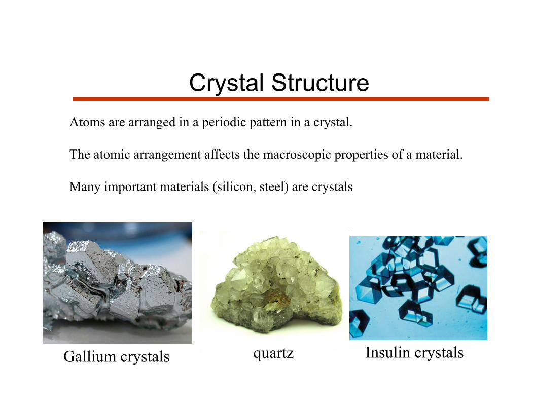
Silicon surfaces
(Source: Sandia Nat.Labs.)
Si(100)
Si(111)

KOH etches Si {110} > {100} > {111}, producing a characteristic anisotropic V-etch, with sidewalls that form a 54.7° angle with the surface (35.3° from the normal).
http://www.ece.uncc.edu/research/clean_room/fabprocesses/KOH-EtchingAndDecon.pdf
KOH etching of silicon

Crystal structures

face centered cubic (fcc)
http://lampx.tugraz.at/~hadley/ss1/crystalstructure/structures/fcc/fcc_jsmol.php
Al, Cu, Ni, Ag, Pt, Au, Pb

hexangonal close pack (hcp)
http://lampx.tugraz.at/~hadley/ss1/crystalstructure/structures/hcp/hcp_jsmol.php
Ti, Co, Zn, Zr,

Close packing
HCP FCC
HCP = Hexagonal close packHexagonal Bravais lattice with two atoms in the basis.

body centered cubic bcc
http://lampx.tugraz.at/~hadley/ss1/crystalstructure/structures/bcc/bcc_jsmol.php
W CrFe Mo Ta

http://lampx.tugraz.at/~hadley/ss1/crystalstructure/structures/zincblende/zincblende_jsmol.php
zincblende
ZnSGaAsInPGaPInAsAlAs
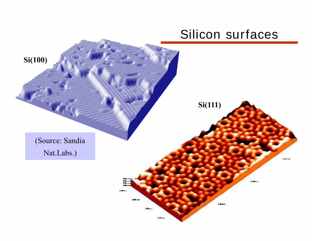
http://cst-www.nrl.navy.mil/lattice/
ZnOCdSCdSeGaNAlN
wurtzite

Structural phase transitions
GaAs, ZincblendeGaAs, Wurtzite
3C - SiC
SiC has about 100 polytypes
4H - SiC 6H - SiC

Electrons
Charge = -1.6022 x 10⁻¹⁹ CMass = 9.11 x 10⁻³¹ kgRadius = ?
0.15 nm

Everything moves like a wave but exchanges energy and momentum like a particle.
Quantum Mechanics
ww
w.alm
aden.ibm.com
/vis/stm/atom
o.html

Everything moves like a wave but exchanges energy and momentum like a particle.

Fluorescent lamp

Molecular energy levels

Semiconductors
valence band conduction bandband gap
molecular orbitals are plane waves

wave vector k
p k
2k
A k-vector points in the direction a wave is propagating.
wavelength:
momentum:
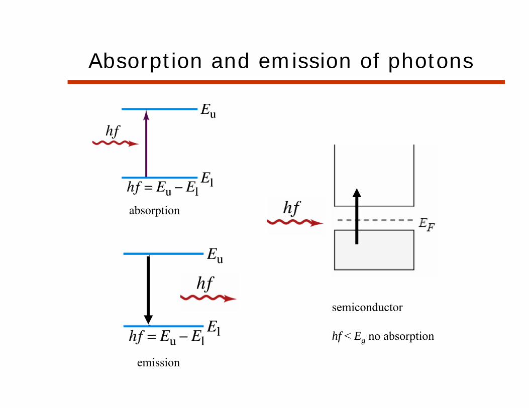
Absorption and emission of photons
semiconductor
hf < Eg no absorption
absorption
emission
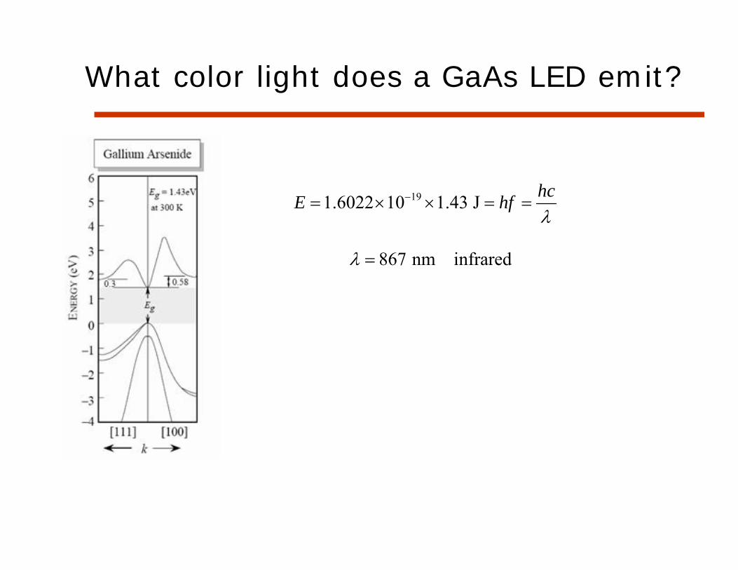
What color light does a GaAs LED emit?
191.6022 10 1.43 J hcE hf
867 nm infrared

direct bandgap:k = 0
photons can be emitted
indirect bandgap:k = 0
phonons are emitted
Direct and indirect band gaps
Momentum must be conserved when photons are absorbed or emitted.
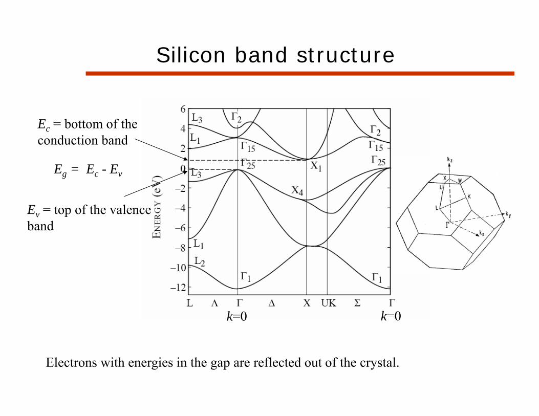
Silicon band structure
k=0
Ec = bottom of the conduction band
Ev = top of the valence band
Eg = Ec - Ev
k=0
Electrons with energies in the gap are reflected out of the crystal.

Light emitting diodes
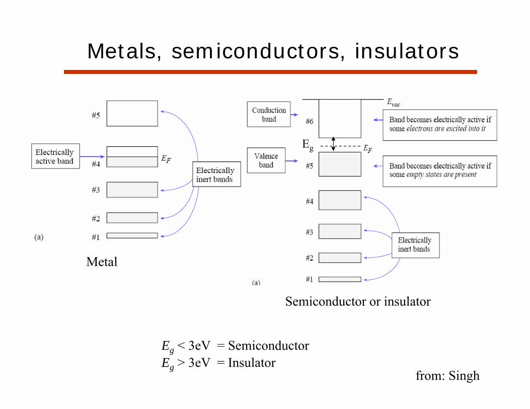
Metals, semiconductors, insulators
Metal
Semiconductor or insulator
Eg < 3eV = SemiconductorEg > 3eV = Insulator
Eg
from: Singh

Copper dispersion relation and density of states
from Ibach & Lueth
4
4
3

from Ibach & Lueth
Germanium
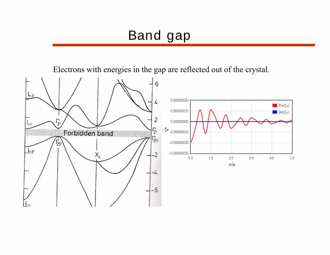
Band gap
Electrons with energies in the gap are reflected out of the crystal.

Density of states
Silicon
filled states empty states
Aluminum
filled states empty states
D(E)
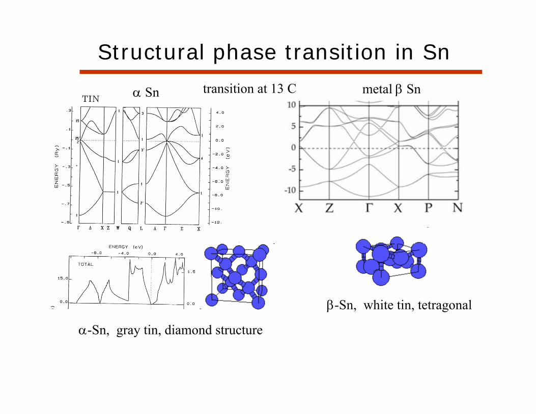
metal Sn Sn
Structural phase transition in Sn
-Sn, gray tin, diamond structure
-Sn, white tin, tetragonal
transition at 13 C

Structural phase transitions
Si, diamond structure
Si II, -Sn, tetragonal
silicon makes a diamond to -Sn transition under pressure

Fermi function
1( )1 exp F
B
f EE E
k T
f(E) is the probability that a state at energy E is occupied.

Silicon density of states
T = 300 K
1012
electrons in the conduction band
T = 300 K