16-Bit Microcontrollers with Large, Dual Partition Flash ...€¦ · • On-Chip USB Transceiver...
468
2015-2017 Microchip Technology Inc. DS30010074E-page 1 PIC24FJ1024GA610/GB610 FAMILY High-Performance CPU • Modified Harvard Architecture • Largest Program Memory Available for PIC24 (1024 Kbytes) for the Most Complex Applications • 32 Kbytes SRAM for All Part Variants • Up to 16 MIPS Operation @ 32 MHz • 8 MHz Fast RC Internal Oscillator: - 96 MHz PLL option - Multiple clock divide options - Run-time self-calibration capability for maintaining better than ±0.20% accuracy - Fast start-up • 17-Bit x 17-Bit Single-Cycle Hardware Fractional/Integer Multiplier • 32-Bit by 16-Bit Hardware Divider • 16-Bit x 16-Bit Working Register Array • C Compiler Optimized Instruction Set Architecture • Two Address Generation Units for Separate Read and Write Addressing of Data Memory Universal Serial Bus Features • USB v2.0 On-The-Go (OTG) Compliant • Dual Role Capable – Can Act as Either Host or Peripheral • Low-Speed (1.5 Mb/s) and Full-Speed (12 Mb/s) USB Operation in Host mode • Full-Speed USB Operation in Device mode • High-Precision PLL for USB • USB Device mode Operation from FRC Oscillator – No Crystal Oscillator Required • Supports up to 32 Endpoints (16 bidirectional): - USB module can use any RAM location on the device as USB endpoint buffers • On-Chip USB Transceiver with Interface for Off-Chip USB Transceiver • Supports Control, Interrupt, Isochronous and Bulk Transfers • On-Chip Pull-up and Pull-Down Resistors Analog Features • 10/12-Bit, up to 24-Channel Analog-to-Digital (A/D) Converter: - 12-bit conversion rate of 200 ksps - Auto-scan and threshold compare features - Conversion available during Sleep • Three Rail-to-Rail, Enhanced Analog Comparators with Programmable Input/Output Configuration • Charge Time Measurement Unit (CTMU): - Used for capacitive touch sensing, up to 24 channels - Time measurement down to 100 ps resolution Low-Power Features • Sleep and Idle modes Selectively Shut Down Peripherals and/or Core for Substantial Power Reduction and Fast Wake-up • Doze mode Allows CPU to Run at a Lower Clock Speed than Peripherals • Alternate Clock modes Allow On-the-Fly Switching to a Lower Clock Speed for Selective Power Reduction • Wide Range Digitally Controlled Oscillator (DCO) for Fast Start-up and Low-Power Operation Special Microcontroller Features • Large, Dual Partition Flash Program Array: - Capable of holding two independent software applications, including bootloader - Permits simultaneous programming of one partition while executing application code from the other - Allows run-time switching between Active Partitions • 10,000 Erase/Write Cycle Endurance, Typical • Data Retention: 20 Years Minimum • Self-Programmable under Software Control • Supply Voltage Range of 2.0V to 3.6V • Operating Ambient Temperature Range of -40°C to +85°C • On-Chip Voltage Regulators (1.8V) for Low-Power Operation • Programmable Reference Clock Output • In-Circuit Serial Programming™ (ICSP™) and In-Circuit Emulation (ICE) via 2 Pins • JTAG Boundary Scan Support • Fail-Safe Clock Monitor Operation: - Detects clock failure and switches to on-chip, low-power RC Oscillator • Power-on Reset (POR), Brown-out Reset (BOR), Power-up Timer (PWRT) and Oscillator Start-up Timer (OST) • Programmable High/Low-Voltage Detect (HLVD) • Flexible Watchdog Timer (WDT) with its Own RC Oscillator for Reliable Operation 16-Bit Microcontrollers with Large, Dual Partition Flash Program Memory and USB On-The-Go (OTG)
Transcript of 16-Bit Microcontrollers with Large, Dual Partition Flash ...€¦ · • On-Chip USB Transceiver...
PIC24FJ1024GA610/GB610 FAMILY
16-Bit Microcontrollers with Large, Dual Partition Flash Program Memory and USB On-The-Go (OTG)
High-Performance CPU
• Modified Harvard Architecture• Largest Program Memory Available for PIC24
(1024 Kbytes) for the Most Complex Applications• 32 Kbytes SRAM for All Part Variants• Up to 16 MIPS Operation @ 32 MHz • 8 MHz Fast RC Internal Oscillator:
- 96 MHz PLL option- Multiple clock divide options- Run-time self-calibration capability for maintaining
better than ±0.20% accuracy- Fast start-up
• 17-Bit x 17-Bit Single-Cycle Hardware Fractional/Integer Multiplier
• 32-Bit by 16-Bit Hardware Divider• 16-Bit x 16-Bit Working Register Array• C Compiler Optimized Instruction Set Architecture• Two Address Generation Units for Separate Read
and Write Addressing of Data Memory
Universal Serial Bus Features
• USB v2.0 On-The-Go (OTG) Compliant• Dual Role Capable – Can Act as Either Host or Peripheral• Low-Speed (1.5 Mb/s) and Full-Speed (12 Mb/s)
USB Operation in Host mode• Full-Speed USB Operation in Device mode• High-Precision PLL for USB• USB Device mode Operation from FRC Oscillator –
No Crystal Oscillator Required• Supports up to 32 Endpoints (16 bidirectional):
- USB module can use any RAM location on the device as USB endpoint buffers
• On-Chip USB Transceiver with Interface for Off-Chip USB Transceiver
• Supports Control, Interrupt, Isochronous and Bulk Transfers
• On-Chip Pull-up and Pull-Down Resistors
Analog Features
• 10/12-Bit, up to 24-Channel Analog-to-Digital (A/D) Converter:- 12-bit conversion rate of 200 ksps- Auto-scan and threshold compare features- Conversion available during Sleep
• Three Rail-to-Rail, Enhanced Analog Comparators with Programmable Input/Output Configuration
• Charge Time Measurement Unit (CTMU):- Used for capacitive touch sensing, up to 24 channels- Time measurement down to 100 ps resolution
Low-Power Features
• Sleep and Idle modes Selectively Shut Down Peripherals and/or Core for Substantial Power Reduction and Fast Wake-up
• Doze mode Allows CPU to Run at a Lower Clock Speed than Peripherals
• Alternate Clock modes Allow On-the-Fly Switching to a Lower Clock Speed for Selective Power Reduction
• Wide Range Digitally Controlled Oscillator (DCO) for Fast Start-up and Low-Power Operation
Special Microcontroller Features
• Large, Dual Partition Flash Program Array:- Capable of holding two independent software
applications, including bootloader- Permits simultaneous programming of one partition
while executing application code from the other- Allows run-time switching between
Active Partitions• 10,000 Erase/Write Cycle Endurance, Typical• Data Retention: 20 Years Minimum• Self-Programmable under Software Control• Supply Voltage Range of 2.0V to 3.6V• Operating Ambient Temperature Range of
-40°C to +85°C• On-Chip Voltage Regulators (1.8V) for Low-Power
Operation• Programmable Reference Clock Output• In-Circuit Serial Programming™ (ICSP™) and
In-Circuit Emulation (ICE) via 2 Pins• JTAG Boundary Scan Support • Fail-Safe Clock Monitor Operation:
- Detects clock failure and switches to on-chip, low-power RC Oscillator
• Power-on Reset (POR), Brown-out Reset (BOR), Power-up Timer (PWRT) and Oscillator Start-up Timer (OST)
• Programmable High/Low-Voltage Detect (HLVD)• Flexible Watchdog Timer (WDT) with its Own
RC Oscillator for Reliable Operation
2015-2017 Microchip Technology Inc. DS30010074E-page 1

PIC24FJ1024GA610/GB610 FAMILY
Peripheral Features
• Peripheral Pin Select (PPS) –Allows Independent I/O Mapping of Many Peripherals
• Up to 5 External Interrupt Sources• Configurable Interrupt-on-Change on All I/O Pins:
- Each pin is independently configurable for rising edge or falling edge change detection
• Eight-Channel DMA Supports All Peripheral modules:- Minimizes CPU overhead and increases data
throughput• Five 16-Bit Timers/Counters with Prescalers:
- Can be paired as 32-bit timers/counters• Six Input Capture modules, Each with a Dedicated
16-Bit Timer• Six Output Compare/PWM modules, Each with a
Dedicated 16-Bit Timer• Four Single Output CCPs (SCCPs) and Three
Multiple Output CCPs (MCCPs):- Independent 16/32-bit time base for each module- Internal time base and period registers- Legacy PIC24F Capture and Compare modes
(16 and 32-bit)- Special Variable Frequency Pulse and Brushless
DC Motor Output modes
• Enhanced Parallel Master/Slave Port (EPMP/EPSP)• Hardware Real-Time Clock/Calendar (RTCC) with
Timestamping• Three 3-Wire/4-Wire SPI modules:
- Support 4 Frame modes - 8-level FIFO buffer- Support I2S operation
• Three I2C modules Support Multi-Master/Slave mode and 7-Bit/10-Bit Addressing
• Six UART modules:- Support RS-485, RS-232 and LIN/J2602- On-chip hardware encoder/decoder for IrDA®
- Auto-wake-up on Auto-Baud Detect (ABD)- 4-level deep FIFO buffer
• Programmable 32-Bit Cyclic Redundancy Check (CRC) Generator
• Four Configurable Logic Cells (CLCs):- Two inputs and one output, all mappable to
peripherals or I/O pins- AND/OR/XOR logic and D/JK flip-flop functions
• High-Current Sink/Source (18 mA/18 mA) on All I/O Pins• Configurable Open-Drain Outputs on Digital I/O Pins• 5.5V Tolerant Inputs on Multiple I/O Pins
DS30010074E-page 2 2015-2017 Microchip Technology Inc.

PIC24FJ1024GA610/GB610 FAMILY
PIC24FJ1024GA610/GB610 FAMILY PRODUCT FAMILIES
The device names, pin counts, memory sizes andperipheral availability of each device are listed inTable 1. Their pinout diagrams appear on the followingpages.
TABLE 1: PIC24FJ1024GA610/GB610 GENERAL PURPOSE FAMILIES
Device
Memory Pins Analog Digital
RT
CC
US
B O
TG
Pro
gra
m(b
yte
s)
Dat
a(b
yte
s)
Tota
l
I/O
10/1
2-B
it A
/D (
ch
)
Co
mp
ara
tor
CT
MU
1
6/3
2-B
it T
ime
r
IC/O
C/P
WM
MC
CP
/SC
CP
I2C
SP
I
UA
RT
w/I
rDA
®
EP
MP
/EP
SP
CL
C
PIC24FJ128GA606 128K 32K 64 53 16 3 Y 5/2 6/6 3/4 3 3 6/2 Y 4 Y N
PIC24FJ256GA606 256K 32K 64 53 16 3 Y 5/2 6/6 3/4 3 3 6/2 Y 4 Y N
PIC24FJ512GA606 512K 32K 64 53 16 3 Y 5/2 6/6 3/4 3 3 6/2 Y 4 Y N
PIC24FJ1024GA606 1024K 32K 64 53 16 3 Y 5/2 6/6 3/4 3 3 6/2 Y 4 Y N
PIC24FJ128GA610 128K 32K 100 85 24 3 Y 5/2 6/6 3/4 3 3 6/2 Y 4 Y N
PIC24FJ256GA610 256K 32K 100 85 24 3 Y 5/2 6/6 3/4 3 3 6/2 Y 4 Y N
PIC24FJ512GA610 512K 32K 100 85 24 3 Y 5/2 6/6 3/4 3 3 6/2 Y 4 Y N
PIC24FJ1024GA610 1024K 32K 100 85 24 3 Y 5/2 6/6 3/4 3 3 6/2 Y 4 Y N
PIC24FJ128GB606 128K 32K 64 53 16 3 Y 5/2 6/6 3/4 3 3 6/2 Y 4 Y Y
PIC24FJ256GB606 256K 32K 64 53 16 3 Y 5/2 6/6 3/4 3 3 6/2 Y 4 Y Y
PIC24FJ512GB606 512K 32K 64 53 16 3 Y 5/2 6/6 3/4 3 3 6/2 Y 4 Y Y
PIC24FJ1024GB606 1024K 32K 64 53 16 3 Y 5/2 6/6 3/4 3 3 6/2 Y 4 Y Y
PIC24FJ128GB610 128K 32K 100 85 24 3 Y 5/2 6/6 3/4 3 3 6/2 Y 4 Y Y
PIC24FJ256GB610 256K 32K 100 85 24 3 Y 5/2 6/6 3/4 3 3 6/2 Y 4 Y Y
PIC24FJ512GB610 512K 32K 100 85 24 3 Y 5/2 6/6 3/4 3 3 6/2 Y 4 Y Y
PIC24FJ1024GB610 1024K 32K 100 85 24 3 Y 5/2 6/6 3/4 3 3 6/2 Y 4 Y Y
2015-2017 Microchip Technology Inc. DS30010074E-page 3
PIC24FJ1024GA610/GB610 FAMILY
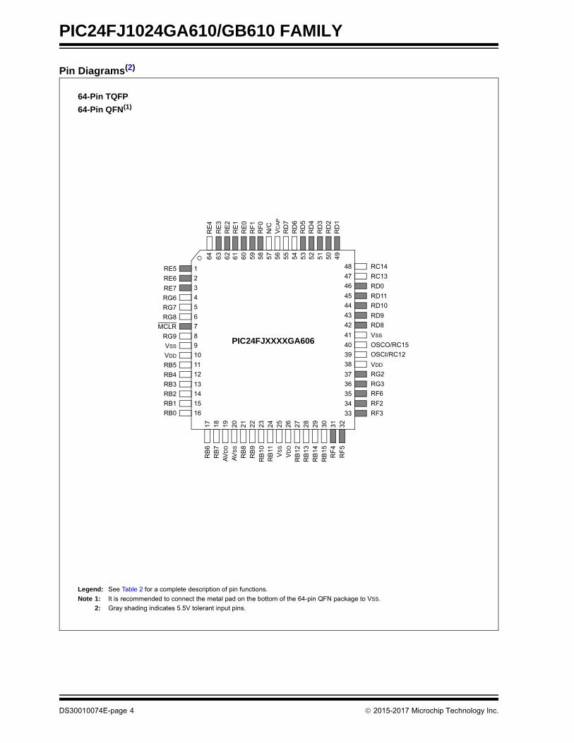
Pin Diagrams(2)
Legend: See Table 2 for a complete description of pin functions.
Note 1: It is recommended to connect the metal pad on the bottom of the 64-pin QFN package to VSS.
2: Gray shading indicates 5.5V tolerant input pins.
64-Pin TQFP
64-Pin QFN(1)
2
3
4
5
6
7
8
9
10
11
12
13
14
15
16
48
47
22
44
24 25 26 27 28 29 30 31 32
1
46
45
23
43
42
41
40
39
63
62
61
59
60
58
57
56
54
55
53
52
51
49
50
38
37
34
36
35
33
17 19 20 21186
4
VDD
VSS
RG9
MCLR
RG8
RG7
RG6
RE7
RE6
RE5
RB5
RB4
RB3
RB2
RB1
RB0
OSCI/RC12
OSCO/RC15
VSS
RD8
RD9
RD10
RD11
RD0
RC13
RC14
VDD
RG2
RG3
RF6
RF2
RF3
VD
D
VS
S
RB
11R
B10
RB
9R
B8
AV
SS
AV
DD
RB
7R
B6
RB
12R
B13
RB
14R
B15
RF
4
RF
5
RD
7V
CA
P
N/C
RF
0R
F1
RE
0R
E1
RE
2R
E3
RE
4
RD
6R
D5
RD
4R
D3
RD
2R
D1
PIC24FJXXXXGA606
DS30010074E-page 4 2015-2017 Microchip Technology Inc.

PIC24FJ1024GA610/GB610 FAMILY
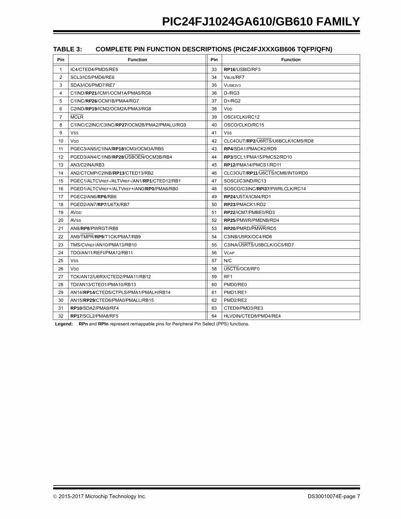
TABLE 2: COMPLETE PIN FUNCTION DESCRIPTIONS (PIC24FJXXXGA606 TQFP/QFN)
Pin Function Pin Function
1 IC4/CTED4/PMD5/RE5 33 RP16/RF3
2 SCL3/IC5/PMD6/RE6 34 RP30/RF2
3 SDA3/IC6/PMD7/RE7 35 INT0/RF6
4 C1IND/RP21/ICM1/OCM1A/PMA5/RG6 36 SDA1/RG3
5 C1INC/RP26/OCM1B/PMA4/RG7 37 SCL1/RG2
6 C2IND/RP19/ICM2/OCM2A/PMA3/RG8 38 VDD
7 MCLR 39 OSCI/CLKI/RC12
8 C1INC/C2INC/C3INC/RP27/OCM2B/PMA2/PMALU/RG9 40 OSCO/CLKO/RC15
9 VSS 41 VSS
10 VDD 42 CLC4OUT/RP2/U6RTS/U6BCLK/ICM5/RD8
11 PGEC3/AN5/C1INA/RP18/ICM3/OCM3A/RB5 43 RP4/PMACK2/RD9
12 PGED3/AN4/C1INB/RP28/OCM3B/RB4 44 RP3/PMA15/PMCS2/RD10
13 AN3/C2INA/RB3 45 RP12/PMA14/PMCS1/RD11
14 AN2/CTCMP/C2INB/RP13/CTED13/RB2 46 CLC3OUT/RP11/U6CTS/ICM6/RD0
15 PGEC1/ALTCVREF-/ALTVREF-/AN1/RP1/CTED12/RB1 47 SOSCI/C3IND/RC13
16 PGED1/ALTCVREF+/ALTVREF+/AN0/RP0/PMA6/RB0 48 SOSCO/C3INC/RPI37/PWRLCLK/RC14
17 PGEC2/AN6/RP6/RB6 49 RP24/U5TX/ICM4/RD1
18 PGED2/AN7/RP7/U6TX/RB7 50 RP23/PMACK1/RD2
19 AVDD 51 RP22/ICM7/PMBE0/RD3
20 AVSS 52 RP25/PMWR/PMENB/RD4
21 AN8/RP8/PWRGT/RB8 53 RP20/PMRD/PMWR/RD5
22 AN9/TMPR/RP9/T1CK/PMA7/RB9 54 C3INB/U5RX/OC4/RD6
23 TMS/CVREF/AN10/PMA13/RB10 55 C3INA/U5RTS/U5BCLK/OC5/RD7
24 TDO/AN11/REFI/PMA12/RB11 56 VCAP
25 VSS 57 N/C
26 VDD 58 U5CTS/OC6/RF0
27 TCK/AN12/U6RX/CTED2/PMA11/RB12 59 RF1
28 TDI/AN13/CTED1/PMA10/RB13 60 PMD0/RE0
29 AN14/RP14/CTED5/CTPLS/PMA1/PMALH/RB14 61 PMD1/RE1
30 AN15/RP29/CTED6/PMA0/PMALL/RB15 62 PMD2/RE2
31 RP10/SDA2/PMA9/RF4 63 CTED9/PMD3/RE3
32 RP17/SCL2/PMA8/RF5 64 HLVDIN/CTED8/PMD4/RE4
Legend: RPn and RPIn represent remappable pins for Peripheral Pin Select (PPS) functions.
2015-2017 Microchip Technology Inc. DS30010074E-page 5

PIC24FJ1024GA610/GB610 FAMILY
Pin Diagrams(2) (Continued)
Legend: See Table 3 for a complete description of pin functions.
Note 1: It is recommended to connect the metal pad on the bottom of the 64-pin QFN package to VSS.
2: Gray shading indicates 5.5V tolerant input pins.
64-Pin TQFP
64-Pin QFN(1)
2
3
4
5
6
7
8
9
10
11
12
13
14
15
16
48
47
22
44
24 25 26 27 28 29 30 31 32
1
46
45
23
43
42
41
40
39
63 62 61 5960 58 57 56 5455 53 52 51 4950
38
37
34
36
35
33
17 19 20 211864
VDD
VSS
RG9
MCLR
RG8
RG7
RG6
RE7
RE6
RE5
RB5
RB4
RB3
RB2
RB1
RB0
OSCI/RC12
OSCO/RC15
VSS
RD8
RD9
RD10
RD11
RD0
RC13
RC14
VDD
D+/RG2
D-/RG3
VUSB3V3
VBUS/RF7
RF3
VD
D
VS
S
RB
11R
B10
RB
9R
B8
AV
SS
AV
DD
RB
7R
B6
RB
12R
B13
RB
14R
B15
RF
4
RF
5
RD
7V
CA
P
N/C
RF
0R
F1
RE
0R
E1
RE
2R
E3
RE
4
RD
6R
D5
RD
4R
D3
RD
2R
D1
PIC24FJXXXXGB606
15
DS30010074E-page 6 2015-2017 Microchip Technology Inc.
PIC24FJ1024GA610/GB610 FAMILY
TABLE 3: COMPLETE PIN FUNCTION DESCRIPTIONS (PIC24FJXXXGB606 TQFP/QFN)
Pin Function Pin Function
1 IC4/CTED4/PMD5/RE5 33 RP16/USBID/RF3
2 SCL3/IC5/PMD6/RE6 34 VBUS/RF7
3 SDA3/IC6/PMD7/RE7 35 VUSB3V3
4 C1IND/RP21/ICM1/OCM1A/PMA5/RG6 36 D-/RG3
5 C1INC/RP26/OCM1B/PMA4/RG7 37 D+/RG2
6 C2IND/RP19/ICM2/OCM2A/PMA3/RG8 38 VDD
7 MCLR 39 OSCI/CLKI/RC12
8 C1INC/C2INC/C3INC/RP27/OCM2B/PMA2/PMALU/RG9 40 OSCO/CLKO/RC15
9 VSS 41 VSS
10 VDD 42 CLC4OUT/RP2/U6RTS/U6BCLK/ICM5/RD8
11 PGEC3/AN5/C1INA/RP18/ICM3/OCM3A/RB5 43 RP4/SDA1/PMACK2/RD9
12 PGED3/AN4/C1INB/RP28/USBOEN/OCM3B/RB4 44 RP3/SCL1/PMA15/PMCS2/RD10
13 AN3/C2INA/RB3 45 RP12/PMA14/PMCS1/RD11
14 AN2/CTCMP/C2INB/RP13/CTED13/RB2 46 CLC3OUT/RP11/U6CTS/ICM6/INT0/RD0
15 PGEC1/ALTCVREF-/ALTVREF-/AN1/RP1/CTED12/RB1 47 SOSCI/C3IND/RC13
16 PGED1/ALTCVREF+/ALTVREF+/AN0/RP0/PMA6/RB0 48 SOSCO/C3INC/RPI37/PWRLCLK/RC14
17 PGEC2/AN6/RP6/RB6 49 RP24/U5TX/ICM4/RD1
18 PGED2/AN7/RP7/U6TX/RB7 50 RP23/PMACK1/RD2
19 AVDD 51 RP22/ICM7/PMBE0/RD3
20 AVSS 52 RP25/PMWR/PMENB/RD4
21 AN8/RP8/PWRGT/RB8 53 RP20/PMRD/PMWR/RD5
22 AN9/TMPR/RP9/T1CK/PMA7/RB9 54 C3INB/U5RX/OC4/RD6
23 TMS/CVREF/AN10/PMA13/RB10 55 C3INA/U5RTS/U5BCLK/OC5/RD7
24 TDO/AN11/REFI/PMA12/RB11 56 VCAP
25 VSS 57 N/C
26 VDD 58 U5CTS/OC6/RF0
27 TCK/AN12/U6RX/CTED2/PMA11/RB12 59 RF1
28 TDI/AN13/CTED1/PMA10/RB13 60 PMD0/RE0
29 AN14/RP14/CTED5/CTPLS/PMA1/PMALH/RB14 61 PMD1/RE1
30 AN15/RP29/CTED6/PMA0/PMALL/RB15 62 PMD2/RE2
31 RP10/SDA2/PMA9/RF4 63 CTED9/PMD3/RE3
32 RP17/SCL2/PMA8/RF5 64 HLVDIN/CTED8/PMD4/RE4
Legend: RPn and RPIn represent remappable pins for Peripheral Pin Select (PPS) functions.
2015-2017 Microchip Technology Inc. DS30010074E-page 7
PIC24FJ1024GA610/GB610 FAMILY
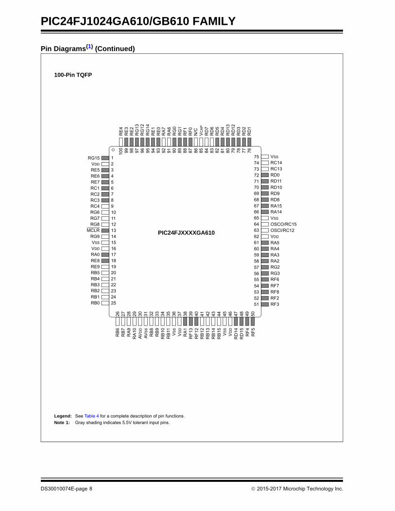
Pin Diagrams(1) (Continued)
Legend: See Table 4 for a complete description of pin functions.
Note 1: Gray shading indicates 5.5V tolerant input pins.
100-Pin TQFP
9294 93 91 90 89 88 87 86 85 84 83 82 81 80 79 78
20
2345678910111213141516
65646362616059
26
56
4544434241403928 29 30 31 32 33 34 35 36 37 38
171819
2122
95
1
7677
72717069
686766
757473
58
57
2423
25
9698 979927 46 47 48 49 50
55
54535251
100
RD
5R
D4
RD
13R
D12
RD
3R
D2
RD
1
RA
7R
A6
RE
2R
G13
RG
12R
G14
RE
1R
E0
RG
0
RE
4R
E3
RF
0
VC
AP
RC13RD0
RD10RD9RD8
RD11
RA15RA14
OSCO/RC15OSCI/RC12VDD
RG2
RF6
RF7RF8
RG3
RF2RF3
VSS
RC14
RA
10R
A9
AV
DD
AV
SS
RB
8R
B9
RB
10R
B11
VD
D
RF
12R
F13
VS
S
VD
D
RD
15R
D14
RB
6R
B7
RF
5R
F4
RE5RE6RE7RC1RC2RC3RC4RG6
VDD
RA0RE8RE9RB5RB4RB3RB2
RG7RG8
RB1RB0
RG15VDD
RG9MCLR
RB
12R
B13
RB
14R
B15
RG
1R
F1
RD
7R
D6
RA5
RA3RA2
VSS
VS
S
VSS
N/C
RA4
RA
1
PIC24FJXXXXGA610
DS30010074E-page 8 2015-2017 Microchip Technology Inc.

PIC24FJ1024GA610/GB610 FAMILY
TABLE 4: COMPLETE PIN FUNCTION DESCRIPTIONS (PIC24FJXXXGA610 TQFP)
Pin Function Pin Function
1 OCM1C/CTED3/RG15 51 RP16/RF3
2 VDD 52 RP30/RF2
3 IC4/CTED4/PMD5/RE5 53 RP15/RF8
4 SCL3/IC5/PMD6/RE6 54 RF7
5 SDA3/IC6/PMD7/RE7 55 INT0/RF6
6 RPI38/OCM1D/RC1 56 SDA1/RG3
7 RPI39/OCM2C/RC2 57 SCL1/RG2
8 RPI40/OCM2D/RC3 58 PMPCS1/SCL2/RA2
9 AN16/RPI41/OCM3C/PMCS2/RC4 59 SDA2/PMA20/RA3
10 AN17/C1IND/RP21/ICM1/OCM1A/PMA5/RG6 60 TDI/PMA21/RA4
11 AN18/C1INC/RP26/OCM1B/PMA4/RG7 61 TDO/RA5
12 AN19/C2IND/RP19/ICM2/OCM2A/PMA3/RG8 62 VDD
13 MCLR 63 OSCI/CLKI/RC12
14 AN20/C1INC/C2INC/C3INC/RP27/OCM2B/PMA2/PMALU/RG9 64 OSCO/CLKO/RC15
15 VSS 65 VSS
16 VDD 66 RPI36/PMA22/RA14
17 TMS/OCM3D/RA0 67 RPI35/PMBE1/RA15
18 RPI33/PMCS1/RE8 68 CLC4OUT/RP2/U6RTS/U6BCLK/ICM5/RD8
19 AN21/RPI34/PMA19/RE9 69 RP4/PMACK2/RD9
20 PGEC3/AN5/C1INA/RP18/ICM3/OCM3A/RB5 70 RP3/PMA15/PMCS2/RD10
21 PGED3/AN4/C1INB/RP28/OCM3B/RB4 71 RP12/PMA14/PMCS1/RD11
22 AN3/C2INA/RB3 72 CLC3OUT/RP11/U6CTS/ICM6/RD0
23 AN2/CTCMP/C2INB/RP13/CTED13/RB2 73 SOSCI/C3IND/RC13
24 PGEC1/ALTCVREF-/ALTVREF-/AN1/RP1/CTED12/RB1 74 SOSCO/C3INC/RPI37/PWRLCLK/RC14
25 PGED1/ALTCVREF+/ALTVREF+/AN0/RP0/RB0 75 VSS
26 PGEC2/AN6/RP6/RB6 76 RP24/U5TX/ICM4/RD1
27 PGED2/AN7/RP7/U6TX/RB7 77 RP23/PMACK1/RD2
28 CVREF-/VREF-/PMA7/RA9 78 RP22/ICM7/PMBE0/RD3
29 CVREF+/VREF+/PMA6/RA10 79 RPI42/OCM3E/PMD12/RD12
30 AVDD 80 OCM3F/PMD13/RD13
31 AVSS 81 RP25/PMWR/PMENB/RD4
32 AN8/RP8/PWRGT/RB8 82 RP20/PMRD/PMWR/RD5
33 AN9/TMPR/RP9/T1CK/RB9 83 C3INB/U5RX/OC4/PMD14/RD6
34 CVREF/AN10/PMA13/RB10 84 C3INA/U5RTS/U5BCLK/OC5/PMD15/RD7
35 AN11/REFI/PMA12/RB11 85 VCAP
36 VSS 86 N/C
37 VDD 87 U5CTS/OC6/PMD11/RF0
38 TCK/RA1 88 PMD10/RF1
39 RP31/RF13 89 PMD9/RG1
40 RPI32/CTED7/PMA18/RF12 90 PMD8/RG0
41 AN12/U6RX/CTED2/PMA11/RB12 91 AN23/OCM1E/RA6
42 AN13/CTED1/PMA10/RB13 92 AN22/OCM1F/PMA17/RA7
43 AN14/RP14/CTED5/CTPLS/PMA1/PMALH/RB14 93 PMD0/RE0
44 AN15/RP29/CTED6/PMA0/PMALL/RB15 94 PMD1/RE1
45 VSS 95 CTED11/PMA16/RG14
46 VDD 96 OCM2E/RG12
47 RPI43/RD14 97 OCM2F/CTED10/RG13
48 RP5/RD15 98 PMD2/RE2
49 RP10/PMA9/RF4 99 CTED9/PMD3/RE3
50 RP17/PMA8/RF5 100 HLVDIN/CTED8/PMD4/RE4
Legend: RPn and RPIn represent remappable pins for Peripheral Pin Select (PPS) functions.
2015-2017 Microchip Technology Inc. DS30010074E-page 9

PIC24FJ1024GA610/GB610 FAMILY
Pin Diagrams(1) (Continued)
Legend: See Table 5 for a complete description of pin functions.
Note 1: Gray shading indicates 5.5V tolerant input pins.
100-Pin TQFP
9294 93 91 90 89 88 87 86 85 84 83 82 81 80 79 78
20
234567
8910111213141516
65646362616059
26
56
4544434241403928 29 30 31 32 33 34 35 36 37 38
171819
2122
95
1
7677
72
717069686766
75
7473
5857
2423
25
9698 979927 46 47 48 49 50
55
545352
51
100
RD
5R
D4
RD
13R
D12
RD
3R
D2
RD
1
RA
7R
A6
RE
2R
G13
RG
12R
G14
RE
1R
E0
RG
0
RE
4R
E3
RF
0
VC
AP
RC13RD0
RD10RD9RD8
RD11
RA15RA14
OSCO/RC15OSCI/RC12VDD
D+/RG2
VUSB3V3
VBUS/RF7RF8
D-/RG3
RF2RF3
VSS
RC14
RA
10R
A9
AV
DD
AV
SS
RB
8R
B9
RB
10R
B11
VD
D
RF
12R
F13
VS
S
VD
D
RD
15R
D14
RB
6R
B7
RF
5R
F4
RE5RE6RE7RC1RC2RC3RC4RG6
VDD
RA0RE8RE9RB5RB4RB3RB2
RG7RG8
RB1RB0
RG15VDD
RG9MCLR
RB
12R
B13
RB
14R
B15
RG
1R
F1
RD
7R
D6
RA5
RA3RA2
VSS
VS
S
VSS
N/C
RA4
RA
1
PIC24FJXXXXGB610
DS30010074E-page 10 2015-2017 Microchip Technology Inc.

PIC24FJ1024GA610/GB610 FAMILY
TABLE 5: COMPLETE PIN FUNCTION DESCRIPTIONS (PIC24FJXXXGB610 TQFP)
Pin Function Pin Function
1 OCM1C/CTED3/RG15 51 RP16/USBID/RF3
2 VDD 52 RP30/RF2
3 IC4/CTED4/PMD5/RE5 53 RP15/RF8
4 SCL3/IC5/PMD6/RE6 54 VBUS/RF7
5 SDA3/IC6/PMD7/RE7 55 VUSB3V3
6 RPI38/OCM1D/RC1 56 D-/RG3
7 RPI39/OCM2C/RC2 57 D+/RG2
8 RPI40/OCM2D/RC3 58 PMPCS1/SCL2/RA2
9 AN16/RPI41/OCM3C/PMCS2/RC4 59 SDA2/PMA20/RA3
10 AN17/C1IND/RP21/ICM1/OCM1A/PMA5/RG6 60 TDI/PMA21/RA4
11 AN18/C1INC/RP26/OCM1B/PMA4/RG7 61 TDO/RA5
12 AN19/C2IND/RP19/ICM2/OCM2A/PMA3/RG8 62 VDD
13 MCLR 63 OSCI/CLKI/RC12
14 AN20/C1INC/C2INC/C3INC/RP27/OCM2B/PMA2/PMALU/RG9 64 OSCO/CLKO/RC15
15 VSS 65 VSS
16 VDD 66 RPI36/SCL1/PMA22/RA14
17 TMS/OCM3D/RA0 67 RPI35/SDA1/PMBE1/RA15
18 RPI33/PMCS1/RE8 68 CLC4OUT/RP2/U6RTS/U6BCLK/ICM5/RD8
19 AN21/RPI34/PMA19/RE9 69 RP4/PMACK2/RD9
20 PGEC3/AN5/C1INA/RP18/ICM3/OCM3A/RB5 70 RP3/PMA15/PMCS2/RD10
21 PGED3/AN4/C1INB/RP28/USBOEN/OCM3B/RB4 71 RP12/PMA14/PMCS1/RD11
22 AN3/C2INA/RB3 72 CLC3OUT/RP11/U6CTS/ICM6/INT0/RD0
23 AN2/CTCMP/C2INB/RP13/CTED13/RB2 73 SOSCI/C3IND/RC13
24 PGEC1/ALTCVREF-/ALTVREF-/AN1/RP1/CTED12/RB1 74 SOSCO/C3INC/RPI37/PWRLCLK/RC14
25 PGED1/ALTCVREF+/ALTVREF+/AN0/RP0/RB0 75 VSS
26 PGEC2/AN6/RP6/RB6 76 RP24/U5TX/ICM4/RD1
27 PGED2/AN7/RP7/U6TX/RB7 77 RP23/PMACK1/RD2
28 CVREF-/VREF-/PMA7/RA9 78 RP22/ICM7/PMBE0/RD3
29 CVREF+/VREF+/PMA6/RA10 79 RPI42/OCM3E/PMD12/RD12
30 AVDD 80 OCM3F/PMD13/RD13
31 AVSS 81 RP25/PMWR/PMENB/RD4
32 AN8/RP8/PWRGT/RB8 82 RP20/PMRD/PMWR/RD5
33 AN9/TMPR/RP9/T1CK/RB9 83 C3INB/U5RX/OC4/PMD14/RD6
34 CVREF/AN10/PMA13/RB10 84 C3INA/U5RTS/U5BCLK/OC5/PMD15/RD7
35 AN11/REFI/PMA12/RB11 85 VCAP
36 VSS 86 N/C
37 VDD 87 U5CTS/OC6/PMD11/RF0
38 TCK/RA1 88 PMD10/RF1
39 RP31/RF13 89 PMD9/RG1
40 RPI32/CTED7/PMA18/RF12 90 PMD8/RG0
41 AN12/U6RX/CTED2/PMA11/RB12 91 AN23/OCM1E/RA6
42 AN13/CTED1/PMA10/RB13 92 AN22/OCM1F/PMA17/RA7
43 AN14/RP14/CTED5/CTPLS/PMA1/PMALH/RB14 93 PMD0/RE0
44 AN15/RP29/CTED6/PMA0/PMALL/RB15 94 PMD1/RE1
45 VSS 95 CTED11/PMA16/RG14
46 VDD 96 OCM2E/RG12
47 RPI43/RD14 97 OCM2F/CTED10/RG13
48 RP5/RD15 98 PMD2/RE2
49 RP10/PMA9/RF4 99 CTED9/PMD3/RE3
50 RP17/PMA8/RF5 100 HLVDIN/CTED8/PMD4/RE4
Legend: RPn and RPIn represent remappable pins for Peripheral Pin Select (PPS) functions.
2015-2017 Microchip Technology Inc. DS30010074E-page 11

PIC24FJ1024GA610/GB610 FAMILY
Pin Diagrams(1) (Continued)
Legend: See Table 6 for a complete description of pin functions.
Note 1: Gray shading indicates 5.5V tolerant input pins.
PIC24FJXXXGA610 121-Pin BGA
RE4 RE3 RG13 RE0 RG0 RF1 RD12 RD2 RD1
RG15 RE2 RE1 RA7 RF0 VCAP RD5 RD3 VSS RC14
RE6 VDD RG12 RG14 RA6 RD7 RD4 RC13 RD11
RC1 RE7 RE5 RD6 RD13 RD0 RD10
RC4 RC3 RG6 RC2 RG1 RA15 RD8 RD9 RA14
MCLR RG8 RG9 RG7 VSS VDD RC12 VSS RC15
RE8 RE9 RA0 VDD VSS VSS RA5 RA3 RA4
RB5 RB4 VDD RF7 RF6 RG2 RA2
RB3 RB2 RB7 AVDD RB11 RA1 RB12 RF8 RG3
RB1 RB0 RA10 RB8 RF12 RB14 VDD RD15 RF3 RF2
RB6 RA9 AVSS RB9 RB10 RF13 RB13 RB15 RD14 RF4 RF5
1 2 3 4 5 6 7 8 9 10 11
A
B
C
D
E
F
G
H
J
K
L
N/C N/C
N/C
N/C
N/CN/CN/C
N/C N/C
N/C
N/C
N/C N/C
N/C N/C
N/C N/C N/C
N/C N/C
N/C
N/C
DS30010074E-page 12 2015-2017 Microchip Technology Inc.

PIC24FJ1024GA610/GB610 FAMILY
TABLE 6: COMPLETE PIN FUNCTION DESCRIPTIONS (PIC24FJXXXGA610 BGA)
Pin Full Pin Name Pin Full Pin Name
A1 HLVDIN/CTED8/PMD4/RE4 E1 AN16/RPI41/OCM3C/PMCS2/RC4
A2 CTED9/PMD3/RE3 E2 RPI40/OCM2D/RC3
A3 OCM2F/CTED10/RG13 E3 AN17/C1IND/RP21/ICM1/OCM1A/PMA5/RG6
A4 PMD0/RE0 E4 RPI39/OCM2C/RC2
A5 PMD8/RG0 E5 N/C
A6 PMD10/RF1 E6 PMD9/RG1
A7 N/C E7 N/C
A8 N/C E8 RPI35/PMBE1/RA15
A9 RPI42/OCM3E/PMD12/RD12 E9 CLC4OUT/RP2/U6RTS/U6BCLK/ICM5/RD8
A10 RP23/PMACK1/RD2 E10 RP4/PMACK2/RD9
A11 RP24/U5TX/ICM4/RD1 E11 RPI36/PMA22/RA14
B1 N/C F1 MCLR
B2 OCM1C/CTED3/RG15 F2 AN19/C2IND/RP19/ICM2/OCM2A/PMA3/RG8
B3 PMD2/RE2 F3 AN20/C1INC/C2INC/C3INC/RP27/OCM2B/PMA2/PMALU/ RG9
B4 PMD1/RE1 F4 AN18/C1INC/RP26/OCM1B/PMA4/RG7
B5 AN22/OCM1F/PMA17/RA7 F5 VSS
B6 U5CTS/OC6/PMD11/RF0 F6 N/C
B7 VCAP F7 N/C
B8 RP20/PMRD/PMWR/RD5 F8 VDD
B9 RP22/ICM7/PMBE0/RD3 F9 OSCI/CLKI/RC12
B10 VSS F10 VSS
B11 SOSCO/C3INC/RPI37/PWRLCLK/RC14 F11 OSCO/CLKO/RC15
C1 SCL3/IC5/PMD6/RE6 G1 RPI33/PMCS1/RE8
C2 VDD G2 AN21/RPI34/PMA19/RE9
C3 OCM2E/RG12 G3 TMS/OCM3D/RA0
C4 CTED11/PMA16/RG14 G4 N/C
C5 AN23/OCM1E/RA6 G5 VDD
C6 N/C G6 VSS
C7 C3INA/U5RTS/U5BCLK/OC5/PMD15/RD7 G7 VSS
C8 RP25/PMWR/PMENB/RD4 G8 N/C
C9 N/C G9 TDO/RA5
C10 SOSCI/C3IND/RC13 G10 SDA2/PMA20/RA3
C11 RP12/PMA14/PMCS1/RD11 G11 TDI/PMA21/RA4
D1 RPI38/OCM1D/RC1 H1 PGEC3/AN5/C1INA/RP18/ICM3/OCM3A/RB5
D2 SDA3/IC6/PMD7/RE7 H2 PGED3/AN4/C1INB/RP28/OCM3B/RB4
D3 IC4/CTED4/PMD5/RE5 H3 N/C
D4 N/C H4 N/C
D5 N/C H5 N/C
D6 N/C H6 VDD
D7 C3INB/U5RX/OC4/PMD14/RD6 H7 N/C
D8 OCM3F/PMD13/RD13 H8 RF7
D9 CLC3OUT/RP11/U6CTS/ICM6/RD0 H9 INT0/RF6
D10 N/C H10 SCL1/RG2
D11 RP3/PMA15/PMCS2/RD10 H11 PMPCS1/SCL2/RA2
Legend: RPn and RPIn represent remappable pins for Peripheral Pin Select (PPS) functions.
2015-2017 Microchip Technology Inc. DS30010074E-page 13

PIC24FJ1024GA610/GB610 FAMILY
J1 AN3/C2INA/RB3 K7 AN14/RP14/CTED5/CTPLS/PMA1/PMALH/RB14
J2 AN2/CTCMP/C2INB/RP13/CTED13/RB2 K8 VDD
J3 PGED2/AN7/RP7/U6TX/RB7 K9 RP5/RD15
J4 AVDD K10 RP16/RF3
J5 AN11/REFI/PMA12/RB11 K11 RP30/RF2
J6 TCK/RA1 L1 PGEC2/AN6/RP6/RB6
J7 AN12/U6RX/CTED2/PMA11/RB12 L2 CVREF-/VREF-/PMA7/RA9
J8 N/C L3 AVSS
J9 N/C L4 AN9/TMPR/RP9/T1CK/RB9
J10 RP15/RF8 L5 CVREF/AN10/PMA13/RB10
J11 SDA1/RG3 L6 RP31/RF13
K1 PGEC1/ALTCVREF-/ALTVREF-/AN1/RP1/CTED12/RB1 L7 AN13/CTED1/PMA10/RB13
K2 PGED1/ALTCVREF+/ALTVREF+/AN0/RP0/RB0 L8 AN15/RP29/CTED6/PMA0/PMALL/RB15
K3 CVREF+/VREF+/PMA6/RA10 L9 RPI43/RD14
K4 AN8/RP8/PWRGT/RB8 L10 RP10/PMA9/RF4
K5 N/C L11 RP17/PMA8/RF5
K6 RPI32/CTED7/PMA18/RF12
TABLE 6: COMPLETE PIN FUNCTION DESCRIPTIONS (PIC24FJXXXGA610 BGA) (CONTINUED)
Pin Full Pin Name Pin Full Pin Name
Legend: RPn and RPIn represent remappable pins for Peripheral Pin Select (PPS) functions.
DS30010074E-page 14 2015-2017 Microchip Technology Inc.

PIC24FJ1024GA610/GB610 FAMILY
Pin Diagrams(1) (Continued)
Legend: See Table 7 for a complete description of pin functions.
Note 1: Gray shading indicates 5.5V tolerant input pins.
PIC24FJXXXGB610 121-Pin BGA
RE4 RE3 RG13 RE0 RG0 RF1 RD12 RD2 RD1
RG15 RE2 RE1 RA7 RF0 VCAP RD5 RD3 VSS RC14
RE6 VDD RG12 RG14 RA6 RD7 RD4 RC13 RD11
RC1 RE7 RE5 RD6 RD13 RD0 RD10
RC4 RC3 RG6 RC2 RG1 RA15 RD8 RD9 RA14
MCLR RG8 RG9 RG7 VSS VDD RC12 VSS RC15
RE8 RE9 RA0 VDD VSS VSS RA5 RA3 RA4
RB5 RB4 VDD VBUS/RF7 VUSB3V3 D+/RG2 RA2
RB3 RB2 RB7 AVDD RB11 RA1 RB12 RF8 D-/RG3
RB1 RB0 RA10 RB8 RF12 RB14 VDD RD15 RF3 RF2
RB6 RA9 AVSS RB9 RB10 RF13 RB13 RB15 RD14 RF4 RF5
1 2 3 4 5 6 7 8 9 10 11
A
B
C
D
E
F
G
H
J
K
L
N/C N/C
N/C
N/C
N/CN/CN/C
N/C N/C
N/C
N/C
N/C N/C
N/C N/C
N/C N/C N/C
N/C N/C
N/C
N/C
2015-2017 Microchip Technology Inc. DS30010074E-page 15

PIC24FJ1024GA610/GB610 FAMILY
TABLE 7: COMPLETE PIN FUNCTION DESCRIPTIONS (PIC24FJXXXGB610 BGA)
Pin Full Pin Name Pin Full Pin Name
A1 HLVDIN/CTED8/PMD4/RE4 E1 AN16/RPI41/OCM3C/PMCS2/RC4
A2 CTED9/PMD3/RE3 E2 RPI40/OCM2D/RC3
A3 OCM2F/CTED10/RG13 E3 AN17/C1IND/RP21/ICM1/OCM1A/PMA5/RG6
A4 PMD0/RE0 E4 RPI39/OCM2C/RC2
A5 PMD8/RG0 E5 N/C
A6 PMD10/RF1 E6 PMD9/RG1
A7 N/C E7 N/C
A8 N/C E8 RPI35/SDA1/PMBE1/RA15
A9 RPI42/OCM3E/PMD12/RD12 E9 CLC4OUT/RP2/U6RTS/U6BCLK/ICM5/RD8
A10 RP23/PMACK1/RD2 E10 RP4/PMACK2/RD9
A11 RP24/U5TX/ICM4/RD1 E11 RPI36/SCL1/PMA22/RA14
B1 N/C F1 MCLR
B2 OCM1C/CTED3/RG15 F2 AN19/C2IND/RP19/ICM2/OCM2A/PMA3/RG8
B3 PMD2/RE2 F3 AN20/C1INC/C2INC/C3INC/RP27/OCM2B/PMA2/PMALU/ RG9
B4 PMD1/RE1 F4 AN18/C1INC/RP26/OCM1B/PMA4/RG7
B5 AN22/OCM1F/PMA17/RA7 F5 VSS
B6 U5CTS/OC6/PMD11/RF0 F6 N/C
B7 VCAP F7 N/C
B8 RP20/PMRD/PMWR/RD5 F8 VDD
B9 RP22/ICM7/PMBE0/RD3 F9 OSCI/CLKI/RC12
B10 VSS F10 VSS
B11 SOSCO/C3INC/RPI37/PWRLCLK/RC14 F11 OSCO/CLKO/RC15
C1 SCL3/IC5/PMD6/RE6 G1 RPI33/PMCS1/RE8
C2 VDD G2 AN21/RPI34/PMA19/RE9
C3 OCM2E/RG12 G3 TMS/OCM3D/RA0
C4 CTED11/PMA16/RG14 G4 N/C
C5 AN23/OCM1E/RA6 G5 VDD
C6 N/C G6 VSS
C7 C3INA/U5RTS/U5BCLK/OC5/PMD15/RD7 G7 VSS
C8 RP25/PMWR/PMENB/RD4 G8 N/C
C9 N/C G9 TDO/RA5
C10 SOSCI/C3IND/RC13 G10 SDA2/PMA20/RA3
C11 RP12/PMA14/PMCS1/RD11 G11 TDI/PMA21/RA4
D1 RPI38/OCM1D/RC1 H1 PGEC3/AN5/C1INA/RP18/ICM3/OCM3A/RB5
D2 SDA3/IC6/PMD7/RE7 H2 PGED3/AN4/C1INB/RP28/USBOEN/OCM3B/RB4
D3 IC4/CTED4/PMD5/RE5 H3 N/C
D4 N/C H4 N/C
D5 N/C H5 N/C
D6 N/C H6 VDD
D7 C3INB/U5RX/OC4/PMD14/RD6 H7 N/C
D8 OCM3F/PMD13/RD13 H8 VBUS/RF7
D9 CLC3OUT/RP11/U6CTS/ICM6/INT0/RD0 H9 VUSB3V3
D10 N/C H10 D+/RG2
D11 RP3/PMA15/PMCS2/RD10 H11 PMPCS1/SCL2/RA2
Legend: RPn and RPIn represent remappable pins for Peripheral Pin Select (PPS) functions.
DS30010074E-page 16 2015-2017 Microchip Technology Inc.

PIC24FJ1024GA610/GB610 FAMILY
J1 AN3/C2INA/RB3 K7 AN14/RP14/CTED5/CTPLS/PMA1/PMALH/RB14
J2 AN2/CTCMP/C2INB/RP13/CTED13/RB2 K8 VDD
J3 PGED2/AN7/RP7/U6TX/RB7 K9 RP5/RD15
J4 AVDD K10 RP16/USBID/RF3
J5 AN11/REFI/PMA12/RB11 K11 RP30/RF2
J6 TCK/RA1 L1 PGEC2/AN6/RP6/RB6
J7 AN12/U6RX/CTED2/PMA11/RB12 L2 CVREF-/VREF-/PMA7/RA9
J8 N/C L3 AVSS
J9 N/C L4 AN9/TMPR/RP9/T1CK/RB9
J10 RP15/RF8 L5 CVREF/AN10/PMA13/RB10
J11 D-/RG3 L6 RP31/RF13
K1 PGEC1/ALTCVREF-/ALTVREF-/AN1/RP1/CTED12/RB1 L7 AN13/CTED1/PMA10/RB13
K2 PGED1/ALTCVREF+/ALTVREF+/AN0/RP0/RB0 L8 AN15/RP29/CTED6/PMA0/PMALL/RB15
K3 CVREF+/VREF+/PMA6/RA10 L9 RPI43/RD14
K4 AN8/RP8/PWRGT/RB8 L10 RP10/PMA9/RF4
K5 N/C L11 RP17/PMA8/RF5
K6 RPI32/CTED7/PMA18/RF12
TABLE 7: COMPLETE PIN FUNCTION DESCRIPTIONS (PIC24FJXXXGB610 BGA) (CONTINUED)
Pin Full Pin Name Pin Full Pin Name
Legend: RPn and RPIn represent remappable pins for Peripheral Pin Select (PPS) functions.
2015-2017 Microchip Technology Inc. DS30010074E-page 17

PIC24FJ1024GA610/GB610 FAMILY
Table of Contents
1.0 Device Overview ........................................................................................................................................................................ 212.0 Guidelines for Getting Started with 16-Bit Microcontrollers ........................................................................................................ 413.0 CPU ........................................................................................................................................................................................... 474.0 Memory Organization ................................................................................................................................................................. 535.0 Direct Memory Access Controller (DMA) ................................................................................................................................... 816.0 Flash Program Memory.............................................................................................................................................................. 897.0 Resets ........................................................................................................................................................................................ 978.0 Interrupt Controller ................................................................................................................................................................... 1039.0 Oscillator Configuration ............................................................................................................................................................ 11510.0 Power-Saving Features............................................................................................................................................................ 13711.0 I/O Ports ................................................................................................................................................................................... 14912.0 Timer1 ...................................................................................................................................................................................... 18513.0 Timer2/3 and Timer4/5 ............................................................................................................................................................ 18714.0 Input Capture with Dedicated Timers ....................................................................................................................................... 19315.0 Output Compare with Dedicated Timers .................................................................................................................................. 19916.0 Capture/Compare/PWM/Timer Modules (MCCP and SCCP) .................................................................................................. 20917.0 Serial Peripheral Interface (SPI)............................................................................................................................................... 22718.0 Inter-Integrated Circuit (I2C) ..................................................................................................................................................... 24719.0 Universal Asynchronous Receiver Transmitter (UART) ........................................................................................................... 25520.0 Universal Serial Bus with On-The-Go Support (USB OTG) ..................................................................................................... 26521.0 Enhanced Parallel Master Port (EPMP) ................................................................................................................................... 29922.0 Real-Time Clock and Calendar with Timestamp ...................................................................................................................... 31123.0 32-Bit Programmable Cyclic Redundancy Check (CRC) Generator ........................................................................................ 33124.0 Configurable Logic Cell (CLC).................................................................................................................................................. 33725.0 12-Bit A/D Converter with Threshold Detect ............................................................................................................................ 34726.0 Triple Comparator Module........................................................................................................................................................ 36927.0 Comparator Voltage Reference................................................................................................................................................ 37528.0 Charge Time Measurement Unit (CTMU) ................................................................................................................................ 37729.0 High/Low-Voltage Detect (HLVD)............................................................................................................................................. 38730.0 Special Features ...................................................................................................................................................................... 38931.0 Development Support............................................................................................................................................................... 40732.0 Instruction Set Summary .......................................................................................................................................................... 41133.0 Electrical Characteristics .......................................................................................................................................................... 41934.0 Packaging Information.............................................................................................................................................................. 441Appendix A: Revision History............................................................................................................................................................. 455Index ................................................................................................................................................................................................. 457The Microchip Web Site ..................................................................................................................................................................... 463Customer Change Notification Service .............................................................................................................................................. 463Customer Support .............................................................................................................................................................................. 463Product Identification System............................................................................................................................................................. 465
DS30010074E-page 18 2015-2017 Microchip Technology Inc.

PIC24FJ1024GA610/GB610 FAMILY
TO OUR VALUED CUSTOMERS
It is our intention to provide our valued customers with the best documentation possible to ensure successful use of your Microchipproducts. To this end, we will continue to improve our publications to better suit your needs. Our publications will be refined andenhanced as new volumes and updates are introduced.
If you have any questions or comments regarding this publication, please contact the Marketing Communications Department viaE-mail at [email protected]. We welcome your feedback.
Most Current Data Sheet
To obtain the most up-to-date version of this data sheet, please register at our Worldwide Web site at:
http://www.microchip.com
You can determine the version of a data sheet by examining its literature number found on the bottom outside corner of any page.The last character of the literature number is the version number, (e.g., DS30000000A is version A of document DS30000000).
Errata
An errata sheet, describing minor operational differences from the data sheet and recommended workarounds, may exist for currentdevices. As device/documentation issues become known to us, we will publish an errata sheet. The errata will specify the revisionof silicon and revision of document to which it applies.
To determine if an errata sheet exists for a particular device, please check with one of the following:
• Microchip’s Worldwide Web site; http://www.microchip.com• Your local Microchip sales office (see last page)When contacting a sales office, please specify which device, revision of silicon and data sheet (include literature number) you areusing.
Customer Notification System
Register on our web site at www.microchip.com to receive the most current information on all of our products.
2015-2017 Microchip Technology Inc. DS30010074E-page 19

PIC24FJ1024GA610/GB610 FAMILY
Referenced Sources
This device data sheet is based on the followingindividual chapters of the “dsPIC33/PIC24 FamilyReference Manual”. These documents should beconsidered as the general reference for the operationof a particular module or device feature.
• “CPU with Extended Data Space (EDS)” (DS39732)
• “Data Memory with Extended Data Space (EDS)” (DS39733)
• “Direct Memory Access Controller (DMA)” (DS39742)
• “PIC24F Flash Program Memory” (DS30009715)
• “Reset” (DS39712)
• “Interrupts” (DS70000600)
• “Power-Saving Features” (DS39698)
• “I/O Ports with Interrupt-on-Change (IOC)” (DS70005186)
• “Timers” (DS39704)
• ”Input Capture with Dedicated Timer” (DS70000352)
• “Output Compare with Dedicated Timer” (DS70005159)
• “Capture/Compare/PWM/Timer (MCCP and SCCP)” (DS33035A)
• “Serial Peripheral Interface (SPI) with Audio Codec Support” (DS70005136)
• “Inter-Integrated Circuit (I2C)” (DS70000195)
• “UART” (DS39708)
• “USB On-The-Go (OTG)” (DS39721)
• “Enhanced Parallel Master Port (EPMP)” (DS39730)
• “RTCC with Timestamp” (DS70005193)
• “RTCC with External Power Control” (DS39745)
• “32-Bit Programmable Cyclic Redundancy Check (CRC)” (DS30009729)
• “12-Bit A/D Converter with Threshold Detect” (DS39739)
• “Scalable Comparator Module” (DS39734)
• “Dual Comparator Module” (DS39710)
• “Charge Time Measurement Unit (CTMU) and CTMU Operation with Threshold Detect” (DS30009743)
• “High-Level Integration with Programmable High/Low-Voltage Detect (HLVD)” (DS39725)
• “Watchdog Timer (WDT)” (DS39697)
• “CodeGuard™ Intermediate Security” (DS70005182)
• “High-Level Device Integration” (DS39719)
• “Programming and Diagnostics” (DS39716)
• “Dual Partition Flash Program Memory” (DS70005156)
Note 1: To access the documents listed below,browse to the documentation section ofthe PIC24FJ1024GA610/GB610 productpage of the Microchip web site(www.microchip.com) or select a familyreference manual section from thefollowing list.
In addition to parameters, features andother documentation, the resulting pageprovides links to the related familyreference manual sections.
DS30010074E-page 20 2015-2017 Microchip Technology Inc.

PIC24FJ1024GA610/GB610 FAMILY
1.0 DEVICE OVERVIEW
This document contains device-specific information forthe following devices:
The PIC24FJ1024GA610/GB610 family introducesmany new analog features to the extreme low-powerMicrochip devices. This is a 16-bit microcontroller familywith a broad peripheral feature set and enhancedcomputational performance. This family also offers anew migration option for those high-performanceapplications which may be outgrowing their 8-bitplatforms, but do not require the numerical processingpower of a Digital Signal Processor (DSP).
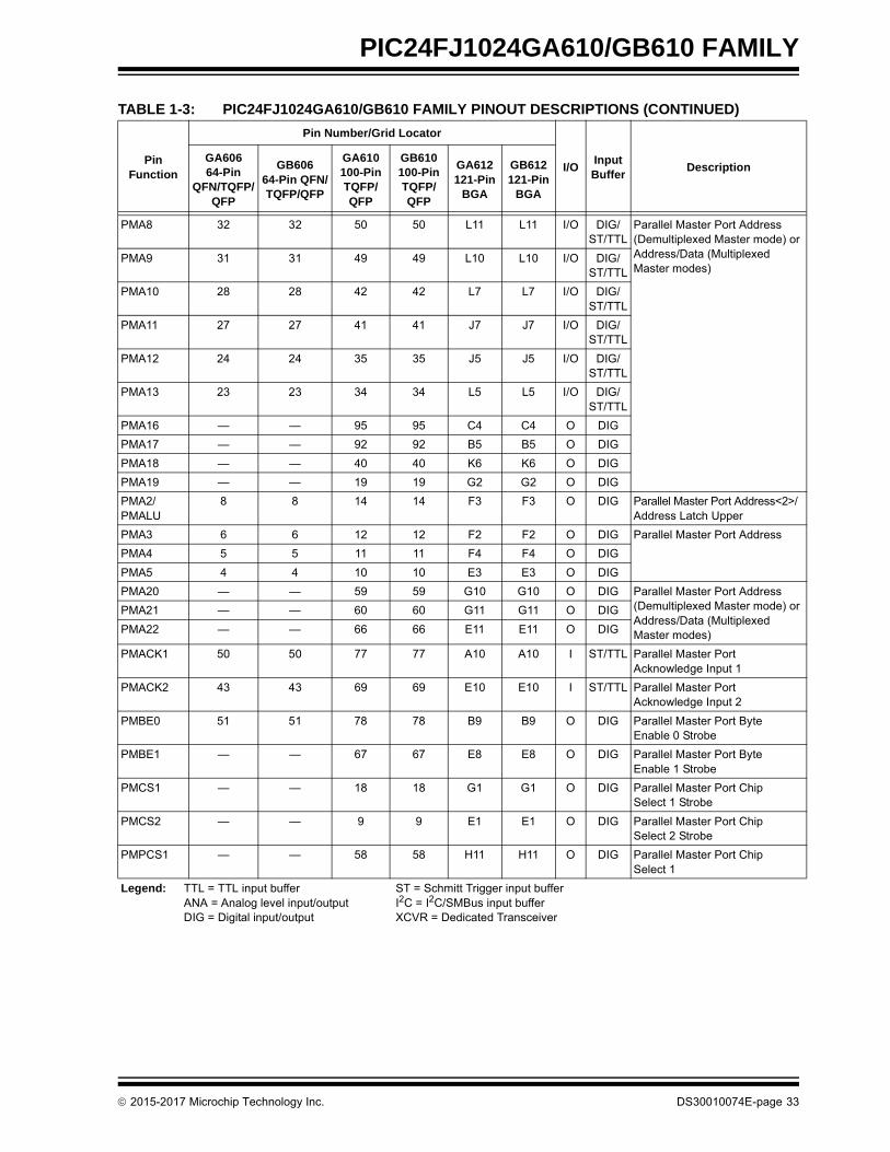
Table 1-3 lists the functions of the various pins shownin the pinout diagrams.
1.1 Core Features
1.1.1 16-BIT ARCHITECTURE
Central to all PIC24F devices is the 16-bit modifiedHarvard architecture, first introduced with Microchip’sdsPIC® Digital Signal Controllers (DSCs). The PIC24FCPU core offers a wide range of enhancements, suchas:
• 16-bit data and 24-bit address paths with the ability to move information between data and memory spaces
• Linear addressing of up to 12 Mbytes (program space) and 32 Kbytes (data)
• A 16-element Working register array with built-in software stack support
• A 17 x 17 hardware multiplier with support for integer math
• Hardware support for 32 by 16-bit division
• An instruction set that supports multiple addressing modes and is optimized for high-level languages, such as ‘C’
• Operational performance up to 16 MIPS
1.1.2 POWER-SAVING TECHNOLOGY
The PIC24FJ1024GA610/GB610 family of devicesincludes Retention Sleep, a low-power mode withessential circuits being powered from a separatelow-voltage regulator.
This new low-power mode also supports the continuousoperation of the low-power, on-chip Real-Time Clock/Calendar (RTCC), making it possible for an applicationto keep time while the device is otherwise asleep.
Aside from this new feature, PIC24FJ1024GA610/GB610family devices also include all of the legacy power-savingfeatures of previous PIC24F microcontrollers, such as:
• On-the-Fly Clock Switching, allowing the selection of a lower power clock during run time
• Doze Mode Operation, for maintaining peripheral clock speed while slowing the CPU clock
• Instruction-Based Power-Saving Modes, for quick invocation of the Idle and the Sleep modes
1.1.3 OSCILLATOR OPTIONS AND FEATURES
All of the devices in the PIC24FJ1024GA610/GB610family offer six different oscillator options, allowingusers a range of choices in developing applicationhardware. These include:
• Two Crystal modes
• Two External Clock (EC) modes
• A Phase-Locked Loop (PLL) frequency multiplier, which allows clock speeds of up to 32 MHz
• A Digitally Controlled Oscillator (DCO) with multiple frequencies and fast wake-up time
• A Fast Internal Oscillator (FRC), a nominal 8 MHz output, with multiple frequency divider options
• A separate Low-Power Internal RC Oscillator (LPRC), 31 kHz nominal, for low-power, timing-insensitive applications.
The internal oscillator block also provides a stablereference source for the Fail-Safe Clock Monitor(FSCM). This option constantly monitors the main clocksource against a reference signal provided by the inter-nal oscillator and enables the controller to switch to theinternal oscillator, allowing for continued low-speedoperation or a safe application shutdown.
1.1.4 EASY MIGRATION
Regardless of the memory size, all devices share thesame rich set of peripherals, allowing for a smoothmigration path as applications grow and evolve. Theconsistent pinout scheme used throughout the entirefamily also aids in migrating from one device to the nextlarger device, or even in jumping from 64-pin to 100-pindevices.
The PIC24F family is pin-compatible with devices in thedsPIC33 family, and shares some compatibility with thepinout schema for PIC18 and dsPIC30. This extendsthe ability of applications to grow from the relativelysimple, to the powerful and complex, yet still selectinga Microchip device.
• PIC24FJ1024GB610 • PIC24FJ1024GA610
• PIC24FJ512GB610 • PIC24FJ512GA610
• PIC24FJ256GB610 • PIC24FJ256GA610
• PIC24FJ128GB610 • PIC24FJ128GA610
• PIC24FJ1024GB606 • PIC24FJ1024GA606
• PIC24FJ512GB606 • PIC24FJ512GA606
• PIC24FJ256GB606 • PIC24FJ256GA606
• PIC24FJ128GB606 • PIC24FJ128GA606
2015-2017 Microchip Technology Inc. DS30010074E-page 21

PIC24FJ1024GA610/GB610 FAMILY
1.2 DMA Controller
PIC24FJ1024GA610/GB610 family devices have a DirectMemory Access (DMA) Controller. This module acts inconcert with the CPU, allowing data to move betweendata memory and peripherals without the intervention ofthe CPU, increasing data throughput and decreasing exe-cution time overhead. Eight independently programmablechannels make it possible to service multiple peripheralsat virtually the same time, with each channel peripheralperforming a different operation. Many types of datatransfer operations are supported.
1.3 Other Special Features
• Peripheral Pin Select: The Peripheral Pin Select (PPS) feature allows most digital peripherals to be mapped over a fixed set of digital I/O pins. Users may independently map the input and/or output of any one of the many digital peripherals to any one of the I/O pins.
• Configurable Logic Cell: The Configurable Logic Cell (CLC) module allows the user to specify combinations of signals as inputs to a logic function and to use the logic output to control other peripherals or I/O pins.
• Timing Modules: The PIC24FJ1024GA610/GB610 family provides five independent, general purpose, 16-bit timers (four of which can be combined into two 32-bit timers). The devices also include 3 multiple output and 4 single output advanced Capture/Compare/PWM/Timer peripherals, and 6 independent legacy Input Capture and 6 independent legacy Output Compare modules.
• Communications: The PIC24FJ1024GA610/GB610 family incorporates a range of serial communication peripherals to handle a range of application requirements. There are 3 independent I2C modules that support both Master and Slave modes of operation. Devices also have, through the PPS feature, 6 independent UARTs with built-in IrDA® encoders/decoders and 3 SPI modules.
• Analog Features: All members of the PIC24FJ1024GA610/GB610 family include the new 12-bit A/D Converter (A/D) module and a triple comparator module. The A/D module incor-porates a range of new features that allow the converter to assess and make decisions on incoming data, reducing CPU overhead for routine A/D conversions. The comparator module includes three analog comparators that are configurable for a wide range of operations.
• CTMU Interface: In addition to their other analog features, members of the PIC24FJ1024GA610/GB610 family include the CTMU interface module. This provides a convenient method for precision time measurement and pulse generation, and can serve as an interface for capacitive sensors.
• Enhanced Parallel Master/Parallel Slave Port: This module allows rapid and transparent access to the microcontroller data bus, and enables the CPU to directly address external data memory. The parallel port can function in Master or Slave mode, accommodating data widths of 4, 8 or 16 bits and address widths of up to 23 bits in Master modes.
• Real-Time Clock and Calendar (RTCC): This module implements a full-featured clock and calendar with alarm functions in hardware, freeing up timer resources and program memory space for use of the core application.
1.4 Details on Individual Family Members
Devices in the PIC24FJ1024GA610/GB610 family areavailable in 64-pin, 100-pin and 121-pin packages. Thegeneral block diagram for all devices is shown inFigure 1-1.
The devices are differentiated from each other insix ways:
1. Flash program memory (128 Kbytes forPIC24FJ128GX6XX devices, 256 Kbytes forPIC24FJ256GX6XX devices, 512 Kbytes forPIC24FJ512GX6XX devices and 1024 Kbytesfor PIC24FJ1024GX6XX devices).
2. Available I/O pins and ports (53 pins on 6 portsfor 64-pin devices and 85 pins on 7 ports for100-pin and 121-pin devices).
3. Available Interrupt-on-Change Notification (IOC)inputs (53 on 64-pin devices and 85 on 100-pinand 121-pin devices).
4. Available remappable pins (29 pins on 64-pindevices, 44 pins on 100-pin and 121-pindevices).
5. Available USB peripheral (available onPIC24FJXXXGB6XX devices; not available onPIC24FJXXXGA6XX devices).
6. Analog input channels (16 channels for 64-pindevices and 24 channels for 100-pin and 121-pindevices).
All other features for devices in this family are identical.These are summarized in Table 1-1, Table 1-2 andTable 1-3.
A list of the pin features available on thePIC24FJ1024GA610/GB610 family devices, sortedby function, is shown in Table 1-3. Note that this tableshows the pin location of individual peripheral featuresand not how they are multiplexed on the same pin. Thisinformation is provided in the pinout diagrams in thebeginning of this data sheet. Multiplexed features aresorted by the priority given to a feature, with the highestpriority peripheral being listed first.
DS30010074E-page 22 2015-2017 Microchip Technology Inc.

PIC24FJ1024GA610/GB610 FAMILY
TABLE 1-1: DEVICE FEATURES FOR THE PIC24FJ1024GA606/GB606: 64-PIN DEVICES
Features PIC24FJ128GX606 PIC24FJ256GX606 PIC24FJ512GX606 PIC24FJ1024GX606
Operating Frequency DC – 32 MHz
Program Memory (bytes) 128K 256K 512K 1024K
Program Memory (instructions) 44,032 88,064 176,128 352,256
Data Memory (bytes) 32K
Interrupt Sources (soft vectors/NMI traps)
103 (97/6)
I/O Ports Ports B, C, D, E, F, G
Total I/O Pins 53
Remappable Pins 29 (28 I/O, 1 input only)
Timers: 5(1)
Total Number (16-bit)
32-Bit (from paired 16-bit timers) 2
Input Capture Channels 6(1)
Output Compare/PWM Channels 6(1)
Input Change Notification Interrupt 53
Serial Communications: 6(1)
UART
SPI (3-wire/4-wire) 3(1)
I2C 3
Configurable Logic Cell (CLC) 4(1)
Parallel Communications (EPMP/PSP)
Yes
Capture/Compare/PWM/Timer Modules
3 Multiple Outputs and 4 Single Outputs
JTAG Boundary Scan Yes
12/10-Bit Analog-to-Digital Converter (A/D) Module (input channels)
16
Analog Comparators 3
CTMU Interface Yes
Universal Serial Bus Controller Yes (PIC24FJ1024GB606 devices only)
Resets (and Delays) Core POR, VDD POR, BOR, RESET Instruction, MCLR, WDT, Illegal Opcode, REPEAT Instruction, Hardware Traps, Configuration Word Mismatch
(OST, PLL Lock)
Instruction Set 76 Base Instructions, Multiple Addressing Mode Variations
Packages 64-Pin TQFP and QFN
Note 1: Some peripherals are accessible through remappable pins.
2015-2017 Microchip Technology Inc. DS30010074E-page 23

PIC24FJ1024GA610/GB610 FAMILY
TABLE 1-2: DEVICE FEATURES FOR THE PIC24FJ1024GX610: 100-PIN AND 121-PIN DEVICES
Features PIC24FJ128GX610 PIC24FJ256GX610 PIC24FJ512GX610 PIC24FJ1024GX610
Operating Frequency DC – 32 MHz
Program Memory (bytes) 128K 256K 512K 1024K
Program Memory (instructions) 44,032 88,064 176,128 352,256
Data Memory (bytes) 32K
Interrupt Sources (soft vectors/NMI traps)
103 (97/6)
I/O Ports Ports A, B, C, D, E, F, G
Total I/O Pins 85
Remappable Pins 44 (32 I/O, 12 input only)
Timers: 5(1)
Total Number (16-bit)
32-Bit (from paired 16-bit timers) 2
Capture/Compare/PWM/Timer Modules
3 Multiple Outputs and 4 Single Outputs
Input Capture Channels 6(1)
Output Compare/PWM Channels 6(1)
Input Change Notification Interrupt 85
Serial Communications: 6(1)
UART
SPI (3-wire/4-wire) 3(1)
I2C 3
Configurable Logic Cell (CLC 4
Parallel Communications (EPMP/PSP)
Yes
JTAG Boundary Scan Yes
12/10-Bit Analog-to-Digital Converter (A/D) Module (input channels)
24
Analog Comparators 3
CTMU Interface Yes
Universal Serial Bus Controller Yes (PIC14FJ1024GB610 devices only)
Resets (and delays) Core POR, VDD POR, BOR, RESET Instruction, MCLR, WDT, Illegal Opcode, REPEAT Instruction, Hardware Traps, Configuration Word Mismatch
(OST, PLL Lock)
Instruction Set 76 Base Instructions, Multiple Addressing Mode Variations
Packages 100-Pin TQFP and 121-Pin BGA
Note 1: Some peripherals are accessible through remappable pins.
DS30010074E-page 24 2015-2017 Microchip Technology Inc.

PIC24FJ1024GA610/GB610 FAMILY
FIGURE 1-1: PIC24FJ1024GA610/GB610 FAMILY GENERAL BLOCK DIAGRAM
InstructionDecode and
Control
16
PCH
16
Program Counter
16-Bit ALU
23
24
Data Bus
Inst Register
16
DivideSupport
Inst Latch
16
EA MUX
Read AGUWrite AGU
16
16
8
Interrupt
Controller
EDS and
StackControlLogic
RepeatControlLogic
Data Latch
Data RAM
AddressLatch
Address Latch
Extended Data
Data Latch
16
Address Bus
Literal
23
Control Signals
16
16
16 x 16W Reg Array
Multiplier17x17OSCI/CLKI
OSCO/CLKO
VDD, VSS
TimingGeneration
MCLR
Power-upTimer
OscillatorStart-up Timer
Power-onReset
WatchdogTimer
HLVD &
Precision
ReferenceBand Gap
FRC/LPRCOscillators
RegulatorsVoltage
VCAP
PORTA(1)
PORTC(1)
(12 I/O)
(8 I/O)
PORTB
(16 I/O)
Note 1: Not all I/O pins or features are implemented on all device pinout configurations. See Table 1-3 for specific implementations by pin count.2: BOR functionality is provided when the on-board voltage regulator is enabled.3: Some peripheral I/Os are only accessible through remappable pins.
PORTD(1)
(16 I/O)
Comparators(3)Timer2/3(3)Timer1 RTCC
IC
A/D12-Bit
OC/PWM SPI I2C
Timer4/5(3)
EPMP/PSP
1-6(3) IOCs(1) UART
REFO
PORTE(1)
PORTG(1)
(10 I/O)
(12 I/O)
PORTF(1)
(11 I/O)
1-3(3) 1-3 1-6(3)1-6(3) CTMUUSB
Driver
Space
Program Memory/
CLC1-4(1)
DMAController
Data
DMAData Bus
16
Table DataAccess Control
MCCP1/2/3
SCCP4/5/6/7
PCL
BOR(2)
2015-2017 Microchip Technology Inc. DS30010074E-page 25

PIC24FJ1024GA610/GB610 FAMILY
TABLE 1-3: PIC24FJ1024GA610/GB610 FAMILY PINOUT DESCRIPTIONS
PinFunction
Pin Number/Grid Locator
I/OInputBuffer
DescriptionGA606 64-Pin
QFN/TQFP/QFP
GB606 64-Pin QFN/TQFP/QFP
GA610 100-Pin TQFP/QFP
GB610 100-Pin TQFP/QFP
GA612 121-Pin
BGA
GB612 121-Pin
BGA
AN0 16 16 25 25 K2 K2 I ANA A/D Analog Inputs
AN1 15 15 24 24 K1 K1 I ANA
AN2 14 14 23 23 J2 J2 I ANA
AN3 13 13 22 22 J1 J1 I ANA
AN4 12 12 21 21 H2 H2 I ANA
AN5 11 11 20 20 H1 H1 I ANA
AN6 17 17 26 26 L1 L1 I ANA
AN7 18 18 27 27 J3 J3 I ANA
AN8 21 21 32 32 K4 K4 I ANA
AN9 22 22 33 33 L4 L4 I ANA
AN10 23 23 34 34 L5 L5 I ANA
AN11 24 24 35 35 J5 J5 I ANA
AN12 27 27 41 41 J7 J7 I ANA
AN13 28 28 42 42 L7 L7 I ANA
AN14 29 29 43 43 K7 K7 I ANA
AN15 30 30 44 44 L8 L8 I ANA
AN16 — — 9 9 E1 E1 I ANA
AN17 — — 10 10 E3 E3 I ANA
AN18 — — 11 11 F4 F4 I ANA
AN19 — — 12 12 F2 F2 I ANA
AN20 — — 14 14 F3 F3 I ANA
AN21 — — 19 19 G2 G2 I ANA
AN22 — — 92 92 B5 B5 I ANA
AN23 — — 91 91 C5 C5 I ANA
AVDD 19 19 30 30 J4 J4 P — Positive Supply for Analog modules
AVSS 20 20 31 31 L3 L3 P — Ground Reference for Analog modules
C1INA 11 11 20 20 H1 H1 I ANA Comparator 1 Input A
C1INB 12 12 21 21 H2 H2 I ANA Comparator 1 Input B
C1INC 5,8 5,8 11,14 11,14 F4,F3 F4,F3 I ANA Comparator 1 Input C
C1IND 4 4 10 10 E3 E3 I ANA Comparator 1 Input D
C2INA 13 13 22 22 J1 J1 I ANA Comparator 2 Input A
C2INB 14 14 23 23 J2 J2 I ANA Comparator 2 Input B
C2INC 8 8 14 14 F3 F3 I ANA Comparator 2 Input C
C2IND 6 6 12 12 F2 F2 I ANA Comparator 2 Input D
C3INA 55 55 84 84 C7 C7 I ANA Comparator 3 Input A
Legend: TTL = TTL input buffer ST = Schmitt Trigger input bufferANA = Analog level input/output I2C = I2C/SMBus input bufferDIG = Digital input/output XCVR = Dedicated Transceiver
DS30010074E-page 26 2015-2017 Microchip Technology Inc.

PIC24FJ1024GA610/GB610 FAMILY
C3INB 54 54 83 83 D7 D7 I ANA Comparator 3 Input B
C3INC 8,48 8,48 14,74 14,74 F3,B11 F3,B11 I ANA Comparator 3 Input C
C3IND 47 47 73 73 C10 C10 I ANA Comparator 3 Input D
CLC3OUT 46 46 72 72 D9 D9 O DIG CLC3 Output
CLC4OUT 42 42 68 68 E9 E9 O DIG CLC4 Output
CLKI 39 39 63 63 F9 F9 — — Main Clock Input Connection
CLKO 40 40 64 64 F11 F11 O DIG System Clock Output
CTCMP 14 14 23 23 J2 J2 O ANA CTMU Comparator 2 Input (Pulse mode)
CTED1 28 28 42 42 L7 L7 I ST CTMU External Edge Inputs
CTED2 27 27 41 41 J7 J7 I ST
CTED3 — — 1 1 B2 B2 I ST
CTED4 1 1 3 3 D3 D3 I ST
CTED5 29 29 43 43 K7 K7 I ST
CTED6 30 30 44 44 L8 L8 I ST
CTED7 — — 40 40 K6 K6 I ST
CTED8 64 64 100 100 A1 A1 I ST
CTED9 63 63 99 99 A2 A2 I ST
CTED10 — — 97 97 A3 A3 I ST
CTED11 — — 95 95 C4 C4 I ST
CTED12 15 15 24 24 K1 K1 I ST
CTED13 14 14 23 23 J2 J2 I ST
CTPLS 29 29 43 43 K7 K7 O DIG CTMU Pulse Output
CVREF 23 23 34 34 L5 L5 O ANA Comparator Voltage Reference Output
CVREF+ 16 16 25,29 25,29 K2,K3 K2,K3 I ANA Comparator Voltage Reference (high) Input
CVREF- 15 15 24,28 24,28 K1,L2 K1,L2 I ANA Comparator Voltage Reference (low) Input
D+ — 37 — 57 — H10 I/O XCVR USB Signaling
D- — 36 — 56 — J11 I/O XCVR
TABLE 1-3: PIC24FJ1024GA610/GB610 FAMILY PINOUT DESCRIPTIONS (CONTINUED)
PinFunction
Pin Number/Grid Locator
I/OInputBuffer
DescriptionGA606 64-Pin
QFN/TQFP/QFP
GB606 64-Pin QFN/TQFP/QFP
GA610 100-Pin TQFP/QFP
GB610 100-Pin TQFP/QFP
GA612 121-Pin
BGA
GB612 121-Pin
BGA
Legend: TTL = TTL input buffer ST = Schmitt Trigger input bufferANA = Analog level input/output I2C = I2C/SMBus input bufferDIG = Digital input/output XCVR = Dedicated Transceiver
2015-2017 Microchip Technology Inc. DS30010074E-page 27

PIC24FJ1024GA610/GB610 FAMILY
IC4 1 1 3 3 D3 D3 I ST Input Capture
IC5 2 2 4 4 C1 C1 I ST
IC6 3 3 5 5 D2 D2 I ST
ICM1 4 4 10 10 12 12 I ST MCCP1 Input Capture
ICM2 6 6 12 12 14 14 I ST MCCP2 Input Capture
ICM3 11 11 20 20 23 23 I ST MCCP3 Input Capture
ICM4 49 49 76 76 91 91 I ST SCCP4 Input Capture
ICM5 42 42 68 68 80 80 I ST SCCP5 Input Capture
ICM6 46 46 72 72 86 86 I ST SCCP6 Input Capture
ICM7 51 51 78 78 93 93 I ST SCCP7 Input Capture
INT0 35 46 55 72 H9 D9 I ST External Interrupt Input 0
IOCA0 — — 17 17 G3 G3 I ST PORTA Interrupt-on-Change
IOCA1 — — 38 38 J6 J6 I ST
IOCA2 — — 58 58 H11 H11 I ST
IOCA3 — — 59 59 G10 G10 I ST
IOCA4 — — 60 60 G11 G11 I ST
IOCA5 — — 61 61 G9 G9 I ST
IOCA6 — — 91 91 C5 C5 I ST
IOCA7 — — 92 92 B5 B5 I ST
IOCA9 — — 28 28 L2 L2 I ST
IOCA10 — — 29 29 K3 K3 I ST
IOCA14 — — 66 66 E11 E11 I ST
IOCA15 — — 67 67 E8 E8 I ST
TABLE 1-3: PIC24FJ1024GA610/GB610 FAMILY PINOUT DESCRIPTIONS (CONTINUED)
PinFunction
Pin Number/Grid Locator
I/OInputBuffer
DescriptionGA606 64-Pin
QFN/TQFP/QFP
GB606 64-Pin QFN/TQFP/QFP
GA610 100-Pin TQFP/QFP
GB610 100-Pin TQFP/QFP
GA612 121-Pin
BGA
GB612 121-Pin
BGA
Legend: TTL = TTL input buffer ST = Schmitt Trigger input bufferANA = Analog level input/output I2C = I2C/SMBus input bufferDIG = Digital input/output XCVR = Dedicated Transceiver
DS30010074E-page 28 2015-2017 Microchip Technology Inc.

PIC24FJ1024GA610/GB610 FAMILY
IOCB0 16 16 25 25 K2 K2 I ST PORTB Interrupt-on-Change
IOCB1 15 15 24 24 K1 K1 I ST
IOCB2 14 14 23 23 J2 J2 I ST
IOCB3 13 13 22 22 J1 J1 I ST
IOCB4 12 12 21 21 H2 H2 I ST
IOCB5 11 11 20 20 H1 H1 I ST
IOCB6 17 17 26 26 L1 L1 I ST
IOCB7 18 18 27 27 J3 J3 I ST
IOCB8 21 21 32 32 K4 K4 I ST
IOCB9 22 22 33 33 L4 L4 I ST
IOCB10 23 23 34 34 L5 L5 I ST
IOCB11 24 24 35 35 J5 J5 I ST
IOCB12 27 27 41 41 J7 J7 I ST
IOCB13 28 28 42 42 L7 L7 I ST
IOCB14 29 29 43 43 K7 K7 I ST
IOCB15 30 30 44 44 L8 L8 I ST
IOCC1 — — 6 6 D1 D1 I ST PORTC Interrupt-on-Change
IOCC2 — — 7 7 E4 E4 I ST
IOCC3 — — 8 8 E2 E2 I ST
IOCC4 — — 9 9 E1 E1 I ST
IOCC12 39 39 63 63 F9 F9 I ST
IOCC13 47 47 73 73 C10 C10 I ST
IOCC14 48 48 74 74 B11 B11 I ST
IOCC15 40 40 64 64 F11 F11 I ST
TABLE 1-3: PIC24FJ1024GA610/GB610 FAMILY PINOUT DESCRIPTIONS (CONTINUED)
PinFunction
Pin Number/Grid Locator
I/OInputBuffer
DescriptionGA606 64-Pin
QFN/TQFP/QFP
GB606 64-Pin QFN/TQFP/QFP
GA610 100-Pin TQFP/QFP
GB610 100-Pin TQFP/QFP
GA612 121-Pin
BGA
GB612 121-Pin
BGA
Legend: TTL = TTL input buffer ST = Schmitt Trigger input bufferANA = Analog level input/output I2C = I2C/SMBus input bufferDIG = Digital input/output XCVR = Dedicated Transceiver
2015-2017 Microchip Technology Inc. DS30010074E-page 29

PIC24FJ1024GA610/GB610 FAMILY
IOCD0 46 46 72 72 D9 D9 I ST PORTD Interrupt-on-Change
IOCD1 49 49 76 76 A11 A11 I ST
IOCD2 50 50 77 77 A10 A10 I ST
IOCD3 51 51 78 78 B9 B9 I ST
IOCD4 52 52 81 81 C8 C8 I ST
IOCD5 53 53 82 82 B8 B8 I ST
IOCD6 54 54 83 83 D7 D7 I ST
IOCD7 55 55 84 84 C7 C7 I ST
IOCD8 42 42 68 68 E9 E9 I ST
IOCD9 43 43 69 69 E10 E10 I ST
IOCD10 44 44 70 70 D11 D11 I ST
IOCD11 45 45 71 71 C11 C11 I ST
IOCD12 — — 79 79 A9 A9 I ST
IOCD13 — — 80 80 D8 D8 I ST
IOCD14 — — 47 47 L9 L9 I ST
IOCD15 — — 48 48 K9 K9 I ST
IOCE0 60 60 93 93 A4 A4 I ST PORTE Interrupt-on-Change
IOCE1 61 61 94 94 B4 B4 I ST
IOCE2 62 62 98 98 B3 B3 I ST
IOCE3 63 63 99 99 A2 A2 I ST
IOCE4 64 64 100 100 A1 A1 I ST
IOCE5 1 1 3 3 D3 D3 I ST
IOCE6 2 2 4 4 C1 C1 I ST
IOCE7 3 3 5 5 D2 D2 I ST
IOCE8 — — 18 18 G1 G1 I ST
IOCE9 — — 19 19 G2 G2 I ST
TABLE 1-3: PIC24FJ1024GA610/GB610 FAMILY PINOUT DESCRIPTIONS (CONTINUED)
PinFunction
Pin Number/Grid Locator
I/OInputBuffer
DescriptionGA606 64-Pin
QFN/TQFP/QFP
GB606 64-Pin QFN/TQFP/QFP
GA610 100-Pin TQFP/QFP
GB610 100-Pin TQFP/QFP
GA612 121-Pin
BGA
GB612 121-Pin
BGA
Legend: TTL = TTL input buffer ST = Schmitt Trigger input bufferANA = Analog level input/output I2C = I2C/SMBus input bufferDIG = Digital input/output XCVR = Dedicated Transceiver
DS30010074E-page 30 2015-2017 Microchip Technology Inc.

PIC24FJ1024GA610/GB610 FAMILY
IOCF0 58 58 87 87 B6 B6 I ST PORTF Interrupt-on-Change
IOCF1 59 59 88 88 A6 A6 I ST
IOCF2 34 — 52 52 K11 K11 I ST
IOCF3 33 33 51 51 K10 K10 I ST
IOCF4 31 31 49 49 L10 L10 I ST
IOCF5 32 32 50 50 L11 L11 I ST
IOCF6 35 — 55 — H9 — I ST
IOCF7 — 34 54 54 H8 H8 I ST
IOCF8 — — 53 53 J10 J10 I ST
IOCF12 — — 40 40 K6 K6 I ST
IOCF13 — — 39 39 L6 L6 I ST
IOCG0 — — 90 90 A5 A5 I ST PORTG Interrupt-on-Change
IOCG1 — — 89 89 E6 E6 I ST
IOCG2 37 37 57 57 H10 H10 I ST
IOCG3 36 36 56 56 J11 J11 I ST
IOCG6 4 4 10 10 E3 E3 I ST
IOCG7 5 5 11 11 F4 F4 I ST
IOCG8 6 6 12 12 F2 F2 I ST
IOCG9 8 8 14 14 F3 F3 I ST
IOCG12 — — 96 96 C3 C3 I ST
IOCG13 — — 97 97 A3 A3 I ST
IOCG14 — — 95 95 C4 C4 I ST
IOCG15 — — 1 1 B2 B2 I ST
HLVDIN 64 64 100 100 A1 A1 I ANA High/Low-Voltage Detect Input
MCLR 7 7 13 13 F1 F1 I ST Master Clear (device Reset) Input. This line is brought low to cause a Reset.
OC4 54 54 83 83 D7 D7 O DIG Output Compare Outputs
OC5 55 55 84 84 C7 C7 O DIG
OC6 58 58 87 87 B6 B6 O DIG
OCM1A 4 4 10 10 E3 E3 O DIG MCCP1 Outputs
OCM1B 5 5 11 11 F4 F4 O DIG
OCM1C — — 1 1 B2 B2 O DIG
OCM1D — — 6 6 D1 D1 O DIG
OCM1E — — 91 91 C5 C5 O DIG
OCM1F — — 92 92 B5 B5 O DIG
TABLE 1-3: PIC24FJ1024GA610/GB610 FAMILY PINOUT DESCRIPTIONS (CONTINUED)
PinFunction
Pin Number/Grid Locator
I/OInputBuffer
DescriptionGA606 64-Pin
QFN/TQFP/QFP
GB606 64-Pin QFN/TQFP/QFP
GA610 100-Pin TQFP/QFP
GB610 100-Pin TQFP/QFP
GA612 121-Pin
BGA
GB612 121-Pin
BGA
Legend: TTL = TTL input buffer ST = Schmitt Trigger input bufferANA = Analog level input/output I2C = I2C/SMBus input bufferDIG = Digital input/output XCVR = Dedicated Transceiver
2015-2017 Microchip Technology Inc. DS30010074E-page 31

PIC24FJ1024GA610/GB610 FAMILY
OCM2A 6 6 12 12 F2 F2 O DIG MCCP2 Outputs
OCM2B 8 8 14 14 F3 F3 O DIG
OCM2C — — 7 7 E4 E4 O DIG
OCM2D — — 8 8 E2 E2 O DIG
OCM2E — — 96 96 C3 C3 O DIG
OCM2F — — 97 97 A3 A3 O DIG
OCM3A 11 11 20 20 H1 H1 O DIG MCCP3 Outputs
OCM3B 12 12 21 21 H2 H2 O DIG
OCM3C — — 9 9 E1 E1 O DIG
OCM3D — — 17 17 G3 G3 O DIG
OCM3E — — 79 79 A9 A9 O DIG
OCM3F — — 80 80 D8 D8 O DIG
OSCI 39 39 63 63 F9 F9 I ANA/ST
Main Oscillator Input Connection
OSCO 40 40 64 64 F11 F11 O ANA Main Oscillator Output Connection
PGEC1 15 15 24 24 K1 K1 I ST ICSP™ Programming Clock
PGEC2 17 17 26 26 L1 L1 I ST
PGEC3 11 11 20 20 H1 H1 I ST
PGED1 16 16 25 25 K2 K2 I/O DIG/ST ICSP Programming Data
PGED2 18 18 27 27 J3 J3 I/O DIG/ST
PGED3 12 12 21 21 H2 H2 I/O DIG/ST
PMA0/PMALL
30 30 44 44 L8 L8 I/O DIG/ST/TTL
Parallel Master Port Address<0>/Address Latch Low
PMA1/PMALH
29 29 43 43 K7 K7 I/O DIG/ST/TTL
Parallel Master Port Address<1>/Address Latch High
PMA14/PMCS1
45 45 71 71 C11 C11 I/O DIG/ST/TTL
Parallel Master Port Address<14>/Slave Chip Select/Chip Select 1 Strobe
PMA15/PMCS2
44 44 70 70 D11 D11 I/O DIG/ST/TTL
Parallel Master Port Address<15>/Chip Select 2 Strobe
PMA6 16 16 29 29 K3 K3 O DIG Parallel Master Port Address
PMA7 22 22 28 28 L2 L2 O DIG
TABLE 1-3: PIC24FJ1024GA610/GB610 FAMILY PINOUT DESCRIPTIONS (CONTINUED)
PinFunction
Pin Number/Grid Locator
I/OInputBuffer
DescriptionGA606 64-Pin
QFN/TQFP/QFP
GB606 64-Pin QFN/TQFP/QFP
GA610 100-Pin TQFP/QFP
GB610 100-Pin TQFP/QFP
GA612 121-Pin
BGA
GB612 121-Pin
BGA
Legend: TTL = TTL input buffer ST = Schmitt Trigger input bufferANA = Analog level input/output I2C = I2C/SMBus input bufferDIG = Digital input/output XCVR = Dedicated Transceiver
DS30010074E-page 32 2015-2017 Microchip Technology Inc.
PIC24FJ1024GA610/GB610 FAMILY
PMA8 32 32 50 50 L11 L11 I/O DIG/ST/TTL
Parallel Master Port Address (Demultiplexed Master mode) or Address/Data (Multiplexed Master modes)
PMA9 31 31 49 49 L10 L10 I/O DIG/ST/TTL
PMA10 28 28 42 42 L7 L7 I/O DIG/ST/TTL
PMA11 27 27 41 41 J7 J7 I/O DIG/ST/TTL
PMA12 24 24 35 35 J5 J5 I/O DIG/ST/TTL
PMA13 23 23 34 34 L5 L5 I/O DIG/ST/TTL
PMA16 — — 95 95 C4 C4 O DIG
PMA17 — — 92 92 B5 B5 O DIG
PMA18 — — 40 40 K6 K6 O DIG
PMA19 — — 19 19 G2 G2 O DIG
PMA2/PMALU
8 8 14 14 F3 F3 O DIG Parallel Master Port Address<2>/Address Latch Upper
PMA3 6 6 12 12 F2 F2 O DIG Parallel Master Port Address
PMA4 5 5 11 11 F4 F4 O DIG
PMA5 4 4 10 10 E3 E3 O DIG
PMA20 — — 59 59 G10 G10 O DIG Parallel Master Port Address (Demultiplexed Master mode) or Address/Data (Multiplexed Master modes)
PMA21 — — 60 60 G11 G11 O DIG
PMA22 — — 66 66 E11 E11 O DIG
PMACK1 50 50 77 77 A10 A10 I ST/TTL Parallel Master Port Acknowledge Input 1
PMACK2 43 43 69 69 E10 E10 I ST/TTL Parallel Master Port Acknowledge Input 2
PMBE0 51 51 78 78 B9 B9 O DIG Parallel Master Port Byte Enable 0 Strobe
PMBE1 — — 67 67 E8 E8 O DIG Parallel Master Port Byte Enable 1 Strobe
PMCS1 — — 18 18 G1 G1 O DIG Parallel Master Port Chip Select 1 Strobe
PMCS2 — — 9 9 E1 E1 O DIG Parallel Master Port Chip Select 2 Strobe
PMPCS1 — — 58 58 H11 H11 O DIG Parallel Master Port Chip Select 1
TABLE 1-3: PIC24FJ1024GA610/GB610 FAMILY PINOUT DESCRIPTIONS (CONTINUED)
PinFunction
Pin Number/Grid Locator
I/OInputBuffer
DescriptionGA606 64-Pin
QFN/TQFP/QFP
GB606 64-Pin QFN/TQFP/QFP
GA610 100-Pin TQFP/QFP
GB610 100-Pin TQFP/QFP
GA612 121-Pin
BGA
GB612 121-Pin
BGA
Legend: TTL = TTL input buffer ST = Schmitt Trigger input bufferANA = Analog level input/output I2C = I2C/SMBus input bufferDIG = Digital input/output XCVR = Dedicated Transceiver
2015-2017 Microchip Technology Inc. DS30010074E-page 33

PIC24FJ1024GA610/GB610 FAMILY
PMD0 60 60 93 93 A4 A4 I/O DIG/ST/TTL
Parallel Master Port Data (Demultiplexed Master mode) or Address/Data (Multiplexed Master modes)
PMD1 61 61 94 94 B4 B4 I/O DIG/ST/TTL
PMD2 62 62 98 98 B3 B3 I/O DIG/ST/TTL
PMD3 63 63 99 99 A2 A2 I/O DIG/ST/TTL
PMD4 64 64 100 100 A1 A1 I/O DIG/ST/TTL
PMD5 1 1 3 3 D3 D3 I/O DIG/ST/TTL
PMD6 2 2 4 4 C1 C1 I/O DIG/ST/TTL
PMD7 3 3 5 5 D2 D2 I/O DIG/ST/TTL
PMD8 — — 90 90 A5 A5 I/O DIG/ST/TTL
PMD9 — — 89 89 E6 E6 I/O DIG/ST/TTL
PMD10 — — 88 88 A6 A6 I/O DIG/ST/TTL
PMD11 — — 87 87 B6 B6 I/O DIG/ST/TTL
PMD12 — — 79 79 A9 A9 I/O DIG/ST/TTL
PMD13 — — 80 80 D8 D8 I/O DIG/ST/TTL
PMD14 — — 83 83 D7 D7 I/O DIG/ST/TTL
PMD15 — — 84 84 C7 C7 I/O DIG/ST/TTL
PMRD/PMWR
53 53 82 82 B8 B8 I/O DIG/ST/TTL
Parallel Master Port Read Strobe/Write Strobe
PMWR/PMENB
52 52 81 81 C8 C8 I/O DIG/ST/TTL
Parallel Master Port Write Strobe/Enable Strobe
PWRGT 21 21 32 32 K4 K4 O DIG Real-Time Clock Power Control Output
PWRLCLK 48 48 74 74 B11 B11 I ST Real-Time Clock 50/60 Hz Clock Input
TABLE 1-3: PIC24FJ1024GA610/GB610 FAMILY PINOUT DESCRIPTIONS (CONTINUED)
PinFunction
Pin Number/Grid Locator
I/OInputBuffer
DescriptionGA606 64-Pin
QFN/TQFP/QFP
GB606 64-Pin QFN/TQFP/QFP
GA610 100-Pin TQFP/QFP
GB610 100-Pin TQFP/QFP
GA612 121-Pin
BGA
GB612 121-Pin
BGA
Legend: TTL = TTL input buffer ST = Schmitt Trigger input bufferANA = Analog level input/output I2C = I2C/SMBus input bufferDIG = Digital input/output XCVR = Dedicated Transceiver
DS30010074E-page 34 2015-2017 Microchip Technology Inc.

PIC24FJ1024GA610/GB610 FAMILY
RA0 — — 17 17 G3 G3 I/O DIG/ST PORTA Digital I/Os
RA1 — — 38 38 J6 J6 I/O DIG/ST
RA2 — — 58 58 H11 H11 I/O DIG/ST
RA3 — — 59 59 G10 G10 I/O DIG/ST
RA4 — — 60 60 G11 G11 I/O DIG/ST
RA5 — — 61 61 G9 G9 I/O DIG/ST
RA6 — — 91 91 C5 C5 I/O DIG/ST
RA7 — — 92 92 B5 B5 I/O DIG/ST
RA9 — — 28 28 L2 L2 I/O DIG/ST
RA10 — — 29 29 K3 K3 I/O DIG/ST
RA14 — — 66 66 E11 E11 I/O DIG/ST
RA15 — — 67 67 E8 E8 I/O DIG/ST
RB0 16 16 25 25 K2 K2 I/O DIG/ST PORTB Digital I/Os
RB1 15 15 24 24 K1 K1 I/O DIG/ST
RB2 14 14 23 23 J2 J2 I/O DIG/ST
RB3 13 13 22 22 J1 J1 I/O DIG/ST
RB4 12 12 21 21 H2 H2 I/O DIG/ST
RB5 11 11 20 20 H1 H1 I/O DIG/ST
RB6 17 17 26 26 L1 L1 I/O DIG/ST
RB7 18 18 27 27 J3 J3 I/O DIG/ST
RB8 21 21 32 32 K4 K4 I/O DIG/ST
RB9 22 22 33 33 L4 L4 I/O DIG/ST
RB10 23 23 34 34 L5 L5 I/O DIG/ST
RB11 24 24 35 35 J5 J5 I/O DIG/ST
RB12 27 27 41 41 J7 J7 I/O DIG/ST
RB13 28 28 42 42 L7 L7 I/O DIG/ST
RB14 29 29 43 43 K7 K7 I/O DIG/ST
RB15 30 30 44 44 L8 L8 I/O DIG/ST
RC1 — — 6 6 D1 D1 I/O DIG/ST PORTC Digital I/Os
RC2 — — 7 7 E4 E4 I/O DIG/ST
RC3 — — 8 8 E2 E2 I/O DIG/ST
RC4 — — 9 9 E1 E1 I/O DIG/ST
RC12 39 39 63 63 F9 F9 I/O DIG/ST
RC13 47 47 73 73 C10 C10 I/O DIG/ST
RC14 48 48 74 74 B11 B11 I/O DIG/ST
RC15 40 40 64 64 F11 F11 I/O DIG/ST
TABLE 1-3: PIC24FJ1024GA610/GB610 FAMILY PINOUT DESCRIPTIONS (CONTINUED)
PinFunction
Pin Number/Grid Locator
I/OInputBuffer
DescriptionGA606 64-Pin
QFN/TQFP/QFP
GB606 64-Pin QFN/TQFP/QFP
GA610 100-Pin TQFP/QFP
GB610 100-Pin TQFP/QFP
GA612 121-Pin
BGA
GB612 121-Pin
BGA
Legend: TTL = TTL input buffer ST = Schmitt Trigger input bufferANA = Analog level input/output I2C = I2C/SMBus input bufferDIG = Digital input/output XCVR = Dedicated Transceiver
2015-2017 Microchip Technology Inc. DS30010074E-page 35

PIC24FJ1024GA610/GB610 FAMILY
RD0 46 46 72 72 D9 D9 I/O DIG/ST PORTD Digital I/Os
RD1 49 49 76 76 A11 A11 I/O DIG/ST
RD2 50 50 77 77 A10 A10 I/O DIG/ST
RD3 51 51 78 78 B9 B9 I/O DIG/ST
RD4 52 52 81 81 C8 C8 I/O DIG/ST
RD5 53 53 82 82 B8 B8 I/O DIG/ST
RD6 54 54 83 83 D7 D7 I/O DIG/ST
RD7 55 55 84 84 C7 C7 I/O DIG/ST
RD8 42 42 68 68 E9 E9 I/O DIG/ST
RD9 43 43 69 69 E10 E10 I/O DIG/ST
RD10 44 44 70 70 D11 D11 I/O DIG/ST
RD11 45 45 71 71 C11 C11 I/O DIG/ST
RD12 — — 79 79 A9 A9 I/O DIG/ST
RD13 — — 80 80 D8 D8 I/O DIG/ST
RD14 — — 47 47 L9 L9 I/O DIG/ST
RD15 — — 48 48 K9 K9 I/O DIG/ST
RE0 60 60 93 93 A4 A4 I/O DIG/ST PORTE Digital I/Os
RE1 61 61 94 94 B4 B4 I/O DIG/ST
RE2 62 62 98 98 B3 B3 I/O DIG/ST
RE3 63 63 99 99 A2 A2 I/O DIG/ST
RE4 64 64 100 100 A1 A1 I/O DIG/ST
RE5 1 1 3 3 D3 D3 I/O DIG/ST
RE6 2 2 4 4 C1 C1 I/O DIG/ST
RE7 3 3 5 5 D2 D2 I/O DIG/ST
RE8 — — 18 18 G1 G1 I/O DIG/ST
RE9 — — 19 19 G2 G2 I/O DIG/ST
REFI 24 24 35 35 J5 J5 I ST Reference Clock Input
TABLE 1-3: PIC24FJ1024GA610/GB610 FAMILY PINOUT DESCRIPTIONS (CONTINUED)
PinFunction
Pin Number/Grid Locator
I/OInputBuffer
DescriptionGA606 64-Pin
QFN/TQFP/QFP
GB606 64-Pin QFN/TQFP/QFP
GA610 100-Pin TQFP/QFP
GB610 100-Pin TQFP/QFP
GA612 121-Pin
BGA
GB612 121-Pin
BGA
Legend: TTL = TTL input buffer ST = Schmitt Trigger input bufferANA = Analog level input/output I2C = I2C/SMBus input bufferDIG = Digital input/output XCVR = Dedicated Transceiver
DS30010074E-page 36 2015-2017 Microchip Technology Inc.

PIC24FJ1024GA610/GB610 FAMILY
RF0 58 58 87 87 B6 B6 I/O DIG/ST PORTF Digital I/Os
RF1 59 59 88 88 A6 A6 I/O DIG/ST
RF2 34 — 52 52 K11 K11 I/O DIG/ST
RF3 33 33 51 51 K10 K10 I/O DIG/ST
RF4 31 31 49 49 L10 L10 I/O DIG/ST
RF5 32 32 50 50 L11 L11 I/O DIG/ST
RF6 35 — 55 — H9 — I/O DIG/ST
RF7 — 34 54 54 H8 H8 I/O DIG/ST
RF8 — — 53 53 J10 J10 I/O DIG/ST
RF12 — — 40 40 K6 K6 I/O DIG/ST
RF13 — — 39 39 L6 L6 I/O DIG/ST
RG0 — — 90 90 A5 A5 I/O DIG/ST PORTG Digital I/Os
RG1 — — 89 89 E6 E6 I/O DIG/ST
RG2 37 37 57 57 H10 H10 I/O DIG/ST
RG3 36 36 56 56 J11 J11 I/O DIG/ST
RG6 4 4 10 10 E3 E3 I/O DIG/ST
RG7 5 5 11 11 F4 F4 I/O DIG/ST
RG8 6 6 12 12 F2 F2 I/O DIG/ST
RG9 8 8 14 14 F3 F3 I/O DIG/ST
RG12 — — 96 96 C3 C3 I/O DIG/ST
RG13 — — 97 97 A3 A3 I/O DIG/ST
RG14 — — 95 95 C4 C4 I/O DIG/ST
RG15 — — 1 1 B2 B2 I/O DIG/ST
TABLE 1-3: PIC24FJ1024GA610/GB610 FAMILY PINOUT DESCRIPTIONS (CONTINUED)
PinFunction
Pin Number/Grid Locator
I/OInputBuffer
DescriptionGA606 64-Pin
QFN/TQFP/QFP
GB606 64-Pin QFN/TQFP/QFP
GA610 100-Pin TQFP/QFP
GB610 100-Pin TQFP/QFP
GA612 121-Pin
BGA
GB612 121-Pin
BGA
Legend: TTL = TTL input buffer ST = Schmitt Trigger input bufferANA = Analog level input/output I2C = I2C/SMBus input bufferDIG = Digital input/output XCVR = Dedicated Transceiver
2015-2017 Microchip Technology Inc. DS30010074E-page 37

PIC24FJ1024GA610/GB610 FAMILY
RP0 16 16 25 25 K2 K2 I/O DIG/ST Remappable Peripherals (input or output)RP1 15 15 24 24 K1 K1 I/O DIG/ST
RP2 42 42 68 68 E9 E9 I/O DIG/ST
RP3 44 44 70 70 D11 D11 I/O DIG/ST
RP4 43 43 69 69 E10 E10 I/O DIG/ST
RP5 — — 48 48 K9 K9 I/O DIG/ST
RP6 17 17 26 26 L1 L1 I/O DIG/ST
RP7 18 18 27 27 J3 J3 I/O DIG/ST
RP8 21 21 32 32 K4 K4 I/O DIG/ST
RP9 22 22 33 33 L4 L4 I/O DIG/ST
RP10 31 31 49 49 L10 L10 I/O DIG/ST
RP11 46 46 72 72 D9 D9 I/O DIG/ST
RP12 45 45 71 71 C11 C11 I/O DIG/ST
RP13 14 14 23 23 J2 J2 I/O DIG/ST
RP14 29 29 43 43 K7 K7 I/O DIG/ST
RP15 — — 53 53 J10 J10 I/O DIG/ST
RP16 33 33 51 51 K10 K10 I/O DIG/ST
RP17 32 32 50 50 L11 L11 I/O DIG/ST
RP18 11 11 20 20 H1 H1 I/O DIG/ST
RP19 6 6 12 12 F2 F2 I/O DIG/ST
RP20 53 53 82 82 B8 B8 I/O DIG/ST
RP21 4 4 10 10 E3 E3 I/O DIG/ST
RP22 51 51 78 78 B9 B9 I/O DIG/ST
RP23 50 50 77 77 A10 A10 I/O DIG/ST
RP24 49 49 76 76 A11 A11 I/O DIG/ST
RP25 52 52 81 81 C8 C8 I/O DIG/ST
RP26 5 5 11 11 F4 F4 I/O DIG/ST
RP27 8 8 14 14 F3 F3 I/O DIG/ST
RP28 12 12 21 21 H2 H2 I/O DIG/ST
RP29 30 30 44 44 L8 L8 I/O DIG/ST
RP30 34 — 52 52 K11 K11 I/O DIG/ST
RP31 — — 39 39 L6 L6 I/O DIG/ST
TABLE 1-3: PIC24FJ1024GA610/GB610 FAMILY PINOUT DESCRIPTIONS (CONTINUED)
PinFunction
Pin Number/Grid Locator
I/OInputBuffer
DescriptionGA606 64-Pin
QFN/TQFP/QFP
GB606 64-Pin QFN/TQFP/QFP
GA610 100-Pin TQFP/QFP
GB610 100-Pin TQFP/QFP
GA612 121-Pin
BGA
GB612 121-Pin
BGA
Legend: TTL = TTL input buffer ST = Schmitt Trigger input bufferANA = Analog level input/output I2C = I2C/SMBus input bufferDIG = Digital input/output XCVR = Dedicated Transceiver
DS30010074E-page 38 2015-2017 Microchip Technology Inc.
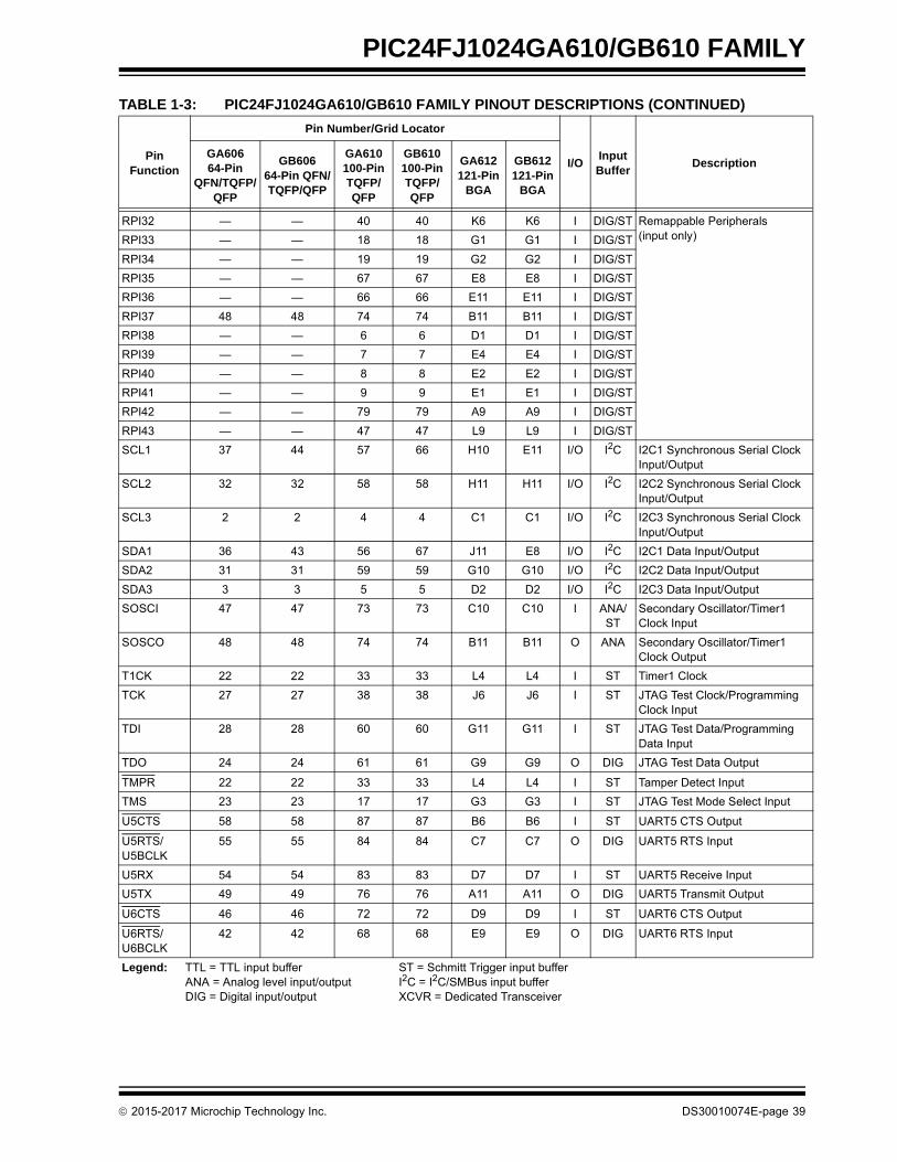
PIC24FJ1024GA610/GB610 FAMILY
RPI32 — — 40 40 K6 K6 I DIG/ST Remappable Peripherals (input only)RPI33 — — 18 18 G1 G1 I DIG/ST
RPI34 — — 19 19 G2 G2 I DIG/ST
RPI35 — — 67 67 E8 E8 I DIG/ST
RPI36 — — 66 66 E11 E11 I DIG/ST
RPI37 48 48 74 74 B11 B11 I DIG/ST
RPI38 — — 6 6 D1 D1 I DIG/ST
RPI39 — — 7 7 E4 E4 I DIG/ST
RPI40 — — 8 8 E2 E2 I DIG/ST
RPI41 — — 9 9 E1 E1 I DIG/ST
RPI42 — — 79 79 A9 A9 I DIG/ST
RPI43 — — 47 47 L9 L9 I DIG/ST
SCL1 37 44 57 66 H10 E11 I/O I2C I2C1 Synchronous Serial Clock Input/Output
SCL2 32 32 58 58 H11 H11 I/O I2C I2C2 Synchronous Serial Clock Input/Output
SCL3 2 2 4 4 C1 C1 I/O I2C I2C3 Synchronous Serial Clock Input/Output
SDA1 36 43 56 67 J11 E8 I/O I2C I2C1 Data Input/Output
SDA2 31 31 59 59 G10 G10 I/O I2C I2C2 Data Input/Output
SDA3 3 3 5 5 D2 D2 I/O I2C I2C3 Data Input/Output
SOSCI 47 47 73 73 C10 C10 I ANA/ST
Secondary Oscillator/Timer1 Clock Input
SOSCO 48 48 74 74 B11 B11 O ANA Secondary Oscillator/Timer1 Clock Output
T1CK 22 22 33 33 L4 L4 I ST Timer1 Clock
TCK 27 27 38 38 J6 J6 I ST JTAG Test Clock/Programming Clock Input
TDI 28 28 60 60 G11 G11 I ST JTAG Test Data/Programming Data Input
TDO 24 24 61 61 G9 G9 O DIG JTAG Test Data Output
TMPR 22 22 33 33 L4 L4 I ST Tamper Detect Input
TMS 23 23 17 17 G3 G3 I ST JTAG Test Mode Select Input
U5CTS 58 58 87 87 B6 B6 I ST UART5 CTS Output
U5RTS/U5BCLK
55 55 84 84 C7 C7 O DIG UART5 RTS Input
U5RX 54 54 83 83 D7 D7 I ST UART5 Receive Input
U5TX 49 49 76 76 A11 A11 O DIG UART5 Transmit Output
U6CTS 46 46 72 72 D9 D9 I ST UART6 CTS Output
U6RTS/U6BCLK
42 42 68 68 E9 E9 O DIG UART6 RTS Input
TABLE 1-3: PIC24FJ1024GA610/GB610 FAMILY PINOUT DESCRIPTIONS (CONTINUED)
PinFunction
Pin Number/Grid Locator
I/OInputBuffer
DescriptionGA606 64-Pin
QFN/TQFP/QFP
GB606 64-Pin QFN/TQFP/QFP
GA610 100-Pin TQFP/QFP
GB610 100-Pin TQFP/QFP
GA612 121-Pin
BGA
GB612 121-Pin
BGA
Legend: TTL = TTL input buffer ST = Schmitt Trigger input bufferANA = Analog level input/output I2C = I2C/SMBus input bufferDIG = Digital input/output XCVR = Dedicated Transceiver
2015-2017 Microchip Technology Inc. DS30010074E-page 39
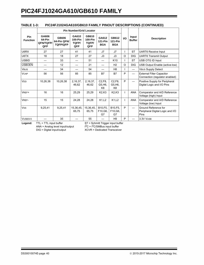
PIC24FJ1024GA610/GB610 FAMILY
U6RX 27 27 41 41 J7 J7 I ST UART6 Receive Input
U6TX 18 18 27 27 J3 J3 O DIG UART6 Transmit Output
USBID — 33 — 51 — K10 I ST USB OTG ID Input
USBOEN — 12 — 21 — H2 O DIG USB Output Enable (active-low)
VBUS — 34 — 54 — H8 I — VBUS Supply Detect
VCAP 56 56 85 85 B7 B7 P — External Filter Capacitor Connection (regulator enabled)
VDD 10,26,38 10,26,38 2,16,37,46,62
2,16,37,46,62
C2,F8,G5,H6,
K8
C2,F8,G5,H6,
K8
P — Positive Supply for Peripheral Digital Logic and I/O Pins
VREF+ 16 16 25,29 25,29 K2,K3 K2,K3 I ANA Comparator and A/D Reference Voltage (high) Input
VREF- 15 15 24,28 24,28 K1,L2 K1,L2 I ANA Comparator and A/D Reference Voltage (low) Input
VSS 9,25,41 9,25,41 15,36,45,65,75
15,36,45,65,75
B10,F5,F10,G6,
G7
B10,F5,F10,G6,
G7
P — Ground Reference for Peripheral Digital Logic and I/O Pins
VUSB3V3 — 35 — 55 — H9 P — 3.3V VUSB
TABLE 1-3: PIC24FJ1024GA610/GB610 FAMILY PINOUT DESCRIPTIONS (CONTINUED)
PinFunction
Pin Number/Grid Locator
I/OInputBuffer
DescriptionGA606 64-Pin
QFN/TQFP/QFP
GB606 64-Pin QFN/TQFP/QFP
GA610 100-Pin TQFP/QFP
GB610 100-Pin TQFP/QFP
GA612 121-Pin
BGA
GB612 121-Pin
BGA
Legend: TTL = TTL input buffer ST = Schmitt Trigger input bufferANA = Analog level input/output I2C = I2C/SMBus input bufferDIG = Digital input/output XCVR = Dedicated Transceiver
DS30010074E-page 40 2015-2017 Microchip Technology Inc.

PIC24FJ1024GA610/GB610 FAMILY
2.0 GUIDELINES FOR GETTING STARTED WITH 16-BIT MICROCONTROLLERS
2.1 Basic Connection Requirements
Getting started with the PIC24FJ1024GA610/GB610family of 16-bit microcontrollers requires attention to aminimal set of device pin connections beforeproceeding with development.
The following pins must always be connected:
• All VDD and VSS pins (see Section 2.2 “Power Supply Pins”)
• The USB transceiver supply, VUSB3V3, regardless of whether or not the USB module is used (see Section 2.2 “Power Supply Pins”)
• All AVDD and AVSS pins, regardless of whether or not the analog device features are used (see Section 2.2 “Power Supply Pins”)
• MCLR pin (see Section 2.3 “Master Clear (MCLR) Pin”)
• VCAP pin (PIC24F J devices only)(see Section 2.4 “Voltage Regulator Pin (VCAP)”)
These pins must also be connected if they are beingused in the end application:
• PGECx/PGEDx pins used for In-Circuit Serial Programming™ (ICSP™) and debugging purposes (see Section 2.5 “ICSP Pins”)
• OSCI and OSCO pins when an external oscillator source is used (see Section 2.6 “External Oscillator Pins”)
Additionally, the following pins may be required:
• VREF+/VREF- pins used when external voltage reference for analog modules is implemented
The minimum mandatory connections are shown inFigure 2-1.
FIGURE 2-1: RECOMMENDED MINIMUM CONNECTIONS
Note: The AVDD and AVSS pins must always beconnected, regardless of whether any ofthe analog modules are being used.
PIC24FJXXXX
VD
D
VS
S
VDD
VSS
VSS
VDD
AV
DD
AV
SS
VD
D
VS
S
C1
R1
VDD
MCLR VCAPR2
C7
C2(2)
C3(2)
C4(2)C5(2)
C6(2)
Key (all values are recommendations):
C1 through C6: 0.1 F, 50V ceramic
C7: 10 F, 16V or greater, ceramic
R1: 10 kΩ
R2: 100Ω to 470Ω
Note 1: See Section 2.4 “Voltage Regulator Pin (VCAP)” for an explanation of voltage regulator pin connections.
2: The example shown is for a PIC24F device with five VDD/VSS and AVDD/AVSS pairs. Other devices may have more or less pairs; adjust the number of decoupling capacitors appropriately.
(1)
2015-2017 Microchip Technology Inc. DS30010074E-page 41

PIC24FJ1024GA610/GB610 FAMILY
2.2 Power Supply Pins
2.2.1 DECOUPLING CAPACITORS
The use of decoupling capacitors on every pair ofpower supply pins, such as VDD, VSS, AVDD andAVSS, is required.
Consider the following criteria when using decouplingcapacitors:
• Value and type of capacitor: A 0.1 F (100 nF), 16V-50V capacitor is recommended. The capacitor should be a low-ESR device with a self-resonance frequency in the range of 200 MHz and higher. Ceramic capacitors are recommended.
• Placement on the printed circuit board: The decoupling capacitors should be placed as close to the pins as possible. It is recommended to place the capacitors on the same side of the board as the device. If space is constricted, the capacitor can be placed on another layer on the PCB using a via; however, ensure that the trace length from the pin to the capacitor is no greater than 0.25 inch (6 mm).
• Handling high-frequency noise: If the board is experiencing high-frequency noise (upward of tens of MHz), add a second ceramic type capaci-tor in parallel to the above described decoupling capacitor. The value of the second capacitor can be in the range of 0.01 F to 0.001 F. Place this second capacitor next to each primary decoupling capacitor. In high-speed circuit designs, consider implementing a decade pair of capacitances as close to the power and ground pins as possible (e.g., 0.1 F in parallel with 0.001 F).
• Maximizing performance: On the board layout from the power supply circuit, run the power and return traces to the decoupling capacitors first, and then to the device pins. This ensures that the decoupling capacitors are first in the power chain. Equally important is to keep the trace length between the capacitor and the power pins to a minimum, thereby reducing PCB trace inductance.
2.2.2 TANK CAPACITORS
On boards with power traces running longer than sixinches in length, it is suggested to use a tank capacitorfor integrated circuits including microcontrollers tosupply a local power source. The value of the tankcapacitor should be determined based on the traceresistance that connects the power supply source tothe device, and the maximum current drawn by thedevice in the application. In other words, select the tankcapacitor so that it meets the acceptable voltage sag atthe device. Typical values range from 4.7 F to 47 F.
2.3 Master Clear (MCLR) Pin
The MCLR pin provides two specific device functions:device Reset, and device programming and debug-ging. If programming and debugging are not requiredin the end application, a direct connection to VDD
may be all that is required. The addition of othercomponents, to help increase the application’sresistance to spurious Resets from voltage sags, maybe beneficial. A typical configuration is shown inFigure 2-1. Other circuit designs may be implementeddepending on the application’s requirements.
During programming and debugging, the resistanceand capacitance that can be added to the pin mustbe considered. Device programmers and debuggersdrive the MCLR pin. Consequently, specific voltagelevels (VIH and VIL) and fast signal transitions mustnot be adversely affected. Therefore, specific valuesof R1 and C1 will need to be adjusted based on theapplication and PCB requirements. For example, it isrecommended that the capacitor, C1, be isolatedfrom the MCLR pin during programming and debug-ging operations by using a jumper (Figure 2-2). Thejumper is replaced for normal run-time operations.
Any components associated with the MCLR pinshould be placed within 0.25 inch (6 mm) of the pin.
FIGURE 2-2: EXAMPLE OF MCLR PIN CONNECTIONS
Note 1: R1 10 k is recommended. A suggestedstarting value is 10 k. Ensure that the MCLRpin VIH and VIL specifications are met.
2: R2 470 will limit any current flowing intoMCLR from the external capacitor, C, in theevent of a MCLR pin breakdown, due toElectrostatic Discharge (ESD) or ElectricalOverstress (EOS). Ensure that the MCLR pinVIH and VIL specifications are met.
C1
R2
R1
VDD
MCLR
PIC24FJXXXXJP
DS30010074E-page 42 2015-2017 Microchip Technology Inc.

PIC24FJ1024GA610/GB610 FAMILY
2.4 Voltage Regulator Pin (VCAP)
Refer to Section 30.3 “On-Chip Voltage Regulator”for details on connecting and using the on-chipregulator.
A low-ESR (< 5Ω) capacitor is required on the VCAP pinto stabilize the voltage regulator output voltage. TheVCAP pin must not be connected to VDD and must use acapacitor of 10 µF connected to ground. The type can beceramic or tantalum. Suitable examples of capacitorsare shown in Table 2-1. Capacitors with equivalentspecifications can be used.
Designers may use Figure 2-3 to evaluate the ESRequivalence of candidate devices.
The placement of this capacitor should be close to VCAP.It is recommended that the trace length not exceed0.25 inch (6 mm). Refer to Section 33.0 “ElectricalCharacteristics” for additional information.
FIGURE 2-3: FREQUENCY vs. ESR PERFORMANCE FOR SUGGESTED VCAP
.
Note: This section applies only to PIC24FJdevices with an on-chip voltage regulator.
10
1
0.1
0.01
0.0010.01 0.1 1 10 100 1000 10,000
Frequency (MHz)
ES
R (
)
Note: Typical data measurement at +25°C, 0V DC bias.
TABLE 2-1: SUITABLE CAPACITOR EQUIVALENTS (0805 CASE SIZE)
Make Part #Nominal
CapacitanceBase Tolerance Rated Voltage
TDK C2012X5R1E106K085AC 10 µF ±10% 25V
TDK C2012X5R1C106K085AC 10 µF ±10% 16V
Kemet C0805C106M4PACTU 10 µF ±10% 16V
Murata GRM21BR61E106KA3L 10 µF ±10% 25V
Murata GRM21BR61C106KE15 10 µF ±10% 16V
2015-2017 Microchip Technology Inc. DS30010074E-page 43

PIC24FJ1024GA610/GB610 FAMILY
2.4.1 CONSIDERATIONS FOR CERAMIC CAPACITORS
In recent years, large value, low-voltage, surface-mountceramic capacitors have become very cost effective insizes up to a few tens of microfarad. The low-ESR, smallphysical size and other properties make ceramiccapacitors very attractive in many types of applications.
Ceramic capacitors are suitable for use with the inter-nal voltage regulator of this microcontroller. However,some care is needed in selecting the capacitor toensure that it maintains sufficient capacitance over theintended operating range of the application.
Typical low-cost, 10 F ceramic capacitors are availablein X5R, X7R and Y5V dielectric ratings (other types arealso available, but are less common). The initial tolerancespecifications for these types of capacitors are oftenspecified as ±10% to ±20% (X5R and X7R) or -20%/+80% (Y5V). However, the effective capacitance thatthese capacitors provide in an application circuit will alsovary based on additional factors, such as the applied DCbias voltage and the temperature. The total in-circuit tol-erance is, therefore, much wider than the initial tolerancespecification.
The X5R and X7R capacitors typically exhibit satisfac-tory temperature stability (ex: ±15% over a widetemperature range, but consult the manufacturer’s datasheets for exact specifications). However, Y5V capaci-tors typically have extreme temperature tolerancespecifications of +22%/-82%. Due to the extremetemperature tolerance, a 10 F nominal rated Y5V typecapacitor may not deliver enough total capacitance tomeet minimum internal voltage regulator stability andtransient response requirements. Therefore, Y5Vcapacitors are not recommended for use with theinternal regulator if the application must operate over awide temperature range.
In addition to temperature tolerance, the effectivecapacitance of large value ceramic capacitors can varysubstantially, based on the amount of DC voltageapplied to the capacitor. This effect can be very signifi-cant, but is often overlooked or is not alwaysdocumented.
A typical DC bias voltage vs. capacitance graph forX7R type capacitors is shown in Figure 2-4.
FIGURE 2-4: DC BIAS VOLTAGE vs. CAPACITANCE CHARACTERISTICS
When selecting a ceramic capacitor to be used with theinternal voltage regulator, it is suggested to select ahigh-voltage rating so that the operating voltage is asmall percentage of the maximum rated capacitor volt-age. For example, choose a ceramic capacitor rated ata minimum of 16V for the 1.8V core voltage. Suggestedcapacitors are shown in Table 2-1.
2.5 ICSP Pins
The PGECx and PGEDx pins are used for In-CircuitSerial Programming (ICSP) and debugging purposes.It is recommended to keep the trace length betweenthe ICSP connector and the ICSP pins on the device asshort as possible. If the ICSP connector is expected toexperience an ESD event, a series resistor is recom-mended, with the value in the range of a few tens ofohms, not to exceed 100Ω.
Pull-up resistors, series diodes and capacitors on thePGECx and PGEDx pins are not recommended as theywill interfere with the programmer/debugger communi-cations to the device. If such discrete components arean application requirement, they should be removedfrom the circuit during programming and debugging.Alternatively, refer to the AC/DC characteristics andtiming requirements information in the respectivedevice Flash programming specification for informationon capacitive loading limits, and pin Voltage Input High(VIH) and Voltage Input Low (VIL) requirements.
For device emulation, ensure that the “CommunicationChannel Select” pins (i.e., PGECx/PGEDx),programmed into the device, match the physicalconnections for the ICSP to the Microchip debugger/emulator tool.
For more information on available Microchipdevelopment tools connection requirements, refer toSection 31.0 “Development Support”.
-80
-70
-60
-50
-40
-30
-20
-10
0
10
5 10 11 12 13 14 15 16 17
DC Bias Voltage (VDC)
Cap
acit
ance
Ch
ang
e (%
)
0 1 2 3 4 6 7 8 9
16V Capacitor
10V Capacitor
6.3V Capacitor
DS30010074E-page 44 2015-2017 Microchip Technology Inc.

PIC24FJ1024GA610/GB610 FAMILY
2.6 External Oscillator Pins
Many microcontrollers have options for at least twooscillators: a high-frequency Primary Oscillator and alow-frequency Secondary Oscillator (refer toSection 9.0 “Oscillator Configuration” for details).
The oscillator circuit should be placed on the sameside of the board as the device. Place the oscillatorcircuit close to the respective oscillator pins with nomore than 0.5 inch (12 mm) between the circuitcomponents and the pins. The load capacitors shouldbe placed next to the oscillator itself, on the same sideof the board.
Use a grounded copper pour around the oscillatorcircuit to isolate it from surrounding circuits. Thegrounded copper pour should be routed directly to theMCU ground. Do not run any signal traces or powertraces inside the ground pour. Also, if using a two-sidedboard, avoid any traces on the other side of the boardwhere the crystal is placed.
Layout suggestions are shown in Figure 2-5. In-linepackages may be handled with a single-sided layoutthat completely encompasses the oscillator pins. Withfine-pitch packages, it is not always possible to com-pletely surround the pins and components. A suitablesolution is to tie the broken guard sections to a mirroredground layer. In all cases, the guard trace(s) must bereturned to ground.
In planning the application’s routing and I/O assign-ments, ensure that adjacent port pins, and othersignals in close proximity to the oscillator, are benign(i.e., free of high frequencies, short rise and fall timesand other similar noise).
For additional information and design guidance onoscillator circuits, please refer to these MicrochipApplication Notes, available at the corporate web site(www.microchip.com):
• AN943, “Practical PICmicro® Oscillator Analysis and Design”
• AN949, “Making Your Oscillator Work”
• AN1798, “Crystal Selection for Low-Power Secondary Oscillator”
FIGURE 2-5: SUGGESTED PLACEMENT OF THE OSCILLATOR CIRCUIT
GND
`
`
`
OSCI
OSCO
SOSCO
SOSC I
Copper Pour Primary OscillatorCrystal
Secondary
Crystal
DEVICE PINS
PrimaryOscillator
C1
C2
Sec Oscillator: C1 Sec Oscillator: C2
(tied to ground)
GND
OSCO
OSCI
Bottom LayerCopper Pour
OscillatorCrystal
Top Layer Copper Pour
C2
C1
DEVICE PINS
(tied to ground)
(tied to ground)
Single-Sided and In-Line Layouts:
Fine-Pitch (Dual-Sided) Layouts:
Oscillator
2015-2017 Microchip Technology Inc. DS30010074E-page 45

PIC24FJ1024GA610/GB610 FAMILY
2.7 Configuration of Analog and Digital Pins During ICSP Operations
If an ICSP compliant emulator is selected as a debug-ger, it automatically initializes all of the A/D input pins(ANx) as “digital” pins. Depending on the particulardevice, this is done by setting all bits in the ADxPCFGregister(s) or clearing all bits in the ANSx registers.
All PIC24F devices will have either one or moreADxPCFG registers, or several ANSx registers (one foreach port); no device will have both. Refer to(Section 11.2 “Configuring Analog Port Pins(ANSx)”) for more specific information.
The bits in these registers that correspond to the A/Dpins that initialized the emulator must not be changedby the user application firmware; otherwise,communication errors will result between the debuggerand the device.
If your application needs to use certain A/D pins asanalog input pins during the debug session, the userapplication must modify the appropriate bits duringinitialization of the A/D module, as follows:
• For devices with an ADxPCFG register, clear the bits corresponding to the pin(s) to be configured as analog. Do not change any other bits, particu-larly those corresponding to the PGECx/PGEDx pair, at any time.
• For devices with ANSx registers, set the bits corresponding to the pin(s) to be configured as analog. Do not change any other bits, particularly those corresponding to the PGECx/PGEDx pair, at any time.
When a Microchip debugger/emulator is used as aprogrammer, the user application firmware mustcorrectly configure the ADxPCFG or ANSx registers.Automatic initialization of these registers is only doneduring debugger operation. Failure to correctlyconfigure the register(s) will result in all A/D pins beingrecognized as analog input pins, resulting in the portvalue being read as a logic ‘0’, which may affect userapplication functionality.
2.8 Unused I/Os
Unused I/O pins should be configured as outputs anddriven to a logic low state. Alternatively, connect a 1 kΩto 10 kΩ resistor to VSS on unused pins and drive theoutput to logic low.
DS30010074E-page 46 2015-2017 Microchip Technology Inc.

PIC24FJ1024GA610/GB610 FAMILY
3.0 CPU
The PIC24F CPU has a 16-bit (data) modified Harvardarchitecture with an enhanced instruction set and a24-bit instruction word with a variable length opcodefield. The Program Counter (PC) is 23 bits wide andaddresses up to 4M instructions of user programmemory space. A single-cycle instruction prefetchmechanism is used to help maintain throughput andprovides predictable execution. All instructions executein a single cycle, with the exception of instructions thatchange the program flow, the double-word move(MOV.D) instruction and the table instructions.Overhead-free program loop constructs are supportedusing the REPEAT instructions, which are interruptibleat any point.
PIC24F devices have sixteen, 16-bit Working registersin the programmer’s model. Each of the Workingregisters can act as a Data, Address or Address Offsetregister. The 16th Working register (W15) operates asa Software Stack Pointer (SSP) for interrupts and calls.
The lower 32 Kbytes of the Data Space (DS) can beaccessed linearly. The upper 32 Kbytes of the DataSpace are referred to as Extended Data Space (EDS),to which the extended data RAM, EPMP memoryspace or program memory can be mapped.
The Instruction Set Architecture (ISA) has beensignificantly enhanced beyond that of the PIC18, butmaintains an acceptable level of backward compatibil-ity. All PIC18 instructions and addressing modes aresupported, either directly, or through simple macros.Many of the ISA enhancements have been driven bycompiler efficiency needs.
The core supports Inherent (no operand), Relative,Literal, Memory Direct Addressing modes along withthree groups of addressing modes. All modes supportRegister Direct and various Register Indirect modes.Each group offers up to seven addressing modes.Instructions are associated with predefined addressingmodes depending upon their functional requirements.
For most instructions, the core is capable of executinga data (or program data) memory read, a Working reg-ister (data) read, a data memory write and a program(instruction) memory read per instruction cycle. As aresult, three parameter instructions can be supported,allowing trinary operations (that is, A + B = C) to beexecuted in a single cycle.
A high-speed, 17-bit x 17-bit multiplier has beenincluded to significantly enhance the core arithmeticcapability and throughput. The multiplier supportsSigned, Unsigned and Mixed mode, 16-bit x 16-bit or8-bit x 8-bit, integer multiplication. All multiplyinstructions execute in a single cycle.
The 16-bit ALU has been enhanced with integer divideassist hardware that supports an iterative non-restoringdivide algorithm. It operates in conjunction with theREPEAT instruction looping mechanism and a selectionof iterative divide instructions to support 32-bit (or 16-bit),divided by 16-bit, integer signed and unsigned division.All divide operations require 19 cycles to complete butare interruptible at any cycle boundary.
The PIC24F has a vectored exception scheme with upto 8 sources of non-maskable traps and up to 118 inter-rupt sources. Each interrupt source can be assigned toone of seven priority levels.
A block diagram of the CPU is shown in Figure 3-1.
3.1 Programmer’s Model
The programmer’s model for the PIC24F is shown inFigure 3-2. All registers in the programmer’s model arememory-mapped and can be manipulated directly byinstructions.
A description of each register is provided in Table 3-1.All registers associated with the programmer’s modelare memory-mapped.
Note: This data sheet summarizes the features ofthis group of PIC24F devices. It is notintended to be a comprehensive referencesource. For more information on the CPU,refer to the “dsPIC33/PIC24 Family Ref-erence Manual”, “CPU with ExtendedData Space (EDS)” (DS39732), which isavailable from the Microchip web site(www.microchip.com). The information inthis data sheet supersedes theinformation in the FRM.
2015-2017 Microchip Technology Inc. DS30010074E-page 47

PIC24FJ1024GA610/GB610 FAMILY
FIGURE 3-1: PIC24F CPU CORE BLOCK DIAGRAM
TABLE 3-1: CPU CORE REGISTERS
Register(s) Name Description
W0 through W15 Working Register Array
PC 23-Bit Program Counter
SR ALU STATUS Register
SPLIM Stack Pointer Limit Value Register
TBLPAG Table Memory Page Address Register
RCOUNT REPEAT Loop Counter Register
CORCON CPU Control Register
DISICNT Disable Interrupt Count Register
DSRPAG Data Space Read Page Register
DSWPAG Data Space Write Page Register
InstructionDecode and
Control
PCH
16
Program Counter
16-Bit ALU
23
23
24
23
Data Bus
Instruction Reg
16
DivideSupport
ROM Latch
16
EA MUX
RAGUWAGU
16
16
8
InterruptController
StackControlLogic
LoopControlLogic
Data Latch
Data RAM
AddressLatch
Control Signalsto Various Blocks
Program Memory/
Data Latch
Address Bus
16
Lite
ral D
ata
16 16
HardwareMultiplier
16
To Peripheral Modules
Address Latch
Up to 0x7FFF
Extended DataSpace
PCL
16 x 16W Register Array
EDS and TableData AccessControl Block
DS30010074E-page 48 2015-2017 Microchip Technology Inc.

PIC24FJ1024GA610/GB610 FAMILY
FIGURE 3-2: PROGRAMMER’S MODEL
N OV Z C
TBLPAG
22 0
7 0
015
Program Counter
Table Memory Page
ALU STATUS Register (SR)
Working/AddressRegisters
W0 (WREG)
W1
W2
W3
W4
W5
W6
W7
W8
W9
W10
W11
W12
W13
Frame Pointer
Stack Pointer
RA
0
RCOUNT
15 0REPEAT Loop Counter
SPLIMStack Pointer Limit
SRL
0
0
15 0
CPU Control Register (CORCON)
SRH
W14
W15
DC IPL2 1 0
PC
Divider Working Registers
Multiplier Registers
15 0
Value Register
Address Register
Register
Data Space Read Page Register
Data Space Write Page Register
Disable Interrupt Count Register
13 0
DISICNT
9 0
DSRPAG
8 0
DSWPAG
IPL3 — — —
Registers or bits are shadowed for PUSH.S and POP.S instructions.
— — — — — — — — — — — —
— ——————
2015-2017 Microchip Technology Inc. DS30010074E-page 49

PIC24FJ1024GA610/GB610 FAMILY
3.2 CPU Control Registers
REGISTER 3-1: SR: ALU STATUS REGISTER
U-0 U-0 U-0 U-0 U-0 U-0 U-0 R/W-0
— — — — — — — DC
bit 15 bit 8
R/W-0(1) R/W-0(1) R/W-0(1) R-0 R/W-0 R/W-0 R/W-0 R/W-0
IPL2(2) IPL1(2) IPL0(2) RA N OV Z C
bit 7 bit 0
Legend:
R = Readable bit W = Writable bit U = Unimplemented bit, read as ‘0’
-n = Value at POR ‘1’ = Bit is set ‘0’ = Bit is cleared x = Bit is unknown
bit 15-9 Unimplemented: Read as ‘0’
bit 8 DC: ALU Half Carry/Borrow bit
1 = A carry out from the 4th low-order bit (for byte-sized data) or 8th low-order bit (for word-sized data)of the result occurred
0 = No carry out from the 4th or 8th low-order bit of the result has occurred
bit 7-5 IPL<2:0>: CPU Interrupt Priority Level Status bits(1,2)
111 = CPU Interrupt Priority Level is 7 (15); user interrupts are disabled110 = CPU Interrupt Priority Level is 6 (14)101 = CPU Interrupt Priority Level is 5 (13)100 = CPU Interrupt Priority Level is 4 (12)011 = CPU Interrupt Priority Level is 3 (11)010 = CPU Interrupt Priority Level is 2 (10)001 = CPU Interrupt Priority Level is 1 (9)000 = CPU Interrupt Priority Level is 0 (8)
bit 4 RA: REPEAT Loop Active bit
1 = REPEAT loop in progress0 = REPEAT loop not in progress
bit 3 N: ALU Negative bit
1 = Result was negative0 = Result was not negative (zero or positive)
bit 2 OV: ALU Overflow bit
1 = Overflow occurred for signed (2’s complement) arithmetic in this arithmetic operation0 = No overflow has occurred
bit 1 Z: ALU Zero bit
1 = An operation, which affects the Z bit, has set it at some time in the past0 = The most recent operation, which affects the Z bit, has cleared it (i.e., a non-zero result)
bit 0 C: ALU Carry/Borrow bit
1 = A carry out from the Most Significant bit (MSb) of the result occurred0 = No carry out from the Most Significant bit of the result occurred
Note 1: The IPLx Status bits are read-only when NSTDIS (INTCON1<15>) = 1.
2: The IPLx Status bits are concatenated with the IPL3 Status bit (CORCON<3>) to form the CPU Interrupt Priority Level (IPL). The value in parentheses indicates the IPL when IPL3 = 1.
DS30010074E-page 50 2015-2017 Microchip Technology Inc.

PIC24FJ1024GA610/GB610 FAMILY
REGISTER 3-2: CORCON: CPU CORE CONTROL REGISTER
U-0 U-0 U-0 U-0 U-0 U-0 U-0 U-0
— — — — — — — —
bit 15 bit 8
U-0 U-0 U-0 U-0 R/C-0 R/W-1 U-0 U-0
— — — — IPL3(1) PSV(2) — —
bit 7 bit 0
Legend: C = Clearable bit
R = Readable bit W = Writable bit U = Unimplemented bit, read as ‘0’
-n = Value at POR ‘1’ = Bit is set ‘0’ = Bit is cleared x = Bit is unknown
bit 15-4 Unimplemented: Read as ‘0’
bit 3 IPL3: CPU Interrupt Priority Level Status bit(1)
1 = CPU Interrupt Priority Level is greater than 70 = CPU Interrupt Priority Level is 7 or less
bit 2 PSV: Program Space Visibility (PSV) in Data Space Enable
1 = Program space is visible in Data Space0 = Program space is not visible in Data Space
bit 1-0 Unimplemented: Read as ‘0’
Note 1: The IPL3 bit is concatenated with the IPL<2:0> bits (SR<7:5>) to form the CPU Interrupt Priority Level; see Register 3-1 for bit description.
2: If PSV = 0, any reads from data memory at 0x8000 and above will cause an address trap error instead of reading from the PSV section of program memory. This bit is not individually addressable.
2015-2017 Microchip Technology Inc. DS30010074E-page 51

PIC24FJ1024GA610/GB610 FAMILY
3.3 Arithmetic Logic Unit (ALU)
The PIC24F ALU is 16 bits wide and is capable of addi-tion, subtraction, bit shifts and logic operations. Unlessotherwise mentioned, arithmetic operations are 2’scomplement in nature. Depending on the operation, theALU may affect the values of the Carry (C), Zero (Z),Negative (N), Overflow (OV) and Digit Carry (DC)Status bits in the SR register. The C and DC Status bitsoperate as Borrow and Digit Borrow bits, respectively,for subtraction operations.
The ALU can perform 8-bit or 16-bit operations,depending on the mode of the instruction that is used.Data for the ALU operation can come from the Wregister array, or data memory, depending on theaddressing mode of the instruction. Likewise, outputdata from the ALU can be written to the W register arrayor a data memory location.
The PIC24F CPU incorporates hardware support forboth multiplication and division. This includes adedicated hardware multiplier and support hardwarefor 16-bit divisor division.
3.3.1 MULTIPLIER
The ALU contains a high-speed, 17-bit x 17-bitmultiplier. It supports unsigned, signed or mixed signoperation in several multiplication modes:
• 16-bit x 16-bit signed
• 16-bit x 16-bit unsigned
• 16-bit signed x 5-bit (literal) unsigned
• 16-bit unsigned x 16-bit unsigned
• 16-bit unsigned x 5-bit (literal) unsigned
• 16-bit unsigned x 16-bit signed
• 8-bit unsigned x 8-bit unsigned
3.3.2 DIVIDER
The divide block supports 32-bit/16-bit and 16-bit/16-bitsigned and unsigned integer divide operations with thefollowing data sizes:
1. 32-bit signed/16-bit signed divide
2. 32-bit unsigned/16-bit unsigned divide
3. 16-bit signed/16-bit signed divide
4. 16-bit unsigned/16-bit unsigned divide
The quotient for all divide instructions ends up in W0and the remainder in W1. The 16-bit signed andunsigned DIV instructions can specify any W registerfor both the 16-bit divisor (Wn), and any W register(aligned) pair (W(m + 1):Wm) for the 32-bit dividend.The divide algorithm takes one cycle per bit of divisor,so both 32-bit/16-bit and 16-bit/16-bit instructions takethe same number of cycles to execute.
3.3.3 MULTI-BIT SHIFT SUPPORT
The PIC24F ALU supports both single bit and single-cycle, multi-bit arithmetic and logic shifts. Multi-bit shiftsare implemented using a shifter block, capable of per-forming up to a 15-bit arithmetic right shift, or up to a15-bit left shift, in a single cycle. All multi-bit shiftinstructions only support Register Direct Addressing forboth the operand source and result destination.
A full summary of instructions that use the shiftoperation is provided in Table 3-2.
TABLE 3-2: INSTRUCTIONS THAT USE THE SINGLE BIT AND MULTI-BIT SHIFT OPERATION
Instruction Description
ASR Arithmetic Shift Right Source register by one or more bits.
SL Shift Left Source register by one or more bits.
LSR Logical Shift Right Source register by one or more bits.
DS30010074E-page 52 2015-2017 Microchip Technology Inc.
PIC24FJ1024GA610/GB610 FAMILY
4.0 MEMORY ORGANIZATION
As Harvard architecture devices, PIC24F micro-controllers feature separate program and data memoryspaces and buses. This architecture also allows directaccess of program memory from the Data Space duringcode execution.
4.1 Program Memory Space
The program address memory space of thePIC24FJ1024GA610/GB610 family devices is 4Minstructions. The space is addressable by a 24-bit valuederived from either the 23-bit Program Counter (PC)during program execution, or from table operation orData Space remapping, as described in Section 4.3“Interfacing Program and Data Memory Spaces”.
User access to the program memory space is restrictedto the lower half of the address range (000000h to7FFFFFh). The exception is the use of TBLRD/TBLWToperations, which use TBLPAG<7> to permit access tothe Configuration bits and customer OTP sections ofthe configuration memory space.
The PIC24FJ1024GA610/GB610 family of devicessupports a Single Partition mode and two Dual Partitionmodes. The Dual Partition modes allow the device tobe programmed with two separate applications to facil-itate bootloading or to allow an application to beprogrammed at run time without stalling the CPU.
Memory maps for the PIC24FJ1024GA610/GB610family of devices are shown in Figure 4-1.
2015-2017 Microchip Technology Inc. DS30010074E-page 53

PIC24FJ1024GA610/GB610 FAMILY
FIGURE 4-1: PROGRAM SPACE MEMORY MAP FOR PIC24FJ1024GA610/GB610 FAMILY DEVICES
TABLE 4-1: PROGRAM MEMORY SIZES AND BOUNDARIES(1)
Device
Program Memory Upper Boundary (Instruction Words)Write
Blocks(2)Erase
Blocks(2)Single Partition Mode
Dual Partition Mode
Active Partition Inactive Partition
PIC24FJ1024GX6XX 0ABFFEh (352K) 055FFEh (176K) 455FFEh (176K) 2752 344
PIC24FJ512GX6XX 055FFEh (176K) 02AFFEh (88k) 42AFFEh (88k) 1376 172
PIC24FJ256GX6XX 02AFFEh (88K) 0157FEh (44k) 4157FEh (44k) 688 86
PIC24FJ128GX6XX 015FFEh (44K) 00AFFEh (22k) 40AFFEh (22k) 352 44
Note 1: Includes Flash Configuration Words.
2: 1 Write Block = 128 Instruction Words; 1 Erase Block = 1024 Instruction Words.
000000h
FA00FEhFA0100h
FEFFFEh
FFFFFFh
Co
nfi
gu
rati
on
Me
mo
ry S
pa
ce
Us
er
Me
mo
ry S
pa
ce
Flash Write Latches
DEVID (2)
Reserved
FF0000h
F9FFFEhFA0000h
800000h7FFFFFh
Reserved
Flash Config Words0xxx00h(1)0xxxFEh(1)
UnimplementedRead ‘0’
User Flash Program Memory
FBOOT 801802h801800h
Reserved
FF0004hReserved
Executive Code Memory 800FFEh800100h
Customer OTP Memory 8017FEh801700h
Reserved 801000h
801804h
8016FEh
Single Partition Mode
000000h
Co
nfi
gu
rati
on
Me
mo
ry S
pa
ce
Us
er
Me
mo
ry S
pa
ce
800000h7FFFFFh
Reserved
Flash Config Words0xxx00h(1)0xxxFEh(1)
UnimplementedRead ‘0’
User Flash Program Memory
FBOOT 801802h801800h
ReservedExecutive Code Memory 800FFEh
800100h
Customer OTP Memory 8017FEh801700h
Reserved801000h
801804h
8016FEh
400000h
Flash Config Words
User Flash Program Memory
4xxx00h(1)4xxxFEh(1)
UnimplementedRead ‘0’
FA00FEhFA0100h
FEFFFEh
FFFFFFh
Flash Write Latches
DEVID(2)
Reserved
FF0000h
F9FFFEhFA0000h
FF0004hReserved
Legend: Memory areas are not shown to scale.
Note 1: Exact boundary addresses are determined by the size of the implemented program memory (Table 4-1).
Dual Partition Mode
DS30010074E-page 54 2015-2017 Microchip Technology Inc.

PIC24FJ1024GA610/GB610 FAMILY
4.1.1 PROGRAM MEMORY ORGANIZATION
The program memory space is organized in word-addressable blocks. Although it is treated as 24 bitswide, it is more appropriate to think of each address ofthe program memory as a lower and upper word, withthe upper byte of the upper word being unimplemented.The lower word always has an even address, while theupper word has an odd address (Figure 4-3).
Program memory addresses are always word-alignedon the lower word and addresses are incremented ordecremented by two during code execution. Thisarrangement also provides compatibility with datamemory space addressing and makes it possible toaccess data in the program memory space.
In Single Partition mode, user program memory isarranged in a contiguous block starting at address,000000h.
4.1.2 DUAL PARTITION FLASH PROGRAM MEMORY ORGANIZATION
In the Dual Partition modes, the device’s memory isdivided evenly into two physical sections, known asPartition 1 and Partition 2. Each of these partitions con-tains its own program memory and ConfigurationWords. During program execution, the code on onlyone of these panels is executed; this is the ActivePartition. The other partition, or the Inactive Partition, isnot used, but can be programmed.
The Active Partition is always mapped to logicaladdress, 000000h, while the Inactive Partition willalways be mapped to logical address, 400000h. Notethat even when the code partitions are switchedbetween Active and Inactive by the user, the address ofthe Active Partition will still be at 000000h and theaddress of the Inactive Partition will still be at 400000h.
The Boot Sequence Configuration Word (FBTSEQ)determines whether Partition 1 or Partition 2 will be activeafter Reset. If the part is operating in Dual Partition mode,the partition with the lower Boot Sequence Number willoperate as the Active Partition (FBTSEQ is unused inSingle Partition mode). The partitions can be switchedbetween Active and Inactive by reprogramming theirBoot Sequence Numbers, but the Active Partition will notchange until a device Reset is performed. If both BootSequence Numbers are the same, or if both arecorrupted, the part will use Partition 1 as the Active Parti-tion. If only one Boot Sequence Number is corrupted, thedevice will use the partition without a corrupted BootSequence Number as the Active Partition.
Should a Boot Sequence Number be invalid (orunprogrammed), it will be overridden to value, 0x000FFF(i.e., the highest possible Boot Sequence Number).
The user can also change which partition is active at runtime using the BOOTSWP instruction. Issuing a BOOTSWPinstruction does not affect which partition will be theActive Partition after a Reset. Figure 4-2 demonstrateshow the relationship between Partitions 1 and 2, shownin red and blue respectively, and the Active and InactivePartitions are affected by reprogramming the BootSequence Number or issuing a BOOTSWP instruction.
The P2ACTIV bit (NVMCON<10>) can be used to deter-mine which physical partition is the Active Partition. IfP2ACTIV = 1, Partition 2 is active; if P2ACTIV = 0,Partition 1 is active.
4.1.3 HARD MEMORY VECTORS
All PIC24F devices reserve the addresses between000000h and 000200h for hard-coded program execu-tion vectors. A hardware Reset vector is provided toredirect code execution from the default value of the PCon a device Reset to the actual start of code. A GOTOinstruction is programmed by the user at 000000h, withthe actual address for the start of code at 000002h.
The PIC24FJ1024GA610/GB610 devices can have up totwo Interrupt Vector Tables (IVT). The first is located fromaddresses, 000004h to 0000FFh. The Alternate InterruptVector Table (AIVT) can be enabled by the AIVTDIS Con-figuration bit if the Boot Segment (BS) is present. If theuser has configured a Boot Segment, the AIVT will belocated at the address, (BSLIM<12:0> – 1) x 0x800.These vector tables allow each of the many deviceinterrupt sources to be handled by separate ISRs. Amore detailed discussion of the Interrupt Vector Tables isprovided in Section 8.1 “Interrupt Vector Table”.
4.1.4 CONFIGURATION BITS OVERVIEW
The Configuration bits are stored in the last page loca-tion of implemented program memory. These bits can beset or cleared to select various device configurations.There are two types of Configuration bits: system oper-ation bits and code-protect bits. The system operationbits determine the power-on settings for system-levelcomponents, such as the oscillator and the WatchdogTimer. The code-protect bits prevent program memoryfrom being read and written.
Table 4-2 lists the Configuration register address rangefor each device in Single and Dual Partition modes.Table 4-2 lists all of the Configuration bits found in thePIC24FJ1024GA610/GB610 family devices, as well astheir Configuration register locations. Refer toSection 30.0 “Special Features” in this data sheet forthe full Configuration register description for eachspecific device.
2015-2017 Microchip Technology Inc. DS30010074E-page 55

PIC24FJ1024GA610/GB610 FAMILY
FIGURE 4-2: RELATIONSHIP BETWEEN PARTITIONS 1/2 AND ACTIVE/INACTIVE PARTITIONS
Active Partition
Active Partition
Inactive Partition
Inactive Partition
Partition 1
BSEQ = 10
Partition 2
BSEQ = 15
Partition 2
BSEQ = 15
Partition 1
BSEQ = 10
Partition 1
BSEQ = 10
Partition 2
BSEQ = 15
Partition 1
BSEQ = 10
Partition 2
BSEQ = 15
Partition 1
BSEQ = 10
Partition 2
BSEQ = 5
Partition 2
BSEQ = 5
Partition 1
BSEQ = 10
000000h
400000h
000000h
400000h
000000h
400000h
000000h
400000h
000000h
400000h
000000h
400000h
ResetBOOTSWP Instruction
Reprogram BSEQReset
DS30010074E-page 56 2015-2017 Microchip Technology Inc.

PIC24FJ1024GA610/GB610 FAMILY
TABLE 4-2: CONFIGURATION WORD ADDRESSES
Configuration Register
Single Partition Mode
PIC24FJ1024GX6XX PIC24FJ512GX6XX PIC24FJ256GX6XX PIC24FJ128GX6XX
FSEC 0ABF00h 055F00h 02AF00h 015F00h
FBSLIM 0ABF10h 055F10h 02AF10h 015F10h
FSIGN 0ABF14h 055F14h 02AF14h 015F14h
FOSCSEL 0ABF18h 055F18h 02AF18h 015F18h
FOSC 0ABF1Ch 055F1Ch 02AF1Ch 015F1Ch
FWDT 0ABF20h 055F20h 02AF20h 015F20h
FPOR 0ABF24h 055F24h 02AF24h 015F24h
FICD 0ABF28h 055F28h 02AF28h 015F28h
FDEVOPT1 0ABF2Ch 055F2Ch 02AF2Ch 015F2Ch
FBOOT 801800h
Dual Partition Modes(1)
FSEC(2) 055F00h/455F00h 02AF00h/42AF00h 015700h/415700h 00AF00h/40AF00h
FBSLIM(2) 055F10h/455F10h 02AF10h/42AF10h 015710h/415710h 00AF10h/40AF10h
FSIGN(2) 055F14h/455F14h 02AF14h/42AF14h 015714h/415714h 00AF14h/40AF14h
FOSCSEL 055F18h/455F18h 02AF18h/42AF18h 015718h/415718h 00AF18h/40AF18h
FOSC 055F1Ch/455F1Ch 02AF1Ch/42AF1Ch 01571Ch/41571Ch 00AF1Ch/40AF1Ch
FWDT 055F20h/455F20h 02AF20h/42AF20h 015720h/415720h 00AF20h/40AF20h
FPOR 055F24h/455F24h 02AF24h/42AF24h 015724h/415724h 00AF24h/40AF24h
FICD 055F28h/455F28h 02AF28h/42AF28h 015728h/415728h 00AF28h/40AF28h
FDEVOPT1 055F2Ch/455F2Ch 02AF2Ch/42AF2Ch 01572Ch/41572Ch 00AF2Ch/40AF2Ch
FBTSEQ(3) 055FFCh/455FFCh 02AFFCh/42AFFCh 0157FCh/4157FCh 00AFFCh/40AFFCh
FBOOT 801800h
Note 1: Addresses shown for Dual Partition modes are for the Active/Inactive Partitions, respectively.
2: Changes to these Inactive Partition Configuration Words affect how the Active Partition accesses the Inactive Partition.
3: FBTSEQ is a 24-bit Configuration Word, using all three bytes of the program memory width.
2015-2017 Microchip Technology Inc. DS30010074E-page 57

PIC24FJ1024GA610/GB610 FAMILY
4.1.5 CODE-PROTECT CONFIGURATION BITS
The device implements intermediate security featuresdefined by the FSEC register. The Boot Segment (BS)is the higher privilege segment and the General Seg-ment (GS) is the lower privilege segment. The totaluser code memory can be split into BS or GS. The sizeof the segments is determined by the BSLIM<12:0>bits. The relative location of the segments within userspace does not change, such that BS (if present)occupies the memory area just after the InterruptVector Table (IVT) and the GS occupies the space justafter the BS.
The Configuration Segment (CS) is a small segment(less than a page, typically just one row) within userFlash address space. It contains all user configurationdata that is loaded by the NVM Controller during theReset sequence.
4.1.6 CUSTOMER OTP MEMORY
PIC24FJ1024GA610/GB610 family devices provide256 bytes of One-Time-Programmable (OTP) mem-ory, located at addresses, 801700h through 8017FEh.This memory can be used for persistent storage ofapplication-specific information that will not be erasedby reprogramming the device. This includes manytypes of information, such as (but not limited to):
• Application Checksums
• Code Revision Information
• Product Information
• Serial Numbers
• System Manufacturing Dates
• Manufacturing Lot Numbers
Customer OTP memory may be programmed in anymode, including user RTSP mode, but it cannot beerased. Data is not cleared by a chip erase.
Do not write the OTP memory more than one time.Writing to the OTP memory more than once may resultin a permanent ECC Double-Bit Error (ECCDBE) trap.
Therefore, writing to OTP memory should only be doneafter the firmware is debugged and the part isprogrammed in a production environment.
4.1.7 DUAL PARTITION CONFIGURATION WORDS
In Dual Partition modes, each partition has its own set ofFlash Configuration Words. The full set of Configurationregisters in the Active Partition is used to determine thedevice’s configuration; the Configuration Words in theInactive Partition are used to determine the device’sconfiguration when that partition becomes active. How-ever, some of the Configuration registers in the InactivePartition (FSEC, FBSLIM and FSIGN) may be used todetermine how the Active Partition is able or allowed toaccess the Inactive Partition.
DS30010074E-page 58 2015-2017 Microchip Technology Inc.

PIC24FJ1024GA610/GB610 FAMILY
4.2 Data Memory Space
The PIC24F core has a 16-bit wide data memory space,addressable as a single linear range. The Data Space isaccessed using two Address Generation Units (AGUs),one each for read and write operations. The Data Spacememory map is shown in Figure 4-3.
The 16-bit wide data addresses in the data memoryspace point to bytes within the Data Space (DS). Thisgives a DS address range of 32 Kbytes or 16K words.The lower half (0000h to 7FFFh) is used forimplemented (on-chip) memory addresses.
The upper half of data memory address space (8000h toFFFFh) is used as a window into the Extended DataSpace (EDS). This allows the microcontroller to directlyaccess a greater range of data beyond the standard16-bit address range. EDS is discussed in detail inSection 4.2.5 “Extended Data Space (EDS)”.
The lower half of DS is compatible with previous PIC24Fmicrocontrollers without EDS. All PIC24FJ1024GA610/GB610 family devices implement 30 Kbytes of dataRAM in the lower half of DS, from 0800h to 7FFF.
4.2.1 DATA SPACE WIDTH
The data memory space is organized in byte-addressable, 16-bit wide blocks. Data is aligned indata memory and registers as 16-bit words, but all DataSpace EAs resolve to bytes. The Least SignificantBytes (LSBs) of each word have even addresses, whilethe Most Significant Bytes (MSBs) have oddaddresses.
FIGURE 4-3: DATA SPACE MEMORY MAP FOR PIC24FJ1024GA610/GB610 FAMILY DEVICES
Note: This data sheet summarizes the features ofthis group of PIC24F devices. It is notintended to be a comprehensive refer-ence source. For more information, referto the “dsPIC33/PIC24 Family ReferenceManual”, “Data Memory with ExtendedData Space (EDS)” (DS39733). The infor-mation in this data sheet supersedes theinformation in the FRM.
Note: Memory areas not shown to scale.
0000h
07FEh
FFFEh
LSBAddressLSBMSB
MSBAddress
0001h
07FFh
1FFFh
FFFFh
8001h 8000h
7FFFh
0801h 0800h
2001h
Near
1FFEh
SFR
2000h
7FFEh
EDS Window
Space
Data Space
Upper 32 KbytesData Space
Lower 32 KbytesData Space
30 Kbytes Data RAM
SFR Space
EDS Page 0x1
(2 Kbytes implemented)
EDS Page 0x2
EDS Page 0x1FF
EDS Page 0x200
EDS Page 0x2FF
EDS Page 0x300
EDS Page 0x3FF
Internal ExtendedData RAM (2 Kbytes)
EPMP Memory Space
Program Space VisibilityArea to Access LowerWord of Program Memory
Program Space VisibilityArea to Access UpperWord of Program Memory
2015-2017 Microchip Technology Inc. DS30010074E-page 59

PIC24FJ1024GA610/GB610 FAMILY
4.2.2 DATA MEMORY ORGANIZATION AND ALIGNMENT
To maintain backward compatibility with PIC® MCUs andimprove Data Space memory usage efficiency, thePIC24F instruction set supports both word and byteoperations. As a consequence of byte accessibility, allEA calculations are internally scaled to step throughword-aligned memory. For example, the core recognizesthat Post-Modified Register Indirect Addressing mode,[Ws++], will result in a value of Ws + 1 for byteoperations and Ws + 2 for word operations.
Data byte reads will read the complete word, whichcontains the byte, using the LSB of any EA to deter-mine which byte to select. The selected byte is placedonto the LSB of the data path. That is, data memoryand registers are organized as two parallel, byte-wideentities with shared (word) address decode, butseparate write lines. Data byte writes only write to thecorresponding side of the array or register whichmatches the byte address.
All word accesses must be aligned to an even address.Misaligned word data fetches are not supported, socare must be taken when mixing byte and wordoperations or translating from 8-bit MCU code. If amisaligned read or write is attempted, an address errortrap will be generated. If the error occurred on a read,the instruction underway is completed; if it occurred ona write, the instruction will be executed but the write willnot occur. In either case, a trap is then executed, allow-ing the system and/or user to examine the machinestate prior to execution of the address Fault.
All byte loads into any W register are loaded into theLSB. The Most Significant Byte (MSB) is not modified.
A Sign-Extend (SE) instruction is provided to allow usersto translate 8-bit signed data to 16-bit signed values.Alternatively, for 16-bit unsigned data, users can clearthe MSB of any W register by executing a Zero-Extend(ZE) instruction on the appropriate address.
Although most instructions are capable of operating onword or byte data sizes, it should be noted that someinstructions operate only on words.
4.2.3 NEAR DATA SPACE
The 8-Kbyte area between 0000h and 1FFFh isreferred to as the Near Data Space. Locations in thisspace are directly addressable via a 13-bit absoluteaddress field within all memory direct instructions. Theremainder of the Data Space is addressable indirectly.Additionally, the whole Data Space is addressableusing MOV instructions, which support Memory DirectAddressing with a 16-bit address field.
4.2.4 SPECIAL FUNCTION REGISTER (SFR) SPACE
The first 2 Kbytes of the Near Data Space, from 0000hto 07FFh, are primarily occupied with Special FunctionRegisters (SFRs). These are used by the PIC24F coreand peripheral modules for controlling the operation ofthe device.
SFRs are distributed among the modules that they con-trol and are generally grouped together by module.Much of the SFR space contains unused addresses;these are read as ‘0’. A diagram of the SFR space,showing where the SFRs are actually implemented, isshown in Table 4-3. Each implemented area indicatesa 32-byte region where at least one address isimplemented as an SFR. A complete list of imple-mented SFRs, including their addresses, is shown inTables 4-3 through 4-11.
TABLE 4-3: IMPLEMENTED REGIONS OF SFR DATA SPACE
SFR Space Address
xx00 xx10 xx20 xx30 xx40 xx50 xx60 xx70 xx80 xx90 xxA0 xxB0 xxC0 xxD0 xxE0 xxF0
000h Core
100h OSC Reset(1) EPMP CRC REFO PMD Timers CTM RTCC
200h Capture Compare MCCP Comp ANCFG
300h SCCP UART SPI
400h SPI — CLC I2C DMA
500h DMA — — — USB — — — — —
600h — — — — — I/O —
700h — A/D — — — PPS
Legend: — = No implemented SFRs in this block
Note 1: Includes HLVD control.
DS30010074E-page 60 2015-2017 Microchip Technology Inc.

PIC24FJ1024GA610/GB610 FAMILY
TABLE 4-4: SFR MAP: 0000h BLOCK
File Name Address All Resets File Name Address All Resets
CPU CORE INTERRUPT CONTROLLER (CONTINUED)
WREG0 0000 0000 IEC1 009A 0000
WREG1 0002 0000 IEC2 009C 0000
WREG2 0004 0000 IEC3 009E 0000
WREG3 0006 0000 IEC4 00A0 0000
WREG4 0008 0000 IEC5 00A2 0000
WREG5 000A 0000 IEC6 00A4 0000
WREG6 000C 0000 IEC7 00A6 0000
WREG7 000E 0000 IPC0 00A8 4444
WREG8 0010 0000 IPC1 00AA 4444
WREG9 0012 0000 IPC2 00AC 4444
WREG10 0014 0000 IPC3 00AE 4444
WREG11 0016 0000 IPC4 00B0 4444
WREG12 0018 0000 IPC5 00B2 4404
WREG13 001A 0000 IPC6 00B4 4444
WREG14 001C 0000 IPC7 00B6 4444
WREG15 001E 0800 IPC8 00B8 0044
SPLIM 0020 xxxx IPC9 00BA 4444
PCL 002E 0000 IPC10 00BC 4444
PCH 0030 0000 IPC11 00BE 4444
DSRPAG 0032 0000 IPC12 00C0 4444
DSWPAG 0034 0000 IPC13 00C2 0440
RCOUNT 0036 xxxx IPC14 00C4 4400
SR 0042 0000 IPC15 00C6 4444
CORCON 0044 0004 IPC16 00C8 4444
DISICNT 0052 xxxx IPC17 00CA 4444
TBLPAG 0054 0000 IPC18 00CC 0044
INTERRUPT CONTROLLER IPC19 00CE 0040
INTCON1 0080 0000 IPC20 00D0 4440
INTCON2 0082 8000 IPC21 00D2 4444
INTCON4 0086 0000 IPC22 00D4 4444
IFS0 0088 0000 IPC23 00D6 4400
IFS1 008A 0000 IPC24 00D8 4444
IFS2 008C 0000 IPC25 00DA 0440
IFS3 008E 0000 IPC26 00DC 0400
IFS4 0090 0000 IPC27 00DE 4440
IFS5 0092 0000 IPC28 00E0 4444
IFS6 0094 0000 IPC29 00E2 0044
IFS7 0096 0000 INTTREG 00E4 0000
IEC0 0098 0000
Legend: — = unimplemented, read as ‘0’; x = undefined. Reset values are shown in hexadecimal.
2015-2017 Microchip Technology Inc. DS30010074E-page 61

PIC24FJ1024GA610/GB610 FAMILY
TABLE 4-5: SFR MAP: 0100h BLOCK
File Name Address All Resets File Name Address All Resets
OSCILLATOR PMD (CONTINUED)
OSCCON 0100 xxx0 PMD5 0180 0000
CLKDIV 0102 30x0 PMD6 0182 0000
OSCTUN 0106 xxxx PMD7 0184 0000
DCOTUN 0108 0000 PMD8 0186 0000
DCOCON 010A 0x00 TIMER
OSCDIV 010C 0001 TMR1 0190 0000
OSCFDIV 010E 0000 PR1 0192 FFFF
RESET T1CON 0194 0000
RCON 0110 0003 TMR2 0196 0000
HLVD TMR3HLD 0198 0000
HLVDCON 0114 0600 TMR3 019A 0000
PMP PR2 019C FFFF
PMCON1 0128 0000 PR3 019E FFFF
PMCON2 012A 0000 T2CON 01A0 0x00
PMCON3 012C 0000 T3CON 01A2 0x00
PMCON4 012E 0000 TMR4 01A4 0000
PMCS1CF 0130 0000 TMR5HLD 01A6 0000
PMCS1BS 0132 0000 TMR5 01A8 0000
PMCS1MD 0134 0000 PR4 01AA FFFF
PMCS2CF 0136 0000 PR5 01AC FFFF
PMCS2BS 0138 0000 T4CON 01AE 0x00
PMCS2MD 013A 0000 T5CON 01B0 0x00
PMDOUT1 013C xxxx CTMU
PMDOUT2 013E xxxx CTMUCON1L 01C0 0000
PMDIN1 0140 xxxx CTMUCON1H 01C2 0000
PMDIN2 0142 xxxx CTMUCON2L 01C4 0000
PMSTAT 0144 008F REAL-TIME CLOCK AND CALENDAR (RTCC)
CRC RTCCON1L 01CC xxxx
CRCCON1 0158 00x0 RTCCON1H 01CE xxxx
CRCCON2 015A 0000 RTCCON2L 01D0 xxxx
CRCXORL 015C 0000 RTCCON2H 01D2 xxxx
CRCXORH 015E 0000 RTCCON3L 01D4 xxxx
CRCDATL 0160 xxxx RTCSTATL 01D8 00xx
CRCDATH 0162 xxxx TIMEL 01DC xx00
CRCWDATL 0164 xxxx TIMEH 01DE xxxx
CRCWDATH 0166 xxxx DATEL 01E0 xx0x
REFO DATEH 01E2 xxxx
REFOCONL 0168 0000 ALMTIMEL 01E4 xx00
REFOCONH 016A 0000 ALMTIMEH 01E6 xxxx
REFOTRIML 016C 0000 ALMDATEL 01E8 xx0x
PMD ALMDATEH 01EA xxxx
PMD1 0178 0000 TSATIMEL 01EC xx00
PMD2 017A 0000 TSATIMEH 01EE xxxx
PMD3 017C 0000 TSADATEL 01F0 xx0x
PMD4 017E 0000 TSADATEH 01F2 xxxx
Legend: — = unimplemented, read as ‘0’; x = undefined. Reset values are shown in hexadecimal.
DS30010074E-page 62 2015-2017 Microchip Technology Inc.

PIC24FJ1024GA610/GB610 FAMILY
TABLE 4-6: SFR MAP: 0200h BLOCK
File Name Address All Resets File Name Address All Resets
INPUT CAPTURE OUTPUT CAPTURE (CONTINUED)
IC1CON1 0200 0000 OC4R 0254 xxxx
IC1CON2 0202 000D OC4TMR 0256 xxxx
IC1BUF 0204 0000 OC5CON1 0258 0000
IC1TMR 0206 0000 OC5CON2 025A 000C
IC2CON1 0208 0000 OC5RS 025C xxxx
IC2CON2 020A 000D OC5R 025E xxxx
IC2BUF 020C 0000 OC5TMR 0260 xxxx
IC2TMR 020E 0000 OC6CON1 0262 0000
IC3CON1 0210 0000 OC6CON2 0264 000C
IC3CON2 0212 000D OC6RS 0266 xxxx
IC3BUF 0214 0000 OC6R 0268 xxxx
IC3TMR 0216 0000 OC6TMR 026A xxxx
IC4CON1 0218 0000 MULTIPLE OUTPUT CAPTURE/COMPARE/PWM
IC4CON2 021A 000D CCP1CON1L 026C 0000
IC4BUF 021C 0000 CCP1CON1H 026E 0000
IC4TMR 021E 0000 CCP1CON2L 0270 0000
IC5CON1 0220 0000 CCP1CON2H 0272 0100
IC5CON2 0222 000D CCP1CON3L 0274 0000
IC5BUF 0224 0000 CCP1CON3H 0276 0000
IC5TMR 0226 0000 CCP1STATL 0278 00x0
IC6CON1 0228 0000 CCP1STATH 027A 0000
IC6CON2 022A 000D CCP1TMRL 027C 0000
IC6BUF 022C 0000 CCP1TMRH 027E 0000
IC6TMR 022E 0000 CCP1PRL 0280 FFFF
OUTPUT COMPARE CCP1PRH 0282 FFFF
OC1CON1 0230 0000 CCP1RAL 0284 0000
OC1CON2 0232 000C CCP1RAH 0286 0000
OC1RS 0234 xxxx CCP1RBL 0288 0000
OC1R 0236 xxxx CCP1RBH 028A 0000
OC1TMR 0238 xxxx CCP1BUFL 028C 0000
OC2CON1 023A 0000 CCP1BUFH 028E 0000
OC2CON2 023C 000C CCP2CON1L 0290 0000
OC2RS 023E xxxx CCP2CON1H 0292 0000
OC2R 0240 xxxx CCP2CON2L 0294 0000
OC2TMR 0242 xxxx CCP2CON2H 0296 0100
OC3CON1 0244 0000 CCP2CON3L 0298 0000
OC3CON2 0246 000C CCP2CON3H 029A 0000
OC3RS 0248 xxxx CCP2STATL 029C 00x0
OC3R 024A xxxx CCP2STATH 029E 0000
OC3TMR 024C xxxx CCP2TMRL 02A0 0000
OC4CON1 024E 0000 CCP2TMRH 02A2 0000
OC4CON2 0250 000C CCP2PRL 02A4 FFFF
OC4RS 0252 xxxx CCP2PRH 02A6 FFFF
Legend: — = unimplemented, read as ‘0’; x = undefined. Reset values are shown in hexadecimal.
2015-2017 Microchip Technology Inc. DS30010074E-page 63

PIC24FJ1024GA610/GB610 FAMILY
MULTIPLE OUTPUT CAPTURE/COMPARE/PWM (CONTINUED)
MULTIPLE OUTPUT CAPTURE/COMPARE/PWM (CONTINUED)
CCP2RAL 02A8 0000 CCP3PRL 02C8 FFFF
CCP2RAH 02AA 0000 CCP3PRH 02CA FFFF
CCP2RBL 02AC 0000 CCP3RAL 02CC 0000
CCP2RBH 02AE 0000 CCP3RAH 02CE 0000
CCP2BUFL 02B0 0000 CCP3RBL 02D0 0000
CCP2BUFH 02B2 0000 CCP3RBH 02D2 0000
CCP3CON1L 02B4 0000 CCP3BUFL 02D4 0000
CCP3CON1H 02B6 0000 CCP3BUFH 02D6 0000
CCP3CON2L 02B8 0000 COMPARATORS
CCP3CON2H 02BA 0100 CMSTAT 02E6 0000
CCP3CON3L 02BC 0000 CVRCON 02E8 00xx
CCP3CON3H 02BE 0000 CM1CON 02EA 0000
CCP3STATL 02C0 00x0 CM2CON 02EC 0000
CCP3STATH 02C2 0000 CM3CON 02EE 0000
CCP3TMRL O2C4 0000 ANALOG CONFIGURATION
CCP3TMRH 02C6 0000 ANCFG 02F4 0000
TABLE 4-6: SFR MAP: 0200h BLOCK (CONTINUED)
File Name Address All Resets File Name Address All Resets
Legend: — = unimplemented, read as ‘0’; x = undefined. Reset values are shown in hexadecimal.
DS30010074E-page 64 2015-2017 Microchip Technology Inc.

PIC24FJ1024GA610/GB610 FAMILY
TABLE 4-7: SFR MAP: 0300h BLOCK
File Name Address All Resets File Name Address All Resets
SINGLE OUTPUT CAPTURE/COMPARE/PWM SINGLE OUTPUT CAPTURE/COMPARE/PWM (CONTINUED)
CCP4CON1L 0300 0000 CCP6STATH 0356 0000
CCP4CON1H 0302 0000 CCP6TMRL 0358 0000
CCP4CON2L 0304 0000 CCP6TMRH 035A 0000
CCP4CON2H 0306 0100 CCP6PRL 035C FFFF
CCP4CON3L 0308 0000 CCP6PRH 035E FFFF
CCP4CON3H 030A 0000 CCP6RAL 0360 0000
CCP4STATL 030C 00x0 CCP6RAH 0362 0000
CCP4STATH 030E 0000 CCP6RBL 0364 0000
CCP4TMRL 0310 0000 CCP6RBH 0366 0000
CCP4TMRH 0312 0000 CCP6BUFL 0368 0000
CCP4PRL 0314 FFFF CCP6BUFH 036A 0000
CCP4PRH 0316 FFFF CCP7CON1L 036C 0000
CCP4RAL 0318 0000 CCP7CON1H 036E 0000
CCP4RAH 031A 0000 CCP7CON2L 0370 0000
CCP4RBL 031C 0000 CCP7CON2H 0372 0100
CCP4RBH 031E 0000 CCP7CON3L 0374 0000
CCP4BUFL 0320 0000 CCP7CON3H 0376 0000
CCP4BUFH 0322 0000 CCP7STATL 0378 00x0
CCP5CON1L 0324 0000 CCP7STATH 037A 0000
CCP5CON1H 0326 0000 CCP7TMRL 037C 0000
CCP5CON2L 0328 0000 CCP7TMRH 037E 0000
CCP5CON2H 032A 0100 CCP7PRL 0380 FFFF
CCP5CON3L 032C 0000 CCP7PRH 0382 FFFF
CCP5CON3H 032E 0000 CCP7RAL 0384 0000
CCP5STATL 0330 00x0 CCP7RAH 0386 0000
CCP5STATH 0332 0000 CCP7RBL 0388 0000
CCP5TMRL 0334 0000 CCP7RBH 038A 0000
CCP5TMRH 0336 0000 CCP7BUFL 038C 0000
CCP5PRL 0338 FFFF CCP7BUFH 038E 0000
CCP5PRH 033A FFFF UART
CCP5RAL 033C 0000 U1MODE 0398 0000
CCP5RAH 033E 0000 U1STA 039A 0110
CCP5RBL 0340 0000 U1TXREG 039C x0xx
CCP5RBH 0342 0000 U1RXREG 039E 0000
CCP5BUFL 0344 0000 U1BRG 03A0 0000
CCP5BUFH 0346 0000 U1ADMD 03A2 0000
CCP6CON1L 0348 0000 U2MODE 03AE 0000
CCP6CON1H 034A 0000 U2STA 03B0 0110
CCP6CON2L 034C 0000 U2TXREG 03B2 xxxx
CCP6CON2H 034E 0100 U2RXREG 03B4 0000
CCP6CON3L 0350 0000 U2BRG 03B6 0000
CCP6CON3H 0352 0000 U2ADMD 03B8 0000
CCP6STATL 0354 00x0 U3MODE 03C4 0000
Legend: — = unimplemented, read as ‘0’; x = undefined. Reset values are shown in hexadecimal.
2015-2017 Microchip Technology Inc. DS30010074E-page 65

PIC24FJ1024GA610/GB610 FAMILY
UART (CONTINUED) UART (CONTINUED)
U3STA 03C6 0110 U5BRG 03E4 0000
U3TXREG 03C8 xxxx U5ADMD 03E6 0000
U3RXREG 03CA 0000 U6MODE 03E8 0000
U3BRG 03CC 0000 U6STA 03EA 0110
U3ADMD 03CE 0000 U6TXREG 03EC xxxx
U4MODE 03D0 0000 U6RXREG 03EE 0000
U4STA 03D2 0110 U6BRG 03F0 0000
U4TXREG 03D4 xxxx U6ADMD 03F2 0000
U4RXREG 03D6 0000 SPI
U4BRG 03D8 0000 SPI1CON1L 03F4 0x00
U4ADMD 03DA 0000 SPI1CON1H 03F6 0000
U5MODE 03DC 0000 SPI1CON2L 03F8 0000
U5STA 03DE 0110 SPI1STATL 03FC 0028
U5TXREG 03E0 xxxx SPI1STATH 03FE 0000
U5RXREG 03E2 0000
TABLE 4-7: SFR MAP: 0300h BLOCK (CONTINUED)
File Name Address All Resets File Name Address All Resets
Legend: — = unimplemented, read as ‘0’; x = undefined. Reset values are shown in hexadecimal.
DS30010074E-page 66 2015-2017 Microchip Technology Inc.
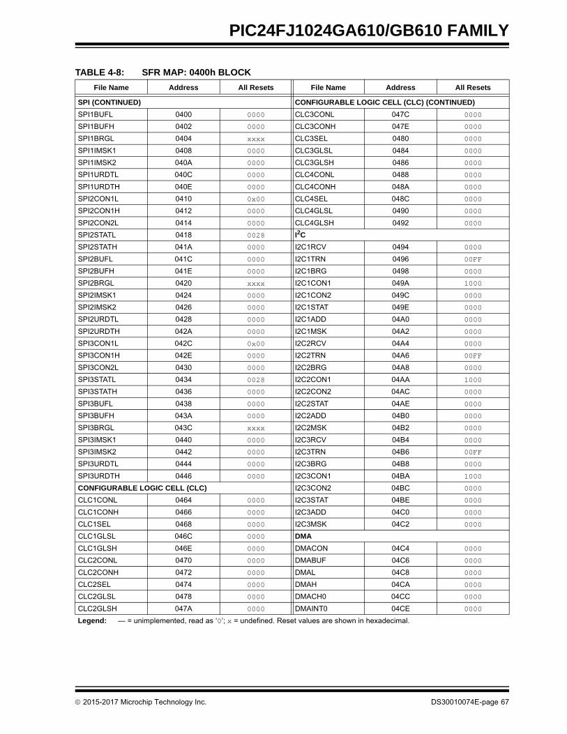
PIC24FJ1024GA610/GB610 FAMILY
TABLE 4-8: SFR MAP: 0400h BLOCK
File Name Address All Resets File Name Address All Resets
SPI (CONTINUED) CONFIGURABLE LOGIC CELL (CLC) (CONTINUED)
SPI1BUFL 0400 0000 CLC3CONL 047C 0000
SPI1BUFH 0402 0000 CLC3CONH 047E 0000
SPI1BRGL 0404 xxxx CLC3SEL 0480 0000
SPI1IMSK1 0408 0000 CLC3GLSL 0484 0000
SPI1IMSK2 040A 0000 CLC3GLSH 0486 0000
SPI1URDTL 040C 0000 CLC4CONL 0488 0000
SPI1URDTH 040E 0000 CLC4CONH 048A 0000
SPI2CON1L 0410 0x00 CLC4SEL 048C 0000
SPI2CON1H 0412 0000 CLC4GLSL 0490 0000
SPI2CON2L 0414 0000 CLC4GLSH 0492 0000
SPI2STATL 0418 0028 I2C
SPI2STATH 041A 0000 I2C1RCV 0494 0000
SPI2BUFL 041C 0000 I2C1TRN 0496 00FF
SPI2BUFH 041E 0000 I2C1BRG 0498 0000
SPI2BRGL 0420 xxxx I2C1CON1 049A 1000
SPI2IMSK1 0424 0000 I2C1CON2 049C 0000
SPI2IMSK2 0426 0000 I2C1STAT 049E 0000
SPI2URDTL 0428 0000 I2C1ADD 04A0 0000
SPI2URDTH 042A 0000 I2C1MSK 04A2 0000
SPI3CON1L 042C 0x00 I2C2RCV 04A4 0000
SPI3CON1H 042E 0000 I2C2TRN 04A6 00FF
SPI3CON2L 0430 0000 I2C2BRG 04A8 0000
SPI3STATL 0434 0028 I2C2CON1 04AA 1000
SPI3STATH 0436 0000 I2C2CON2 04AC 0000
SPI3BUFL 0438 0000 I2C2STAT 04AE 0000
SPI3BUFH 043A 0000 I2C2ADD 04B0 0000
SPI3BRGL 043C xxxx I2C2MSK 04B2 0000
SPI3IMSK1 0440 0000 I2C3RCV 04B4 0000
SPI3IMSK2 0442 0000 I2C3TRN 04B6 00FF
SPI3URDTL 0444 0000 I2C3BRG 04B8 0000
SPI3URDTH 0446 0000 I2C3CON1 04BA 1000
CONFIGURABLE LOGIC CELL (CLC) I2C3CON2 04BC 0000
CLC1CONL 0464 0000 I2C3STAT 04BE 0000
CLC1CONH 0466 0000 I2C3ADD 04C0 0000
CLC1SEL 0468 0000 I2C3MSK 04C2 0000
CLC1GLSL 046C 0000 DMA
CLC1GLSH 046E 0000 DMACON 04C4 0000
CLC2CONL 0470 0000 DMABUF 04C6 0000
CLC2CONH 0472 0000 DMAL 04C8 0000
CLC2SEL 0474 0000 DMAH 04CA 0000
CLC2GLSL 0478 0000 DMACH0 04CC 0000
CLC2GLSH 047A 0000 DMAINT0 04CE 0000
Legend: — = unimplemented, read as ‘0’; x = undefined. Reset values are shown in hexadecimal.
2015-2017 Microchip Technology Inc. DS30010074E-page 67
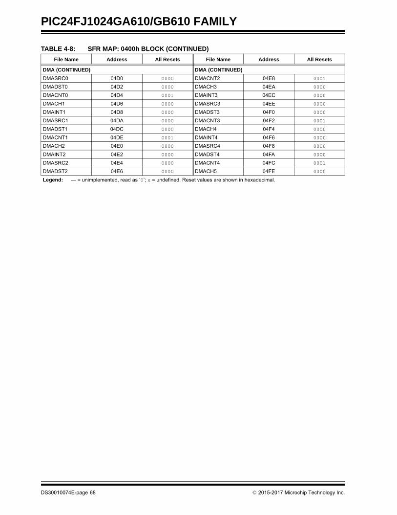
PIC24FJ1024GA610/GB610 FAMILY
DMA (CONTINUED) DMA (CONTINUED)
DMASRC0 04D0 0000 DMACNT2 04E8 0001
DMADST0 04D2 0000 DMACH3 04EA 0000
DMACNT0 04D4 0001 DMAINT3 04EC 0000
DMACH1 04D6 0000 DMASRC3 04EE 0000
DMAINT1 04D8 0000 DMADST3 04F0 0000
DMASRC1 04DA 0000 DMACNT3 04F2 0001
DMADST1 04DC 0000 DMACH4 04F4 0000
DMACNT1 04DE 0001 DMAINT4 04F6 0000
DMACH2 04E0 0000 DMASRC4 04F8 0000
DMAINT2 04E2 0000 DMADST4 04FA 0000
DMASRC2 04E4 0000 DMACNT4 04FC 0001
DMADST2 04E6 0000 DMACH5 04FE 0000
TABLE 4-8: SFR MAP: 0400h BLOCK (CONTINUED)
File Name Address All Resets File Name Address All Resets
Legend: — = unimplemented, read as ‘0’; x = undefined. Reset values are shown in hexadecimal.
DS30010074E-page 68 2015-2017 Microchip Technology Inc.

PIC24FJ1024GA610/GB610 FAMILY
TABLE 4-9: SFR MAP: 0500h BLOCK
File Name Address All Resets File Name Address All Resets
DMA (CONTINUED) USB OTG (CONTINUED)
DMAINT5 0500 0000 U1ADDR 056E 00xx
DMASRC5 0502 0000 U1BDTP1 0570 0000
DMADST5 0504 0000 U1FRML 0572 0000
DMACNT5 0506 0001 U1FRMH 0574 0000
DMACH6 0508 0000 U1TOK 0576 0000
DMAINT6 050A 0000 U1SOF 0578 0000
DMASRC6 050C 0000 U1BDTP2 057A 0000
DMADST6 050E 0000 U1BDTP3 057C 0000
DMACNT6 0510 0001 U1CNFG1 057E 0000
DMACH7 0512 0000 U1CNFG2 0580 0000
DMAINT7 0514 0000 U1EP0 0582 0000
DMASRC7 0516 0000 U1EP1 0584 0000
DMADST7 0518 0000 U1EP2 0586 0000
DMACNT7 051A 0001 U1EP3 0588 0000
USB OTG U1EP4 058A 0000
U1OTGIR 0558 0000 U1EP5 058C 0000
U1OTGIE 055A 0000 U1EP6 058E 0000
U1OTGSTAT 055C 0000 U1EP7 0590 0000
U1OTGCON 055E 0000 U1EP8 0592 0000
U1PWRC 0560 00x0 U1EP9 0594 0000
U1IR 0562 0000 U1EP10 0596 0000
U1IE 0564 0000 U1EP11 0598 0000
U1EIR 0566 0000 U1EP12 059A 0000
U1EIE 0568 0000 U1EP13 059C 0000
U1STAT 056A 0000 U1EP14 059E 0000
U1CON 056C 00x0 U1EP15 05A0 0000
Legend: — = unimplemented, read as ‘0’; x = undefined. Reset values are shown in hexadecimal.
2015-2017 Microchip Technology Inc. DS30010074E-page 69

PIC24FJ1024GA610/GB610 FAMILY
TABLE 4-10: SFR MAP: 0600h BLOCK
File Name Address All Resets File Name Address All Resets
I/O PORTD (CONTINUED)
PADCON 065E 0000 ANSD 06A6 FFFF
IOCSTAT 0660 0000 IOCPD 06A8 0000
PORTA(1) IOCND 06AA 0000
TRISA 0662 FFFF IOCFD 06AC 0000
PORTA 0664 0000 IOCPUD 06AE 0000
LATA 0666 0000 IOCPDD 06B0 0000
ODCA 0668 0000 PORTE
ANSA 066A FFFF TRISE 06B2 FFFF
IOCPA 066C 0000 PORTE 06B4 0000
IOCNA 066E 0000 LATE 06B6 0000
IOCFA 0670 0000 ODCE 06B8 0000
IOCPUA 0672 0000 ANSE 06BA FFFF
IOCPDA 0674 0000 IOCPE 06BC 0000
PORTB IOCNE 06BE 0000
TRISB 0676 FFFF IOCFE 06C0 0000
PORTB 0678 0000 IOCPUE 06C2 0000
LATB 067A 0000 IOCPDE 06C4 0000
ODCB 067C 0000 PORTF
ANSB 067E FFFF TRISF 06C6 FFFF
IOCPB 0680 0000 PORTF 06C8 0000
IOCNB 0682 0000 LATF 06CA 0000
IOCFB 0684 0000 ODCF 06CC 0000
IOCPUB 0686 0000 IOCPF 06D0 0000
IOCPDB 0688 0000 IOCNF 06D2 0000
PORTC IOCFF 06D4 0000
TRISC 068A FFFF IOCPUF 06D6 0000
PORTC 068C 0000 IOCPDF 06D8 0000
LATC 068E 0000 PORTG
ODCC 0690 0000 TRISG 06DA FFFF
ANSC 0692 FFFF PORTG 06DC 0000
IOCPC 0694 0000 LATG 06DE 0000
IOCNC 0696 0000 ODCG 06E0 0000
IOCFC 0698 0000 ANSG 06E2 FFFF
IOCPUC 069A 0000 IOCPG 06E4 0000
IOCPDC 069C 0000 IOCNG 06E6 0000
PORTD IOCFG 06E8 0000
TRISD 069E FFFF IOCPUG 06EA 0000
PORTD 06A0 0000 IOCPDG 06EC 0000
LATD 06A2 0000
ODCD 06A4 0000
Legend: — = unimplemented, read as ‘0’; x = undefined. Reset values are shown in hexadecimal.
Note 1: PORTA and all associated bits are unimplemented in 64-pin devices and read as ‘0’.
DS30010074E-page 70 2015-2017 Microchip Technology Inc.

PIC24FJ1024GA610/GB610 FAMILY
TABLE 4-11: SFR MAP: 0700h BLOCK
File Name Address All Resets File Name Address All Resets
A/D PERIPHERAL PIN SELECT
ADC1BUF0 0712 xxxx RPINR0 0790 3F3F
ADC1BUF1 0714 xxxx RPINR1 0792 3F3F
ADC1BUF2 0716 xxxx RPINR2 0794 3F3F
ADC1BUF3 0718 xxxx RPINR3 0796 3F3F
ADC1BUF4 071A xxxx RPINR4 0798 3F3F
ADC1BUF5 071C xxxx RPINR5 079A 3F3F
ADC1BUF6 071E xxxx RPINR6 079C 3F3F
ADC1BUF7 0720 xxxx RPINR7 079E 3F3F
ADC1BUF8 0722 xxxx RPINR8 07A0 003F
ADC1BUF9 0724 xxxx RPINR11 07A6 3F3F
ADC1BUF10 0726 xxxx RPINR12 07A8 3F3F
ADC1BUF11 0728 xxxx RPINR14 07AC 3F3F
ADC1BUF12 072A xxxx RPINR15 07AE 003F
ADC1BUF13 072C xxxx RPINR17 07B2 3F00
ADC1BUF14 072E xxxx RPINR18 07B4 3F3F
ADC1BUF15 0730 xxxx RPINR19 07B6 3F3F
ADC1BUF16 0732 xxxx RPINR20 07B8 3F3F
ADC1BUF17 0734 xxxx RPINR21 07BA 3F3F
ADC1BUF18 0736 xxxx RPINR22 07BC 3F3F
ADC1BUF19 0738 xxxx RPINR23 07BE 3F3F
ADC1BUF20 073A xxxx RPINR25 07C2 3F3F
ADC1BUF21 073C xxxx RPINR27 07C6 3F3F
ADC1BUF22 073E xxxx RPINR28 07C8 3F3F
ADC1BUF23 0740 xxxx RPINR29 07CA 003F
ADC1BUF24 0742 xxxx RPOR0 07D4 0000
ADC1BUF25 0744 xxxx RPOR1 07D6 0000
AD1CON1 0746 0000 RPOR2 07D8 0000
AD1CON2 0748 0000 RPOR3 07DA 0000
AD1CON3 074A 0000 RPOR4 07DC 0000
AD1CHS 074C 0000 RPOR5 07DE 0000
AD1CSSH 074E 0000 RPOR6 07E0 0000
AD1CSSL 0750 0000 RPOR7 07E2 0000
AD1CON4 0752 0000 RPOR8 07E4 0000
AD1CON5 0754 0000 RPOR9 07E6 0000
AD1CHITH 0756 0000 RPOR10 07E8 0000
AD1CHITL 0758 0000 RPOR11 07EA 0000
AD1CTMENH 075A 0000 RPOR12 07EC 0000
AD1CTMENL 075C 0000 RPOR13 07EE 0000
AD1RESDMA 075E 0000 RPOR14 07F0 0000
NVM RPOR15 07F2 0000
NVMCON 0760 0000
NVMADR 0762 xxxx
NVMADRU 0764 00xx
NVMKEY 0766 0000
Legend: — = unimplemented, read as ‘0’; x = undefined. Reset values are shown in hexadecimal.
2015-2017 Microchip Technology Inc. DS30010074E-page 71

PIC24FJ1024GA610/GB610 FAMILY
4.2.5 EXTENDED DATA SPACE (EDS)
The Extended Data Space (EDS) allows PIC24Fdevices to address a much larger range of data thanwould otherwise be possible with a 16-bit addressrange. EDS includes any additional internal datamemory not directly accessible by the lower 32-Kbytedata address space and any external memory throughEPMP.
In addition, EDS also allows read access to theprogram memory space. This feature is called ProgramSpace Visibility (PSV) and is discussed in detail inSection 4.3.3 “Reading Data from Program MemoryUsing EDS”.
Figure 4-4 displays the entire EDS space. The EDS isorganized as pages, called EDS pages, with one pageequal to the size of the EDS window (32 Kbytes). A par-ticular EDS page is selected through the Data SpaceRead Page register (DSRPAG) or the Data Space WritePage register (DSWPAG). For PSV, only the DSRPAGregister is used. The combination of the DSRPAGregister value and the 16-bit wide data address forms a24-bit Effective Address (EA).
The data addressing range of the PIC24FJ1024GA610/GB610 family devices depends on the version of theEnhanced Parallel Master Port implemented on a partic-ular device; this is, in turn, a function of device pin count.Table 4-12 lists the total memory accessible by each ofthe devices in this family. For more details on accessingexternal memory using EPMP, refer to the “dsPIC33/PIC24 Family Reference Manual”, “Enhanced ParallelMaster Port (EPMP)” (DS39730).
.
FIGURE 4-4: EXTENDED DATA SPACE
TABLE 4-12: TOTAL ACCESSIBLE DATA MEMORY
FamilyInternal
RAM
External RAM Access Using
EPMP
PIC24FJXXXGX610 32K Up to 16 Mbytes
PIC24FJXXXGX606 32K Up to 64K
Note: Accessing Page 0 in the EDS window willgenerate an address error trap as Page 0is the base data memory (data locations,0800h to 7FFFh, in the lower Data Space).
0000hSpecial
Registers
32-KbyteEDS
8000h
Program Memory
DSxPAG= 002h
DSxPAG= 1FFh
DSRPAG= 200h
DSRPAG= 3FFh
Function
018000h
01FFFEh
000000h 7F8001h
FFFFFEh 007FFEh 7FFFFFh
ProgramSpace
0800h
FFFEh
EDS Pages
EPMP Memory Space(1)
ExternalMemoryAccessUsing
EPMP(1)
FF8000h
DSRPAG= 2FFh
7F8000h
7FFFFEh
Access
ProgramSpaceAccess
ProgramSpaceAccess
DSRPAG= 300h
000001h
007FFFh
ProgramSpaceAccess
Note 1: The range of addressable memory available is dependent on the device pin count and EPMP implementation.
ExternalMemoryAccessUsing
EPMP(1)
InternalData
MemorySpace
(up to30 Kbytes)
(LowerWord)
(LowerWord)
(UpperWord)
(UpperWord)
Window
DSxPAG= 001h
008000h
008800h
InternalData
MemorySpace
2 Kbytes
DS30010074E-page 72 2015-2017 Microchip Technology Inc.

PIC24FJ1024GA610/GB610 FAMILY
4.2.5.1 Data Read from EDS
In order to read the data from the EDS space, first, anAddress Pointer is set up by loading the required EDSpage number into the DSRPAG register and assigningthe offset address to one of the W registers. Once theabove assignment is done, the EDS window is enabledby setting bit 15 of the Working register which isassigned with the offset address; then, the contents ofthe pointed EDS location can be read.
Figure 4-5 illustrates how the EDS space address isgenerated for read operations.
When the Most Significant bit (MSb) of EA is ‘1’ andDSRPAG<9> = 0, the lower 9 bits of DSRPAG are con-catenated to the lower 15 bits of EA to form a 24-bitEDS space address for read operations.
Example 4-1 shows how to read a byte, word anddouble word from EDS.
FIGURE 4-5: EDS ADDRESS GENERATION FOR READ OPERATIONS
EXAMPLE 4-1: EDS READ CODE IN ASSEMBLY
Note: All read operations from EDS space havean overhead of one instruction cycle.Therefore, a minimum of two instructioncycles are required to complete an EDSread. For EDS reads under the REPEATinstruction; the first two accesses takethree cycles and the subsequentaccesses take one cycle.
DSRPAG Reg
SelectWn
9 8
15 Bits9 Bits
24-Bit EA
Wn<0> is Byte Select0 = Extended SRAM and EPMP
1
0
; Set the EDS page from where the data to be readmov #0x0002, w0mov w0, DSRPAG ;page 2 is selected for readmov #0x0800, w1 ;select the location (0x800) to be readbset w1, #15 ;set the MSB of the base address, enable EDS mode
;Read a byte from the selected locationmov.b [w1++], w2 ;read Low bytemov.b [w1++], w3 ;read High byte
;Read a word from the selected locationmov [w1], w2 ;
;Read Double - word from the selected locationmov.d [w1], w2 ;two word read, stored in w2 and w3
2015-2017 Microchip Technology Inc. DS30010074E-page 73

PIC24FJ1024GA610/GB610 FAMILY
4.2.5.2 Data Write into EDS
In order to write data to EDS, such as in EDS reads, anAddress Pointer is set up by loading the required EDSpage number into the DSWPAG register and assigningthe offset address to one of the W registers. Once theabove assignment is done, then the EDS window isenabled by setting bit 15 of the Working register,assigned with the offset address and the accessedlocation can be written.
Figure 4-2 illustrates how the EDS address is generatedfor write operations.
When the MSbs of EA are ‘1’, the lower 9 bits ofDSWPAG are concatenated to the lower 15 bits of EAto form a 24-bit EDS address for write operations.Example 4-2 shows how to write a byte, word anddouble word to EDS.
The Data Space Page registers (DSRPAG/DSWPAG)do not update automatically while crossing a pageboundary when the rollover happens from 0xFFFF to
0x8000. While developing code in assembly, care mustbe taken to update the Data Space Page registers whenan Address Pointer crosses the page boundary. The ‘C’compiler keeps track of the addressing, and incrementsor decrements the Page registers accordingly, whileaccessing contiguous data memory locations.
FIGURE 4-6: EDS ADDRESS GENERATION FOR WRITE OPERATIONS
EXAMPLE 4-2: EDS WRITE CODE IN ASSEMBLY
Note 1: All write operations to EDS are executedin a single cycle.
2: Use of Read/Modify/Write operation onany EDS location under a REPEATinstruction is not supported. For example,BCLR, BSW, BTG, RLC f, RLNC f, RRC f,RRNC f, ADD f, SUB f, SUBR f, AND f,IOR f, XOR f, ASR f, ASL f.
3: Use the DSRPAG register whileperforming Read/Modify/Write operations.
DSWPAG Reg
SelectWn
8
15 Bits9 Bits
24-Bit EA
Wn<0> is Byte Select
1
0
; Set the EDS page where the data to be writtenmov #0x0002, w0mov w0, DSWPAG ;page 2 is selected for writemov #0x0800, w1 ;select the location (0x800) to be writtenbset w1, #15 ;set the MSB of the base address, enable EDS mode
;Write a byte to the selected locationmov #0x00A5, w2mov #0x003C, w3mov.b w2, [w1++] ;write Low bytemov.b w3, [w1++] ;write High byte
;Write a word to the selected locationmov #0x1234, w2 ;mov w2, [w1] ;
;Write a Double - word to the selected locationmov #0x1122, w2mov #0x4455, w3mov.d w2, [w1] ;2 EDS writes
DS30010074E-page 74 2015-2017 Microchip Technology Inc.

PIC24FJ1024GA610/GB610 FAMILY
TABLE 4-13: EDS MEMORY ADDRESS WITH DIFFERENT PAGES AND ADDRESSES
4.2.6 SOFTWARE STACK
Apart from its use as a Working register, the W15register in PIC24F devices is also used as a SoftwareStack Pointer (SSP). The pointer always points to thefirst available free word and grows from lower to higheraddresses. It pre-decrements for stack pops and post-increments for stack pushes, as shown in Figure 4-7.Note that for a PC push during any CALL instruction,the MSB of the PC is zero-extended before the push,ensuring that the MSB is always clear.
The Stack Pointer Limit Value register (SPLIM), associ-ated with the Stack Pointer, sets an upper addressboundary for the stack. SPLIM is uninitialized at Reset.As is the case for the Stack Pointer, SPLIM<0> isforced to ‘0’ as all stack operations must be word-aligned. Whenever an EA is generated using W15 as asource or destination pointer, the resulting address iscompared with the value in SPLIM. If the contents ofthe Stack Pointer (W15) and the SPLIM register areequal, and a push operation is performed, a stack errortrap will not occur. The stack error trap will occur on asubsequent push operation. Thus, for example, if it is
desirable to cause a stack error trap when the stackgrows beyond address 2000h in RAM, initialize theSPLIM with the value, 1FFEh.
Similarly, a Stack Pointer underflow (stack error) trap isgenerated when the Stack Pointer address is found tobe less than 0800h. This prevents the stack frominterfering with the SFR space.
A write to the SPLIM register should not be immediatelyfollowed by an indirect read operation using W15.
FIGURE 4-7: CALL STACK FRAME
DSRPAG(Data Space Read
Register)
DSWPAG (Data Space Write
Register)
Source/Destination Address while
Indirect Addressing
24-Bit EA Pointing to EDS
Comment
x(1) x(1) 0000h to 1FFFh 000000h to 001FFFh
Near Data Space(2)
2000h to 7FFFh 002000h to 007FFFh
001h 001h
8000h to FFFFh
008000h to 00FFFEh
EPMP Memory Space
002h 002h 010000h to 017FFEh
003h
•
•
•
•
•
1FFh
003h
•
•
•
•
•
1FFh
018000h to 0187FEh
•
•
•
•
FF8000h to FFFFFEh
000h 000h Invalid Address Address Error Trap(3)
Note 1: If the source/destination address is below 8000h, the DSRPAG and DSWPAG registers are not considered.
2: This Data Space can also be accessed by Direct Addressing.
3: When the source/destination address is above 8000h and DSRPAG/DSWPAG are ‘0’, an address error trap will occur.
Note: A PC push during exception processingwill concatenate the SRL register to theMSB of the PC prior to the push.
<Free Word>
PC<15:0>
000000000
015
W15 (before CALL)
W15 (after CALL)
Sta
ck G
row
s To
wa
rds
Hig
her
Ad
dre
ss
0000h
PC<22:16>
POP : [--W15]PUSH : [W15++]
2015-2017 Microchip Technology Inc. DS30010074E-page 75

PIC24FJ1024GA610/GB610 FAMILY
4.3 Interfacing Program and Data Memory Spaces
The PIC24F architecture uses a 24-bit wide programspace and 16-bit wide Data Space. The architecture isalso a modified Harvard scheme, meaning that datacan also be present in the program space. To use thisdata successfully, it must be accessed in a way thatpreserves the alignment of information in both spaces.
Aside from normal execution, the PIC24F architectureprovides two methods by which program space can beaccessed during operation:
• Using table instructions to access individual bytes or words anywhere in the program space
• Remapping a portion of the program space into the Data Space (Program Space Visibility)
Table instructions allow an application to read or writeto small areas of the program memory. This makes themethod ideal for accessing data tables that need to beupdated from time to time. It also allows access to allbytes of the program word. The remapping methodallows an application to access a large block of data ona read-only basis, which is ideal for look-ups from alarge table of static data. It can only access the leastsignificant word of the program word.
4.3.1 ADDRESSING PROGRAM SPACE
Since the address ranges for the data and programspaces are 16 and 24 bits, respectively, a method isneeded to create a 23-bit or 24-bit program addressfrom 16-bit data registers. The solution depends on theinterface method to be used.
For table operations, the 8-bit Table Memory PageAddress register (TBLPAG) is used to define a 32K wordregion within the program space. This is concatenatedwith a 16-bit EA to arrive at a full 24-bit program spaceaddress. In this format, the MSBs of TBLPAG are usedto determine if the operation occurs in the usermemory (TBLPAG<7> = 0) or the configuration memory(TBLPAG<7> = 1).
For remapping operations, the 10-bit Extended DataSpace Read register (DSRPAG) is used to define a16K word page in the program space. When the MostSignificant bit (MSb) of the EA is ‘1’, and the MSb (bit 9)of DSRPAG is ‘1’, the lower 8 bits of DSRPAG areconcatenated with the lower 15 bits of the EA to form a23-bit program space address. The DSRPAG<8> bitdecides whether the lower word (when bit is ‘0’) or thehigher word (when bit is ‘1’) of program memory ismapped. Unlike table operations, this strictly limitsremapping operations to the user memory area.
Table 4-14 and Figure 4-8 show how the program EA iscreated for table operations and remapping accessesfrom the data EA. Here, P<23:0> refers to a programspace word, whereas D<15:0> refers to a Data Spaceword.
TABLE 4-14: PROGRAM SPACE ADDRESS CONSTRUCTION
Access TypeAccessSpace
Program Space Address
<23> <22:16> <15> <14:1> <0>
Instruction Access(Code Execution)
User 0 PC<22:1> 0
0xx xxxx xxxx xxxx xxxx xxx0
TBLRD/TBLWT(Byte/Word Read/Write)
User TBLPAG<7:0> Data EA<15:0>
0xxx xxxx xxxx xxxx xxxx xxxx
Configuration TBLPAG<7:0> Data EA<15:0>
1xxx xxxx xxxx xxxx xxxx xxxx
Program Space Visibility(Block Remap/Read)
User 0 DSRPAG<7:0>(2) Data EA<14:0>(1)
0 xxxx xxxx xxx xxxx xxxx xxxx
Note 1: Data EA<15> is always ‘1’ in this case, but is not used in calculating the program space address. Bit 15 of the address is DSRPAG<0>.
2: DSRPAG<9> is always ‘1’ in this case. DSRPAG<8> decides whether the lower word or higher word of program memory is read. When DSRPAG<8> is ‘0’, the lower word is read, and when it is ‘1’, the higher word is read.
DS30010074E-page 76 2015-2017 Microchip Technology Inc.
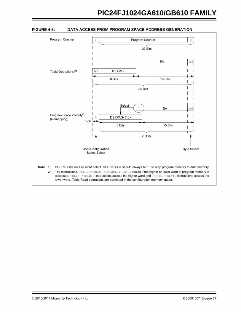
PIC24FJ1024GA610/GB610 FAMILY
FIGURE 4-8: DATA ACCESS FROM PROGRAM SPACE ADDRESS GENERATION
0Program Counter
23 Bits
1
DSRPAG<7:0>
8 Bits
EA
15 Bits
Program Counter
Select
TBLPAG
8 Bits
EA
16 Bits
Byte Select
0
0
1/0
User/Configuration
Table Operations(2)
Program Space Visibility(1)
Space Select
24 Bits
23 Bits
(Remapping)
1/0
1/0
Note 1: DSRPAG<8> acts as word select. DSRPAG<9> should always be ‘1’ to map program memory to data memory.
2: The instructions, TBLRDH/TBLWTH/TBLRDL/TBLWTL, decide if the higher or lower word of program memory is accessed. TBLRDH/TBLWTH instructions access the higher word and TBLRDL/TBLWTL instructions access the lower word. Table Read operations are permitted in the configuration memory space.
1-Bit
2015-2017 Microchip Technology Inc. DS30010074E-page 77

PIC24FJ1024GA610/GB610 FAMILY
4.3.2 DATA ACCESS FROM PROGRAM MEMORY USING TABLE INSTRUCTIONS
The TBLRDL and TBLWTL instructions offer a directmethod of reading or writing the lower word of anyaddress within the program space without going throughData Space. The TBLRDH and TBLWTH instructions arethe only method to read or write the upper 8 bits of aprogram space word as data.
The PC is incremented by two for each successive24-bit program word. This allows program memoryaddresses to directly map to Data Space addresses.Program memory can thus be regarded as two, 16-bitword-wide address spaces, residing side by side, eachwith the same address range. TBLRDL and TBLWTLaccess the space which contains the least significantdata word, and TBLRDH and TBLWTH access the spacewhich contains the upper data byte.
Two table instructions are provided to move byte orword-sized (16-bit) data to and from program space.Both function as either byte or word operations.
1. TBLRDL (Table Read Low): In Word mode, itmaps the lower word of the program spacelocation (P<15:0>) to a data address (D<15:0>).
In Byte mode, either the upper or lower byte ofthe lower program word is mapped to the lowerbyte of a data address. The upper byte isselected when byte select is ‘1’; the lower byteis selected when it is ‘0’.
2. TBLRDH (Table Read High): In Word mode, itmaps the entire upper word of a program address(P<23:16>) to a data address. Note thatD<15:8>, the ‘phantom’ byte, will always be ‘0’.
In Byte mode, it maps the upper or lower byte ofthe program word to D<7:0> of the dataaddress, as above. Note that the data willalways be ‘0’ when the upper ‘phantom’ byte isselected (byte select = 1).
In a similar fashion, two table instructions, TBLWTHand TBLWTL, are used to write individual bytes orwords to a program space address. The details oftheir operation are described in Section 6.0 “FlashProgram Memory”.
For all table operations, the area of program memoryspace to be accessed is determined by the TableMemory Page Address register (TBLPAG). TBLPAGcovers the entire program memory space of thedevice, including user and configuration spaces. WhenTBLPAG<7> = 0, the table page is located in the usermemory space. When TBLPAG<7> = 1, the page islocated in configuration space.
FIGURE 4-9: ACCESSING PROGRAM MEMORY WITH TABLE INSTRUCTIONS
Note: Only Table Read operations will executein the configuration memory space whereDevice IDs are located. Table Writeoperations are not allowed.
081623
0000000000000000
0000000000000000
‘Phantom’ Byte
TBLRDH.B (Wn<0> = 0)
TBLRDL.W
TBLRDL.B (Wn<0> = 1)
TBLRDL.B (Wn<0> = 0)
23 15 0
TBLPAG02
000000h
800000h
020000h
030000h
Program Space
Data EA<15:0>
The address for the table operation is determined by the data EAwithin the page defined by the TBLPAG register. Only read operations are shown; write operations are also valid inthe user memory area.
DS30010074E-page 78 2015-2017 Microchip Technology Inc.

PIC24FJ1024GA610/GB610 FAMILY
4.3.3 READING DATA FROM PROGRAM MEMORY USING EDS
The upper 32 Kbytes of Data Space may optionally bemapped into any 16K word page of the program space.This provides transparent access of stored constantdata from the Data Space without the need to usespecial instructions (i.e., TBLRDL/H).
Program space access through the Data Space occurswhen the MSb of EA is ‘1’ and the DSRPAG<9> is also‘1’. The lower 8 bits of DSRPAG are concatenated tothe Wn<14:0> bits to form a 23-bit EA to access pro-gram memory. The DSRPAG<8> decides which wordshould be addressed; when the bit is ‘0’, the lowerword, and when ‘1’, the upper word of the programmemory is accessed.
The entire program memory is divided into 512 EDSpages, from 200h to 3FFh, each consisting of 16K wordsof data. Pages, 200h to 2FFh, correspond to the lowerwords of the program memory, while 300h to 3FFhcorrespond to the upper words of the program memory.
Using this EDS technique, the entire program memorycan be accessed. Previously, the access to the upperword of the program memory was not supported.
Table 4-15 provides the corresponding 23-bit EDSaddress for program memory with EDS page andsource addresses.
For operations that use PSV and are executed outside aREPEAT loop, the MOV and MOV.D instructions will requireone instruction cycle in addition to the specified executiontime. All other instructions will require two instructioncycles in addition to the specified execution time.
For operations that use PSV, which are executed insidea REPEAT loop, there will be some instances thatrequire two instruction cycles in addition to thespecified execution time of the instruction:
• Execution in the first iteration
• Execution in the last iteration
• Execution prior to exiting the loop due to an interrupt
• Execution upon re-entering the loop after an interrupt is serviced
Any other iteration of the REPEAT loop will allow theinstruction accessing data, using PSV, to execute in asingle cycle.
TABLE 4-15: EDS PROGRAM ADDRESS WITH DIFFERENT PAGES AND ADDRESSES
EXAMPLE 4-3: EDS READ CODE FROM PROGRAM MEMORY IN ASSEMBLY
DSRPAG (Data Space Read Register)
Source Address while Indirect Addressing
23-Bit EA Pointing to EDS
Comment
200h•••
2FFh
8000h to FFFFh
000000h to 007FFEh•••
7F8000h to 7FFFFEh
Lower words of 4M program instructions; (8 Mbytes) for read operations only.
300h•••
3FFh
000001h to 007FFFh•••
7F8001h to 7FFFFFh
Upper words of 4M program instructions (4 Mbytes remaining; 4 Mbytes are phantom bytes) for read operations only.
000h Invalid Address Address error trap.(1)
Note 1: When the source/destination address is above 8000h and DSRPAG/DSWPAG is ‘0’, an address error trap will occur.
; Set the EDS page from where the data to be readmov #0x0202, w0mov w0, DSRPAG ;page 0x202, consisting lower words, is selected for readmov #0x000A, w1 ;select the location (0x0A) to be readbset w1, #15 ;set the MSB of the base address, enable EDS mode
;Read a byte from the selected locationmov.b [w1++], w2 ;read Low bytemov.b [w1++], w3 ;read High byte
;Read a word from the selected locationmov [w1], w2 ;
;Read Double - word from the selected locationmov.d [w1], w2 ;two word read, stored in w2 and w3
2015-2017 Microchip Technology Inc. DS30010074E-page 79

PIC24FJ1024GA610/GB610 FAMILY
FIGURE 4-10: PROGRAM SPACE VISIBILITY OPERATION TO ACCESS LOWER WORD
FIGURE 4-11: PROGRAM SPACE VISIBILITY OPERATION TO ACCESS UPPER WORD
23 15 0DSRPAGData SpaceProgram Space
0000h
8000h
FFFFh
202h000000h
7FFFFEh
010000h
017FFEh
When DSRPAG<9:8> = 10 and EA<15> = 1
EDS Window
The data in the page designated by DSRPAG is mapped into the upper half of the data memory space....
Data EA<14:0>
...while the lower 15 bits of the EA specify an exact address within the EDS area. This corre-sponds exactly to the same lower 15 bits of the actual program space address.
23 15 0DSRPAGData SpaceProgram Space
0000h
8000h
FFFFh
302h000000h
7FFFFEh
010001h
017FFFh
When DSRPAG<9:8> = 11 and EA<15> = 1
The data in the page designated by DSRPAG is mapped into the upper half of the data memory space....
Data EA<14:0>
...while the lower 15 bits of the EA specify an exact address within the EDS area. This corre-sponds exactly to the same lower 15 bits of the actual program space address.
EDS Window
DS30010074E-page 80 2015-2017 Microchip Technology Inc.

PIC24FJ1024GA610/GB610 FAMILY
5.0 DIRECT MEMORY ACCESS CONTROLLER (DMA)
The Direct Memory Access Controller (DMA) is designedto service high-throughput data peripherals operating onthe SFR bus, allowing them to access data memorydirectly and alleviating the need for CPU intensive man-agement. By allowing these data intensive peripherals toshare their own data path, the main data bus is alsodeloaded, resulting in additional power savings.
The DMA Controller functions both as a peripheral anda direct extension of the CPU. It is located on themicrocontroller data bus between the CPU and DMA-enabled peripherals, with direct access to SRAM. Thispartitions the SFR bus into two buses, allowing theDMA Controller access to the DMA capable peripheralslocated on the new DMA SFR bus. The controllerserves as a master device on the DMA SFR bus,controlling data flow from DMA capable peripherals.
The controller also monitors CPU instruction process-ing directly, allowing it to be aware of when the CPUrequires access to peripherals on the DMA bus andautomatically relinquishing control to the CPU asneeded. This increases the effective bandwidth forhandling data without DMA operations causing aprocessor stall. This makes the controller essentiallytransparent to the user.
The DMA Controller has these features:
• Eight Multiple Independent and Independently Programmable Channels
• Concurrent Operation with the CPU (no DMA caused Wait states)
• DMA Bus Arbitration
• Five Programmable Address modes
• Four Programmable Transfer modes
• Four Flexible Internal Data Transfer modes
• Byte or Word Support for Data Transfer
• 16-Bit Source and Destination Address Register for Each Channel, Dynamically Updated and Reloadable
• 16-Bit Transaction Count Register, Dynamically Updated and Reloadable
• Upper and Lower Address Limit Registers
• Counter Half-Full Level Interrupt
• Software Triggered Transfer
• Null Write mode for Symmetric Buffer Operations
A simplified block diagram of the DMA Controller isshown in Figure 5-1.
FIGURE 5-1: DMA FUNCTIONAL BLOCK DIAGRAM
Note: This data sheet summarizes the featuresof the PIC24FJ1024GA610/GB610 familyof devices. It is not intended to be acomprehensive reference source. To com-plement the information in this data sheet,refer to the “dsPIC33/PIC24 Family Refer-ence Manual”, “Direct Memory AccessController (DMA)” (DS39742), which isavailable from the Microchip web site(www.microchip.com). The information inthis data sheet supersedes the informationin the FRM.
To I/O Ports To DMA-EnabledPeripheralsand Peripherals
DMACH0
DMAINT0
DMASRC0
DMADST0
DMACNT0
DMACH1
DMAINT1
DMASRC1
DMADST1
DMACNT1
DMACH6
DMAINT6
DMASRC6
DMADST6
DMACNT6
DMACH7
DMAINT7
DMASRC7
DMADST7
DMACNT7
DMACON
DMAH
DMAL
DMABUF
Channel 0 Channel 1 Channel 6 Channel 7
Data RAMAddress Generation
Data RAM
Control
Logic
DataBus
CPU Execution Monitoring
2015-2017 Microchip Technology Inc. DS30010074E-page 81

PIC24FJ1024GA610/GB610 FAMILY
5.1 Summary of DMA Operations
The DMA Controller is capable of moving data betweenaddresses according to a number of different parameters.Each of these parameters can be independently config-ured for any transaction; in addition, any or all of theDMA channels can independently perform a differenttransaction at the same time. Transactions areclassified by these parameters:
• Source and destination (SFRs and data RAM)
• Data size (byte or word)
• Trigger source
• Transfer mode (One-Shot, Repeated or Continuous)
• Addressing modes (fixed address or address blocks, with or without address increment/decrement)
In addition, the DMA Controller provides channel priorityarbitration for all channels.
5.1.1 SOURCE AND DESTINATION
Using the DMA Controller, data may be moved betweenany two addresses in the Data Space. The SFR space(0000h to 07FFh), or the data RAM space (0800h toFFFFh), can serve as either the source or the destina-tion. Data can be moved between these areas in eitherdirection or between addresses in either area. The fourdifferent combinations are shown in Figure 5-2.
If it is necessary to protect areas of data RAM, the DMAController allows the user to set upper and lower addressboundaries for operations in the Data Space above theSFR space. The boundaries are set by the DMAH andDMAL Limit registers. If a DMA channel attempts anoperation outside of the address boundaries, thetransaction is terminated and an interrupt is generated.
5.1.2 DATA SIZE
The DMA Controller can handle both 8-bit and 16-bittransactions. Size is user-selectable using the SIZE bit(DMACHn<1>). By default, each channel is configuredfor word-sized transactions. When byte-sized transac-tions are chosen, the LSb of the source and/ordestination address determines if the data representsthe upper or lower byte of the data RAM location.
5.1.3 TRIGGER SOURCE
The DMA Controller can use any one of the device’sinterrupt sources to initiate a transaction. The DMATrigger sources are listed in reverse order of theirnatural interrupt priority and are shown in Table 5-1.
Since the source and destination addresses for anytransaction can be programmed independently of theTrigger source, the DMA Controller can use any Triggerto perform an operation on any peripheral. This alsoallows DMA channels to be cascaded to perform morecomplex transfer operations.
5.1.4 TRANSFER MODE
The DMA Controller supports four types of datatransfers, based on the volume of data to be moved foreach Trigger.
• One-Shot: A single transaction occurs for each Trigger.
• Continuous: A series of back-to-back transactions occur for each Trigger; the number of transactions is determined by the DMACNTn transaction counter.
• Repeated One-Shot: A single transaction is performed repeatedly, once per Trigger, until the DMA channel is disabled.
• Repeated Continuous: A series of transactions are performed repeatedly, one cycle per Trigger, until the DMA channel is disabled.
All transfer modes allow the option to have the sourceand destination addresses, and counter value automat-ically reloaded after the completion of a transaction.Repeated mode transfers do this automatically.
5.1.5 ADDRESSING MODES
The DMA Controller also supports transfers betweensingle addresses or address ranges. The four basicoptions are:
• Fixed-to-Fixed: Between two constant addresses
• Fixed-to-Block: From a constant source address to a range of destination addresses
• Block-to-Fixed: From a range of source addresses to a single, constant destination address
• Block-to-Block: From a range to source addresses to a range of destination addresses
The option to select auto-increment or auto-decrementof source and/or destination addresses is available forBlock Addressing modes.
In addition to the four basic modes, the DMA Controlleralso supports Peripheral Indirect Addressing (PIA)mode, where the source or destination address is gen-erated jointly by the DMA Controller and a PIA capableperipheral. When enabled, the DMA channel providesa base source and/or destination address, while theperipheral provides a fixed range offset address.
For PIC24FJ1024GA610/GB610 family devices, the12-bit A/D Converter module is the only PIA capableperipheral. Details for its use in PIA mode are provided inSection 25.0 “12-Bit A/D Converter with ThresholdDetect”.
DS30010074E-page 82 2015-2017 Microchip Technology Inc.
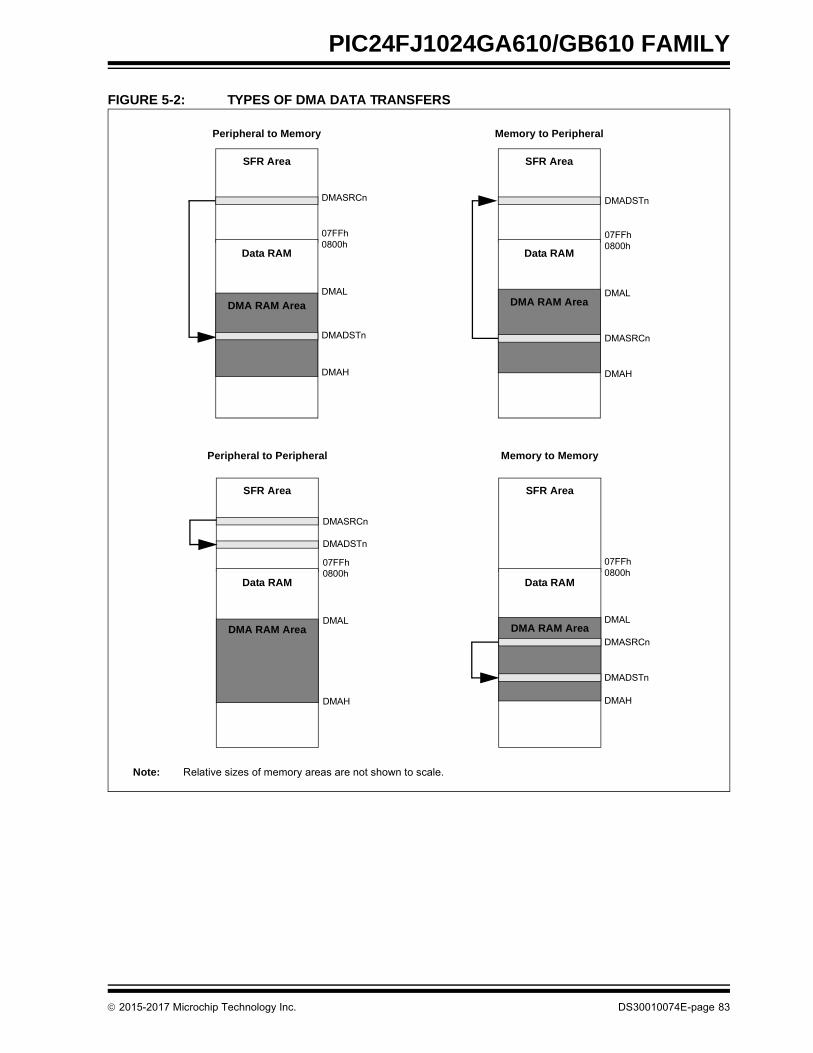
PIC24FJ1024GA610/GB610 FAMILY
FIGURE 5-2: TYPES OF DMA DATA TRANSFERS
SFR Area
Data RAM
DMA RAM Area
SFR Area
Data RAM
DMA RAM Area
SFR Area
Data RAM
SFR Area
Data RAM
07FFh0800h
DMASRCn
DMADSTn
DMA RAM AreaDMAL
DMAH
07FFh0800h
DMASRCn
DMADSTn
DMAL
DMAH
07FFh0800h
DMASRCn
DMADSTn
DMAL
DMAH
07FFh0800h
DMASRCn
DMADSTn
DMAL
DMAH
DMA RAM Area
Peripheral to Memory Memory to Peripheral
Peripheral to Peripheral Memory to Memory
Note: Relative sizes of memory areas are not shown to scale.
2015-2017 Microchip Technology Inc. DS30010074E-page 83

PIC24FJ1024GA610/GB610 FAMILY
5.1.6 CHANNEL PRIORITY
Each DMA channel functions independently of theothers, but also competes with the others for access tothe data and DMA buses. When access collisionsoccur, the DMA Controller arbitrates between thechannels using a user-selectable priority scheme. Twoschemes are available:
• Round-Robin: When two or more channels collide, the lower numbered channel receives priority on the first collision. On subsequent colli-sions, the higher numbered channels each receive priority, based on their channel number.
• Fixed: When two or more channels collide, the lowest numbered channel always receives priority, regardless of past history; however, any channel being actively processed is not available for an immediate retrigger. If a higher priority channel is continually requesting service, it will be scheduled for service after the next lower priority channel with a pending request.
5.2 Typical Setup
To set up a DMA channel for a basic data transfer:
1. Enable the DMA Controller (DMAEN = 1) andselect an appropriate channel priority schemeby setting or clearing PRSSEL.
2. Program DMAH and DMAL with the appropriateupper and lower address boundaries for dataRAM operations.
3. Select the DMA channel to be used and disableits operation (CHEN = 0).
4. Program the appropriate source and destinationaddresses for the transaction into the channel’sDMASRCn and DMADSTn registers. For PIAmode addressing, use the base address value.
5. Program the DMACNTn register for the numberof Triggers per transfer (One-Shot or Continu-ous modes) or the number of words (bytes) to betransferred (Repeated modes).
6. Set or clear the SIZE bit to select the data size.
7. Program the TRMODE<1:0> bits to select theData Transfer mode.
8. Program the SAMODE<1:0> and DAMODE<1:0>bits to select the addressing mode.
9. Enable the DMA channel by setting CHEN.
10. Enable the Trigger source interrupt.
5.3 Peripheral Module Disable
Unlike other peripheral modules, the channels of theDMA Controller cannot be individually powered downusing the Peripheral Module Disable (PMD) registers.Instead, the channels are controlled as two groups. TheDMA0MD bit (PMD7<4>) selectively controls DMACH0through DMACH3. The DMA1MD bit (PMD7<5>)controls DMACH4 through DMACH7. Setting both bitseffectively disables the DMA Controller.
5.4 Registers
The DMA Controller uses a number of registers to con-trol its operation. The number of registers depends onthe number of channels implemented for a particulardevice.
There are always four module-level registers (onecontrol and three buffer/address):
• DMACON: DMA Engine Control Register (Register 5-1)
• DMAH and DMAL: DMA High and Low Address Limit Registers
• DMABUF: DMA Data Buffer
Each of the DMA channels implements five registers(two control and three buffer/address):
• DMACHn: DMA Channel n Control Register (Register 5-2)
• DMAINTn: DMA Channel n Interrupt Register (Register 5-3)
• DMASRCn: DMA Data Source Address Pointer for Channel n
• DMADSTn: DMA Data Destination Source for Channel n
• DMACNTn: DMA Transaction Counter for Channel n
For PIC24FJ1024GA610/GB610 family devices, thereare a total of 44 registers.
DS30010074E-page 84 2015-2017 Microchip Technology Inc.

PIC24FJ1024GA610/GB610 FAMILY
REGISTER 5-1: DMACON: DMA ENGINE CONTROL REGISTER
R/W-0 U-0 U-0 U-0 U-0 U-0 U-0 U-0
DMAEN — — — — — — —
bit 15 bit 8
U-0 U-0 U-0 U-0 U-0 U-0 U-0 R/W-0
— — — — — — — PRSSEL
bit 7 bit 0
Legend:
R = Readable bit W = Writable bit U = Unimplemented bit, read as ‘0’
-n = Value at POR ‘1’ = Bit is set ‘0’ = Bit is cleared x = Bit is unknown
bit 15 DMAEN: DMA Module Enable bit
1 = Enables module0 = Disables module and terminates all active DMA operation(s)
bit 14-1 Unimplemented: Read as ‘0’
bit 0 PRSSEL: Channel Priority Scheme Selection bit
1 = Round-robin scheme0 = Fixed priority scheme
2015-2017 Microchip Technology Inc. DS30010074E-page 85

PIC24FJ1024GA610/GB610 FAMILY
REGISTER 5-2: DMACHn: DMA CHANNEL n CONTROL REGISTER
U-0 U-0 U-0 r-0 U-0 R/W-0 R/W-0 R/W-0
— — — — — NULLW RELOAD(1) CHREQ(3)
bit 15 bit 8
R/W-0 R/W-0 R/W-0 R/W-0 R/W-0 R/W-0 R/W-0 R/W-0
SAMODE1 SAMODE0 DAMODE1 DAMODE0 TRMODE1 TRMODE0 SIZE CHEN
bit 7 bit 0
Legend: r = Reserved bit
R = Readable bit W = Writable bit U = Unimplemented bit, read as ‘0’
-n = Value at POR ‘1’ = Bit is set ‘0’ = Bit is cleared x = Bit is unknown
bit 15-13 Unimplemented: Read as ‘0’
bit 12 Reserved: Maintain as ‘0’
bit 11 Unimplemented: Read as ‘0’
bit 10 NULLW: Null Write Mode bit
1 = A dummy write is initiated to DMASRCn for every write to DMADSTn0 = No dummy write is initiated
bit 9 RELOAD: Address and Count Reload bit(1)
1 = DMASRCn, DMADSTn and DMACNTn registers are reloaded to their previous values upon thestart of the next operation
0 = DMASRCn, DMADSTn and DMACNTn are not reloaded on the start of the next operation(2)
bit 8 CHREQ: DMA Channel Software Request bit(3)
1 = A DMA request is initiated by software; automatically cleared upon completion of a DMA transfer0 = No DMA request is pending
bit 7-6 SAMODE<1:0>: Source Address Mode Selection bits
11 = DMASRCn is used in Peripheral Indirect Addressing and remains unchanged10 = DMASRCn is decremented based on the SIZE bit after a transfer completion01 = DMASRCn is incremented based on the SIZE bit after a transfer completion00 = DMASRCn remains unchanged after a transfer completion
bit 5-4 DAMODE<1:0>: Destination Address Mode Selection bits
11 = DMADSTn is used in Peripheral Indirect Addressing and remains unchanged10 = DMADSTn is decremented based on the SIZE bit after a transfer completion01 = DMADSTn is incremented based on the SIZE bit after a transfer completion00 = DMADSTn remains unchanged after a transfer completion
bit 3-2 TRMODE<1:0>: Transfer Mode Selection bits
11 = Repeated Continuous mode10 = Continuous mode01 = Repeated One-Shot mode00 = One-Shot mode
bit 1 SIZE: Data Size Selection bit
1 = Byte (8-bit)0 = Word (16-bit)
bit 0 CHEN: DMA Channel Enable bit
1 = The corresponding channel is enabled0 = The corresponding channel is disabled
Note 1: Only the original DMACNTn is required to be stored to recover the original DMASRCn and DMADSTn.
2: DMASRCn, DMADSTn and DMACNTn are always reloaded in Repeated mode transfers (DMACHn<2> = 1), regardless of the state of the RELOAD bit.
3: The number of transfers executed while CHREQ is set depends on the configuration of TRMODE<1:0>.
DS30010074E-page 86 2015-2017 Microchip Technology Inc.

PIC24FJ1024GA610/GB610 FAMILY
REGISTER 5-3: DMAINTn: DMA CHANNEL n INTERRUPT REGISTER
R-0 R/W-0 R/W-0 R/W-0 R/W-0 R/W-0 R/W-0 R/W-0
DBUFWF(1) CHSEL6 CHSEL5 CHSEL4 CHSEL3 CHSEL2 CHSEL1 CHSEL0
bit 15 bit 8
R/W-0 R/W-0 R/W-0 R/W-0 R/W-0 U-0 U-0 R/W-0
HIGHIF(1,2) LOWIF(1,2) DONEIF(1) HALFIF(1) OVRUNIF(1) — — HALFEN
bit 7 bit 0
Legend:
R = Readable bit W = Writable bit U = Unimplemented bit, read as ‘0’
-n = Value at POR ‘1’ = Bit is set ‘0’ = Bit is cleared x = Bit is unknown
bit 15 DBUFWF: DMA Buffered Data Write Flag bit(1)
1 = The content of the DMA buffer has not been written to the location specified in DMADSTn orDMASRCn in Null Write mode
0 = The content of the DMA buffer has been written to the location specified in DMADSTn or DMASRCnin Null Write mode
bit 14-8 CHSEL<6:0>: DMA Channel Trigger Selection bits
See Table 5-1 for a complete list.
bit 7 HIGHIF: DMA High Address Limit Interrupt Flag bit(1,2)
1 = The DMA channel has attempted to access an address higher than DMAH or the upper limit of thedata RAM space
0 = The DMA channel has not invoked the high address limit interrupt
bit 6 LOWIF: DMA Low Address Limit Interrupt Flag bit(1,2)
1 = The DMA channel has attempted to access the DMA SFR address lower than DMAL, but abovethe SFR range (07FFh)
0 = The DMA channel has not invoked the low address limit interrupt
bit 5 DONEIF: DMA Complete Operation Interrupt Flag bit(1)
If CHEN = 1:1 = The previous DMA session has ended with completion0 = The current DMA session has not yet completed
If CHEN = 0:1 = The previous DMA session has ended with completion0 = The previous DMA session has ended without completion
bit 4 HALFIF: DMA 50% Watermark Level Interrupt Flag bit(1)
1 = DMACNTn has reached the halfway point to 0000h0 = DMACNTn has not reached the halfway point
bit 3 OVRUNIF: DMA Channel Overrun Flag bit(1)
1 = The DMA channel is triggered while it is still completing the operation based on the previous Trigger0 = The overrun condition has not occurred
bit 2-1 Unimplemented: Read as ‘0’
bit 0 HALFEN: Halfway Completion Watermark bit
1 = Interrupts are invoked when DMACNTn has reached its halfway point and at completion0 = An interrupt is invoked only at the completion of the transfer
Note 1: Setting these flags in software does not generate an interrupt.
2: Testing for address limit violations (DMASRCn or DMADSTn is either greater than DMAH or less than DMAL) is NOT done before the actual access.
2015-2017 Microchip Technology Inc. DS30010074E-page 87

PIC24FJ1024GA610/GB610 FAMILY
TABLE 5-1: DMA TRIGGER SOURCES
CHSEL<6:0> Trigger (Interrupt) CHSEL<6:0> Trigger (Interrupt)
0000000 Off 0110111 UART6 Error Interrupt
0000001 SCCP7 IC/OC Interrupt 0111000 UART5 TX Interrupt
0000010 SCCP7 Timer Interrupt 0111001 UART5 RX Interrupt
0000011 SCCP6 IC/OC Interrupt 0111010 UART5 Error Interrupt
0000100 SCCP6 Timer Interrupt 0111011 UART4 TX Interrupt
0000101 SCCP5 IC/OC Interrupt 0111100 UART4 RX Interrupt
0000110 SCCP5 Timer Interrupt 0111101 UART4 Error Interrupt
0000111 SCCP4 IC/OC Interrupt 0111110 UART3 TX Interrupt
0001000 SCCP4 Timer Interrupt 0111111 UART3 RX Interrupt
0001011 MCCP3 IC/OC Interrupt 1000000 UART3 Error Interrupt
0001100 MCCP3 Timer Interrupt 1000001 UART2 TX Interrupt
0001101 MCCP2 IC/OC Interrupt 1000010 UART2 RX Interrupt
0001110 MCCP2 Timer Interrupt 1000011 UART2 Error Interrupt
0001111 MCCP1 IC/OC Interrupt 1000100 UART1 TX Interrupt
0010000 MCCP1 Timer Interrupt 1000101 UART1 RX Interrupt
0010001 OC6 Interrupt 1000110 UART1 Error Interrupt
0010010 OC5 Interrupt 1001001 DMA Channel 7 Interrupt
0010011 OC4 Interrupt 1001010 DMA Channel 6 Interrupt
0010100 OC3 Interrupt 1001011 DMA Channel 5 Interrupt
0010101 OC2 Interrupt 1001100 DMA Channel 4 Interrupt
0010110 OC1 Interrupt 1001101 DMA Channel 3 Interrupt
0010111 IC6 Interrupt 1001110 DMA Channel 2 Interrupt
0011000 IC5 Interrupt 1001111 DMA Channel 1 Interrupt
0011001 IC4 Interrupt 1010000 DMA Channel 0 Interrupt
0011010 IC3 Interrupt 1010001 A/D Interrupt
0011011 IC2 Interrupt 1010010 USB Interrupt
0011100 IC1 Interrupt 1010011 PMP Interrupt
0100000 SPI3 Receive Interrupt 1010100 HLVD Interrupt
0100001 SPI3 Transmit Interrupt 1010101 CRC Interrupt
0100010 SPI3 General Interrupt 1011001 CLC4 Out
0100011 SPI2 Receive Interrupt 1011010 CLC3 Out
0100100 SPI2 Transmit Interrupt 1011011 CLC2 Out
0100101 SPI2 General Interrupt 1011100 CLC1 Out
0100110 SPI1 Receive Interrupt 1011110 RTCC Alarm Interrupt
0100111 SPI1 Transmit Interrupt 1011111 TMR5 Interrupt
0101000 SPI1 General Interrupt 1100000 TMR4 Interrupt
0101100 I2C3 Slave Interrupt 1100001 TMR3 Interrupt
0101101 I2C3 Master Interrupt 1100010 TMR2 Interrupt
0101110 I2C3 Bus Collision Interrupt 1100011 TMR1 Interrupt
0101111 I2C2 Slave Interrupt 1100110 CTMU Trigger
0110000 I2C2 Master Interrupt 1100111 Comparator Interrupt
0110001 I2C2 Bus Collision Interrupt 1101000 INT4 Interrupt
0110010 I2C1 Slave Interrupt 1101001 INT3 Interrupt
0110011 I2C1 Master Interrupt 1101010 INT2 Interrupt
0110100 I2C1 Bus Collision Interrupt 1101011 INT1 Interrupt
0110101 UART6 TX Interrupt 1101100 INT0 Interrupt
0110110 UART6 RX Interrupt 1101101 Interrupt-on-Change (IOC) Interrupt
DS30010074E-page 88 2015-2017 Microchip Technology Inc.

PIC24FJ1024GA610/GB610 FAMILY
6.0 FLASH PROGRAM MEMORY
The PIC24FJ1024GA610/GB610 family of devicescontains internal Flash program memory for storingand executing application code. The program memoryis readable, writable and erasable. The Flash memorycan be programmed in four ways:
• In-Circuit Serial Programming™ (ICSP™)
• Run-Time Self-Programming (RTSP)
• JTAG
• Enhanced In-Circuit Serial Programming (Enhanced ICSP)
ICSP allows a PIC24FJ1024GA610/GB610 familydevice to be serially programmed while in the endapplication circuit. This is simply done with two lines forthe programming clock and programming data (namedPGECx and PGEDx, respectively), and three otherlines for power (VDD), ground (VSS) and Master Clear(MCLR). This allows customers to manufacture boardswith unprogrammed devices and then program themicrocontroller just before shipping the product. Thisalso allows the most recent firmware or a customfirmware to be programmed.
RTSP is accomplished using TBLRD (Table Read) andTBLWT (Table Write) instructions. With RTSP, the usermay write program memory data in blocks of128 instructions (384 bytes) at a time and eraseprogram memory in blocks of 1024 instructions(3072 bytes) at a time.
The device implements a 7-bit Error Correcting Code(ECC). The NVM block contains a logic to write andread ECC bits to and from the Flash memory. TheFlash is programmed at the same time as thecorresponding ECC parity bits. The ECC providesimproved resistance to Flash errors. ECC single biterrors can be transparently corrected. ECC Double-BitErrors (ECCDBE) result in a trap.
6.1 Table Instructions and Flash Programming
Regardless of the method used, all programming ofFlash memory is done with the Table Read and TableWrite instructions. These allow direct read and writeaccess to the program memory space from the datamemory while the device is in normal operating mode.The 24-bit target address in the program memory isformed using the TBLPAG<7:0> bits and the EffectiveAddress (EA) from a W register, specified in the tableinstruction, as shown in Figure 6-1.
The TBLRDL and the TBLWTL instructions are used toread or write to bits<15:0> of program memory.TBLRDL and TBLWTL can access program memory inboth Word and Byte modes.
The TBLRDH and TBLWTH instructions are used to reador write to bits<23:16> of program memory. TBLRDHand TBLWTH can also access program memory in Wordor Byte mode.
FIGURE 6-1: ADDRESSING FOR TABLE REGISTERS
Note: This data sheet summarizes the features ofthis group of PIC24F devices. It is notintended to be a comprehensive referencesource. For more information, refer to the“dsPIC33/PIC24 Family Reference Man-ual”, “PIC24F Flash Program Memory”(DS30009715), which is available from theMicrochip web site (www.microchip.com).The information in this data sheetsupersedes the information in the FRM.
0Program Counter
24 Bits
Program
TBLPAG Reg
8 Bits
Working Reg EA
16 Bits
Using
Byte24-Bit EA
0
1/0
Select
TableInstruction
Counter
Using
User/ConfigurationSpace Select
2015-2017 Microchip Technology Inc. DS30010074E-page 89

PIC24FJ1024GA610/GB610 FAMILY
6.2 RTSP Operation
The PIC24F Flash program memory array is organizedinto rows of 128 instructions or 384 bytes. RTSP allowsthe user to erase blocks of eight rows (1024 instruc-tions) at a time and to program one row at a time. It isalso possible to program two instruction word blocks.
The 8-row erase blocks and single row write blocks areedge-aligned, from the beginning of program memory, onboundaries of 3072 bytes and 384 bytes, respectively.
When data is written to program memory using TBLWTinstructions, the data is not written directly to memory.Instead, data written using Table Writes is stored inholding latches until the programming sequence isexecuted.
Any number of TBLWT instructions can be executedand a write will be successfully performed. However,128 TBLWT instructions are required to write the full rowof memory.
To ensure that no data is corrupted during a write, anyunused address should be programmed withFFFFFFh. This is because the holding latches reset toan unknown state, so if the addresses are left in theReset state, they may overwrite the locations on rowswhich were not rewritten.
The basic sequence for RTSP programming is to setthe Table Pointer to point to the programming latches,do a series of TBLWT instructions to load the buffersand set the NVMADRU/NVMADR registers to point tothe destination. Programming is performed by settingthe control bits in the NVMCON register.
Data can be loaded in any order and the holding regis-ters can be written to multiple times before performinga write operation. Subsequent writes, however, willwipe out any previous writes.
All of the Table Write operations are single-word writes(2 instruction cycles), because only the buffers are writ-ten. A programming cycle is required for programmingeach row.
6.3 JTAG Operation
The PIC24F family supports JTAG boundary scan.Boundary scan can improve the manufacturingprocess by verifying pin to PCB connectivity.
6.4 Enhanced In-Circuit Serial Programming
Enhanced In-Circuit Serial Programming uses an on-board bootloader, known as the Program Executive(PE), to manage the programming process. Using anSPI data frame format, the Program Executive canerase, program and verify program memory. For moreinformation on Enhanced ICSP, see the deviceprogramming specification.
6.5 Control Registers
There are four SFRs used to read and write theprogram Flash memory: NVMCON, NVMADRU,NVMADR and NVMKEY.
The NVMCON register (Register 6-1) controls whichblocks are to be erased, which memory type is to beprogrammed and when the programming cycle starts.
NVMKEY is a write-only register that is used for writeprotection. To start a programming or erase sequence,the user must consecutively write 55h and AAh to theNVMKEY register. Refer to Section 6.6 “ProgrammingOperations” for further details.
The NVMADRU/NVMADR registers contain the upperbyte and lower word of the destination of the NVM writeor erase operation. Some operations (chip erase,Inactive Partition erase) operate on fixed locations anddo not require an address value.
6.6 Programming Operations
A complete programming sequence is necessary forprogramming or erasing the internal Flash in RTSPmode. During a programming or erase operation, theprocessor stalls (waits) until the operation is finished.Setting the WR bit (NVMCON<15>) starts the opera-tion and the WR bit is automatically cleared when theoperation is finished.
In Dual Partition mode, programming or erasing theInactive Partition will not stall the processor; the code inthe Active Partition will still execute during theprogramming operation.
It is important to mask interrupts for a minimum of5 instruction cycles during Flash programming. This canbe done in Assembly using the DISI instruction (seeExample 6-1).
Note: Writing to a location multiple times withouterasing is not recommended.
DS30010074E-page 90 2015-2017 Microchip Technology Inc.

PIC24FJ1024GA610/GB610 FAMILY
REGISTER 6-1: NVMCON: FLASH MEMORY CONTROL REGISTER
R/S-0, HC(1) R/W-0(1) R-0, HSC(1) r-0 R-0, HSC(1,3) R-0(1) U-0 U-0
WR WREN WRERR — SFTSWP P2ACTIV — —
bit 15 bit 8
U-0 U-0 U-0 U-0 R/W-0(1) R/W-0(1) R/W-0(1) R/W-0(1)
— — — — NVMOP3(2) NVMOP2(2) NVMOP1(2) NVMOP0(2)
bit 7 bit 0
Legend: S = Settable bit HC = Hardware Clearable bit r = Reserved bit
R = Readable bit W = Writable bit ‘0’ = Bit is cleared x = Bit is unknown
-n = Value at POR ‘1’ = Bit is set U = Unimplemented bit, read as ‘0’
HSC = Hardware Settable/Clearable bit
bit 15 WR: Write Control bit(1,4)
1 = Initiates a Flash memory program or erase operation; the operation is self-timed and the bit iscleared by hardware once the operation is complete
0 = Program or erase operation is complete and inactive
bit 14 WREN: Write Enable bit(1)
1 = Enables Flash program/erase operations0 = Inhibits Flash program/erase operations
bit 13 WRERR: Write Sequence Error Flag bit(1)
1 = An improper program or erase sequence attempt, or termination has occurred (bit is setautomatically on any set attempt of the WR bit)
0 = The program or erase operation completed normally
bit 12 Reserved: Maintain as ‘0’
bit 11 SFTSWP: Soft Swap Status bit(1,3)
In Single Partition Mode:Read as ‘0’.
In Dual Partition Mode:1 = Partitions have been successfully swapped using the BOOTSWP instruction0 = Awaiting successful panel swap using the BOOTSWP instruction
bit 10 P2ACTIV: Dual Partition Active Status bit(1)
In Single Partition Mode:Read as ‘0’.
In Dual Partition Mode:1 = Partition 2 is mapped into the active region0 = Partition 1 is mapped into the active region
bit 9-4 Unimplemented: Read as ‘0’
Note 1: These bits can only be reset on a Power-on Reset.
2: All other combinations of NVMOP<3:0> are unimplemented.
3: This bit may be cleared by software or by any Reset.
4: The WR bit should always be polled to indicate completion during any Flash memory program or erase operation while in Single Partition Mode.
2015-2017 Microchip Technology Inc. DS30010074E-page 91

PIC24FJ1024GA610/GB610 FAMILY
bit 3-0 NVMOP<3:0>: NVM Operation Select bits(1,2)
1110 = Chip erase user memory (does not erase Device ID, customer OTP or executive memory)1000 = The next WR command will program FBOOT with the data held in the first 48 bits of the write
latch and then will program the Dual Partition Signature (SIGN) bit in Flash. The device must bereset before the newly programmed mode can take effect.
0100 = Erase user memory and Configuration Words in the Inactive Partition (Dual Partition modes only)0011 = Erase a page of program or executive memory0010 = Row programming operation0001 = Double-word programming operation
REGISTER 6-1: NVMCON: FLASH MEMORY CONTROL REGISTER (CONTINUED)
Note 1: These bits can only be reset on a Power-on Reset.
2: All other combinations of NVMOP<3:0> are unimplemented.
3: This bit may be cleared by software or by any Reset.
4: The WR bit should always be polled to indicate completion during any Flash memory program or erase operation while in Single Partition Mode.
DS30010074E-page 92 2015-2017 Microchip Technology Inc.

PIC24FJ1024GA610/GB610 FAMILY
6.6.1 PROGRAMMING ALGORITHM FOR FLASH PROGRAM MEMORY
The user can program one row of Flash program memoryat a time. To do this, it is necessary to erase the 8-rowerase block containing the desired row. The generalprocess is:
1. Read eight rows of program memory(1024 instructions) and store in data RAM.
2. Update the program data in RAM with thedesired new data.
3. Erase the block (see Example 6-1):
a) Set the NVMOP<3:0> bits (NVMCON<3:0>)to ‘0011’ to configure for block erase. Set theWREN (NVMCON<14>) bit.
b) Write the starting address of the block tobe erased into the NVMADRU/NVMADRregisters.
c) Write 55h to NVMKEY.
d) Write AAh to NVMKEY.
e) Set the WR bit (NVMCON<15>). The erasecycle begins and the CPU stalls for the dura-tion of the erase cycle. When the erase isdone, the WR bit is cleared automatically.
4. Update the TBLPAG register to point to the pro-gramming latches on the device. Update theNVMADRU/NVMADR registers to point to thedestination in the program memory.
5. Write the first 128 instructions from data RAM intothe program memory buffers (see Table 6-1).
6. Write the program block to Flash memory:
a) Set the NVMOPx bits to ‘0010’ to configurefor row programming. Set the WREN bit.
b) Write 55h to NVMKEY.
c) Write AAh to NVMKEY.
d) Set the WR bit. The programming cyclebegins and the CPU stalls for the durationof the write cycle. When the write to Flashmemory is done, the WR bit is clearedautomatically.
7. Repeat Steps 4 through 6 using the next available128 instructions from the block in data RAM, byincrementing the value in NVMADRU/NVMADR,until all 1024 instructions are written back to Flashmemory.
For protection against accidental operations, the writeinitiate sequence for NVMKEY must be used to allowany erase or program operation to proceed. After theprogramming command has been executed, the usermust wait for the programming time until programmingis complete. The two instructions following the start ofthe programming sequence should be NOPs, as shownin Example 6-2.
TABLE 6-1: EXAMPLE PAGE ERASE
Step 1: Set the NVMCON register to erase a page.
MOV #0x4003, W0MOV W0, NVMCON
Step 2: Load the address of the page to be erased into the NVMADR register pair.
MOV #PAGE_ADDR_LO, W0MOV W0, NVMADRMOV #PAGE_ADDR_HI, W0MOV W0, NVMADRU
Step 3: Set the WR bit.
MOV #0x55, W0MOV W0, NVMKEYMOV #0xAA, W0MOV W0, NVMKEYBSET NVMCON, #WRNOPNOPNOP
2015-2017 Microchip Technology Inc. DS30010074E-page 93
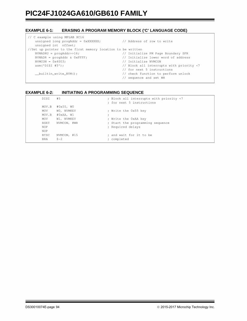
PIC24FJ1024GA610/GB610 FAMILY
EXAMPLE 6-1: ERASING A PROGRAM MEMORY BLOCK (‘C’ LANGUAGE CODE)
EXAMPLE 6-2: INITIATING A PROGRAMMING SEQUENCE
// C example using MPLAB XC16unsigned long progAddr = 0xXXXXXX; // Address of row to writeunsigned int offset;
//Set up pointer to the first memory location to be writtenNVMADRU = progAddr>>16; // Initialize PM Page Boundary SFRNVMADR = progAddr & 0xFFFF; // Initialize lower word of addressNVMCON = 0x4003; // Initialize NVMCONasm("DISI #5"); // Block all interrupts with priority <7
// for next 5 instructions__builtin_write_NVM(); // check function to perform unlock
// sequence and set WR
DISI #5 ; Block all interrupts with priority <7; for next 5 instructions
MOV.B #0x55, W0MOV W0, NVMKEY ; Write the 0x55 key MOV.B #0xAA, W1 ;MOV W1, NVMKEY ; Write the 0xAA keyBSET NVMCON, #WR ; Start the programming sequenceNOP ; Required delaysNOPBTSC NVMCON, #15 ; and wait for it to beBRA $-2 ; completed
DS30010074E-page 94 2015-2017 Microchip Technology Inc.
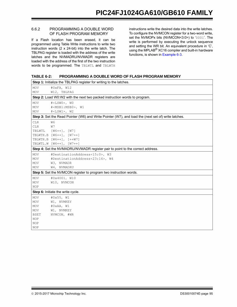
PIC24FJ1024GA610/GB610 FAMILY
6.6.2 PROGRAMMING A DOUBLE WORD OF FLASH PROGRAM MEMORY
If a Flash location has been erased, it can beprogrammed using Table Write instructions to write twoinstruction words (2 x 24-bit) into the write latch. TheTBLPAG register is loaded with the address of the writelatches and the NVMADRU/NVMADR registers areloaded with the address of the first of the two instructionwords to be programmed. The TBLWTL and TBLWTH
instructions write the desired data into the write latches.To configure the NVMCON register for a two-word write,set the NVMOPx bits (NVMCON<3:0>) to ‘0001’. Thewrite is performed by executing the unlock sequenceand setting the WR bit. An equivalent procedure in ‘C’,using the MPLAB® XC16 compiler and built-in hardwarefunctions, is shown in Example 6-3.
TABLE 6-2: PROGRAMMING A DOUBLE WORD OF FLASH PROGRAM MEMORY
Step 1: Initialize the TBLPAG register for writing to the latches.
MOV #0xFA, W12MOV W12, TBLPAG
Step 2: Load W0:W2 with the next two packed instruction words to program.
MOV #<LSW0>, W0MOV #<MSB1:MSB0>, W1MOV #<LSW1>, W2
Step 3: Set the Read Pointer (W6) and Write Pointer (W7), and load the (next set of) write latches.
CLR W6CLR W7TBLWTL [W6++], [W7]TBLWTH.B [W6++], [W7++]TBLWTH.B [W6++], [++W7]TBLWTL.W [W6++], [W7++]
Step 4: Set the NVMADRU/NVMADR register pair to point to the correct address.
MOV #DestinationAddress<15:0>, W3MOV #DestinationAddress<23:16>, W4MOV W3, NVMADRMOV W4, NVMADRU
Step 5: Set the NVMCON register to program two instruction words.
MOV #0x4001, W10MOV W10, NVMCONNOP
Step 6: Initiate the write cycle.
MOV #0x55, W1MOV W1, NVMKEYMOV #0xAA, W1MOV W1, NVMKEYBSET NVMCON, #WRNOPNOPNOP
2015-2017 Microchip Technology Inc. DS30010074E-page 95
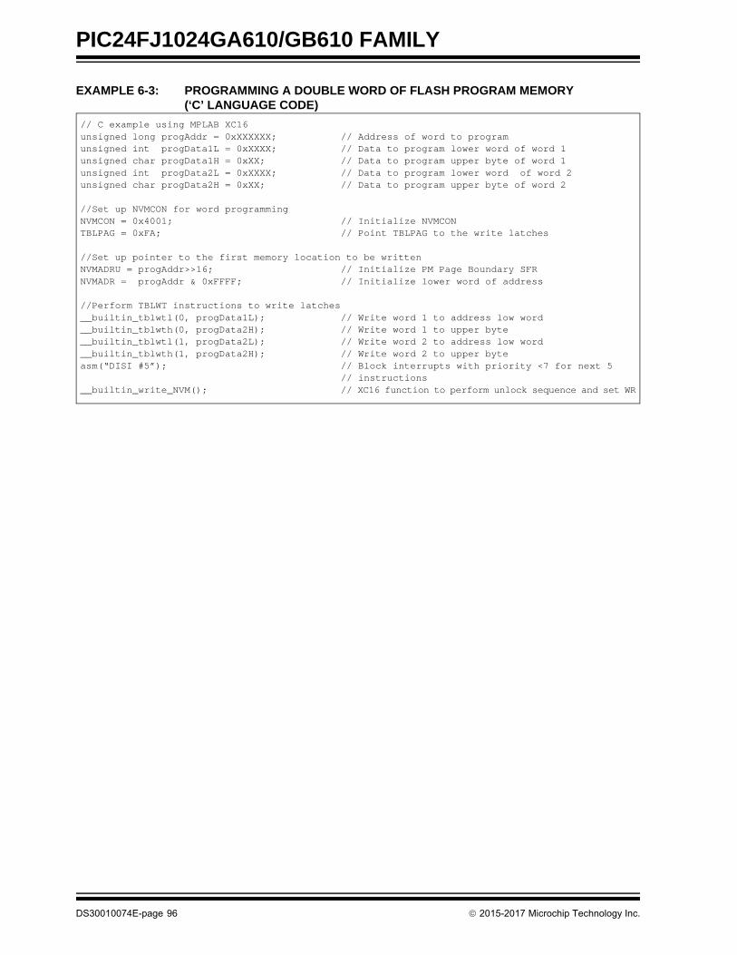
PIC24FJ1024GA610/GB610 FAMILY
EXAMPLE 6-3: PROGRAMMING A DOUBLE WORD OF FLASH PROGRAM MEMORY (‘C’ LANGUAGE CODE)
// C example using MPLAB XC16unsigned long progAddr = 0xXXXXXX; // Address of word to programunsigned int progData1L = 0xXXXX; // Data to program lower word of word 1unsigned char progData1H = 0xXX; // Data to program upper byte of word 1unsigned int progData2L = 0xXXXX; // Data to program lower word of word 2unsigned char progData2H = 0xXX; // Data to program upper byte of word 2
//Set up NVMCON for word programmingNVMCON = 0x4001; // Initialize NVMCONTBLPAG = 0xFA; // Point TBLPAG to the write latches
//Set up pointer to the first memory location to be writtenNVMADRU = progAddr>>16; // Initialize PM Page Boundary SFRNVMADR = progAddr & 0xFFFF; // Initialize lower word of address
//Perform TBLWT instructions to write latches__builtin_tblwtl(0, progData1L); // Write word 1 to address low word__builtin_tblwth(0, progData2H); // Write word 1 to upper byte__builtin_tblwtl(1, progData2L); // Write word 2 to address low word__builtin_tblwth(1, progData2H); // Write word 2 to upper byteasm(“DISI #5”); // Block interrupts with priority <7 for next 5
// instructions__builtin_write_NVM(); // XC16 function to perform unlock sequence and set WR
DS30010074E-page 96 2015-2017 Microchip Technology Inc.

PIC24FJ1024GA610/GB610 FAMILY
7.0 RESETS
The Reset module combines all Reset sources andcontrols the device Master Reset Signal, SYSRST. Thefollowing is a list of device Reset sources:
• POR: Power-on Reset
• MCLR: Master Clear Pin Reset
• SWR: RESET Instruction
• WDT: Watchdog Timer Reset
• BOR: Brown-out Reset
• CM: Configuration Mismatch Reset
• TRAPR: Trap Conflict Reset
• IOPUWR: Illegal Opcode Reset
• UWR: Uninitialized W Register Reset
A simplified block diagram of the Reset module isshown in Figure 7-1.
Any active source of Reset will make the SYSRSTsignal active. Many registers associated with the CPUand peripherals are forced to a known Reset state.Most registers are unaffected by a Reset; their status isunknown on POR and unchanged by all other Resets.
All types of device Reset will set a corresponding statusbit in the RCON register to indicate the type of Reset(see Register 7-1). A POR will clear all bits, except forthe BOR and POR (RCON<1:0>) bits, which are set.The user may set or clear any bit at any time duringcode execution. The RCON bits only serve as statusbits. Setting a particular Reset status bit in software willnot cause a device Reset to occur.
The RCON register also has other bits associated withthe Watchdog Timer and device power-saving states.The function of these bits is discussed in other sectionsof this data sheet.
FIGURE 7-1: RESET SYSTEM BLOCK DIAGRAM
Note: This data sheet summarizes the featuresof this group of PIC24F devices. It is notintended to be a comprehensive refer-ence source. For more information, referto the “dsPIC33/PIC24 Family ReferenceManual”, “Reset” (DS39712), which isavailable from the Microchip web site(www.microchip.com). The informationin this data sheet supersedes theinformation in the FRM.
Note: Refer to the specific peripheral or CPUsection of this manual for register Resetstates.
Note: The status bits in the RCON registershould be cleared after they are read sothat the next RCON register values after adevice Reset will be meaningful.
MCLR
VDD
VDD RiseDetect
POR
Sleep or Idle
Brown-outReset
Enable Voltage Regulator
RESETInstruction
WDTModule
Glitch Filter
BOR
Trap Conflict
Illegal Opcode
Uninitialized W Register
SYSRST
Configuration Mismatch
2015-2017 Microchip Technology Inc. DS30010074E-page 97

PIC24FJ1024GA610/GB610 FAMILY
REGISTER 7-1: RCON: RESET CONTROL REGISTER
R/W-0 R/W-0 R/W-1 R/W-0 U-0 U-0 R/W-0 R/W-0
TRAPR(1) IOPUWR(1) SBOREN RETEN(2) — — CM(1) VREGS(3)
bit 15 bit 8
R/W-0 R/W-0 R/W-0 R/W-0 R/W-0 R/W-0 R/W-1 R/W-1
EXTR(1) SWR(1) SWDTEN(4) WDTO(1) SLEEP(1) IDLE(1) BOR(1) POR(1)
bit 7 bit 0
Legend:
R = Readable bit W = Writable bit U = Unimplemented bit, read as ‘0’
-n = Value at POR ‘1’ = Bit is set ‘0’ = Bit is cleared x = Bit is unknown
bit 15 TRAPR: Trap Reset Flag bit(1)
1 = A Trap Conflict Reset has occurred0 = A Trap Conflict Reset has not occurred
bit 14 IOPUWR: Illegal Opcode or Uninitialized W Access Reset Flag bit(1)
1 = An illegal opcode detection, an illegal address mode or Uninitialized W register is used as anAddress Pointer and caused a Reset
0 = An illegal opcode or Uninitialized W register Reset has not occurred
bit 13 SBOREN: Software Enable/Disable of BOR bit
1 = BOR is turned on in software0 = BOR is turned off in software
bit 12 RETEN: Retention Mode Enable bit(2)
1 = Retention mode is enabled while device is in Sleep modes (1.2V regulator enabled)0 = Retention mode is disabled
bit 11-10 Unimplemented: Read as ‘0’
bit 9 CM: Configuration Word Mismatch Reset Flag bit(1)
1 = A Configuration Word Mismatch Reset has occurred0 = A Configuration Word Mismatch Reset has not occurred
bit 8 VREGS: Fast Wake-up from Sleep bit(3)
1 = Fast wake-up is enabled (uses more power) 0 = Fast wake-up is disabled (uses less power)
bit 7 EXTR: External Reset (MCLR) Pin bit(1)
1 = A Master Clear (pin) Reset has occurred0 = A Master Clear (pin) Reset has not occurred
bit 6 SWR: Software Reset (Instruction) Flag bit(1)
1 = A RESET instruction has been executed0 = A RESET instruction has not been executed
Note 1: All of the Reset status bits may be set or cleared in software. Setting one of these bits in software does not cause a device Reset.
2: If the LPCFG Configuration bit is ‘1’ (unprogrammed), the retention regulator is disabled and the RETEN bit has no effect. Retention mode preserves the SRAM contents during Sleep.
3: Re-enabling the regulator after it enters Standby mode will add a delay, TVREG, when waking up from Sleep. Applications that do not use the voltage regulator should set this bit to prevent this delay from occurring.
4: If the FWDTEN<1:0> Configuration bits are ‘11’ (unprogrammed), the WDT is always enabled, regardless of the SWDTEN bit setting.
DS30010074E-page 98 2015-2017 Microchip Technology Inc.
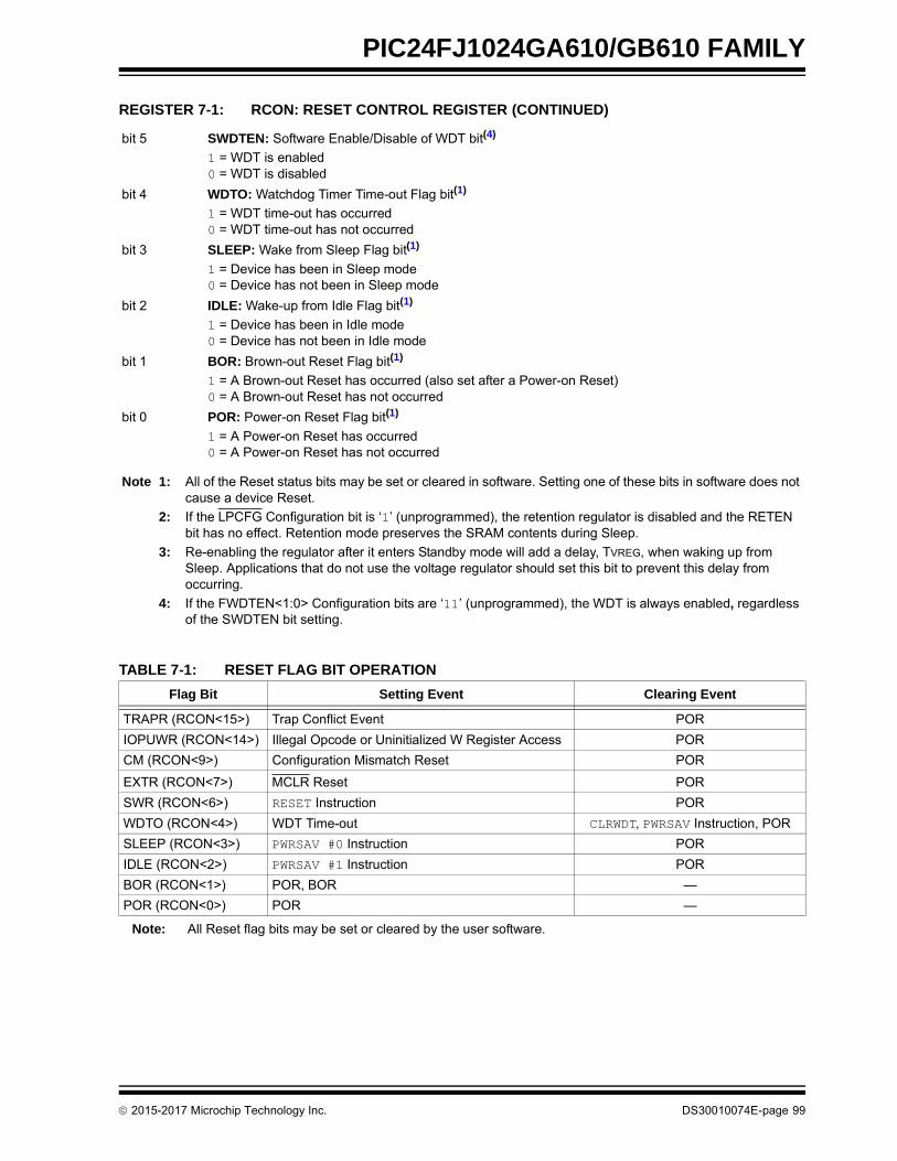
PIC24FJ1024GA610/GB610 FAMILY
TABLE 7-1: RESET FLAG BIT OPERATION
bit 5 SWDTEN: Software Enable/Disable of WDT bit(4)
1 = WDT is enabled0 = WDT is disabled
bit 4 WDTO: Watchdog Timer Time-out Flag bit(1)
1 = WDT time-out has occurred0 = WDT time-out has not occurred
bit 3 SLEEP: Wake from Sleep Flag bit(1)
1 = Device has been in Sleep mode0 = Device has not been in Sleep mode
bit 2 IDLE: Wake-up from Idle Flag bit(1)
1 = Device has been in Idle mode0 = Device has not been in Idle mode
bit 1 BOR: Brown-out Reset Flag bit(1)
1 = A Brown-out Reset has occurred (also set after a Power-on Reset)0 = A Brown-out Reset has not occurred
bit 0 POR: Power-on Reset Flag bit(1)
1 = A Power-on Reset has occurred0 = A Power-on Reset has not occurred
Flag Bit Setting Event Clearing Event
TRAPR (RCON<15>) Trap Conflict Event POR
IOPUWR (RCON<14>) Illegal Opcode or Uninitialized W Register Access POR
CM (RCON<9>) Configuration Mismatch Reset POR
EXTR (RCON<7>) MCLR Reset POR
SWR (RCON<6>) RESET Instruction POR
WDTO (RCON<4>) WDT Time-out CLRWDT, PWRSAV Instruction, POR
SLEEP (RCON<3>) PWRSAV #0 Instruction POR
IDLE (RCON<2>) PWRSAV #1 Instruction POR
BOR (RCON<1>) POR, BOR —
POR (RCON<0>) POR —
Note: All Reset flag bits may be set or cleared by the user software.
REGISTER 7-1: RCON: RESET CONTROL REGISTER (CONTINUED)
Note 1: All of the Reset status bits may be set or cleared in software. Setting one of these bits in software does not cause a device Reset.
2: If the LPCFG Configuration bit is ‘1’ (unprogrammed), the retention regulator is disabled and the RETEN bit has no effect. Retention mode preserves the SRAM contents during Sleep.
3: Re-enabling the regulator after it enters Standby mode will add a delay, TVREG, when waking up from Sleep. Applications that do not use the voltage regulator should set this bit to prevent this delay from occurring.
4: If the FWDTEN<1:0> Configuration bits are ‘11’ (unprogrammed), the WDT is always enabled, regardless of the SWDTEN bit setting.
2015-2017 Microchip Technology Inc. DS30010074E-page 99

PIC24FJ1024GA610/GB610 FAMILY
7.1 Special Function Register Reset States
Most of the Special Function Registers (SFRs) associ-ated with the PIC24F CPU and peripherals are reset to aparticular value at a device Reset. The SFRs aregrouped by their peripheral or CPU function and theirReset values are specified in each section of this manual.
The Reset value for each SFR does not depend on thetype of Reset, with the exception of four registers. TheReset value for the Reset Control register, RCON, willdepend on the type of device Reset. The Reset valuefor the Oscillator Control register, OSCCON, willdepend on the type of Reset and the programmedvalues of the FNOSC<2:0> bits in the FOSCSEL FlashConfiguration Word (see Table 7-2). The NVMCONregister is only affected by a POR.
7.2 Device Reset Times
The Reset times for various types of device Reset aresummarized in Table 7-3. Note that the Master ResetSignal, SYSRST, is released after the POR delay timeexpires.
The time at which the device actually begins to executecode will also depend on the system oscillator delays,which include the Oscillator Start-up Timer (OST) andthe PLL lock time. The OST and PLL lock times occurin parallel with the applicable SYSRST delay times.
The Fail-Safe Clock Monitor (FSCM) delay determinesthe time at which the FSCM begins to monitor the systemclock source after the SYSRST signal is released.
7.3 Brown-out Reset (BOR)
PIC24FJ1024GA610/GB610 family devices implement aBOR circuit that provides the user with several configura-tion and power-saving options. The BOR is controlled bythe BOREN<1:0> (FPOR<1:0>) Configuration bits.
When BOR is enabled, any drop of VDD below the BORthreshold results in a device BOR. Threshold levels aredescribed in Section 33.1 “DC Characteristics”.
7.4 Clock Source Selection at Reset
If clock switching is enabled, the system clock source atdevice Reset is chosen, as shown in Table 7-2. If clockswitching is disabled, the system clock source is alwaysselected according to the Oscillator Configuration bits.For more information, refer to the “dsPIC33/PIC24Family Reference Manual”, “Oscillator” (DS39700).
TABLE 7-2: OSCILLATOR SELECTION vs. TYPE OF RESET (CLOCK SWITCHING ENABLED)
Reset Type Clock Source Determinant
POR FNOSC<2:0> Configuration bits(FOSCSEL<2:0>)BOR
MCLRCOSC<2:0> Control bits (OSCCON<14:12>)
WDTO
SWR
DS30010074E-page 100 2015-2017 Microchip Technology Inc.

PIC24FJ1024GA610/GB610 FAMILY
TABLE 7-3: RESET DELAY TIMES FOR VARIOUS DEVICE RESETS
Reset Type Clock Source SYSRST DelaySystem Clock
Delay Notes
POR EC TPOR + TSTARTUP + TRST — 1, 2, 3
ECPLL TPOR + TSTARTUP + TRST TLOCK 1, 2, 3, 5
XT, HS, SOSC TPOR + TSTARTUP + TRST TOST 1, 2, 3, 4
XTPLL, HSPLL TPOR + TSTARTUP + TRST TOST + TLOCK 1, 2, 3, 4, 5
FRC, OSCFDIV TPOR + TSTARTUP + TRST TFRC 1, 2, 3, 6, 7
FRCPLL TPOR + TSTARTUP + TRST TFRC + TLOCK 1, 2, 3, 5, 6
LPRC TPOR + TSTARTUP + TRST TLPRC 1, 2, 3, 6
DCO TPOR + TSTARTUP + TRST TDCO 1, 2, 3, 8
BOR EC TSTARTUP + TRST — 2, 3
ECPLL TSTARTUP + TRST TLOCK 2, 3, 5
XT, HS, SOSC TSTARTUP + TRST TOST 2, 3, 4
XTPLL, HSPLL TSTARTUP + TRST TOST + TLOCK 2, 3, 4, 5
FRC, OSCFDIV TSTARTUP + TRST TFRC 2, 3, 6, 7
FRCPLL TSTARTUP + TRST TFRC + TLOCK 2, 3, 5, 6
LPRC TSTARTUP + TRST TLPRC 2, 3, 6
DCO TPOR + TSTARTUP + TRST TDCO 1, 2, 3, 8
MCLR Any Clock TRST — 3
WDT Any Clock TRST — 3
Software Any clock TRST — 3
Illegal Opcode Any Clock TRST — 3
Uninitialized W Any Clock TRST — 3
Trap Conflict Any Clock TRST — 3
Note 1: TPOR = Power-on Reset Delay (10 s nominal).
2: TSTARTUP = TVREG.
3: TRST = Internal State Reset Time (2 s nominal).
4: TOST = Oscillator Start-up Timer (OST). A 10-bit counter counts 1024 oscillator periods before releasing the oscillator clock to the system.
5: TLOCK = PLL Lock Time.
6: TFRC and TLPRC = RC Oscillator Start-up Times.
7: If Two-Speed Start-up is enabled, regardless of the Primary Oscillator selected, the device starts with FRC so the system clock delay is just TFRC, and in such cases, FRC start-up time is valid; it switches to the Primary Oscillator after its respective clock delay.
8: TDCO = DCO Start-up and Stabilization Times.
2015-2017 Microchip Technology Inc. DS30010074E-page 101

PIC24FJ1024GA610/GB610 FAMILY
7.4.1 POR AND LONG OSCILLATOR START-UP TIMES
The oscillator start-up circuitry and its associated delaytimers are not linked to the device Reset delays thatoccur at power-up. Some crystal circuits (especially low-frequency crystals) will have a relatively long start-uptime. Therefore, one or more of the following conditionsis possible after SYSRST is released:
• The oscillator circuit has not begun to oscillate.
• The Oscillator Start-up Timer has not expired (if a crystal oscillator is used).
• The PLL has not achieved a lock (if PLL is used).
The device will not begin to execute code until a validclock source has been released to the system. There-fore, the oscillator and PLL start-up delays must beconsidered when the Reset delay time must be known.
7.4.2 FAIL-SAFE CLOCK MONITOR (FSCM) AND DEVICE RESETS
If the FSCM is enabled, it will begin to monitor thesystem clock source when SYSRST is released. If avalid clock source is not available at this time, thedevice will automatically switch to the FRC Oscillatorand the user can switch to the desired crystal oscillatorin the Trap Service Routine (TSR).
DS30010074E-page 102 2015-2017 Microchip Technology Inc.

PIC24FJ1024GA610/GB610 FAMILY
8.0 INTERRUPT CONTROLLER
The PIC24FJ1024GA610/GB610 family interruptcontroller reduces the numerous peripheral interruptrequest signals to a single interrupt request signal tothe PIC24FJ1024GA610/GB610 family CPU.
The interrupt controller has the following features:
• Up to Eight Processor Exceptions and Software Traps
• Seven User-Selectable Priority Levels
• Interrupt Vector Table (IVT) with a Unique Vector for Each Interrupt or Exception Source
• Fixed Priority within a Specified User Priority Level
• Fixed Interrupt Entry and Return Latencies
8.1 Interrupt Vector Table
The PIC24FJ1024GA610/GB610 family InterruptVector Table (IVT), shown in Figure 8-1, resides inprogram memory starting at location, 000004h. TheIVT contains 6 non-maskable trap vectors and up to118 sources of interrupt. In general, each interruptsource has its own vector. Each interrupt vectorcontains a 24-bit wide address. The value programmedinto each interrupt vector location is the startingaddress of the associated Interrupt Service Routine(ISR).
Interrupt vectors are prioritized in terms of their naturalpriority. This priority is linked to their position in thevector table. Lower addresses generally have a highernatural priority. For example, the interrupt associatedwith Vector 0 takes priority over interrupts at any othervector address.
8.1.1 ALTERNATE INTERRUPT VECTOR TABLE
The Alternate Interrupt Vector Table (AIVT) is locatedafter the IVT, as shown in Figure 8-1. The AIVTEN(INTCON2<8>) control bit provides access to the AIVT.If the AIVTEN bit is set, all interrupt and exceptionprocesses will use the alternate vectors instead of thedefault vectors. The alternate vectors are organized inthe same manner as the default vectors.
The AIVT is available only if the Boot Segment hasbeen defined and the AIVT has been enabled. Toenable the AIVT, both the Configuration bit, AIVTDIS(FSEC<15>), and the AIVTEN bit (INTCON2<8> in theSFR), have to be set. When the AIVT is enabled, allinterrupts and exception processes use the alternatevectors instead of the default vectors. The AIVT beginsat the start of the last page of the Boot Segment (BS)defined by the BSLIM<12:0> bits. The AIVT address is:(BSLIM<12:0> – 1) x 0x800.
8.2 Reset Sequence
A device Reset is not a true exception because theinterrupt controller is not involved in the Reset process.The PIC24FJ1024GA610/GB610 family devices cleartheir registers in response to a Reset, which forces thePC to zero. The device then begins program executionat location, 0x000000. A GOTO instruction at the Resetaddress can redirect program execution to theappropriate start-up routine.
Note 1: This data sheet summarizes the features ofthe PIC24FJ1024GA610/GB610 family ofdevices. It is not intended to be a compre-hensive reference source. To complementthe information in this data sheet, referto “Interrupts” (DS70000600) in the“dsPIC33/PIC24 Family Reference Man-ual”, which is available from the Microchipweb site (www.microchip.com). The infor-mation in this data sheet supersedes theinformation in the FRM.
2: Some registers and associated bitsdescribed in this section may not beavailable on all devices. Refer toSection 4.0 “Memory Organization” inthis data sheet for device-specific registerand bit information.
Note: Any unimplemented or unused vectorlocations in the IVT should beprogrammed with the address of a defaultinterrupt handler routine that contains aRESET instruction.
2015-2017 Microchip Technology Inc. DS30010074E-page 103

PIC24FJ1024GA610/GB610 FAMILY
FIGURE 8-1: PIC24FJ1024GA610/GB610 FAMILY INTERRUPT VECTOR TABLES
TABLE 8-1: TRAP VECTOR DETAILS
Vector Number IVT Address AIVT Address Trap Source
0 000004h BOA+04h Oscillator Failure
1 000006h BOA+06h Address Error
2 000008h BOA+08h General Hardware Error
3 00000Ah BOA+0Ah Stack Error
4 00000Ch BOA+0Ch Math Error
5 00000Eh BOA+0Eh Reserved
6 000010h BOA+10h General Software Error
7 000012h BOA+12h Reserved
Legend: BOA = Base Offset Address for the AIVT segment, which is the starting address of the last page of the Boot Segment.
The BOA depends on the size of the Boot Segment defined by BSLIM<12:0>:[(BSLIM<12:0> – 1) x 0x800]
Legend: BOA: Base Offset Address for AIVT, which is the starting address of the last page of the Boot Segment. All addresses are in hexadecimal.
Note 1: See Table 8-2 for the interrupt vector list. 2: AIVT is only available when a Boot Segment is implemented.
Reset – GOTO Instruction 000000hReset – GOTO Address 000002h
Oscillator Fail Trap Vector 000004hAddress Error Trap VectorGeneral Hard Trap VectorStack Error Trap VectorMath Error Trap Vector
ReservedGeneral Soft Trap Vector
ReservedInterrupt Vector 0 000014hInterrupt Vector 1
——
Interrupt Vector 52 00007ChInterrupt Vector 53 00007EhInterrupt Vector 54 000080h
——
Interrupt Vector 116 0000FChInterrupt Vector 117 0000FEh
De
cre
asi
ng
Na
tura
l Ord
er
Pri
ori
ty
Interrupt Vector Table (IVT)(1) Alternate Interrupt Vector Table (AIVT)(1,2)
Reserved BOA+00hReserved BOA+02h
Oscillator Fail Trap Vector BOA+04hAddress Error Trap VectorGeneral Hard Trap VectorStack Error Trap VectorMath Error Trap Vector
ReservedGeneral Soft Trap Vector
ReservedInterrupt Vector 0 BOA+14hInterrupt Vector 1
——
Interrupt Vector 52 BOA+7ChInterrupt Vector 53 BOA+7EhInterrupt Vector 54 BOA+80h
——
Interrupt Vector 116Interrupt Vector 117 BOA+FEh
(Start of Code) (BOA+100h)
DS30010074E-page 104 2015-2017 Microchip Technology Inc.

PIC24FJ1024GA610/GB610 FAMILY
TABLE 8-2: INTERRUPT VECTOR DETAILS
Interrupt SourceIRQ
#IVT Address
Interrupt Bit Location
Flag Enable Priority
Highest Natural Order Priority
INT0 – External Interrupt 0 0 000014h IFS0<0> IEC0<0> INT0Interrupt
IC1 – Input Capture 1 1 000016h IFS0<1> IEC0<1> IC1Interrupt
OC1 – Output Compare 1 2 000018h IFS0<2> IEC0<2> OC1Interrupt
T1 – Timer1 3 00001Ah IFS0<3> IEC0<3> T1Interrupt
DMA0 – Direct Memory Access 0 4 00001Ch IFS0<4> IEC0<4> DMA0Interrupt
IC2 – Input Capture 2 5 00001Eh IFS0<5> IEC0<5> IC2Interrupt
OC2 – Output Compare 2 6 000020h IFS0<6> IEC0<6> OC2Interrupt
T2 – Timer2 7 000022h IFS0<7> IEC0<7> T2Interrupt
T3 – Timer3 8 000024h IFS0<8> IEC0<8> T3Interrupt
SPI1 – SPI1 General 9 000026h IFS0<9> IEC0<9> SPI1Interrupt
SPI1TX – SPI1 Transfer Done 10 000028h IFS0<10> IEC0<10> SPI1TXInterrupt
U1RX – UART1 Receiver 11 00002Ah IFS0<11> IEC0<11> U1RXInterrupt
U1TX – UART1 Transmitter 12 00002Ch IFS0<12> IEC0<12> U1TXInterrupt
ADC1 – A/D Converter 1 13 00002Eh IFS0<13> IEC0<13> ADC1Interrupt
DMA1 – Direct Memory Access 1 14 000030h IFS0<14> IEC0<14> DMA1Interrupt
NVM – NVM Program/Erase Complete 15 000032h IFS0<15> IEC0<15> NVMInterrupt
SI2C1 – I2C1 Slave Events 16 000034h IFS1<0> IEC1<0> SI2C1Interrupt
MI2C1 – I2C1 Master Events 17 000036h IFS1<1> IEC1<1> MI2C1Interrupt
Comp – Comparator 18 000038h IFS1<2> IEC1<2> CompInterrupt
IOC – Interrupt-on-Change Interrupt 19 00003Ah IFS1<3> IEC1<3> IOCInterrupt
INT1 – External Interrupt 1 20 00003Ch IFS1<4> IEC1<4> INT1Interrupt
— 21 — — — —
CCP5 – Capture/Compare 5 22 000040h IFS1<6> IEC1<6> CCP5Interrupt
CCP6 – Capture/Compare 6 23 000042h IFS1<7> IEC1<7> CCP6Interrupt
DMA2 – Direct Memory Access 2 24 000044h IFS1<8> IEC1<8> DMA2Interrupt
OC3 – Output Compare 3 25 000046h IFS1<9> IEC1<9> OC3Interrupt
OC4 – Output Compare 4 26 000048h IFS1<10> IEC1<10> OC4Interrupt
T4 – Timer4 27 00004Ah IFS1<11> IEC1<11> T4Interrupt
T5 – Timer5 28 00004Ch IFS1<12> IEC1<12> T5Interrupt
INT2 – External Interrupt 2 29 00004Eh IFS1<13> IEC1<13> INT2Interrupt
U2RX – UART2 Receiver 30 000050h IFS1<14> IEC1<14> U2RXInterrupt
U2TX – UART2 Transmitter 31 000052h IFS1<15> IEC1<15> U2TXInterrupt
SPI2 – SPI2 General 32 000054h IFS2<0> IEC2<0> SPI2Interrupt
SPI2TX – SPI2 Transfer Done 33 000056h IFS2<1> IEC2<1> SPI2TXInterrupt
— 34 — — — —
— 35 — — — —
DMA3 – Direct Memory Access 3 36 00005Ch IFS2<4> IEC2<4> DMA3Interrupt
IC3 – Input Capture 3 37 00005Eh IFS2<5> IEC2<5> IC3Interrupt
IC4 – Input Capture 4 38 000060h IFS2<6> IEC2<6> IC4Interrupt
IC5 – Input Capture 5 39 000062h IFS2<7> IEC2<7> IC5Interrupt
IC6 – Input Capture 6 40 000064h IFS2<8> IEC2<8> IC6Interrupt
2015-2017 Microchip Technology Inc. DS30010074E-page 105

PIC24FJ1024GA610/GB610 FAMILY
OC5 – Output Compare 5 41 000066h IFS2<9> IEC2<9> OC5Interrupt
OC6 – Output Compare 6 42 000068h IFS2<10> IEC2<10> OC6Interrupt
CCT3 – Capture/Compare Timer3 43 00006Ah IFS2<11> IEC2<11> CCT3Interrupt
CCT4 – Capture/Compare Timer4 44 00006Ch IFS2<12> IEC2<12> CCT4Interrupt
PMP – Parallel Master Port 45 00006Eh IFS2<13> IEC2<13> PMPInterrupt
DMA4 – Direct Memory Access 4 46 000070h IFS2<14> IEC2<14> DMA4Interrupt
CCT5 – Capture/Compare Timer5 47 000072h IFS2<15> IEC2<15> CCT5Interrupt
CCT6 – Capture/Compare Timer6 48 000074h IFS3<0> IEC3<0> CCT6Interrupt
SI2C2 – I2C2 Slave Events 49 000076h IFS3<1> IEC3<1> SI2C2Interrupt
MI2C2 – I2C2 Master Events 50 000078h IFS3<2> IEC3<2> MI2C2Interrupt
CCT7 – Capture/Compare Timer7 51 00007Ah IFS3<3> IEC3<3> CCT7Interrupt
— 52 — — — —
INT3 – External Interrupt 3 53 00007Eh IFS3<5> IEC3<5> INT3Interrupt
INT4 – External Interrupt 4 54 000080h IFS3<6> IEC3<6> INT4Interrupt
— 55 — — — —
— 56 — — — —
— 57 — — — —
SPI1RX – SPI1 Receive Done 58 000088h IFS3<10> IEC3<10> SPI1RXInterrupt
SPI2RX – SPI2 Receive Done 59 00008Ah IFS3<11> IEC3<11> SPI2RXInterrupt
SPI3RX – SPI3 Receive Done 60 00008Ch IFS3<12> IEC3<12> SPI3RXInterrupt
DMA5 – Direct Memory Access 5 61 00008Eh IFS3<13> IEC3<13> DMA5Interrupt
RTCC – Real-Time Clock and Calendar 62 000090h IFS3<14> IEC3<14> RTCCInterrupt
CCP1 – Capture/Compare 1 63 000092h IFS3<15> IEC3<15> CCP1Interrupt
CCP2 – Capture/Compare 2 64 000094h IFS4<0> IEC4<0> CCP2Interrupt
U1E – UART1 Error 65 000096h IFS4<1> IEC4<1> U1ErrInterrupt
U2E – UART2 Error 66 000098h IFS4<2> IEC4<2> U2ErrInterrupt
CRC – Cyclic Redundancy Check 67 00009Ah IFS4<3> IEC4<3> CRCInterrupt
DMA6 – Direct Memory Access 6 68 00009Ch IFS4<4> IEC4<4> DMA6Interrupt
DMA7 – Direct Memory Access 7 69 00009Eh IFS4<5> IEC4<5> DMA7Interrupt
SI2C3 – I2C3 Slave Events 70 0000A0h IFS4<6> IEC4<6> SI2C3Interrupt
MI2C3 – I2C3 Master Events 71 0000A2h IFS4<7> IEC4<7> MI2C3Interrupt
HLVD – High/Low-Voltage Detect 72 0000A4h IFS4<8> IEC4<8> HLVDInterrupt
CCP7 – Capture/Compare 7 73 0000A6h IFS4<9> IEC4<9> CCP7Interrupt
— 74 74 — — —
— 75 75 — — —
— 76 76 — — —
CTMU – Interrupt 77 0000AEh IFS4<13> IEC4<13> CTMUInterrupt
— 78 78 — — —
— 79 79 — — —
— 80 80 — — —
U3E – UART3 Error 81 0000B6h IFS5<1> IEC5<1> U3ErrInterrupt
U3RX – UART3 Receiver 82 0000B8h IFS5<2> IEC5<2> U3RXInterrupt
U3TX – UART3 Transmitter 83 0000BAh IFS5<3> IEC5<3> U3TXInterrupt
TABLE 8-2: INTERRUPT VECTOR DETAILS (CONTINUED)
Interrupt SourceIRQ
#IVT Address
Interrupt Bit Location
Flag Enable Priority
DS30010074E-page 106 2015-2017 Microchip Technology Inc.

PIC24FJ1024GA610/GB610 FAMILY
I2C1BC – I2C1 Bus Collision 84 0000BCh IFS5<4> IEC5<4> I2C1BCInterrupt
I2C2BC – I2C2 Bus Collision 85 0000BEh IFS5<5> IEC5<5> I2C2BCInterrupt
USB1 – USB1 Interrupt 86 0000C0h IFS5<6> IEC5<6> USB1Interrupt
U4E – UART4 Error 87 0000C2h IFS5<7> IEC5<7> U4ErrInterrupt
U4RX – UART4 Receiver 88 0000C4h IFS5<8> IEC5<8> U4RXInterrupt
U4TX – UART4 Transmitter 89 0000C6h IFS5<9> IEC5<9> U4TXInterrupt
SPI3 – SPI3 General 90 0000C8h IFS5<10> IEC5<10> SPI3Interrupt
SPI3TX – SPI3 Transfer Done 91 0000CAh IFS5<11> IEC5<11> SPI3TXInterrupt
— 92 92 — — —
— 93 93 — — —
CCP3 – Capture/Compare 3 94 0000D0h IFS5<14> IEC5<14> CCP3Interrupt
CCP4 – Capture/Compare 4 95 0000D2h IFS5<15> IEC5<15> CCP4Interrupt
CLC1 – Configurable Logic Cell 1 96 0000D4h IFS6<0> IEC6<0> CLC1Interrupt
CLC2 – Configurable Logic Cell 2 97 0000D6h IFS6<1> IEC6<1> CLC2Interrupt
CLC3 – Configurable Logic Cell 3 98 0000D8h IFS6<2> IEC6<2> CLC3Interrupt
CLC4 – Configurable Logic Cell 4 99 0000DAh IFS6<3> IEC6<3> CLC4Interrupt
— 100 — — — —
CCT1 – Capture/Compare Timer1 101 0000DEh IFS6<5> IEC6<5> CCT1Interrupt
CCT2 – Capture/Compare Timer2 102 0000E0h IFS6<6> IEC6<6> CCT2Interrupt
— 103 — — — —
— 104 — — — —
— 105 — — — —
FST – FRC Self-Tuning Interrupt 106 0000E8h IFS6<10> IEC6<10> FSTInterrupt
— 107 — — — —
— 108 — — — —
I2C3BC – I2C3 Bus Collision 109 0000EEh IFS6<13> IEC6<13> I2C3BCInterrupt
RTCCTS – Real-Time Clock Timestamp 110 0000F0h IFS6<14> IEC6<14> RTCCTSInterrupt
U5RX – UART5 Receiver 111 0000F2h IFS6<15> IEC6<15> U5RXInterrupt
U5TX – UART5 Transmitter 112 0000F4h IFS7<0> IEC7<0> U5TXInterrupt
U5E – UART5 Error 113 0000F6h IFS7<1> IEC7<1> U5ErrInterrupt
U6RX – UART6 Receiver 114 0000F8h IFS7<2> IEC7<2> U6RXInterrupt
U6TX – UART6 Transmitter 115 0000FAh IFS7<3> IEC7<3> U6TXInterrupt
U6E – UART6 Error 116 0000FCh IFS7<4> IEC7<4> U6ErrInterrupt
JTAG – JTAG 117 0000FEh IFS7<5> IEC7<5> JTAGInterrupt
TABLE 8-2: INTERRUPT VECTOR DETAILS (CONTINUED)
Interrupt SourceIRQ
#IVT Address
Interrupt Bit Location
Flag Enable Priority
2015-2017 Microchip Technology Inc. DS30010074E-page 107

PIC24FJ1024GA610/GB610 FAMILY
8.3 Interrupt Resources
Many useful resources are provided on the main prod-uct page of the Microchip web site for the devices listedin this data sheet. This product page, which can beaccessed using this link, contains the latest updatesand additional information.
8.3.1 KEY RESOURCES
• “Interrupts” (DS70000600) in the “dsPIC33/PIC24 Family Reference Manual”
• Code Samples
• Application Notes
• Software Libraries
• Webinars
• All Related “dsPIC33/PIC24 Family Reference Manual” Sections
• Development Tools
8.4 Interrupt Control and Status Registers
PIC24FJ1024GA610/GB610 family devices implementthe following registers for the interrupt controller:
• INTCON1
• INTCON2
• INTCON4
• IFS0 through IFS7
• IEC0 through IEC7
• IPC0 through IPC29
• INTTREG
8.4.1 INTCON1-INTCON4
Global interrupt control functions are controlled fromINTCON1 and INTCON2. INTCON1 contains theInterrupt Nesting Disable (NSTDIS) bit, as well as thecontrol and status flags for the processor trap sources.
The INTCON2 register controls global interruptgeneration, the external interrupt request signalbehavior and the use of the Alternate Interrupt VectorTable (AIVT).
The INTCON4 register contains the SoftwareGenerated Hard Trap bit (SGHT) and ECC Double-BitError (ECCDBE) trap.
8.4.2 IFSx
The IFSx registers maintain all of the interrupt requestflags. Each source of interrupt has a status bit, which isset by the respective peripherals or external signal, andis cleared via software.
8.4.3 IECx
The IECx registers maintain all of the interrupt enablebits. These control bits are used to individually enableinterrupts from the peripherals or external signals.
8.4.4 IPCx
The IPCx registers are used to set the Interrupt PriorityLevel (IPL) for each source of interrupt. Each userinterrupt source can be assigned to one of eight prioritylevels.
8.4.5 INTTREG
The INTTREG register contains the associatedinterrupt vector number and the new CPU InterruptPriority Level, which are latched into the VectorNumber bits (VECNUM<7:0>) and Interrupt PriorityLevel bits (ILR<3:0>) fields in the INTTREG register.The new Interrupt Priority Level is the priority of thepending interrupt.
The interrupt sources are assigned to the IFSx, IECxand IPCx registers in the same sequence as they arelisted in Table 8-2. For example, the INT0 (ExternalInterrupt 0) is shown as having Vector Number 8 and anatural order priority of 0. Thus, the INT0IF bit is foundin IFS0<0>, the INT0IE bit in IEC0<0> and the INT0IPbits in the first position of IPC0 (IPC0<2:0>).
8.4.6 STATUS/CONTROL REGISTERS
Although these registers are not specifically part of theinterrupt control hardware, two of the CPU Controlregisters contain bits that control interrupt functionality.For more information on these registers refer to “CPUwith Extended Data Space (EDS)” (DS39732) in the“dsPIC33/PIC24 Family Reference Manual”.
• The CPU STATUS Register, SR, contains the IPL<2:0> bits (SR<7:5>). These bits indicate the current CPU Interrupt Priority Level. The user software can change the current CPU Interrupt Priority Level by writing to the IPLx bits.
• The CORCON register contains the IPL3 bit, which together with the IPL<2:0> bits, also indi-cates the current CPU Interrupt Priority Level. IPL3 is a read-only bit so that trap events cannot be masked by the user software.
All Interrupt registers are described in Register 8-3through Register 8-6 in the following pages.
Note: In the event you are not able to access theproduct page using the link above, enterthis URL in your browser:http://www.microchip.com/wwwproducts/Devices.aspx?dDocName=en555464
DS30010074E-page 108 2015-2017 Microchip Technology Inc.
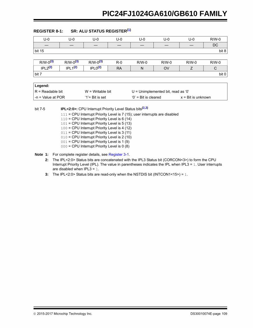
PIC24FJ1024GA610/GB610 FAMILY
REGISTER 8-1: SR: ALU STATUS REGISTER(1)
U-0 U-0 U-0 U-0 U-0 U-0 U-0 R/W-0
— — — — — — — DC
bit 15 bit 8
R/W-0(3) R/W-0(3) R/W-0(3) R-0 R/W-0 R/W-0 R/W-0 R/W-0
IPL2(2) IPL1(2) IPL0(2) RA N OV Z C
bit 7 bit 0
Legend:
R = Readable bit W = Writable bit U = Unimplemented bit, read as ‘0’
-n = Value at POR ‘1’= Bit is set ‘0’ = Bit is cleared x = Bit is unknown
bit 7-5 IPL<2:0>: CPU Interrupt Priority Level Status bits(2,3)
111 = CPU Interrupt Priority Level is 7 (15); user interrupts are disabled 110 = CPU Interrupt Priority Level is 6 (14)101 = CPU Interrupt Priority Level is 5 (13)100 = CPU Interrupt Priority Level is 4 (12)011 = CPU Interrupt Priority Level is 3 (11)010 = CPU Interrupt Priority Level is 2 (10)001 = CPU Interrupt Priority Level is 1 (9)000 = CPU Interrupt Priority Level is 0 (8)
Note 1: For complete register details, see Register 3-1.
2: The IPL<2:0> Status bits are concatenated with the IPL3 Status bit (CORCON<3>) to form the CPU Interrupt Priority Level (IPL). The value in parentheses indicates the IPL when IPL3 = 1. User interrupts are disabled when IPL3 = 1.
3: The IPL<2:0> Status bits are read-only when the NSTDIS bit (INTCON1<15>) = 1.
2015-2017 Microchip Technology Inc. DS30010074E-page 109

PIC24FJ1024GA610/GB610 FAMILY
REGISTER 8-2: CORCON: CPU CORE CONTROL REGISTER(1)
U-0 U-0 U-0 U-0 U-0 U-0 U-0 U-0
— — — — — — — —
bit 15 bit 8
U-0 U-0 U-0 U-0 R/C-0 R/W-1 U-0 U-0
— — — — IPL3(2) PSV — —
bit 7 bit 0
Legend: C = Clearable bit
R = Readable bit W = Writable bit U = Unimplemented bit, read as ‘0’
-n = Value at POR ‘1’= Bit is set ‘0’ = Bit is cleared x = Bit is unknown
bit 15-4 Unimplemented: Read as ‘0’
bit 3 IPL3: CPU Interrupt Priority Level Status bit(2)
1 = CPU Interrupt Priority Level is greater than 70 = CPU Interrupt Priority Level is 7 or less
bit 2 PSV: Not used as part of the interrupt module
bit 1-0 Unimplemented: Read as ‘0’
Note 1: For complete register details, see Register 3-2.
2: The IPL<2:0> Status bits are concatenated with the IPL3 Status bit (CORCON<3>) to form the CPU Interrupt Priority Level (IPL). The value in parentheses indicates the IPL when IPL3 = 1. User interrupts are disabled when IPL3 = 1.
DS30010074E-page 110 2015-2017 Microchip Technology Inc.
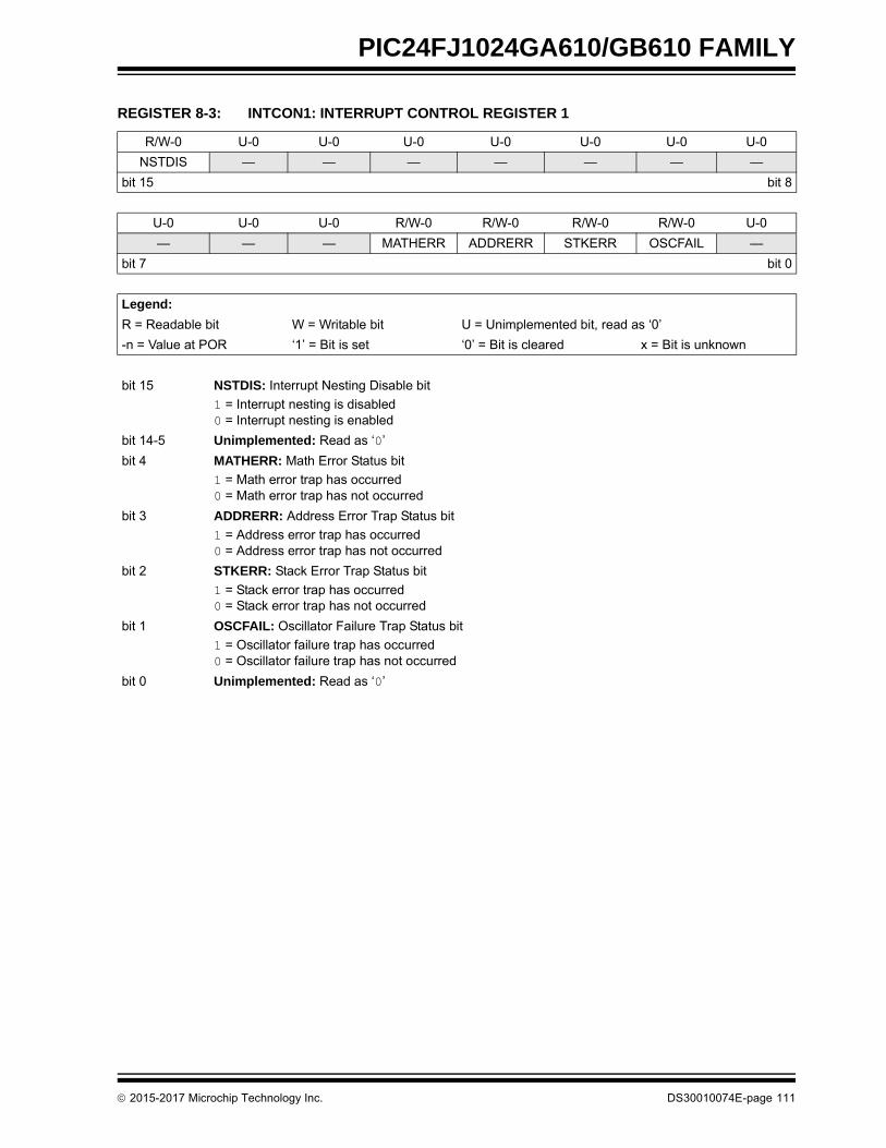
PIC24FJ1024GA610/GB610 FAMILY
REGISTER 8-3: INTCON1: INTERRUPT CONTROL REGISTER 1
R/W-0 U-0 U-0 U-0 U-0 U-0 U-0 U-0
NSTDIS — — — — — — —
bit 15 bit 8
U-0 U-0 U-0 R/W-0 R/W-0 R/W-0 R/W-0 U-0
— — — MATHERR ADDRERR STKERR OSCFAIL —
bit 7 bit 0
Legend:
R = Readable bit W = Writable bit U = Unimplemented bit, read as ‘0’
-n = Value at POR ‘1’ = Bit is set ‘0’ = Bit is cleared x = Bit is unknown
bit 15 NSTDIS: Interrupt Nesting Disable bit
1 = Interrupt nesting is disabled0 = Interrupt nesting is enabled
bit 14-5 Unimplemented: Read as ‘0’
bit 4 MATHERR: Math Error Status bit
1 = Math error trap has occurred0 = Math error trap has not occurred
bit 3 ADDRERR: Address Error Trap Status bit
1 = Address error trap has occurred0 = Address error trap has not occurred
bit 2 STKERR: Stack Error Trap Status bit
1 = Stack error trap has occurred0 = Stack error trap has not occurred
bit 1 OSCFAIL: Oscillator Failure Trap Status bit
1 = Oscillator failure trap has occurred0 = Oscillator failure trap has not occurred
bit 0 Unimplemented: Read as ‘0’
2015-2017 Microchip Technology Inc. DS30010074E-page 111

PIC24FJ1024GA610/GB610 FAMILY
REGISTER 8-4: INTCON2: INTERRUPT CONTROL REGISTER 2
R/W-1 R-0 R/W-0 U-0 U-0 U-0 U-0 R/W-0
GIE DISI SWTRAP — — — — AIVTEN
bit 15 bit 8
U-0 U-0 U-0 R/W-0 R/W-0 R/W-0 R/W-0 R/W-0
— — — INT4EP INT3EP INT2EP INT1EP INT0EP
bit 7 bit 0
Legend:
R = Readable bit W = Writable bit U = Unimplemented bit, read as ‘0’
-n = Value at POR ‘1’ = Bit is set ‘0’ = Bit is cleared x = Bit is unknown
bit 15 GIE: Global Interrupt Enable bit
1 = Interrupts and associated interrupt enable bits are enabled 0 = Interrupts are disabled, but traps are still enabled
bit 14 DISI: DISI Instruction Status bit
1 = DISI instruction is active0 = DISI instruction is not active
bit 13 SWTRAP: Software Trap Status bit
1 = Software trap is enabled0 = Software trap is disabled
bit 12-9 Unimplemented: Read as ‘0’
bit 8 AIVTEN: Alternate Interrupt Vector Table Enable bit
1 = Use Alternate Interrupt Vector Table (if enabled in Configuration bits)0 = Use standard Interrupt Vector Table (default)
bit 7-5 Unimplemented: Read as ‘0’
bit 4 INT4EP: External Interrupt 4 Edge Detect Polarity Select bit
1 = Interrupt on negative edge 0 = Interrupt on positive edge
bit 3 INT3EP: External Interrupt 3 Edge Detect Polarity Select bit
1 = Interrupt on negative edge 0 = Interrupt on positive edge
bit 2 INT2EP: External Interrupt 2 Edge Detect Polarity Select bit
1 = Interrupt on negative edge 0 = Interrupt on positive edge
bit 1 INT1EP: External Interrupt 1 Edge Detect Polarity Select bit
1 = Interrupt on negative edge 0 = Interrupt on positive edge
bit 0 INT0EP: External Interrupt 0 Edge Detect Polarity Select bit
1 = Interrupt on negative edge 0 = Interrupt on positive edge
DS30010074E-page 112 2015-2017 Microchip Technology Inc.

PIC24FJ1024GA610/GB610 FAMILY
REGISTER 8-5: INTCON4: INTERRUPT CONTROL REGISTER 4
U-0 U-0 U-0 U-0 U-0 U-0 U-0 U-0
— — — — — — — —
bit 15 bit 8
U-0 U-0 U-0 U-0 U-0 U-0 R/C-0 R/C-0
— — — — — — ECCDBE SGHT
bit 7 bit 0
Legend: C = Clearable bit
R = Readable bit W = Writable bit U = Unimplemented bit, read as ‘0’
-n = Value at POR ‘1’ = Bit is set ‘0’ = Bit is cleared x = Bit is unknown
bit 15-2 Unimplemented: Read as ‘0’
bit 1 ECCDBE: ECC Double-Bit Error Trap bit
1 = ECC Double-Bit Error trap has occurred0 = ECC Double-Bit Error trap has not occurred
bit 0 SGHT: Software Generated Hard Trap Status bit
1 = Software generated hard trap has occurred0 = Software generated hard trap has not occurred
2015-2017 Microchip Technology Inc. DS30010074E-page 113

PIC24FJ1024GA610/GB610 FAMILY
REGISTER 8-6: INTTREG: INTERRUPT CONTROL AND STATUS REGISTER
R-0 U-0 R/W-0 U-0 R-0 R-0 R-0 R-0
CPUIRQ — VHOLD — ILR3 ILR2 ILR1 ILR0
bit 15 bit 8
R-0 R-0 R-0 R-0 R-0 R-0 R-0 R-0
VECNUM7 VECNUM6 VECNUM5 VECNUM4 VECNUM3 VECNUM2 VECNUM1 VECNUM0
bit 7 bit 0
Legend:
R = Readable bit W = Writable bit U = Unimplemented bit, read as ‘0’
-n = Value at POR ‘1’ = Bit is set ‘0’ = Bit is cleared x = Bit is unknown
bit 15 CPUIRQ: Interrupt Request from Interrupt Controller CPU bit
1 = An interrupt request has occurred but has not yet been Acknowledged by the CPU; this happenswhen the CPU priority is higher than the interrupt priority
0 = No interrupt request is unacknowledged
bit 14 Unimplemented: Read as ‘0’
bit 13 VHOLD: Vector Number Capture Configuration bit
1 = The VECNUMx bits contain the value of the highest priority pending interrupt0 = The VECNUMx bits contain the value of the last Acknowledged interrupt (i.e., the last interrupt
that has occurred with higher priority than the CPU, even if other interrupts are pending)
bit 12 Unimplemented: Read as ‘0’
bit 11-8 ILR<3:0>: New CPU Interrupt Priority Level bits
1111 = CPU Interrupt Priority Level is 15•••0001 = CPU Interrupt Priority Level is 10000 = CPU Interrupt Priority Level is 0
bit 7-0 VECNUM<7:0>: Vector Number of Pending Interrupt bits
11111111 = 255, Reserved; do not use•••00001001 = 9, IC1 – Input Capture 100001000 = 8, INT0 – External Interrupt 000000111 = 7, Reserved; do not use00000110 = 6, Generic soft error trap00000101 = 5, Reserved; do not use00000100 = 4, Math error trap00000011 = 3, Stack error trap00000010 = 2, Generic hard trap00000001 = 1, Address error trap00000000 = 0, Oscillator fail trap
DS30010074E-page 114 2015-2017 Microchip Technology Inc.

PIC24FJ1024GA610/GB610 FAMILY
9.0 OSCILLATOR CONFIGURATION
The oscillator system for the PIC24FJ1024GA610/GB610 family devices has the following features:
• A Total of Five External and Internal Oscillator Options as Clock Sources, providing 12 Different Clock modes
• An On-Chip USB PLL Block to provide a Stable 48 MHz Clock for the USB module, as well as a Range of Frequency Options for the System Clock
• Software-Controllable Switching Between Various Clock Sources
• Software-Controllable Postscaler for Selective Clocking of CPU for System Power Savings
• A Fail-Safe Clock Monitor (FSCM) that Detects Clock Failure and permits Safe Application Recovery or Shutdown
• A Separate and Independently Configurable System Clock Output for Synchronizing External Hardware
A simplified diagram of the oscillator system is shownin Figure 9-1.
FIGURE 9-1: PIC24FJ1024GA610/GB610 FAMILY CLOCK DIAGRAM
PIC24FJ1024GA610/GB610 Family
Secondary Oscillator
SOSCEN
SOSCO
SOSCI
WDT
OSCI
OSCO
Primary Oscillator
XT, HS, EC
CPU
Peripherals
RCDIV<2:0>
CCP, CLC, RTCC
OSCFDIV
SOSC
Clock Control Logic
FSCM
DOZE<14:12>
CLKO
PLL &DIV
PLLMODE<3:0> CPDIV<1:0>
48 MHz USB Clock
PLL
DCODCO
LPRC
FRCSelf-TuneControl
USB
FRC
DIV<14:0>
LPRCOscillator
FRC
÷ n
Pos
tsca
ler
÷ 2
POSCMD<1:0>
PRIPLL, FRCPLL
WDT, CCP, CLC, RTCC
2015-2017 Microchip Technology Inc. DS30010074E-page 115

PIC24FJ1024GA610/GB610 FAMILY
9.1 CPU Clocking Scheme
The system clock source can be provided by one of fivesources:
• Primary Oscillator (POSC) on the OSCI and OSCO pins
• Secondary Oscillator (SOSC) on the SOSCI and SOSCO pins
• Digitally Controlled Oscillator (DCO)
• Fast Internal RC (FRC) Oscillator
• Low-Power Internal RC (LPRC) Oscillator
The Primary Oscillator and FRC sources have theoption of using the internal PLL block, which can gen-erate a 96 MHz USB module PLL clock, or a 4x, 6x or8x PLL clock. If the 96 MHz PLL is used, the PLL clockscan then be postscaled, if necessary, and used as thesystem clock. If the 4x, 6x or 8x PLL multipliers areselected, the PLL clock can be used directly as asystem clock. Refer to Section 9.6 “PLL OscillatorModes and USB Operation” for additional informa-tion. The internal FRC provides an 8 MHz clock source.
Each clock source (POSC, SOSC, DCO, FRC andLPRC) can be used as an input to an additional divider,which can then be used to produce a divided clocksource for use as a system clock (OSCFDIV).
The selected clock source is used to generate theprocessor and peripheral clock sources. The processorclock source is divided by two to produce the internalinstruction cycle clock, FCY. In this document, theinstruction cycle clock is also denoted by FOSC/2. Theinternal instruction cycle clock, FOSC/2, can be pro-vided on the OSCO I/O pin for some Primary Oscillatorconfigurations.
9.2 Initial Configuration on POR
The oscillator source (and operating mode) that is usedat a device Power-on Reset event is selected using Con-figuration bit settings. The Oscillator Configuration bitsettings are located in the Configuration registers in theprogram memory (refer to Section 30.1 “ConfigurationBits” for further details). The Primary OscillatorConfiguration bits, POSCMD<1:0> (FOSC<1:0>), andthe Initial Oscillator Select Configuration bits,FNOSC<2:0> (FOSCSEL<2:0>), select the oscillatorsource that is used at a Power-on Reset. The OSCFDIVclock source is the default (unprogrammed) selection;the default input source to the OSCFDIV divider is theFRC clock source. Other oscillators may be chosen byprogramming these bit locations.
The Configuration bits allow users to choose betweenthe various clock modes shown in Table 9-1.
9.2.1 CLOCK SWITCHING MODE CONFIGURATION BITS
The FCKSM<1:0> Configuration bits (FOSC<7:6>) areused to jointly configure device clock switching and theFail-Safe Clock Monitor (FSCM). Clock switching isenabled only when FCKSM<1> is programmed (‘0’).The FSCM is enabled only when FCKSM<1:0> areboth programmed (‘00’).
DS30010074E-page 116 2015-2017 Microchip Technology Inc.

PIC24FJ1024GA610/GB610 FAMILY
TABLE 9-1: CONFIGURATION BIT VALUES FOR CLOCK SELECTION
9.3 Control Registers
The operation of the oscillator is controlled by fiveSpecial Function Registers:
• OSCCON
• CLKDIV
• OSCTUN
• OSCDIV
• OSCFDIV
In addition, two registers are used to control the DCO:
• DCOCON
• DCOTUN
The OSCCON register (Register 9-1) is the main con-trol register for the oscillator. It controls clock sourceswitching and allows the monitoring of clock sources.OSCCON is protected by a write lock to preventinadvertent clock switches. See Section 9.4 “ClockSwitching Operation” for more information.
The CLKDIV register (Register 9-2) controls thefeatures associated with Doze mode, as well as thepostscalers for the OSCFDIV Clock mode and the PLLmodule.
The OSCTUN register (Register 9-3) allows the user tofine-tune the FRC Oscillator over a range of approxi-mately ±1.5%. It also controls the FRC self-tuningfeatures described in Section 9.5 “FRC Active ClockTuning”.
The OSCDIV and OSCFDIV registers provide controlfor the system Oscillator Frequency Divider.
9.3.1 DCO OVERVIEW
The DCO (Digitally Controlled Oscillator) is a low-power alternative to the FRC. It can generate a widerselection of operating frequencies and can be trimmedto correct process variations if an exact frequency isrequired. However, the DCO is not designed for usewith USB applications and cannot meet USB timingrestrictions.
Oscillator Mode Oscillator Source FNOSC<2:0> Notes
Oscillator with Frequency Division (OSCFDIV) Internal/External 111 1, 2, 3
Digitally Controlled Oscillator (DCO) Internal 110 3
Low-Power RC Oscillator (LPRC) Internal 101 3
Secondary (Timer1) Oscillator (SOSC) Secondary 100 3
Primary Oscillator (XT, HS or EC) with PLL Module Primary 011 4
Primary Oscillator (XT, HS or EC) Primary 010 4
Fast RC Oscillator with PLL Module (FRCPLL) Internal 001 3
Fast RC Oscillator (FRC) Internal 000 3
Note 1: The input oscillator to the OSCFDIV Clock mode is determined by the RCDIV<2:0> (CLKDIV<10:8) bits. At POR, the default value selects the FRC module.
2: This is the default oscillator mode for an unprogrammed (erased) device.
3: OSCO pin function is determined by the OSCIOFCN Configuration bit.
4: The POSCMD<1:0> Configuration bits select the oscillator driver mode (XT, HS or EC).
2015-2017 Microchip Technology Inc. DS30010074E-page 117

PIC24FJ1024GA610/GB610 FAMILY
REGISTER 9-1: OSCCON: OSCILLATOR CONTROL REGISTER
U-0 R-x(1) R-x(1) R-x(1) U-0 R/W-x(1) R/W-x(1) R/W-x(1)
— COSC2 COSC1 COSC0 — NOSC2 NOSC1 NOSC0
bit 15 bit 8
R/W-0 R/W-0 R-0(3) U-0 R/CO-0 R/W-0 R/W-0 R/W-0
CLKLOCK IOLOCK(2) LOCK — CF POSCEN SOSCEN OSWEN
bit 7 bit 0
Legend: CO = Clearable Only bit
R = Readable bit W = Writable bit U = Unimplemented bit, read as ‘0’
-n = Value at POR ‘1’ = Bit is set ‘0’ = Bit is cleared x = Bit is unknown
bit 15 Unimplemented: Read as ‘0’
bit 14-12 COSC<2:0>: Current Oscillator Selection bits(1)
111 = Oscillator with Frequency Divider (OSCFDIV)110 = Digitally Controlled Oscillator (DCO)101 = Low-Power RC Oscillator (LPRC)100 = Secondary Oscillator (SOSC)011 = Primary Oscillator with PLL module (XTPLL, ECPLL)010 = Primary Oscillator (XT, HS, EC)001 = Fast RC Oscillator with PLL module (FRCPLL)000 = Fast RC Oscillator (FRC)
bit 11 Unimplemented: Read as ‘0’
bit 10-8 NOSC<2:0>: New Oscillator Selection bits(1)
111 = Oscillator with Frequency Divider (OSCFDIV)110 = Digitally Controlled Oscillator (DCO)101 = Low-Power RC Oscillator (LPRC)100 = Secondary Oscillator (SOSC)011 = Primary Oscillator with PLL module (XTPLL, ECPLL)010 = Primary Oscillator (XT, HS, EC)001 = Fast RC Oscillator with PLL module (FRCPLL)000 = Fast RC Oscillator (FRC)
bit 7 CLKLOCK: Clock Selection Lock Enable bit
If FSCM is Enabled (FCKSM<1:0> = 00):1 = Clock and PLL selections are locked0 = Clock and PLL selections are not locked and may be modified by setting the OSWEN bit
If FSCM is Disabled (FCKSM<1:0> = 1x):Clock and PLL selections are never locked and may be modified by setting the OSWEN bit.
bit 6 IOLOCK: I/O Lock Enable bit(2)
1 = I/O lock is active0 = I/O lock is not active
bit 5 LOCK: PLL Lock Status bit(3)
1 = PLL module is in lock or PLL module start-up timer is satisfied0 = PLL module is out of lock, PLL start-up timer is running or PLL is disabled
bit 4 Unimplemented: Read as ‘0’
Note 1: Reset values for these bits are determined by the FNOSCx Configuration bits.
2: The state of the IOLOCK bit can only be changed once an unlocking sequence has been executed. In addition, if the IOL1WAY Configuration bit is ‘1’, once the IOLOCK bit is set, it cannot be cleared.
3: This bit also resets to ‘0’ during any valid clock switch or whenever a non-PLL Clock mode is selected.
DS30010074E-page 118 2015-2017 Microchip Technology Inc.
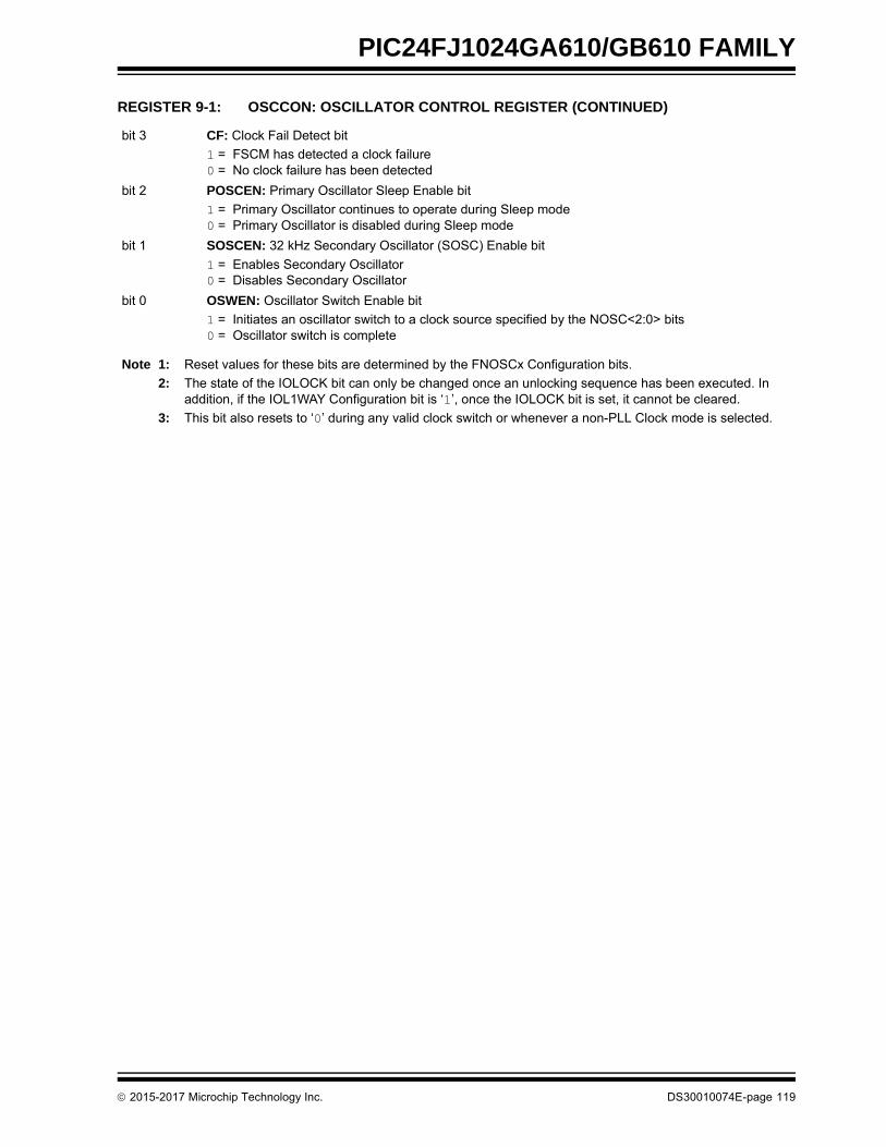
PIC24FJ1024GA610/GB610 FAMILY
bit 3 CF: Clock Fail Detect bit
1 = FSCM has detected a clock failure0 = No clock failure has been detected
bit 2 POSCEN: Primary Oscillator Sleep Enable bit
1 = Primary Oscillator continues to operate during Sleep mode0 = Primary Oscillator is disabled during Sleep mode
bit 1 SOSCEN: 32 kHz Secondary Oscillator (SOSC) Enable bit
1 = Enables Secondary Oscillator0 = Disables Secondary Oscillator
bit 0 OSWEN: Oscillator Switch Enable bit
1 = Initiates an oscillator switch to a clock source specified by the NOSC<2:0> bits0 = Oscillator switch is complete
REGISTER 9-1: OSCCON: OSCILLATOR CONTROL REGISTER (CONTINUED)
Note 1: Reset values for these bits are determined by the FNOSCx Configuration bits.
2: The state of the IOLOCK bit can only be changed once an unlocking sequence has been executed. In addition, if the IOL1WAY Configuration bit is ‘1’, once the IOLOCK bit is set, it cannot be cleared.
3: This bit also resets to ‘0’ during any valid clock switch or whenever a non-PLL Clock mode is selected.
2015-2017 Microchip Technology Inc. DS30010074E-page 119

PIC24FJ1024GA610/GB610 FAMILY
REGISTER 9-2: CLKDIV: CLOCK DIVIDER REGISTER
R/W-0 R/W-0 R/W-1 R/W-1 R/W-0 R/W-0 R/W-0 R/W-0
ROI DOZE2 DOZE1 DOZE0 DOZEN(1) RCDIV2 RCDIV1 RCDIV0
bit 15 bit 8
R/W-0 R/W-0 R/W-0 U-0 U-0 U-0 U-0 U-0
CPDIV1 CPDIV0 PLLEN — — — — —
bit 7 bit 0
Legend:
R = Readable bit W = Writable bit U = Unimplemented bit, read as ‘0’
-n = Value at POR ‘1’ = Bit is set ‘0’ = Bit is cleared x = Bit is unknown
bit 15 ROI: Recover on Interrupt bit
1 = Interrupts clear the DOZEN bit and reset the CPU peripheral clock ratio to 1:10 = Interrupts have no effect on the DOZEN bit
bit 14-12 DOZE<2:0>: CPU Peripheral Clock Ratio Select bits
111 = 1:128110 = 1:64101 = 1:32100 = 1:16011 = 1:8 (default)010 = 1:4001 = 1:2000 = 1:1
bit 11 DOZEN: Doze Enable bit(1)
1 = DOZE<2:0> bits specify the CPU peripheral clock ratio0 = CPU peripheral clock ratio is set to 1:1
bit 10-8 RCDIV<2:0>: System Frequency Divider Clock Source Select bits
000 = Fast RC Oscillator (FRC)001 = Fast RC Oscillator (FRC) with PLL module (FRCPLL)010 = Primary Oscillator (XT, HS, EC)011 = Primary Oscillator (XT, HS, EC) with PLL module (XTPLL, HSPLL, ECPLL)100 = Secondary Oscillator (SOSC)101 = Low-Power RC Oscillator (LPRC)110 = Digitally Controlled Oscillator (DCO)111 = Reserved; do not use
bit 7-6 CPDIV<1:0>: System Clock Select bits (postscaler select from 96 MHz PLL, 32 MHz clock branch)
11 = 4 MHz (divide-by-8)(2)
10 = 8 MHz (divide-by-4)(2)
01 = 16 MHz (divide-by-2)00 = 32 MHz (divide-by-1)
bit 5 PLLEN: USB PLL Enable bit
1 = PLL is always active0 = PLL is only active when a PLL Oscillator mode is selected (OSCCON<14:12> = 011 or 001)
bit 4-0 Unimplemented: Read as ‘0’
Note 1: This bit is automatically cleared when the ROI bit is set and an interrupt occurs.
2: This setting is not allowed while the USB module is enabled.
DS30010074E-page 120 2015-2017 Microchip Technology Inc.

PIC24FJ1024GA610/GB610 FAMILY
REGISTER 9-3: OSCTUN: FRC OSCILLATOR TUNE REGISTER
R/W-0 U-0 R/W-0 R/W-1 R-0 R/W-0 R-0 R/W-0
STEN — STSIDL STSRC(1) STLOCK STLPOL STOR STORPOL
bit 15 bit 8
U-0 U-0 R/W-0 R/W-0 R/W-0 R/W-0 R/W-0 R/W-0
— — TUN5(2) TUN4(2) TUN3(2) TUN2(2) TUN1(2) TUN0(2)
bit 7 bit 0
Legend:
R = Readable bit W = Writable bit U = Unimplemented bit, read as ‘0’
-n = Value at POR ‘1’ = Bit is set ‘0’ = Bit is cleared x = Bit is unknown
bit 15 STEN: FRC Self-Tune Enable bit
1 = FRC self-tuning is enabled; TUNx bits are controlled by hardware0 = FRC self-tuning is disabled; application may optionally control the TUNx bits
bit 14 Unimplemented: Read as ‘0’
bit 13 STSIDL: FRC Self-Tune Stop in Idle bit
1 = Self-tuning stops during Idle mode0 = Self-tuning continues during Idle mode
bit 12 STSRC: FRC Self-Tune Reference Clock Source bit(1)
1 = FRC is tuned to approximately match the USB host clock tolerance0 = FRC is tuned to approximately match the 32.768 kHz SOSC tolerance
bit 11 STLOCK: FRC Self-Tune Lock Status bit
1 = FRC accuracy is currently within ±0.2% of the STSRC reference accuracy0 = FRC accuracy may not be within ±0.2% of the STSRC reference accuracy
bit 10 STLPOL: FRC Self-Tune Lock Interrupt Polarity bit
1 = A self-tune lock interrupt is generated when STLOCK is ‘0’0 = A self-tune lock interrupt is generated when STLOCK is ‘1’
bit 9 STOR: FRC Self-Tune Out of Range Status bit
1 = STSRC reference clock error is beyond the range of TUN<5:0>; no tuning is performed0 = STSRC reference clock is within the tunable range; tuning is performed
bit 8 STORPOL: FRC Self-Tune Out of Range Interrupt Polarity bit
1 = A self-tune out of range interrupt is generated when STOR is ‘0’0 = A self-tune out of range interrupt is generated when STOR is ‘1’
bit 7-6 Unimplemented: Read as ‘0’
bit 5-0 TUN<5:0>: FRC Oscillator Tuning bits(2)
011111 = Maximum frequency deviation011110 = 000001 = 000000 = Center frequency, oscillator is running at factory calibrated frequency111111 = 100001 = 100000 = Minimum frequency deviation
Note 1: Use of either clock tuning reference source has specific application requirements. See Section 9.5 “FRC Active Clock Tuning” for details.
2: These bits are read-only when STEN = 1.
2015-2017 Microchip Technology Inc. DS30010074E-page 121

PIC24FJ1024GA610/GB610 FAMILY
REGISTER 9-4: DCOTUN: DIGITALLY CONTROLLED OSCILLATOR TUNE REGISTER
U-0 U-0 U-0 U-0 U-0 U-0 U-0 U-0
— — — — — — — —
bit 15 bit 8
U-0 U-0 R/W-0 R/W-0 R/W-0 R/W-0 R/W-0 R/W-0
— — DCOTUN<5:0>(1)
bit 7 bit 0
Legend:
R = Readable bit W = Writable bit U = Unimplemented bit, read as ‘0’
-n = Value at POR ‘1’ = Bit is set ‘0’ = Bit is cleared x = Bit is unknown
bit 15-6 Unimplemented: Read as ‘0’
bit 5-0 DCOTUN<5:0>: DCO Tuning bits(1)
011111 = Maximum frequency (+4.65% adjustment)011110 =• • •000001 = Increase frequency by a single step (+0.15% adjustment)000000 = Center frequency, oscillator is running at calibrated frequency111111 = Decrease frequency by a single step (-0.15% adjustment)• • •100001 =100000 = Minimum frequency (-4.80% adjustment)
Note 1: Frequency step-size will be greater for 15 MHz and 30 MHz options (±9.2% adjustment range).
DS30010074E-page 122 2015-2017 Microchip Technology Inc.
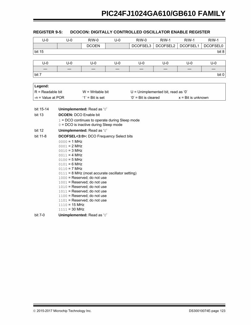
PIC24FJ1024GA610/GB610 FAMILY
REGISTER 9-5: DCOCON: DIGITALLY CONTROLLED OSCILLATOR ENABLE REGISTER
U-0 U-0 R/W-0 U-0 R/W-0 R/W-1 R/W-1 R/W-1
DCOEN DCOFSEL3 DCOFSEL2 DCOFSEL1 DCOFSEL0
bit 15 bit 8
U-0 U-0 U-0 U-0 U-0 U-0 U-0 U-0
— — — — — — — —
bit 7 bit 0
Legend:
R = Readable bit W = Writable bit U = Unimplemented bit, read as ‘0’
-n = Value at POR ‘1’ = Bit is set ‘0’ = Bit is cleared x = Bit is unknown
bit 15-14 Unimplemented: Read as ‘0’
bit 13 DCOEN: DCO Enable bit
1 = DCO continues to operate during Sleep mode0 = DCO is inactive during Sleep mode
bit 12 Unimplemented: Read as ‘0’
bit 11-8 DCOFSEL<3:0>: DCO Frequency Select bits
0000 = 1 MHz0001 = 2 MHz0010 = 3 MHz0011 = 4 MHz0100 = 5 MHz0101 = 6 MHz0110 = 7 MHz0111 = 8 MHz (most accurate oscillator setting)1000 = Reserved; do not use1001 = Reserved; do not use1010 = Reserved; do not use1011 = Reserved; do not use1100 = Reserved; do not use1101 = Reserved; do not use1110 = 15 MHz 1111 = 30 MHz
bit 7-0 Unimplemented: Read as ‘0’
2015-2017 Microchip Technology Inc. DS30010074E-page 123

PIC24FJ1024GA610/GB610 FAMILY
REGISTER 9-6: OSCDIV: OSCILLATOR DIVISOR REGISTER
U-0 R/W-0 R/W-0 R/W-0 R/W-0 R/W-0 R/W-0 R/W-0
— DIV<14:8>
bit 15 bit 8
R/W-0 R/W-0 R/W-0 R/W-0 R/W-0 R/W-0 R/W-0 R/W-1
DIV<7:0>
bit 7 bit 0
Legend:
R = Readable bit W = Writable bit U = Unimplemented bit, read as ‘0’
-n = Value at POR ‘1’ = Bit is set ‘0’ = Bit is cleared x = Bit is unknown
bit 15 Unimplemented: Read as ‘0’
bit 14-0 DIV<14:0>: Reference Clock Divider bits
Specifies the 1/2 period of the reference clock in the source clocks(ex: Period of ref_clk_output = [Reference Source * 2] * DIV<14:0>).111111111111111 = Oscillator frequency divided by 65,534 (32,767 * 2)111111111111110 = Oscillator frequency divided by 65,532 (32,766 * 2)• • •000000000000011 = Oscillator frequency divided by 6 (3 * 2)000000000000010 = Oscillator frequency divided by 4 (2 * 2)000000000000001 = Oscillator frequency divided by 2 (1 * 2) (default)000000000000000 = Oscillator frequency is unchanged (no divider)
DS30010074E-page 124 2015-2017 Microchip Technology Inc.

PIC24FJ1024GA610/GB610 FAMILY
REGISTER 9-7: OSCFDIV: OSCILLATOR FRACTIONAL DIVISOR REGISTER(1)
R/W-0 R/W-0 R/W-0 R/W-0 R/W-0 R/W-0 R/W-0 R/W-0
TRIM<0:7>
bit 15 bit 8
R/W-0 U-0 U-0 U-0 U-0 U-0 U-0 U-0
TRIM8 — — — — — — —
bit 7 bit 0
Legend:
R = Readable bit W = Writable bit U = Unimplemented bit, read as ‘0’
-n = Value at POR ‘1’ = Bit is set ‘0’ = Bit is cleared x = Bit is unknown
bit 15-7 TRIM<0:8>: Trim bits
Provides fractional additive to the DIV<14:0> value for the 1/2 period of the oscillator clock.0000_0000_0 = 0/512 (0.0) divisor added to DIVx value0000_0000_1 = 1/512 (0.001953125) divisor added to DIVx value0000_0001_0 = 2/512 (0.00390625) divisor added to DIVx value• • •100000000 = 256/512 (0.5000) divisor added to DIVx value• • •1111_1111_0 = 510/512 (0.99609375) divisor added to DIVx value1111_1111_1 = 511/512 (0.998046875) divisor added to DIVx value
bit 6-0 Unimplemented: Read as ‘0’
Note 1: TRIMx values greater than zero are ONLY valid when DIVx values are greater than zero.
2015-2017 Microchip Technology Inc. DS30010074E-page 125

PIC24FJ1024GA610/GB610 FAMILY
9.4 Clock Switching Operation
With few limitations, applications are free to switchbetween any of the five clock sources (POSC, SOSC,FRC, DCO and LPRC) under software control and atany time. To limit the possible side effects that couldresult from this flexibility, PIC24F devices have asafeguard lock built into the switching process.
9.4.1 ENABLING CLOCK SWITCHING
To enable clock switching, the FCKSM<1> Configura-tion bit in FOSC must be programmed to ‘0’. (Refer toSection 30.1 “Configuration Bits” for further details.)If the FCKSM<1> Configuration bit is unprogrammed(‘1’), the clock switching function and Fail-Safe ClockMonitor function are disabled; this is the default setting.
The NOSC<2:0> control bits (OSCCON<10:8>) donot control the clock selection when clock switchingis disabled. However, the COSC<2:0> bits(OSCCON<14:12>) will reflect the clock sourceselected by the FNOSC<2:0> Configuration bits.
The OSWEN control bit (OSCCON<0>) has no effectwhen clock switching is disabled; it is held at ‘0’ at alltimes.
9.4.2 OSCILLATOR SWITCHING SEQUENCE
At a minimum, performing a clock switch requires thisbasic sequence:
1. If desired, read the COSC<2:0> bits(OSCCON<14:12>) to determine the currentoscillator source.
2. Perform the unlock sequence to allow a write tothe OSCCON register high byte.
3. Write the appropriate value to the NOSC<2:0>bits (OSCCON<10:8>) for the new oscillatorsource.
4. Perform the unlock sequence to allow a write tothe OSCCON register low byte.
5. Set the OSWEN bit to initiate the oscillatorswitch.
Once the basic sequence is completed, the systemclock hardware responds automatically as follows:
1. The clock switching hardware compares theCOSC<2:0> bits with the new value of theNOSC<2:0> bits. If they are the same, then theclock switch is a redundant operation. In thiscase, the OSWEN bit is cleared automaticallyand the clock switch is aborted.
2. If a valid clock switch has been initiated, theLOCK (OSCCON<5>) and CF (OSCCON<3>)bits are cleared.
3. The new oscillator is turned on by the hardwareif it is not currently running. If a crystal oscillatormust be turned on, the hardware will wait untilthe OST expires. If the new source is using thePLL, then the hardware waits until a PLL lock isdetected (LOCK = 1).
4. The hardware waits for 10 clock cycles from thenew clock source and then performs the clockswitch.
5. The hardware clears the OSWEN bit to indicate asuccessful clock transition. In addition, theNOSC<2:0> bits values are transferred to theCOSC<2:0> bits.
6. The old clock source is turned off at this time,with the exception of LPRC (if WDT or FSCM isenabled) or SOSC (if SOSCEN remains set).
Note: The Primary Oscillator mode has threedifferent submodes (XT, HS and EC), whichare determined by the POSCMD<1:0>Configuration bits. While an applicationcan switch to and from Primary Oscillatormode in software, it cannot switchbetween the different primary submodeswithout reprogramming the device.
Note 1: The processor will continue to executecode throughout the clock switchingsequence. Timing-sensitive code shouldnot be executed during this time.
2: Direct clock switches between anyPrimary Oscillator mode with PLL andFRCPLL mode are not permitted. Thisapplies to clock switches in either direc-tion. In these instances, the applicationmust switch to FRC mode as a transi-tional clock source between the two PLLmodes.
DS30010074E-page 126 2015-2017 Microchip Technology Inc.

PIC24FJ1024GA610/GB610 FAMILY
A recommended code sequence for a clock switchincludes the following:
1. Disable interrupts during the OSCCON registerunlock and write sequence.
2. Execute the unlock sequence for the OSCCONhigh byte by writing 78h and 9Ah toOSCCON<15:8> in two back-to-back instructions.
3. Write the new oscillator source to the NOSCxbits in the instruction immediately following theunlock sequence.
4. Execute the unlock sequence for the OSCCONlow byte by writing 46h and 57h toOSCCON<7:0> in two back-to-back instructions.
5. Set the OSWEN bit in the instruction immediatelyfollowing the unlock sequence.
6. Continue to execute code that is not clock-sensitive(optional).
7. Invoke an appropriate amount of software delay(cycle counting) to allow the selected oscillatorand/or PLL to start and stabilize.
8. Check to see if OSWEN is ‘0’. If it is, the switchwas successful. If OSWEN is still set, thencheck the LOCK bit to determine the cause ofthe failure.
The core sequence for unlocking the OSCCON registerand initiating a clock switch is shown in Example 9-1.
EXAMPLE 9-1: BASIC CODE SEQUENCE FOR CLOCK SWITCHING
9.5 FRC Active Clock Tuning
PIC24FJ1024GA610/GB610 family devices include anautomatic mechanism to calibrate the FRC during runtime. This system uses active clock tuning from a sourceof known accuracy to maintain the FRC within a verynarrow margin of its nominal 8 MHz frequency. Thisallows for a frequency accuracy that is well within therequirements of the “USB 2.0 Specification” regardingfull-speed USB devices.
The self-tune system is controlled by the bits in the upperhalf of the OSCTUN register. Setting the STEN bit(OSCTUN<15>) enables the self-tuning feature, allow-ing the hardware to calibrate to a source selected by theSTSRC bit (OSCTUN<12>). When STSRC = 1, thesystem uses the Start-of-Frame (SOF) packets from anexternal USB host for its source. When STSRC = 0, thesystem uses the crystal-controlled SOSC for its calibra-tion source. Regardless of the source, the system usesthe TUN<5:0> bits (OSCTUN<5:0>) to change the FRCOscillator’s frequency. Frequency monitoring andadjustment is dynamic, occurring continuously duringrun time. While the system is active, the TUNx bitscannot be written to by software.
The self-tune system can generate a hardware interrupt,FSTIF. The interrupt can result from a drift of the FRCfrom the reference, by greater than 0.2% in either direc-tion, or whenever the frequency deviation is beyondthe ability of the TUN<5:0> bits to correct (i.e.,greater than 1.5%). The STLOCK and STOR statusbits (OSCTUN<11,9>) are used to indicate theseconditions.
The STLPOL and STORPOL bits (OSCTUN<10,8>)configure the FSTIF interrupt to occur in the presenceor the absence of the conditions. It is the user’s respon-sibility to monitor both the STLOCK and STOR bits todetermine the exact cause of the interrupt.
;Place the new oscillator selection in W0;OSCCONH (high byte) Unlock SequenceMOV #OSCCONH, w1MOV #0x78, w2MOV #0x9A, w3MOV.b w2, [w1]MOV.b w3, [w1];Set new oscillator selectionMOV.b WREG, OSCCONH;OSCCONL (low byte) unlock sequenceMOV #OSCCONL, w1MOV #0x46, w2MOV #0x57, w3MOV.b w2, [w1]MOV.b w3, [w1];Start oscillator switch operationBSET OSCCON, #0
Note: The self-tune feature maintains sufficientaccuracy for operation in USB Devicemode. For applications that function as aUSB host, a high-accuracy clock source(±0.05%) is still required.
Note: To use the USB as a reference clock tuningsource (STSRC = 1), the microcontrollermust be configured for USB device opera-tion and connected to a non-suspendedUSB host or hub port.
If the SOSC is to be used as the referenceclock tuning source (STSRC = 0), theSOSC must also be enabled for clocktuning to occur.
Note: The STLPOL and STORPOL bits shouldbe ignored when the self-tune system isdisabled (STEN = 0).
2015-2017 Microchip Technology Inc. DS30010074E-page 127

PIC24FJ1024GA610/GB610 FAMILY
9.6 PLL Oscillator Modes and USB Operation
The PLL block, shown in Figure 9-2, can generate awide range of clocks used for both parts with USB func-tionality (PIC24FJ1024GB610 family) and non-USBfunctionality (PIC24FJ1024GA610 family). All of theavailable PLL modes are available for both familieswhether or nor USB is enabled or present.
The PLL input clock source (FRC or POSC) is controlledby the COSC<2:0> bits (OSCCON<14:12>) if the PLLoutput is used as a system clock. WhenCOSC<2:0> = 001 (FRCPLL), the PLL is clocked fromFRC, and when COSC<2:0> = 011 (PRIPLL), thePrimary Oscillator (POSC) is connected to the PLL.The default COSC<2:0> value is selected by theFNOSC<2:0> Configuration bits (FOSCSEL<2:0>).Also, REFO can use the PLL when it is not selected forthe system clock (COSC<2:0> bits (OSCCON<14:12>)are not ‘001’ or ‘011’). In this case, the PLL clocksource is selected by the PLLSS Configuration bit(FOSC<4>). If PLLSS is cleared (‘0’), the PLL is fed bythe FRC Oscillator. If the PLLSS Configuration bit is notprogrammed (‘1’), the PLL is clocked from the PrimaryOscillator.
When used in a USB application, the 48 MHz internalclock must be running at all times which requires theVCO of the PLL to run at 96 MHz. This, in turn, forcesthe system clock (that drives the CPU and peripherals)to route the 96 MHz through a fixed divide-by-3 block(generating 32 MHz) and then through a selection offour fixed divisors (‘postscaler’). The postscaler outputbecomes the system clock.
The input to the PLL must be 4 MHz when used in a USBapplication, which restricts the frequency input sourcesto be used with a small set of fixed frequency dividers(see Figure 9-2). For example, if a 12 MHz crystal isused, the PLLMODE<3:0> Configuration bits must beset for divide-by-3 to generate the required 4 MHz. Apopular baud rate crystal is 11.0592 MHz, but this valuecannot be used for USB operation as there are no divi-sors available to generate 4 MHz exactly. See Table 9-3for the possible combinations of input clock andPLLMODE<3:0> bits settings for USB operation.
Non-USB operation allows a wider range of PLL inputfrequencies. The multiplier ratios can be selected as4x, 6x or 8x and there is no clock prescaler. Thepostscaler (CPDIV<1:0>) is available and can be usedto reduce the system clock to meet the 32 MHzmaximum specification. Note that the minimum inputfrequency to the PLL is 2 MHz, but the range is 2 MHzto 8 MHz. Therefore, it is possible to select a multiplierratio that exceeds the 32 MHz maximum specificationfor the system clock. This allows the system clock to beany frequency between 8 MHz (2 MHz input clock with4x multiplier ratio) and 32 MHz (4 MHz input clock with8x multiplier ratio). For example, a common crystalfrequency is 3.58 MHz (‘color burst’) and this can be
used with the 6x multiplier to generate a system clockof 21.48 MHz. The VCO frequency becomes thesystem clock.
The PLL block is shown in Figure 9-2. In this system, thePLL input is divided down by a PLL prescaler to generatea 4 MHz output. This is used to drive an on-chip, 96 MHzPLL frequency multiplier to drive the two clock branches.One branch uses a fixed, divide-by-2 frequency divider togenerate the 48 MHz USB clock. The other branch usesa fixed, divide-by-3 frequency divider and configurablePLL prescaler/divider to generate a range of systemclock frequencies. The CPDIV<1:0> bits select thesystem clock speed. The available clock options arelisted in Table 9-2.
The USB PLL prescaler must be configured to generatethe required 4 MHz VCO input using the PLLMODE<3:0>Configuration bits. This limits the choices for the PLLsource frequency to a total of 8 possibilities, as shown inTable 9-3.
TABLE 9-2: SYSTEM CLOCK OPTIONS DURING USB OPERATION
TABLE 9-3: VALID PRIMARY OSCILLATOR CONFIGURATIONS FOR USB OPERATIONS(1)
Note 1: The maximum operating frequency of thesystem clock is 32 MHz. It is up to theuser to select the proper multiplier ratiowith the selected clock source frequency.
Clock Division(CPDIV<1:0>)
Microcontroller OscillatorClock Frequency (FOSC)
None (00) 32 MHz
2 (01) 16 MHz
4 (10)(1) 8 MHz
8 (11)(1) 4 MHz
Note 1: System clock frequencies below 16 MHz are too slow to allow USB operation. The USB module must be disabled to use this option. See Section 9.6.1 “Considerations for USB Operation”.
PLL Input Frequency
Clock ModePLL Mode
(PLLMODE<3:0>)
48 MHz EC 12 (0111)
32 MHz HS, EC 8 (0110)
24 MHz HS, EC 6 (0101)
20 MHz HS, EC 5 (0100)
16 MHz HS, EC 4 (0011)
12 MHz HS, EC 3 (0010)
8 MHz EC, XT, FRC(2) 2 (0001)
4 MHz EC, XT 1 (0000)
Note 1: USB operation restricts the VCO input frequency to be 4 MHz.
2: This requires the use of the FRC self-tune feature to maintain the required clock accuracy.
DS30010074E-page 128 2015-2017 Microchip Technology Inc.

PIC24FJ1024GA610/GB610 FAMILY
FIGURE 9-2: PLL BLOCK
PLL
Pre
sca
ler
4 MHz
CP
UD
ivid
er
48 MHz Clock for USB Module
PLL Output forSystem Clock and REFO
CPDIV<1:0>
PLLMODE<3:0>(1)
POSC
FRC
32 MHz
01110110010101000011001000010000
12
8
8 6 5 4 3 2 1
4
2
1 00
01
10
11
Note 1: The FNOSC<2:0>, PLLMODE<3:0> and PLLSS bits are in the configuration area. See the FOSC and FOSCSEL Configuration registers (Register 30-6 and Register 30-7) for more information.
1100
1101
1110x8
x6
x4
2
3
8 MHz-32 MHz
USB
COSC<2:0>/FNOSC<2:0> = 001 (FRCPLL),COSC<2:0>/FNOSC<2:0> = 011 (PRIPLL),otherwise PLLSS bit (FOSC<4>) for REFO(1)
96 MHzPLL
2 MHz-8 MHz
2015-2017 Microchip Technology Inc. DS30010074E-page 129

PIC24FJ1024GA610/GB610 FAMILY
9.6.1 CONSIDERATIONS FOR USB OPERATION
When using the USB On-The-Go module inPIC24FJ1024GA610/GB610 devices, users must alwaysobserve these rules in configuring the system clock:
• The system clock frequency must be 16 MHz or 32 MHz. System clock frequencies below 16 MHz are not allowed for USB module operation.
• The Oscillator modes listed in Table 9-3 are the only oscillator configurations that permit USB operation. There is no provision to provide a separate external clock source to the USB module.
• For USB operation, the selected clock source (EC, HS or XT) must meet the USB clock tolerance requirements.
• When the FRCPLL Oscillator mode is used for USB applications, the FRC self-tune system should be used as well. While the FRC is accurate, the only two ways to ensure the level of accuracy, required by the “USB 2.0 Specification” throughout the appli-cation’s operating range, are either the self-tune system or manually changing the TUN<5:0> bits.
• The user must always ensure that the FRC source is configured to provide a frequency of 4 MHz or 8 MHz (RCDIV<2:0> = 001 or 000) and that the USB PLL prescaler is configured appropriately.
• All other Oscillator modes are available; however, USB operation is not possible when these modes are selected. They may still be useful in cases where other power levels of operation are desirable and the USB module is not needed (e.g., the application is Sleeping and waiting for a bus attachment).
9.7 Reference Clock Output
In addition to the CLKO output (FOSC/2), thePIC24FJ1024GA610/GB610 family devices can be con-figured to provide a reference clock output signal to a portpin. This feature is available in all oscillator configurationsand allows the user to select a greater range of clock sub-multiples to drive external devices in the application.CLKO is enabled by Configuration bit, OSCIOFCN, andis independent of the REFO reference clock. REFO ismappable to any I/O pin that has mapped outputcapability. Refer to Table 11-4 for more information. TheREFO module block diagram is shown on Figure 9-3.
FIGURE 9-3: REFERENCE CLOCK GENERATOR
REFO
OE
To SPI,RODIV<14:0>
ROTRIM<0:8>REFI PinPLL (4/6/8X OR 96 MHZ)
SOSCLPRC
POSCPeripheral Clock
ROSEL<3:0>
CCP, CLCOscillator Clock
FRCDivider
10000110010101000011001000010000
DS30010074E-page 130 2015-2017 Microchip Technology Inc.
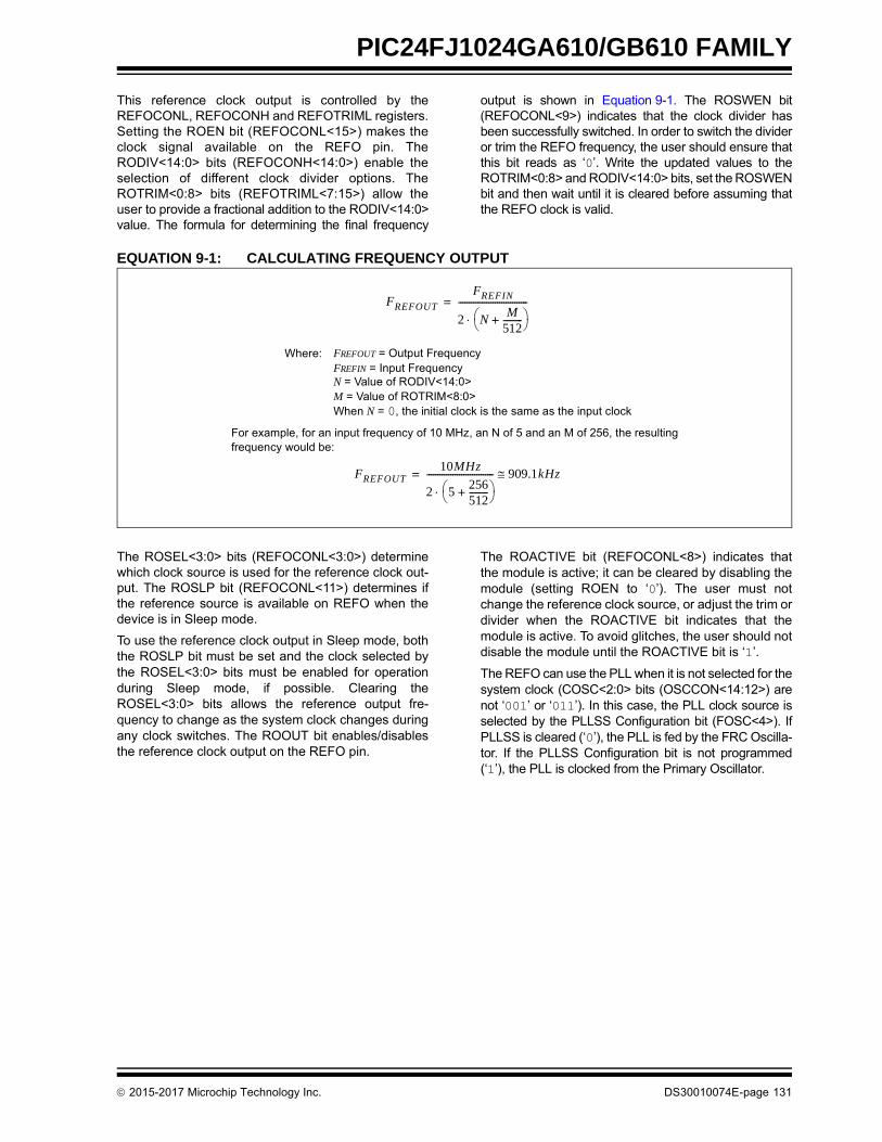
PIC24FJ1024GA610/GB610 FAMILY
This reference clock output is controlled by theREFOCONL, REFOCONH and REFOTRIML registers.Setting the ROEN bit (REFOCONL<15>) makes theclock signal available on the REFO pin. TheRODIV<14:0> bits (REFOCONH<14:0>) enable theselection of different clock divider options. TheROTRIM<0:8> bits (REFOTRIML<7:15>) allow theuser to provide a fractional addition to the RODIV<14:0>value. The formula for determining the final frequency
output is shown in Equation 9-1. The ROSWEN bit(REFOCONL<9>) indicates that the clock divider hasbeen successfully switched. In order to switch the divideror trim the REFO frequency, the user should ensure thatthis bit reads as ‘0’. Write the updated values to theROTRIM<0:8> and RODIV<14:0> bits, set the ROSWENbit and then wait until it is cleared before assuming thatthe REFO clock is valid.
EQUATION 9-1: CALCULATING FREQUENCY OUTPUT
The ROSEL<3:0> bits (REFOCONL<3:0>) determinewhich clock source is used for the reference clock out-put. The ROSLP bit (REFOCONL<11>) determines ifthe reference source is available on REFO when thedevice is in Sleep mode.
To use the reference clock output in Sleep mode, boththe ROSLP bit must be set and the clock selected bythe ROSEL<3:0> bits must be enabled for operationduring Sleep mode, if possible. Clearing theROSEL<3:0> bits allows the reference output fre-quency to change as the system clock changes duringany clock switches. The ROOUT bit enables/disablesthe reference clock output on the REFO pin.
The ROACTIVE bit (REFOCONL<8>) indicates thatthe module is active; it can be cleared by disabling themodule (setting ROEN to ‘0’). The user must notchange the reference clock source, or adjust the trim ordivider when the ROACTIVE bit indicates that themodule is active. To avoid glitches, the user should notdisable the module until the ROACTIVE bit is ‘1’.
The REFO can use the PLL when it is not selected for thesystem clock (COSC<2:0> bits (OSCCON<14:12>) arenot ‘001’ or ‘011’). In this case, the PLL clock source isselected by the PLLSS Configuration bit (FOSC<4>). IfPLLSS is cleared (‘0’), the PLL is fed by the FRC Oscilla-tor. If the PLLSS Configuration bit is not programmed(‘1’), the PLL is clocked from the Primary Oscillator.
FREFOUT
FREFIN
2 NM
512---------+
--------------------------------=
Where:
N = Value of RODIV<14:0>M = Value of ROTRIM<8:0>When N = 0, the initial clock is the same as the input clock
FREFOUT = Output FrequencyFREFIN = Input Frequency
For example, for an input frequency of 10 MHz, an N of 5 and an M of 256, the resultingfrequency would be:
FREFOUT10MHz
2 5256512---------+
------------------------------- 909.1kHz=
2015-2017 Microchip Technology Inc. DS30010074E-page 131

PIC24FJ1024GA610/GB610 FAMILY
9.8 Secondary Oscillator
9.8.1 BASIC SOSC OPERATION
PIC24FJ1024GA610/GB610 family devices do not haveto set the SOSCEN bit to use the Secondary Oscillator.Any module requiring the SOSC (such as RTCC orTimer1) will automatically turn on the SOSC when theclock signal is needed. The SOSC, however, has a longstart-up time (as long as 1 second). To avoid delays forperipheral start-up, the SOSC can be manually startedusing the SOSCEN bit.
To use the Secondary Oscillator, the SOSCSEL bit(FOSC<3>) must be set to ‘1’. Programming theSOSCSEL bit to ‘0’ configures the SOSC pins for Digitalmode, enabling digital I/O functionality on the pins.
9.8.2 CRYSTAL SELECTION
The 32.768 kHz crystal used for the SOSC must havethe following specifications in order to properly start upand run at the correct frequency when in High-Powermode:
• 12.5 pF loading capacitance• 1.0 pF shunt capacitance• A typical ESR of 35K; 50K maximum
In addition, the two external crystal loading capacitorsshould be in the range of 18-22 pF, which will be basedon the PC board layout. The capacitors should be C0G,5% tolerance and rated 25V or greater.
The accuracy and duty cycle of the SOSC can bemeasured on the REFO pin, and is recommended to bein the range of 40-60% and accurate to ±0.65 Hz.
9.8.3 LOW-POWER SOSC OPERATION
The Secondary Oscillator can operate in two distinctlevels of power consumption based on device configu-ration. In Low-Power mode, the oscillator operates in alow drive strength, low-power state. By default, theoscillator uses a higher drive strength, and therefore,requires more power. Low-Power mode is selected byConfiguration bit, SOSCHP (FDEVOPT1<3>). Thelower drive strength of this mode makes the SOSCmore sensitive to noise and requires a longer start-uptime. This mode can be used with lower load capaci-tance crystals (6 pF-9 pF) having higher ESR ratings(50K-80K) to reduce Sleep current in the RTCC. WhenLow-Power mode is used, care must be taken in thedesign and layout of the SOSC circuit to ensure that theoscillator starts up and oscillates properly. PC boardlayout issues, stray capacitance and other factors willneed to be carefully controlled in order for the crystal tooperate.
DS30010074E-page 132 2015-2017 Microchip Technology Inc.
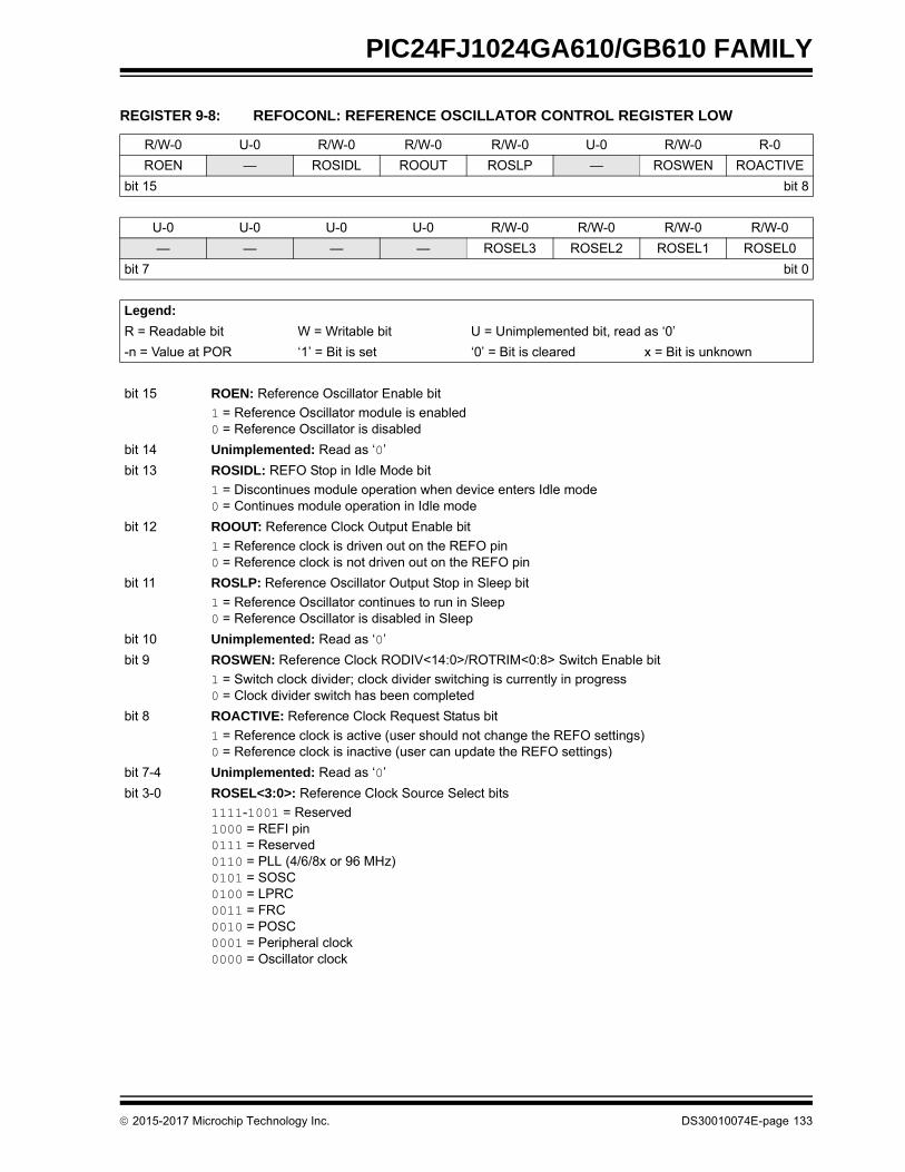
PIC24FJ1024GA610/GB610 FAMILY
REGISTER 9-8: REFOCONL: REFERENCE OSCILLATOR CONTROL REGISTER LOW
R/W-0 U-0 R/W-0 R/W-0 R/W-0 U-0 R/W-0 R-0
ROEN — ROSIDL ROOUT ROSLP — ROSWEN ROACTIVE
bit 15 bit 8
U-0 U-0 U-0 U-0 R/W-0 R/W-0 R/W-0 R/W-0
— — — — ROSEL3 ROSEL2 ROSEL1 ROSEL0
bit 7 bit 0
Legend:
R = Readable bit W = Writable bit U = Unimplemented bit, read as ‘0’
-n = Value at POR ‘1’ = Bit is set ‘0’ = Bit is cleared x = Bit is unknown
bit 15 ROEN: Reference Oscillator Enable bit
1 = Reference Oscillator module is enabled0 = Reference Oscillator is disabled
bit 14 Unimplemented: Read as ‘0’
bit 13 ROSIDL: REFO Stop in Idle Mode bit
1 = Discontinues module operation when device enters Idle mode0 = Continues module operation in Idle mode
bit 12 ROOUT: Reference Clock Output Enable bit
1 = Reference clock is driven out on the REFO pin0 = Reference clock is not driven out on the REFO pin
bit 11 ROSLP: Reference Oscillator Output Stop in Sleep bit
1 = Reference Oscillator continues to run in Sleep0 = Reference Oscillator is disabled in Sleep
bit 10 Unimplemented: Read as ‘0’
bit 9 ROSWEN: Reference Clock RODIV<14:0>/ROTRIM<0:8> Switch Enable bit
1 = Switch clock divider; clock divider switching is currently in progress0 = Clock divider switch has been completed
bit 8 ROACTIVE: Reference Clock Request Status bit
1 = Reference clock is active (user should not change the REFO settings)0 = Reference clock is inactive (user can update the REFO settings)
bit 7-4 Unimplemented: Read as ‘0’
bit 3-0 ROSEL<3:0>: Reference Clock Source Select bits
1111-1001 = Reserved1000 = REFI pin0111 = Reserved0110 = PLL (4/6/8x or 96 MHz)0101 = SOSC0100 = LPRC0011 = FRC0010 = POSC0001 = Peripheral clock0000 = Oscillator clock
2015-2017 Microchip Technology Inc. DS30010074E-page 133

PIC24FJ1024GA610/GB610 FAMILY
REGISTER 9-9: REFOCONH: REFERENCE OSCILLATOR CONTROL REGISTER HIGH
U-0 R/W-0 R/W-0 R/W-0 R/W-0 R/W-0 R/W-0 R/W-0
— RODIV<14:8>
bit 15 bit 8
R/W-0 R/W-0 R/W-0 R/W-0 R/W-0 R/W-0 R/W-0 R/W-0
RODIV<7:0>
bit 7 bit 0
Legend:
R = Readable bit W = Writable bit U = Unimplemented bit, read as ‘0’
-n = Value at POR ‘1’ = Bit is set ‘0’ = Bit is cleared x = Bit is unknown
bit 15 Unimplemented: Read as ‘0’
bit 14-0 RODIV<14:0>: Reference Clock Divider bits
Specifies 1/2 period of the reference clock in the source clocks(ex: Period of Output = [Reference Source * 2] * RODIV<14:0>; this equation does not apply to RODIV<14:0> = 0).111111111111111 = REFO clock is the base clock frequency divided by 65,534 (32,767 * 2)111111111111110 = REFO clock is the base clock frequency divided by 65,532 (32,766 * 2)•••000000000000011 = REFO clock is the base clock frequency divided by 6 (3 * 2)000000000000010 = REFO clock is the base clock frequency divided by 4 (2 * 2)000000000000001 = REFO clock is the base clock frequency divided by 2 (1 * 2)000000000000000 = REFO clock is the same frequency as the base clock (no divider)
DS30010074E-page 134 2015-2017 Microchip Technology Inc.

PIC24FJ1024GA610/GB610 FAMILY
REGISTER 9-10: REFOTRIML: REFERENCE OSCILLATOR TRIM REGISTER LOW
R/W-0 R/W-0 R/W-0 R/W-0 R/W-0 R/W-0 R/W-0 R/W-0
ROTRIM<0:7>
bit 15 bit 8
R/W-0 U-0 U-0 U-0 U-0 U-0 U-0 U-0
ROTRIM8 — — — — — — —
bit 7 bit 0
Legend:
R = Readable bit W = Writable bit U = Unimplemented bit, read as ‘0’
-n = Value at POR ‘1’ = Bit is set ‘0’ = Bit is cleared x = Bit is unknown
bit 15-7 ROTRIM<0:8>: REFO Trim bits
These bits provide a fractional additive to the RODIV<14:0> value for the 1/2 period of the REFO clock.000000000 = 0/512 (0.0 divisor added to the RODIV<14:0> value)000000001 = 1/512 (0.001953125 divisor added to the RODIV<14:0> value)000000010 = 2/512 (0.00390625 divisor added to the RODIV<14:0> value)•••100000000 = 256/512 (0.5000 divisor added to the RODIV<14:0> value)•••111111110 = 510/512 (0.99609375 divisor added to the RODIV<14:0> value)111111111 = 511/512 (0.998046875 divisor added to the RODIV<14:0> value)
bit 6-0 Unimplemented: Read as ‘0’
2015-2017 Microchip Technology Inc. DS30010074E-page 135

PIC24FJ1024GA610/GB610 FAMILY
NOTES:
DS30010074E-page 136 2015-2017 Microchip Technology Inc.

PIC24FJ1024GA610/GB610 FAMILY
10.0 POWER-SAVING FEATURES
The PIC24FJ1024GA610/GB610 family of devicesprovides the ability to manage power consumption byselectively managing clocking to the CPU and theperipherals. In general, a lower clock frequency and areduction in the number of circuits being clocked con-stitutes lower consumed power. All PIC24F devicesmanage power consumption in four different ways:
• Clock Frequency
• Instruction-Based Sleep and Idle modes
• Software-Controlled Doze mode
• Selective Peripheral Control in Software
Combinations of these methods can be used toselectively tailor an application’s power consumption,while still maintaining critical application features, suchas timing-sensitive communications.
10.1 Clock Frequency and Clock Switching
PIC24F devices allow for a wide range of clockfrequencies to be selected under application control. Ifthe system clock configuration is not locked, users canchoose low-power or high-precision oscillators by simplychanging the NOSC<2:0> bits. The process of changinga system clock during operation, as well as limitations tothe process, are discussed in more detail in Section 9.0“Oscillator Configuration”.
10.2 Instruction-Based Power-Saving Modes
PIC24F devices have two special power-saving modesthat are entered through the execution of a specialPWRSAV instruction. Sleep mode stops clock operationand halts all code execution; Idle mode halts the CPU
and code execution, but allows peripheral modules tocontinue operation. The assembly syntax of thePWRSAV instruction is shown in Example 10-1.
The XC16 C compiler offers “built-in” functions for thepower-saving modes as follows:
Idle(); // places part in Idle
Sleep(); // places part in Sleep
Sleep and Idle modes can be exited as a result of anenabled interrupt, WDT time-out or a device Reset. Whenthe device exits these modes, it is said to “wake-up”.
10.2.1 SLEEP MODE
Sleep mode has these features:
• The system clock source is shut down. If an on-chip oscillator is used, it is turned off.
• The device current consumption will be reduced to a minimum provided that no I/O pin is sourcing current.
• The Fail-Safe Clock Monitor does not operate during Sleep mode since the system clock source is disabled.
• The LPRC clock will continue to run in Sleep mode if the WDT is enabled.
• The WDT, if enabled, is automatically cleared prior to entering Sleep mode.
• Some device features or peripherals may continue to operate in Sleep mode. This includes items, such as the Input Change Notification (ICN) on the I/O ports or peripherals that use an external clock input. Any peripheral that requires the system clock source for its operation will be disabled in Sleep mode.
The device will wake-up from Sleep mode on any of thethese events:
• On any interrupt source that is individually enabled
• On any form of device Reset
• On a WDT time-out
On wake-up from Sleep, the processor will restart withthe same clock source that was active when Sleepmode was entered.
EXAMPLE 10-1: PWRSAV INSTRUCTION SYNTAX
Note: This data sheet summarizes the featuresof this group of PIC24F devices. It is notintended to be a comprehensive refer-ence source. For more information, referto the “dsPIC33/PIC24 Family ReferenceManual”, “Power-Saving Features”(DS39698), which is available from theMicrochip web site (www.microchip.com).The information in this data sheetsupersedes the information in the FRM.
Note: SLEEP_MODE and IDLE_MODE are con-stants defined in the assembler includefile for the selected device.
PWRSAV #SLEEP_MODE ; Put the device into SLEEP modePWRSAV #IDLE_MODE ; Put the device into IDLE mode
2015-2017 Microchip Technology Inc. DS30010074E-page 137
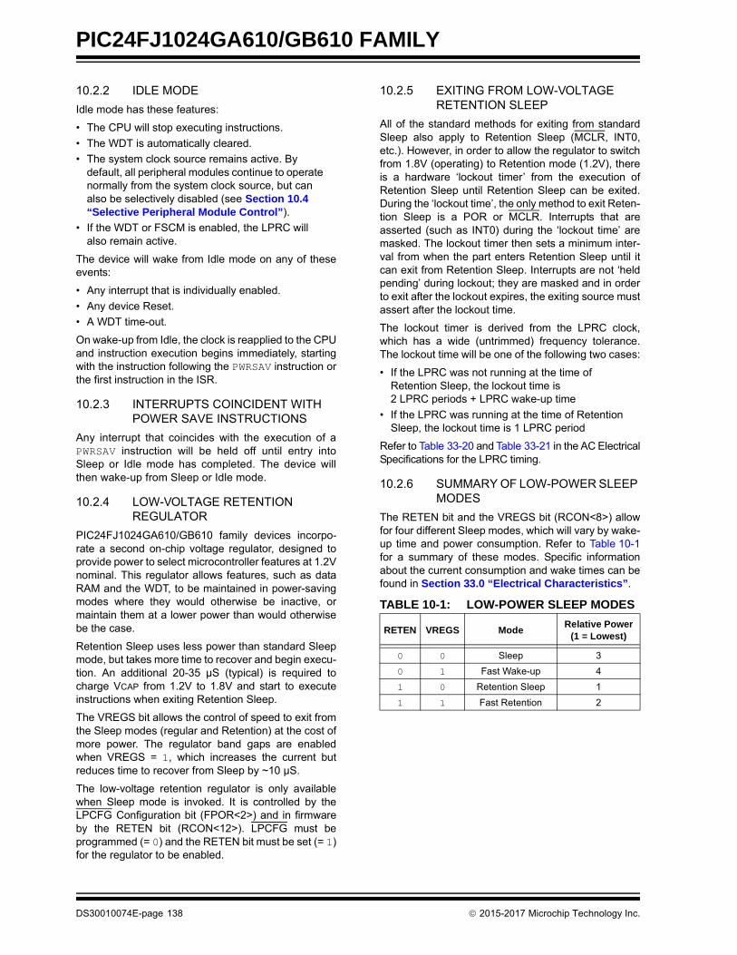
PIC24FJ1024GA610/GB610 FAMILY
10.2.2 IDLE MODE
Idle mode has these features:
• The CPU will stop executing instructions.
• The WDT is automatically cleared.
• The system clock source remains active. By default, all peripheral modules continue to operate normally from the system clock source, but can also be selectively disabled (see Section 10.4 “Selective Peripheral Module Control”).
• If the WDT or FSCM is enabled, the LPRC will also remain active.
The device will wake from Idle mode on any of theseevents:
• Any interrupt that is individually enabled.
• Any device Reset.
• A WDT time-out.
On wake-up from Idle, the clock is reapplied to the CPUand instruction execution begins immediately, startingwith the instruction following the PWRSAV instruction orthe first instruction in the ISR.
10.2.3 INTERRUPTS COINCIDENT WITH POWER SAVE INSTRUCTIONS
Any interrupt that coincides with the execution of aPWRSAV instruction will be held off until entry intoSleep or Idle mode has completed. The device willthen wake-up from Sleep or Idle mode.
10.2.4 LOW-VOLTAGE RETENTION REGULATOR
PIC24FJ1024GA610/GB610 family devices incorpo-rate a second on-chip voltage regulator, designed toprovide power to select microcontroller features at 1.2Vnominal. This regulator allows features, such as dataRAM and the WDT, to be maintained in power-savingmodes where they would otherwise be inactive, ormaintain them at a lower power than would otherwisebe the case.
Retention Sleep uses less power than standard Sleepmode, but takes more time to recover and begin execu-tion. An additional 20-35 µS (typical) is required tocharge VCAP from 1.2V to 1.8V and start to executeinstructions when exiting Retention Sleep.
The VREGS bit allows the control of speed to exit fromthe Sleep modes (regular and Retention) at the cost ofmore power. The regulator band gaps are enabledwhen VREGS = 1, which increases the current butreduces time to recover from Sleep by ~10 µS.
The low-voltage retention regulator is only availablewhen Sleep mode is invoked. It is controlled by theLPCFG Configuration bit (FPOR<2>) and in firmwareby the RETEN bit (RCON<12>). LPCFG must beprogrammed (= 0) and the RETEN bit must be set (= 1)for the regulator to be enabled.
10.2.5 EXITING FROM LOW-VOLTAGE RETENTION SLEEP
All of the standard methods for exiting from standardSleep also apply to Retention Sleep (MCLR, INT0,etc.). However, in order to allow the regulator to switchfrom 1.8V (operating) to Retention mode (1.2V), thereis a hardware ‘lockout timer’ from the execution ofRetention Sleep until Retention Sleep can be exited.During the ‘lockout time’, the only method to exit Reten-tion Sleep is a POR or MCLR. Interrupts that areasserted (such as INT0) during the ‘lockout time’ aremasked. The lockout timer then sets a minimum inter-val from when the part enters Retention Sleep until itcan exit from Retention Sleep. Interrupts are not ‘heldpending’ during lockout; they are masked and in orderto exit after the lockout expires, the exiting source mustassert after the lockout time.
The lockout timer is derived from the LPRC clock,which has a wide (untrimmed) frequency tolerance.The lockout time will be one of the following two cases:
• If the LPRC was not running at the time of Retention Sleep, the lockout time is 2 LPRC periods + LPRC wake-up time
• If the LPRC was running at the time of Retention Sleep, the lockout time is 1 LPRC period
Refer to Table 33-20 and Table 33-21 in the AC ElectricalSpecifications for the LPRC timing.
10.2.6 SUMMARY OF LOW-POWER SLEEP MODES
The RETEN bit and the VREGS bit (RCON<8>) allowfor four different Sleep modes, which will vary by wake-up time and power consumption. Refer to Table 10-1for a summary of these modes. Specific informationabout the current consumption and wake times can befound in Section 33.0 “Electrical Characteristics”.
TABLE 10-1: LOW-POWER SLEEP MODES
RETEN VREGS ModeRelative Power
(1 = Lowest)
0 0 Sleep 3
0 1 Fast Wake-up 4
1 0 Retention Sleep 1
1 1 Fast Retention 2
DS30010074E-page 138 2015-2017 Microchip Technology Inc.

PIC24FJ1024GA610/GB610 FAMILY
10.3 Doze Mode
Generally, changing clock speed and invoking one ofthe power-saving modes are the preferred strategiesfor reducing power consumption. There may becircumstances, however, where this is not practical. Forexample, it may be necessary for an application tomaintain uninterrupted synchronous communication,even while it is doing nothing else. Reducing systemclock speed may introduce communication errors,while using a power-saving mode may stopcommunications completely.
Doze mode is a simple and effective alternative methodto reduce power consumption while the device is stillexecuting code. In this mode, the system clock contin-ues to operate from the same source and at the samespeed. Peripheral modules continue to be clocked atthe same speed while the CPU clock speed is reduced.Synchronization between the two clock domains ismaintained, allowing the peripherals to access theSFRs while the CPU executes code at a slower rate.
Doze mode is enabled by setting the DOZEN bit(CLKDIV<11>). The ratio between peripheral and coreclock speed is determined by the DOZE<2:0> bits(CLKDIV<14:12>). There are eight possibleconfigurations, from 1:1 to 1:256, with 1:1 being thedefault.
It is also possible to use Doze mode to selectivelyreduce power consumption in event driven applica-tions. This allows clock-sensitive functions, such assynchronous communications, to continue withoutinterruption while the CPU Idles, waiting for somethingto invoke an interrupt routine. Enabling the automaticreturn to full-speed CPU operation on interrupts isenabled by setting the ROI bit (CLKDIV<15>). Bydefault, interrupt events have no effect on Doze modeoperation.
10.4 Selective Peripheral Module Control
Idle and Doze modes allow users to substantiallyreduce power consumption by slowing or stopping theCPU clock. Even so, peripheral modules still remainclocked, and thus, consume power. There may becases where the application needs what these modesdo not provide: the allocation of power resources toCPU processing with minimal power consumption fromthe peripherals.
PIC24F devices address this requirement by allowingperipheral modules to be selectively disabled, reducingor eliminating their power consumption. This can bedone with two control bits:
• The Peripheral Enable bit, generically named, “XXXEN”, located in the module’s main control SFR.
• The Peripheral Module Disable (PMD) bit, generically named, “XXXMD”, located in one of the PMD Control registers.
Both bits have similar functions in enabling or disablingtheir associated module. Setting the PMD bit for amodule disables all clock sources to that module,reducing its power consumption to an absolute mini-mum. In this state, the control and status registersassociated with the peripheral will also be disabled, sowrites to those registers will have no effect and readvalues will be invalid. Many peripheral modules have acorresponding PMD bit.
In contrast, disabling a module by clearing its XXXENbit disables its functionality, but leaves its registersavailable to be read and written to. This reduces powerconsumption, but not by as much as setting the PMDbit does. Most peripheral modules have an enable bit;exceptions include input capture, output compare andRTCC.
To achieve more selective power savings, peripheralmodules can also be selectively disabled when thedevice enters Idle mode. This is done through thecontrol bit of the generic name format, “XXXIDL”. Bydefault, all modules that can operate during Idle modewill do so. Using the disable on Idle feature allowsfurther reduction of power consumption during Idlemode, enhancing power savings for extremely criticalpower applications.
2015-2017 Microchip Technology Inc. DS30010074E-page 139

PIC
24F
J102
4GA
610/G
B6
10 F
AM
ILY
DS
30
01
00
74
E-p
ag
e 1
40
2
01
5-2
01
7 M
icroch
ip T
ech
no
log
y Inc.
Bit 3 Bit 2 Bit 1 Bit 0All
Resets
SPI1MD — — ADCMD 0000
OC4MD OC3MD OC2MD OC1MD 0000
U3MD I2C3MD I2C2MD — 0000
REFOMD CTMUMD LVDMD USBMD(1) 0000
CCP4MD CCP3MD CCP2MD CCP1MD 0000
— — — SPI3MD 0000
— — — — 0000
CLC2MD CLC1MD — — 0000
TABLE 10-2: PERIPHERAL MODULE DISABLE REGISTER SUMMARY
Register Bit 15 Bit 14 Bit 13 Bit 12 Bit 11 Bit 10 Bit 9 Bit 8 Bit 7 Bit 6 Bit 5 Bit 4
PMD1 T5MD T4MD T3MD T2MD T1MD — — — I2C1MD U2MD U1MD SPI2MD
PMD2 — — IC6MD IC5MD IC4MD IC3MD IC2MD IC1MD — — OC6MD OC5MD
PMD3 — — — — — CMPMD RTCCMD PMPMD CRCMD — — —
PMD4 — — — — — — — — — — U4MD —
PMD5 — — — — — — — — — CCP7MD CCP6MD CCP5MD
PMD6 — — — — — — — — — — — —
PMD7 — — — — — — — — — — DMA1MD DMA0MD
PMD8 — — — — — — — — U6MD U5MD CLC4MD CLC3MD
Legend: — = unimplemented, read as ‘0’. Reset values are shown in hexadecimal.
Note 1: USB is not present on PIC24FJXXXXGA6XX devices.

PIC24FJ1024GA610/GB610 FAMILY
REGISTER 10-1: PMD1: PERIPHERAL MODULE DISABLE REGISTER 1
R/W-0 R/W-0 R/W-0 R/W-0 R/W-0 U-0 U-0 U-0
T5MD T4MD T3MD T2MD T1MD — — —
bit 15 bit 8
R/W-0 R/W-0 R/W-0 R/W-0 R/W-0 U-0 U-0 R/W-0
I2C1MD U2MD U1MD SPI2MD SPI1MD — — ADC1MD
bit 7 bit 0
Legend:
R = Readable bit W = Writable bit U = Unimplemented bit, read as ‘0’
-n = Value at POR ‘1’ = Bit is set ‘0’ = Bit is cleared x = Bit is unknown
bit 15 T5MD: Timer5 Module Disable bit
1 = Module is disabled0 = Module power and clock sources are enabled
bit 14 T4MD: Timer4 Module Disable bit
1 = Module is disabled0 = Module power and clock sources are enabled
bit 13 T3MD: Timer3 Module Disable bit
1 = Module is disabled0 = Module power and clock sources are enabled
bit 12 T2MD: Timer2 Module Disable bit
1 = Module is disabled0 = Module power and clock sources are enabled
bit 11 T1MD: Timer1 Module Disable bit
1 = Module is disabled0 = Module power and clock sources are enabled
bit 10-8 Unimplemented: Read as ‘0’
bit 7 I2C1MD: I2C1 Module Disable bit
1 = Module is disabled0 = Module power and clock sources are enabled
bit 6 U2MD: UART2 Module Disable bit
1 = Module is disabled0 = Module power and clock sources are enabled
bit 5 U1MD: UART1 Module Disable bit
1 = Module is disabled0 = Module power and clock sources are enabled
bit 4 SPI2MD: SPI2 Module Disable bit
1 = Module is disabled0 = Module power and clock sources are enabled
bit 3 SPI1MD: SPI1 Module Disable bit
1 = Module is disabled0 = Module power and clock sources are enabled
bit 2-1 Unimplemented: Read as ‘0’
bit 0 ADC1MD: A/D Converter Module Disable bit
1 = Module is disabled0 = Module power and clock sources are enabled
2015-2017 Microchip Technology Inc. DS30010074E-page 141

PIC24FJ1024GA610/GB610 FAMILY
REGISTER 10-2: PMD2: PERIPHERAL MODULE DISABLE REGISTER 2
U-0 U-0 R/W-0 R/W-0 R/W-0 R/W-0 R/W-0 R/W-0
— — IC6MD IC5MD IC4MD IC3MD IC2MD IC1MD
bit 15 bit 8
U-0 U-0 R/W-0 R/W-0 R/W-0 R/W-0 R/W-0 R/W-0
— — OC6MD OC5MD OC4MD OC3MD OC2MD OC1MD
bit 7 bit 0
Legend:
R = Readable bit W = Writable bit U = Unimplemented bit, read as ‘0’
-n = Value at POR ‘1’ = Bit is set ‘0’ = Bit is cleared x = Bit is unknown
bit 15-14 Unimplemented: Read as ‘0’
bit 13 IC6MD: Input Capture 6 Module Disable bit
1 = Module is disabled0 = Module power and clock sources are enabled
bit 12 IC5MD: Input Capture 5 Module Disable bit
1 = Module is disabled0 = Module power and clock sources are enabled
bit 11 IC4MD: Input Capture 4 Module Disable bit
1 = Module is disabled0 = Module power and clock sources are enabled
bit 10 IC3MD: Input Capture 3 Module Disable bit
1 = Module is disabled0 = Module power and clock sources are enabled
bit 9 IC2MD: Input Capture 2 Module Disable bit
1 = Module is disabled0 = Module power and clock sources are enabled
bit 8 IC1MD: Input Capture 1 Module Disable bit
1 = Module is disabled0 = Module power and clock sources are enabled
bit 7-6 Unimplemented: Read as ‘0’
bit 5 OC6MD: Output Capture 6 Module Disable bit
1 = Module is disabled0 = Module power and clock sources are enabled
bit 4 OC5MD: Output Capture 5 Module Disable bit
1 = Module is disabled0 = Module power and clock sources are enabled
bit 3 OC4MD: Output Capture 4 Module Disable bit
1 = Module is disabled0 = Module power and clock sources are enabled
bit 2 OC3MD: Output Capture 3 Module Disable bit
1 = Module is disabled0 = Module power and clock sources are enabled
bit 1 OC2MD: Output Capture 2 Module Disable bit
1 = Module is disabled0 = Module power and clock sources are enabled
bit 0 OC1MD: Output Capture 1 Module Disable bit
1 = Module is disabled0 = Module power and clock sources are enabled
DS30010074E-page 142 2015-2017 Microchip Technology Inc.

PIC24FJ1024GA610/GB610 FAMILY
REGISTER 10-3: PMD3: PERIPHERAL MODULE DISABLE REGISTER 3
U-0 U-0 U-0 U-0 U-0 R/W-0 R/W-0 R/W-0
— — — — — CMPMD RTCCMD PMPMD
bit 15 bit 8
R/W-0 U-0 U-0 U-0 R/W-0 R/W-0 R/W-0 U-0
CRCMD — — — U3MD I2C3MD I2C2MD —
bit 7 bit 0
Legend:
R = Readable bit W = Writable bit U = Unimplemented bit, read as ‘0’
-n = Value at POR ‘1’ = Bit is set ‘0’ = Bit is cleared x = Bit is unknown
bit 15-11 Unimplemented: Read as ‘0’
bit 10 CMPMD: Triple Comparator Module Disable bit
1 = Module is disabled0 = Module power and clock sources are enabled
bit 9 RTCCMD: RTCC Module Disable bit
1 = Module is disabled0 = Module power and clock sources are enabled
bit 8 PMPMD: Enhanced Parallel Master Port Disable bit
1 = Module is disabled0 = Module power and clock sources are enabled
bit 7 CRCMD: CRC Module Disable bit
1 = Module is disabled0 = Module power and clock sources are enabled
bit 6-4 Unimplemented: Read as ‘0’
bit 3 U3MD: UART3 Module Disable bit
1 = Module is disabled0 = Module power and clock sources are enabled
bit 2 I2C3MD: I2C3 Module Disable bit
1 = Module is disabled0 = Module power and clock sources are enabled
bit 1 I2C2MD: I2C2 Module Disable bit
1 = Module is disabled0 = Module power and clock sources are enabled
bit 0 Unimplemented: Read as ‘0’
2015-2017 Microchip Technology Inc. DS30010074E-page 143
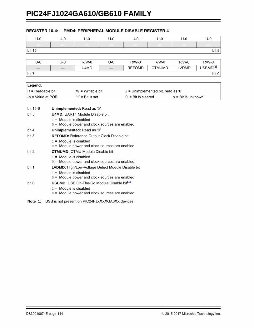
PIC24FJ1024GA610/GB610 FAMILY
REGISTER 10-4: PMD4: PERIPHERAL MODULE DISABLE REGISTER 4
U-0 U-0 U-0 U-0 U-0 U-0 U-0 U-0
— — — — — — — —
bit 15 bit 8
U-0 U-0 R/W-0 U-0 R/W-0 R/W-0 R/W-0 R/W-0
— — U4MD — REFOMD CTMUMD LVDMD USBMD(1)
bit 7 bit 0
Legend:
R = Readable bit W = Writable bit U = Unimplemented bit, read as ‘0’
-n = Value at POR ‘1’ = Bit is set ‘0’ = Bit is cleared x = Bit is unknown
bit 15-6 Unimplemented: Read as ‘0’
bit 5 U4MD: UART4 Module Disable bit
1 = Module is disabled0 = Module power and clock sources are enabled
bit 4 Unimplemented: Read as ‘0’
bit 3 REFOMD: Reference Output Clock Disable bit
1 = Module is disabled0 = Module power and clock sources are enabled
bit 2 CTMUMD: CTMU Module Disable bit
1 = Module is disabled0 = Module power and clock sources are enabled
bit 1 LVDMD: High/Low-Voltage Detect Module Disable bit
1 = Module is disabled0 = Module power and clock sources are enabled
bit 0 USBMD: USB On-The-Go Module Disable bit(1)
1 = Module is disabled0 = Module power and clock sources are enabled
Note 1: USB is not present on PIC24FJXXXXGA6XX devices.
DS30010074E-page 144 2015-2017 Microchip Technology Inc.
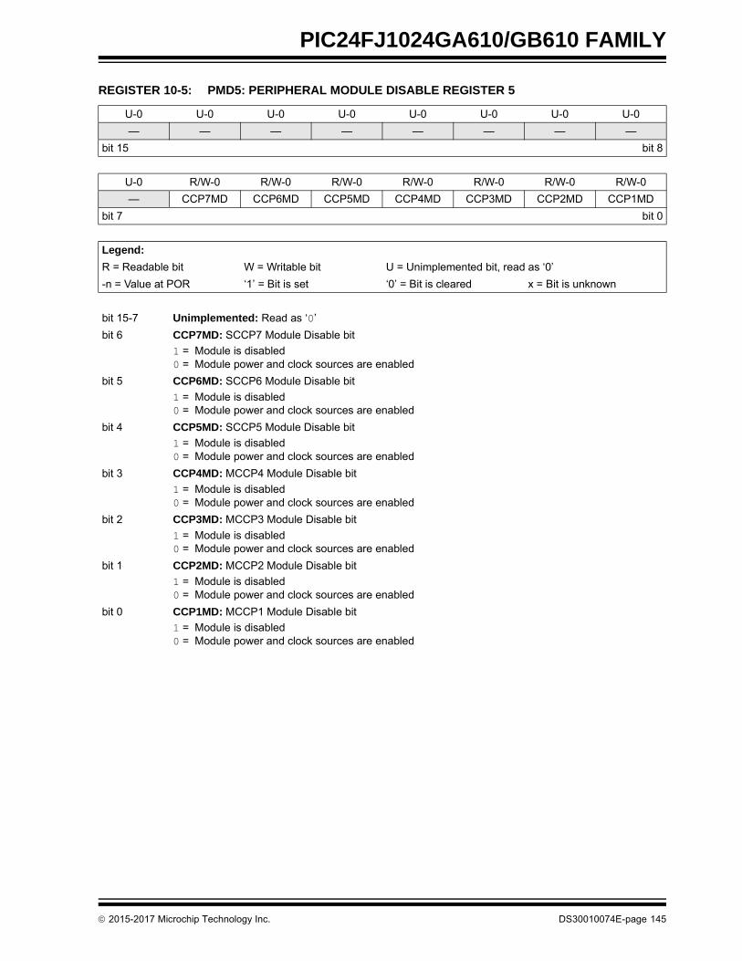
PIC24FJ1024GA610/GB610 FAMILY
REGISTER 10-5: PMD5: PERIPHERAL MODULE DISABLE REGISTER 5
U-0 U-0 U-0 U-0 U-0 U-0 U-0 U-0
— — — — — — — —
bit 15 bit 8
U-0 R/W-0 R/W-0 R/W-0 R/W-0 R/W-0 R/W-0 R/W-0
— CCP7MD CCP6MD CCP5MD CCP4MD CCP3MD CCP2MD CCP1MD
bit 7 bit 0
Legend:
R = Readable bit W = Writable bit U = Unimplemented bit, read as ‘0’
-n = Value at POR ‘1’ = Bit is set ‘0’ = Bit is cleared x = Bit is unknown
bit 15-7 Unimplemented: Read as ‘0’
bit 6 CCP7MD: SCCP7 Module Disable bit
1 = Module is disabled0 = Module power and clock sources are enabled
bit 5 CCP6MD: SCCP6 Module Disable bit
1 = Module is disabled0 = Module power and clock sources are enabled
bit 4 CCP5MD: SCCP5 Module Disable bit
1 = Module is disabled0 = Module power and clock sources are enabled
bit 3 CCP4MD: MCCP4 Module Disable bit
1 = Module is disabled0 = Module power and clock sources are enabled
bit 2 CCP3MD: MCCP3 Module Disable bit
1 = Module is disabled0 = Module power and clock sources are enabled
bit 1 CCP2MD: MCCP2 Module Disable bit
1 = Module is disabled0 = Module power and clock sources are enabled
bit 0 CCP1MD: MCCP1 Module Disable bit
1 = Module is disabled0 = Module power and clock sources are enabled
2015-2017 Microchip Technology Inc. DS30010074E-page 145

PIC24FJ1024GA610/GB610 FAMILY
REGISTER 10-6: PMD6: PERIPHERAL MODULE DISABLE REGISTER 6
U-0 U-0 U-0 U-0 U-0 U-0 U-0 U-0
— — — — — — — —
bit 15 bit 8
U-0 U-0 U-0 U-0 U-0 U-0 U-0 R/W-0
— — — — — — — SPI3MD
bit 7 bit 0
Legend:
R = Readable bit W = Writable bit U = Unimplemented bit, read as ‘0’
-n = Value at POR ‘1’ = Bit is set ‘0’ = Bit is cleared x = Bit is unknown
bit 15-1 Unimplemented: Read as ‘0’
bit 0 SPI3MD: SPI3 Module Disable bit
1 = Module is disabled0 = Module power and clock sources are enabled
REGISTER 10-7: PMD7: PERIPHERAL MODULE DISABLE REGISTER 7
U-0 U-0 U-0 U-0 U-0 U-0 U-0 U-0
— — — — — — — —
bit 15 bit 8
U-0 U-0 R/W-0 R/W-0 U-0 U-0 U-0 U-0
— — DMA1MD DMA0MD — — — —
bit 7 bit 0
Legend:
R = Readable bit W = Writable bit U = Unimplemented bit, read as ‘0’
-n = Value at POR ‘1’ = Bit is set ‘0’ = Bit is cleared x = Bit is unknown
bit 15-6 Unimplemented: Read as ‘0’
bit 5 DMA1MD: DMA1 Controller (Channels 4 through 7) Disable bit
1 = Controller is disabled0 = Controller power and clock sources are enabled
bit 4 DMA0MD: DMA0 Controller (Channels 0 through 3) Disable bit
1 = Controller is disabled0 = Controller power and clock sources are enabled
bit 3-0 Unimplemented: Read as ‘0’
DS30010074E-page 146 2015-2017 Microchip Technology Inc.
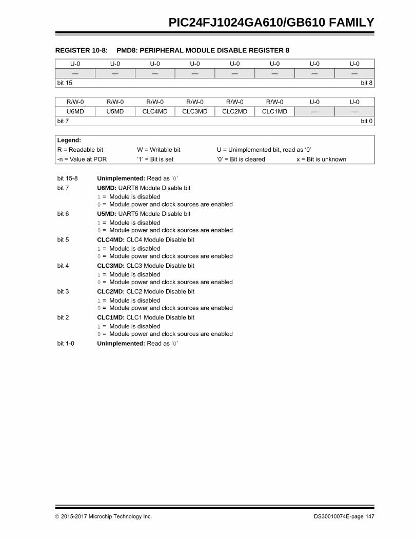
PIC24FJ1024GA610/GB610 FAMILY
REGISTER 10-8: PMD8: PERIPHERAL MODULE DISABLE REGISTER 8
U-0 U-0 U-0 U-0 U-0 U-0 U-0 U-0
— — — — — — — —
bit 15 bit 8
R/W-0 R/W-0 R/W-0 R/W-0 R/W-0 R/W-0 U-0 U-0
U6MD U5MD CLC4MD CLC3MD CLC2MD CLC1MD — —
bit 7 bit 0
Legend:
R = Readable bit W = Writable bit U = Unimplemented bit, read as ‘0’
-n = Value at POR ‘1’ = Bit is set ‘0’ = Bit is cleared x = Bit is unknown
bit 15-8 Unimplemented: Read as ‘0’
bit 7 U6MD: UART6 Module Disable bit
1 = Module is disabled0 = Module power and clock sources are enabled
bit 6 U5MD: UART5 Module Disable bit
1 = Module is disabled0 = Module power and clock sources are enabled
bit 5 CLC4MD: CLC4 Module Disable bit
1 = Module is disabled0 = Module power and clock sources are enabled
bit 4 CLC3MD: CLC3 Module Disable bit
1 = Module is disabled0 = Module power and clock sources are enabled
bit 3 CLC2MD: CLC2 Module Disable bit
1 = Module is disabled0 = Module power and clock sources are enabled
bit 2 CLC1MD: CLC1 Module Disable bit
1 = Module is disabled0 = Module power and clock sources are enabled
bit 1-0 Unimplemented: Read as ‘0’
2015-2017 Microchip Technology Inc. DS30010074E-page 147

PIC24FJ1024GA610/GB610 FAMILY
NOTES:
DS30010074E-page 148 2015-2017 Microchip Technology Inc.

PIC24FJ1024GA610/GB610 FAMILY
2015-2017 Microchip Technology Inc. DS30010074E-page 149
11.0 I/O PORTS
All of the device pins (except power and reset) areshared between the peripherals and the Parallel I/O(PIO) ports. All I/O input ports feature Schmitt Trigger(ST) inputs for improved noise immunity.
11.1 Parallel I/O (PIO) Ports
A Parallel I/O port that shares a pin with a peripheral is,in general, subservient to the peripheral. The periph-eral’s output buffer data and control signals areprovided to a pair of multiplexers. The multiplexersselect whether the peripheral or the associated porthas ownership of the output data and control signals ofthe I/O pin. The logic also prevents “loop through”, inwhich a port’s digital output can drive the input of a
peripheral that shares the same pin. Figure 11-1 showshow ports are shared with other peripherals and theassociated I/O pin to which they are connected.
When a peripheral is enabled and the peripheral isactively driving an associated pin, the use of the pin as ageneral purpose output pin is disabled. The I/O pin maybe read, but the output driver for the parallel port bit will bedisabled. If a peripheral is enabled, but the peripheral isnot actively driving a pin, that pin may be driven by a port.
All port pins have three registers directly associatedwith their operation as digital I/Os and one registerassociated with their operation as analog inputs. TheData Direction register (TRISx) determines whether thepin is an input or an output. If the data direction bit is a‘1’, then the pin is an input. All port pins are defined asinputs after a Reset. Reads from the Output Latchregister (LATx), read the latch; writes to the latch, writethe latch. Reads from the PORTx register, read the portpins; writes to the port pins, write the latch.
Any bit and its associated data and control registersthat are not valid for a particular device will bedisabled. That means the corresponding LATx andTRISx registers, and the port pin, will read as zeros.
When a pin is shared with another peripheral or func-tion that is defined as an input only, it is regarded as adedicated port because there is no other competingsource of inputs.
FIGURE 11-1: BLOCK DIAGRAM OF A TYPICAL SHARED PORT STRUCTURE
Note: This data sheet summarizes the features ofthis group of PIC24F devices. It is notintended to be a comprehensive referencesource. For more information, refer tothe “dsPIC33/PIC24 Family ReferenceManual”, “I/O Ports with Interrupt-on-Change (IOC)” (DS70005186), which isavailable from the Microchip web site(www.microchip.com). The information inthis data sheet supersedes the informationin the FRM.
QD
CK
WR LAT +
TRIS Latch
I/O Pin
WR PORT
Data Bus
QD
CK
Data Latch
Read PORT
Read TRIS
1
0
1
0
WR TRIS
Peripheral Output DataOutput Enable
Peripheral Input Data
I/O
Peripheral Module
Peripheral Output Enable
PIO Module
Output Multiplexers
Output Data
Input Data
Peripheral Module Enable
Read LAT

PIC24FJ1024GA610/GB610 FAMILY
11.1.1 I/O PORT WRITE/READ TIMING
One instruction cycle is required between a portdirection change or port write operation and a readoperation of the same port. Typically, this instructionwould be a NOP.
11.1.2 OPEN-DRAIN CONFIGURATION
In addition to the PORTx, LATx and TRISx registers fordata control, each port pin can also be individuallyconfigured for either a digital or open-drain output. Thisis controlled by the Open-Drain Control register, ODCx,associated with each port. Setting any of the bits con-figures the corresponding pin to act as an open-drainoutput.
The open-drain feature allows the generation ofoutputs higher than VDD (e.g., 5V) on any desireddigital only pins by using external pull-up resistors. Themaximum open-drain voltage allowed is the same asthe maximum VIH specification.
11.2 Configuring Analog Port Pins (ANSx)
The ANSx and TRISx registers control the operation ofthe pins with analog function. Each port pin with analogfunction is associated with one of the ANSx bits (seeRegister 11-1 through Register 11-6), which decides ifthe pin function should be analog or digital. Refer toTable 11-1 for detailed behavior of the pin for differentANSx and TRISx bit settings.
When reading the PORTx register, all pins configured asanalog input channels will read as cleared (a low level).
11.2.1 ANALOG INPUT PINS AND VOLTAGE CONSIDERATIONS
The voltage tolerance of pins used as device inputs isdependent on the pin’s input function. Most input pinsare able to handle DC voltages of up to 5.5V, a level typ-ical for digital logic circuits. However, several pins canonly tolerate voltages up to VDD. Voltage excursionsbeyond VDD on these pins should always be avoided.
Table 11-2 summarizes the different voltage toler-ances. For more information, refer to Section 33.0“Electrical Characteristics” for more details.
TABLE 11-1: CONFIGURING ANALOG/DIGITAL FUNCTION OF AN I/O PIN
Pin Function ANSx Setting TRISx Setting Comments
Analog Input 1 1 It is recommended to keep ANSx = 1.
Analog Output 1 1 It is recommended to keep ANSx = 1.
Digital Input 0 1 Firmware must wait at least one instruction cycle after configuring a pin as a digital input before a valid input value can be read.
Digital Output 0 0 Make sure to disable the analog output function on the pin if any is present.
TABLE 11-2: INPUT VOLTAGE LEVELS FOR PORT OR PIN TOLERATED DESCRIPTION INPUT
Port or Pin Tolerated Input Description
PORTA<15:14,5:0>
5.5VTolerates input levels above VDD; useful for most standard logic.
PORTC<3:1>
PORTD<15:8,5:0>
PORTE<8:5,3:0>
PORTF<13:12,8:0>
PORTG<15:12,1:0>
PORTA<10:9,7:6>
VDD Only VDD input levels are tolerated.
PORTB<15:0>
PORTC<15:13,4>(1)
PORTD<7:6>
PORTE<9,4>
PORTG<9:6,3:2>(2)
Note 1: PORTC<12> has OSCI pin function.
2: PORTG<3:2> have USB function on PIC24FJXXXXGBXXX devices.
DS30010074E-page 150 2015-2017 Microchip Technology Inc.

PIC24FJ1024GA610/GB610 FAMILY
REGISTER 11-1: ANSA: PORTA ANALOG FUNCTION SELECTION REGISTER
U-0 U-0 U-0 U-0 U-0 R/W-1 R/W-1 U-0
— — — — — ANSA<10:9>(1) —
bit 15 bit 8
R/W-1 R/W-1 U-0 U-0 U-0 U-0 U-0 U-0
ANSA<7:6>(1) — — — — — —
bit 7 bit 0
Legend:
R = Readable bit W = Writable bit U = Unimplemented bit, read as ‘0’
-n = Value at POR ‘1’ = Bit is set ‘0’ = Bit is cleared x = Bit is unknown
bit 15-11 Unimplemented: Read as ‘0’
bit 10-9 ANSA<10:9>: PORTA Analog Function Selection bits(1)
1 = Pin is configured in Analog mode; I/O port read is disabled0 = Pin is configured in Digital mode; I/O port read is enabled
bit 8 Unimplemented: Read as ‘0’
bit 7-6 ANSA<7:6>: PORTA Analog Function Selection bits(1)
1 = Pin is configured in Analog mode; I/O port read is disabled0 = Pin is configured in Digital mode; I/O port read is enabled
bit 5-0 Unimplemented: Read as ‘0’
Note 1: ANSA<10:9,7> bits are not available on 64-pin devices.
REGISTER 11-2: ANSB: PORTB ANALOG FUNCTION SELECTION REGISTER
R/W-1 R/W-1 R/W-1 R/W-1 R/W-1 R/W-1 R/W-1 R/W-1
ANSB<15:8>
bit 15 bit 8
R/W-1 R/W-1 R/W-1 R/W-1 R/W-1 R/W-1 R/W-1 R/W-1
ANSB<7:0>
bit 7 bit 0
Legend:
R = Readable bit W = Writable bit U = Unimplemented bit, read as ‘0’
-n = Value at POR ‘1’ = Bit is set ‘0’ = Bit is cleared x = Bit is unknown
bit 15-0 ANSB<15:0>: PORTB Analog Function Selection bits
1 = Pin is configured in Analog mode; I/O port read is disabled0 = Pin is configured in Digital mode; I/O port read is enabled
2015-2017 Microchip Technology Inc. DS30010074E-page 151

PIC24FJ1024GA610/GB610 FAMILY
REGISTER 11-3: ANSC: PORTC ANALOG FUNCTION SELECTION REGISTER
U-0 R/W-1 R/W-1 U-0 U-0 U-0 U-0 U-0
— ANSC<14:13> — — — — —
bit 15 bit 8
U-0 U-0 U-0 R/W-1 U-0 U-0 U-0 U-0
— — — ANSC4(1) — — — —
bit 7 bit 0
Legend:
R = Readable bit W = Writable bit U = Unimplemented bit, read as ‘0’
-n = Value at POR ‘1’ = Bit is set ‘0’ = Bit is cleared x = Bit is unknown
bit 15 Unimplemented: Read as ‘0’
bit 14-13 ANSC<14:13>: PORTC Analog Function Selection bits
1 = Pin is configured in Analog mode; I/O port read is disabled0 = Pin is configured in Digital mode; I/O port read is enabled
bit 12-5 Unimplemented: Read as ‘0’
bit 4 ANSC4: PORTC Analog Function Selection bit(1)
1 = Pin is configured in Analog mode; I/O port read is disabled0 = Pin is configured in Digital mode; I/O port read is enabled
bit 3-0 Unimplemented: Read as ‘0’
Note 1: ANSC4 is not available on 64-pin devices.
REGISTER 11-4: ANSD: PORTD ANALOG FUNCTION SELECTION REGISTER
U-0 U-0 r-1 U-0 U-0 U-0 U-0 U-0
— — — — — — — —
bit 15 bit 8
R/W-1 R/W-1 U-0 U-0 U-0 U-0 U-0 U-0
ANSD<7:6> — — — — — —
bit 7 bit 0
Legend: r = Reserved bit
R = Readable bit W = Writable bit U = Unimplemented bit, read as ‘0’
-n = Value at POR ‘1’ = Bit is set ‘0’ = Bit is cleared x = Bit is unknown
bit 15-14 Unimplemented: Read as ‘0’
bit 13 Reserved: Read as ‘1’
bit 12-8 Unimplemented: Read as ‘0’
bit 7-6 ANSD<7:6>: PORTD Analog Function Selection bits
1 = Pin is configured in Analog mode; I/O port read is disabled0 = Pin is configured in Digital mode; I/O port read is enabled
bit 5-0 Unimplemented: Read as ‘0’
DS30010074E-page 152 2015-2017 Microchip Technology Inc.

PIC24FJ1024GA610/GB610 FAMILY
REGISTER 11-5: ANSE: PORTE ANALOG FUNCTION SELECTION REGISTER
U-0 U-0 U-0 U-0 U-0 U-0 R/W-1 U-0
— — — — — — ANSE9(1) —
bit 15 bit 8
U-0 U-0 U-0 R/W-1 U-0 U-0 U-0 U-0
— — — ANSE4 — — — —
bit 7 bit 0
Legend:
R = Readable bit W = Writable bit U = Unimplemented bit, read as ‘0’
-n = Value at POR ‘1’ = Bit is set ‘0’ = Bit is cleared x = Bit is unknown
bit 15-10 Unimplemented: Read as ‘0’
bit 9 ANSE9: PORTE Analog Function Selection bit(1)
1 = Pin is configured in Analog mode; I/O port read is disabled0 = Pin is configured in Digital mode; I/O port read is enabled
bit 8-5 Unimplemented: Read as ‘0’
bit 4 ANSE4: PORTE Analog Function Selection bit
1 = Pin is configured in Analog mode; I/O port read is disabled0 = Pin is configured in Digital mode; I/O port read is enabled
bit 3-0 Unimplemented: Read as ‘0’
Note 1: ANSE9 is not available on 64-pin devices.
REGISTER 11-6: ANSG: PORTG ANALOG FUNCTION SELECTION REGISTER
U-0 U-0 U-0 U-0 U-0 U-0 R/W-1 R/W-1
— — — — — — ANSG<9:8>
bit 15 bit 8
R/W-1 R/W-1 U-0 U-0 U-0 U-0 U-0 U-0
ANSG<7:6> — — — — — —
bit 7 bit 0
Legend:
R = Readable bit W = Writable bit U = Unimplemented bit, read as ‘0’
-n = Value at POR ‘1’ = Bit is set ‘0’ = Bit is cleared x = Bit is unknown
bit 15-10 Unimplemented: Read as ‘0’
bit 9-6 ANSG<9:6>: PORTG Analog Function Selection bits
1 = Pin is configured in Analog mode; I/O port read is disabled0 = Pin is configured in Digital mode; I/O port read is enabled
bit 5-0 Unimplemented: Read as ‘0’
2015-2017 Microchip Technology Inc. DS30010074E-page 153

PIC24FJ1024GA610/GB610 FAMILY
11.3 Interrupt-on-Change (IOC)
The Interrupt-on-Change function of the I/O portsallows the PIC24FJ1024GA610/GB610 family ofdevices to generate interrupt requests to the processorin response to a Change-of-State (COS) on selectedinput pins. This feature is capable of detecting inputChange-of-States, even in Sleep mode when theclocks are disabled.
Interrupt-on-Change functionality is enabled on a pinby setting the IOCPx and/or IOCNx register bit for thatpin. For example, PORTC has register names, IOCPCand IOCNC, for these functions. Setting a value of ‘1’ inthe IOCPx register enables interrupts for low-to-hightransitions, while setting a value of ‘1’ in the IOCNxregister enables interrupts for high-to-low transitions.Setting a value of ‘1’ in both register bits will enableinterrupts for either case (e.g., a pulse on the pin willgenerate two interrupts). In order for any IOC to bedetected, the global IOC Interrupt Enable bit (IEC1<3>)must be set, the IOCON bit (PADCON<15>) set and theassociated IFSx flag cleared.
When an interrupt request is generated for a pin, thecorresponding status flag (IOCFx register bit) will beset, indicating that a Change-of-State occurred on thatpin. The IOCFx register bit will remain set until clearedby writing a zero to it. When any IOCFx flag bit in agiven port is set, the corresponding IOCPxF bit in theIOCSTAT register will be set. This flag indicates that achange was detected on one of the bits on the givenport. The IOCPxF flag will be cleared when allIOCFx<15:0> bits are cleared.
Multiple individual status flags can be cleared by writinga zero to one or more bits using a Read-Modify-Writeoperation. If another edge is detected on a pin whosestatus bit is being cleared during the Read-Modify-Write sequence, the associated change flag will still beset at the end of the Read-Modify-Write sequence.
The user should use the instruction sequence (orequivalent) shown in Example 11-1 to clear theInterrupt-on-Change Status registers.
At the end of this sequence, the W0 register will containa zero for each bit for which the port pin had a changedetected. In this way, any indication of a pin changingwill not be lost.
Due to the asynchronous and real-time nature of theInterrupt-on-Change, the value read on the port pinsmay not indicate the state of the port when the changewas detected, as a second change can occur duringthe interval between clearing the flag and reading theport. It is up to the user code to handle this case if it isa possibility in their application. To keep this interval toa minimum, it is recommended that any code modifyingthe IOCFx registers be run either in the interrupthandler or with interrupts disabled.
Each Interrupt-on-Change (IOC) pin has both a weakpull-up and a weak pull-down connected to it. The pull-ups act as a current source connected to the pin, whilethe pull-downs act as a current sink connected to thepin. These eliminate the need for external resistorswhen push button or keypad devices are connected.
The pull-ups and pull-downs are separately enabledusing the IOCPUx registers (for pull-ups) and theIOCPDx registers (for pull-downs). Each IOC pin hasindividual control bits for its pull-up and pull-down. Set-ting a control bit enables the weak pull-up or pull-downfor the corresponding pin.
EXAMPLE 11-1: IOC STATUS READ/CLEAR IN ASSEMBLY
EXAMPLE 11-2: PORT READ/WRITE IN ASSEMBLY
EXAMPLE 11-3: PORT READ/WRITE IN ‘C’
Note: Pull-ups and pull-downs on pins shouldalways be disabled whenever the pin isconfigured as a digital output.
MOV 0xFFFF, W0 ; Initial mask value 0xFFFF -> W0XOR IOCFx, W0 ; W0 has '1' for each bit set in IOCFxAND IOCFx ; IOCFx & W0 ->IOCFx
MOV 0xFF00, W0 ; Configure PORTB<15:8> as inputsMOV W0, TRISB ; and PORTB<7:0> as outputsNOP ; Delay 1 cycleBTSS PORTB, #13 ; Next Instruction
TRISB = 0xFF00; // Configure PORTB<15:8> as inputs and PORTB<7:0> as outputsNop(); // Delay 1 cycleIf (PORTBbits.RB13) ; // Test if RB13 is a ‘1’
DS30010074E-page 154 2015-2017 Microchip Technology Inc.

PIC24FJ1024GA610/GB610 FAMILY
REGISTER 11-7: PADCON: PORT CONFIGURATION REGISTER
R/W-0 U-0 U-0 U-0 U-0 U-0 U-0 U-0
IOCON — — — — — — —
bit 15 bit 8
U-0 U-0 U-0 U-0 U-0 U-0 U-0 R/W-0
— — — — — — — PMPTTL
bit 7 bit 0
Legend:
R = Readable bit W = Writable bit U = Unimplemented bit, read as ‘0’
-n = Value at POR ‘1’ = Bit is set ‘0’ = Bit is cleared x = Bit is unknown
bit 15 IOCON: Interrupt-on-Change Enable bit
1 = Interrupt-on-Change functionality is enabled0 = Interrupt-on-Change functionality is disabled
bit 14-1 Unimplemented: Read as ‘0’
bit 0 PMPTTL: PMP Port Type bit
1 = TTL levels on PMP port pins0 = Schmitt Triggers on PMP port pins
2015-2017 Microchip Technology Inc. DS30010074E-page 155

PIC24FJ1024GA610/GB610 FAMILY
REGISTER 11-8: IOCSTAT: INTERRUPT-ON-CHANGE STATUS REGISTER
U-0 U-0 U-0 U-0 U-0 U-0 U-0 U-0
— — — — — — — —
bit 15 bit 8
U-0 R/HS/HC-0 R/HS/HC-0 R/HS/HC-0 R/HS/HC-0 R/HS/HC-0 R/HS/HC-0 R/HS/HC-0
— IOCPGF IOCPFF IOCPEF IOCPDF IOCPCF IOCPBF IOCPAF
bit 7 bit 0
Legend: HS = Hardware Settable bit Hardware Clearable bit
R = Readable bit W = Writable bit U = Unimplemented bit, read as ‘0’
-n = Value at POR ‘1’ = Bit is set ‘0’ = Bit is cleared x = Bit is unknown
bit 15-7 Unimplemented: Read as ‘0’
bit 6 IOCPGF: Interrupt-on-Change PORTG Flag bit
1 = A change was detected on an IOC-enabled pin on PORTG0 = No change was detected or the user has cleared all detected changes
bit 5 IOCPFF: Interrupt-on-Change PORTF Flag bit
1 = A change was detected on an IOC-enabled pin on PORTF0 = No change was detected or the user has cleared all detected changes
bit 4 IOCPEF: Interrupt-on-Change PORTE Flag bit
1 = A change was detected on an IOC-enabled pin on PORTE0 = No change was detected or the user has cleared all detected changes
bit 3 IOCPDF: Interrupt-on-Change PORTD Flag bit
1 = A change was detected on an IOC-enabled pin on PORTD0 = No change was detected or the user has cleared all detected changes
bit 2 IOCPCF: Interrupt-on-Change PORTC Flag bit
1 = A change was detected on an IOC-enabled pin on PORTC0 = No change was detected or the user has cleared all detected changes
bit 1 IOCPBF: Interrupt-on-Change PORTB Flag bit
1 = A change was detected on an IOC-enabled pin on PORTB0 = No change was detected or the user has cleared all detected changes
bit 0 IOCPAF: Interrupt-on-Change PORTA Flag bit
1 = A change was detected on an IOC-enabled pin on PORTA0 = No change was detected, or the user has cleared all detected change
DS30010074E-page 156 2015-2017 Microchip Technology Inc.

PIC24FJ1024GA610/GB610 FAMILY
REGISTER 11-9: IOCPx: INTERRUPT-ON-CHANGE POSITIVE EDGE x REGISTER(1,2)
R/W-0 R/W-0 R/W-0 R/W-0 R/W-0 R/W-0 R/W-0 U-0
IOCPx<15:8>
bit 15 bit 8
R/W-0 R/W-0 R/W-0 R/W-0 R/W-0 R/W-0 R/W-0 R/W-0
IOCPx<7:0>
bit 7 bit 0
Legend:
R = Readable bit W = Writable bit U = Unimplemented bit, read as ‘0’
-n = Value at POR ‘1’ = Bit is set ‘0’ = Bit is cleared x = Bit is unknown
bit 15-0 IOCPx<15:0>: Interrupt-on-Change Positive Edge x Enable bits
1 = Interrupt-on-Change is enabled on the IOCx pin for a positive going edge; the associated status bitand interrupt flag will be set upon detecting an edge
0 = Interrupt-on-Change is disabled on the IOCx pin for a positive going edge
Note 1: Setting both IOCPx and IOCNx will enable the IOCx pin for both edges, while clearing both registers will disable the functionality.
2: Changing the value of this register while the module is enabled (IOCON = 1) may cause a spurious IOC event. The corresponding interrupt must be ignored, cleared (using IOCFx) or masked (within the interrupt controller), or this module must be enabled (IOCON = 0) when changing this register.
REGISTER 11-10: IOCNx: INTERRUPT-ON-CHANGE NEGATIVE EDGE x REGISTER(1,2)
R/W-0 R/W-0 R/W-0 R/W-0 R/W-0 R/W-0 R/W-0 U-0
IOCNx<15:8>
bit 15 bit 8
R/W-0 R/W-0 R/W-0 R/W-0 R/W-0 R/W-0 R/W-0 R/W-0
IOCNx<7:0>
bit 7 bit 0
Legend:
R = Readable bit W = Writable bit U = Unimplemented bit, read as ‘0’
-n = Value at POR ‘1’ = Bit is set ‘0’ = Bit is cleared x = Bit is unknown
bit 15-0 IOCNx<15:0>: Interrupt-on-Change Negative Edge x Enable bits
1 = Interrupt-on-Change is enabled on the IOCx pin for a negative going edge; the associated status bitand interrupt flag will be set upon detecting an edge
0 = Interrupt-on-Change is disabled on the IOCx pin for a negative going edge
Note 1: Setting both IOCPx and IOCNx will enable the IOCx pin for both edges, while clearing both registers will disable the functionality.
2: Changing the value of this register while the module is enabled (IOCON = 1) may cause a spurious IOC event. The corresponding interrupt must be ignored, cleared (using IOCFx) or masked (within the interrupt controller), or this module must be enabled (IOCON = 0) when changing this register.
2015-2017 Microchip Technology Inc. DS30010074E-page 157

PIC24FJ1024GA610/GB610 FAMILY
REGISTER 11-11: IOCFx: INTERRUPT-ON-CHANGE FLAG x REGISTER(1)
R/W-0 R/W-0 R/W-0 R/W-0 R/W-0 R/W-0 R/W-0 U-0
IOCFx<15:8>
bit 15 bit 8
R/W-0 R/W-0 R/W-0 R/W-0 R/W-0 R/W-0 R/W-0 R/W-0
IOCFx<7:0>
bit 7 bit 0
Legend:
R = Readable bit W = Writable bit U = Unimplemented bit, read as ‘0’
-n = Value at POR ‘1’ = Bit is set ‘0’ = Bit is cleared x = Bit is unknown
bit 15-0 IOCFx<15:0>: Interrupt-on-Change Flag x bits
1 = An enabled change was detected on the associated pin; set when IOCPx = 1 and a positive edge wasdetected on the IOCx pin, or when IOCNx = 1 and a negative edge was detected on the IOCx pin
0 = No change was detected or the user cleared the detected change
Note 1: It is not possible to set the IOCFx register bits with software writes (as this would require the addition of significant logic). To test IOC interrupts, it is recommended to enable the IOC functionality on one or more GPIO pins and then use the corresponding LATx register bit(s) to trigger an IOC interrupt.
DS30010074E-page 158 2015-2017 Microchip Technology Inc.
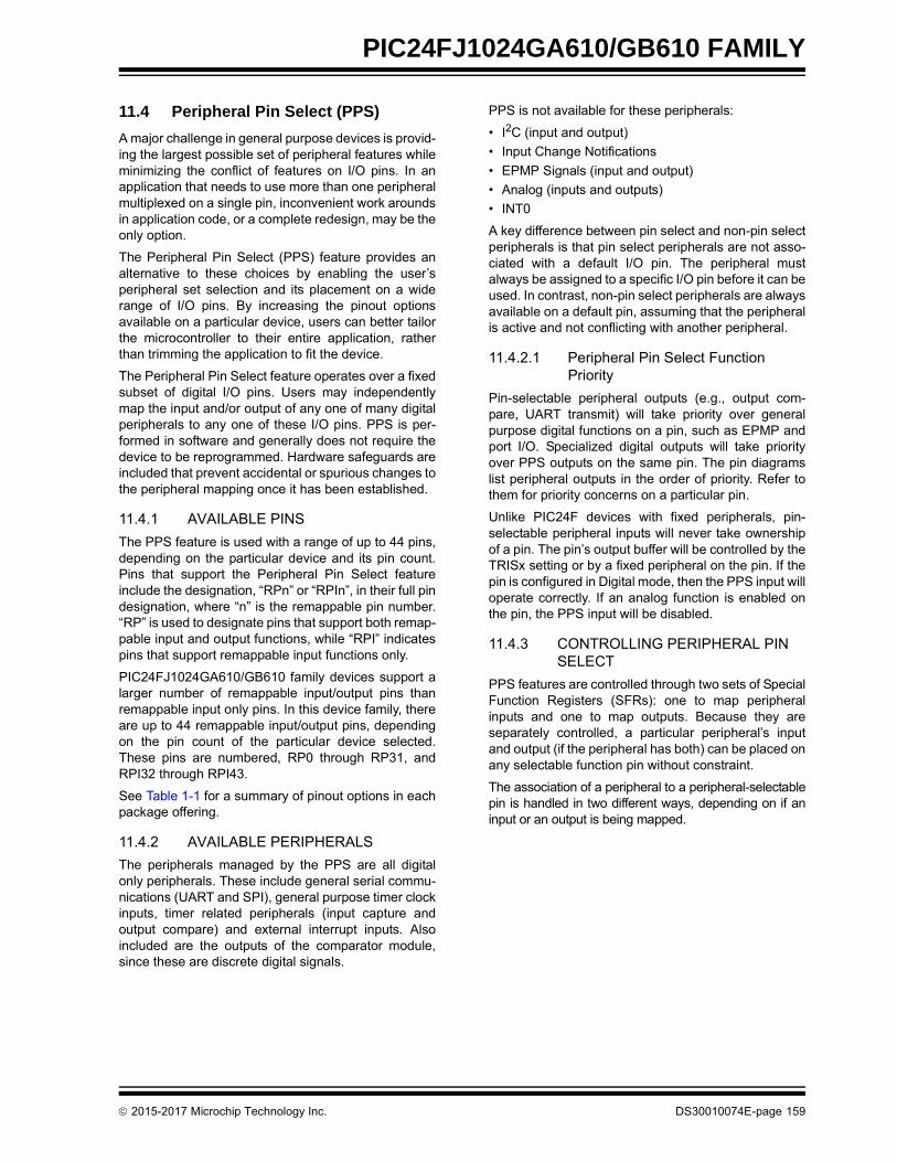
PIC24FJ1024GA610/GB610 FAMILY
11.4 Peripheral Pin Select (PPS)
A major challenge in general purpose devices is provid-ing the largest possible set of peripheral features whileminimizing the conflict of features on I/O pins. In anapplication that needs to use more than one peripheralmultiplexed on a single pin, inconvenient work aroundsin application code, or a complete redesign, may be theonly option.
The Peripheral Pin Select (PPS) feature provides analternative to these choices by enabling the user’speripheral set selection and its placement on a widerange of I/O pins. By increasing the pinout optionsavailable on a particular device, users can better tailorthe microcontroller to their entire application, ratherthan trimming the application to fit the device.
The Peripheral Pin Select feature operates over a fixedsubset of digital I/O pins. Users may independentlymap the input and/or output of any one of many digitalperipherals to any one of these I/O pins. PPS is per-formed in software and generally does not require thedevice to be reprogrammed. Hardware safeguards areincluded that prevent accidental or spurious changes tothe peripheral mapping once it has been established.
11.4.1 AVAILABLE PINS
The PPS feature is used with a range of up to 44 pins,depending on the particular device and its pin count.Pins that support the Peripheral Pin Select featureinclude the designation, “RPn” or “RPIn”, in their full pindesignation, where “n” is the remappable pin number.“RP” is used to designate pins that support both remap-pable input and output functions, while “RPI” indicatespins that support remappable input functions only.
PIC24FJ1024GA610/GB610 family devices support alarger number of remappable input/output pins thanremappable input only pins. In this device family, thereare up to 44 remappable input/output pins, dependingon the pin count of the particular device selected.These pins are numbered, RP0 through RP31, andRPI32 through RPI43.
See Table 1-1 for a summary of pinout options in eachpackage offering.
11.4.2 AVAILABLE PERIPHERALS
The peripherals managed by the PPS are all digitalonly peripherals. These include general serial commu-nications (UART and SPI), general purpose timer clockinputs, timer related peripherals (input capture andoutput compare) and external interrupt inputs. Alsoincluded are the outputs of the comparator module,since these are discrete digital signals.
PPS is not available for these peripherals:
• I2C (input and output)
• Input Change Notifications
• EPMP Signals (input and output)
• Analog (inputs and outputs)
• INT0
A key difference between pin select and non-pin selectperipherals is that pin select peripherals are not asso-ciated with a default I/O pin. The peripheral mustalways be assigned to a specific I/O pin before it can beused. In contrast, non-pin select peripherals are alwaysavailable on a default pin, assuming that the peripheralis active and not conflicting with another peripheral.
11.4.2.1 Peripheral Pin Select Function Priority
Pin-selectable peripheral outputs (e.g., output com-pare, UART transmit) will take priority over generalpurpose digital functions on a pin, such as EPMP andport I/O. Specialized digital outputs will take priorityover PPS outputs on the same pin. The pin diagramslist peripheral outputs in the order of priority. Refer tothem for priority concerns on a particular pin.
Unlike PIC24F devices with fixed peripherals, pin-selectable peripheral inputs will never take ownershipof a pin. The pin’s output buffer will be controlled by theTRISx setting or by a fixed peripheral on the pin. If thepin is configured in Digital mode, then the PPS input willoperate correctly. If an analog function is enabled onthe pin, the PPS input will be disabled.
11.4.3 CONTROLLING PERIPHERAL PIN SELECT
PPS features are controlled through two sets of SpecialFunction Registers (SFRs): one to map peripheralinputs and one to map outputs. Because they areseparately controlled, a particular peripheral’s inputand output (if the peripheral has both) can be placed onany selectable function pin without constraint.
The association of a peripheral to a peripheral-selectablepin is handled in two different ways, depending on if aninput or an output is being mapped.
2015-2017 Microchip Technology Inc. DS30010074E-page 159
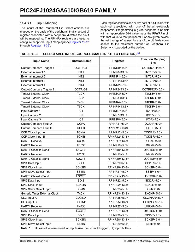
PIC24FJ1024GA610/GB610 FAMILY
11.4.3.1 Input Mapping
The inputs of the Peripheral Pin Select options aremapped on the basis of the peripheral; that is, a controlregister associated with a peripheral dictates the pin itwill be mapped to. The RPINRx registers are used toconfigure peripheral input mapping (see Register 11-12through Register 11-35).
Each register contains one or two sets of 6-bit fields, witheach set associated with one of the pin-selectableperipherals. Programming a given peripheral’s bit fieldwith an appropriate 6-bit value maps the RPn/RPIn pinwith that value to that peripheral. For any given device,the valid range of values for any of the bit fields corre-sponds to the maximum number of Peripheral PinSelections supported by the device.
TABLE 11-3: SELECTABLE INPUT SOURCES (MAPS INPUT TO FUNCTION)(1)
Input Name Function Name RegisterFunction Mapping
Bits
Output Compare Trigger 1 OCTRIG1 RPINR0<5:0> OCTRIG1R<5:0>
External Interrupt 1 INT1 RPINR0<13:8> INT1R<5:0>
External Interrupt 2 INT2 RPINR1<5:0> INT2R<5:0>
External Interrupt 3 INT3 RPINR1<13:8> INT3R<5:0>
External Interrupt 4 INT4 RPINR2<5:0> INT4R<5:0>
Output Compare Trigger 2 OCTRIG2 RPINR2<13:8> OCTRIG2R<5:0>
Timer2 External Clock T2CK RPINR3<5:0> T2CKR<5:0>
Timer3 External Clock T3CK RPINR3<13:8> T3CKR<5:0>
Timer4 External Clock T4CK RPINR4<5:0> T4CKR<5:0>
Timer5 External Clock T5CK RPINR4<13:8> T5CKR<5:0>
Input Capture 1 IC1 RPINR7<5:0> IC1R<5:0>
Input Capture 2 IC2 RPINR7<13:8> IC2R<5:0>
Input Capture 3 IC3 RPINR8<5:0> IC3R<5:0>
Output Compare Fault A OCFA RPINR11<5:0> OCFAR<5:0>
Output Compare Fault B OCFB RPINR11<13:8> OCFBR<5:0>
CCP Clock Input A TCKIA RPINR12<5:0> TCKIAR<5:0>
CCP Clock Input B TCKIB RPINR12<13:8> TCKIBR<5:0>
UART3 Receive U3RX RPINR17<13:8> U3RXR<5:0>
UART1 Receive U1RX RPINR18<5:0> U1RXR<5:0>
UART1 Clear-to-Send U1CTS RPINR18<13:8> U1CTSR<5:0>
UART2 Receive U2RX RPINR19<5:0> U2RXR<5:0>
UART2 Clear-to-Send U2CTS RPINR19<13:8> U2CTSR<5:0>
SPI1 Data Input SDI1 RPINR20<5:0> SDI1R<5:0>
SPI1 Clock Input SCK1IN RPINR20<13:8> SCK1R<5:0>
SPI1 Slave Select Input SS1IN RPINR21<5:0> SS1R<5:0>
UART3 Clear-to-Send U3CTS RPINR21<13:8> U3CTSR<5:0>
SPI2 Data Input SDI2 RPINR22<5:0> SDI2R<5:0>
SPI2 Clock Input SCK2IN RPINR22<13:8> SCK2R<5:0>
SPI2 Slave Select Input SS2IN RPINR23<5:0> SS2R<5:0>
Generic Timer External Clock TxCK RPINR23<13:8> TXCKR<5:0>
CLC Input A CLCINA RPINR25<5:0> CLCINAR<5:0>
CLC Input B CLCINB RPINR25<13:8> CLCINBR<5:0>
UART4 Receive U4RX RPINR27<5:0> U4RXR<5:0>
UART4 Clear-to-Send U4CTS RPINR27<13:8> U4CTSR<5:0>
SPI3 Data Input SDI3 RPINR28<5:0> SDI3R<5:0>
SPI3 Clock Input SCK3IN RPINR28<13:8> SCK3R<5:0>
SPI3 Slave Select Input SS3IN RPINR29<5:0> SS3R<5:0>
Note 1: Unless otherwise noted, all inputs use the Schmitt Trigger (ST) input buffers.
DS30010074E-page 160 2015-2017 Microchip Technology Inc.

PIC24FJ1024GA610/GB610 FAMILY
11.4.3.2 Output Mapping
In contrast to inputs, the outputs of the Peripheral PinSelect options are mapped on the basis of the pin. Inthis case, a control register associated with a particularpin dictates the peripheral output to be mapped. TheRPORx registers are used to control output mapping.Each register contains two 6-bit fields, with each fieldbeing associated with one RPn pin (see Register 11-36through Register 11-51). The value of the bit field
corresponds to one of the peripherals and thatperipheral’s output is mapped to the pin (seeTable 11-4).
Because of the mapping technique, the list of peripheralsfor output mapping also includes a null value of ‘000000’.This permits any given pin to remain disconnected fromthe output of any of the pin-selectable peripherals.
TABLE 11-4: SELECTABLE OUTPUT SOURCES (MAPS FUNCTION TO OUTPUT)
Output Function Number Function Output Name
0 None (Pin Disabled)
1 C1OUT Comparator 1 Output
2 C2OUT Comparator 2 Output
3 U1TX UART1 Transmit
4 U1RTS UART1 Request-to-Send
5 U2TX UART2 Transmit
6 U2RTS UART2 Request-to-Send
7 SDO1 SPI1 Data Output
8 SCK1OUT SPI1 Clock Output
9 SS1OUT SPI1 Slave Select Output
10 SDO2 SPI2 Data Output
11 SCK2OUT SPI2 Clock Output
12 SS2OUT SPI2 Slave Select Output
13 OC1 Output Compare 1
14 OC2 Output Compare 2
15 OC3 Output Compare 3
16 OCM4 CCP4 Output Compare
17 OCM5 CCP5 Output Compare
18 OCM6 CCP6 Output Compare
19 U3TX UART3 Transmit
20 U3RTS UART3 Request-to-Send
21 U4TX UART4 Transmit
22 U4RTS UART4 Request-to-Send
23 SDO3 SPI3 Data Output
24 SCK3OUT SPI3 Clock Output
25 SS3OUT SPI3 Slave Select Output
26 C3OUT Comparator 3 Output
27 OCM7 CCP7 Output Compare
28 REFO Reference Clock Output
29 CLC1OUT CLC1 Output
30 CLC2OUT CLC2 Output
31 RTCC RTCC Output
2015-2017 Microchip Technology Inc. DS30010074E-page 161

PIC24FJ1024GA610/GB610 FAMILY
11.4.3.3 Mapping Limitations
The control schema of the Peripheral Pin Select isextremely flexible. Other than systematic blocks thatprevent signal contention, caused by two physical pinsbeing configured as the same functional input or twofunctional outputs configured as the same pin, thereare no hardware enforced lockouts. The flexibilityextends to the point of allowing a single input to drivemultiple peripherals or a single functional output todrive multiple output pins.
11.4.3.4 Mapping Exceptions for PIC24FJ1024GA610/GB610 Family Devices
Although the PPS registers theoretically allow forinputs to be remapped to up to 64 pins, or for outputsto be remapped from 32 pins, not all of these areimplemented in all devices. For 100-pin or 121-pinvariants of the PIC24FJ1024GA610/GB610 familydevices, 32 remappable input/output pins are availableand 12 remappable input pins are available. For 64-pinvariants, 29 input/outputs and 1 input are available.The differences in available remappable pins aresummarized in Table 11-5.
When developing applications that use remappablepins, users should also keep these things in mind:
• For the RPINRx registers, bit combinations corre-sponding to an unimplemented pin for a particular device are treated as invalid; the corresponding module will not have an input mapped to it.
• For RPORx registers, the bit fields corresponding to an unimplemented pin will also be unimplemented; writing to these fields will have no effect.
11.4.4 CONTROLLING CONFIGURATION CHANGES
Because peripheral remapping can be changed duringrun time, some restrictions on peripheral remappingare needed to prevent accidental configurationchanges. PIC24F devices include three features toprevent alterations to the peripheral map:
• Control register lock sequence
• Continuous state monitoring
• Configuration bit remapping lock
11.4.4.1 Control Register Lock
Under normal operation, writes to the RPINRx andRPORx registers are not allowed. Attempted writes willappear to execute normally, but the contents of theregisters will remain unchanged. To change these reg-isters, they must be unlocked in hardware. The registerlock is controlled by the IOLOCK bit (OSCCON<6>).Setting IOLOCK prevents writes to the controlregisters; clearing IOLOCK allows writes.
To set or clear IOLOCK, a specific command sequencemust be executed:
1. Write 46h to OSCCON<7:0>.
2. Write 57h to OSCCON<7:0>.
3. Clear (or set) IOLOCK as a single operation.
Unlike the similar sequence with the oscillator’s LOCKbit, IOLOCK remains in one state until changed. Thisallows all of the Peripheral Pin Selects to be configuredwith a single unlock sequence, followed by an updateto all control registers, then locked with a second locksequence.
11.4.4.2 Continuous State Monitoring
In addition to being protected from direct writes, the con-tents of the RPINRx and RPORx registers are constantlymonitored in hardware by shadow registers. If an unex-pected change in any of the registers occurs (such as celldisturbances caused by ESD or other external events), aConfiguration Mismatch Reset will be triggered.
11.4.4.3 Configuration Bit Pin Select Lock
As an additional level of safety, the device can beconfigured to prevent more than one write session tothe RPINRx and RPORx registers. The IOL1WAY(FOSC<5>) Configuration bit blocks the IOLOCK bitfrom being cleared after it has been set once. IfIOLOCK remains set, the register unlock procedure willnot execute and the Peripheral Pin Select Control reg-isters cannot be written to. The only way to clear the bitand re-enable peripheral remapping is to perform adevice Reset.
In the default (unprogrammed) state, IOL1WAY is set,restricting users to one write session. ProgrammingIOL1WAY allows users unlimited access (with theproper use of the unlock sequence) to the PeripheralPin Select registers.
TABLE 11-5: REMAPPABLE PIN EXCEPTIONS FOR PIC24FJ1024GA610/GB610 FAMILY DEVICES
DeviceRPn Pins (I/O) RPIn Pins
Total Unimplemented Total Unimplemented
PIC24FJXXXGB606 28 RP5, RP15, RP30, RP31 1 All except RPI37
PIC24FJXXXGX61X 32 — 12 —
PIC24FJXXXGA606 29 RP5, RP15, RP31 1 All except RPI37
DS30010074E-page 162 2015-2017 Microchip Technology Inc.

PIC24FJ1024GA610/GB610 FAMILY
11.4.5 CONSIDERATIONS FOR PERIPHERAL PIN SELECTION
The ability to control Peripheral Pin Selection intro-duces several considerations into application designthat could be overlooked. This is particularly true forseveral common peripherals that are available only asremappable peripherals.
The main consideration is that the Peripheral PinSelects are not available on default pins in the device’sdefault (Reset) state. Since all RPINRx registers resetto ‘111111’ and all RPORx registers reset to ‘000000’,all Peripheral Pin Select inputs are tied to VSS, and allPeripheral Pin Select outputs are disconnected.
This situation requires the user to initialize the devicewith the proper peripheral configuration before anyother application code is executed. Since the IOLOCKbit resets in the unlocked state, it is not necessary toexecute the unlock sequence after the device hascome out of Reset. For application safety, however, it isbest to set IOLOCK and lock the configuration afterwriting to the control registers.
Because the unlock sequence is timing-critical, it mustbe executed as an assembly language routine in thesame manner as changes to the oscillator configura-tion. If the bulk of the application is written in ‘C’, oranother high-level language, the unlock sequenceshould be performed by writing in-line assembly.
Choosing the configuration requires the review of allPeripheral Pin Selects and their pin assignments,especially those that will not be used in the application.In all cases, unused pin-selectable peripherals shouldbe disabled completely. Unused peripherals shouldhave their inputs assigned to an unused RPn/RPIn pinfunction. I/O pins with unused RPn functions should beconfigured with the null peripheral output.
The assignment of a peripheral to a particular pin doesnot automatically perform any other configuration of thepin’s I/O circuitry. In theory, this means adding a pin-selectable output to a pin may mean inadvertentlydriving an existing peripheral input when the output isdriven. Users must be familiar with the behavior ofother fixed peripherals that share a remappable pin andknow when to enable or disable them. To be safe, fixeddigital peripherals that share the same pin should bedisabled when not in use.
Along these lines, configuring a remappable pin for aspecific peripheral does not automatically turn thatfeature on. The peripheral must be specifically config-ured for operation and enabled as if it were tied to afixed pin. Where this happens in the application code(immediately following a device Reset and peripheralconfiguration or inside the main application routine)depends on the peripheral and its use in theapplication.
A final consideration is that Peripheral Pin Select func-tions neither override analog inputs nor reconfigurepins with analog functions for digital I/O. If a pin isconfigured as an analog input on a device Reset, itmust be explicitly reconfigured as a digital I/O whenused with a Peripheral Pin Select.
Example 11-4 shows a configuration for bidirectionalcommunication with flow control using UART1. Thefollowing input and output functions are used:
• Input Functions: U1RX, U1CTS
• Output Functions: U1TX, U1RTS
EXAMPLE 11-4: CONFIGURING UART1 INPUT AND OUTPUT FUNCTIONS
// Unlock Registersasm volatile ("MOV #OSCCON, w1 \n"
"MOV #0x46, w2 \n" "MOV #0x57, w3 \n" "MOV.b w2, [w1] \n" "MOV.b w3, [w1] \n" "BCLR OSCCON, #6") ;
// or use XC16 built-in macro:// __builtin_write_OSCCONL(OSCCON & 0xbf);
// Configure Input Functions (Table 11-3)// Assign U1RX To Pin RP0RPINR18bits.U1RXR = 0;
// Assign U1CTS To Pin RP1RPINR18bits.U1CTSR = 1;
// Configure Output Functions (Table 11-4)// Assign U1TX To Pin RP2RPOR1bits.RP2R = 3;
// Assign U1RTS To Pin RP3RPOR1bits.RP3R = 4;
// Lock Registersasm volatile ("MOV #OSCCON, w1 \n"
"MOV #0x46, w2 \n""MOV #0x57, w3 \n""MOV.b w2, [w1] \n""MOV.b w3, [w1] \n""BSET OSCCON, #6") ;
// or use XC16 built-in macro:// __builtin_write_OSCCONL(OSCCON | 0x40);
2015-2017 Microchip Technology Inc. DS30010074E-page 163
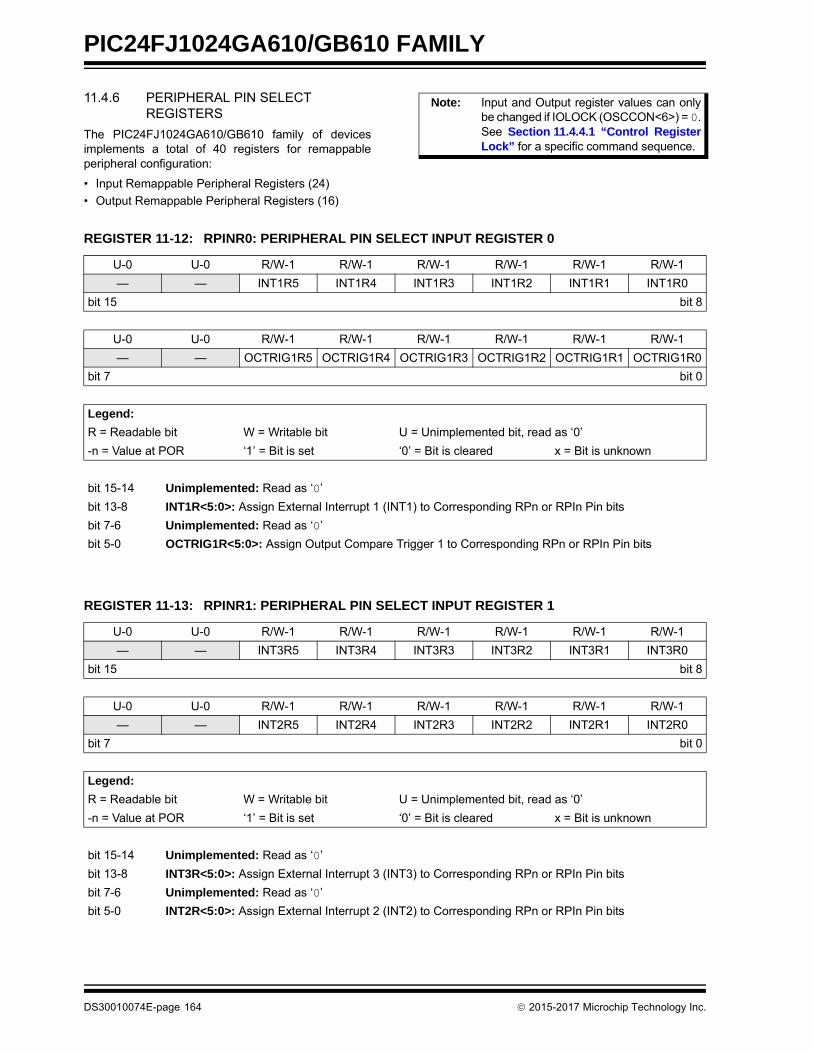
PIC24FJ1024GA610/GB610 FAMILY
11.4.6 PERIPHERAL PIN SELECT REGISTERS
The PIC24FJ1024GA610/GB610 family of devicesimplements a total of 40 registers for remappableperipheral configuration:
• Input Remappable Peripheral Registers (24)
• Output Remappable Peripheral Registers (16)
Note: Input and Output register values can onlybe changed if IOLOCK (OSCCON<6>) = 0.See Section 11.4.4.1 “Control RegisterLock” for a specific command sequence.
REGISTER 11-12: RPINR0: PERIPHERAL PIN SELECT INPUT REGISTER 0
U-0 U-0 R/W-1 R/W-1 R/W-1 R/W-1 R/W-1 R/W-1
— — INT1R5 INT1R4 INT1R3 INT1R2 INT1R1 INT1R0
bit 15 bit 8
U-0 U-0 R/W-1 R/W-1 R/W-1 R/W-1 R/W-1 R/W-1
— — OCTRIG1R5 OCTRIG1R4 OCTRIG1R3 OCTRIG1R2 OCTRIG1R1 OCTRIG1R0
bit 7 bit 0
Legend:
R = Readable bit W = Writable bit U = Unimplemented bit, read as ‘0’
-n = Value at POR ‘1’ = Bit is set ‘0’ = Bit is cleared x = Bit is unknown
bit 15-14 Unimplemented: Read as ‘0’
bit 13-8 INT1R<5:0>: Assign External Interrupt 1 (INT1) to Corresponding RPn or RPIn Pin bits
bit 7-6 Unimplemented: Read as ‘0’
bit 5-0 OCTRIG1R<5:0>: Assign Output Compare Trigger 1 to Corresponding RPn or RPIn Pin bits
REGISTER 11-13: RPINR1: PERIPHERAL PIN SELECT INPUT REGISTER 1
U-0 U-0 R/W-1 R/W-1 R/W-1 R/W-1 R/W-1 R/W-1
— — INT3R5 INT3R4 INT3R3 INT3R2 INT3R1 INT3R0
bit 15 bit 8
U-0 U-0 R/W-1 R/W-1 R/W-1 R/W-1 R/W-1 R/W-1
— — INT2R5 INT2R4 INT2R3 INT2R2 INT2R1 INT2R0
bit 7 bit 0
Legend:
R = Readable bit W = Writable bit U = Unimplemented bit, read as ‘0’
-n = Value at POR ‘1’ = Bit is set ‘0’ = Bit is cleared x = Bit is unknown
bit 15-14 Unimplemented: Read as ‘0’
bit 13-8 INT3R<5:0>: Assign External Interrupt 3 (INT3) to Corresponding RPn or RPIn Pin bits
bit 7-6 Unimplemented: Read as ‘0’
bit 5-0 INT2R<5:0>: Assign External Interrupt 2 (INT2) to Corresponding RPn or RPIn Pin bits
DS30010074E-page 164 2015-2017 Microchip Technology Inc.

PIC24FJ1024GA610/GB610 FAMILY
REGISTER 11-14: RPINR2: PERIPHERAL PIN SELECT INPUT REGISTER 2
U-0 U-0 R/W-1 R/W-1 R/W-1 R/W-1 R/W-1 R/W-1
— — OCTRIG2R5 OCTRIG2R4 OCTRIG2R3 OCTRIG2R2 OCTRIG2R1 OCTRIG2R0
bit 15 bit 8
U-0 U-0 R/W-1 R/W-1 R/W-1 R/W-1 R/W-1 R/W-1
— — INT4R5 INT4R4 INT4R3 INT4R2 INT4R1 INT4R0
bit 7 bit 0
Legend:
R = Readable bit W = Writable bit U = Unimplemented bit, read as ‘0’
-n = Value at POR ‘1’ = Bit is set ‘0’ = Bit is cleared x = Bit is unknown
bit 15-14 Unimplemented: Read as ‘0’
bit 13-8 OCTRIG2R<5:0>: Assign Output Compare Trigger 2 to Corresponding RPn or RPIn Pin bits
bit 7-6 Unimplemented: Read as ‘0’
bit 5-0 INT4R<5:0>: Assign External Interrupt 4 (INT4) to Corresponding RPn or RPIn Pin bits
REGISTER 11-15: RPINR3: PERIPHERAL PIN SELECT INPUT REGISTER 3
U-0 U-0 R/W-1 R/W-1 R/W-1 R/W-1 R/W-1 R/W-1
— — T3CKR5 T3CKR4 T3CKR3 T3CKR2 T3CKR1 T3CKR0
bit 15 bit 8
U-0 U-0 R/W-1 R/W-1 R/W-1 R/W-1 R/W-1 R/W-1
— — T2CKR5 T2CKR4 T2CKR3 T2CKR2 T2CKR1 T2CKR0
bit 7 bit 0
Legend:
R = Readable bit W = Writable bit U = Unimplemented bit, read as ‘0’
-n = Value at POR ‘1’ = Bit is set ‘0’ = Bit is cleared x = Bit is unknown
bit 15-14 Unimplemented: Read as ‘0’
bit 13-8 T3CKR<5:0>: Assign Timer3 Clock to Corresponding RPn or RPIn Pin bits
bit 7-6 Unimplemented: Read as ‘0’
bit 5-0 T2CKR<5:0>: Assign Timer2 Clock to Corresponding RPn or RPIn Pin bits
2015-2017 Microchip Technology Inc. DS30010074E-page 165
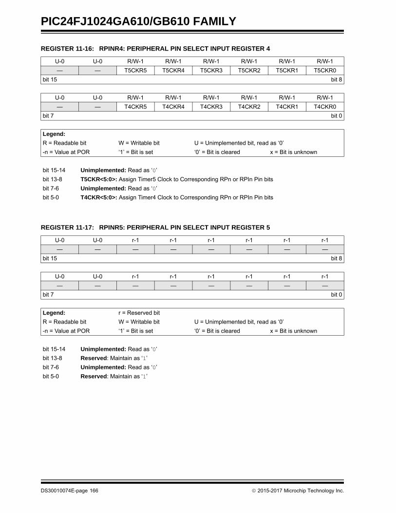
PIC24FJ1024GA610/GB610 FAMILY
REGISTER 11-16: RPINR4: PERIPHERAL PIN SELECT INPUT REGISTER 4
U-0 U-0 R/W-1 R/W-1 R/W-1 R/W-1 R/W-1 R/W-1
— — T5CKR5 T5CKR4 T5CKR3 T5CKR2 T5CKR1 T5CKR0
bit 15 bit 8
U-0 U-0 R/W-1 R/W-1 R/W-1 R/W-1 R/W-1 R/W-1
— — T4CKR5 T4CKR4 T4CKR3 T4CKR2 T4CKR1 T4CKR0
bit 7 bit 0
Legend:
R = Readable bit W = Writable bit U = Unimplemented bit, read as ‘0’
-n = Value at POR ‘1’ = Bit is set ‘0’ = Bit is cleared x = Bit is unknown
bit 15-14 Unimplemented: Read as ‘0’
bit 13-8 T5CKR<5:0>: Assign Timer5 Clock to Corresponding RPn or RPIn Pin bits
bit 7-6 Unimplemented: Read as ‘0’
bit 5-0 T4CKR<5:0>: Assign Timer4 Clock to Corresponding RPn or RPIn Pin bits
REGISTER 11-17: RPINR5: PERIPHERAL PIN SELECT INPUT REGISTER 5
U-0 U-0 r-1 r-1 r-1 r-1 r-1 r-1
— — — — — — — —
bit 15 bit 8
U-0 U-0 r-1 r-1 r-1 r-1 r-1 r-1
— — — — — — — —
bit 7 bit 0
Legend: r = Reserved bit
R = Readable bit W = Writable bit U = Unimplemented bit, read as ‘0’
-n = Value at POR ‘1’ = Bit is set ‘0’ = Bit is cleared x = Bit is unknown
bit 15-14 Unimplemented: Read as ‘0’
bit 13-8 Reserved: Maintain as ‘1’
bit 7-6 Unimplemented: Read as ‘0’
bit 5-0 Reserved: Maintain as ‘1’
DS30010074E-page 166 2015-2017 Microchip Technology Inc.

PIC24FJ1024GA610/GB610 FAMILY
REGISTER 11-18: RPINR6: PERIPHERAL PIN SELECT INPUT REGISTER 6
U-0 U-0 r-1 r-1 r-1 r-1 r-1 r-1
— — — — — — — —
bit 15 bit 8
U-0 U-0 r-1 r-1 r-1 r-1 r-1 r-1
— — — — — — — —
bit 7 bit 0
Legend: r = Reserved bit
R = Readable bit W = Writable bit U = Unimplemented bit, read as ‘0’
-n = Value at POR ‘1’ = Bit is set ‘0’ = Bit is cleared x = Bit is unknown
bit 15-14 Unimplemented: Read as ‘0’
bit 13-8 Reserved: Maintain as ‘1’
bit 7-6 Unimplemented: Read as ‘0’
bit 5-0 Reserved: Maintain as ‘1’
REGISTER 11-19: RPINR7: PERIPHERAL PIN SELECT INPUT REGISTER 7
U-0 U-0 R/W-1 R/W-1 R/W-1 R/W-1 R/W-1 R/W-1
— — IC2R5 IC2R4 IC2R3 IC2R2 IC2R1 IC2R0
bit 15 bit 8
U-0 U-0 R/W-1 R/W-1 R/W-1 R/W-1 R/W-1 R/W-1
— — IC1R5 IC1R4 IC1R3 IC1R2 IC1R1 IC1R0
bit 7 bit 0
Legend:
R = Readable bit W = Writable bit U = Unimplemented bit, read as ‘0’
-n = Value at POR ‘1’ = Bit is set ‘0’ = Bit is cleared x = Bit is unknown
bit 15-14 Unimplemented: Read as ‘0’
bit 13-8 IC2R<5:0>: Assign Input Capture 2 (IC2) to Corresponding RPn or RPIn Pin bits
bit 7-6 Unimplemented: Read as ‘0’
bit 5-0 IC1R<5:0>: Assign Input Capture 1 (IC1) to Corresponding RPn or RPIn Pin bits
2015-2017 Microchip Technology Inc. DS30010074E-page 167
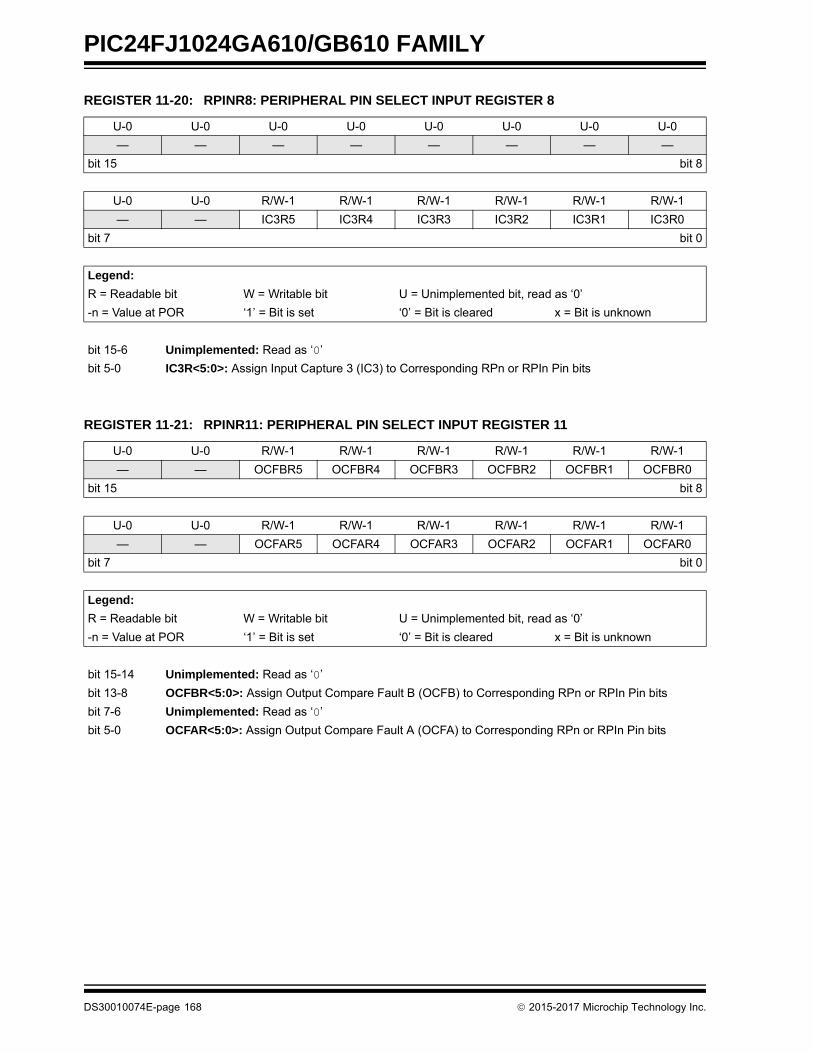
PIC24FJ1024GA610/GB610 FAMILY
REGISTER 11-20: RPINR8: PERIPHERAL PIN SELECT INPUT REGISTER 8
U-0 U-0 U-0 U-0 U-0 U-0 U-0 U-0
— — — — — — — —
bit 15 bit 8
U-0 U-0 R/W-1 R/W-1 R/W-1 R/W-1 R/W-1 R/W-1
— — IC3R5 IC3R4 IC3R3 IC3R2 IC3R1 IC3R0
bit 7 bit 0
Legend:
R = Readable bit W = Writable bit U = Unimplemented bit, read as ‘0’
-n = Value at POR ‘1’ = Bit is set ‘0’ = Bit is cleared x = Bit is unknown
bit 15-6 Unimplemented: Read as ‘0’
bit 5-0 IC3R<5:0>: Assign Input Capture 3 (IC3) to Corresponding RPn or RPIn Pin bits
REGISTER 11-21: RPINR11: PERIPHERAL PIN SELECT INPUT REGISTER 11
U-0 U-0 R/W-1 R/W-1 R/W-1 R/W-1 R/W-1 R/W-1
— — OCFBR5 OCFBR4 OCFBR3 OCFBR2 OCFBR1 OCFBR0
bit 15 bit 8
U-0 U-0 R/W-1 R/W-1 R/W-1 R/W-1 R/W-1 R/W-1
— — OCFAR5 OCFAR4 OCFAR3 OCFAR2 OCFAR1 OCFAR0
bit 7 bit 0
Legend:
R = Readable bit W = Writable bit U = Unimplemented bit, read as ‘0’
-n = Value at POR ‘1’ = Bit is set ‘0’ = Bit is cleared x = Bit is unknown
bit 15-14 Unimplemented: Read as ‘0’
bit 13-8 OCFBR<5:0>: Assign Output Compare Fault B (OCFB) to Corresponding RPn or RPIn Pin bits
bit 7-6 Unimplemented: Read as ‘0’
bit 5-0 OCFAR<5:0>: Assign Output Compare Fault A (OCFA) to Corresponding RPn or RPIn Pin bits
DS30010074E-page 168 2015-2017 Microchip Technology Inc.
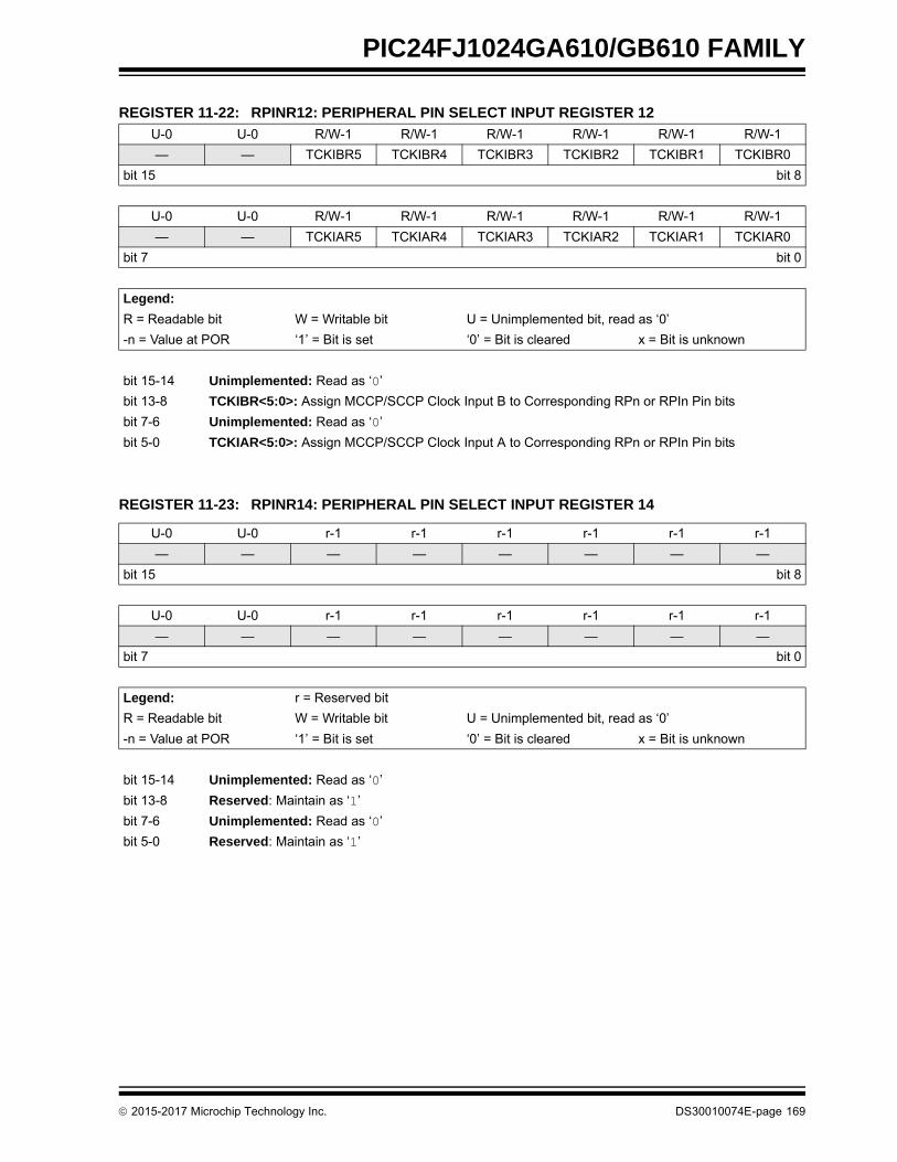
PIC24FJ1024GA610/GB610 FAMILY
REGISTER 11-22: RPINR12: PERIPHERAL PIN SELECT INPUT REGISTER 12
U-0 U-0 R/W-1 R/W-1 R/W-1 R/W-1 R/W-1 R/W-1
— — TCKIBR5 TCKIBR4 TCKIBR3 TCKIBR2 TCKIBR1 TCKIBR0
bit 15 bit 8
U-0 U-0 R/W-1 R/W-1 R/W-1 R/W-1 R/W-1 R/W-1
— — TCKIAR5 TCKIAR4 TCKIAR3 TCKIAR2 TCKIAR1 TCKIAR0
bit 7 bit 0
Legend:
R = Readable bit W = Writable bit U = Unimplemented bit, read as ‘0’
-n = Value at POR ‘1’ = Bit is set ‘0’ = Bit is cleared x = Bit is unknown
bit 15-14 Unimplemented: Read as ‘0’
bit 13-8 TCKIBR<5:0>: Assign MCCP/SCCP Clock Input B to Corresponding RPn or RPIn Pin bits
bit 7-6 Unimplemented: Read as ‘0’
bit 5-0 TCKIAR<5:0>: Assign MCCP/SCCP Clock Input A to Corresponding RPn or RPIn Pin bits
REGISTER 11-23: RPINR14: PERIPHERAL PIN SELECT INPUT REGISTER 14
U-0 U-0 r-1 r-1 r-1 r-1 r-1 r-1
— — — — — — — —
bit 15 bit 8
U-0 U-0 r-1 r-1 r-1 r-1 r-1 r-1
— — — — — — — —
bit 7 bit 0
Legend: r = Reserved bit
R = Readable bit W = Writable bit U = Unimplemented bit, read as ‘0’
-n = Value at POR ‘1’ = Bit is set ‘0’ = Bit is cleared x = Bit is unknown
bit 15-14 Unimplemented: Read as ‘0’
bit 13-8 Reserved: Maintain as ‘1’
bit 7-6 Unimplemented: Read as ‘0’
bit 5-0 Reserved: Maintain as ‘1’
2015-2017 Microchip Technology Inc. DS30010074E-page 169

PIC24FJ1024GA610/GB610 FAMILY
REGISTER 11-24: RPINR15: PERIPHERAL PIN SELECT INPUT REGISTER 15
U-0 U-0 U-0 U-0 U-0 U-0 U-0 U-0
— — — — — — — —
bit 15 bit 8
U-0 U-0 r-1 r-1 r-1 r-1 r-1 r-1
— — — — — — — —
bit 7 bit 0
Legend: r = Reserved bit
R = Readable bit W = Writable bit U = Unimplemented bit, read as ‘0’
-n = Value at POR ‘1’ = Bit is set ‘0’ = Bit is cleared x = Bit is unknown
bit 15-6 Unimplemented: Read as ‘0’
bit 5-0 Reserved: Maintain as ‘1’
REGISTER 11-25: RPINR17: PERIPHERAL PIN SELECT INPUT REGISTER 17
U-0 U-0 R/W-1 R/W-1 R/W-1 R/W-1 R/W-1 R/W-1
— — U3RXR5 U3RXR4 U3RXR3 U3RXR2 U3RXR1 U3RXR0
bit 15 bit 8
U-0 U-0 U-0 U-0 U-0 U-0 U-0 U-0
— — — — — — — —
bit 7 bit 0
Legend:
R = Readable bit W = Writable bit U = Unimplemented bit, read as ‘0’
-n = Value at POR ‘1’ = Bit is set ‘0’ = Bit is cleared x = Bit is unknown
bit 15-14 Unimplemented: Read as ‘0’
bit 13-8 U3RXR<5:0>: Assign UART3 Receive (U3RX) to Corresponding RPn or RPIn Pin bits
bit 7-0 Unimplemented: Read as ‘0’
DS30010074E-page 170 2015-2017 Microchip Technology Inc.

PIC24FJ1024GA610/GB610 FAMILY
REGISTER 11-26: RPINR18: PERIPHERAL PIN SELECT INPUT REGISTER 18
U-0 U-0 R/W-1 R/W-1 R/W-1 R/W-1 R/W-1 R/W-1
— — U1CTSR5 U1CTSR4 U1CTSR3 U1CTSR2 U1CTSR1 U1CTSR0
bit 15 bit 8
U-0 U-0 R/W-1 R/W-1 R/W-1 R/W-1 R/W-1 R/W-1
— — U1RXR5 U1RXR4 U1RXR3 U1RXR2 U1RXR1 U1RXR0
bit 7 bit 0
Legend:
R = Readable bit W = Writable bit U = Unimplemented bit, read as ‘0’
-n = Value at POR ‘1’ = Bit is set ‘0’ = Bit is cleared x = Bit is unknown
bit 15-14 Unimplemented: Read as ‘0’
bit 13-8 U1CTSR<5:0>: Assign UART1 Clear-to-Send (U1CTS) to Corresponding RPn or RPIn Pin bits
bit 7-6 Unimplemented: Read as ‘0’
bit 5-0 U1RXR<5:0>: Assign UART1 Receive (U1RX) to Corresponding RPn or RPIn Pin bits
REGISTER 11-27: RPINR19: PERIPHERAL PIN SELECT INPUT REGISTER 19
U-0 U-0 R/W-1 R/W-1 R/W-1 R/W-1 R/W-1 R/W-1
— — U2CTSR5 U2CTSR4 U2CTSR3 U2CTSR2 U2CTSR1 U2CTSR0
bit 15 bit 8
U-0 U-0 R/W-1 R/W-1 R/W-1 R/W-1 R/W-1 R/W-1
— — U2RXR5 U2RXR4 U2RXR3 U2RXR2 U2RXR1 U2RXR0
bit 7 bit 0
Legend:
R = Readable bit W = Writable bit U = Unimplemented bit, read as ‘0’
-n = Value at POR ‘1’ = Bit is set ‘0’ = Bit is cleared x = Bit is unknown
bit 15-14 Unimplemented: Read as ‘0’
bit 13-8 U2CTSR<5:0>: Assign UART2 Clear-to-Send (U2CTS) to Corresponding RPn or RPIn Pin bits
bit 7-6 Unimplemented: Read as ‘0’
bit 5-0 U2RXR<5:0>: Assign UART2 Receive (U2RX) to Corresponding RPn or RPIn Pin bits
2015-2017 Microchip Technology Inc. DS30010074E-page 171

PIC24FJ1024GA610/GB610 FAMILY
REGISTER 11-28: RPINR20: PERIPHERAL PIN SELECT INPUT REGISTER 20
U-0 U-0 R/W-1 R/W-1 R/W-1 R/W-1 R/W-1 R/W-1
— — SCK1R5 SCK1R4 SCK1R3 SCK1R2 SCK1R1 SCK1R0
bit 15 bit 8
U-0 U-0 R/W-1 R/W-1 R/W-1 R/W-1 R/W-1 R/W-1
— — SDI1R5 SDI1R4 SDI1R3 SDI1R2 SDI1R1 SDI1R0
bit 7 bit 0
Legend:
R = Readable bit W = Writable bit U = Unimplemented bit, read as ‘0’
-n = Value at POR ‘1’ = Bit is set ‘0’ = Bit is cleared x = Bit is unknown
bit 15-14 Unimplemented: Read as ‘0’
bit 13-8 SCK1R<5:0>: Assign SPI1 Clock Input (SCK1IN) to Corresponding RPn or RPIn Pin bits
bit 7-6 Unimplemented: Read as ‘0’
bit 5-0 SDI1R<5:0>: Assign SPI1 Data Input (SDI1) to Corresponding RPn or RPIn Pin bits
REGISTER 11-29: RPINR21: PERIPHERAL PIN SELECT INPUT REGISTER 21
U-0 U-0 R/W-1 R/W-1 R/W-1 R/W-1 R/W-1 R/W-1
— — U3CTSR5 U3CTSR4 U3CTSR3 U3CTSR2 U3CTSR1 U3CTSR0
bit 15 bit 8
U-0 U-0 R/W-1 R/W-1 R/W-1 R/W-1 R/W-1 R/W-1
— — SS1R5 SS1R4 SS1R3 SS1R2 SS1R1 SS1R0
bit 7 bit 0
Legend:
R = Readable bit W = Writable bit U = Unimplemented bit, read as ‘0’
-n = Value at POR ‘1’ = Bit is set ‘0’ = Bit is cleared x = Bit is unknown
bit 15-14 Unimplemented: Read as ‘0’
bit 13-8 U3CTSR<5:0>: Assign UART3 Clear-to-Send (U3CTS) to Corresponding RPn or RPIn Pin bits
bit 7-6 Unimplemented: Read as ‘0’
bit 5-0 SS1R<5:0>: Assign SPI1 Slave Select Input (SS1IN) to Corresponding RPn or RPIn Pin bits
DS30010074E-page 172 2015-2017 Microchip Technology Inc.
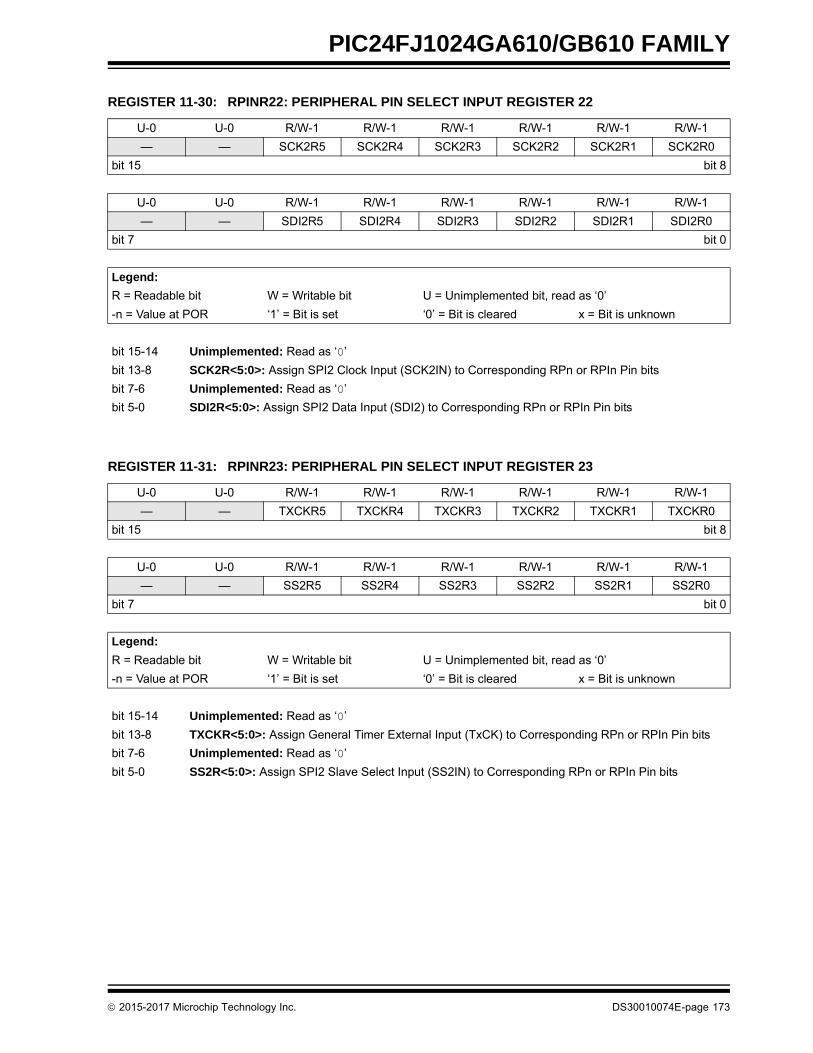
PIC24FJ1024GA610/GB610 FAMILY
REGISTER 11-30: RPINR22: PERIPHERAL PIN SELECT INPUT REGISTER 22
U-0 U-0 R/W-1 R/W-1 R/W-1 R/W-1 R/W-1 R/W-1
— — SCK2R5 SCK2R4 SCK2R3 SCK2R2 SCK2R1 SCK2R0
bit 15 bit 8
U-0 U-0 R/W-1 R/W-1 R/W-1 R/W-1 R/W-1 R/W-1
— — SDI2R5 SDI2R4 SDI2R3 SDI2R2 SDI2R1 SDI2R0
bit 7 bit 0
Legend:
R = Readable bit W = Writable bit U = Unimplemented bit, read as ‘0’
-n = Value at POR ‘1’ = Bit is set ‘0’ = Bit is cleared x = Bit is unknown
bit 15-14 Unimplemented: Read as ‘0’
bit 13-8 SCK2R<5:0>: Assign SPI2 Clock Input (SCK2IN) to Corresponding RPn or RPIn Pin bits
bit 7-6 Unimplemented: Read as ‘0’
bit 5-0 SDI2R<5:0>: Assign SPI2 Data Input (SDI2) to Corresponding RPn or RPIn Pin bits
REGISTER 11-31: RPINR23: PERIPHERAL PIN SELECT INPUT REGISTER 23
U-0 U-0 R/W-1 R/W-1 R/W-1 R/W-1 R/W-1 R/W-1
— — TXCKR5 TXCKR4 TXCKR3 TXCKR2 TXCKR1 TXCKR0
bit 15 bit 8
U-0 U-0 R/W-1 R/W-1 R/W-1 R/W-1 R/W-1 R/W-1
— — SS2R5 SS2R4 SS2R3 SS2R2 SS2R1 SS2R0
bit 7 bit 0
Legend:
R = Readable bit W = Writable bit U = Unimplemented bit, read as ‘0’
-n = Value at POR ‘1’ = Bit is set ‘0’ = Bit is cleared x = Bit is unknown
bit 15-14 Unimplemented: Read as ‘0’
bit 13-8 TXCKR<5:0>: Assign General Timer External Input (TxCK) to Corresponding RPn or RPIn Pin bits
bit 7-6 Unimplemented: Read as ‘0’
bit 5-0 SS2R<5:0>: Assign SPI2 Slave Select Input (SS2IN) to Corresponding RPn or RPIn Pin bits
2015-2017 Microchip Technology Inc. DS30010074E-page 173

PIC24FJ1024GA610/GB610 FAMILY
REGISTER 11-32: RPINR25: PERIPHERAL PIN SELECT INPUT REGISTER 25
U-0 U-0 R/W-1 R/W-1 R/W-1 R/W-1 R/W-1 R/W-1
— — CLCINBR5 CLCINBR4 CLCINBR3 CLCINBR2 CLCINBR1 CLCINBR0
bit 15 bit 8
U-0 U-0 R/W-1 R/W-1 R/W-1 R/W-1 R/W-1 R/W-1
— — CLCINAR5 CLCINAR4 CLCINAR3 CLCINAR2 CLCINAR1 CLCINAR0
bit 7 bit 0
Legend:
R = Readable bit W = Writable bit U = Unimplemented bit, read as ‘0’
-n = Value at POR ‘1’ = Bit is set ‘0’ = Bit is cleared x = Bit is unknown
bit 15-14 Unimplemented: Read as ‘0’
bit 13-8 CLCINBR<5:0>: Assign CLC Input B to Corresponding RPn or RPIn Pin bits
bit 7-6 Unimplemented: Read as ‘0’
bit 5-0 CLCINAR<5:0>: Assign CLC Input A to Corresponding RPn or RPIn Pin bits
REGISTER 11-33: RPINR27: PERIPHERAL PIN SELECT INPUT REGISTER 27
U-0 U-0 R/W-1 R/W-1 R/W-1 R/W-1 R/W-1 R/W-1
— — U4CTSR5 U4CTSR4 U4CTSR3 U4CTSR2 U4CTSR1 U4CTSR0
bit 15 bit 8
U-0 U-0 R/W-1 R/W-1 R/W-1 R/W-1 R/W-1 R/W-1
— — U4RXR5 U4RXR4 U4RXR3 U4RXR2 U4RXR1 U4RXR0
bit 7 bit 0
Legend:
R = Readable bit W = Writable bit U = Unimplemented bit, read as ‘0’
-n = Value at POR ‘1’ = Bit is set ‘0’ = Bit is cleared x = Bit is unknown
bit 15-14 Unimplemented: Read as ‘0’
bit 13-8 U4CTSR<5:0>: Assign UART4 Clear-to-Send Input (U4CTS) to Corresponding RPn or RPIn Pin bits
bit 7-6 Unimplemented: Read as ‘0’
bit 5-0 U4RXR<5:0>: Assign UART4 Receive Input (U4RX) to Corresponding RPn or RPIn Pin bits
DS30010074E-page 174 2015-2017 Microchip Technology Inc.
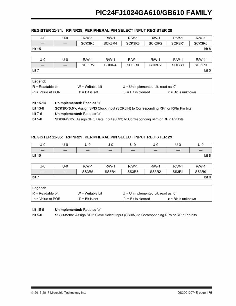
PIC24FJ1024GA610/GB610 FAMILY
REGISTER 11-34: RPINR28: PERIPHERAL PIN SELECT INPUT REGISTER 28
U-0 U-0 R/W-1 R/W-1 R/W-1 R/W-1 R/W-1 R/W-1
— — SCK3R5 SCK3R4 SCK3R3 SCK3R2 SCK3R1 SCK3R0
bit 15 bit 8
U-0 U-0 R/W-1 R/W-1 R/W-1 R/W-1 R/W-1 R/W-1
— — SDI3R5 SDI3R4 SDI3R3 SDI3R2 SDI3R1 SDI3R0
bit 7 bit 0
Legend:
R = Readable bit W = Writable bit U = Unimplemented bit, read as ‘0’
-n = Value at POR ‘1’ = Bit is set ‘0’ = Bit is cleared x = Bit is unknown
bit 15-14 Unimplemented: Read as ‘0’
bit 13-8 SCK3R<5:0>: Assign SPI3 Clock Input (SCK3IN) to Corresponding RPn or RPIn Pin bits
bit 7-6 Unimplemented: Read as ‘0’
bit 5-0 SDI3R<5:0>: Assign SPI3 Data Input (SDI3) to Corresponding RPn or RPIn Pin bits
REGISTER 11-35: RPINR29: PERIPHERAL PIN SELECT INPUT REGISTER 29
U-0 U-0 U-0 U-0 U-0 U-0 U-0 U-0
— — — — — — — —
bit 15 bit 8
U-0 U-0 R/W-1 R/W-1 R/W-1 R/W-1 R/W-1 R/W-1
— — SS3R5 SS3R4 SS3R3 SS3R2 SS3R1 SS3R0
bit 7 bit 0
Legend:
R = Readable bit W = Writable bit U = Unimplemented bit, read as ‘0’
-n = Value at POR ‘1’ = Bit is set ‘0’ = Bit is cleared x = Bit is unknown
bit 15-6 Unimplemented: Read as ‘0’
bit 5-0 SS3R<5:0>: Assign SPI3 Slave Select Input (SS3IN) to Corresponding RPn or RPIn Pin bits
2015-2017 Microchip Technology Inc. DS30010074E-page 175

PIC24FJ1024GA610/GB610 FAMILY
REGISTER 11-36: RPOR0: PERIPHERAL PIN SELECT OUTPUT REGISTER 0
U-0 U-0 R/W-0 R/W-0 R/W-0 R/W-0 R/W-0 R/W-0
— — RP1R5 RP1R4 RP1R3 RP1R2 RP1R1 RP1R0
bit 15 bit 8
U-0 U-0 R/W-0 R/W-0 R/W-0 R/W-0 R/W-0 R/W-0
— — RP0R5 RP0R4 RP0R3 RP0R2 RP0R1 RP0R0
bit 7 bit 0
Legend:
R = Readable bit W = Writable bit U = Unimplemented bit, read as ‘0’
-n = Value at POR ‘1’ = Bit is set ‘0’ = Bit is cleared x = Bit is unknown
bit 15-14 Unimplemented: Read as ‘0’
bit 13-8 RP1R<5:0>: RP1 Output Pin Mapping bits
Peripheral Output Number n is assigned to pin, RP1 (see Table 11-4 for peripheral function numbers).
bit 7-6 Unimplemented: Read as ‘0’
bit 5-0 RP0R<5:0>: RP0 Output Pin Mapping bits
Peripheral Output Number n is assigned to pin, RP0 (see Table 11-4 for peripheral function numbers).
REGISTER 11-37: RPOR1: PERIPHERAL PIN SELECT OUTPUT REGISTER 1
U-0 U-0 R/W-0 R/W-0 R/W-0 R/W-0 R/W-0 R/W-0
— — RP3R5 RP3R4 RP3R3 RP3R2 RP3R1 RP3R0
bit 15 bit 8
U-0 U-0 R/W-0 R/W-0 R/W-0 R/W-0 R/W-0 R/W-0
— — RP2R5 RP2R4 RP2R3 RP2R2 RP2R1 RP2R0
bit 7 bit 0
Legend:
R = Readable bit W = Writable bit U = Unimplemented bit, read as ‘0’
-n = Value at POR ‘1’ = Bit is set ‘0’ = Bit is cleared x = Bit is unknown
bit 15-14 Unimplemented: Read as ‘0’
bit 13-8 RP3R<5:0>: RP3 Output Pin Mapping bits
Peripheral Output Number n is assigned to pin, RP3 (see Table 11-4 for peripheral function numbers).
bit 7-6 Unimplemented: Read as ‘0’
bit 5-0 RP2R<5:0>: RP2 Output Pin Mapping bits
Peripheral Output Number n is assigned to pin, RP2 (see Table 11-4 for peripheral function numbers).
DS30010074E-page 176 2015-2017 Microchip Technology Inc.

PIC24FJ1024GA610/GB610 FAMILY
REGISTER 11-38: RPOR2: PERIPHERAL PIN SELECT OUTPUT REGISTER 2
U-0 U-0 R/W-0 R/W-0 R/W-0 R/W-0 R/W-0 R/W-0
— — RP5R5(1) RP5R4(1) RP5R3(1) RP5R2(1) RP5R1(1) RP5R0(1)
bit 15 bit 8
U-0 U-0 R/W-0 R/W-0 R/W-0 R/W-0 R/W-0 R/W-0
— — RP4R5 RP4R4 RP4R3 RP4R2 RP4R1 RP4R0
bit 7 bit 0
Legend:
R = Readable bit W = Writable bit U = Unimplemented bit, read as ‘0’
-n = Value at POR ‘1’ = Bit is set ‘0’ = Bit is cleared x = Bit is unknown
bit 15-14 Unimplemented: Read as ‘0’
bit 13-8 RP5R<5:0>: RP5 Output Pin Mapping bits(1)
Peripheral Output Number n is assigned to pin, RP5 (see Table 11-4 for peripheral function numbers).
bit 7-6 Unimplemented: Read as ‘0’
bit 5-0 RP4R<5:0>: RP4 Output Pin Mapping bits
Peripheral Output Number n is assigned to pin, RP4 (see Table 11-4 for peripheral function numbers).
Note 1: This pin is not available on 64-pin devices.
REGISTER 11-39: RPOR3: PERIPHERAL PIN SELECT OUTPUT REGISTER 3
U-0 U-0 R/W-0 R/W-0 R/W-0 R/W-0 R/W-0 R/W-0
— — RP7R5 RP7R4 RP7R3 RP7R2 RP7R1 RP7R0
bit 15 bit 8
U-0 U-0 R/W-0 R/W-0 R/W-0 R/W-0 R/W-0 R/W-0
— — RP6R5 RP6R4 RP6R3 RP6R2 RP6R1 RP6R0
bit 7 bit 0
Legend:
R = Readable bit W = Writable bit U = Unimplemented bit, read as ‘0’
-n = Value at POR ‘1’ = Bit is set ‘0’ = Bit is cleared x = Bit is unknown
bit 15-14 Unimplemented: Read as ‘0’
bit 13-8 RP7R<5:0>: RP7 Output Pin Mapping bits
Peripheral Output Number n is assigned to pin, RP7 (see Table 11-4 for peripheral function numbers).
bit 7-6 Unimplemented: Read as ‘0’
bit 5-0 RP6R<5:0>: RP6 Output Pin Mapping bits
Peripheral Output Number n is assigned to pin, RP6 (see Table 11-4 for peripheral function numbers).
2015-2017 Microchip Technology Inc. DS30010074E-page 177

PIC24FJ1024GA610/GB610 FAMILY
REGISTER 11-40: RPOR4: PERIPHERAL PIN SELECT OUTPUT REGISTER 4
U-0 U-0 R/W-0 R/W-0 R/W-0 R/W-0 R/W-0 R/W-0
— — RP9R5 RP9R4 RP9R3 RP9R2 RP9R1 RP9R0
bit 15 bit 8
U-0 U-0 R/W-0 R/W-0 R/W-0 R/W-0 R/W-0 R/W-0
— — RP8R5 RP8R4 RP8R3 RP8R2 RP8R1 RP8R0
bit 7 bit 0
Legend:
R = Readable bit W = Writable bit U = Unimplemented bit, read as ‘0’
-n = Value at POR ‘1’ = Bit is set ‘0’ = Bit is cleared x = Bit is unknown
bit 15-14 Unimplemented: Read as ‘0’
bit 13-8 RP9R<5:0>: RP9 Output Pin Mapping bits
Peripheral Output Number n is assigned to pin, RP9 (see Table 11-4 for peripheral function numbers).
bit 7-6 Unimplemented: Read as ‘0’
bit 5-0 RP8R<5:0>: RP8 Output Pin Mapping bits
Peripheral Output Number n is assigned to pin, RP8 (see Table 11-4 for peripheral function numbers).
REGISTER 11-41: RPOR5: PERIPHERAL PIN SELECT OUTPUT REGISTER 5
U-0 U-0 R/W-0 R/W-0 R/W-0 R/W-0 R/W-0 R/W-0
— — RP11R5 RP11R4 RP11R3 RP11R2 RP11R1 RP11R0
bit 15 bit 8
U-0 U-0 R/W-0 R/W-0 R/W-0 R/W-0 R/W-0 R/W-0
— — RP10R5 RP10R4 RP10R3 RP10R2 RP10R1 RP10R0
bit 7 bit 0
Legend:
R = Readable bit W = Writable bit U = Unimplemented bit, read as ‘0’
-n = Value at POR ‘1’ = Bit is set ‘0’ = Bit is cleared x = Bit is unknown
bit 15-14 Unimplemented: Read as ‘0’
bit 13-8 RP11R<5:0>: RP11 Output Pin Mapping bits
Peripheral Output Number n is assigned to pin, RP11 (see Table 11-4 for peripheral function numbers).
bit 7-6 Unimplemented: Read as ‘0’
bit 5-0 RP10R<5:0>: RP10 Output Pin Mapping bits
Peripheral Output Number n is assigned to pin, RP10 (see Table 11-4 for peripheral function numbers).
DS30010074E-page 178 2015-2017 Microchip Technology Inc.

PIC24FJ1024GA610/GB610 FAMILY
REGISTER 11-42: RPOR6: PERIPHERAL PIN SELECT OUTPUT REGISTER 6
U-0 U-0 R/W-0 R/W-0 R/W-0 R/W-0 R/W-0 R/W-0
— — RP13R5 RP13R4 RP13R3 RP13R2 RP13R1 RP13R0
bit 15 bit 8
U-0 U-0 R/W-0 R/W-0 R/W-0 R/W-0 R/W-0 R/W-0
— — RP12R5 RP12R4 RP12R3 RP12R2 RP12R1 RP12R0
bit 7 bit 0
Legend:
R = Readable bit W = Writable bit U = Unimplemented bit, read as ‘0’
-n = Value at POR ‘1’ = Bit is set ‘0’ = Bit is cleared x = Bit is unknown
bit 15-14 Unimplemented: Read as ‘0’
bit 13-8 RP13R<5:0>: RP13 Output Pin Mapping bits
Peripheral Output Number n is assigned to pin, RP13 (see Table 11-4 for peripheral function numbers).
bit 7-6 Unimplemented: Read as ‘0’
bit 5-0 RP12R<5:0>: RP12 Output Pin Mapping bits
Peripheral Output Number n is assigned to pin, RP12 (see Table 11-4 for peripheral function numbers).
REGISTER 11-43: RPOR7: PERIPHERAL PIN SELECT OUTPUT REGISTER 7
U-0 U-0 R/W-0 R/W-0 R/W-0 R/W-0 R/W-0 R/W-0
— — RP15R5(1) RP15R4(1) RP15R3(1) RP15R2(1) RP15R1(1) RP15R0(1)
bit 15 bit 8
U-0 U-0 R/W-0 R/W-0 R/W-0 R/W-0 R/W-0 R/W-0
— — RP14R5 RP14R4 RP14R3 RP14R2 RP14R1 RP14R0
bit 7 bit 0
Legend:
R = Readable bit W = Writable bit U = Unimplemented bit, read as ‘0’
-n = Value at POR ‘1’ = Bit is set ‘0’ = Bit is cleared x = Bit is unknown
bit 15-14 Unimplemented: Read as ‘0’
bit 13-8 RP15R<5:0>: RP15 Output Pin Mapping bits(1)
Peripheral Output Number n is assigned to pin, RP15 (see Table 11-4 for peripheral function numbers).
bit 7-6 Unimplemented: Read as ‘0’
bit 5-0 RP14R<5:0>: RP14 Output Pin Mapping bits
Peripheral Output Number n is assigned to pin, RP14 (see Table 11-4 for peripheral function numbers).
Note 1: This pin is not available on 64-pin devices.
2015-2017 Microchip Technology Inc. DS30010074E-page 179

PIC24FJ1024GA610/GB610 FAMILY
REGISTER 11-44: RPOR8: PERIPHERAL PIN SELECT OUTPUT REGISTER 8
U-0 U-0 R/W-0 R/W-0 R/W-0 R/W-0 R/W-0 R/W-0
— — RP17R5 RP17R4 RP17R3 RP17R2 RP17R1 RP17R0
bit 15 bit 8
U-0 U-0 R/W-0 R/W-0 R/W-0 R/W-0 R/W-0 R/W-0
— — RP16R5 RP16R4 RP16R3 RP16R2 RP16R1 RP16R0
bit 7 bit 0
Legend:
R = Readable bit W = Writable bit U = Unimplemented bit, read as ‘0’
-n = Value at POR ‘1’ = Bit is set ‘0’ = Bit is cleared x = Bit is unknown
bit 15-14 Unimplemented: Read as ‘0’
bit 13-8 RP17R<5:0>: RP17 Output Pin Mapping bits
Peripheral Output Number n is assigned to pin, RP17 (see Table 11-4 for peripheral function numbers).
bit 7-6 Unimplemented: Read as ‘0’
bit 5-0 RP16R<5:0>: RP16 Output Pin Mapping bits
Peripheral Output Number n is assigned to pin, RP16 (see Table 11-4 for peripheral function numbers).
REGISTER 11-45: RPOR9: PERIPHERAL PIN SELECT OUTPUT REGISTER 9
U-0 U-0 R/W-0 R/W-0 R/W-0 R/W-0 R/W-0 R/W-0
— — RP19R5 RP19R4 RP19R3 RP19R2 RP19R1 RP19R0
bit 15 bit 8
U-0 U-0 R/W-0 R/W-0 R/W-0 R/W-0 R/W-0 R/W-0
— — RP18R5 RP18R4 RP18R3 RP18R2 RP18R1 RP18R0
bit 7 bit 0
Legend:
R = Readable bit W = Writable bit U = Unimplemented bit, read as ‘0’
-n = Value at POR ‘1’ = Bit is set ‘0’ = Bit is cleared x = Bit is unknown
bit 15-14 Unimplemented: Read as ‘0’
bit 13-8 RP19R<5:0>: RP19 Output Pin Mapping bits
Peripheral Output Number n is assigned to pin, RP19 (see Table 11-4 for peripheral function numbers).
bit 7-6 Unimplemented: Read as ‘0’
bit 5-0 RP18R<5:0>: RP18 Output Pin Mapping bits
Peripheral Output Number n is assigned to pin, RP18 (see Table 11-4 for peripheral function numbers).
DS30010074E-page 180 2015-2017 Microchip Technology Inc.
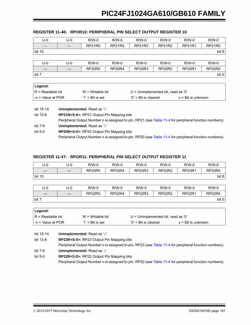
PIC24FJ1024GA610/GB610 FAMILY
REGISTER 11-46: RPOR10: PERIPHERAL PIN SELECT OUTPUT REGISTER 10
U-0 U-0 R/W-0 R/W-0 R/W-0 R/W-0 R/W-0 R/W-0
— — RP21R5 RP21R4 RP21R3 RP21R2 RP21R1 RP21R0
bit 15 bit 8
U-0 U-0 R/W-0 R/W-0 R/W-0 R/W-0 R/W-0 R/W-0
— — RP20R5 RP20R4 RP20R3 RP20R2 RP20R1 RP20R0
bit 7 bit 0
Legend:
R = Readable bit W = Writable bit U = Unimplemented bit, read as ‘0’
-n = Value at POR ‘1’ = Bit is set ‘0’ = Bit is cleared x = Bit is unknown
bit 15-14 Unimplemented: Read as ‘0’
bit 13-8 RP21R<5:0>: RP21 Output Pin Mapping bits
Peripheral Output Number n is assigned to pin, RP21 (see Table 11-4 for peripheral function numbers).
bit 7-6 Unimplemented: Read as ‘0’
bit 5-0 RP20R<5:0>: RP20 Output Pin Mapping bits
Peripheral Output Number n is assigned to pin, RP20 (see Table 11-4 for peripheral function numbers).
REGISTER 11-47: RPOR11: PERIPHERAL PIN SELECT OUTPUT REGISTER 11
U-0 U-0 R/W-0 R/W-0 R/W-0 R/W-0 R/W-0 R/W-0
— — RP23R5 RP23R4 RP23R3 RP23R2 RP23R1 RP23R0
bit 15 bit 8
U-0 U-0 R/W-0 R/W-0 R/W-0 R/W-0 R/W-0 R/W-0
— — RP22R5 RP22R4 RP22R3 RP22R2 RP22R1 RP22R0
bit 7 bit 0
Legend:
R = Readable bit W = Writable bit U = Unimplemented bit, read as ‘0’
-n = Value at POR ‘1’ = Bit is set ‘0’ = Bit is cleared x = Bit is unknown
bit 15-14 Unimplemented: Read as ‘0’
bit 13-8 RP23R<5:0>: RP23 Output Pin Mapping bits
Peripheral Output Number n is assigned to pin, RP23 (see Table 11-4 for peripheral function numbers).
bit 7-6 Unimplemented: Read as ‘0’
bit 5-0 RP22R<5:0>: RP22 Output Pin Mapping bits
Peripheral Output Number n is assigned to pin, RP22 (see Table 11-4 for peripheral function numbers).
2015-2017 Microchip Technology Inc. DS30010074E-page 181

PIC24FJ1024GA610/GB610 FAMILY
REGISTER 11-48: RPOR12: PERIPHERAL PIN SELECT OUTPUT REGISTER 12
U-0 U-0 R/W-0 R/W-0 R/W-0 R/W-0 R/W-0 R/W-0
— — RP25R5 RP25R4 RP25R3 RP25R2 RP25R1 RP25R0
bit 15 bit 8
U-0 U-0 R/W-0 R/W-0 R/W-0 R/W-0 R/W-0 R/W-0
— — RP24R5 RP24R4 RP24R3 RP24R2 RP24R1 RP24R0
bit 7 bit 0
Legend:
R = Readable bit W = Writable bit U = Unimplemented bit, read as ‘0’
-n = Value at POR ‘1’ = Bit is set ‘0’ = Bit is cleared x = Bit is unknown
bit 15-14 Unimplemented: Read as ‘0’
bit 13-8 RP25R<5:0>: RP25 Output Pin Mapping bits
Peripheral Output Number n is assigned to pin, RP25 (see Table 11-4 for peripheral function numbers).
bit 7-6 Unimplemented: Read as ‘0’
bit 5-0 RP24R<5:0>: RP24 Output Pin Mapping bits
Peripheral Output Number n is assigned to pin, RP24 (see Table 11-4 for peripheral function numbers).
REGISTER 11-49: RPOR13: PERIPHERAL PIN SELECT OUTPUT REGISTER 13
U-0 U-0 R/W-0 R/W-0 R/W-0 R/W-0 R/W-0 R/W-0
— — RP27R5 RP27R4 RP27R3 RP27R2 RP27R1 RP27R0
bit 15 bit 8
U-0 U-0 R/W-0 R/W-0 R/W-0 R/W-0 R/W-0 R/W-0
— — RP26R5 RP26R4 RP26R3 RP26R2 RP26R1 RP26R0
bit 7 bit 0
Legend:
R = Readable bit W = Writable bit U = Unimplemented bit, read as ‘0’
-n = Value at POR ‘1’ = Bit is set ‘0’ = Bit is cleared x = Bit is unknown
bit 15-14 Unimplemented: Read as ‘0’
bit 13-8 RP27R<5:0>: RP27 Output Pin Mapping bits
Peripheral Output Number n is assigned to pin, RP27 (see Table 11-4 for peripheral function numbers).
bit 7-6 Unimplemented: Read as ‘0’
bit 5-0 RP26R<5:0>: RP26 Output Pin Mapping bits
Peripheral Output Number n is assigned to pin, RP26 (see Table 11-4 for peripheral function numbers).
DS30010074E-page 182 2015-2017 Microchip Technology Inc.

PIC24FJ1024GA610/GB610 FAMILY
REGISTER 11-50: RPOR14: PERIPHERAL PIN SELECT OUTPUT REGISTER 14
U-0 U-0 R/W-0 R/W-0 R/W-0 R/W-0 R/W-0 R/W-0
— — RP29R5 RP29R4 RP29R3 RP29R2 RP29R1 RP29R0
bit 15 bit 8
U-0 U-0 R/W-0 R/W-0 R/W-0 R/W-0 R/W-0 R/W-0
— — RP28R5 RP28R4 RP28R3 RP28R2 RP28R1 RP28R0
bit 7 bit 0
Legend:
R = Readable bit W = Writable bit U = Unimplemented bit, read as ‘0’
-n = Value at POR ‘1’ = Bit is set ‘0’ = Bit is cleared x = Bit is unknown
bit 15-14 Unimplemented: Read as ‘0’
bit 13-8 RP29R<5:0>: RP29 Output Pin Mapping bits
Peripheral Output Number n is assigned to pin, RP29 (see Table 11-4 for peripheral function numbers).
bit 7-6 Unimplemented: Read as ‘0’
bit 5-0 RP28R<5:0>: RP28 Output Pin Mapping bits
Peripheral Output Number n is assigned to pin, RP28 (see Table 11-4 for peripheral function numbers).
REGISTER 11-51: RPOR15: PERIPHERAL PIN SELECT OUTPUT REGISTER 15
U-0 U-0 R/W-0 R/W-0 R/W-0 R/W-0 R/W-0 R/W-0
— — RP31R5(1) RP31R4(1) RP31R3(1) RP31R2(1) RP31R1(1) RP31R0(1)
bit 15 bit 8
U-0 U-0 R/W-0 R/W-0 R/W-0 R/W-0 R/W-0 R/W-0
— — RP30R5(2) RP30R4(2) RP30R3(2) RP30R2(2) RP30R1(2) RP30R0(2)
bit 7 bit 0
Legend:
R = Readable bit W = Writable bit U = Unimplemented bit, read as ‘0’
-n = Value at POR ‘1’ = Bit is set ‘0’ = Bit is cleared x = Bit is unknown
bit 15-14 Unimplemented: Read as ‘0’
bit 13-8 RP31R<5:0>: RP31 Output Pin Mapping bits(1)
Peripheral Output Number n is assigned to pin, RP31 (see Table 11-4 for peripheral function numbers).
bit 7-6 Unimplemented: Read as ‘0’
bit 5-0 RP30R<5:0>: RP30 Output Pin Mapping bits(2)
Peripheral Output Number n is assigned to pin, RP30 (see Table 11-4 for peripheral function numbers).
Note 1: These pins are not available in 64-pin devices.
2: These pins are not available on the PIC24FJXXXGB606.
2015-2017 Microchip Technology Inc. DS30010074E-page 183

PIC24FJ1024GA610/GB610 FAMILY
NOTES:
DS30010074E-page 184 2015-2017 Microchip Technology Inc.
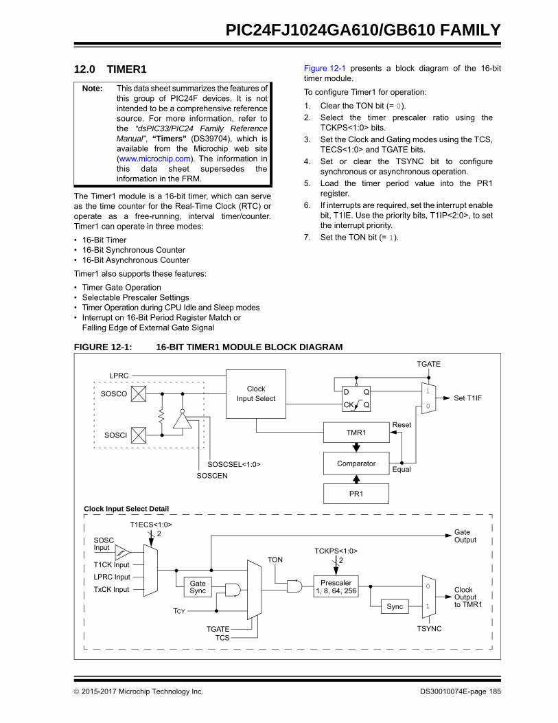
PIC24FJ1024GA610/GB610 FAMILY
12.0 TIMER1
The Timer1 module is a 16-bit timer, which can serveas the time counter for the Real-Time Clock (RTC) oroperate as a free-running, interval timer/counter.Timer1 can operate in three modes:
• 16-Bit Timer• 16-Bit Synchronous Counter• 16-Bit Asynchronous Counter
Timer1 also supports these features:
• Timer Gate Operation• Selectable Prescaler Settings• Timer Operation during CPU Idle and Sleep modes• Interrupt on 16-Bit Period Register Match or
Falling Edge of External Gate Signal
Figure 12-1 presents a block diagram of the 16-bittimer module.
To configure Timer1 for operation:
1. Clear the TON bit (= 0).
2. Select the timer prescaler ratio using theTCKPS<1:0> bits.
3. Set the Clock and Gating modes using the TCS,TECS<1:0> and TGATE bits.
4. Set or clear the TSYNC bit to configuresynchronous or asynchronous operation.
5. Load the timer period value into the PR1register.
6. If interrupts are required, set the interrupt enablebit, T1IE. Use the priority bits, T1IP<2:0>, to setthe interrupt priority.
7. Set the TON bit (= 1).
FIGURE 12-1: 16-BIT TIMER1 MODULE BLOCK DIAGRAM
Note: This data sheet summarizes the features ofthis group of PIC24F devices. It is notintended to be a comprehensive referencesource. For more information, refer tothe “dsPIC33/PIC24 Family ReferenceManual”, “Timers” (DS39704), which isavailable from the Microchip web site(www.microchip.com). The information inthis data sheet supersedes theinformation in the FRM.
TON
Sync
SOSCI
SOSCO
PR1
Set T1IF
EqualComparator
Reset
SOSCEN
1
0
TSYNC
Q
QD
CK
TCKPS<1:0>2
TGATE
TCY
1
0
TCSTGATE
SOSCInput
GateOutput
Clock Input Select Detail
LPRC Input
2T1ECS<1:0>
T1CK Input
SOSCSEL<1:0>
LPRC
ClockInput Select
Prescaler1, 8, 64, 256TxCK Input
TMR1
GateSync Clock
Outputto TMR1
2015-2017 Microchip Technology Inc. DS30010074E-page 185

PIC24FJ1024GA610/GB610 FAMILY
REGISTER 12-1: T1CON: TIMER1 CONTROL REGISTER(1)
R/W-0 U-0 R/W-0 U-0 U-0 U-0 R/W-0 R/W-0
TON — TSIDL — — — TECS1 TECS0
bit 15 bit 8
U-0 R/W-0 R/W-0 R/W-0 U-0 R/W-0 R/W-0 U-0
— TGATE TCKPS1 TCKPS0 — TSYNC TCS —
bit 7 bit 0
Legend:
R = Readable bit W = Writable bit U = Unimplemented bit, read as ‘0’
-n = Value at POR ‘1’ = Bit is set ‘0’ = Bit is cleared x = Bit is unknown
bit 15 TON: Timer1 On bit
1 = Starts 16-bit Timer10 = Stops 16-bit Timer1
bit 14 Unimplemented: Read as ‘0’
bit 13 TSIDL: Timer1 Stop in Idle Mode bit
1 = Discontinues module operation when device enters Idle mode0 = Continues module operation in Idle mode
bit 12-10 Unimplemented: Read as ‘0’
bit 9-8 TECS<1:0>: Timer1 Extended Clock Source Select bits (selected when TCS = 1)
11 = Generic timer (TxCK) external input10 = LPRC Oscillator01 = T1CK external clock input00 = SOSC
bit 7 Unimplemented: Read as ‘0’
bit 6 TGATE: Timer1 Gated Time Accumulation Enable bitWhen TCS = 1:This bit is ignored.
When TCS = 0: 1 = Gated time accumulation is enabled0 = Gated time accumulation is disabled
bit 5-4 TCKPS<1:0>: Timer1 Input Clock Prescale Select bits11 = 1:256 10 = 1:6401 = 1:8 00 = 1:1
bit 3 Unimplemented: Read as ‘0’
bit 2 TSYNC: Timer1 External Clock Input Synchronization Select bitWhen TCS = 1:1 = Synchronizes the external clock input0 = Does not synchronize the external clock input
When TCS = 0: This bit is ignored.
bit 1 TCS: Timer1 Clock Source Select bit1 = Extended clock is selected by the timer0 = Internal clock (FOSC/2)
bit 0 Unimplemented: Read as ‘0’
Note 1: Changing the value of T1CON while the timer is running (TON = 1) causes the timer prescale counter to reset and is not recommended.
DS30010074E-page 186 2015-2017 Microchip Technology Inc.

PIC24FJ1024GA610/GB610 FAMILY
13.0 TIMER2/3 AND TIMER4/5
The Timer2/3 and Timer4/5 modules are 32-bit timers,which can also be configured as four independent, 16-bittimers with selectable operating modes.
As 32-bit timers, Timer2/3 and Timer4/5 can eachoperate in three modes:
• Two Independent 16-Bit Timers with All 16-Bit Operating modes (except Asynchronous Counter mode)
• Single 32-Bit Timer
• Single 32-Bit Synchronous Counter
They also support these features:
• Timer Gate Operation
• Selectable Prescaler Settings
• Timer Operation during Idle and Sleep modes
• Interrupt on a 32-Bit Period Register Match
• A/D Event Trigger (only on Timer2/3 in 32-bit mode and Timer3 in 16-bit mode)
Individually, all four of the 16-bit timers can function assynchronous timers or counters. They also offer thefeatures listed above, except for the A/D Event Trigger.This Trigger is implemented only on Timer2/3 in 32-bitmode and Timer3 in 16-bit mode. The operating modesand enabled features are determined by setting theappropriate bit(s) in the T2CON, T3CON, T4CON andT5CON registers. T2CON and T4CON are shown ingeneric form in Register 13-1; T3CON and T5CON areshown in Register 13-2.
For 32-bit timer/counter operation, Timer2 and Timer4are the least significant word; Timer3 and Timer5 arethe most significant word of the 32-bit timers.
To configure Timer2/3 or Timer4/5 for 32-bit operation:
1. Set the T32 or T45 bit (T2CON<3> orT4CON<3> = 1).
2. Select the prescaler ratio for Timer2 or Timer4using the TCKPS<1:0> bits.
3. Set the Clock and Gating modes using the TCSand TGATE bits. If TCS is set to an externalclock, RPINRx (TyCK) must be configured toan available RPn/RPIn pin. For more informa-tion, see Section 11.4 “Peripheral Pin Select(PPS)”.
4. Load the timer period value. PR3 (or PR5) willcontain the most significant word (msw) of thevalue, while PR2 (or PR4) contains the leastsignificant word (lsw).
5. If interrupts are required, set the interrupt enablebit, T3IE or T5IE. Use the priority bits, T3IP<2:0>or T5IP<2:0>, to set the interrupt priority. Notethat while Timer2 or Timer4 controls the timer, theinterrupt appears as a Timer3 or Timer5 interrupt.
6. Set the TON bit (= 1).
The timer value, at any point, is stored in the registerpair, TMR<3:2> (or TMR<5:4>). TMR3 (TMR5) alwayscontains the most significant word of the count, whileTMR2 (TMR4) contains the least significant word.
To configure any of the timers for individual 16-bitoperation:
1. Clear the T32 bit corresponding to that timer(T2CON<3> for Timer2 and Timer3 orT4CON<3> for Timer4 and Timer5).
2. Select the timer prescaler ratio using theTCKPS<1:0> bits.
3. Set the Clock and Gating modes using the TCSand TGATE bits. See Section 11.4 “PeripheralPin Select (PPS)” for more information.
4. Load the timer period value into the PRx register.
5. If interrupts are required, set the interrupt enablebit, TxIE. Use the priority bits, TxIP<2:0>, to setthe interrupt priority.
6. Set the TON (TxCON<15> = 1) bit.
Note: This data sheet summarizes the features ofthis group of PIC24F devices. It is notintended to be a comprehensive referencesource. For more information, refer tothe “dsPIC33/PIC24 Family ReferenceManual”, “Timers” (DS39704), which isavailable from the Microchip web site(www.microchip.com). The information inthis data sheet supersedes theinformation in the FRM.
Note: For 32-bit operation, T3CON and T5CONcontrol bits are ignored. Only T2CON andT4CON control bits are used for setup andcontrol. Timer2 and Timer4 clock and gateinputs are utilized for the 32-bit timermodules, but an interrupt is generatedwith the Timer3 or Timer5 interrupt flags.
2015-2017 Microchip Technology Inc. DS30010074E-page 187

PIC24FJ1024GA610/GB610 FAMILY
FIGURE 13-1: TIMER2/3 AND TIMER4/5 (32-BIT) BLOCK DIAGRAM
TMR3 TMR2
Set T3IF (T5IF)
EqualComparator
PR3 PR2
Reset
LSBMSB
Note 1: The 32-Bit Timer Configuration bit, T32, must be set for 32-bit timer/counter operation. All control bits are respective to the T2CON and T4CON registers.
2: The timer clock input must be assigned to an available RPn/RPIn pin before use. See Section 11.4 “Peripheral Pin Select (PPS)” for more information.
3: The A/D Event Trigger is available only on Timer2/3 in 32-bit mode and Timer3 in 16-bit mode.
Data Bus<15:0>
Read TMR2 (TMR4)(1)
Write TMR2 (TMR4)(1)
16
16
16
Q
Q D
CK
TGATE
0
1
TCKPS<1:0>
2
A/D Event Trigger(3)
(PR5) (PR4)
(TMR5) (TMR4)
T2CK(T4CK) TCY
TCS(2)TGATE(2)
SOSC Input
LPRC Input
TECS<1:0>
TxCK
GateSync
Prescaler1, 8, 64, 256
Sync
TMR3HLD(TMR5HLD)
DS30010074E-page 188 2015-2017 Microchip Technology Inc.

PIC24FJ1024GA610/GB610 FAMILY
FIGURE 13-2: TIMER2 AND TIMER4 (16-BIT SYNCHRONOUS) BLOCK DIAGRAM
FIGURE 13-3: TIMER3 AND TIMER5 (16-BIT ASYNCHRONOUS) BLOCK DIAGRAM
TON
TCKPS<1:0>
Prescaler1, 8, 64, 256
2
T2CK
Set T2IF (T4IF)
Equal
Reset
Q
Q D
CK
TGATE
1
0
(T4CK)
Sync
Note 1: The timer clock input must be assigned to an available RPn/RPIn pin before use. See Section 11.4 “Peripheral Pin Select (PPS)” for more information.
TMR2 (TMR4)
TCY
TCS(1)TGATE(1)
SOSC Input
LPRC Input
TECS<1:0>
TxCK
GateSync
Comparator
PR2 (PR4)
TON
TCKPS<1:0>2
PR3 (PR5)
Set T3IF (T5IF)
EqualComparator
TMR3 (TMR5)Reset
Q
Q D
CK
TGATE
1
0
A/D Event Trigger(2)
Prescaler1, 8, 64, 256
Note 1: The timer clock input must be assigned to an available RPn/RPIn pin before use. See Section 11.4 “Peripheral Pin Select (PPS)” for more information.
2: The A/D Event Trigger is available only on Timer3.
T3CK(T5CK)
TCY
TCS(1)TGATE(1)
SOSC Input
LPRC Input
TECS<1:0>
TxCK
GateSync
2015-2017 Microchip Technology Inc. DS30010074E-page 189

PIC24FJ1024GA610/GB610 FAMILY
REGISTER 13-1: TxCON: TIMER2 AND TIMER4 CONTROL REGISTER(1)
R/W-0 U-0 R/W-0 U-0 U-0 U-0 R/W-0 R/W-0
TON — TSIDL — — — TECS1(2) TECS0(2)
bit 15 bit 8
U-0 R/W-0 R/W-0 R/W-0 R/W-0 U-0 R/W-0 U-0
— TGATE TCKPS1 TCKPS0 T32(3,4) — TCS(2) —
bit 7 bit 0
Legend:
R = Readable bit W = Writable bit U = Unimplemented bit, read as ‘0’
-n = Value at POR ‘1’ = Bit is set ‘0’ = Bit is cleared x = Bit is unknown
bit 15 TON: Timerx On bit
When TxCON<3> = 1:1 = Starts 32-bit Timerx/y0 = Stops 32-bit Timerx/y
When TxCON<3> = 0:1 = Starts 16-bit Timerx0 = Stops 16-bit Timerx
bit 14 Unimplemented: Read as ‘0’
bit 13 TSIDL: Timerx Stop in Idle Mode bit
1 = Discontinues module operation when device enters Idle mode0 = Continues module operation in Idle mode
bit 12-10 Unimplemented: Read as ‘0’
bit 9-8 TECS<1:0>: Timerx Extended Clock Source Select bits (selected when TCS = 1)(2)
When TCS = 1: 11 = Generic timer (TxCK) external input 10 = LPRC Oscillator01 = TyCK external clock input00 = SOSC
When TCS = 0: These bits are ignored; the timer is clocked from the internal system clock (FOSC/2).
bit 7 Unimplemented: Read as ‘0’
bit 6 TGATE: Timerx Gated Time Accumulation Enable bit
When TCS = 1: This bit is ignored.
When TCS = 0: 1 = Gated time accumulation is enabled0 = Gated time accumulation is disabled
bit 5-4 TCKPS<1:0>: Timerx Input Clock Prescale Select bits
11 = 1:256 10 = 1:6401 = 1:8 00 = 1:1
Note 1: Changing the value of TxCON while the timer is running (TON = 1) causes the timer prescale counter to reset and is not recommended.
2: If TCS = 1 and TECS<1:0> = x1, the selected external timer input (TxCK or TyCK) must be configured to an available RPn/RPIn pin. For more information, see Section 11.4 “Peripheral Pin Select (PPS)”.
3: In 32-bit mode, the T3CON or T5CON control bits do not affect 32-bit timer operation.
4: This bit is labeled T45 in the T4CON register.
DS30010074E-page 190 2015-2017 Microchip Technology Inc.

PIC24FJ1024GA610/GB610 FAMILY
bit 3 T32: 32-Bit Timer Mode Select bit(3,4)
1 = Timerx and Timery form a single 32-bit timer0 = Timerx and Timery act as two 16-bit timersIn 32-bit mode, T3CON control bits do not affect 32-bit timer operation.
bit 2 Unimplemented: Read as ‘0’
bit 1 TCS: Timerx Clock Source Select bit(2)
1 = Timer source is selected by TECS<1:0> 0 = Internal clock (FOSC/2)
bit 0 Unimplemented: Read as ‘0’
REGISTER 13-1: TxCON: TIMER2 AND TIMER4 CONTROL REGISTER(1) (CONTINUED)
Note 1: Changing the value of TxCON while the timer is running (TON = 1) causes the timer prescale counter to reset and is not recommended.
2: If TCS = 1 and TECS<1:0> = x1, the selected external timer input (TxCK or TyCK) must be configured to an available RPn/RPIn pin. For more information, see Section 11.4 “Peripheral Pin Select (PPS)”.
3: In 32-bit mode, the T3CON or T5CON control bits do not affect 32-bit timer operation.
4: This bit is labeled T45 in the T4CON register.
2015-2017 Microchip Technology Inc. DS30010074E-page 191

PIC24FJ1024GA610/GB610 FAMILY
REGISTER 13-2: TyCON: TIMER3 AND TIMER5 CONTROL REGISTER(1)
R/W-0 U-0 R/W-0 U-0 U-0 U-0 R/W-0 R/W-0
TON(2) — TSIDL(2) — — — TECS1(2,3) TECS0(2,3)
bit 15 bit 8
U-0 R/W-0 R/W-0 R/W-0 U-0 U-0 R/W-0 U-0
— TGATE(2) TCKPS1(2) TCKPS0(2) — — TCS(2,3) —
bit 7 bit 0
Legend:
R = Readable bit W = Writable bit U = Unimplemented bit, read as ‘0’
-n = Value at POR ‘1’ = Bit is set ‘0’ = Bit is cleared x = Bit is unknown
bit 15 TON: Timery On bit(2)
1 = Starts 16-bit Timery0 = Stops 16-bit Timery
bit 14 Unimplemented: Read as ‘0’
bit 13 TSIDL: Timery Stop in Idle Mode bit(2)
1 = Discontinues module operation when device enters Idle mode0 = Continues module operation in Idle mode
bit 12-10 Unimplemented: Read as ‘0’
bit 9-8 TECS<1:0>: Timery Extended Clock Source Select bits (selected when TCS = 1)(2,3)
11 = Generic timer (TxCK) external input10 = LPRC Oscillator01 = TyCK external clock input00 = SOSC
bit 7 Unimplemented: Read as ‘0’
bit 6 TGATE: Timery Gated Time Accumulation Enable bit(2)
When TCS = 1: This bit is ignored.
When TCS = 0: 1 = Gated time accumulation is enabled0 = Gated time accumulation is disabled
bit 5-4 TCKPS<1:0>: Timery Input Clock Prescale Select bits(2)
11 = 1:25610 = 1:6401 = 1:8 00 = 1:1
bit 3-2 Unimplemented: Read as ‘0’
bit 1 TCS: Timery Clock Source Select bit(2,3)
1 = External clock from pin, TyCK (on the rising edge) 0 = Internal clock (FOSC/2)
bit 0 Unimplemented: Read as ‘0’
Note 1: Changing the value of TyCON while the timer is running (TON = 1) causes the timer prescale counter to reset and is not recommended.
2: When 32-bit operation is enabled (T2CON<3> or T4CON<3> = 1), these bits have no effect on Timery operation; all timer functions are set through T2CON and T4CON.
3: If TCS = 1 and TECS<1:0> = x1, the selected external timer input (TyCK) must be configured to an available RPn/RPIn pin. For more information, see Section 11.4 “Peripheral Pin Select (PPS)”.
DS30010074E-page 192 2015-2017 Microchip Technology Inc.

PIC24FJ1024GA610/GB610 FAMILY
14.0 INPUT CAPTURE WITH DEDICATED TIMERS
Devices in the PIC24FJ1024GA610/GB610 familycontain six independent input capture modules. Eachof the modules offers a wide range of configuration andoperating options for capturing external pulse eventsand generating interrupts.
Key features of the input capture module include:
• Hardware-Configurable for 32-Bit Operation in all modes by Cascading Two Adjacent modules
• Synchronous and Trigger modes of Output Compare Operation with up to 31 User-Selectable Sync/Trigger Sources Available
• A 4-Level FIFO Buffer for Capturing and Holding Timer Values for Several Events
• Configurable Interrupt Generation• Up to 6 Clock Sources Available for each module,
Driving a Separate Internal 16-Bit Counter
The module is controlled through two registers: ICxCON1(Register 14-1) and ICxCON2 (Register 14-2). A generalblock diagram of the module is shown in Figure 14-1.
14.1 General Operating Modes
14.1.1 SYNCHRONOUS AND TRIGGER MODES
When the input capture module operates in a Free-Running mode, the internal 16-bit counter, ICxTMR,counts up continuously, wrapping around from FFFFhto 0000h on each overflow. Its period is synchronizedto the selected external clock source. When a captureevent occurs, the current 16-bit value of the internalcounter is written to the FIFO buffer.
In Synchronous mode, the module begins capturingevents on the ICx pin as soon as its selected clocksource is enabled. Whenever an event occurs on theselected Sync source, the internal counter is reset. InTrigger mode, the module waits for a Sync event fromanother internal module to occur before allowing theinternal counter to run.
Standard, free-running operation is selected by settingthe SYNCSEL<4:0> bits (ICxCON2<4:0>) to ‘00000’and clearing the ICTRIG bit (ICxCON2<7>). Synchro-nous and Trigger modes are selected any time theSYNCSELx bits are set to any value except ‘00000’.The ICTRIG bit selects either Synchronous or Triggermode; setting the bit selects Trigger mode operation. Inboth modes, the SYNCSELx bits determine the Sync/Trigger source.
When the SYNCSELx bits are set to ‘00000’ andICTRIG is set, the module operates in Software Triggermode. In this case, capture operations are started bymanually setting the TRIGSTAT bit (ICxCON2<6>).
FIGURE 14-1: INPUT CAPTURE x BLOCK DIAGRAM
Note: This data sheet summarizes the featuresof this group of PIC24F devices. It isnot intended to be a comprehensivereference source. For more information,refer to the “dsPIC33/PIC24 Family Refer-ence Manual”, ”Input Capture withDedicated Timer” (DS70000352), whichis available from the Microchip web site(www.microchip.com). The information inthis data sheet supersedes theinformation in the FRM.
Note 1: The ICx input must be assigned to an available RPn/RPIn pin before use. See Section 11.4 “Peripheral Pin Select (PPS)” for more information.
ICxBUF
4-Level FIFO Buffer
ICx Pin(1)
ICM<2:0>
Set ICxIFEdge Detect Logic
ICI1<:0>
ICOV, ICBNE System Bus
PrescalerCounter1:1/4/16
andClock Synchronizer
ClockSelect
ICx ClockSources
Sync and
ICTSEL<2:0>
SYNCSEL<4:0>Trigger
16
16
16
Increment
ResetSync andTriggerLogicTrigger Sources
ICxTMR
InterruptLogic
Event and
2015-2017 Microchip Technology Inc. DS30010074E-page 193

PIC24FJ1024GA610/GB610 FAMILY
14.1.2 CASCADED (32-BIT) MODE
By default, each module operates independently withits own 16-bit timer. To increase resolution, adjacenteven and odd modules can be configured to function asa single 32-bit module. (For example, Modules 1 and 2are paired, as are Modules 3 and 4, and so on.) Theodd numbered module (ICx) provides the Least Signif-icant 16 bits of the 32-bit register pairs and the evennumbered module (ICy) provides the Most Significant16 bits. Wrap-arounds of the ICx registers cause anincrement of their corresponding ICy registers.
Cascaded operation is configured in hardware bysetting the IC32 bits (ICxCON2<8>) for both modules.
14.2 Capture Operations
The input capture module can be configured to capturetimer values and generate interrupts on rising edges onICx or all transitions on ICx. Captures can be config-ured to occur on all rising edges or just some (every 4th
or 16th). Interrupts can be independently configured togenerate on each event or a subset of events.
To set up the module for capture operations:
1. Configure the ICx input for one of the availablePeripheral Pin Select pins.
2. If Synchronous mode is to be used, disable theSync source before proceeding.
3. Make sure that any previous data has beenremoved from the FIFO by reading ICxBUF untilthe ICBNE bit (ICxCON1<3>) is cleared.
4. Set the SYNCSELx bits (ICxCON2<4:0>) to thedesired Sync/Trigger source.
5. Set the ICTSELx bits (ICxCON1<12:10>) for thedesired clock source.
6. Set the ICIx bits (ICxCON1<6:5>) to the desiredinterrupt frequency.
7. Select Synchronous or Trigger mode operation:
a) Check that the SYNCSELx bits are not setto ‘00000’.
b) For Synchronous mode, clear the ICTRIGbit (ICxCON2<7>).
c) For Trigger mode, set ICTRIG and clear theTRIGSTAT bit (ICxCON2<6>).
8. Set the ICMx bits (ICxCON1<2:0>) to thedesired operational mode.
9. Enable the selected Sync/Trigger source.
For 32-bit cascaded operations, the setup procedure isslightly different:
1. Set the IC32 bits for both modules (ICyCON2<8>and ICxCON2<8>), enabling the even numberedmodule first. This ensures the modules will startfunctioning in unison.
2. Set the ICTSELx and SYNCSELx bits for bothmodules to select the same Sync/Trigger andtime base source. Set the even module first, thenthe odd module. Both modules must use thesame ICTSELx and SYNCSELx bits settings.
3. Clear the ICTRIG bit of the even module(ICyCON2<7>). This forces the module to run inSynchronous mode with the odd module,regardless of its Trigger setting.
4. Use the odd module’s ICIx bits (ICxCON1<6:5>)to set the desired interrupt frequency.
5. Use the ICTRIG bit of the odd module(ICxCON2<7>) to configure Trigger orSynchronous mode operation.
6. Use the ICMx bits of the odd module(ICxCON1<2:0>) to set the desired Capturemode.
The module is ready to capture events when the timebase and the Sync/Trigger source are enabled. Whenthe ICBNE bit (ICxCON1<3>) becomes set, at leastone capture value is available in the FIFO. Read inputcapture values from the FIFO until the ICBNE clearsto ‘0’.
For 32-bit operation, read both the ICxBUF andICyBUF for the full 32-bit timer value (ICxBUF for thelsw, ICyBUF for the msw). At least one capture value isavailable in the FIFO buffer when the odd module’sICBNE bit (ICxCON1<3>) becomes set. Continue toread the buffer registers until ICBNE is cleared(performed automatically by hardware).
Note: For Synchronous mode operation, enablethe Sync source as the last step. Bothinput capture modules are held in Resetuntil the Sync source is enabled.
DS30010074E-page 194 2015-2017 Microchip Technology Inc.

PIC24FJ1024GA610/GB610 FAMILY
REGISTER 14-1: ICxCON1: INPUT CAPTURE x CONTROL REGISTER 1
U-0 U-0 R/W-0 R/W-0 R/W-0 R/W-0 U-0 U-0
— — ICSIDL ICTSEL2 ICTSEL1 ICTSEL0 — —
bit 15 bit 8
U-0 R/W-0 R/W-0 R-0, HSC R-0, HSC R/W-0 R/W-0 R/W-0
— ICI1 ICI0 ICOV ICBNE ICM2(1) ICM1(1) ICM0(1)
bit 7 bit 0
Legend: HSC = Hardware Settable/Clearable bit
R = Readable bit W = Writable bit U = Unimplemented bit, read as ‘0’
-n = Value at POR ‘1’ = Bit is set ‘0’ = Bit is cleared x = Bit is unknown
bit 15-14 Unimplemented: Read as ‘0’
bit 13 ICSIDL: Input Capture x Stop in Idle Control bit
1 = Input Capture x halts in CPU Idle mode0 = Input Capture x continues to operate in CPU Idle mode
bit 12-10 ICTSEL<2:0>: Input Capture x Timer Select bits
111 = System clock (FOSC/2)110 = Reserved101 = Reserved100 = Timer1011 = Timer5010 = Timer4001 = Timer2000 = Timer3
bit 9-7 Unimplemented: Read as ‘0’
bit 6-5 ICI<1:0>: Input Capture x Select Number of Captures per Interrupt bits
11 = Interrupt on every fourth capture event10 = Interrupt on every third capture event01 = Interrupt on every second capture event00 = Interrupt on every capture event
bit 4 ICOV: Input Capture x Overflow Status Flag bit (read-only)
1 = Input Capture x overflow has occurred0 = No Input Capture x overflow has occurred
bit 3 ICBNE: Input Capture x Buffer Empty Status bit (read-only)
1 = Input Capture x buffer is not empty, at least one more capture value can be read0 = Input Capture x buffer is empty
bit 2-0 ICM<2:0>: Input Capture x Mode Select bits(1)
111 = Interrupt mode: Input Capture x functions as an interrupt pin only when the device is in Sleep orIdle mode (rising edge detect only, all other control bits are not applicable)
110 = Unused (module is disabled)101 = Prescaler Capture mode: Capture on every 16th rising edge100 = Prescaler Capture mode: Capture on every 4th rising edge011 = Simple Capture mode: Capture on every rising edge010 = Simple Capture mode: Capture on every falling edge001 = Edge Detect Capture mode: Capture on every edge (rising and falling); ICI<1:0> bits do not
control interrupt generation for this mode000 = Input Capture x module is turned off
Note 1: The ICx input must also be configured to an available RPn/RPIn pin. For more information, see Section 11.4 “Peripheral Pin Select (PPS)”.
2015-2017 Microchip Technology Inc. DS30010074E-page 195

PIC24FJ1024GA610/GB610 FAMILY
REGISTER 14-2: ICxCON2: INPUT CAPTURE x CONTROL REGISTER 2
U-0 U-0 U-0 U-0 U-0 U-0 U-0 R/W-0
— — — — — — — IC32
bit 15 bit 8
R/W-0 R/W-0, HS U-0 R/W-0 R/W-1 R/W-1 R/W-0 R/W-1
ICTRIG TRIGSTAT — SYNCSEL4 SYNCSEL3 SYNCSEL2 SYNCSEL1 SYNCSEL0
bit 7 bit 0
Legend: HS = Hardware Settable bit
R = Readable bit W = Writable bit U = Unimplemented bit, read as ‘0’
-n = Value at POR ‘1’ = Bit is set ‘0’ = Bit is cleared x = Bit is unknown
bit 15-9 Unimplemented: Read as ‘0’
bit 8 IC32: Cascade Two Input Capture Modules Enable bit (32-bit operation)
1 = ICx and ICy operate in cascade as a 32-bit module (this bit must be set in both modules)0 = ICx functions independently as a 16-bit module
bit 7 ICTRIG: Input Capture x Sync/Trigger Select bit
1 = Triggers ICx from the source designated by the SYNCSELx bits0 = Synchronizes ICx with the source designated by the SYNCSELx bits
bit 6 TRIGSTAT: Timer Trigger Status bit
1 = Timer source has been triggered and is running (set in hardware, can be set in software)0 = Timer source has not been triggered and is being held clear
bit 5 Unimplemented: Read as ‘0’
Note 1: Use these inputs as Trigger sources only and never as Sync sources.
2: Never use an Input Capture x module as its own Trigger source by selecting this mode.
DS30010074E-page 196 2015-2017 Microchip Technology Inc.

PIC24FJ1024GA610/GB610 FAMILY
bit 4-0 SYNCSEL<4:0>: Synchronization/Trigger Source Selection bits
11111 = IC6 interrupt(2)
11110 = IC5 interrupt(2)
11101 = IC4 interrupt(2)
11100 = CTMU Trigger(1)
11011 = A/D interrupt(1)
11010 = CMP3 Trigger(1)
11001 = CMP2 Trigger(1)
11000 = CMP1 Trigger(1)
10111 = SCCP5 IC/OC interrupt10110 = SCCP4 IC/OC interrupt10101 = MCCP3 IC/OC interrupt10100 = MCCP2 IC/OC interrupt10011 = MCCP1 IC/OC interrupt10010 = IC3 interrupt(2)
10001 = IC2 interrupt(2)
10000 = IC1 interrupt(2)
01111 = SCCP7 IC/OC interrupt01110 = SCCP6 IC/OC interrupt01101 = Timer3 match event01100 = Timer2 match event01011 = Timer1 match event01010 = SCCP7 Sync/Trigger out01001 = SCCP6 Sync/Trigger out01000 = SCCP5 Sync/Trigger out00111 = SCCP4 Sync/Trigger out00110 = MCCP3 Sync/Trigger out00101 = MCCP2 Sync/Trigger out00100 = MCCP1 Sync/Trigger out00011 = OC3 Sync/Trigger out00010 = OC2 Sync/Trigger out00001 = OC1 Sync/Trigger out00000 = Off
REGISTER 14-2: ICxCON2: INPUT CAPTURE x CONTROL REGISTER 2 (CONTINUED)
Note 1: Use these inputs as Trigger sources only and never as Sync sources.
2: Never use an Input Capture x module as its own Trigger source by selecting this mode.
2015-2017 Microchip Technology Inc. DS30010074E-page 197

PIC24FJ1024GA610/GB610 FAMILY
NOTES:
DS30010074E-page 198 2015-2017 Microchip Technology Inc.

PIC24FJ1024GA610/GB610 FAMILY
15.0 OUTPUT COMPARE WITH DEDICATED TIMERS
All devices in the PIC24FJ1024GA610/GB610 familyfeature six independent output compare modules.Each of these modules offers a wide range of configu-ration and operating options for generating pulse trainson internal device events, and can produce Pulse-Width Modulated (PWM) waveforms for driving powerapplications.
Key features of the output compare module include:
• Hardware-Configurable for 32-Bit Operation in all modes by Cascading Two Adjacent modules
• Synchronous and Trigger modes of Output Compare Operation with up to 31 User-Selectable Sync/Trigger Sources Available
• Two Separate Period registers (a main register, OCxR, and a secondary register, OCxRS) for Greater Flexibility in Generating Pulses of Varying Widths
• Configurable for Single Pulse or Continuous Pulse Generation on an Output Event or Continuous PWM Waveform Generation
• Up to 6 cLock Sources Available for each module, Driving a Separate Internal 16-Bit Counter
15.1 General Operating Modes
15.1.1 SYNCHRONOUS AND TRIGGER MODES
When the output compare module operates in a Free-Running mode, the internal 16-bit counter, OCxTMR,runs counts up continuously, wrapping around from0xFFFF to 0x0000 on each overflow. Its period issynchronized to the selected external clock source.Compare or PWM events are generated each time amatch between the internal counter and one of thePeriod registers occurs.
In Synchronous mode, the module begins performingits compare or PWM operation as soon as its selectedclock source is enabled. Whenever an event occurs onthe selected Sync source, the module’s internalcounter is reset. In Trigger mode, the module waits fora Sync event from another internal module to occurbefore allowing the counter to run.
Free-Running mode is selected by default or any timethat the SYNCSEL<4:0> bits (OCxCON2<4:0>) are setto ‘00000’. Synchronous or Trigger modes are selectedany time the SYNCSELx bits are set to any value except‘00000’. The OCTRIG bit (OCxCON2<7>) selects eitherSynchronous or Trigger mode; setting the bit selectsTrigger mode operation. In both modes, the SYNCSELxbits determine the Sync/Trigger source.
15.1.2 CASCADED (32-BIT) MODE
By default, each module operates independently withits own set of 16-Bit Timer and Duty Cycle registers. Toincrease resolution, adjacent even and odd modulescan be configured to function as a single 32-bit module.(For example, Modules 1 and 2 are paired, as areModules 3 and 4, and so on.) The odd numberedmodule (OCx) provides the Least Significant 16 bits ofthe 32-bit register pairs and the even numberedmodule (OCy) provides the Most Significant 16 bits.Wrap-arounds of the OCx registers cause an incrementof their corresponding OCy registers.
Cascaded operation is configured in hardware by set-ting the OC32 bit (OCxCON2<8>) for both modules.For more details on cascading, refer to the “dsPIC33/PIC24 Family Reference Manual”, “Output Comparewith Dedicated Timer” (DS70005159).
Note: This data sheet summarizes the features ofthis group of PIC24F devices. It is notintended to be a comprehensive referencesource. For more information, refer tothe “dsPIC33/PIC24 Family ReferenceManual”, “Output Compare withDedicated Timer” (DS70005159), whichis available from the Microchip web site(www.microchip.com). The information inthis data sheet supersedes theinformation in the FRM.
2015-2017 Microchip Technology Inc. DS30010074E-page 199

PIC24FJ1024GA610/GB610 FAMILY
FIGURE 15-1: OUTPUT COMPARE x BLOCK DIAGRAM (16-BIT MODE)
15.2 Compare Operations
In Compare mode (Figure 15-1), the output comparemodule can be configured for Single-Shot or Continu-ous mode pulse generation. It can also repeatedlytoggle an output pin on each timer event.
To set up the module for compare operations:
1. Configure the OCx output for one of theavailable Peripheral Pin Select pins if availableon the OCx module you are using. Otherwise,configure the dedicated OCx output pins.
2. Calculate the required values for the OCxR and(for Double Compare modes) OCxRS DutyCycle registers:
a) Determine the instruction clock cycle time.Take into account the frequency of theexternal clock to the timer source (if one isused) and the timer prescaler settings.
b) Calculate the time to the rising edge of theoutput pulse relative to the timer start value(0000h).
c) Calculate the time to the falling edge of thepulse based on the desired pulse width andthe time to the rising edge of the pulse.
3. Write the rising edge value to OCxR and thefalling edge value to OCxRS.
4. Set the Timer Period register, PRy, to a valueequal to or greater than the value in OCxRS.
5. Set the OCM<2:0> bits for the appropriatecompare operation (= 0xx).
6. For Trigger mode operations, set OCTRIG toenable Trigger mode. Set or clear TRIGMODEto configure Trigger operation and TRIGSTAT toselect a hardware or software Trigger. ForSynchronous mode, clear OCTRIG.
7. Set the SYNCSEL<4:0> bits to configure theTrigger or Sync source. If free-running timeroperation is required, set the SYNCSELx bits to‘00000’ (no Sync/Trigger source).
8. Select the time base source with theOCTSEL<2:0> bits. If necessary, set the TON bitfor the selected timer, which enables the com-pare time base to count. Synchronous modeoperation starts as soon as the time base isenabled; Trigger mode operation starts after aTrigger source event occurs.
OCxR and
Comparator
OCxTMR
OCxCON1
OCxCON2
OCx Interrupt
OCx Pin(1)
OCxRS
Comparator
Match Event
Match Event
Trigger and
Sync Logic
ClockSelect
Increment
Reset
OCx ClockSources
Trigger andSync Sources
Reset
Match EventOCFA/OCFB(2)
OCTSEL<2:0>SYNCSEL<4:0>
TRIGSTATTRIGMODE
OCTRIG
OCM<2:0>OCINVOCTRISFLTOUTFLTTRIENFLTMDENFLT<2:0>OCFLT<2:0>
Note 1: The OCx outputs must be assigned to an available RPn pin before use. See Section 11.4 “Peripheral Pin Select (PPS)” for more information.
2: The OCFA/OCFB Fault inputs must be assigned to an available RPn/RPIn pin before use. See Section 11.4 “Peripheral Pin Select (PPS)” for more information.
DCB<1:0>DCB<1:0>
OCx Output and
Fault Logic
DS30010074E-page 200 2015-2017 Microchip Technology Inc.

PIC24FJ1024GA610/GB610 FAMILY
For 32-bit cascaded operation, these steps are alsonecessary:
1. Set the OC32 bits for both registers(OCyCON2<8> and OCxCON2<8>). Enable theeven numbered module first to ensure themodules will start functioning in unison.
2. Clear the OCTRIG bit of the even module(OCyCON2<7>), so the module will run inSynchronous mode.
3. Configure the desired output and Fault settingsfor OCy.
4. Force the output pin for OCx to the output stateby clearing the OCTRIS bit.
5. If Trigger mode operation is required, configurethe Trigger options in OCx by using the OCTRIG(OCxCON2<7>), TRIGMODE (OCxCON1<3>)and SYNCSEL<4:0> (OCxCON2<4:0>) bits.
6. Configure the desired Compare or PWM modeof operation (OCM<2:0>) for OCy first, then forOCx.
Depending on the output mode selected, the moduleholds the OCx pin in its default state and forces a tran-sition to the opposite state when OCxR matches thetimer. In Double Compare modes, OCx is forced backto its default state when a match with OCxRS occurs.The OCxIF interrupt flag is set after an OCxR match inSingle Compare modes and after each OCxRS matchin Double Compare modes.
Single-Shot pulse events only occur once, but may berepeated by simply rewriting the value of theOCxCON1 register. Continuous pulse events continueindefinitely until terminated.
15.3 Pulse-Width Modulation (PWM) Mode
In PWM mode, the output compare module can beconfigured for edge-aligned or center-aligned pulsewaveform generation. All PWM operations are double-buffered (buffer registers are internal to the module andare not mapped into SFR space).
To configure the output compare module for PWMoperation:
1. Configure the OCx output for one of theavailable Peripheral Pin Select pins if availableon the OC module you are using. Otherwise,configure the dedicated OCx output pins.
2. Calculate the desired duty cycles and load theminto the OCxR register.
3. Calculate the desired period and load it into theOCxRS register.
4. Select the current OCx as the synchronizationsource by writing 0x1F to the SYNCSEL<4:0>bits (OCxCON2<4:0>) and ‘0’ to the OCTRIG bit(OCxCON2<7>).
5. Select a clock source by writing to theOCTSEL<2:0> bits (OCxCON1<12:10>).
6. Enable interrupts, if required, for the timer andoutput compare modules. The output compareinterrupt is required for PWM Fault pinutilization.
7. Select the desired PWM mode in the OCM<2:0>bits (OCxCON1<2:0>).
8. Appropriate Fault inputs may be enabled byusing the ENFLT<2:0> bits as described inRegister 15-1.
9. If a timer is selected as a clock source, set theselected timer prescale value. The selectedtimer’s prescaler output is used as the clockinput for the OCx timer, and not the selectedtimer output.
Note: This peripheral contains input and outputfunctions that may need to be configuredby the Peripheral Pin Select. SeeSection 11.4 “Peripheral Pin Select(PPS)” for more information.
2015-2017 Microchip Technology Inc. DS30010074E-page 201

PIC24FJ1024GA610/GB610 FAMILY
FIGURE 15-2: OUTPUT COMPARE x BLOCK DIAGRAM (DOUBLE-BUFFERED, 16-BIT PWM MODE)
15.3.1 PWM PERIOD
The PWM period is specified by writing to PRy, theTimer Period register. The PWM period can becalculated using Equation 15-1.
EQUATION 15-1: CALCULATING THE PWM PERIOD(1)
Comparator
OCxTMR
OCxCON1
OCxCON2
OCx Interrupt
OCx Pin(1)
OCxRS Buffer
Comparator
Match
Match Trigger and
Sync Logic
ClockSelect
Increment
Reset
OCx ClockSources
Trigger andSync Sources
Reset
Match EventOCFA/OCFB(2)
OCTSEL<2:0>SYNCSEL<4:0>
TRIGSTATTRIGMODE
OCTRIG
OCM<2:0>OCINVOCTRISFLTOUTFLTTRIENFLTMDENFLT<2:0>OCFLT<2:0>
OCxRS
Event
Event
Rollover
Rollover/Reset
Rollover/Reset
Note 1: The OCx outputs must be assigned to an available RPn pin before use. See Section 11.4 “Peripheral Pin Select (PPS)” for more information.
2: The OCFA/OCFB Fault inputs must be assigned to an available RPn/RPIn pin before use. See Section 11.4 “Peripheral Pin Select (PPS)” for more information.
OCxR and
DCB<1:0>
DCB<1:0>
OCxR andDCB<1:0> Buffers
OCx Output and
Fault Logic
Note 1: Based on TCY = TOSC * 2; Doze mode and PLL are disabled.
PWM Period = [(PRy) + 1 • TCY • (Timer Prescale Value)
Where:
PWM Frequency = 1/[PWM Period]
Note: A PRy value of N will produce a PWM period of N + 1 time base count cycles. For example, a value of 7,written into the PRy register, will yield a period consisting of 8 time base cycles.
DS30010074E-page 202 2015-2017 Microchip Technology Inc.

PIC24FJ1024GA610/GB610 FAMILY
15.3.2 PWM DUTY CYCLE
The PWM duty cycle is specified by writing to theOCxRS and OCxR registers. The OCxRS and OCxRregisters can be written to at any time, but the dutycycle value is not latched until a match between PRyand TMRy occurs (i.e., the period is complete). Thisprovides a double buffer for the PWM duty cycle and isessential for glitchless PWM operation.
Some important boundary parameters of the PWM dutycycle include:
• If OCxR, OCxRS and PRy are all loaded with 0000h, the OCx pin will remain low (0% duty cycle).
• If OCxRS is greater than PRy, the pin will remain high (100% duty cycle).
See Example 15-1 for PWM mode timing details.Table 15-1 and Table 15-2 show example PWMfrequencies and resolutions for a device operating at4 MIPS and 10 MIPS, respectively.
EQUATION 15-2: CALCULATION FOR MAXIMUM PWM RESOLUTION(1)
EXAMPLE 15-1: PWM PERIOD AND DUTY CYCLE CALCULATIONS(1)
Note 1: Based on FCY = FOSC/2; Doze mode and PLL are disabled.
Maximum PWM Resolution (bits) =log10
log10(2)
FPWM • (Timer Prescale Value)bits
FCY
( )
1. Find the Timer Period register value for a desired PWM frequency of 52.08 kHz, where FOSC = 32 MHz withPLL (32 MHz device clock rate) and a Timer2 prescaler setting of 1:1.
TCY = 2 * TOSC = 62.5 ns
PWM Period = 1/PWM Frequency = 1/52.08 kHz = 19.2 µs
PWM Period = (PR2 + 1) • TCY • (Timer2 Prescale Value)
19.2 µs = (PR2 + 1) • 62.5 ns • 1
PR2 = 306
2. Find the maximum resolution of the duty cycle that can be used with a 52.08 kHz frequency and a 32 MHzdevice clock rate:
PWM Resolution = log10(FCY/FPWM)/log102) bits
= (log10(16 MHz/52.08 kHz)/log102) bits
= 8.3 bits
Note 1: Based on TCY = 2 * TOSC; Doze mode and PLL are disabled.
TABLE 15-1: EXAMPLE PWM FREQUENCIES AND RESOLUTIONS AT 4 MIPS (FCY = 4 MHz)(1)
PWM Frequency 7.6 Hz 61 Hz 122 Hz 977 Hz 3.9 kHz 31.3 kHz 125 kHz
Timer Prescaler Ratio 8 1 1 1 1 1 1
Period Register Value FFFFh FFFFh 7FFFh 0FFFh 03FFh 007Fh 001Fh
Resolution (bits) 16 16 15 12 10 7 5
Note 1: Based on FCY = FOSC/2; Doze mode and PLL are disabled.
TABLE 15-2: EXAMPLE PWM FREQUENCIES AND RESOLUTIONS AT 16 MIPS (FCY = 16 MHz)(1)
PWM Frequency 30.5 Hz 244 Hz 488 Hz 3.9 kHz 15.6 kHz 125 kHz 500 kHz
Timer Prescaler Ratio 8 1 1 1 1 1 1
Period Register Value FFFFh FFFFh 7FFFh 0FFFh 03FFh 007Fh 001Fh
Resolution (bits) 16 16 15 12 10 7 5
Note 1: Based on FCY = FOSC/2; Doze mode and PLL are disabled.
2015-2017 Microchip Technology Inc. DS30010074E-page 203

PIC24FJ1024GA610/GB610 FAMILY
REGISTER 15-1: OCxCON1: OUTPUT COMPARE x CONTROL REGISTER 1
U-0 U-0 R/W-0 R/W-0 R/W-0 R/W-0 R/W-0 R/W-0
— — OCSIDL OCTSEL2 OCTSEL1 OCTSEL0 ENFLT2(2) ENFLT1(2)
bit 15 bit 8
R/W-0 R/W-0, HSC R/W-0, HSC R/W-0, HSC R/W-0 R/W-0 R/W-0 R/W-0
ENFLT0(2) OCFLT2(2,3) OCFLT1(2,4) OCFLT0(2,4) TRIGMODE OCM2(1) OCM1(1) OCM0(1)
bit 7 bit 0
Legend: HSC = Hardware Settable/Clearable bit
R = Readable bit W = Writable bit U = Unimplemented bit, read as ‘0’
-n = Value at POR ‘1’ = Bit is set ‘0’ = Bit is cleared x = Bit is unknown
bit 15-14 Unimplemented: Read as ‘0’
bit 13 OCSIDL: Output Compare x Stop in Idle Mode Control bit
1 = Output Compare x halts in CPU Idle mode0 = Output Compare x continues to operate in CPU Idle mode
bit 12-10 OCTSEL<2:0>: Output Compare x Timer Select bits
111 = Peripheral clock (FCY)110 = Reserved101 = Reserved100 = Timer1 clock (only synchronous clock is supported)011 = Timer5 clock010 = Timer4 clock001 = Timer3 clock000 = Timer2 clock
bit 9 ENFLT2: Fault Input 2 Enable bit(2)
1 = Fault 2 (Comparator 1/2/3 out) is enabled(3)
0 = Fault 2 is disabled
bit 8 ENFLT1: Fault Input 1 Enable bit(2)
1 = Fault 1 (OCFB pin) is enabled(4)
0 = Fault 1 is disabled
bit 7 ENFLT0: Fault Input 0 Enable bit(2)
1 = Fault 0 (OCFA pin) is enabled(4)
0 = Fault 0 is disabled
bit 6 OCFLT2: Output Compare x PWM Fault 2 (Comparator 1/2/3) Condition Status bit(2,3)
1 = PWM Fault 2 has occurred0 = No PWM Fault 2 has occurred
bit 5 OCFLT1: Output Compare x PWM Fault 1 (OCFB pin) Condition Status bit(2,4)
1 = PWM Fault 1 has occurred0 = No PWM Fault 1 has occurred
Note 1: The OCx output must also be configured to an available RPn pin. For more information, see Section 11.4 “Peripheral Pin Select (PPS)”.
2: The Fault input enable and Fault status bits are valid when OCM<2:0> = 111 or 110.
3: The Comparator 1 output controls the OC1-OC3 channels, Comparator 2 output controls the OC4-OC6 channels, Comparator 3 output controls the OC7-OC9 channels.
4: The OCFA/OCFB Fault inputs must also be configured to an available RPn/RPIn pin. For more information, see Section 11.4 “Peripheral Pin Select (PPS)”.
DS30010074E-page 204 2015-2017 Microchip Technology Inc.

PIC24FJ1024GA610/GB610 FAMILY
bit 4 OCFLT0: PWM Fault 0 (OCFA pin) Condition Status bit(2,4)
1 = PWM Fault 0 has occurred0 = No PWM Fault 0 has occurred
bit 3 TRIGMODE: Trigger Status Mode Select bit
1 = TRIGSTAT (OCxCON2<6>) is cleared when OCxRS = OCxTMR or in software0 = TRIGSTAT is only cleared by software
bit 2-0 OCM<2:0>: Output Compare x Mode Select bits(1)
111 = Center-Aligned PWM mode on OCx(2)
110 = Edge-Aligned PWM mode on OCx(2)
101 = Double Compare Continuous Pulse mode: Initializes the OCx pin low; toggles the OCx statecontinuously on alternate matches of OCxR and OCxRS
100 = Double Compare Single-Shot mode: Initializes the OCx pin low; toggles the OCx state onmatches of OCxR and OCxRS for one cycle
011 = Single Compare Continuous Pulse mode: Compare events continuously toggle the OCx pin010 = Single Compare Single-Shot mode: Initializes OCx pin high; compare event forces the OCx pin low001 = Single Compare Single-Shot mode: Initializes OCx pin low; compare event forces the OCx pin high000 = Output compare channel is disabled
REGISTER 15-1: OCxCON1: OUTPUT COMPARE x CONTROL REGISTER 1 (CONTINUED)
Note 1: The OCx output must also be configured to an available RPn pin. For more information, see Section 11.4 “Peripheral Pin Select (PPS)”.
2: The Fault input enable and Fault status bits are valid when OCM<2:0> = 111 or 110.
3: The Comparator 1 output controls the OC1-OC3 channels, Comparator 2 output controls the OC4-OC6 channels, Comparator 3 output controls the OC7-OC9 channels.
4: The OCFA/OCFB Fault inputs must also be configured to an available RPn/RPIn pin. For more information, see Section 11.4 “Peripheral Pin Select (PPS)”.
2015-2017 Microchip Technology Inc. DS30010074E-page 205

PIC24FJ1024GA610/GB610 FAMILY
REGISTER 15-2: OCxCON2: OUTPUT COMPARE x CONTROL REGISTER 2
R/W-0 R/W-0 R/W-0 R/W-0 U-0 R/W-0 R/W-0 R/W-0
FLTMD FLTOUT FLTTRIEN OCINV — DCB1(3) DCB0(3) OC32
bit 15 bit 8
R/W-0 R/W-0, HS R/W-0 R/W-0 R/W-1 R/W-1 R/W-0 R/W-0
OCTRIG TRIGSTAT OCTRIS SYNCSEL4 SYNCSEL3 SYNCSEL2 SYNCSEL1 SYNCSEL0
bit 7 bit 0
Legend: HS = Hardware Settable bit
R = Readable bit W = Writable bit U = Unimplemented bit, read as ‘0’
-n = Value at POR ‘1’ = Bit is set ‘0’ = Bit is cleared x = Bit is unknown
bit 15 FLTMD: Fault Mode Select bit
1 = Fault mode is maintained until the Fault source is removed and the corresponding OCFLT0 bit iscleared in software
0 = Fault mode is maintained until the Fault source is removed and a new PWM period starts
bit 14 FLTOUT: Fault Out bit
1 = PWM output is driven high on a Fault0 = PWM output is driven low on a Fault
bit 13 FLTTRIEN: Fault Output State Select bit
1 = Pin is forced to an output on a Fault condition0 = Pin I/O condition is unaffected by a Fault
bit 12 OCINV: OCMP Invert bit
1 = OCx output is inverted0 = OCx output is not inverted
bit 11 Unimplemented: Read as ‘0’
bit 10-9 DCB<1:0>: PWM Duty Cycle Least Significant bits(3)
11 = Delays OCx falling edge by ¾ of the instruction cycle10 = Delays OCx falling edge by ½ of the instruction cycle01 = Delays OCx falling edge by ¼ of the instruction cycle00 = OCx falling edge occurs at the start of the instruction cycle
bit 8 OC32: Cascade Two OC Modules Enable bit (32-bit operation)
1 = Cascade module operation is enabled0 = Cascade module operation is disabled
bit 7 OCTRIG: OCx Trigger/Sync Select bit
1 = Triggers OCx from the source designated by the SYNCSELx bits0 = Synchronizes OCx with the source designated by the SYNCSELx bits
bit 6 TRIGSTAT: Timer Trigger Status bit
1 = Timer source has been triggered and is running0 = Timer source has not been triggered and is being held clear
bit 5 OCTRIS: OCx Output Pin Direction Select bit
1 = OCx pin is tri-stated0 = Output Compare Peripheral x is connected to an OCx pin
Note 1: Never use an Output Compare x module as its own Trigger source, either by selecting this mode or another equivalent SYNCSELx setting.
2: Use these inputs as Trigger sources only and never as Sync sources.
3: The DCB<1:0> bits are double-buffered in the PWM modes only (OCM<2:0> (OCxCON1<2:0>) = 111, 110).
DS30010074E-page 206 2015-2017 Microchip Technology Inc.
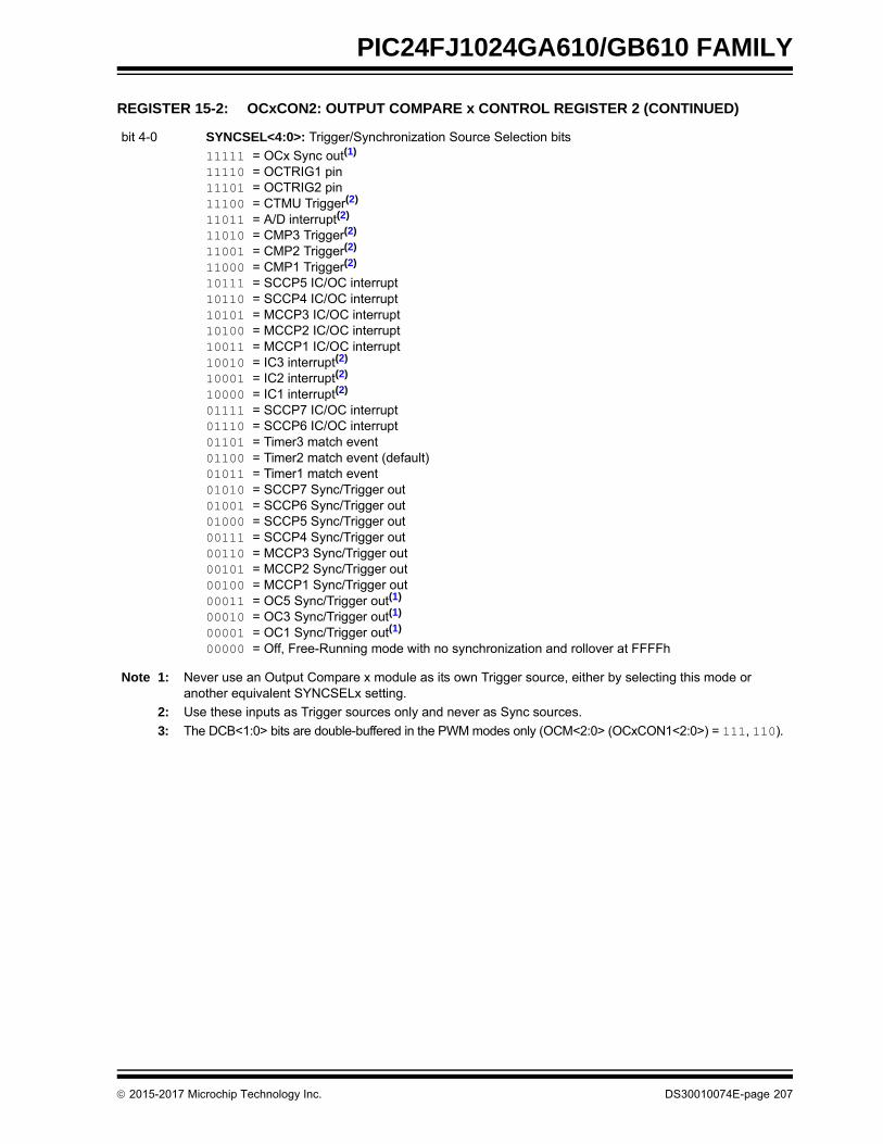
PIC24FJ1024GA610/GB610 FAMILY
bit 4-0 SYNCSEL<4:0>: Trigger/Synchronization Source Selection bits
11111 = OCx Sync out(1)
11110 = OCTRIG1 pin11101 = OCTRIG2 pin11100 = CTMU Trigger(2)
11011 = A/D interrupt(2)
11010 = CMP3 Trigger(2)
11001 = CMP2 Trigger(2)
11000 = CMP1 Trigger(2)
10111 = SCCP5 IC/OC interrupt10110 = SCCP4 IC/OC interrupt10101 = MCCP3 IC/OC interrupt10100 = MCCP2 IC/OC interrupt10011 = MCCP1 IC/OC interrupt10010 = IC3 interrupt(2)
10001 = IC2 interrupt(2)
10000 = IC1 interrupt(2)
01111 = SCCP7 IC/OC interrupt01110 = SCCP6 IC/OC interrupt01101 = Timer3 match event01100 = Timer2 match event (default)01011 = Timer1 match event01010 = SCCP7 Sync/Trigger out01001 = SCCP6 Sync/Trigger out01000 = SCCP5 Sync/Trigger out00111 = SCCP4 Sync/Trigger out00110 = MCCP3 Sync/Trigger out00101 = MCCP2 Sync/Trigger out00100 = MCCP1 Sync/Trigger out00011 = OC5 Sync/Trigger out(1)
00010 = OC3 Sync/Trigger out(1)
00001 = OC1 Sync/Trigger out(1)
00000 = Off, Free-Running mode with no synchronization and rollover at FFFFh
REGISTER 15-2: OCxCON2: OUTPUT COMPARE x CONTROL REGISTER 2 (CONTINUED)
Note 1: Never use an Output Compare x module as its own Trigger source, either by selecting this mode or another equivalent SYNCSELx setting.
2: Use these inputs as Trigger sources only and never as Sync sources.
3: The DCB<1:0> bits are double-buffered in the PWM modes only (OCM<2:0> (OCxCON1<2:0>) = 111, 110).
2015-2017 Microchip Technology Inc. DS30010074E-page 207

PIC24FJ1024GA610/GB610 FAMILY
NOTES:
DS30010074E-page 208 2015-2017 Microchip Technology Inc.

PIC24FJ1024GA610/GB610 FAMILY
16.0 CAPTURE/COMPARE/PWM/TIMER MODULES (MCCP AND SCCP)
PIC24FJ1024GA610/GB610 family devices includeseveral Capture/Compare/PWM/Timer base modules,which provide the functionality of three differentperipherals of earlier PIC24F devices. The module canoperate in one of three major modes:
• General Purpose Timer• Input Capture• Output Compare/PWM
The module is provided in two different forms, distin-guished by the number of PWM outputs that themodule can generate. Single Capture/Compare/PWM(SCCPs) output modules provide only one PWM out-put. Multiple Capture/Compare/PWM (MCCPs) outputmodules can provide up to six outputs and an extendedrange of power control features, depending on the pincount of the particular device. All other features of themodules are identical.
The SCCPx and MCCPx modules can be operatedonly in one of the three major modes at any time. Theother modes are not available unless the module isreconfigured for the new mode.
A conceptual block diagram for the module is shown inFigure 16-1. All three modules share a time base genera-tor and a common Timer register pair (CCPxTMRH/L);other shared hardware components are added as aparticular mode requires.
Each module has a total of 8 control and status registers:
• CCPxCON1L (Register 16-1)
• CCPxCON1H (Register 16-2)
• CCPxCON2L (Register 16-3)
• CCPxCON2H (Register 16-4)
• CCPxCON3L (Register 16-5)
• CCPxCON3H (Register 16-6)
• CCPxSTATL (Register 16-7)
• CCPxSTATH (Register 16-8)
Each module also includes 8 buffer/counter registers thatserve as Timer Value registers or data holding buffers:
• CCPxTMRH/CCPxTMRL (Timer High/Low Counters)
• CCPxPRH/CCPxPRL (Timer Period High/Low)
• CCPxRA (Primary Output Compare Data Buffer)
• CCPxRB (Secondary Output Compare Data Buffer)
• CCPxBUFH/CCPxBUFL (Input Capture High/Low Buffers)
FIGURE 16-1: MCCPx/SCCPx CONCEPTUAL BLOCK DIAGRAM
Note: This data sheet summarizes the featuresof this group of PIC24F devices. It isnot intended to be a comprehensivereference source. For more informationon the MCCP/SCCP modules, refer tothe “dsPIC33/PIC24 Family ReferenceManual”, “Capture/Compare/PWM/Timer(MCCP and SCCP)” (DS33035A), whichis available from the Microchip web site(www.microchip.com). The information inthis data sheet supersedes theinformation in the FRM.
ClockSources
Input Capture
Output
Compare/PWM
T32
CCSELMOD<3:0>
Sync andGatingSources
16/32-Bit
Auxiliary Output (to CTMU)
CCPxIF
CCTxIF
External
Compare/PWMOutput(s)
OEFA/OEFBTimer
Sync/Trigger Out
Special Trigger (to A/D)Capture Input
Time BaseGenerator
CCPxTMRH/L
2015-2017 Microchip Technology Inc. DS30010074E-page 209
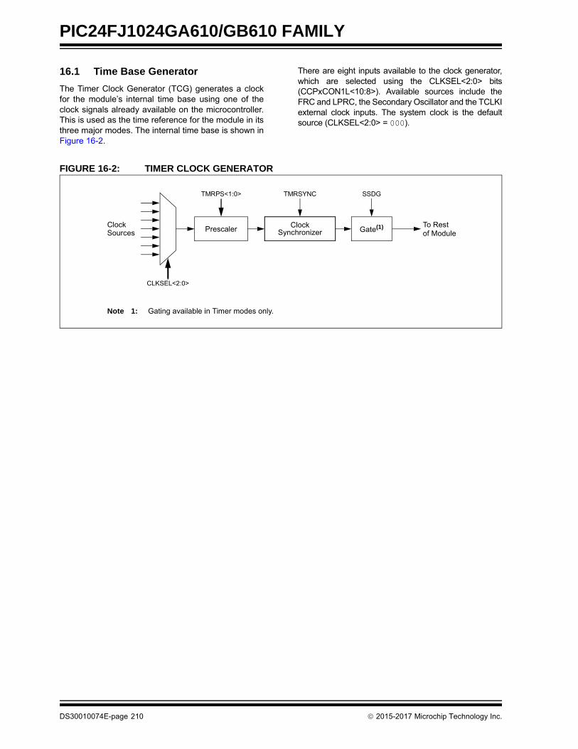
PIC24FJ1024GA610/GB610 FAMILY
16.1 Time Base Generator
The Timer Clock Generator (TCG) generates a clockfor the module’s internal time base using one of theclock signals already available on the microcontroller.This is used as the time reference for the module in itsthree major modes. The internal time base is shown inFigure 16-2.
There are eight inputs available to the clock generator,which are selected using the CLKSEL<2:0> bits(CCPxCON1L<10:8>). Available sources include theFRC and LPRC, the Secondary Oscillator and the TCLKIexternal clock inputs. The system clock is the defaultsource (CLKSEL<2:0> = 000).
FIGURE 16-2: TIMER CLOCK GENERATOR
CLKSEL<2:0>
TMRPS<1:0>
PrescalerClock
Synchronizer
TMRSYNC
Gate(1)
SSDG
ClockSources
To Restof Module
Note 1: Gating available in Timer modes only.
DS30010074E-page 210 2015-2017 Microchip Technology Inc.
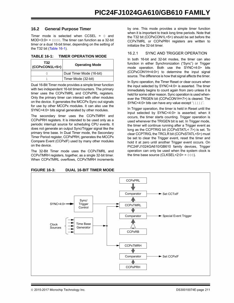
PIC24FJ1024GA610/GB610 FAMILY
16.2 General Purpose Timer
Timer mode is selected when CCSEL = 0 andMOD<3:0> = 0000. The timer can function as a 32-bittimer or a dual 16-bit timer, depending on the setting ofthe T32 bit (Table 16-1).
TABLE 16-1: TIMER OPERATION MODE
Dual 16-Bit Timer mode provides a simple timer functionwith two independent 16-bit timer/counters. The primarytimer uses the CCPxTMRL and CCPxPRL registers.Only the primary timer can interact with other moduleson the device. It generates the MCCPx Sync out signalsfor use by other MCCPx modules. It can also use theSYNC<4:0> bits signal generated by other modules.
The secondary timer uses the CCPxTMRH andCCPxPRH registers. It is intended to be used only as aperiodic interrupt source for scheduling CPU events. Itdoes not generate an output Sync/Trigger signal like theprimary time base. In Dual Timer mode, the SecondaryTimer Period register, CCPxPRH, generates the MCCPxCompare Event (CCPxIF) used by many other moduleson the device.
The 32-Bit Timer mode uses the CCPxTMRL andCCPxTMRH registers, together, as a single 32-bit timer.When CCPxTMRL overflows, CCPxTMRH increments
by one. This mode provides a simple timer functionwhen it is important to track long time periods. Note thatthe T32 bit (CCPxCON1L<5>) should be set before theCCPxTMRL or CCPxPRH registers are written toinitialize the 32-bit timer.
16.2.1 SYNC AND TRIGGER OPERATION
In both 16-bit and 32-bit modes, the timer can alsofunction in either Synchronization (“Sync”) or Triggermode operation. Both use the SYNC<4:0> bits(CCPxCON1H<4:0>) to determine the input signalsource. The difference is how that signal affects the timer.
In Sync operation, the Timer Reset or clear occurs whenthe input selected by SYNC<4:0> is asserted. The timerimmediately begins to count again from zero unless it isheld for some other reason. Sync operation is used when-ever the TRIGEN bit (CCPxCON1H<7>) is cleared. TheSYNC<4:0> bits can have any value except ‘11111’.
In Trigger operation, the timer is held in Reset until theinput selected by SYNC<4:0> is asserted; when itoccurs, the timer starts counting. Trigger operation isused whenever the TRIGEN bit is set. In Trigger mode,the timer will continue running after a Trigger event aslong as the CCPTRIG bit (CCPxSTATL< 7>) is set. Toclear CCPTRIG, the TRCLR bit (CCPxSTATL<5>) mustbe set to clear the Trigger event, reset the timer andhold it at zero until another Trigger event occurs. OnPIC24FJ1024GA610/GB610 family devices, Triggeroperation can only be used when the system clock isthe time base source (CLKSEL<2:0> = 000).
FIGURE 16-3: DUAL 16-BIT TIMER MODE
T32 (CCPxCON1L<5>)
Operating Mode
0 Dual Timer Mode (16-bit)
1 Timer Mode (32-bit)
Comparator
CCPxTMRL
CCPxPRL
CCPxRB
CCPxTMRH
CCPxPRH
Comparator
ClockSources
Set CCTxIF
Special Event Trigger
Set CCPxIF
SYNC<4:0>
Time BaseGenerator
Sync/TriggerControl
Comparator
2015-2017 Microchip Technology Inc. DS30010074E-page 211

PIC24FJ1024GA610/GB610 FAMILY
FIGURE 16-4: 32-BIT TIMER MODE
16.3 Output Compare Mode
Output Compare mode compares the Timer registervalue with the value of one or two Compare registers,depending on its mode of operation. The OutputCompare x module, on compare match events, has theability to generate a single output transition or a train of
output pulses. Like most PIC® MCU peripherals, theOutput Compare x module can also generate interruptson a compare match event.
Table 16-2 shows the various modes available inOutput Compare modes.
TABLE 16-2: OUTPUT COMPARE/PWM MODES
CCPxTMRL
CCPxPRL
Comparator Set CCTxIF
CCPxTMRH
CCPxPRH
ClockSources
Sync/TriggerControl
SYNC<4:0>
Time BaseGenerator
MOD<3:0> (CCPxCON1L<3:0>)
T32 (CCPxCON1L<5>)
Operating Mode
0001 0 Output High on Compare (16-bit)
Single Edge Mode
0001 1 Output High on Compare (32-bit)
0010 0 Output Low on Compare (16-bit)
0010 1 Output Low on Compare (32-bit)
0011 0 Output Toggle on Compare (16-bit)
0011 1 Output Toggle on Compare (32-bit)
0100 0 Dual Edge Compare (16-bit) Dual Edge Mode
0101 0 Dual Edge Compare (16-bit buffered) PWM Mode
0110 0 Center-Aligned Pulse (16-bit buffered) Center PWM Mode
0111 0 Variable Frequency Pulse (16-bit)
1111 0 External Input Source Mode (16-bit)
DS30010074E-page 212 2015-2017 Microchip Technology Inc.

PIC24FJ1024GA610/GB610 FAMILY
FIGURE 16-5: OUTPUT COMPARE x BLOCK DIAGRAM
CCPxRA Buffer
Comparator
CCPxCON1H/L
CCPxCON2H/L
OCx Output,
Output Compare
CCPx Pin(s)
CCPxRB Buffer
Comparator
Fault Logic
Match
Match
Time BaseGenerator
Increment
Reset
OCx ClockSources
Trigger andSync Sources
Reset
Match EventOCFA/OCFB
CCPxRAH/L
Event
Event
Rollover
Rollover/Reset
Rollover/Reset
CCPxCON3H/L
Auto-Shutdown
and Polarity
ControlEdgeDetect
Interrupt
Comparator
Trigger andSync Logic
CCPxPRL
CCPxRBH/L
CCPxTMRH/L
2015-2017 Microchip Technology Inc. DS30010074E-page 213

PIC24FJ1024GA610/GB610 FAMILY
16.4 Input Capture Mode
Input Capture mode is used to capture a timer valuefrom an independent timer base upon an event on aninput pin or other internal Trigger source. The inputcapture features are useful in applications requiringfrequency (time period) and pulse measurement.Figure 16-6 depicts a simplified block diagram of theInput Capture mode.
Input Capture mode uses a dedicated 16/32-bit, synchro-nous, up counting timer for the capture function. The timervalue is written to the FIFO when a capture event occurs.The internal value may be read (with a synchronizationdelay) using the CCPxTMRH/L registers.
To use Input Capture mode, the CCSEL bit(CCPxCON1L<4>) must be set. The T32 andMOD<3:0> bits are used to select the proper Capturemode, as shown in Table 16-3.
FIGURE 16-6: INPUT CAPTURE x BLOCK DIAGRAM
TABLE 16-3: INPUT CAPTURE MODES
MOD<3:0> (CCPxCON1L<3:0>)
T32 (CCPxCON1L<5>)
Operating Mode
0000 0 Edge Detect (16-bit capture)
0000 1 Edge Detect (32-bit capture)
0001 0 Every Rising (16-bit capture)
0001 1 Every Rising (32-bit capture)
0010 0 Every Falling (16-bit capture)
0010 1 Every Falling (32-bit capture)
0011 0 Every Rise/Fall (16-bit capture)
0011 1 Every Rise/Fall (32-bit capture)
0100 0 Every 4th Rising (16-bit capture)
0100 1 Every 4th Rising (32-bit capture)
0101 0 Every 16th Rising (16-bit capture)
0101 1 Every 16th Rising (32-bit capture)
CCPxBUFx
4-Level FIFO Buffer
MOD<3:0>
Set CCPxIF
OPS<3:0>
InterruptLogic
System Bus
Event and
Trigger andSync Logic
ClockSelect
ICx ClockSources
Trigger andSync Sources
ICS<2:0>
16
16
16CCPxTMRH/L
Increment
Reset
T32
Edge Detect Logicand
Clock Synchronizer
DS30010074E-page 214 2015-2017 Microchip Technology Inc.
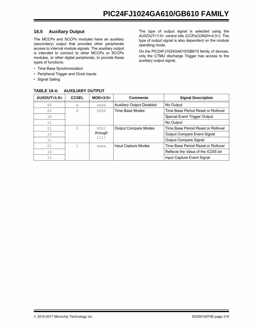
PIC24FJ1024GA610/GB610 FAMILY
16.5 Auxiliary Output
The MCCPx and SCCPx modules have an auxiliary(secondary) output that provides other peripheralsaccess to internal module signals. The auxiliary outputis intended to connect to other MCCPx or SCCPxmodules, or other digital peripherals, to provide thesetypes of functions:
• Time Base Synchronization
• Peripheral Trigger and Clock Inputs
• Signal Gating
The type of output signal is selected using theAUXOUT<1:0> control bits (CCPxCON2H<4:3>). Thetype of output signal is also dependent on the moduleoperating mode.
On the PIC24FJ1024GA610/GB610 family of devices,only the CTMU discharge Trigger has access to theauxiliary output signal.
TABLE 16-4: AUXILIARY OUTPUT
AUXOUT<1:0> CCSEL MOD<3:0> Comments Signal Description
00 x xxxx Auxiliary Output Disabled No Output
01 0 0000 Time Base Modes Time Base Period Reset or Rollover
10 Special Event Trigger Output
11 No Output
01 0 0001through1111
Output Compare Modes Time Base Period Reset or Rollover
10 Output Compare Event Signal
11 Output Compare Signal
01 1 xxxx Input Capture Modes Time Base Period Reset or Rollover
10 Reflects the Value of the ICDIS bit
11 Input Capture Event Signal
2015-2017 Microchip Technology Inc. DS30010074E-page 215

PIC24FJ1024GA610/GB610 FAMILY
REGISTER 16-1: CCPxCON1L: CCPx CONTROL 1 LOW REGISTERS
R/W-0 U-0 R/W-0 R/W-0 R/W-0 R/W-0 R/W-0 R/W-0
CCPON — CCPSIDL CCPSLP TMRSYNC CLKSEL2 CLKSEL1 CLKSEL0
bit 15 bit 8
R/W-0 R/W-0 R/W-0 R/W-0 R/W-0 R/W-0 R/W-0 R/W-0
TMRPS1 TMRPS0 T32 CCSEL MOD3 MOD2 MOD1 MOD0
bit 7 bit 0
Legend:
R = Readable bit W = Writable bit U = Unimplemented bit, read as ‘0’
-n = Value at POR ‘1’ = Bit is set ‘0’ = Bit is cleared x = Bit is unknown
bit 15 CCPON: CCPx Module Enable bit
1 = Module is enabled with an operating mode specified by the MOD<3:0> control bits0 = Module is disabled
bit 14 Unimplemented: Read as ‘0’
bit 13 CCPSIDL: CCPx Stop in Idle Mode Bit
1 = Discontinues module operation when device enters Idle mode0 = Continues module operation in Idle mode
bit 12 CCPSLP: CCPx Sleep Mode Enable bit
1 = Module continues to operate in Sleep modes0 = Module does not operate in Sleep modes
bit 11 TMRSYNC: Time Base Clock Synchronization bit
1 = Module time base clock is synchronized to the internal system clocks; timing restrictions apply0 = Module time base clock is not synchronized to the internal system clocks
bit 10-8 CLKSEL<2:0>: CCPx Time Base Clock Select bits
111 = TCKIA pin110 = TCKIB pin101 = PLL clock100 = 2x peripheral clock010 = SOSC clock001 = Reference clock output000 = System clock
For MCCP1 and SCCP4:011 = CLC1 output
For MCCP2 and SCCP5:011 = CLC2 output
For MCCP3 and SCCP6:011 = CLC3 output
For SCCP7:011 = CLC4 output
bit 7-6 TMRPS<1:0>: Time Base Prescale Select bits
11 = 1:64 Prescaler10 = 1:16 Prescaler01 = 1:4 Prescaler00 = 1:1 Prescaler
bit 5 T32: 32-Bit Time Base Select bit
1 = Uses 32-bit time base for timer, single edge output compare or input capture function0 = Uses 16-bit time base for timer, single edge output compare or input capture function
DS30010074E-page 216 2015-2017 Microchip Technology Inc.
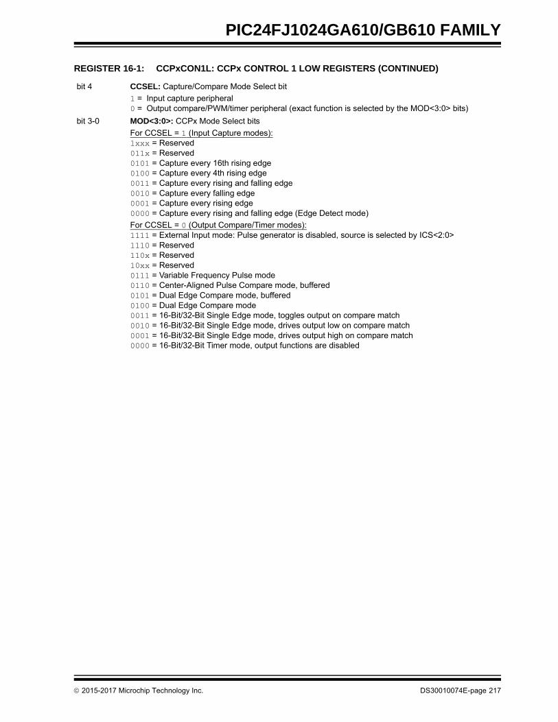
PIC24FJ1024GA610/GB610 FAMILY
bit 4 CCSEL: Capture/Compare Mode Select bit
1 = Input capture peripheral0 = Output compare/PWM/timer peripheral (exact function is selected by the MOD<3:0> bits)
bit 3-0 MOD<3:0>: CCPx Mode Select bits
For CCSEL = 1 (Input Capture modes):1xxx = Reserved011x = Reserved0101 = Capture every 16th rising edge0100 = Capture every 4th rising edge0011 = Capture every rising and falling edge0010 = Capture every falling edge0001 = Capture every rising edge0000 = Capture every rising and falling edge (Edge Detect mode)
For CCSEL = 0 (Output Compare/Timer modes):1111 = External Input mode: Pulse generator is disabled, source is selected by ICS<2:0>1110 = Reserved110x = Reserved10xx = Reserved0111 = Variable Frequency Pulse mode0110 = Center-Aligned Pulse Compare mode, buffered0101 = Dual Edge Compare mode, buffered0100 = Dual Edge Compare mode0011 = 16-Bit/32-Bit Single Edge mode, toggles output on compare match0010 = 16-Bit/32-Bit Single Edge mode, drives output low on compare match0001 = 16-Bit/32-Bit Single Edge mode, drives output high on compare match0000 = 16-Bit/32-Bit Timer mode, output functions are disabled
REGISTER 16-1: CCPxCON1L: CCPx CONTROL 1 LOW REGISTERS (CONTINUED)
2015-2017 Microchip Technology Inc. DS30010074E-page 217

PIC24FJ1024GA610/GB610 FAMILY
REGISTER 16-2: CCPxCON1H: CCPx CONTROL 1 HIGH REGISTERS
R/W-0 R/W-0 U-0 U-0 R/W-0 R/W-0 R/W-0 R/W-0
OPSSRC(1) RTRGEN(2) — — OPS3(3) OPS2(3) OPS1(3) OPS0(3)
bit 15 bit 8
R/W-0 R/W-0 R/W-0 R/W-0 R/W-0 R/W-0 R/W-0 R/W-0
TRIGEN ONESHOT ALTSYNC SYNC4 SYNC3 SYNC2 SYNC1 SYNC0
bit 7 bit 0
Legend:
R = Readable bit W = Writable bit U = Unimplemented bit, read as ‘0’
-n = Value at POR ‘1’ = Bit is set ‘0’ = Bit is cleared x = Bit is unknown
bit 15 OPSSRC: Output Postscaler Source Select bit(1)
1 = Output postscaler scales module Trigger output events0 = Output postscaler scales time base interrupt events
bit 14 RTRGEN: Retrigger Enable bit(2)
1 = Time base can be retriggered when TRIGEN bit = 10 = Time base may not be retriggered when TRIGEN bit = 1
bit 13-12 Unimplemented: Read as ‘0’
bit 11-8 OPS3<3:0>: CCPx Interrupt Output Postscale Select bits(3)
1111 = Interrupt every 16th time base period match1110 = Interrupt every 15th time base period match. . .0100 = Interrupt every 5th time base period match0011 = Interrupt every 4th time base period match or 4th input capture event0010 = Interrupt every 3rd time base period match or 3rd input capture event0001 = Interrupt every 2nd time base period match or 2nd input capture event0000 = Interrupt after each time base period match or input capture event
bit 7 TRIGEN: CCPx Trigger Enable bit
1 = Trigger operation of time base is enabled0 = Trigger operation of time base is disabled
bit 6 ONESHOT: One-Shot Mode Enable bit
1 = One-Shot Trigger mode is enabled; Trigger duration is set by OSCNT<2:0>0 = One-Shot Trigger mode is disabled
bit 5 ALTSYNC: CCPx Clock Select bit
1 = An alternate signal is used as the module synchronization output signal 0 = The module synchronization output signal is the Time Base Reset/rollover event
bit 4-0 SYNC<4:0>: CCPx Synchronization Source Select bits
See Table 16-5 for the definition of inputs.
Note 1: This control bit has no function in Input Capture modes.
2: This control bit has no function when TRIGEN = 0.
3: Output postscale settings, from 1:5 to 1:16 (0100-1111), will result in a FIFO buffer overflow for Input Capture modes.
DS30010074E-page 218 2015-2017 Microchip Technology Inc.
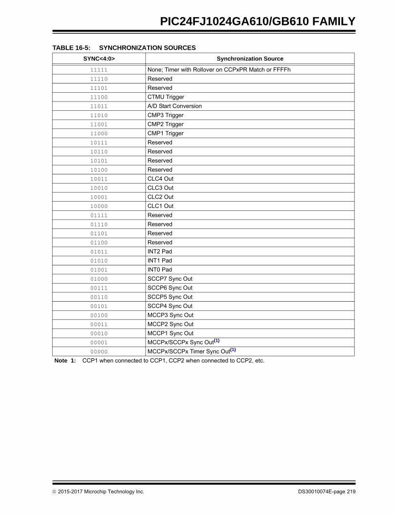
PIC24FJ1024GA610/GB610 FAMILY
TABLE 16-5: SYNCHRONIZATION SOURCES
SYNC<4:0> Synchronization Source
11111 None; Timer with Rollover on CCPxPR Match or FFFFh
11110 Reserved
11101 Reserved
11100 CTMU Trigger
11011 A/D Start Conversion
11010 CMP3 Trigger
11001 CMP2 Trigger
11000 CMP1 Trigger
10111 Reserved
10110 Reserved
10101 Reserved
10100 Reserved
10011 CLC4 Out
10010 CLC3 Out
10001 CLC2 Out
10000 CLC1 Out
01111 Reserved
01110 Reserved
01101 Reserved
01100 Reserved
01011 INT2 Pad
01010 INT1 Pad
01001 INT0 Pad
01000 SCCP7 Sync Out
00111 SCCP6 Sync Out
00110 SCCP5 Sync Out
00101 SCCP4 Sync Out
00100 MCCP3 Sync Out
00011 MCCP2 Sync Out
00010 MCCP1 Sync Out
00001 MCCPx/SCCPx Sync Out(1)
00000 MCCPx/SCCPx Timer Sync Out(1)
Note 1: CCP1 when connected to CCP1, CCP2 when connected to CCP2, etc.
2015-2017 Microchip Technology Inc. DS30010074E-page 219

PIC24FJ1024GA610/GB610 FAMILY
TABLE 16-6: AUTO-SHUTDOWN SOURCES
REGISTER 16-3: CCPxCON2L: CCPx CONTROL 2 LOW REGISTERS
R/W-0 R/W-0 U-0 R/W-0 U-0 U-0 U-0 U-0
PWMRSEN ASDGM — SSDG — — — —
bit 15 bit 8
R/W-0 R/W-0 R/W-0 R/W-0 R/W-0 R/W-0 R/W-0 R/W-0
ASDG7 ASDG6 ASDG5 ASDG4 ASDG3 ASDG2 ASDG1 ASDG0
bit 7 bit 0
Legend:
R = Readable bit W = Writable bit U = Unimplemented bit, read as ‘0’
-n = Value at POR ‘1’ = Bit is set ‘0’ = Bit is cleared x = Bit is unknown
bit 15 PWMRSEN: CCPx PWM Restart Enable bit
1 = ASEVT bit clears automatically at the beginning of the next PWM period, after the shutdown inputhas ended
0 = ASEVT bit must be cleared in software to resume PWM activity on output pins
bit 14 ASDGM: CCPx Auto-Shutdown Gate Mode Enable bit
1 = Waits until the next Time Base Reset or rollover for shutdown to occur0 = Shutdown event occurs immediately
bit 13 Unimplemented: Read as ‘0’
bit 12 SSDG: CCPx Software Shutdown/Gate Control bit
1 = Manually forces auto-shutdown, timer clock gate or input capture signal gate event (setting ofASDGM bit still applies)
0 = Normal module operation
bit 11-8 Unimplemented: Read as ‘0’
bit 7-0 ASDG<7:0>: CCPx Auto-Shutdown/Gating Source Enable bits
1 = ASDGx Source n is enabled (see Table 16-6 for auto-shutdown/gating sources)0 = ASDGx Source n is disabled
ASDG<7:0>Auto-Shutdown Source
MCCP1 MCCP2 MCCP3 SCCP4 SCCP5 SCCP6 SCCP7
1xxx xxxx OCFB
x1xx xxxx OCFA
xx1x xxxx CLC1 CLC2 CLC3 CLC1 CLC2 CLC3 CLC4
xxx1 xxxx SCCP4 OC Out MCCP1 OC Out
xxxx 1xxx SCCP5 OC Out MCCP2 OC Out
xxxx x1xx CMP3 Out
xxxx xx1x CMP2 Out
xxxx xxx1 CMP1 Out
DS30010074E-page 220 2015-2017 Microchip Technology Inc.

PIC24FJ1024GA610/GB610 FAMILY
REGISTER 16-4: CCPxCON2H: CCPx CONTROL 2 HIGH REGISTERS
R/W-0 U-0 R/W-0 R/W-0 R/W-0 R/W-0 R/W-0 R/W-1
OENSYNC — OCFEN(1,2) OCEEN(1,2) OCDEN(1,2) OCCEN(1,2) OCBEN(1) OCAEN
bit 15 bit 8
R/W-0 R/W-0 U-0 R/W-0 R/W-0 R/W-0 R/W-0 R/W-0
ICGSM1 ICGSM0 — AUXOUT1 AUXOUT0 ICS2 ICS1 ICS0
bit 7 bit 0
Legend:
R = Readable bit W = Writable bit U = Unimplemented bit, read as ‘0’
-n = Value at POR ‘1’ = Bit is set ‘0’ = Bit is cleared x = Bit is unknown
bit 15 OENSYNC: Output Enable Synchronization bit
1 = Update by output enable bits occurs on the next Time Base Reset or rollover0 = Update by output enable bits occurs immediately
bit 14 Unimplemented: Read as ‘0’
bit 13-8 OCxEN: Output Enable/Steering Control bits(1,2)
1 = OCMx pin is controlled by the CCPx module and produces an output compare or PWM signal0 = OCMx pin is not controlled by the CCPx module; the pin is available to the port logic or another
peripheral multiplexed on the pin
bit 7-6 ICGSM<1:0>: Input Capture Gating Source Mode Control bits
11 = Reserved10 = One-Shot mode: Falling edge from gating source disables future capture events (ICDIS = 1)01 = One-Shot mode: Rising edge from gating source enables future capture events (ICDIS = 0)00 = Level-Sensitive mode: A high level from gating source will enable future capture events; a low
level will disable future capture events
bit 5 Unimplemented: Read as ‘0’
bit 4-3 AUXOUT<1:0>: Auxiliary Output Signal on Event Selection bits
11 = Input capture or output compare event; no signal in Timer mode10 = Signal output is defined by module operating mode (see Table 16-4)01 = Time base rollover event (all modes)00 = Disabled
bit 2-0 ICS<2:0>: Input Capture Source Select bits
111 = CLC4 output110 = CLC3 output101 = CLC2 output100 = CLC1 output011 = Comparator 3 output010 = Comparator 2 output001 = Comparator 1 output000 = Input Capture x (ICMx) I/O pin
Note 1: OCFEN through OCBEN (bits<13:9>) are implemented in MCCPx modules only.
2: OCFEN through OCCEN (bits<13:10>) are not available on 64-pin parts.
2015-2017 Microchip Technology Inc. DS30010074E-page 221
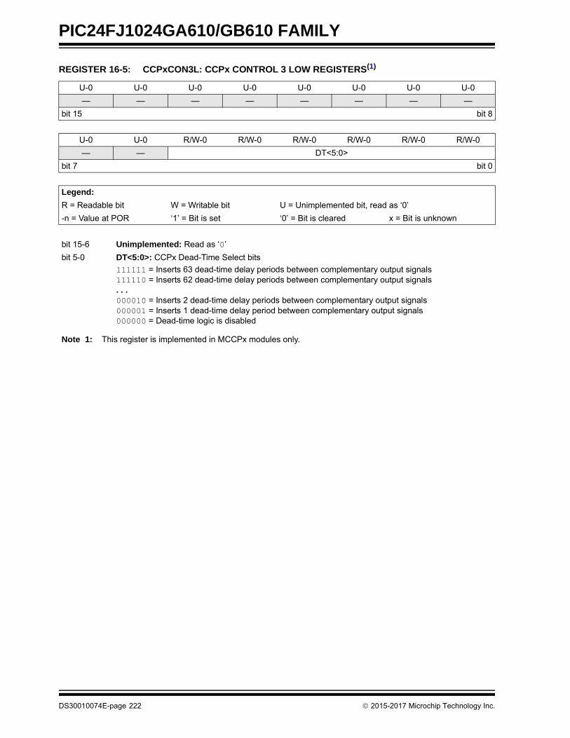
PIC24FJ1024GA610/GB610 FAMILY
REGISTER 16-5: CCPxCON3L: CCPx CONTROL 3 LOW REGISTERS(1)
U-0 U-0 U-0 U-0 U-0 U-0 U-0 U-0
— — — — — — — —
bit 15 bit 8
U-0 U-0 R/W-0 R/W-0 R/W-0 R/W-0 R/W-0 R/W-0
— — DT<5:0>
bit 7 bit 0
Legend:
R = Readable bit W = Writable bit U = Unimplemented bit, read as ‘0’
-n = Value at POR ‘1’ = Bit is set ‘0’ = Bit is cleared x = Bit is unknown
bit 15-6 Unimplemented: Read as ‘0’
bit 5-0 DT<5:0>: CCPx Dead-Time Select bits
111111 = Inserts 63 dead-time delay periods between complementary output signals111110 = Inserts 62 dead-time delay periods between complementary output signals. . .000010 = Inserts 2 dead-time delay periods between complementary output signals000001 = Inserts 1 dead-time delay period between complementary output signals000000 = Dead-time logic is disabled
Note 1: This register is implemented in MCCPx modules only.
DS30010074E-page 222 2015-2017 Microchip Technology Inc.

PIC24FJ1024GA610/GB610 FAMILY
REGISTER 16-6: CCPxCON3H: CCPx CONTROL 3 HIGH REGISTERS
R/W-0 R/W-0 R/W-0 R/W-0 U-0 R/W-0 R/W-0 R/W-0
OETRIG OSCNT2 OSCNT1 OSCNT0 — OUTM2(1) OUTM1(1) OUTM0(1)
bit 15 bit 8
U-0 U-0 R/W-0 R/W-0 R/W-0 R/W-0 R/W-0 R/W-0
— — POLACE POLBDF(1) PSSACE1 PSSACE0 PSSBDF1(1) PSSBDF0(1)
bit 7 bit 0
Legend:
R = Readable bit W = Writable bit U = Unimplemented bit, read as ‘0’
-n = Value at POR ‘1’ = Bit is set ‘0’ = Bit is cleared x = Bit is unknown
bit 15 OETRIG: CCPx Dead-Time Select bit
1 = For Triggered mode (TRIGEN = 1): Module does not drive enabled output pins until triggered0 = Normal output pin operation
bit 14-12 OSCNT<2:0>: One-Shot Event Count bits
111 = Extends one-shot event by 7 time base periods (8 time base periods total)110 = Extends one-shot event by 6 time base periods (7 time base periods total)101 = Extends one-shot event by 5 time base periods (6 time base periods total)100 = Extends one-shot event by 4 time base periods (5 time base periods total)011 = Extends one-shot event by 3 time base periods (4 time base periods total)010 = Extends one-shot event by 2 time base periods (3 time base periods total)001 = Extends one-shot event by 1 time base period (2 time base periods total)000 = Does not extend one-shot Trigger event
bit 11 Unimplemented: Read as ‘0’
bit 10-8 OUTM<2:0>: PWMx Output Mode Control bits(1)
111 = Reserved110 = Output Scan mode101 = Brush DC Output mode, forward100 = Brush DC Output mode, reverse011 = Reserved010 = Half-Bridge Output mode001 = Push-Pull Output mode000 = Steerable Single Output mode
bit 7-6 Unimplemented: Read as ‘0’
bit 5 POLACE: CCPx Output Pins, OCMxA, OCMxC and OCMxE, Polarity Control bit
1 = Output pin polarity is active-low0 = Output pin polarity is active-high
bit 4 POLBDF: CCPx Output Pins, OCMxB, OCMxD and OCMxF, Polarity Control bit(1)
1 = Output pin polarity is active-low0 = Output pin polarity is active-high
bit 3-2 PSSACE<1:0>: PWMx Output Pins, OCMxA, OCMxC and OCMxE, Shutdown State Control bits
11 = Pins are driven active when a shutdown event occurs10 = Pins are driven inactive when a shutdown event occurs0x = Pins are tri-stated when a shutdown event occurs
bit 1-0 PSSBDF<1:0>: PWMx Output Pins, OCMxB, OCMxD, and OCMxF, Shutdown State Control bits(1)
11 = Pins are driven active when a shutdown event occurs10 = Pins are driven inactive when a shutdown event occurs0x = Pins are in a high-impedance state when a shutdown event occurs
Note 1: These bits are implemented in MCCPx modules only.
2015-2017 Microchip Technology Inc. DS30010074E-page 223

PIC24FJ1024GA610/GB610 FAMILY
REGISTER 16-7: CCPxSTATL: CCPx STATUS REGISTER LOW
U-0 U-0 U-0 U-0 U-0 W-0 U-0 U-0
— — — — — ICGARM — —
bit 15 bit 8
R-0 W1-0 W1-0 R/C-0 R/C-0 R/C-0 R/C-0 R/C-0
CCPTRIG TRSET TRCLR ASEVT SCEVT ICDIS ICOV ICBNE
bit 7 bit 0
Legend: C = Clearable bit W = Writable bit
R = Readable bit W1 = Write ‘1’ Only bit U = Unimplemented bit, read as ‘0’
-n = Value at POR ‘1’ = Bit is set ‘0’ = Bit is cleared x = Bit is unknown
bit 15-11 Unimplemented: Read as ‘0’
bit 10 ICGARM: Input Capture Gate Arm bit
A write of ‘1’ to this location will arm the Input Capture x module for a one-shot gating event whenICGSM<1:0> = 01 or 10; read as ‘0’.
bit 9-8 Unimplemented: Read as ‘0’
bit 7 CCPTRIG: CCPx Trigger Status bit
1 = Timer has been triggered and is running0 = Timer has not been triggered and is held in Reset
bit 6 TRSET: CCPx Trigger Set Request bit
Write ‘1’ to this location to trigger the timer when TRIGEN = 1 (location always reads as ‘0’).
bit 5 TRCLR: CCPx Trigger Clear Request bit
Write ‘1’ to this location to cancel the timer Trigger when TRIGEN = 1 (location always reads as ‘0’).
bit 4 ASEVT: CCPx Auto-Shutdown Event Status/Control bit
1 = A shutdown event is in progress; CCPx outputs are in the shutdown state0 = CCPx outputs operate normally
bit 3 SCEVT: Single Edge Compare Event Status bit
1 = A single edge compare event has occurred0 = A single edge compare event has not occurred
bit 2 ICDIS: Input Capture x Disable bit
1 = Event on Input Capture x pin (ICMx) does not generate a capture event0 = Event on Input Capture x pin will generate a capture event
bit 1 ICOV: Input Capture x Buffer Overflow Status bit
1 = The Input Capture x FIFO buffer has overflowed0 = The Input Capture x FIFO buffer has not overflowed
bit 0 ICBNE: Input Capture x Buffer Status bit
1 = Input Capture x buffer has data available0 = Input Capture x buffer is empty
DS30010074E-page 224 2015-2017 Microchip Technology Inc.

PIC24FJ1024GA610/GB610 FAMILY
REGISTER 16-8: CCPxSTATH: CCPx STATUS REGISTER HIGH
U-0 U-0 U-0 U-0 U-0 U-0 U-0 U-0
— — — — — — — —
bit 15 bit 8
U-0 U-0 U-0 R-0 R-0 R-0 R-0 R-0
— — — PRLWIP TMRHWIP TMRLWIP RBWIP RAWIP
bit 7 bit 0
Legend:
R = Readable bit W = Writable bit U = Unimplemented bit, read as ‘0’
-n = Value at POR ‘1’ = Bit is set ‘0’ = Bit is cleared x = Bit is unknown
bit 15-5 Unimplemented: Read as ‘0’
bit 4 PRLWIP: CCPxPRL Write in Progress Status bit
1 = An update to the CCPxPRL register with the buffered contents is in progress0 = An update to the CCPxPRL register is not in progress
bit 3 TMRHWIP: CCPxTMRH Write in Progress Status Bit
1 = An update to the CCPxTMRH register with the buffered contents is in progress0 = An update to the CCPxTMRH register is not in progress.
bit 2 TMRLWIP: CCPxTMRL Write in Progress Status bit
1 = An update to the CCPxTMRL register with the buffered contents is in progress0 = An update to the CCPxTMRL register is not in progress
bit 1 RBWIP: CCPxRB Write in Progress Status bit
1 = An update to the CCPxRB register with the buffered contents is in progress0 = An update to the CCPxRB register is not in progress
bit 0 RAWIP: CCPxRA Write in Progress Status bit
1 = An update to the CCPxRA register with the buffered contents is in progress0 = An update to the CCPxRA register is not in progress
2015-2017 Microchip Technology Inc. DS30010074E-page 225

PIC24FJ1024GA610/GB610 FAMILY
NOTES:
DS30010074E-page 226 2015-2017 Microchip Technology Inc.

PIC24FJ1024GA610/GB610 FAMILY
17.0 SERIAL PERIPHERAL INTERFACE (SPI)
The Serial Peripheral Interface (SPI) module is asynchronous serial interface useful for communicatingwith other peripheral or microcontroller devices. Theseperipheral devices may be serial EEPROMs, shiftregisters, display drivers, A/D Converters, etc. The SPImodule is compatible with the Motorola® SPI and SIOPinterfaces. All devices in the PIC24FJ1024GA610/GB610 family include three SPI modules.
The module supports operation in two buffer modes. InStandard mode, data is shifted through a single serialbuffer. In Enhanced Buffer mode, data is shiftedthrough a FIFO buffer. The FIFO level depends on theconfigured mode.
Variable length data can be transmitted and receivedfrom 2 to 32 bits.
The module also supports a basic framed SPI protocolwhile operating in either Master or Slave mode. A totalof four framed SPI configurations are supported.
The module also supports Audio modes. Four differentAudio modes are available.
• I2S mode
• Left Justified
• Right Justified
• PCM/DSP
In each of these modes, the serial clock is free-runningand audio data is always transferred.
If an audio protocol data transfer takes place betweentwo devices, then usually one device is the master andthe other is the slave. However, audio data can betransferred between two slaves. Because the audioprotocols require free-running clocks, the master canbe a third party controller. In either case, the mastergenerates two free-running clocks: SCKx and LRC(Left, Right Channel Clock/SSx/FSYNC).
The SPI serial interface consists of four pins:
• SDIx: Serial Data Input
• SDOx: Serial Data Output
• SCKx: Shift Clock Input or Output
• SSx: Active-Low Slave Select or Frame Synchronization I/O Pulse
The SPI module can be configured to operate using 2,3 or 4 pins. In the 3-pin mode, SSx is not used. In the2-pin mode, both SDOx and SSx are not used.
The SPI module has the ability to generate three inter-rupts reflecting the events that occur during the datacommunication. The following types of interrupts canbe generated:
1. Receive interrupts are signalled by SPIxRXIF.This event occurs when:
- RX watermark interrupt
- SPIROV = 1
- SPIRBF = 1
- SPIRBE = 1
provided the respective mask bits are enabled inSPIxIMSKL/H.
2. Transmit interrupts are signalled by SPIxTXIF.This event occurs when:
- TX watermark interrupt
- SPITUR = 1
- SPITBF = 1
- SPITBE = 1
provided the respective mask bits are enabled inSPIxIMSKL/H.
3. General interrupts are signalled by SPIxIF. Thisevent occurs when
- FRMERR = 1
- SPIBUSY = 1
- SRMT = 1
provided the respective mask bits are enabled inSPIxIMSKL/H.
A block diagram of the module in Enhanced Buffer modeis shown in Figure 17-1.
Note: This data sheet summarizes the features ofthe PIC24FJ1024GA610/GB610 family ofdevices. It is not intended to be a compre-hensive reference source. To complementthe information in this data sheet, refer tothe “dsPIC33/PIC24 Family ReferenceManual”, “Serial Peripheral Interface(SPI) with Audio Codec Support”(DS70005136), which is available from theMicrochip web site (www.microchip.com).The information in this data sheetsupersedes the information in the FRM.
Note: Do not perform Read-Modify-Write opera-tions (such as bit-oriented instructions) onthe SPIxBUF register in either Standard orEnhanced Buffer mode.
Note: In this section, the SPI modules arereferred to together as SPIx, or separatelyas SPI1, SPI2 or SPI3. Special FunctionRegisters will follow a similar notation. Forexample, SPIxCON1 and SPIxCON2refer to the control registers for any of thethree SPI modules.
2015-2017 Microchip Technology Inc. DS30010074E-page 227

PIC24FJ1024GA610/GB610 FAMILY
17.1 Master Mode Operation
Perform the following steps to set up the SPIx modulefor Master mode operation:
1. Disable the SPIx interrupts in the respectiveIECx register.
2. Stop and reset the SPIx module by clearing theSPIEN bit.
3. Clear the receive buffer.
4. Clear the ENHBUF bit (SPIxCON1L<0>) if usingStandard Buffer mode or set the bit if usingEnhanced Buffer mode.
5. If SPIx interrupts are not going to be used, skipthis step. Otherwise, the following additionalsteps are performed:
a) Clear the SPIx interrupt flags/events in therespective IFSx register.
b) Write the SPIx interrupt priority andsub-priority bits in the respective IPCxregister.
c) Set the SPIx interrupt enable bits in therespective IECx register.
6. Write the Baud Rate register, SPIxBRGL.
7. Clear the SPIROV bit (SPIxSTATL<6>).
8. Write the desired settings to the SPIxCON1Lregister with MSTEN (SPIxCON1L<5>) = 1.
9. Enable SPI operation by setting the SPIEN bit(SPIxCON1L<15>).
10. Write the data to be transmitted to theSPIxBUFL and SPIxBUFH registers. Transmis-sion (and reception) will start as soon as data iswritten to the SPIxBUFL/H registers.
17.2 Slave Mode Operation
The following steps are used to set up the SPIx modulefor the Slave mode of operation:
1. If using interrupts, disable the SPIx interrupts inthe respective IECx register.
2. Stop and reset the SPIx module by clearing theSPIEN bit.
3. Clear the receive buffer.
4. Clear the ENHBUF bit (SPIxCON1L<0>) if usingStandard Buffer mode or set the bit if usingEnhanced Buffer mode.
5. If using interrupts, the following additional stepsare performed:
a) Clear the SPIx interrupt flags/events in therespective IFSx register.
b) Write the SPIx interrupt priority and sub-priority bits in the respective IPCx register.
c) Set the SPIx interrupt enable bits in therespective IECx register.
6. Clear the SPIROV bit (SPIxSTATL<6>).
7. Write the desired settings to the SPIxCON1Lregister with MSTEN (SPIxCON1L<5>) = 0.
8. Enable SPI operation by setting the SPIEN bit(SPIxCON1L<15>).
9. Transmission (and reception) will start as soonas the master provides the serial clock.
The following additional features are provided inSlave mode:
• Slave Select Synchronization:The SSx pin allows a Synchronous Slave mode. If the SSEN bit (SPIxCON1L<7>) is set, transmis-sion and reception are enabled in Slave mode only if the SSx pin is driven to a low state. The port output or other peripheral outputs must not be driven in order to allow the SSx pin to function as an input. If the SSEN bit is set and the SSx pin is driven high, the SDOx pin is no longer driven and will tri-state, even if the module is in the middle of a transmission. An aborted transmission will be tried again the next time the SSx pin is driven low using the data held in the SPIxTXB register. If the SSEN bit is not set, the SSx pin does not affect the module operation in Slave mode.
• SPITBE Status Flag Operation:The SPITBE bit (SPIxSTATL<3>) has a different function in the Slave mode of operation. The following describes the function of SPITBE for various settings of the Slave mode of operation:
- If SSEN (SPIxCON1L<7>) is cleared, the SPITBE bit is cleared when SPIxBUF is loaded by the user code. It is set when the module transfers SPIxTXB to SPIxTXSR.This is similar to the SPITBE bit function in Master mode.
- If SSEN is set, SPITBE is cleared when SPIxBUF is loaded by the user code. How-ever, it is set only when the SPIx module completes data transmission. A transmission will be aborted when the SSx pin goes high and may be retried at a later time. So, each data word is held in SPIxTXB until all bits are transmitted to the receiver.
DS30010074E-page 228 2015-2017 Microchip Technology Inc.

PIC24FJ1024GA610/GB610 FAMILY
FIGURE 17-1: SPIx MODULE BLOCK DIAGRAM (ENHANCED MODE)
17.3 Audio Mode Operation
To initialize the SPIx module for Audio mode, follow thesteps to initialize it for Master/Slave mode, but also setthe AUDEN bit (SPIxCON1H<15>). In Master+Audiomode:
• This mode enables the device to generate SCKx and LRC pulses as long as the SPIEN bit (SPIxCON1L<15>) = 1.
• The SPIx module generates LRC and SCKx continuously in all cases, regardless of the transmit data, while in Master mode.
• The SPIx module drives the leading edge of LRC and SCKx within 1 SCKx period, and the serial data shifts in and out continuously, even when the TX FIFO is empty.
In Slave+Audio mode:
• This mode enables the device to receive SCKx and LRC pulses as long as the SPIEN bit (SPIxCON1L<15>) = 1.
• The SPIx module drives zeros out of SDOx, but does not shift data out or in (SDIx) until the module receives the LRC (i.e., the edge that precedes the left channel).
• Once the module receives the leading edge of LRC, it starts receiving data if DISSDI (SPIxCON1L<4>) = 0 and the serial data shifts out continuously, even when the TX FIFO is empty.
Read Write
InternalData Bus
SDIx
SDOx
SSx/FSYNC
SCKx
MSB
ShiftControl
EdgeSelect
Enable Master Clock
Transmit
PBCLK
MCLK
MCLKEN
SPIxRXSR
URDTEN
1
0
TXELM<5:0> = 6’b0
MSB
Baud RateGenerator
SSx & FSYNCControl
ClockControl
SPIxTXSR
ClockControl
Receive
SPIxURDTSPIxTXB
EdgeSelect
SPIxRXB
2015-2017 Microchip Technology Inc. DS30010074E-page 229

PIC24FJ1024GA610/GB610 FAMILY
17.4 SPI Control Registers
REGISTER 17-1: SPIxCON1L: SPIx CONTROL REGISTER 1 LOW
R/W-0 U-0 R/W-0 R/W-0 R/W-0 R/W-0 R/W-0 R/W-0
SPIEN — SPISIDL DISSDO MODE32(1,4) MODE16(1,4) SMP CKE(1)
bit 15 bit 8
R/W-0 R/W-0 R/W-0 R/W-0 R/W-0 R/W-0 R/W-0 R/W-0
SSEN(2) CKP MSTEN DISSDI DISSCK MCLKEN(3) SPIFE ENHBUF
bit 7 bit 0
Legend:
R = Readable bit W = Writable bit U = Unimplemented bit, read as ‘0’
-n = Value at POR ‘1’ = Bit is set ‘0’ = Bit is cleared x = Bit is unknown
bit 15 SPIEN: SPIx On bit
1 = Enables module0 = Turns off and resets module, disables clocks, disables interrupt event generation, allows SFR
modifications
bit 14 Unimplemented: Read as ‘0’
bit 13 SPISIDL: SPIx Stop in Idle Mode bit
1 = Halts in CPU Idle mode0 = Continues to operate in CPU Idle mode
bit 12 DISSDO: Disable SDOx Output Port bit
1 = SDOx pin is not used by the module; pin is controlled by the port function0 = SDOx pin is controlled by the module
bit 11-10 MODE<32,16>: Serial Word Length bits(1,4)
AUDEN = 0:MODE32 MODE16 COMMUNICATION1 x 32-Bit0 1 16-Bit0 0 8-Bit
AUDEN = 1:MODE32 MODE16 COMMUNICATION1 1 24-Bit Data, 32-Bit FIFO, 32-Bit Channel/64-Bit Frame1 0 32-Bit Data, 32-Bit FIFO, 32-Bit Channel/64-Bit Frame0 1 16-Bit Data, 16-Bit FIFO, 32-Bit Channel/64-Bit Frame0 0 16-Bit Data, 16-Bit FIFO, 16-Bit Channel/32-Bit Frame
bit 9 SMP: SPIx Data Input Sample Phase bit
Master Mode:1 = Input data is sampled at the end of data output time0 = Input data is sampled at the middle of data output time
Slave Mode:Input data is always sampled at the middle of data output time, regardless of the SMP setting.
Note 1: When AUDEN = 1, this module functions as if CKE = 0, regardless of its actual value.
2: When FRMEN = 1, SSEN is not used.
3: MCLKEN can only be written when the SPIEN bit = 0.
4: This channel is not meaningful for DSP/PCM mode as LRC follows the FRMSYPW bit.
DS30010074E-page 230 2015-2017 Microchip Technology Inc.

PIC24FJ1024GA610/GB610 FAMILY
bit 8 CKE: SPIx Clock Edge Select bit(1)
1 = Transmit happens on transition from active clock state to Idle clock state0 = Transmit happens on transition from Idle clock state to active clock state
bit 7 SSEN: Slave Select Enable bit (Slave mode)(2)
1 = SSx pin is used by the macro in Slave mode; SSx pin is used as the slave select input0 = SSx pin is not used by the macro (SSx pin will be controlled by the port I/O)
bit 6 CKP: SPIx Clock Polarity Select bit
1 = Idle state for clock is a high level; active state is a low level0 = Idle state for clock is a low level; active state is a high level
bit 5 MSTEN: Master Mode Enable bit
1 = Master mode0 = Slave mode
bit 4 DISSDI: Disable SDIx Input Port bit
1 = SDIx pin is not used by the module; pin is controlled by the port function0 = SDIx pin is controlled by the module
bit 3 DISSCK: Disable SCKx Output Port bit
1 = SCKx pin is not used by the module; pin is controlled by the port function0 = SCKx pin is controlled by the module
bit 2 MCLKEN: Master Clock Enable bit(3)
1 = REFO output is used by the BRG0 = Peripheral clock is used by the BRG
bit 1 SPIFE: Frame Sync Pulse Edge Select bit
1 = Frame Sync pulse (Idle-to-active edge) coincides with the first bit clock0 = Frame Sync pulse (Idle-to-active edge) precedes the first bit clock
bit 0 ENHBUF: Enhanced Buffer Mode Enable bit
1 = Enhanced Buffer mode is enabled 0 = Enhanced Buffer mode is disabled
REGISTER 17-1: SPIxCON1L: SPIx CONTROL REGISTER 1 LOW (CONTINUED)
Note 1: When AUDEN = 1, this module functions as if CKE = 0, regardless of its actual value.
2: When FRMEN = 1, SSEN is not used.
3: MCLKEN can only be written when the SPIEN bit = 0.
4: This channel is not meaningful for DSP/PCM mode as LRC follows the FRMSYPW bit.
2015-2017 Microchip Technology Inc. DS30010074E-page 231

PIC24FJ1024GA610/GB610 FAMILY
REGISTER 17-2: SPIxCON1H: SPIx CONTROL REGISTER 1 HIGH
R/W-0 R/W-0 R/W-0 R/W-0 R/W-0 R/W-0 R/W-0 R/W-0
AUDEN(1) SPISGNEXT IGNROV IGNTUR AUDMONO(2) URDTEN(3) AUDMOD1(4) AUDMOD0(4)
bit 15 bit 8
R/W-0 R/W-0 R/W-0 R/W-0 R/W-0 R/W-0 R/W-0 R/W-0
FRMEN FRMSYNC FRMPOL MSSEN FRMSYPW FRMCNT2 FRMCNT1 FRMCNT0
bit 7 bit 0
Legend:
R = Readable bit W = Writable bit U = Unimplemented bit, read as ‘0’
-n = Value at POR ‘1’ = Bit is set ‘0’ = Bit is cleared x = Bit is unknown
bit 15 AUDEN: Audio Codec Support Enable bit(1)
1 = Audio protocol is enabled; MSTEN controls the direction of both the SCKx and Frame (a.k.a. LRC),and this module functions as if FRMEN = 1, FRMSYNC = MSTEN, FRMCNT<2:0> = 001 andSMP = 0, regardless of their actual values
0 = Audio protocol is disabled
bit 14 SPISGNEXT: SPIx Sign-Extend RX FIFO Read Data Enable bit
1 = Data from RX FIFO is sign-extended0 = Data from RX FIFO is not sign-extended
bit 13 IGNROV: Ignore Receive Overflow bit
1 = A Receive Overflow (ROV) is NOT a critical error; during ROV, data in the FIFO is not overwrittenby the receive data
0 = A ROV is a critical error that stops SPI operation
bit 12 IGNTUR: Ignore Transmit Underrun bit
1 = A Transmit Underrun (TUR) is NOT a critical error and data indicated by URDTEN is transmitteduntil the SPIxTXB is not empty
0 = A TUR is a critical error that stops SPI operation
bit 11 AUDMONO: Audio Data Format Transmit bit(2)
1 = Audio data is mono (i.e., each data word is transmitted on both left and right channels)0 = Audio data is stereo
bit 10 URDTEN: Transmit Underrun Data Enable bit(3)
1 = Transmits data out of SPIxURDTL/H register during Transmit Underrun conditions0 = Transmits the last received data during Transmit Underrun conditions
bit 9-8 AUDMOD<1:0>: Audio Protocol Mode Selection bits(4)
11 = PCM/DSP mode10 = Right Justified mode: This module functions as if SPIFE = 1, regardless of its actual value01 = Left Justified mode: This module functions as if SPIFE = 1, regardless of its actual value00 = I2S mode: This module functions as if SPIFE = 0, regardless of its actual value
bit 7 FRMEN: Framed SPIx Support bit
1 = Framed SPIx support is enabled (SSx pin is used as the FSYNC input/output)0 = Framed SPIx support is disabled
Note 1: AUDEN can only be written when the SPIEN bit = 0.2: AUDMONO can only be written when the SPIEN bit = 0 and is only valid for AUDEN = 1.3: URDTEN is only valid when IGNTUR = 1.
4: AUDMOD<1:0> bits can only be written when the SPIEN bit = 0 and are only valid when AUDEN = 1. When NOT in PCM/DSP mode, this module functions as if FRMSYPW = 1, regardless of its actual value.
DS30010074E-page 232 2015-2017 Microchip Technology Inc.

PIC24FJ1024GA610/GB610 FAMILY
bit 6 FRMSYNC: Frame Sync Pulse Direction Control bit
1 = Frame Sync pulse input (slave)0 = Frame Sync pulse output (master)
bit 5 FRMPOL: Frame Sync/Slave Select Polarity bit
1 = Frame Sync pulse/slave select is active-high0 = Frame Sync pulse/slave select is active-low
bit 4 MSSEN: Master Mode Slave Select Enable bit
1 = SPIx slave select support is enabled with polarity determined by FRMPOL (SSx pin is automaticallydriven during transmission in Master mode)
0 = SPIx slave select support is disabled (SSx pin will be controlled by port IO)
bit 3 FRMSYPW: Frame Sync Pulse-Width bit
1 = Frame Sync pulse is one serial word length wide (as defined by MODE<32,16>/WLENGTH<4:0>)0 = Frame Sync pulse is one clock (SCK) wide
bit 2-0 FRMCNT<2:0>: Frame Sync Pulse Counter bits
Controls the number of serial words transmitted per Sync pulse. 111 = Reserved110 = Reserved101 = Generates a Frame Sync pulse on every 32 serial words100 = Generates a Frame Sync pulse on every 16 serial words011 = Generates a Frame Sync pulse on every 8 serial words010 = Generates a Frame Sync pulse on every 4 serial words001 = Generates a Frame Sync pulse on every 2 serial words (value used by audio protocols)000 = Generates a Frame Sync pulse on each serial word
REGISTER 17-2: SPIxCON1H: SPIx CONTROL REGISTER 1 HIGH (CONTINUED)
Note 1: AUDEN can only be written when the SPIEN bit = 0.2: AUDMONO can only be written when the SPIEN bit = 0 and is only valid for AUDEN = 1.3: URDTEN is only valid when IGNTUR = 1.
4: AUDMOD<1:0> bits can only be written when the SPIEN bit = 0 and are only valid when AUDEN = 1. When NOT in PCM/DSP mode, this module functions as if FRMSYPW = 1, regardless of its actual value.
2015-2017 Microchip Technology Inc. DS30010074E-page 233
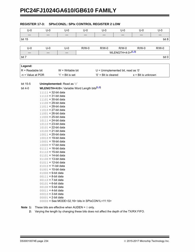
PIC24FJ1024GA610/GB610 FAMILY
REGISTER 17-3: SPIxCON2L: SPIx CONTROL REGISTER 2 LOW
U-0 U-0 U-0 U-0 U-0 U-0 U-0 U-0
— — — — — — — —
bit 15 bit 8
U-0 U-0 U-0 R/W-0 R/W-0 R/W-0 R/W-0 R/W-0
— — — WLENGTH<4:0>(1,2)
bit 7 bit 0
Legend:
R = Readable bit W = Writable bit U = Unimplemented bit, read as ‘0’
-n = Value at POR ‘1’ = Bit is set ‘0’ = Bit is cleared x = Bit is unknown
bit 15-5 Unimplemented: Read as ‘0’
bit 4-0 WLENGTH<4:0>: Variable Word Length bits(1,2)
11111 = 32-bit data11110 = 31-bit data11101 = 30-bit data11100 = 29-bit data11011 = 28-bit data11010 = 27-bit data11001 = 26-bit data11000 = 25-bit data10111 = 24-bit data10110 = 23-bit data10101 = 22-bit data10100 = 21-bit data10011 = 20-bit data10010 = 19-bit data10001 = 18-bit data10000 = 17-bit data01111 = 16-bit data01110 = 15-bit data01101 = 14-bit data01100 = 13-bit data01011 = 12-bit data01010 = 11-bit data01001 = 10-bit data01000 = 9-bit data00111 = 8-bit data00110 = 7-bit data00101 = 6-bit data00100 = 5-bit data00011 = 4-bit data00010 = 3-bit data00001 = 2-bit data00000 = See MODE<32,16> bits in SPIxCON1L<11:10>
Note 1: These bits are effective when AUDEN = 0 only.
2: Varying the length by changing these bits does not affect the depth of the TX/RX FIFO.
DS30010074E-page 234 2015-2017 Microchip Technology Inc.

PIC24FJ1024GA610/GB610 FAMILY
REGISTER 17-4: SPIxSTATL: SPIx STATUS REGISTER LOW
U-0 U-0 U-0 R/C-0, HS R-0, HSC U-0 U-0 R-0, HSC
— — — FRMERR SPIBUSY — — SPITUR(1)
bit 15 bit 8
R-0, HSC R/C-0, HS R-1, HSC U-0 R-1, HSC U-0 R-0, HSC R-0, HSC
SRMT SPIROV SPIRBE — SPITBE — SPITBF SPIRBF
bit 7 bit 0
Legend: C = Clearable bit HS = Hardware Settable bit x = Bit is unknown
R = Readable bit W = Writable bit ‘0’ = Bit is cleared HSC = Hardware Settable/Clearable bit
-n = Value at POR ‘1’ = Bit is set U = Unimplemented bit, read as ‘0’
bit 15-13 Unimplemented: Read as ‘0’
bit 12 FRMERR: SPIx Frame Error Status bit
1 = Frame error is detected0 = No frame error is detected
bit 11 SPIBUSY: SPIx Activity Status bit
1 = Module is currently busy with some transactions0 = No ongoing transactions (at time of read)
bit 10-9 Unimplemented: Read as ‘0’
bit 8 SPITUR: SPIx Transmit Underrun Status bit(1)
1 = Transmit buffer has encountered a Transmit Underrun condition0 = Transmit buffer does not have a Transmit Underrun condition
bit 7 SRMT: Shift Register Empty Status bit
1 = No current or pending transactions (i.e., neither SPIxTXB or SPIxTXSR contains data to transmit)0 = Current or pending transactions
bit 6 SPIROV: SPIx Receive Overflow Status bit
1 = A new byte/half-word/word has been completely received when the SPIxRXB is full0 = No overflow
bit 5 SPIRBE: SPIx RX Buffer Empty Status bit
1 = RX buffer is empty 0 = RX buffer is not empty
Standard Buffer Mode:Automatically set in hardware when SPIxBUF is read from, reading SPIxRXB. Automatically cleared inhardware when SPIx transfers data from SPIxRXSR to SPIxRXB.
Enhanced Buffer Mode:Indicates RXELM<5:0> = 6’b000000.
bit 4 Unimplemented: Read as ‘0’
bit 3 SPITBE: SPIx Transmit Buffer Empty Status bit
1 = SPIxTXB is empty0 = SPIxTXB is not empty
Standard Buffer Mode:Automatically set in hardware when SPIx transfers data from SPIxTXB to SPIxTXSR. Automaticallycleared in hardware when SPIxBUF is written, loading SPIxTXB.
Enhanced Buffer Mode:Indicates TXELM<5:0> = 6’b000000.
Note 1: SPITUR is cleared when SPIEN = 0. When IGNTUR = 1, SPITUR provides dynamic status of the Transmit Underrun condition, but does not stop RX/TX operation and does not need to be cleared by software.
2015-2017 Microchip Technology Inc. DS30010074E-page 235

PIC24FJ1024GA610/GB610 FAMILY
bit 2 Unimplemented: Read as ‘0’
bit 1 SPITBF: SPIx Transmit Buffer Full Status bit
1 = SPIxTXB is full0 = SPIxTXB not full
Standard Buffer Mode:Automatically set in hardware when SPIxBUF is written, loading SPIxTXB. Automatically cleared inhardware when SPIx transfers data from SPIxTXB to SPIxTXSR.
Enhanced Buffer Mode:Indicates TXELM<5:0> = 6’b111111.
bit 0 SPIRBF: SPIx Receive Buffer Full Status bit
1 = SPIxRXB is full0 = SPIxRXB is not full
Standard Buffer Mode:Automatically set in hardware when SPIx transfers data from SPIxRXSR to SPIxRXB. Automaticallycleared in hardware when SPIxBUF is read from, reading SPIxRXB.
Enhanced Buffer Mode:Indicates RXELM<5:0> = 6’b111111.
REGISTER 17-4: SPIxSTATL: SPIx STATUS REGISTER LOW (CONTINUED)
Note 1: SPITUR is cleared when SPIEN = 0. When IGNTUR = 1, SPITUR provides dynamic status of the Transmit Underrun condition, but does not stop RX/TX operation and does not need to be cleared by software.
DS30010074E-page 236 2015-2017 Microchip Technology Inc.

PIC24FJ1024GA610/GB610 FAMILY
REGISTER 17-5: SPIxSTATH: SPIx STATUS REGISTER HIGH
U-0 U-0 R-0, HSC R-0, HSC R-0, HSC R-0, HSC R-0, HSC R-0, HSC
— — RXELM5(3) RXELM4(2) RXELM3(1) RXELM2 RXELM1 RXELM0
bit 15 bit 8
U-0 U-0 R-0, HSC R-0, HSC R-0, HSC R-0, HSC R-0, HSC R-0, HSC
— — TXELM5(3) TXELM4(2) TXELM3(1) TXELM2 TXELM1 TXELM0
bit 7 bit 0
Legend: HSC = Hardware Settable/Clearable bit
R = Readable bit W = Writable bit U = Unimplemented bit, read as ‘0’
-n = Value at POR ‘1’ = Bit is set ‘0’ = Bit is cleared x = Bit is unknown
bit 15-14 Unimplemented: Read as ‘0’
bit 13-8 RXELM<5:0>: Receive Buffer Element Count bits (valid in Enhanced Buffer mode)(1,2,3)
bit 7-6 Unimplemented: Read as ‘0’
bit 5-0 TXELM<5:0>: Transmit Buffer Element Count bits (valid in Enhanced Buffer mode)(1,2,3)
Note 1: RXELM3 and TXELM3 bits are only present when FIFODEPTH = 8 or higher.
2: RXELM4 and TXELM4 bits are only present when FIFODEPTH = 16 or higher.
3: RXELM5 and TXELM5 bits are only present when FIFODEPTH = 32.
2015-2017 Microchip Technology Inc. DS30010074E-page 237

PIC24FJ1024GA610/GB610 FAMILY
REGISTER 17-6: SPIxBUFL: SPIx BUFFER REGISTER LOW
R/W-0 R/W-0 R/W-0 R/W-0 R/W-0 R/W-0 R/W-0 R/W-0
DATA<15:8>
bit 15 bit 8
R/W-0 R/W-0 R/W-0 R/W-0 R/W-0 R/W-0 R/W-0 R/W-0
DATA<7:0>
bit 7 bit 0
Legend:
R = Readable bit W = Writable bit U = Unimplemented bit, read as ‘0’
-n = Value at POR ‘1’ = Bit is set ‘0’ = Bit is cleared x = Bit is unknown
bit 15-0 DATA<15:0>: SPIx FIFO Data bits
When the MODE<32,16> or WLENGTH<4:0> bits select 16 to 9-bit data, the SPIx only usesDATA<15:0>. When the MODE<32,16> or WLENGTH<4:0> bits select 8 to 2-bit data, the SPIx only usesDATA<7:0>.
REGISTER 17-7: SPIxBUFH: SPIx BUFFER REGISTER HIGH
R/W-0 R/W-0 R/W-0 R/W-0 R/W-0 R/W-0 R/W-0 R/W-0
DATA<31:24>
bit 15 bit 8
R/W-0 R/W-0 R/W-0 R/W-0 R/W-0 R/W-0 R/W-0 R/W-0
DATA<23:16>
bit 7 bit 0
Legend:
R = Readable bit W = Writable bit U = Unimplemented bit, read as ‘0’
-n = Value at POR ‘1’ = Bit is set ‘0’ = Bit is cleared x = Bit is unknown
bit 15-0 DATA<31:16>: SPIx FIFO Data bits
When the MODE<32,16> or WLENGTH<4:0> bits select 32 to 25-bit data, the SPIx uses DATA<31:16>.When the MODE<32,16> or WLENGTH<4:0> bits select 24 to 17-bit data, the SPIx only usesDATA<23:16>.
DS30010074E-page 238 2015-2017 Microchip Technology Inc.
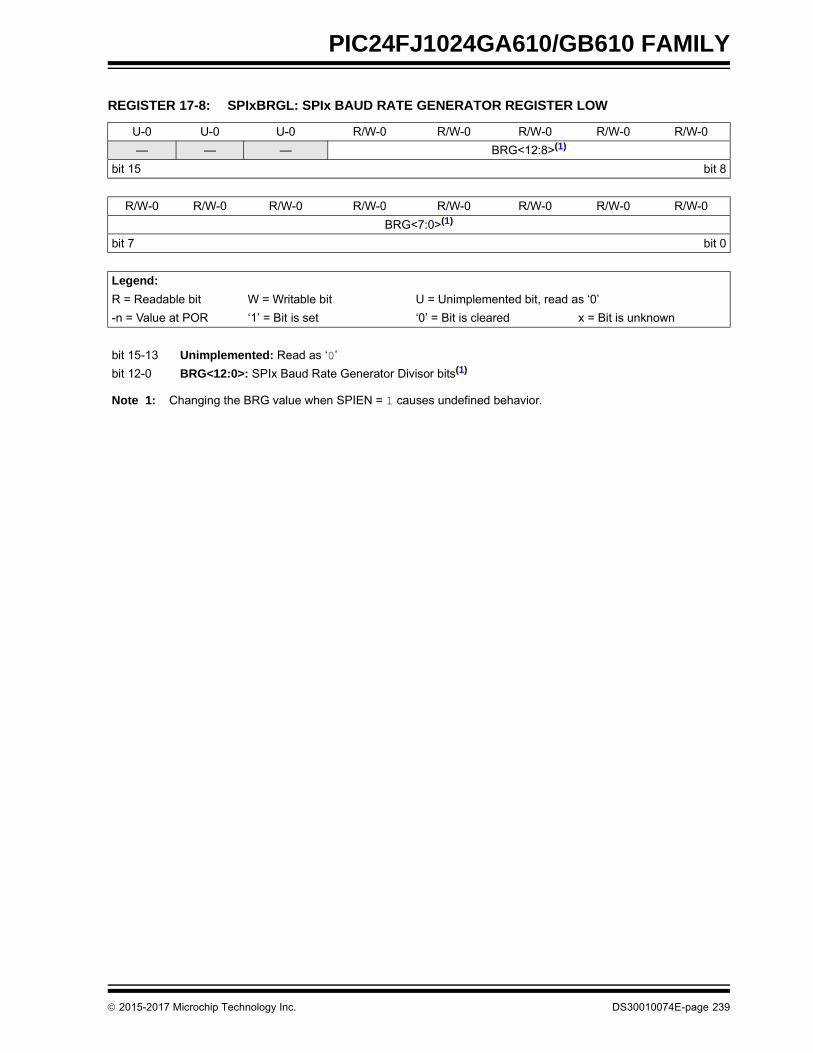
PIC24FJ1024GA610/GB610 FAMILY
REGISTER 17-8: SPIxBRGL: SPIx BAUD RATE GENERATOR REGISTER LOW
U-0 U-0 U-0 R/W-0 R/W-0 R/W-0 R/W-0 R/W-0
— — — BRG<12:8>(1)
bit 15 bit 8
R/W-0 R/W-0 R/W-0 R/W-0 R/W-0 R/W-0 R/W-0 R/W-0
BRG<7:0>(1)
bit 7 bit 0
Legend:
R = Readable bit W = Writable bit U = Unimplemented bit, read as ‘0’
-n = Value at POR ‘1’ = Bit is set ‘0’ = Bit is cleared x = Bit is unknown
bit 15-13 Unimplemented: Read as ‘0’
bit 12-0 BRG<12:0>: SPIx Baud Rate Generator Divisor bits(1)
Note 1: Changing the BRG value when SPIEN = 1 causes undefined behavior.
2015-2017 Microchip Technology Inc. DS30010074E-page 239

PIC24FJ1024GA610/GB610 FAMILY
REGISTER 17-9: SPIxIMSKL: SPIx INTERRUPT MASK REGISTER LOW
U-0 U-0 U-0 R/W-0 R/W-0 U-0 U-0 R/W-0
— — — FRMERREN BUSYEN — — SPITUREN
bit 15 bit 8
R/W-0 R/W-0 R/W-0 U-0 R/W-0 U-0 R/W-0 R/W-0
SRMTEN SPIROVEN SPIRBEN — SPITBEN — SPITBFEN SPIRBFEN
bit 7 bit 0
Legend:
R = Readable bit W = Writable bit U = Unimplemented bit, read as ‘0’
-n = Value at POR ‘1’ = Bit is set ‘0’ = Bit is cleared x = Bit is unknown
bit 15-13 Unimplemented: Read as ‘0’
bit 12 FRMERREN: Enable Interrupt Events via FRMERR bit
1 = Frame error generates an interrupt event0 = Frame error does not generate an interrupt event
bit 11 BUSYEN: Enable Interrupt Events via SPIBUSY bit
1 = SPIBUSY generates an interrupt event0 = SPIBUSY does not generate an interrupt event
bit 10-9 Unimplemented: Read as ‘0’
bit 8 SPITUREN: Enable Interrupt Events via SPITUR bit
1 = Transmit Underrun (TUR) generates an interrupt event0 = Transmit Underrun does not generate an interrupt event
bit 7 SRMTEN: Enable Interrupt Events via SRMT bit
1 = Shift Register Empty (SRMT) generates interrupt events0 = Shift Register Empty does not generate interrupt events
bit 6 SPIROVEN: Enable Interrupt Events via SPIROV bit
1 = SPIx Receive Overflow generates an interrupt event0 = SPIx Receive Overflow does not generate an interrupt event
bit 5 SPIRBEN: Enable Interrupt Events via SPIRBE bit
1 = SPIx RX Buffer Empty generates an interrupt event0 = SPIx RX Buffer Empty does not generate an interrupt event
bit 4 Unimplemented: Read as ‘0’
bit 3 SPITBEN: Enable Interrupt Events via SPITBE bit
1 = SPIx Transmit Buffer Empty generates an interrupt event0 = SPIx Transmit Buffer Empty does not generate an interrupt event
bit 2 Unimplemented: Read as ‘0’
bit 1 SPITBFEN: Enable Interrupt Events via SPITBF bit
1 = SPIx Transmit Buffer Full generates an interrupt event0 = SPIx Transmit Buffer Full does not generate an interrupt event
bit 0 SPIRBFEN: Enable Interrupt Events via SPIRBF bit
1 = SPIx Receive Buffer Full generates an interrupt event0 = SPIx Receive Buffer Full does not generate an interrupt event
DS30010074E-page 240 2015-2017 Microchip Technology Inc.

PIC24FJ1024GA610/GB610 FAMILY
REGISTER 17-10: SPIxIMSKH: SPIx INTERRUPT MASK REGISTER HIGH
R/W-0 U-0 R/W-0 R/W-0 R/W-0 R/W-0 R/W-0 R/W-0
RXWIEN — RXMSK5(1) RXMSK4(1,4) RXMSK3(1,3) RXMSK2(1,2) RXMSK1(1) RXMSK0(1)
bit 15 bit 8
R/W-0 U-0 R/W-0 R/W-0 R/W-0 R/W-0 R/W-0 R/W-0
TXWIEN — TXMSK5(1) TXMSK4(1,4) TXMSK3(1,3) TXMSK2(1,2) TXMSK1(1) TXMSK0(1)
bit 7 bit 0
Legend:
R = Readable bit W = Writable bit U = Unimplemented bit, read as ‘0’
-n = Value at POR ‘1’ = Bit is set ‘0’ = Bit is cleared x = Bit is unknown
bit 15 RXWIEN: Receive Watermark Interrupt Enable bit
1 = Triggers receive buffer element watermark interrupt when RXMSK<5:0> RXELM<5:0>0 = Disables receive buffer element watermark interrupt
bit 14 Unimplemented: Read as ‘0’
bit 13-8 RXMSK<5:0>: RX Buffer Mask bits(1,2,3,4)
RX mask bits; used in conjunction with the RXWIEN bit.
bit 7 TXWIEN: Transmit Watermark Interrupt Enable bit
1 = Triggers transmit buffer element watermark interrupt when TXMSK<5:0> = TXELM<5:0>0 = Disables transmit buffer element watermark interrupt
bit 6 Unimplemented: Read as ‘0’
bit 5-0 TXMSK<5:0>: TX Buffer Mask bits(1,2,3,4)
TX mask bits; used in conjunction with the TXWIEN bit.
Note 1: Mask values higher than FIFODEPTH are not valid. The module will not trigger a match for any value in this case.
2: RXMSK2 and TXMSK2 bits are only present when FIFODEPTH = 8 or higher.
3: RXMSK3 and TXMSK3 bits are only present when FIFODEPTH = 16 or higher.
4: RXMSK4 and TXMSK4 bits are only present when FIFODEPTH = 32.
2015-2017 Microchip Technology Inc. DS30010074E-page 241

PIC24FJ1024GA610/GB610 FAMILY
REGISTER 17-11: SPIxURDTL: SPIx UNDERRUN DATA REGISTER LOW
R/W-0 R/W-0 R/W-0 R/W-0 R/W-0 R/W-0 R/W-0 R/W-0
URDATA<15:8>
bit 15 bit 8
R/W-0 R/W-0 R/W-0 R/W-0 R/W-0 R/W-0 R/W-0 R/W-0
URDATA<7:0>
bit 7 bit 0
Legend:
R = Readable bit W = Writable bit U = Unimplemented bit, read as ‘0’
-n = Value at POR ‘1’ = Bit is set ‘0’ = Bit is cleared x = Bit is unknown
bit 15-0 URDATA<15:0>: SPIx Underrun Data bits
These bits are only used when URDTEN = 1. This register holds the data to transmit when a TransmitUnderrun condition occurs.
When the MODE<32,16> or WLENGTH<4:0> bits select 16 to 9-bit data, the SPIx only usesURDATA<15:0>. When the MODE<32,16> or WLENGTH<4:0> bits select 8 to 2-bit data, the SPIx onlyuses URDATA<7:0>.
REGISTER 17-12: SPIxURDTH: SPIx UNDERRUN DATA REGISTER HIGH
R/W-0 R/W-0 R/W-0 R/W-0 R/W-0 R/W-0 R/W-0 R/W-0
URDATA<31:24>
bit 15 bit 8
R/W-0 R/W-0 R/W-0 R/W-0 R/W-0 R/W-0 R/W-0 R/W-0
URDATA<23:16>
bit 7 bit 0
Legend:
R = Readable bit W = Writable bit U = Unimplemented bit, read as ‘0’
-n = Value at POR ‘1’ = Bit is set ‘0’ = Bit is cleared x = Bit is unknown
bit 15-0 URDATA<31:16>: SPIx Underrun Data bits
These bits are only used when URDTEN = 1. This register holds the data to transmit when a TransmitUnderrun condition occurs.
When the MODE<32,16> or WLENGTH<4:0> bits select 32 to 25-bit data, the SPIx only usesURDATA<15:0>. When the MODE<32,16> or WLENGTH<4:0> bits select 24 to 17-bit data, the SPIx onlyuses URDATA<7:0>.
DS30010074E-page 242 2015-2017 Microchip Technology Inc.

PIC24FJ1024GA610/GB610 FAMILY
FIGURE 17-2: SPIx MASTER/SLAVE CONNECTION (STANDARD MODE)
Serial Transmit Buffer(SPIxTXB)(2)
Shift Register(SPIxTXSR)
LSbMSb
SDIx
SDOx
Processor 2 (SPIx Slave)
SCKx
SSx(1)
Serial Receive Buffer(SPIxRXB)(2)
Serial Receive Buffer(SPIxRXB)(2)
Shift Register(SPIxRXSR)
MSb LSb
SDOx
SDIx
Processor 1 (SPIx Master)
Serial Clock
MSSEN (SPIxCON1H<4>) = 1 and MSTEN (SPIxCON1L<5>) = 0
Note 1: Using the SSx pin in Slave mode of operation is optional.
2: User must write transmit data to read the received data from SPIxBUF. The SPIxTXB and SPIxRXB registers are memory-mapped to SPIxBUF.
SCKxSerial Transmit Buffer(SPIxTXB)(2)
MSTEN (SPIxCON1L<5>) = 1
SPIx Buffer(SPIxBUF)
SPIx Buffer(SPIxBUF)
Shift Register(SPIxTXSR)
Shift Register(SPIxRXSR)
MSb LSb LSbMSb
SDOx SDIx
2015-2017 Microchip Technology Inc. DS30010074E-page 243

PIC24FJ1024GA610/GB610 FAMILY
FIGURE 17-3: SPIx MASTER/SLAVE CONNECTION (ENHANCED BUFFER MODES)
Serial Transmit FIFO(SPIxTXB)(2)
Shift Register(SPIxTXSR)
LSbMSb
SDIx
SDOx
Processor 2 (SPIx Slave)
SCKx
SSx(1)
Serial Receive FIFO(SPIxRXB)(2)
Serial Receive FIFO(SPIxRXB)(2)
Shift Register(SPIxRXSR)
MSb LSb
SDOx
SDIx
Processor 1 (SPIx Master)
Serial Clock
MSSEN (SPIxCON1H<4>) = 1 and MSTEN (SPIxCON1L<5>) = 0
SCKxSerial Transmit FIFO(SPIxTXB)(2)
MSTEN (SPIxCON1L<5>) = 1
SPIx Buffer(SPIxBUF)
SPIx Buffer(SPIxBUF)
Shift Register(SPIxTXSR)
Shift Register(SPIxRXSR)
MSb LSb LSbMSb
SDOx SDIx
Note 1: Using the SSx pin in Slave mode of operation is optional.
2: User must write transmit data to read the received data from SPIxBUF. The SPIxTXB and SPIxRXB registers are memory-mapped to SPIxBUF.
DS30010074E-page 244 2015-2017 Microchip Technology Inc.

PIC24FJ1024GA610/GB610 FAMILY
FIGURE 17-4: SPIx MASTER, FRAME MASTER CONNECTION DIAGRAM
PIC24FJ1024GA610/GB610
Serial ClockSCKx
Frame SyncPulse(1,2)
SDIx
SDOx
Processor 2
SSx
SCKx
(SPIx Master, Frame Master)
Serial Receive Buffer(SPIxRXB)(3)
Shift Register(SPIxRXSR)
Shift Register(SPIxTXSR)
Serial Transmit Buffer(SPIxTXB)(3)
(SPIxBUF)SPI Buffer
Serial Receive Buffer(SPIxTXB)(3)
Shift Register(SPIxRXSR)
Shift Register(SPIxTXSR)
Serial Transmit Buffer(SPIxTXB)(3)
(SPIxBUF)SPI Buffer
(SPIx Slave, Frame Slave)
SSx(1)
SDOx
SDIxMSb LSb
MSb LSb
MSb LSb
MSb LSb
Note 1: In Framed SPI modes, the SSx pin is used to transmit/receive the Frame Synchronization pulse.2: Framed SPI modes require the use of all four pins (i.e., using the SSx pin is not optional).3: The SPIxTXB and SPIxRXB registers are memory-mapped to the SPIxBUF register.
2015-2017 Microchip Technology Inc. DS30010074E-page 245

PIC24FJ1024GA610/GB610 FAMILY
FIGURE 17-5: SPIx MASTER, FRAME SLAVE CONNECTION DIAGRAM
FIGURE 17-6: SPIx SLAVE, FRAME MASTER CONNECTION DIAGRAM
FIGURE 17-7: SPIx SLAVE, FRAME SLAVE CONNECTION DIAGRAM
EQUATION 17-1: RELATIONSHIP BETWEEN DEVICE AND SPIx CLOCK SPEED
SDOx
SDIx
PIC24F
Serial Clock
SSx
SCKx
Frame SyncPulse
SDIx
SDOx
Processor 2
SSx
SCKx
SPIx Master, Frame Slave)
SDOx
SDIx
PIC24F
Serial Clock
SSx
SCKx
Frame Sync.Pulse
SDIx
SDOx
Processor 2
SSx
SCKx
(SPIx Slave, Frame Master)
SDOx
SDIx
PIC24F
Serial Clock
SSx
SCKx
Frame SyncPulse
SDIx
SDOx
Processor 2
SSx
SCKx
(SPIx Slave, Frame Slave)
Baud Rate =FPB
(2 * (SPIxBRG + 1))
Where:
FPB is the Peripheral Bus Clock Frequency.
DS30010074E-page 246 2015-2017 Microchip Technology Inc.

PIC24FJ1024GA610/GB610 FAMILY
18.0 INTER-INTEGRATED CIRCUIT (I2C)
The Inter-Integrated Circuit (I2C) module is a serialinterface useful for communicating with other periph-eral or microcontroller devices. These peripheraldevices may be serial EEPROMs, display drivers, A/DConverters, etc.
The I2C module supports these features:
• Independent Master and Slave Logic
• 7-Bit and 10-Bit Device Addresses
• General Call Address as Defined in the I2C Protocol
• Clock Stretching to Provide Delays for the Processor to Respond to a Slave Data Request
• Both 100 kHz and 400 kHz Bus Specifications
• Configurable Address Masking
• Multi-Master modes to Prevent Loss of Messages in Arbitration
• Bus Repeater mode, Allowing the Acceptance of All Messages as a Slave, Regardless of the Address
• Automatic SCL
A block diagram of the module is shown in Figure 18-1.
18.1 Communicating as a Master in a Single Master Environment
The details of sending a message in Master modedepends on the communications protocol for the devicebeing communicated with. Typically, the sequence ofevents is as follows:
1. Assert a Start condition on SDAx and SCLx.
2. Send the I2C device address byte to the slavewith a write indication.
3. Wait for and verify an Acknowledge from theslave.
4. Send the first data byte (sometimes known asthe command) to the slave.
5. Wait for and verify an Acknowledge from theslave.
6. Send the serial memory address low byte to theslave.
7. Repeat Steps 4 and 5 until all data bytes aresent.
8. Assert a Repeated Start condition on SDAx andSCLx.
9. Send the device address byte to the slave witha read indication.
10. Wait for and verify an Acknowledge from theslave.
11. Enable master reception to receive serialmemory data.
12. Generate an ACK or NACK condition at the endof a received byte of data.
13. Generate a Stop condition on SDAx and SCLx.
Note: This data sheet summarizes the featuresof this group of PIC24F devices. It is notintended to be a comprehensive refer-ence source. For more information, referto the “dsPIC33/PIC24 Family ReferenceManual”, “Inter-Integrated Circuit (I2C)”(DS70000195), which is available from theMicrochip web site (www.microchip.com).The information in this data sheetsupersedes the information in the FRM.
2015-2017 Microchip Technology Inc. DS30010074E-page 247

PIC24FJ1024GA610/GB610 FAMILY
FIGURE 18-1: I2Cx BLOCK DIAGRAM
I2CxRCV
InternalData Bus
SCLx
SDAx
Shift
Match Detect
Start and StopBit Detect
Clock
Address Match
ClockStretching
I2CxTRN
LSBShift Clock
BRG Down Counter
ReloadControl
TCY/2
Start and StopBit Generation
AcknowledgeGeneration
CollisionDetect
I2CxCON
I2CxSTAT
Co
ntr
ol L
og
ic
Read
LSB
Write
Read
I2CxBRG
I2CxRSR
Write
Read
Write
Read
Write
Read
Write
Read
Write
Read
I2CxMSK
I2CxADD
DS30010074E-page 248 2015-2017 Microchip Technology Inc.

PIC24FJ1024GA610/GB610 FAMILY
18.2 Setting Baud Rate When Operating as a Bus Master
To compute the Baud Rate Generator reload value, useEquation 18-1.
EQUATION 18-1: COMPUTING BAUD RATE RELOAD VALUE(1,2,3)
18.3 Slave Address Masking
The I2CxMSK register (Register 18-4) designatesaddress bit positions as “don’t care” for both 7-Bit and10-Bit Addressing modes. Setting a particular bitlocation (= 1) in the I2CxMSK register causes the slavemodule to respond, whether the corresponding addressbit value is a ‘0’ or a ‘1’. For example, when I2CxMSK isset to ‘0010000000’, the slave module will detect bothaddresses, ‘0000000000’ and ‘0010000000’.
To enable address masking, the Intelligent PeripheralManagement Interface (IPMI) must be disabled byclearing the STRICT bit (I2CxCONL<11>).
TABLE 18-2: I2Cx RESERVED ADDRESSES(1)
Note 1: Based on FCY = FOSC/2; Doze mode and PLL are disabled.
2: These clock rate values are for guidance only. The actual clock rate can be affected by various system-level parameters. The actual clock rate should be measured in its intended application.
3: BRG values of 0 and 1 are forbidden.
FSCL =FCY
(I2CxBRG + 2) * 2
[ FCY(FSCL * 2)
– 2
or:
]I2CxBRG =
Note: As a result of changes in the I2C protocol,the addresses in Table 18-2 are reservedand will not be Acknowledged in Slavemode. This includes any address masksettings that include any of theseaddresses.
TABLE 18-1: I2Cx CLOCK RATES(1,2)
Required System FSCL FCYI2CxBRG Value
Actual FSCL(Decimal) (Hexadecimal)
100 kHz 16 MHz 78 4E 100 kHz
100 kHz 8 MHz 38 26 100 kHz
100 kHz 4 MHz 18 12 100 kHz
400 kHz 16 MHz 18 12 400 kHz
400 kHz 8 MHz 8 8 400 kHz
400 kHz 4 MHz 3 3 400 kHz
1 MHz 16 MHz 6 6 1.000 MHz
1 MHz 8 MHz 2 2 1.000 MHz
Note 1: Based on FCY = FOSC/2; Doze mode and PLL are disabled.2: These clock rate values are for guidance only. The actual clock rate can be affected by various
system-level parameters. The actual clock rate should be measured in its intended application.
Slave Address R/W Bit Description
0000 000 0 General Call Address(2)
0000 000 1 Start Byte
0000 001 x CBus Address
0000 01x x Reserved
0000 1xx x HS Mode Master Code
1111 0xx x 10-Bit Slave Upper Byte(3)
1111 1xx x Reserved
Note 1: The address bits listed here will never cause an address match independent of address mask settings.2: This address will be Acknowledged only if GCEN = 1.3: A match on this address can only occur on the upper byte in 10-Bit Addressing mode.
2015-2017 Microchip Technology Inc. DS30010074E-page 249
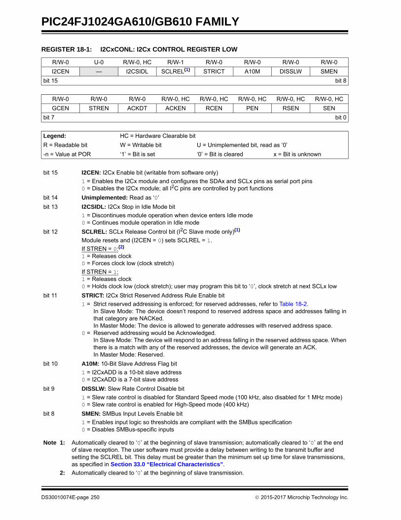
PIC24FJ1024GA610/GB610 FAMILY
REGISTER 18-1: I2CxCONL: I2Cx CONTROL REGISTER LOW
R/W-0 U-0 R/W-0, HC R/W-1 R/W-0 R/W-0 R/W-0 R/W-0
I2CEN — I2CSIDL SCLREL(1) STRICT A10M DISSLW SMEN
bit 15 bit 8
R/W-0 R/W-0 R/W-0 R/W-0, HC R/W-0, HC R/W-0, HC R/W-0, HC R/W-0, HC
GCEN STREN ACKDT ACKEN RCEN PEN RSEN SEN
bit 7 bit 0
Legend: HC = Hardware Clearable bit
R = Readable bit W = Writable bit U = Unimplemented bit, read as ‘0’
-n = Value at POR ‘1’ = Bit is set ‘0’ = Bit is cleared x = Bit is unknown
bit 15 I2CEN: I2Cx Enable bit (writable from software only)
1 = Enables the I2Cx module and configures the SDAx and SCLx pins as serial port pins0 = Disables the I2Cx module; all I2C pins are controlled by port functions
bit 14 Unimplemented: Read as ‘0’
bit 13 I2CSIDL: I2Cx Stop in Idle Mode bit
1 = Discontinues module operation when device enters Idle mode0 = Continues module operation in Idle mode
bit 12 SCLREL: SCLx Release Control bit (I2C Slave mode only)(1)
Module resets and (I2CEN = 0) sets SCLREL = 1.
If STREN = 0:(2)
1 = Releases clock0 = Forces clock low (clock stretch)
If STREN = 1:1 = Releases clock0 = Holds clock low (clock stretch); user may program this bit to ‘0’, clock stretch at next SCLx low
bit 11 STRICT: I2Cx Strict Reserved Address Rule Enable bit
1 = Strict reserved addressing is enforced; for reserved addresses, refer to Table 18-2. In Slave Mode: The device doesn’t respond to reserved address space and addresses falling inthat category are NACKed.In Master Mode: The device is allowed to generate addresses with reserved address space.
0 = Reserved addressing would be Acknowledged.In Slave Mode: The device will respond to an address falling in the reserved address space. Whenthere is a match with any of the reserved addresses, the device will generate an ACK.In Master Mode: Reserved.
bit 10 A10M: 10-Bit Slave Address Flag bit
1 = I2CxADD is a 10-bit slave address0 = I2CxADD is a 7-bit slave address
bit 9 DISSLW: Slew Rate Control Disable bit
1 = Slew rate control is disabled for Standard Speed mode (100 kHz, also disabled for 1 MHz mode)0 = Slew rate control is enabled for High-Speed mode (400 kHz)
bit 8 SMEN: SMBus Input Levels Enable bit
1 = Enables input logic so thresholds are compliant with the SMBus specification0 = Disables SMBus-specific inputs
Note 1: Automatically cleared to ‘0’ at the beginning of slave transmission; automatically cleared to ‘0’ at the end of slave reception. The user software must provide a delay between writing to the transmit buffer and setting the SCLREL bit. This delay must be greater than the minimum set up time for slave transmissions, as specified in Section 33.0 “Electrical Characteristics”.
2: Automatically cleared to ‘0’ at the beginning of slave transmission.
DS30010074E-page 250 2015-2017 Microchip Technology Inc.

PIC24FJ1024GA610/GB610 FAMILY
bit 7 GCEN: General Call Enable bit (I2C Slave mode only)
1 = Enables interrupt when a general call address is received in I2CxRSR; module is enabled for reception0 = General call address is disabled.
bit 6 STREN: SCLx Clock Stretch Enable bit
In I2C Slave mode only; used in conjunction with the SCLREL bit.1 = Enables clock stretching0 = Disables clock stretching
bit 5 ACKDT: Acknowledge Data bit
In I2C Master mode during Master Receive mode. The value that will be transmitted when the userinitiates an Acknowledge sequence at the end of a receive.In I2C Slave mode when AHEN = 1 or DHEN = 1. The value that the slave will transmit when it initiatesan Acknowledge sequence at the end of an address or data reception.1 = NACK is sent0 = ACK is sent
bit 4 ACKEN: Acknowledge Sequence Enable bit
In I2C Master mode only; applicable during Master Receive mode.1 = Initiates Acknowledge sequence on SDAx and SCLx pins, and transmits ACKDT data bit0 = Acknowledge sequence is Idle
bit 3 RCEN: Receive Enable bit (I2C Master mode only)
1 = Enables Receive mode for I2C; automatically cleared by hardware at end of 8-bit receive data byte0 = Receive sequence is not in progress
bit 2 PEN: Stop Condition Enable bit (I2C Master mode only)
1 = Initiates Stop condition on SDAx and SCLx pins0 = Stop condition is Idle
bit 1 RSEN: Restart Condition Enable bit (I2C Master mode only)
1 = Initiates Restart condition on SDAx and SCLx pins0 = Restart condition is Idle
bit 0 SEN: Start Condition Enable bit (I2C Master mode only)
1 = Initiates Start condition on SDAx and SCLx pins0 = Start condition is Idle
REGISTER 18-1: I2CxCONL: I2Cx CONTROL REGISTER LOW (CONTINUED)
Note 1: Automatically cleared to ‘0’ at the beginning of slave transmission; automatically cleared to ‘0’ at the end of slave reception. The user software must provide a delay between writing to the transmit buffer and setting the SCLREL bit. This delay must be greater than the minimum set up time for slave transmissions, as specified in Section 33.0 “Electrical Characteristics”.
2: Automatically cleared to ‘0’ at the beginning of slave transmission.
2015-2017 Microchip Technology Inc. DS30010074E-page 251
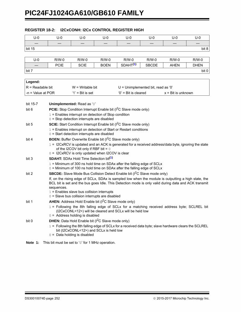
PIC24FJ1024GA610/GB610 FAMILY
REGISTER 18-2: I2CxCONH: I2Cx CONTROL REGISTER HIGH
U-0 U-0 U-0 U-0 U-0 U-0 U-0 U-0
— — — — — — — —
bit 15 bit 8
U-0 R/W-0 R/W-0 R/W-0 R/W-0 R/W-0 R/W-0 R/W-0
— PCIE SCIE BOEN SDAHT(1) SBCDE AHEN DHEN
bit 7 bit 0
Legend:
R = Readable bit W = Writable bit U = Unimplemented bit, read as ‘0’
-n = Value at POR ‘1’ = Bit is set ‘0’ = Bit is cleared x = Bit is unknown
bit 15-7 Unimplemented: Read as ‘0’
bit 6 PCIE: Stop Condition Interrupt Enable bit (I2C Slave mode only)
1 = Enables interrupt on detection of Stop condition0 = Stop detection interrupts are disabled
bit 5 SCIE: Start Condition Interrupt Enable bit (I2C Slave mode only)
1 = Enables interrupt on detection of Start or Restart conditions0 = Start detection interrupts are disabled
bit 4 BOEN: Buffer Overwrite Enable bit (I2C Slave mode only)
1 = I2CxRCV is updated and an ACK is generated for a received address/data byte, ignoring the stateof the I2COV bit only if RBF bit = 0
0 = I2CxRCV is only updated when I2COV is clear
bit 3 SDAHT: SDAx Hold Time Selection bit(1)
1 = Minimum of 300 ns hold time on SDAx after the falling edge of SCLx0 = Minimum of 100 ns hold time on SDAx after the falling edge of SCLx
bit 2 SBCDE: Slave Mode Bus Collision Detect Enable bit (I2C Slave mode only)
If, on the rising edge of SCLx, SDAx is sampled low when the module is outputting a high state, theBCL bit is set and the bus goes Idle. This Detection mode is only valid during data and ACK transmitsequences.1 = Enables slave bus collision interrupts0 = Slave bus collision interrupts are disabled
bit 1 AHEN: Address Hold Enable bit (I2C Slave mode only)
1 = Following the 8th falling edge of SCLx for a matching received address byte; SCLREL bit(I2CxCONL<12>) will be cleared and SCLx will be held low
0 = Address holding is disabled
bit 0 DHEN: Data Hold Enable bit (I2C Slave mode only)
1 = Following the 8th falling edge of SCLx for a received data byte; slave hardware clears the SCLRELbit (I2CxCONL<12>) and SCLx is held low
0 = Data holding is disabled
Note 1: This bit must be set to ‘0’ for 1 MHz operation.
DS30010074E-page 252 2015-2017 Microchip Technology Inc.

PIC24FJ1024GA610/GB610 FAMILY
REGISTER 18-3: I2CxSTAT: I2Cx STATUS REGISTER
R-0, HSC R-0, HSC R-0, HSC U-0 U-0 R/C-0, HSC R-0, HSC R-0, HSC
ACKSTAT TRSTAT ACKTIM — — BCL GCSTAT ADD10
bit 15 bit 8
R/C-0, HS R/C-0, HS R-0, HSC R/C-0, HSC R/C-0, HSC R-0, HSC R-0, HSC R-0, HSC
IWCOL I2COV D/A P S R/W RBF TBF
bit 7 bit 0
Legend: C = Clearable bit HS = Hardware Settable bit
R = Readable bit W = Writable bit U = Unimplemented bit, read as ‘0’
-n = Value at POR ‘1’ = Bit is set ‘0’ = Bit is cleared x = Bit is unknown
HSC = Hardware Settable/Clearable bit
bit 15 ACKSTAT: Acknowledge Status bit (updated in all Master and Slave modes)
1 = Acknowledge was not received from slave0 = Acknowledge was received from slave
bit 14 TRSTAT: Transmit Status bit (when operating as I2C master; applicable to master transmit operation)
1 = Master transmit is in progress (8 bits + ACK)0 = Master transmit is not in progress
bit 13 ACKTIM: Acknowledge Time Status bit (valid in I2C Slave mode only)
1 = Indicates I2C bus is in an Acknowledge sequence, set on 8th falling edge of SCLx clock0 = Not an Acknowledge sequence, cleared on 9th rising edge of SCLx clock
bit 12-11 Unimplemented: Read as ‘0’
bit 10 BCL: Bus Collision Detect bit (Master/Slave mode; cleared when I2C module is disabled, I2CEN = 0)
1 = A bus collision has been detected during a master or slave transmit operation0 = No bus collision has been detected
bit 9 GCSTAT: General Call Status bit (cleared after Stop detection)
1 = General call address was received0 = General call address was not received
bit 8 ADD10: 10-Bit Address Status bit (cleared after Stop detection)
1 = 10-bit address was matched0 = 10-bit address was not matched
bit 7 IWCOL: I2Cx Write Collision Detect bit
1 = An attempt to write to the I2CxTRN register failed because the I2C module is busy; must be clearedin software
0 = No collision
bit 6 I2COV: I2Cx Receive Overflow Flag bit
1 = A byte was received while the I2CxRCV register is still holding the previous byte; I2COV is a “don’tcare” in Transmit mode, must be cleared in software
0 = No overflow
bit 5 D/A: Data/Address bit (when operating as I2C slave)
1 = Indicates that the last byte received was data0 = Indicates that the last byte received or transmitted was an address
bit 4 P: I2Cx Stop bit
Updated when Start, Reset or Stop is detected; cleared when the I2C module is disabled, I2CEN = 0.1 = Indicates that a Stop bit has been detected last0 = Stop bit was not detected last
2015-2017 Microchip Technology Inc. DS30010074E-page 253

PIC24FJ1024GA610/GB610 FAMILY
bit 3 S: I2Cx Start bit
Updated when Start, Reset or Stop is detected; cleared when the I2C module is disabled, I2CEN = 0.1 = Indicates that a Start (or Repeated Start) bit has been detected last0 = Start (or Repeated Start) bit was not detected last
bit 2 R/W: Read/Write Information bit (when operating as I2C slave)
1 = Read: Indicates the data transfer is output from the slave0 = Write: Indicates the data transfer is input to the slave
bit 1 RBF: Receive Buffer Full Status bit
1 = Receive is complete, I2CxRCV is full0 = Receive is not complete, I2CxRCV is empty
bit 0 TBF: Transmit Buffer Full Status bit
1 = Transmit is in progress, I2CxTRN is full (8-bits of data)0 = Transmit is complete, I2CxTRN is empty
REGISTER 18-3: I2CxSTAT: I2Cx STATUS REGISTER (CONTINUED)
REGISTER 18-4: I2CxMSK: I2Cx SLAVE MODE ADDRESS MASK REGISTER
U-0 U-0 U-0 U-0 U-0 U-0 R/W-0 R/W-0
— — — — — — MSK<9:8>
bit 15 bit 8
R/W-0 R/W-0 R/W-0 R/W-0 R/W-0 R/W-0 R/W-0 R/W-0
MSK<7:0>
bit 7 bit 0
Legend:
R = Readable bit W = Writable bit U = Unimplemented bit, read as ‘0’
-n = Value at POR ‘1’ = Bit is set ‘0’ = Bit is cleared x = Bit is unknown
bit 15-10 Unimplemented: Read as ‘0’
bit 9-0 MSK<9:0>: I2Cx Mask for Address Bit x Select bits
1 = Enables masking for bit x of the incoming message address; bit match is not required in this position0 = Disables masking for bit x; bit match is required in this position
DS30010074E-page 254 2015-2017 Microchip Technology Inc.
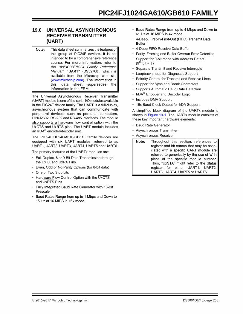
PIC24FJ1024GA610/GB610 FAMILY
19.0 UNIVERSAL ASYNCHRONOUS RECEIVER TRANSMITTER (UART)
The Universal Asynchronous Receiver Transmitter(UART) module is one of the serial I/O modules availablein the PIC24F device family. The UART is a full-duplex,asynchronous system that can communicate withperipheral devices, such as personal computers,LIN/J2602, RS-232 and RS-485 interfaces. The modulealso supports a hardware flow control option with theUxCTS and UxRTS pins. The UART module includesan IrDA® encoder/decoder unit.
The PIC24FJ1024GA610/GB610 family devices areequipped with six UART modules, referred to asUART1, UART2, UART3, UART4, UART5 and UART6.
The primary features of the UARTx modules are:
• Full-Duplex, 8 or 9-Bit Data Transmission through the UxTX and UxRX Pins
• Even, Odd or No Parity Options (for 8-bit data)
• One or Two Stop bits
• Hardware Flow Control Option with the UxCTS and UxRTS Pins
• Fully Integrated Baud Rate Generator with 16-Bit Prescaler
• Baud Rates Range from up to 1 Mbps and Down to 15 Hz at 16 MIPS in 16x mode
• Baud Rates Range from up to 4 Mbps and Down to 61 Hz at 16 MIPS in 4x mode
• 4-Deep, First-In-First-Out (FIFO) Transmit Data Buffer
• 4-Deep FIFO Receive Data Buffer
• Parity, Framing and Buffer Overrun Error Detection
• Support for 9-bit mode with Address Detect (9th bit = 1)
• Separate Transmit and Receive Interrupts
• Loopback mode for Diagnostic Support
• Polarity Control for Transmit and Receive Lines
• Support for Sync and Break Characters
• Supports Automatic Baud Rate Detection
• IrDA® Encoder and Decoder Logic
• Includes DMA Support
• 16x Baud Clock Output for IrDA Support
A simplified block diagram of the UARTx module isshown in Figure 19-1. The UARTx module consists ofthese key important hardware elements:
• Baud Rate Generator
• Asynchronous Transmitter
• Asynchronous Receiver
Note: This data sheet summarizes the features ofthis group of PIC24F devices. It is notintended to be a comprehensive referencesource. For more information, refer tothe “dsPIC33/PIC24 Family ReferenceManual”, “UART” (DS39708), which isavailable from the Microchip web site(www.microchip.com). The information inthis data sheet supersedes theinformation in the FRM.
Note: Throughout this section, references toregister and bit names that may be asso-ciated with a specific UART module arereferred to generically by the use of ‘x’ inplace of the specific module number.Thus, “UxSTA” might refer to the Statusregister for either UART1, UART2,UART3, UART4, UART5 or UART6.
2015-2017 Microchip Technology Inc. DS30010074E-page 255

PIC24FJ1024GA610/GB610 FAMILY
FIGURE 19-1: UARTx SIMPLIFIED BLOCK DIAGRAM
IrDA®
UARTx Receiver
UxTX (1)
UxCTS(1)
UxRTS/BCLKx(1)
Note 1: The UART1, UART2, UART3 and UART4 inputs and outputs must all be assigned to available RPn/RPIn pins before use. See Section 11.4 “Peripheral Pin Select (PPS)” for more information.
Baud Rate Generator
UARTx Transmitter
UxRX (1)
Hardware Flow Control
DS30010074E-page 256 2015-2017 Microchip Technology Inc.

PIC24FJ1024GA610/GB610 FAMILY
19.1 UARTx Baud Rate Generator (BRG)
The UARTx module includes a dedicated, 16-bit BaudRate Generator. The UxBRG register controls theperiod of a free-running, 16-bit timer. Equation 19-1shows the formula for computation of the baud ratewhen BRGH = 0.
EQUATION 19-1: UARTx BAUD RATE WITH BRGH = 0(1,2)
Example 19-1 shows the calculation of the baud rateerror for the following conditions:
• FCY = 4 MHz
• Desired Baud Rate = 9600
The maximum baud rate (BRGH = 0) possible isFCY/16 (for UxBRG = 0) and the minimum baud ratepossible is FCY/(16 * 65536).
Equation 19-2 shows the formula for computation ofthe baud rate when BRGH = 1.
EQUATION 19-2: UARTx BAUD RATE WITH BRGH = 1(1,2)
The maximum baud rate (BRGH = 1) possible is FCY/4(for UxBRG = 0) and the minimum baud rate possibleis FCY/(4 * 65536).
Writing a new value to the UxBRG register causes theBRG timer to be reset (cleared). This ensures the BRGdoes not wait for a timer overflow before generating thenew baud rate.
EXAMPLE 19-1: BAUD RATE ERROR CALCULATION (BRGH = 0)(1)
Note 1: FCY denotes the instruction cycle clock frequency (FOSC/2).
2: Based on FCY = FOSC/2; Doze mode and PLL are disabled.
Baud Rate =FCY
16 • (UxBRG + 1)
UxBRG =FCY
16 • Baud Rate– 1
Note 1: FCY denotes the instruction cycle clock frequency.
2: Based on FCY = FOSC/2; Doze mode and PLL are disabled.
Baud Rate =FCY
4 • (UxBRG + 1)
UxBRG =FCY
4 • Baud Rate– 1
Note 1: Based on FCY = FOSC/2; Doze mode and PLL are disabled.
Desired Baud Rate = FCY/(16 (UxBRG + 1))
Solving for UxBRG Value:
UxBRG = ((FCY/Desired Baud Rate)/16) – 1UxBRG = ((4000000/9600)/16) – 1 UxBRG = 25
Calculated Baud Rate = 4000000/(16 (25 + 1)) = 9615
Error = (Calculated Baud Rate – Desired Baud Rate)Desired Baud Rate
= (9615 – 9600)/9600 = 0.16%
2015-2017 Microchip Technology Inc. DS30010074E-page 257
PIC24FJ1024GA610/GB610 FAMILY
19.2 Transmitting in 8-Bit Data Mode
1. Set up the UARTx:
a) Write appropriate values for data, parity andStop bits.
b) Write appropriate baud rate value to theUxBRG register.
c) Set up transmit and receive interrupt enableand priority bits.
2. Enable the UARTx.
3. Set the UTXEN bit (causes a transmit interrupt,two cycles after being set).
4. Write a data byte to the lower byte of theUxTXREG word. The value will be immediatelytransferred to the Transmit Shift Register (TSR)and the serial bit stream will start shifting outwith the next rising edge of the baud clock.
5. Alternatively, the data byte may be transferredwhile UTXEN = 0 and then the user may setUTXEN. This will cause the serial bit stream tobegin immediately because the baud clock willstart from a cleared state.
6. A transmit interrupt will be generated as perinterrupt control bits, UTXISEL<1:0>.
19.3 Transmitting in 9-Bit Data Mode
1. Set up the UARTx (as described in Section 19.2“Transmitting in 8-Bit Data Mode”).
2. Enable the UARTx.
3. Set the UTXEN bit (causes a transmit interrupt).
4. Write UxTXREG as a 16-bit value only.
5. A word write to UxTXREG triggers the transferof the 9-bit data to the TSR. The serial bit streamwill start shifting out with the first rising edge ofthe baud clock.
6. A transmit interrupt will be generated as per thesetting of control bits, UTXISELx.
19.4 Break and Sync Transmit Sequence
The following sequence will send a message frameheader, made up of a Break, followed by an auto-baudSync byte.
1. Configure the UARTx for the desired mode.
2. Set UTXEN and UTXBRK to set up the Breakcharacter.
3. Load the UxTXREG with a dummy character toinitiate transmission (value is ignored).
4. Write ‘55h’ to UxTXREG; this loads the Synccharacter into the transmit FIFO.
5. After the Break has been sent, the UTXBRK bitis reset by hardware. The Sync character nowtransmits.
19.5 Receiving in 8-Bit or 9-Bit Data Mode
1. Set up the UARTx (as described in Section 19.2“Transmitting in 8-Bit Data Mode”).
2. Enable the UARTx by setting the URXEN bit(UxSTA<12>).
3. A receive interrupt will be generated when oneor more data characters have been received asper interrupt control bits, URXISEL<1:0>.
4. Read the OERR bit to determine if an overrunerror has occurred. The OERR bit must be resetin software.
5. Read UxRXREG.
The act of reading the UxRXREG character will movethe next character to the top of the receive FIFO,including a new set of PERR and FERR values.
19.6 Operation of UxCTS and UxRTS Control Pins
UARTx Clear-to-Send (UxCTS) and Request-to-Send(UxRTS) are the two hardware-controlled pins that areassociated with the UARTx modules. These two pinsallow the UARTx to operate in Simplex and FlowControl mode. They are implemented to control thetransmission and reception between the Data TerminalEquipment (DTE). The UEN<1:0> bits in the UxMODEregister configure these pins.
19.7 Infrared Support
The UARTx module provides two types of infraredUART support: one is the IrDA clock output to supportan external IrDA encoder and decoder device (legacymodule support), and the other is the full implementa-tion of the IrDA encoder and decoder. Note thatbecause the IrDA modes require a 16x baud clock, theywill only work when the BRGH bit (UxMODE<3>) is ‘0’.
19.7.1 IrDA CLOCK OUTPUT FOR EXTERNAL IrDA SUPPORT
To support external IrDA encoder and decoder devices,the BCLKx pin (same as the UxRTS pin) can beconfigured to generate the 16x baud clock. WhenUEN<1:0> = 11, the BCLKx pin will output the16x baud clock if the UARTx module is enabled; it canbe used to support the IrDA codec chip.
19.7.2 BUILT-IN IrDA ENCODER AND DECODER
The UARTx has full implementation of the IrDAencoder and decoder as part of the UARTx module.The built-in IrDA encoder and decoder functionality isenabled using the IREN bit (UxMODE<12>). Whenenabled (IREN = 1), the receive pin (UxRX) acts as theinput from the infrared receiver. The transmit pin(UxTX) acts as the output to the infrared transmitter.
DS30010074E-page 258 2015-2017 Microchip Technology Inc.
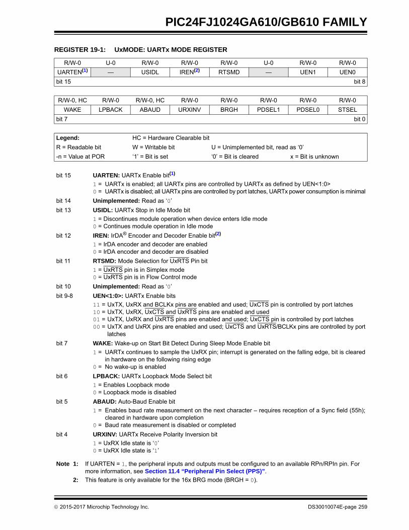
PIC24FJ1024GA610/GB610 FAMILY
REGISTER 19-1: UxMODE: UARTx MODE REGISTER
R/W-0 U-0 R/W-0 R/W-0 R/W-0 U-0 R/W-0 R/W-0
UARTEN(1) — USIDL IREN(2) RTSMD — UEN1 UEN0
bit 15 bit 8
R/W-0, HC R/W-0 R/W-0, HC R/W-0 R/W-0 R/W-0 R/W-0 R/W-0
WAKE LPBACK ABAUD URXINV BRGH PDSEL1 PDSEL0 STSEL
bit 7 bit 0
Legend: HC = Hardware Clearable bit
R = Readable bit W = Writable bit U = Unimplemented bit, read as ‘0’
-n = Value at POR ‘1’ = Bit is set ‘0’ = Bit is cleared x = Bit is unknown
bit 15 UARTEN: UARTx Enable bit(1)
1 = UARTx is enabled; all UARTx pins are controlled by UARTx as defined by UEN<1:0>0 = UARTx is disabled; all UARTx pins are controlled by port latches, UARTx power consumption is minimal
bit 14 Unimplemented: Read as ‘0’
bit 13 USIDL: UARTx Stop in Idle Mode bit
1 = Discontinues module operation when device enters Idle mode0 = Continues module operation in Idle mode
bit 12 IREN: IrDA® Encoder and Decoder Enable bit(2)
1 = IrDA encoder and decoder are enabled0 = IrDA encoder and decoder are disabled
bit 11 RTSMD: Mode Selection for UxRTS Pin bit
1 = UxRTS pin is in Simplex mode0 = UxRTS pin is in Flow Control mode
bit 10 Unimplemented: Read as ‘0’
bit 9-8 UEN<1:0>: UARTx Enable bits
11 = UxTX, UxRX and BCLKx pins are enabled and used; UxCTS pin is controlled by port latches10 = UxTX, UxRX, UxCTS and UxRTS pins are enabled and used01 = UxTX, UxRX and UxRTS pins are enabled and used; UxCTS pin is controlled by port latches00 = UxTX and UxRX pins are enabled and used; UxCTS and UxRTS/BCLKx pins are controlled by port
latches
bit 7 WAKE: Wake-up on Start Bit Detect During Sleep Mode Enable bit
1 = UARTx continues to sample the UxRX pin; interrupt is generated on the falling edge, bit is clearedin hardware on the following rising edge
0 = No wake-up is enabled
bit 6 LPBACK: UARTx Loopback Mode Select bit
1 = Enables Loopback mode0 = Loopback mode is disabled
bit 5 ABAUD: Auto-Baud Enable bit
1 = Enables baud rate measurement on the next character – requires reception of a Sync field (55h);cleared in hardware upon completion
0 = Baud rate measurement is disabled or completed
bit 4 URXINV: UARTx Receive Polarity Inversion bit
1 = UxRX Idle state is ‘0’0 = UxRX Idle state is ‘1’
Note 1: If UARTEN = 1, the peripheral inputs and outputs must be configured to an available RPn/RPIn pin. For more information, see Section 11.4 “Peripheral Pin Select (PPS)”.
2: This feature is only available for the 16x BRG mode (BRGH = 0).
2015-2017 Microchip Technology Inc. DS30010074E-page 259

PIC24FJ1024GA610/GB610 FAMILY
bit 3 BRGH: High Baud Rate Enable bit
1 = High-Speed mode (4 BRG clock cycles per bit)0 = Standard Speed mode (16 BRG clock cycles per bit)
bit 2-1 PDSEL<1:0>: Parity and Data Selection bits
11 = 9-bit data, no parity10 = 8-bit data, odd parity01 = 8-bit data, even parity00 = 8-bit data, no parity
bit 0 STSEL: Stop Bit Selection bit
1 = Two Stop bits0 = One Stop bit
REGISTER 19-1: UxMODE: UARTx MODE REGISTER (CONTINUED)
Note 1: If UARTEN = 1, the peripheral inputs and outputs must be configured to an available RPn/RPIn pin. For more information, see Section 11.4 “Peripheral Pin Select (PPS)”.
2: This feature is only available for the 16x BRG mode (BRGH = 0).
DS30010074E-page 260 2015-2017 Microchip Technology Inc.

PIC24FJ1024GA610/GB610 FAMILY
REGISTER 19-2: UxSTA: UARTx STATUS AND CONTROL REGISTER
R/W-0 R/W-0 R/W-0 R/W-0 R/W-0, HC R/W-0 R-0, HSC R-1, HSC
UTXISEL1 UTXINV(1) UTXISEL0 URXEN UTXBRK UTXEN(2) UTXBF TRMT
bit 15 bit 8
R/W-0 R/W-0 R/W-0 R-1, HSC R-0, HSC R-0, HSC R/C-0, HS R-0, HSC
URXISEL1 URXISEL0 ADDEN RIDLE PERR FERR OERR URXDA
bit 7 bit 0
Legend: C = Clearable bit HSC = Hardware Settable/Clearable bit
R = Readable bit W = Writable bit U = Unimplemented bit, read as ‘0’
-n = Value at POR ‘1’ = Bit is set ‘0’ = Bit is cleared x = Bit is unknown
HS = Hardware Settable bit HC = Hardware Clearable bit
bit 15,13 UTXISEL<1:0>: UARTx Transmission Interrupt Mode Selection bits
11 = Reserved; do not use10 = Interrupt when a character is transferred to the Transmit Shift Register (TSR), and as a result, the
transmit buffer becomes empty01 = Interrupt when the last character is shifted out of the Transmit Shift Register; all transmit
operations are completed00 = Interrupt when a character is transferred to the Transmit Shift Register (this implies there is at least
one character open in the transmit buffer)
bit 14 UTXINV: UARTx IrDA® Encoder Transmit Polarity Inversion bit(1)
IREN = 0:1 = UxTX Idle state is ‘0’0 = UxTX Idle state is ‘1’
IREN = 1:1 = UxTX Idle state is ‘1’0 = UxTX Idle state is ‘0’
bit 12 URXEN: UARTx Receive Enable bit
1 = Receive is enabled, UxRX pin is controlled by UARTx0 = Receive is disabled, UxRX pin is controlled by the port
bit 11 UTXBRK: UARTx Transmit Break bit
1 = Sends Sync Break on next transmission – Start bit, followed by twelve ‘0’ bits, followed by Stop bit;cleared by hardware upon completion
0 = Sync Break transmission is disabled or completed
bit 10 UTXEN: UARTx Transmit Enable bit(2)
1 = Transmit is enabled, UxTX pin is controlled by UARTx0 = Transmit is disabled, any pending transmission is aborted and the buffer is reset; UxTX pin is
controlled by the port
bit 9 UTXBF: UARTx Transmit Buffer Full Status bit (read-only)
1 = Transmit buffer is full0 = Transmit buffer is not full, at least one more character can be written
bit 8 TRMT: Transmit Shift Register Empty bit (read-only)
1 = Transmit Shift Register is empty and transmit buffer is empty (the last transmission has completed)0 = Transmit Shift Register is not empty, a transmission is in progress or queued
Note 1: The value of this bit only affects the transmit properties of the module when the IrDA® encoder is enabled (IREN = 1).
2: If UARTEN = 1, the peripheral inputs and outputs must be configured to an available RPn/RPIn pin. For more information, see Section 11.4 “Peripheral Pin Select (PPS)”.
2015-2017 Microchip Technology Inc. DS30010074E-page 261

PIC24FJ1024GA610/GB610 FAMILY
bit 7-6 URXISEL<1:0>: UARTx Receive Interrupt Mode Selection bits
11 = Interrupt is set on an RSR transfer, making the receive buffer full (i.e., has 4 data characters)10 = Interrupt is set on an RSR transfer, making the receive buffer 3/4 full (i.e., has 3 data characters)0x = Interrupt is set when any character is received and transferred from the RSR to the receive buffer;
receive buffer has one or more characters
bit 5 ADDEN: Address Character Detect bit (bit 8 of received data = 1)
1 = Address Detect mode is enabled (if 9-bit mode is not selected, this does not take effect)0 = Address Detect mode is disabled
bit 4 RIDLE: Receiver Idle bit (read-only)
1 = Receiver is Idle0 = Receiver is active
bit 3 PERR: Parity Error Status bit (read-only)
1 = Parity error has been detected for the current character (the character at the top of the receive FIFO)0 = Parity error has not been detected
bit 2 FERR: Framing Error Status bit (read-only)
1 = Framing error has been detected for the current character (the character at the top of the receive FIFO)0 = Framing error has not been detected
bit 1 OERR: Receive Buffer Overrun Error Status bit (clear/read-only)
1 = Receive buffer has overflowed0 = Receive buffer has not overflowed (clearing a previously set OERR bit, 1 0 transition); will reset
the receive buffer and the RSR to the empty state
bit 0 URXDA: UARTx Receive Buffer Data Available bit (read-only)
1 = Receive buffer has data, at least one more character can be read0 = Receive buffer is empty
REGISTER 19-2: UxSTA: UARTx STATUS AND CONTROL REGISTER (CONTINUED)
Note 1: The value of this bit only affects the transmit properties of the module when the IrDA® encoder is enabled (IREN = 1).
2: If UARTEN = 1, the peripheral inputs and outputs must be configured to an available RPn/RPIn pin. For more information, see Section 11.4 “Peripheral Pin Select (PPS)”.
DS30010074E-page 262 2015-2017 Microchip Technology Inc.

PIC24FJ1024GA610/GB610 FAMILY
REGISTER 19-3: UxRXREG: UARTx RECEIVE REGISTER (NORMALLY READ-ONLY)
U-0 U-0 U-0 U-0 U-0 U-0 U-0 R-0
— — — — — — — UxRXREG8
bit 15 bit 8
R-0 R-0 R-0 R-0 R-0 R-0 R-0 R-0
UxRXREG<7:0>
bit 7 bit 0
Legend:
R = Readable bit W = Writable bit U = Unimplemented bit, read as ‘0’
-n = Value at POR ‘1’ = Bit is set ‘0’ = Bit is cleared x = Bit is unknown
bit 15-9 Unimplemented: Read as ‘0’
bit 8-0 UxRXREG<8:0>: Data of the Received Character bits
REGISTER 19-4: UxTXREG: UARTx TRANSMIT REGISTER (NORMALLY WRITE-ONLY)
U-0 U-0 U-0 U-0 U-0 U-0 U-0 W-x
— — — — — — — UxTXREG8
bit 15 bit 8
W-x W-x W-x W-x W-x W-x W-x W-x
UxTXREG<7:0>
bit 7 bit 0
Legend:
R = Readable bit W = Writable bit U = Unimplemented bit, read as ‘0’
-n = Value at POR ‘1’ = Bit is set ‘0’ = Bit is cleared x = Bit is unknown
bit 15-9 Unimplemented: Read as ‘0’
bit 8-0 UxTXREG<8:0>: Data of the Transmitted Character bits
2015-2017 Microchip Technology Inc. DS30010074E-page 263

PIC24FJ1024GA610/GB610 FAMILY
REGISTER 19-5: UxBRG: UARTx BAUD RATE GENERATOR REGISTER
R/W-0 R/W-0 R/W-0 R/W-0 R/W-0 R/W-0 R/W-0 R/W-0
BRG<15:8>
bit 15 bit 8
R/W-0 R/W-0 R/W-0 R/W-0 R/W-0 R/W-0 R/W-0 R/W-0
BRG<7:0>
bit 7 bit 0
Legend:
R = Readable bit W = Writable bit U = Unimplemented bit, read as ‘0’
-n = Value at POR ‘1’ = Bit is set ‘0’ = Bit is cleared x = Bit is unknown
bit 15-0 BRG<15:0>: Baud Rate Divisor bits
REGISTER 19-6: UxADMD: UARTx ADDRESS DETECT AND MATCH REGISTER
R/W-0 R/W-0 R/W-0 R/W-0 R/W-0 R/W-0 R/W-0 R/W-0
ADMMASK7 ADMMASK6 ADMMASK5 ADMMASK4 ADMMASK3 ADMMASK2 ADMMASK1 ADMMASK0
bit 15 bit 8
R/W-0 R/W-0 R/W-0 R/W-0 R/W-0 R/W-0 R/W-0 R/W-0
ADMADDR7 ADMADDR6 ADMADDR5 ADMADDR4 ADMADDR3 ADMADDR2 ADMADDR1 ADMADDR0
bit 7 bit 0
Legend:
R = Readable bit W = Writable bit U = Unimplemented bit, read as ‘0’
-n = Value at POR ‘1’ = Bit is set ‘0’ = Bit is cleared x = Bit is unknown
bit 15-8 ADMMASK<7:0>: ADMADDR<7:0> (UxADMD<7:0>) Masking bits
For ADMMASKx:1 = ADMADDRx is used to detect the address match0 = ADMADDRx is not used to detect the address match
bit 7-0 ADMADDR<7:0>: Address Detect Task Off-Load bits
Used with the ADMMASK<7:0> bits (UxADMD<15:8>) to off-load the task of detecting the addresscharacter from the processor during Address Detect mode.
DS30010074E-page 264 2015-2017 Microchip Technology Inc.

PIC24FJ1024GA610/GB610 FAMILY
20.0 UNIVERSAL SERIAL BUS WITH ON-THE-GO SUPPORT (USB OTG)
PIC24FJ1024GB610 family devices contain a full-speed and low-speed compatible, On-The-Go (OTG)USB Serial Interface Engine (SIE). The OTG capabilityallows the device to act as either a USB peripheraldevice or as a USB embedded host with limited hostcapabilities. The OTG capability allows the device todynamically switch from device to host operation usingOTG’s Host Negotiation Protocol (HNP).
For more details on OTG operation, refer to the “On-The-Go Supplement” to the “USB 2.0 Specification”,published by the USB-IF. For more details on USBoperation, refer to the “Universal Serial BusSpecification”, v2.0.
The USB OTG module offers these features:
• USB Functionality in Device and Host modes, and OTG Capabilities for Application-Controlled mode Switching
• Software-Selectable module Speeds of Full Speed (12 Mbps) or Low Speed (1.5 Mbps available in Host mode only)
• Support for All Four USB Transfer Types: Control, Interrupt, Bulk and Isochronous
• 16 Bidirectional Endpoints for a Total of 32 Unique Endpoints
• DMA Interface for Data RAM Access
• Queues up to 16 Unique Endpoint Transfers without Servicing
• Integrated, On-Chip USB Transceiver with Support for Off-Chip Transceivers via a Digital Interface
• Integrated VBUS Generation with On-Chip Comparators and Boost Generation, and Support of External VBUS Comparators and Regulators through a Digital Interface
• Configurations for On-Chip Bus Pull-up and Pull-Down Resistors
A simplified block diagram of the USB OTG module isshown in Figure 20-1.
The USB OTG module can function as a USB peripheraldevice or as a USB host, and may dynamically switchbetween Device and Host modes under softwarecontrol. In either mode, the same data paths and BufferDescriptors (BDs) are used for the transmission andreception of data.
In discussing USB operation, this section will use acontroller-centric nomenclature for describing the direc-tion of the data transfer between the microcontroller andthe USB. RX (Receive) will be used to describe transfersthat move data from the USB to the microcontroller andTX (Transmit) will be used to describe transfers thatmove data from the microcontroller to the USB.Table 20-1 shows the relationship between datadirection in this nomenclature and the USB tokensexchanged.
TABLE 20-1: CONTROLLER-CENTRIC DATA DIRECTION FOR USB HOST OR TARGET
This chapter presents the most basic operationsneeded to implement USB OTG functionality in anapplication. A complete and detailed discussion of theUSB protocol and its OTG supplement are beyond thescope of this data sheet. It is assumed that the useralready has a basic understanding of USB architectureand the latest version of the protocol.
Not all steps for proper USB operation (such as deviceenumeration) are presented here. It is recommendedthat application developers use an appropriate devicedriver to implement all of the necessary features.Microchip provides a number of application-specificresources, such as USB firmware and driver support.Refer to www.microchip.com/usb for the latestfirmware and driver support.
Note: This data sheet summarizes the features ofthis group of PIC24F devices. It is notintended to be a comprehensive referencesource. For more information, refer tothe “dsPIC33/PIC24 Family ReferenceManual”, “USB On-The-Go (OTG)”(DS39721), which is available from theMicrochip web site (www.microchip.com).The information in this data sheetsupersedes the information in the FRM.
USB ModeDirection
RX TX
Device OUT or SETUP IN
Host IN OUT or SETUP
2015-2017 Microchip Technology Inc. DS30010074E-page 265

PIC24FJ1024GA610/GB610 FAMILY
FIGURE 20-1: USB OTG MODULE BLOCK DIAGRAM
48 MHz USB Clock
D+(1)
D-(1)
USBID(1)
VBUS(1)
Transceiver
Comparators
USB
SRP Charge
SRP Discharge
Registersand
ControlInterface
Voltage
System
RAM
Full-Speed Pull-up
Host Pull-Down
Host Pull-Down
Note 1: Pins are multiplexed with digital I/O and other device features.2: Connecting VBUS3V3 to VDD is highly recommended, as floating this input can cause increased IPD currents. The
pin should be tied to VDD when the USB functions are not used.
RCV(1)
VBUS
BoostAssist
External Transceiver Interface
USBOEN(1)
Transceiver Power 3.3V VUSB3V3(2)
SIE
USB
DS30010074E-page 266 2015-2017 Microchip Technology Inc.

PIC24FJ1024GA610/GB610 FAMILY
20.1 Hardware Configuration
20.1.1 DEVICE MODE
20.1.1.1 D+ Pull-up Resistor
PIC24FJ1024GB610 family devices have a built-in1.5 k resistor on the D+ line that is available when themicrocontroller is operating in Device mode. This isused to signal an external host that the device isoperating in Full-Speed Device mode. It is engaged bysetting the USBEN bit (U1CON<0>) and powering upthe USB module (USBPWR = 1). If the OTGEN bit(U1OTGCON<2>) is set, then the D+ pull-up is enabledthrough the DPPULUP bit (U1OTGCON<7>).
20.1.1.2 The VBUS Pin
In order to meet the “USB 2.0 Specification” require-ment, relating to the back drive voltage on the D+/D-pins, the USB module incorporates VBUS-level sensingcomparators. When the comparators detect the VBUS
level below the VA_SESS_VLD level, the hardware willautomatically disable the D+ pull-up resistor describedin Section 20.1.1.1 “D+ Pull-up Resistor”. Thisallows the device to automatically meet the back driverequirement for D+ and D-, even if the application firm-ware does not explicitly monitor the VBUS level. There-fore, the VBUS microcontroller pin should not be leftfloating in USB Device mode application designs, andshould normally be connected to the VBUS pin on theUSB connector/cable (either directly or through a smallresistance 100 ohms).
20.1.1.3 Power Modes
Many USB applications will likely have several differentsets of power requirements and configuration. Themost common power modes encountered are:
• Bus Power Only mode
• Self-Power Only mode
• Dual Power with Self-Power Dominance
Bus Power Only mode (Figure 20-2) is effectively thesimplest method. All power for the application is drawnfrom the USB.
To meet the inrush current requirements of the“USB 2.0 Specification”, the total effective capacitance,appearing across VBUS and ground, must be no morethan 10 F.
In the USB Suspend mode, devices must consume nomore than 2.5 mA from the 5V VBUS line of the USBcable. During the USB Suspend mode, the D+ or D-pull-up resistor must remain active, which will consumesome of the allowed suspend current.
In Self-Power Only mode (Figure 20-3), the USBapplication provides its own power, with very littlepower being pulled from the USB. Note that an attachindication is added to indicate when the USB has beenconnected and the host is actively powering VBUS.
To meet compliance specifications, the USB module(and the D+ or D- pull-up resistor) should not be enableduntil the host actively drives VBUS high. One of the 5.5Vtolerant I/O pins may be used for this purpose.
The application should never source any current ontothe 5V VBUS pin of the USB cable when the USBmodule is operated in USB Device mode.
The Dual Power mode with Self-Power Dominance(Figure 20-4) allows the application to use internalpower primarily, but switch to power from the USBwhen no internal power is available. Dual powerdevices must also meet all of the special requirementsfor inrush current and Suspend mode current previ-ously described, and must not enable the USB moduleuntil VBUS is driven high.
FIGURE 20-2: BUS-POWERED INTERFACE EXAMPLE
FIGURE 20-3: SELF-POWER ONLY
FIGURE 20-4: DUAL POWER EXAMPLE
VDD
VUSB3V3
VSS
VBUS~5V
3.3V
MCP1801
Attach SenseVBUS
100
3.3V LDO
1 F
VDD
VUSB3V3
VSS
VSELF~3.3V
Attach Sense
100 k
100VBUS~5V VBUS
VDD
VUSB3V3
VBUS
VSS
Attach Sense
VBUS
VSELF
100
~3.3V
~5V
100 k
3.3V
Low IQRegulator
2015-2017 Microchip Technology Inc. DS30010074E-page 267

PIC24FJ1024GA610/GB610 FAMILY
20.1.2 HOST AND OTG MODES
20.1.2.1 D+ and D- Pull-Down Resistors
PIC24FJ1024GB610 family devices have a built-in 15 kpull-down resistor on the D+ and D- lines. These areused in tandem to signal to the bus that the micro-controller is operating in Host mode. They are engagedby setting the HOSTEN bit (U1CON<3>). If the OTGENbit (U1OTGCON<2>) is set, then these pull-downs areenabled by setting the DPPULDWN and DMPULDWNbits (U1OTGCON<5:4>).
20.1.2.2 Power Configurations
In Host mode, as well as Host mode in On-The-Gooperation, the “USB 2.0 Specification” requires that thehost application should supply power on VBUS. Sincethe microcontroller is running below VBUS, and is notable to source sufficient current, a separate powersupply must be provided.
When the application is always operating in Host mode,a simple circuit can be used to supply VBUS andregulate current on the bus (Figure 20-5). For OTGoperation, it is necessary to be able to turn VBUS on oroff as needed, as the microcontroller switches betweenDevice and Host modes. A typical example using anexternal charge pump is shown in Figure 20-6.
FIGURE 20-5: HOST INTERFACE EXAMPLE
FIGURE 20-6: OTG INTERFACE EXAMPLE
A/D Pin
VUSB3V3
VDD
VSS
D+D-
VBUS
ID
D+D-
VBUS
IDGND
+3.3V +3.3V
Polymer PTCThermal Fuse
Micro A/BConnector
150 µF
2 k
2 k
0.1 µF3.3V
+5VPIC® MCU
I/OI/O
VSS
D+D-
VBUS
ID
Micro A/BConnector
40 k4.7 µF
VDD PIC® MCU
10 µFVIN
SELECT
SHNDPGOOD
MCP1253
VOUT
C+
C-
GND
1 µF
D+D-
VBUS
IDGND
VUSB3V3
VDD
+3.3V +3.3V
0.1 µF3.3V
DS30010074E-page 268 2015-2017 Microchip Technology Inc.

PIC24FJ1024GA610/GB610 FAMILY
20.1.3 CALCULATING TRANSCEIVER POWER REQUIREMENTS
The USB transceiver consumes a variable amount ofcurrent depending on the characteristic impedance ofthe USB cable, the length of the cable, the VUSB supplyvoltage and the actual data patterns moving across theUSB cable. Longer cables have larger capacitancesand consume more total energy when switching output
states. The total transceiver current consumptionwill be application-specific. Equation 20-1 can helpestimate how much current actually may be required infull-speed applications.
Refer to the “dsPIC33/PIC24 Family ReferenceManual”, “USB On-The-Go (OTG)” (DS39721) for acomplete discussion on transceiver power consumption.
EQUATION 20-1: ESTIMATING USB TRANSCEIVER CURRENT CONSUMPTION
Legend: VUSB – Voltage applied to the VUSB3V3 pin in volts (3.0V to 3.6V).
PZERO – Percentage (in decimal) of the IN traffic bits sent by the PIC® microcontroller that are a valueof ‘0’.
PIN – Percentage (in decimal) of total bus bandwidth that is used for IN traffic.
LCABLE – Length (in meters) of the USB cable. The “USB 2.0 Specification” requires that full-speedapplications use cables no longer than 5m.
IPULLUP – Current which the nominal, 1.5 k pull-up resistor (when enabled) must supply to theUSB cable.
40 mA • VUSB • PZERO • PIN • LCABLEIXCVR =
3.3V • 5m+ IPULLUP
2015-2017 Microchip Technology Inc. DS30010074E-page 269

PIC24FJ1024GA610/GB610 FAMILY
20.2 USB Buffer Descriptors and the BDT
Endpoint buffer control is handled through a structurecalled the Buffer Descriptor Table (BDT). This providesa flexible method for users to construct and controlendpoint buffers of various lengths and configurations.
The BDT can be located in any available 512-byte,aligned block of data RAM. The BDT Pointer(U1BDTP1) contains the upper address byte of theBDT and sets the location of the BDT in RAM. The usermust set this pointer to indicate the table’s location.
The BDT is composed of Buffer Descriptors (BDs)which are used to define and control the actual buffersin the USB RAM space. Each BD consists of two 16-bit,“soft” (non-fixed-address) registers, BDnSTAT andBDnADR, where n represents one of the 64 possibleBDs (range of 0 to 63). BDnSTAT is the status registerfor BDn, while BDnADR specifies the starting addressfor the buffer associated with BDn.
Depending on the endpoint buffering configurationused, there are up to 64 sets of Buffer Descriptors, fora total of 256 bytes. At a minimum, the BDT must be atleast 8 bytes long. This is because the “USB 2.0Specification” mandates that every device must haveEndpoint 0 with both input and output for initial setup.
Endpoint mapping in the BDT is dependent on threevariables:
• Endpoint number (0 to 15)
• Endpoint direction (RX or TX)
• Ping-pong settings (U1CNFG1<1:0>)
Figure 20-7 illustrates how these variables are used tomap endpoints in the BDT.
In Host mode, only Endpoint 0 Buffer Descriptors areused. All transfers utilize the Endpoint 0 Buffer Descrip-tor and Endpoint Control register (U1EP0). For receivedpackets, the attached device’s source endpoint isindicated by the value of ENDPT<3:0> in the USB Statusregister (U1STAT<7:4>). For transmitted packets, theattached device’s destination endpoint is indicated bythe value written to the USB Token register (U1TOK).
FIGURE 20-7: BDT MAPPING FOR ENDPOINT BUFFERING MODES
Note: Since BDnADR is a 16-bit register, onlythe first 64 Kbytes of RAM can beaccessed by the USB module.
EP1 TX Even
EP1 RX Even
EP1 RX Odd
EP1 TX Odd
Descriptor
Descriptor
Descriptor
Descriptor
EP1 TX
EP15 TX
EP1 RX
EP0 RX
PPB<1:0> = 00
EP0 TX
EP1 TX
No Ping-Pong
EP15 TX
EP0 TX
EP0 RX Even
PPB<1:0> = 01
EP0 RX Odd
EP1 RX
Ping-Pong Buffer
EP15 TX Odd
EP0 TX Even
EP0 RX Even
PPB<1:0> = 10
EP0 RX Odd
EP0 TX Odd
Ping-Pong Buffers
Descriptor
Descriptor
Descriptor
Descriptor
Descriptor
Descriptor
Descriptor
Descriptor
Descriptor
Descriptor
Descriptor
Descriptor
Note: Memory area is not shown to scale.
Descriptor
Descriptor
Descriptor
Descriptor
Buffers on EP0 RX on All EPs
EP1 TX Even
EP1 RX Even
EP1 RX Odd
EP1 TX Odd
Descriptor
Descriptor
Descriptor
Descriptor
EP15 TX Odd
EP0 RX
PPB<1:0> = 11
EP0 TX
Ping-Pong Buffers
Descriptor
Descriptor
Descriptor
on All Other EPsExcept EP0
Total BDT Space: Total BDT Space: Total BDT Space: Total BDT Space:128 Bytes 132 Bytes 256 Bytes 248 Bytes
DS30010074E-page 270 2015-2017 Microchip Technology Inc.

PIC24FJ1024GA610/GB610 FAMILY
BDs have a fixed relationship to a particular endpoint,depending on the buffering configuration. Table 20-2provides the mapping of BDs to endpoints. This rela-tionship also means that gaps may occur in the BDT ifendpoints are not enabled contiguously. This, theoreti-cally, means that the BDs for disabled endpoints couldbe used as buffer space. In practice, users shouldavoid using such spaces in the BDT unless a methodof validating BD addresses is implemented.
20.2.1 BUFFER OWNERSHIP
Because the buffers and their BDs are shared betweenthe CPU and the USB module, a simple semaphoremechanism is used to distinguish which is allowed toupdate the BD and associated buffers in memory. Thisis done by using the UOWN bit as a semaphore todistinguish which is allowed to update the BD andassociated buffers in memory. UOWN is the only bitthat is shared between the two configurations ofBDnSTAT.
When UOWN is clear, the BD entry is “owned” by themicrocontroller core. When the UOWN bit is set, the BDentry and the buffer memory are “owned” by the USBperipheral. The core should not modify the BD or its
corresponding data buffer during this time. Note thatthe microcontroller core can still read BDnSTAT whilethe SIE owns the buffer and vice versa.
The Buffer Descriptors have a different meaning basedon the source of the register update. Register 20-1 andRegister 20-2 show the differences in BDnSTATdepending on its current “ownership”.
When UOWN is set, the user can no longer depend onthe values that were written to the BDs. From this point,the USB module updates the BDs as necessary, over-writing the original BD values. The BDnSTAT register isupdated by the SIE with the token PID and the transfercount is updated.
20.2.2 DMA INTERFACE
The USB OTG module uses a dedicated DMA toaccess both the BDT and the endpoint data buffers.Since part of the address space of the DMA is dedi-cated to the Buffer Descriptors, a portion of the memoryconnected to the DMA must comprise a contiguousaddress space, properly mapped for the access by themodule.
TABLE 20-2: ASSIGNMENT OF BUFFER DESCRIPTORS FOR THE DIFFERENT BUFFERING MODES
Endpoint
BDs Assigned to Endpoint
Mode 0(No Ping-Pong)
Mode 1(Ping-Pong on EP0 RX)
Mode 2(Ping-Pong on All EPs)
Mode 3(Ping-Pong on All Other
EPs, Except EP0)
RX TX RX TX RX TX RX TX
0 0 1 0 (E), 1 (O) 2 0 (E), 1 (O) 2 (E), 3 (O) 0 1
1 2 3 3 4 4 (E), 5 (O) 6 (E), 7 (O) 2 (E), 3 (O) 4 (E), 5 (O)
2 4 5 5 6 8 (E), 9 (O) 10 (E), 11 (O) 6 (E), 7 (O) 8 (E), 9 (O)
3 6 7 7 8 12 (E), 13 (O) 14 (E), 15 (O) 10 (E), 11 (O) 12 (E), 13 (O)
4 8 9 9 10 16 (E), 17 (O) 18 (E), 19 (O) 14 (E), 15 (O) 16 (E), 17 (O)
5 10 11 11 12 20 (E), 21 (O) 22 (E), 23 (O) 18 (E), 19 (O) 20 (E), 21 (O)
6 12 13 13 14 24 (E), 25 (O) 26 (E), 27 (O) 22 (E), 23 (O) 24 (E), 25 (O)
7 14 15 15 16 28 (E), 29 (O) 30 (E), 31 (O) 26 (E), 27 (O) 28 (E), 29 (O)
8 16 17 17 18 32 (E), 33 (O) 34 (E), 35 (O) 30 (E), 31 (O) 32 (E), 33 (O)
9 18 19 19 20 36 (E), 37 (O) 38 (E), 39 (O) 34 (E), 35 (O) 36 (E), 37 (O)
10 20 21 21 22 40 (E), 41 (O) 42 (E), 43 (O) 38 (E), 39 (O) 40 (E), 41 (O)
11 22 23 23 24 44 (E), 45 (O) 46 (E), 47 (O) 42 (E), 43 (O) 44 (E), 45 (O)
12 24 25 25 26 48 (E), 49 (O) 50 (E), 51 (O) 46 (E), 47 (O) 48 (E), 49 (O)
13 26 27 27 28 52 (E), 53 (O) 54 (E), 55 (O) 50 (E), 51 (O) 52 (E), 53 (O)
14 28 29 29 30 56 (E), 57 (O) 58 (E), 59 (O) 54 (E), 55 (O) 56 (E), 57 (O)
15 30 31 31 32 60 (E), 61 (O) 62 (E), 63 (O) 58 (E), 59 (O) 60 (E), 61 (O)
Legend: (E) = Even transaction buffer, (O) = Odd transaction buffer
2015-2017 Microchip Technology Inc. DS30010074E-page 271
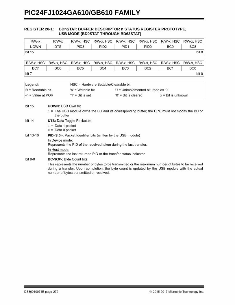
PIC24FJ1024GA610/GB610 FAMILY
REGISTER 20-1: BDnSTAT: BUFFER DESCRIPTOR n STATUS REGISTER PROTOTYPE, USB MODE (BD0STAT THROUGH BD63STAT)
R/W-x R/W-x R/W-x, HSC R/W-x, HSC R/W-x, HSC R/W-x, HSC R/W-x, HSC R/W-x, HSC
UOWN DTS PID3 PID2 PID1 PID0 BC9 BC8
bit 15 bit 8
R/W-x, HSC R/W-x, HSC R/W-x, HSC R/W-x, HSC R/W-x, HSC R/W-x, HSC R/W-x, HSC R/W-x, HSC
BC7 BC6 BC5 BC4 BC3 BC2 BC1 BC0
bit 7 bit 0
Legend: HSC = Hardware Settable/Clearable bit
R = Readable bit W = Writable bit U = Unimplemented bit, read as ‘0’
-n = Value at POR ‘1’ = Bit is set ‘0’ = Bit is cleared x = Bit is unknown
bit 15 UOWN: USB Own bit
1 = The USB module owns the BD and its corresponding buffer; the CPU must not modify the BD orthe buffer
bit 14 DTS: Data Toggle Packet bit
1 = Data 1 packet0 = Data 0 packet
bit 13-10 PID<3:0>: Packet Identifier bits (written by the USB module)
In Device mode:Represents the PID of the received token during the last transfer.
In Host mode:Represents the last returned PID or the transfer status indicator.
bit 9-0 BC<9:0>: Byte Count bits
This represents the number of bytes to be transmitted or the maximum number of bytes to be receivedduring a transfer. Upon completion, the byte count is updated by the USB module with the actualnumber of bytes transmitted or received.
DS30010074E-page 272 2015-2017 Microchip Technology Inc.

PIC24FJ1024GA610/GB610 FAMILY
REGISTER 20-2: BDnSTAT: BUFFER DESCRIPTOR n STATUS REGISTER PROTOTYPE, CPU MODE (BD0STAT THROUGH BD63STAT)
R/W-x R/W-x r-0 r-0 R/W-x R/W-x R/W-x, HSC R/W-x, HSC
UOWN DTS(1) — — DTSEN BSTALL BC9 BC8
bit 15 bit 8
R/W-x, HSC R/W-x, HSC R/W-x, HSC R/W-x, HSC R/W-x, HSC R/W-x, HSC R/W-x, HSC R/W-x, HSC
BC7 BC6 BC5 BC4 BC3 BC2 BC1 BC0
bit 7 bit 0
Legend: r = Reserved bit HSC = Hardware Settable/Clearable bit
R = Readable bit W = Writable bit U = Unimplemented bit, read as ‘0’
-n = Value at POR ‘1’ = Bit is set ‘r’ = Reserved bit x = Bit is unknown
bit 15 UOWN: USB Own bit
0 = The microcontroller core owns the BD and its corresponding buffer; the USB module ignores allother fields in the BD
bit 14 DTS: Data Toggle Packet bit(1)
1 = Data 1 packet0 = Data 0 packet
bit 13-12 Reserved: Maintain as ‘0’
bit 11 DTSEN: Data Toggle Synchronization Enable bit
1 = Data toggle synchronization is enabled; data packets with incorrect Sync value will be ignored0 = No data toggle synchronization is performed
bit 10 BSTALL: Buffer STALL Enable bit
1 = Buffer STALL is enabled; STALL handshake issued if a token is received that would use the BD inthe given location (UOWN bit remains set, BD value is unchanged); corresponding EPSTALL bitwill get set on any STALL handshake
0 = Buffer STALL is disabled
bit 9-0 BC<9:0>: Byte Count bits
This represents the number of bytes to be transmitted or the maximum number of bytes to be receivedduring a transfer. Upon completion, the byte count is updated by the USB module with the actualnumber of bytes transmitted or received.
Note 1: This bit is ignored unless DTSEN = 1.
2015-2017 Microchip Technology Inc. DS30010074E-page 273

PIC24FJ1024GA610/GB610 FAMILY
20.3 USB Interrupts
The USB OTG module has many conditions that canbe configured to cause an interrupt. All interruptsources use the same interrupt vector.
Figure 20-8 shows the interrupt logic for the USBmodule. There are two layers of interrupt registers inthe USB module. The top level consists of overall USBstatus interrupts; these are enabled and flagged in theU1IE and U1IR registers, respectively. The secondlevel consists of USB error conditions, which areenabled and flagged in the U1EIR and U1EIE registers.
An interrupt condition in any of these triggers a USBError Interrupt Flag (UERRIF) in the top level. Unlikethe device-level interrupt flags in the IFSx registers,USB interrupt flags in the U1IR registers can only becleared by writing a ‘1’ to the bit position.
Interrupts may be used to trap routine events in a USBtransaction. Figure 20-9 provides some commonevents within a USB frame and their correspondinginterrupts.
FIGURE 20-8: USB OTG INTERRUPT FUNNEL
DMAEFDMAEE
BTOEFBTOEE
DFN8EFDFN8EE
CRC16EFCRC16EE
CRC5EF (EOFEF)CRC5EE (EOFEE)
PIDEFPIDEE
ATTACHIFATTACHIE
RESUMEIFRESUMEIE
IDLEIFIDLEIE
TRNIFTRNIE
SOFIFSOFIE
URSTIF (DETACHIF)URSTIE (DETACHIE)
(UERRIF)
UERRIE
Set USB1IF
STALLIFSTALLIE
BTSEFBTSEE
T1MSECIFTIMSECIE
LSTATEIFLSTATEIE
ACTVIFACTVIE
SESVDIFSESVDIE
SESENDIFSESENDIE
VBUSVDIFVBUSVDIE
IDIFIDIE
Second Level (USB Error) Interrupts
Top Level (USB Status) Interrupts
Top Level (USB OTG) Interrupts
DS30010074E-page 274 2015-2017 Microchip Technology Inc.

PIC24FJ1024GA610/GB610 FAMILY
20.3.1 CLEARING USB OTG INTERRUPTS
Unlike device-level interrupts, the USB OTG interruptstatus flags are not freely writable in software. All USBOTG flag bits are implemented as hardware set onlybits. Additionally, these bits can only be cleared insoftware by writing a ‘1’ to their locations (i.e., perform-ing a MOV type instruction). Writing a ‘0’ to a flag bit (i.e.,a BCLR instruction) has no effect.
FIGURE 20-9: EXAMPLE OF A USB TRANSACTION AND INTERRUPT EVENTS
20.4 Device Mode Operation
The following section describes how to perform a com-mon Device mode task. In Device mode, USB transfersare performed at the transfer level. The USB moduleautomatically performs the status phase of the transfer.
20.4.1 ENABLING DEVICE MODE
1. Reset the Ping-Pong Buffer Pointers by setting,then clearing, the Ping-Pong Buffer Reset bit,PPBRST (U1CON<1>).
2. Disable all interrupts (U1IE and U1EIE = 00h).
3. Clear any existing interrupt flags by writing FFhto U1IR and U1EIR.
4. Verify that VBUS is present (non-OTG devicesonly).
5. Enable the USB module by setting the USBENbit (U1CON<0>).
6. Set the OTGEN bit (U1OTGCON<2>) to enableOTG operation.
7. Enable the Endpoint 0 buffer to receive the firstsetup packet by setting the EPRXEN andEPHSHK bits for Endpoint 0 (U1EP0<3,0> = 1).
8. Power up the USB module by setting theUSBPWR bit (U1PWRC<0>).
9. Enable the D+ pull-up resistor to signal an attachby setting the DPPULUP bit (U1OTGCON<7>).
Note: Throughout this data sheet, a bit that canonly be cleared by writing a ‘1’ to its loca-tion is referred to as “Write ‘1’ to Clear”. Inregister descriptions; this function isindicated by the descriptor, “K”.
USB Reset
SOFRESET SETUP DATA STATUS SOF
SETUP Token Data ACK
OUT Token Empty Data ACK
Start-of-Frame (SOF)IN Token Data ACK
SOFIF
URSTIF
1 ms Frame
Differential Data
From Host From Host To Host
From Host To Host From Host
From Host From Host To Host
Transaction
Control Transfer(1)
TransactionComplete
Note 1: The control transfer shown here is only an example showing events that can occur for every transaction. Typical control transfers will spread across multiple frames.
Set TRNIF
Set TRNIF
Set TRNIF
2015-2017 Microchip Technology Inc. DS30010074E-page 275

PIC24FJ1024GA610/GB610 FAMILY
20.4.2 RECEIVING AN IN TOKEN IN DEVICE MODE
1. Attach to a USB host and enumerate as describedin Chapter 9 of the “USB 2.0 Specification”.
2. Create a data buffer and populate it with the datato send to the host.
3. In the appropriate (even or odd) TX BD for thedesired endpoint:
a) Set up the status register (BDnSTAT) withthe correct data toggle (DATA0/1) value andthe byte count of the data buffer.
b) Set up the address register (BDnADR) withthe starting address of the data buffer.
c) Set the UOWN bit of the status register to‘1’.
4. When the USB module receives an IN token, itautomatically transmits the data in the buffer.Upon completion, the module updates thestatus register (BDnSTAT) and sets the TokenComplete Interrupt Flag, TRNIF (U1IR<3>).
20.4.3 RECEIVING AN OUT TOKEN IN DEVICE MODE
1. Attach to a USB host and enumerate asdescribed in Chapter 9 of the “USB 2.0Specification”.
2. Create a data buffer with the amount of data youare expecting from the host.
3. In the appropriate (even or odd) TX BD for thedesired endpoint:
a) Set up the status register (BDnSTAT) withthe correct data toggle (DATA0/1) value andthe byte count of the data buffer.
b) Set up the address register (BDnADR) withthe starting address of the data buffer.
c) Set the UOWN bit of the status register to‘1’.
4. When the USB module receives an OUT token,it automatically receives the data sent by thehost to the buffer. Upon completion, the moduleupdates the status register (BDnSTAT) and setsthe Token Complete Interrupt Flag, TRNIF(U1IR<3>).
20.5 Host Mode Operation
The following sections describe how to perform commonHost mode tasks. In Host mode, USB transfers areinvoked explicitly by the host software. The hostsoftware is responsible for the Acknowledge portion ofthe transfer. Also, all transfers are performed using theEndpoint 0 Control register (U1EP0) and BufferDescriptors.
20.5.1 ENABLE HOST MODE AND DISCOVER A CONNECTED DEVICE
1. Enable Host mode by setting the HOSTEN bit(U1CON<3>). This causes the Host mode con-trol bits in other USB OTG registers to becomeavailable.
2. Enable the D+ and D- pull-down resistors bysetting the DPPULDWN and DMPULDWN bits(U1OTGCON<5:4>). Disable the D+ and D-pull-up resistors by clearing the DPPULUP andDMPULUP bits (U1OTGCON<7:6>).
3. At this point, SOF generation begins with theSOF counter loaded with 12,000. Eliminatenoise on the USB by clearing the SOFEN bit(U1CON<0>) to disable Start-of-Frame (SOF)packet generation.
4. Enable the device attached interrupt by settingthe ATTACHIE bit (U1IE<6>).
5. Wait for the device attached interrupt(U1IR<6> = 1). This is signaled by the USBdevice changing the state of D+ or D- from ‘0’to ‘1’ (SE0 to J-state). After it occurs, wait100 ms for the device power to stabilize.
6. Check the state of the JSTATE and SE0 bits inU1CON. If the JSTATE bit (U1CON<7>) is ‘0’,the connecting device is low speed. If the con-necting device is low speed, set the LSPDENand LSPD bits (U1ADDR<7> and U1EP0<7>) toenable low-speed operation.
7. Reset the USB device by setting the USBRSTbit (U1CON<4>) for at least 50 ms, sendingReset signaling on the bus. After 50 ms,terminate the Reset by clearing USBRST.
8. In order to keep the connected device fromgoing into suspend, enable the SOF packetgeneration by setting the SOFEN bit.
9. Wait 10 ms for the device to recover from Reset.
10. Perform enumeration as described by Chapter 9of the “USB 2.0 Specification”.
DS30010074E-page 276 2015-2017 Microchip Technology Inc.
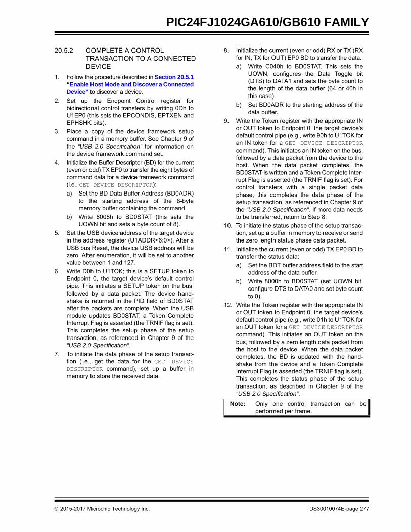
PIC24FJ1024GA610/GB610 FAMILY
20.5.2 COMPLETE A CONTROL TRANSACTION TO A CONNECTED DEVICE
1. Follow the procedure described in Section 20.5.1“Enable Host Mode and Discover a ConnectedDevice” to discover a device.
2. Set up the Endpoint Control register forbidirectional control transfers by writing 0Dh toU1EP0 (this sets the EPCONDIS, EPTXEN andEPHSHK bits).
3. Place a copy of the device framework setupcommand in a memory buffer. See Chapter 9 ofthe “USB 2.0 Specification” for information onthe device framework command set.
4. Initialize the Buffer Descriptor (BD) for the current(even or odd) TX EP0 to transfer the eight bytes ofcommand data for a device framework command(i.e., GET DEVICE DESCRIPTOR):
a) Set the BD Data Buffer Address (BD0ADR)to the starting address of the 8-bytememory buffer containing the command.
b) Write 8008h to BD0STAT (this sets theUOWN bit and sets a byte count of 8).
5. Set the USB device address of the target devicein the address register (U1ADDR<6:0>). After aUSB bus Reset, the device USB address will bezero. After enumeration, it will be set to anothervalue between 1 and 127.
6. Write D0h to U1TOK; this is a SETUP token toEndpoint 0, the target device’s default controlpipe. This initiates a SETUP token on the bus,followed by a data packet. The device hand-shake is returned in the PID field of BD0STATafter the packets are complete. When the USBmodule updates BD0STAT, a Token CompleteInterrupt Flag is asserted (the TRNIF flag is set).This completes the setup phase of the setuptransaction, as referenced in Chapter 9 of the“USB 2.0 Specification”.
7. To initiate the data phase of the setup transac-tion (i.e., get the data for the GET DEVICEDESCRIPTOR command), set up a buffer inmemory to store the received data.
8. Initialize the current (even or odd) RX or TX (RXfor IN, TX for OUT) EP0 BD to transfer the data.
a) Write C040h to BD0STAT. This sets theUOWN, configures the Data Toggle bit(DTS) to DATA1 and sets the byte count tothe length of the data buffer (64 or 40h inthis case).
b) Set BD0ADR to the starting address of thedata buffer.
9. Write the Token register with the appropriate INor OUT token to Endpoint 0, the target device’sdefault control pipe (e.g., write 90h to U1TOK foran IN token for a GET DEVICE DESCRIPTORcommand). This initiates an IN token on the bus,followed by a data packet from the device to thehost. When the data packet completes, theBD0STAT is written and a Token Complete Inter-rupt Flag is asserted (the TRNIF flag is set). Forcontrol transfers with a single packet dataphase, this completes the data phase of thesetup transaction, as referenced in Chapter 9 ofthe “USB 2.0 Specification”. If more data needsto be transferred, return to Step 8.
10. To initiate the status phase of the setup transac-tion, set up a buffer in memory to receive or sendthe zero length status phase data packet.
11. Initialize the current (even or odd) TX EP0 BD totransfer the status data:
a) Set the BDT buffer address field to the startaddress of the data buffer.
b) Write 8000h to BD0STAT (set UOWN bit,configure DTS to DATA0 and set byte countto 0).
12. Write the Token register with the appropriate INor OUT token to Endpoint 0, the target device’sdefault control pipe (e.g., write 01h to U1TOK foran OUT token for a GET DEVICE DESCRIPTORcommand). This initiates an OUT token on thebus, followed by a zero length data packet fromthe host to the device. When the data packetcompletes, the BD is updated with the hand-shake from the device and a Token CompleteInterrupt Flag is asserted (the TRNIF flag is set).This completes the status phase of the setuptransaction, as described in Chapter 9 of the“USB 2.0 Specification”.
Note: Only one control transaction can beperformed per frame.
2015-2017 Microchip Technology Inc. DS30010074E-page 277

PIC24FJ1024GA610/GB610 FAMILY
20.5.3 SEND A FULL-SPEED BULK DATA TRANSFER TO A TARGET DEVICE
1. Follow the procedure described in Section 20.5.1“Enable Host Mode and Discover a ConnectedDevice” and Section 20.5.2 “Complete a Con-trol Transaction to a Connected Device” todiscover and configure a device.
2. To enable transmit and receive transfers withhandshaking enabled, write 1Dh to U1EP0. Ifthe target device is a low-speed device, also setthe LSPD (U1EP0<7>) bit. If you want the hard-ware to automatically retry indefinitely if thetarget device asserts a NAK on the transfer,clear the Retry Disable bit, RETRYDIS(U1EP0<6>).
3. Set up the BD for the current (even or odd) TXEP0 to transfer up to 64 bytes.
4. Set the USB device address of the target devicein the address register (U1ADDR<6:0>).
5. Write an OUT token to the desired endpoint toU1TOK. This triggers the module’s transmitstate machines to begin transmitting the tokenand the data.
6. Wait for the Token Complete Interrupt Flag,TRNIF. This indicates that the BD has beenreleased back to the microprocessor and thetransfer has completed. If the Retry Disable bit(RETRYDIS) is set, the handshake (ACK, NAK,STALL or ERROR (0Fh)) is returned in the BDPID field. If a STALL interrupt occurs, thepending packet must be dequeued and the errorcondition in the target device cleared. If a detachinterrupt occurs (SE0 for more than 2.5 µs), thenthe target has detached (U1IR<0> is set).
7. Once the Token Complete Interrupt Flag occurs(TRNIF is set), the BD can be examined and thenext data packet queued by returning to Step 2.
20.6 OTG Operation
20.6.1 SESSION REQUEST PROTOCOL (SRP)
An OTG A-device may decide to power down the VBUS
supply when it is not using the USB link through theSession Request Protocol (SRP). SRP can only be initi-ated at full speed. Software may do this by configuring aGPIO pin to disable an external power transistor, or volt-age regulator enable signal, which controls the VBUS
supply. When the VBUS supply is powered down, theA-device is said to have ended a USB session.
An OTG A-device or embedded host may repower theVBUS supply at any time (initiate a new session). AnOTG B-device may also request that the OTG A-devicerepower the VBUS supply (initiate a new session). Thisis accomplished via Session Request Protocol (SRP).
Prior to requesting a new session, the B-device must firstcheck that the previous session has definitely ended. Todo this, the B-device must check for two conditions:
1. VBUS supply is below the session valid voltage.
2. Both D+ and D- have been low for at least 2 ms.
The B-device will be notified of Condition 1 by theSESENDIF (U1OTGIR<2>) interrupt. Software willhave to manually check for Condition 2.
The B-device may aid in achieving Condition 1 by dis-charging the VBUS supply through a resistor. Softwaremay do this by setting VBUSDIS (U1OTGCON<0>).
After these initial conditions are met, the B-device maybegin requesting the new session. The B-device beginsby pulsing the D+ data line. Software should do this bysetting DPPULUP (U1OTGCON<7>). The data lineshould be held high for 5 to 10 ms.
The B-device then proceeds by pulsing the VBUS
supply. Software should do this by setting PUVBUS(U1CNFG2<4>). When an A-device detects SRPsignaling (either via the ATTACHIF (U1IR<6>) interruptor via the SESVDIF (U1OTGIR<3>) interrupt), theA-device must restore the VBUS supply by properlyconfiguring the general purpose I/O port pin controllingthe external power source.
The B-device should not monitor the state of the VBUS
supply while performing VBUS supply pulsing. When theB-device does detect that the VBUS supply has beenrestored (via the SESVDIF (U1OTGIR<3>) interrupt),the B-device must reconnect to the USB link by pullingup D+ or D- (via the DPPULUP or DMPULUP bit).
The A-device must complete the SRP by driving USBReset signaling.
Note: USB speed, transceiver and pull-upsshould only be configured during themodule setup phase. It is not recom-mended to change these settings whilethe module is enabled.
Note: When the A-device powers down theVBUS supply, the B-device must discon-nect its pull-up resistor from power. If thedevice is self-powered, it can do this byclearing DPPULUP (U1OTGCON<7>) andDMPULUP (U1OTGCON<6>).
DS30010074E-page 278 2015-2017 Microchip Technology Inc.

PIC24FJ1024GA610/GB610 FAMILY
20.6.2 HOST NEGOTIATION PROTOCOL (HNP)
In USB OTG applications, a Dual Role Device (DRD) isa device that is capable of being either a host or aperipheral. Any OTG DRD must support HostNegotiation Protocol (HNP).
HNP allows an OTG B-device to temporarily become theUSB host. The A-device must first enable the B-deviceto follow HNP. Refer to the “On-The-Go Supplement” tothe “USB 2.0 Specification” for more informationregarding HNP. HNP may only be initiated at full speed.
After being enabled for HNP by the A-device, theB-device requests being the host any time that the USBlink is in the suspend state, by simply indicating a dis-connect. This can be done in software by clearingDPPULUP and DMPULUP. When the A-device detectsthe disconnect condition (via the URSTIF (U1IR<0>)interrupt), the A-device may allow the B-device to takeover as host. The A-device does this by signaling con-nect as a full-speed function. Software may accomplishthis by setting DPPULUP.
If the A-device responds instead with resume signaling,the A-device remains as host. When the B-devicedetects the connect condition (via ATTACHIF,U1IR<6>), the B-device becomes host. The B-devicedrives Reset signaling prior to using the bus.
When the B-device has finished in its role as host, itstops all bus activity and turns on its D+ pull-up resistorby setting DPPULUP. When the A-device detects asuspend condition (Idle for 3 ms), the A-device turns offits D+ pull-up. The A-device may also power down theVBUS supply to end the session. When the A-devicedetects the connect condition (via ATTACHIF), theA-device resumes host operation and drives Resetsignaling.
20.7 USB OTG Module Registers
There are a total of 37 memory-mapped registers asso-ciated with the USB OTG module. They can be dividedinto four general categories:
• USB OTG Module Control (12)
• USB Interrupt (7)
• USB Endpoint Management (16)
• USB VBUS Power Control (2)
This total does not include the (up to) 128 BD registersin the BDT. Their prototypes, described inRegister 20-1 and Register 20-2, are shown sepa-rately in Section 20.2 “USB Buffer Descriptors andthe BDT”.
All USB OTG registers are implemented in the LeastSignificant Byte (LSB) of the register. Bits in the upperbyte are unimplemented and have no function. Notethat some registers are instantiated only in Host mode,while other registers have different bit instantiationsand functions in Device and Host modes.
The registers described in the following sections arethose that have bits with specific control and configura-tion features. The following registers are used for dataor address values only:
• U1BDTP1, U1BDTP2 and U1BDTP3: Specifies the 256-word page in data RAM used for the BDT; 8-bit value with bit 0 fixed as ‘0’ for boundary alignment.
• U1FRML and U1FRMH: Contains the 11-bit byte counter for the current data frame.
2015-2017 Microchip Technology Inc. DS30010074E-page 279

PIC24FJ1024GA610/GB610 FAMILY
20.7.1 USB OTG MODULE CONTROL REGISTERS
REGISTER 20-3: U1OTGSTAT: USB OTG STATUS REGISTER (HOST MODE ONLY)
U-0 U-0 U-0 U-0 U-0 U-0 U-0 U-0
— — — — — — — —
bit 15 bit 8
R-0, HSC U-0 R-0, HSC U-0 R-0, HSC R-0, HSC U-0 R-0, HSC
ID — LSTATE — SESVD SESEND — VBUSVD
bit 7 bit 0
Legend: U = Unimplemented bit, read as ‘0’
R = Readable bit W = Writable bit HSC = Hardware Settable/Clearable bit
-n = Value at POR ‘1’ = Bit is set ‘0’ = Bit is cleared x = Bit is unknown
bit 15-8 Unimplemented: Read as ‘0’
bit 7 ID: ID Pin State Indicator bit
1 = No plug is attached or a Type B cable has been plugged into the USB receptacle0 = A Type A plug has been plugged into the USB receptacle
bit 6 Unimplemented: Read as ‘0’
bit 5 LSTATE: Line State Stable Indicator bit
1 = The USB line state (as defined by SE0 and JSTATE) has been stable for the previous 1 ms0 = The USB line state has not been stable for the previous 1 ms
bit 4 Unimplemented: Read as ‘0’
bit 3 SESVD: Session Valid Indicator bit
1 = The VBUS voltage is above VA_SESS_VLD (as defined in the “USB 2.0 Specification”) on the A orB-device
0 = The VBUS voltage is below VA_SESS_VLD on the A or B-device
bit 2 SESEND: B Session End Indicator bit
1 = The VBUS voltage is below VB_SESS_END (as defined in the “USB 2.0 Specification”) on theB-device
0 = The VBUS voltage is above VB_SESS_END on the B-device
bit 1 Unimplemented: Read as ‘0’
bit 0 VBUSVD: A VBUS Valid Indicator bit
1 = The VBUS voltage is above VA_VBUS_VLD (as defined in the “USB 2.0 Specification”) on theA-device
0 = The VBUS voltage is below VA_VBUS_VLD on the A-device
DS30010074E-page 280 2015-2017 Microchip Technology Inc.

PIC24FJ1024GA610/GB610 FAMILY
REGISTER 20-4: U1OTGCON: USB ON-THE-GO CONTROL REGISTER
U-0 U-0 U-0 U-0 U-0 U-0 U-0 U-0
— — — — — — — —
bit 15 bit 8
R/W-0 R/W-0 R/W-0 R/W-0 r-0 R/W-0 r-0 R/W-0
DPPULUP DMPULUP DPPULDWN(1) DMPULDWN(1) — OTGEN(1) — VBUSDIS(1)
bit 7 bit 0
Legend: r = Reserved bit
R = Readable bit W = Writable bit U = Unimplemented bit, read as ‘0’
-n = Value at POR ‘1’ = Bit is set ‘0’ = Bit is cleared x = Bit is unknown
bit 15-8 Unimplemented: Read as ‘0’
bit 7 DPPULUP: D+ Pull-up Enable bit
1 = D+ data line pull-up resistor is enabled0 = D+ data line pull-up resistor is disabled
bit 6 DMPULUP: D- Pull-up Enable bit
1 = D- data line pull-up resistor is enabled0 = D- data line pull-up resistor is disabled
bit 5 DPPULDWN: D+ Pull-Down Enable bit(1)
1 = D+ data line pull-down resistor is enabled0 = D+ data line pull-down resistor is disabled
bit 4 DMPULDWN: D- Pull-Down Enable bit(1)
1 = D- data line pull-down resistor is enabled0 = D- data line pull-down resistor is disabled
bit 3 Reserved: Maintain as ‘0’
bit 2 OTGEN: OTG Features Enable bit(1)
1 = USB OTG is enabled; all D+/D- pull-up and pull-down bits are enabled0 = USB OTG is disabled; D+/D- pull-up and pull-down bits are controlled in hardware by the settings
of the HOSTEN and USBEN (U1CON<3,0>) bits
bit 1 Reserved: Maintain as ‘0’
bit 0 VBUSDIS: VBUS Discharge Enable bit(1)
1 = VBUS line is discharged through a resistor0 = VBUS line is not discharged
Note 1: These bits are only used in Host mode; do not use in Device mode.
2015-2017 Microchip Technology Inc. DS30010074E-page 281

PIC24FJ1024GA610/GB610 FAMILY
REGISTER 20-5: U1PWRC: USB POWER CONTROL REGISTER
U-0 U-0 U-0 U-0 U-0 U-0 U-0 U-0
— — — — — — — —
bit 15 bit 8
R-x, HSC U-0 U-0 R/W-0 U-0 U-0 R/W-0, HC R/W-0
UACTPND — — USLPGRD — — USUSPND USBPWR
bit 7 bit 0
Legend: HC = Hardware Clearable bit HSC = Hardware Settable/Clearable bit
R = Readable bit W = Writable bit U = Unimplemented bit, read as ‘0’
-n = Value at POR ‘1’ = Bit is set ‘0’ = Bit is cleared x = Bit is unknown
bit 15-8 Unimplemented: Read as ‘0’
bit 7 UACTPND: USB Activity Pending bit
1 = Module should not be suspended at the moment (requires the USLPGRD bit to be set)0 = Module may be suspended or powered down
bit 6-5 Unimplemented: Read as ‘0’
bit 4 USLPGRD: USB Sleep/Suspend Guard bit
1 = Indicates to the USB module that it is about to be suspended or powered down0 = No suspend
bit 3-2 Unimplemented: Read as ‘0’
bit 1 USUSPND: USB Suspend Mode Enable bit
1 = USB OTG module is in Suspend mode; USB clock is gated and the transceiver is placed in alow-power state
0 = Normal USB OTG operation
bit 0 USBPWR: USB Operation Enable bit
1 = USB OTG module is enabled0 = USB OTG module is disabled(1)
Note 1: Do not clear this bit unless the HOSTEN, USBEN and OTGEN bits (U1CON<3,0> and U1OTGCON<2>) are all cleared.
DS30010074E-page 282 2015-2017 Microchip Technology Inc.

PIC24FJ1024GA610/GB610 FAMILY
REGISTER 20-6: U1STAT: USB STATUS REGISTER
U-0 U-0 U-0 U-0 U-0 U-0 U-0 U-0
— — — — — — — —
bit 15 bit 8
R-0, HSC R-0, HSC R-0, HSC R-0, HSC R-0, HSC R-0, HSC U-0 U-0
ENDPT3 ENDPT2 ENDPT1 ENDPT0 DIR PPBI(1) — —
bit 7 bit 0
Legend: U = Unimplemented bit, read as ‘0’
R = Readable bit W = Writable bit HSC = Hardware Settable/Clearable bit
-n = Value at POR ‘1’ = Bit is set ‘0’ = Bit is cleared x = Bit is unknown
bit 15-8 Unimplemented: Read as ‘0’
bit 7-4 ENDPT<3:0>: Number of the Last Endpoint Activity bits (Represents the number of the BDT updated by the last USB transfer.)
1111 = Endpoint 151110 = Endpoint 14•••0001 = Endpoint 10000 = Endpoint 0
bit 3 DIR: Last BD Direction Indicator bit
1 = The last transaction was a transmit transfer (TX)0 = The last transaction was a receive transfer (RX)
bit 2 PPBI: Ping-Pong BD Pointer Indicator bit(1)
1 = The last transaction was to the odd BD bank0 = The last transaction was to the even BD bank
bit 1-0 Unimplemented: Read as ‘0’
Note 1: This bit is only valid for endpoints with available even and odd BD registers.
2015-2017 Microchip Technology Inc. DS30010074E-page 283
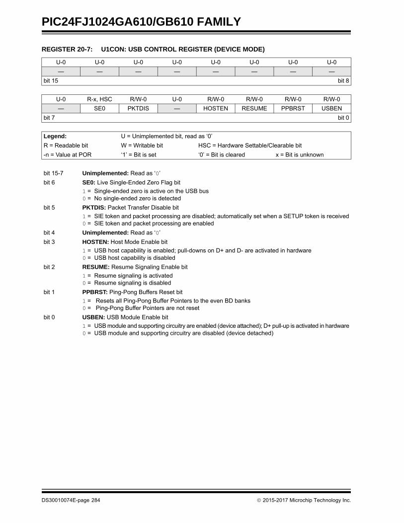
PIC24FJ1024GA610/GB610 FAMILY
REGISTER 20-7: U1CON: USB CONTROL REGISTER (DEVICE MODE)
U-0 U-0 U-0 U-0 U-0 U-0 U-0 U-0
— — — — — — — —
bit 15 bit 8
U-0 R-x, HSC R/W-0 U-0 R/W-0 R/W-0 R/W-0 R/W-0
— SE0 PKTDIS — HOSTEN RESUME PPBRST USBEN
bit 7 bit 0
Legend: U = Unimplemented bit, read as ‘0’
R = Readable bit W = Writable bit HSC = Hardware Settable/Clearable bit
-n = Value at POR ‘1’ = Bit is set ‘0’ = Bit is cleared x = Bit is unknown
bit 15-7 Unimplemented: Read as ‘0’
bit 6 SE0: Live Single-Ended Zero Flag bit
1 = Single-ended zero is active on the USB bus0 = No single-ended zero is detected
bit 5 PKTDIS: Packet Transfer Disable bit
1 = SIE token and packet processing are disabled; automatically set when a SETUP token is received0 = SIE token and packet processing are enabled
bit 4 Unimplemented: Read as ‘0’
bit 3 HOSTEN: Host Mode Enable bit
1 = USB host capability is enabled; pull-downs on D+ and D- are activated in hardware 0 = USB host capability is disabled
bit 2 RESUME: Resume Signaling Enable bit
1 = Resume signaling is activated0 = Resume signaling is disabled
bit 1 PPBRST: Ping-Pong Buffers Reset bit
1 = Resets all Ping-Pong Buffer Pointers to the even BD banks0 = Ping-Pong Buffer Pointers are not reset
bit 0 USBEN: USB Module Enable bit
1 = USB module and supporting circuitry are enabled (device attached); D+ pull-up is activated in hardware0 = USB module and supporting circuitry are disabled (device detached)
DS30010074E-page 284 2015-2017 Microchip Technology Inc.

PIC24FJ1024GA610/GB610 FAMILY
REGISTER 20-8: U1CON: USB CONTROL REGISTER (HOST MODE ONLY)
U-0 U-0 U-0 U-0 U-0 U-0 U-0 U-0
— — — — — — — —
bit 15 bit 8
R-x, HSC R-x, HSC R/W-0 R/W-0 R/W-0 R/W-0 R/W-0 R/W-0
JSTATE SE0 TOKBUSY USBRST HOSTEN RESUME PPBRST SOFEN
bit 7 bit 0
Legend: U = Unimplemented bit, read as ‘0’
R = Readable bit W = Writable bit HSC = Hardware Settable/Clearable bit
-n = Value at POR ‘1’ = Bit is set ‘0’ = Bit is cleared x = Bit is unknown
bit 15-8 Unimplemented: Read as ‘0’
bit 7 JSTATE: Live Differential Receiver J-State Flag bit
1 = J-state (differential ‘0’ in low speed, differential ‘1’ in full speed) is detected on the USB0 = No J-state is detected
bit 6 SE0: Live Single-Ended Zero Flag bit
1 = Single-ended zero is active on the USB bus0 = No single-ended zero is detected
bit 5 TOKBUSY: Token Busy Status bit
1 = Token is being executed by the USB module in On-The-Go state0 = No token is being executed
bit 4 USBRST: USB Module Reset bit
1 = USB Reset has been generated for a software Reset; application must set this bit for 50 ms, thenclear it
0 = USB Reset is terminated
bit 3 HOSTEN: Host Mode Enable bit
1 = USB host capability is enabled; pull-downs on D+ and D- are activated in hardware 0 = USB host capability is disabled
bit 2 RESUME: Resume Signaling Enable bit
1 = Resume signaling is activated; software must set bit for 10 ms and then clear to enable remote wake-up0 = Resume signaling is disabled
bit 1 PPBRST: Ping-Pong Buffers Reset bit
1 = Resets all Ping-Pong Buffer Pointers to the even BD banks0 = Ping-Pong Buffer Pointers are not reset
bit 0 SOFEN: Start-of-Frame Enable bit
1 = Start-of-Frame token is sent every one 1 ms0 = Start-of-Frame token is disabled
2015-2017 Microchip Technology Inc. DS30010074E-page 285

PIC24FJ1024GA610/GB610 FAMILY
REGISTER 20-9: U1ADDR: USB ADDRESS REGISTER
U-0 U-0 U-0 U-0 U-0 U-0 U-0 U-0
— — — — — — — —
bit 15 bit 8
R/W-0 R/W-0 R/W-0 R/W-0 R/W-0 R/W-0 R/W-0 R/W-0
LSPDEN(1) DEVADDR6 DEVADDR5 DEVADDR4 DEVADDR3 DEVADDR2 DEVADDR1 DEVADDR0
bit 7 bit 0
Legend:
R = Readable bit W = Writable bit U = Unimplemented bit, read as ‘0’
-n = Value at POR ‘1’ = Bit is set ‘0’ = Bit is cleared x = Bit is unknown
bit 15-8 Unimplemented: Read as ‘0’
bit 7 LSPDEN: Low-Speed Enable Indicator bit(1)
1 = USB module operates at low speed0 = USB module operates at full speed
bit 6-0 DEVADDR<6:0>: USB Device Address bits
Note 1: Host mode only. In Device mode, this bit is unimplemented and read as ‘0’.
REGISTER 20-10: U1TOK: USB TOKEN REGISTER (HOST MODE ONLY)
U-0 U-0 U-0 U-0 U-0 U-0 U-0 U-0
— — — — — — — —
bit 15 bit 8
R/W-0 R/W-0 R/W-0 R/W-0 R/W-0 R/W-0 R/W-0 R/W-0
PID3 PID2 PID1 PID0 EP3 EP2 EP1 EP0
bit 7 bit 0
Legend:
R = Readable bit W = Writable bit U = Unimplemented bit, read as ‘0’
-n = Value at POR ‘1’ = Bit is set ‘0’ = Bit is cleared x = Bit is unknown
bit 15-8 Unimplemented: Read as ‘0’
bit 7-4 PID<3:0>: Token Type Identifier bits
1101 = SETUP (TX) token type transaction(1)
1001 = IN (RX) token type transaction(1)
0001 = OUT (TX) token type transaction(1)
bit 3-0 EP<3:0>: Token Command Endpoint Address bits
This value must specify a valid endpoint on the attached device.
Note 1: All other combinations are reserved and are not to be used.
DS30010074E-page 286 2015-2017 Microchip Technology Inc.

PIC24FJ1024GA610/GB610 FAMILY
REGISTER 20-11: U1SOF: USB OTG START-OF-TOKEN THRESHOLD REGISTER (HOST MODE ONLY)
U-0 U-0 U-0 U-0 U-0 U-0 U-0 U-0
— — — — — — — —
bit 15 bit 8
R/W-0 R/W-0 R/W-0 R/W-0 R/W-0 R/W-0 R/W-0 R/W-0
CNT<7:0>
bit 7 bit 0
Legend:
R = Readable bit W = Writable bit U = Unimplemented bit, read as ‘0’
-n = Value at POR ‘1’ = Bit is set ‘0’ = Bit is cleared x = Bit is unknown
bit 15-8 Unimplemented: Read as ‘0’
bit 7-0 CNT<7:0>: Start-of-Frame Size bits
Value represents 10 + (packet size of n bytes). For example:0100 1010 = 64-byte packet0010 1010 = 32-byte packet0001 0010 = 8-byte packet
2015-2017 Microchip Technology Inc. DS30010074E-page 287

PIC24FJ1024GA610/GB610 FAMILY
REGISTER 20-12: U1CNFG1: USB CONFIGURATION REGISTER 1
U-0 U-0 U-0 U-0 U-0 U-0 U-0 U-0
— — — — — — — —
bit 15 bit 8
R/W-0 R/W-0 U-0 R/W-0 U-0 U-0 R/W-0 R/W-0
UTEYE UOEMON(1) — USBSIDL — — PPB1 PPB0
bit 7 bit 0
Legend:
R = Readable bit W = Writable bit U = Unimplemented bit, read as ‘0’
-n = Value at POR ‘1’ = Bit is set ‘0’ = Bit is cleared x = Bit is unknown
bit 15-8 Unimplemented: Read as ‘0’
bit 7 UTEYE: USB Eye Pattern Test Enable bit
1 = Eye pattern test is enabled0 = Eye pattern test is disabled
bit 6 UOEMON: USB OE Monitor Enable bit(1)
1 = OE signal is active; it indicates intervals during which the D+/D- lines are driving0 = OE signal is inactive
bit 5 Unimplemented: Read as ‘0’
bit 4 USBSIDL: USB OTG Stop in Idle Mode bit
1 = Discontinues module operation when the device enters Idle mode0 = Continues module operation in Idle mode
bit 3-2 Unimplemented: Read as ‘0’
bit 1-0 PPB<1:0>: Ping-Pong Buffers Configuration bits
11 = Even/Odd Ping-Pong Buffers are enabled for Endpoints 1 to 1510 = Even/Odd Ping-Pong Buffers are enabled for all endpoints01 = Even/Odd Ping-Pong Buffers are enabled for RX Endpoint 000 = Even/Odd Ping-Pong Buffers are disabled
Note 1: This bit is only active when the UTRDIS bit (U1CNFG2<0>) is set.
DS30010074E-page 288 2015-2017 Microchip Technology Inc.

PIC24FJ1024GA610/GB610 FAMILY
REGISTER 20-13: U1CNFG2: USB CONFIGURATION REGISTER 2
U-0 U-0 U-0 U-0 U-0 U-0 U-0 U-0
— — — — — — — —
bit 15 bit 8
U-0 U-0 U-0 R/W-0 R/W-0 U-0 U-0 U-0
— — — PUVBUS EXTI2CEN — — —
bit 7 bit 0
Legend:
R = Readable bit W = Writable bit U = Unimplemented bit, read as ‘0’
-n = Value at POR ‘1’ = Bit is set ‘0’ = Bit is cleared x = Bit is unknown
bit 15-5 Unimplemented: Read as ‘0’
bit 4 PUVBUS: VBUS Pull-Up Enable bit
1 = Pull-up on VBUS pin is enabled0 = Pull-up on VBUS pin is disabled
bit 3 EXTI2CEN: I2C Interface for External Module Control Enable bit
1 = External module(s) is controlled via the I2C interface0 = External module(s) is controlled via the dedicated pins
bit 2-0 Unimplemented: Read as ‘0’
2015-2017 Microchip Technology Inc. DS30010074E-page 289

PIC24FJ1024GA610/GB610 FAMILY
20.7.2 USB INTERRUPT REGISTERS
REGISTER 20-14: U1OTGIR: USB OTG INTERRUPT STATUS REGISTER (HOST MODE ONLY)
U-0 U-0 U-0 U-0 U-0 U-0 U-0 U-0
— — — — — — — —
bit 15 bit 8
R/K-0, HS R/K-0, HS R/K-0, HS R/K-0, HS R/K-0, HS R/K-0, HS U-0 R/K-0, HS
IDIF T1MSECIF LSTATEIF ACTVIF SESVDIF SESENDIF — VBUSVDIF
bit 7 bit 0
Legend: HS = Hardware Settable bit
R = Readable bit K = Write ‘1’ to Clear bit U = Unimplemented bit, read as ‘0’
-n = Value at POR ‘1’ = Bit is set ‘0’ = Bit is cleared x = Bit is unknown
bit 15-8 Unimplemented: Read as ‘0’
bit 7 IDIF: ID State Change Indicator bit
1 = Change in ID state is detected0 = No ID state change is detected
bit 6 T1MSECIF: 1 Millisecond Timer bit
1 = The 1 millisecond timer has expired0 = The 1 millisecond timer has not expired
bit 5 LSTATEIF: Line State Stable Indicator bit
1 = USB line state (as defined by the SE0 and JSTATE bits) has been stable for 1 ms, but different fromthe last time
0 = USB line state has not been stable for 1 ms
bit 4 ACTVIF: Bus Activity Indicator bit
1 = Activity on the D+/D- lines or VBUS is detected0 = No activity on the D+/D- lines or VBUS is detected
bit 3 SESVDIF: Session Valid Change Indicator bit
1 = VBUS has crossed VA_SESS_END (as defined in the “USB 2.0 Specification”)(1)
0 = VBUS has not crossed VA_SESS_END
bit 2 SESENDIF: B-Device VBUS Change Indicator bit
1 = VBUS change on B-device is detected; VBUS has crossed VB_SESS_END (as defined in the “USB 2.0Specification”)(1)
0 = VBUS has not crossed VB_SESS_END
bit 1 Unimplemented: Read as ‘0’
bit 0 VBUSVDIF: A-Device VBUS Change Indicator bit
1 = VBUS change on A-device is detected; VBUS has crossed VA_VBUS_VLD (as defined in the “USB 2.0Specification”)(1)
0 = No VBUS change on A-device is detected
Note 1: VBUS threshold crossings may either be rising or falling.
Note: Individual bits can only be cleared by writing a ‘1’ to the bit position as part of a word write operation on theentire register. Using Boolean instructions or bitwise operations to write to a single bit position will causeall set bits, at the moment of the write, to become cleared.
DS30010074E-page 290 2015-2017 Microchip Technology Inc.

PIC24FJ1024GA610/GB610 FAMILY
REGISTER 20-15: U1OTGIE: USB OTG INTERRUPT ENABLE REGISTER (HOST MODE ONLY)
U-0 U-0 U-0 U-0 U-0 U-0 U-0 U-0
— — — — — — — —
bit 15 bit 8
R/W-0 R/W-0 R/W-0 R/W-0 R/W-0 R/W-0 U-0 R/W-0
IDIE T1MSECIE LSTATEIE ACTVIE SESVDIE SESENDIE — VBUSVDIE
bit 7 bit 0
Legend:
R = Readable bit W = Writable bit U = Unimplemented bit, read as ‘0’
-n = Value at POR ‘1’ = Bit is set ‘0’ = Bit is cleared x = Bit is unknown
bit 15-8 Unimplemented: Read as ‘0’
bit 7 IDIE: ID Interrupt Enable bit
1 = Interrupt is enabled0 = Interrupt is disabled
bit 6 T1MSECIE: 1 Millisecond Timer Interrupt Enable bit
1 = Interrupt is enabled0 = Interrupt is disabled
bit 5 LSTATEIE: Line State Stable Interrupt Enable bit
1 = Interrupt is enabled0 = Interrupt is disabled
bit 4 ACTVIE: Bus Activity Interrupt Enable bit
1 = Interrupt is enabled0 = Interrupt is disabled
bit 3 SESVDIE: Session Valid Interrupt Enable bit
1 = Interrupt is enabled0 = Interrupt is disabled
bit 2 SESENDIE: B-Device Session End Interrupt Enable bit
1 = Interrupt is enabled0 = Interrupt is disabled
bit 1 Unimplemented: Read as ‘0’
bit 0 VBUSVDIE: A-Device VBUS Valid Interrupt Enable bit
1 = Interrupt is enabled0 = Interrupt is disabled
2015-2017 Microchip Technology Inc. DS30010074E-page 291

PIC24FJ1024GA610/GB610 FAMILY
REGISTER 20-16: U1IR: USB INTERRUPT STATUS REGISTER (DEVICE MODE ONLY)
U-0 U-0 U-0 U-0 U-0 U-0 U-0 U-0
— — — — — — — —
bit 15 bit 8
R/K-0, HS U-0 R/K-0, HS R/K-0, HS R/K-0, HS R/K-0, HS R/K-0, HS R/K-0, HS
STALLIF — RESUMEIF IDLEIF TRNIF SOFIF UERRIF URSTIF
bit 7 bit 0
Legend: U = Unimplemented bit, read as ‘0’
R = Readable bit K = Write ‘1’ to Clear bit HS = Hardware Settable bit
-n = Value at POR ‘1’ = Bit is set ‘0’ = Bit is cleared x = Bit is unknown
bit 15-8 Unimplemented: Read as ‘0’
bit 7 STALLIF: STALL Handshake Interrupt bit
1 = A STALL handshake was sent by the peripheral during the handshake phase of the transaction inDevice mode
0 = A STALL handshake has not been sent
bit 6 Unimplemented: Read as ‘0’
bit 5 RESUMEIF: Resume Interrupt bit
1 = A K-state is observed on the D+ or D- pin for 2.5 s (differential ‘1’ for low speed, differential ‘0’ forfull speed)
0 = No K-state is observed
bit 4 IDLEIF: Idle Detect Interrupt bit
1 = Idle condition is detected (constant Idle state of 3 ms or more)0 = No Idle condition is detected
bit 3 TRNIF: Token Processing Complete Interrupt bit
1 = Processing of the current token is complete; read the U1STAT register for endpoint information0 = Processing of the current token is not complete; clear the U1STAT register or load the next token
from STAT (clearing this bit causes the STAT FIFO to advance)
bit 2 SOFIF: Start-of-Frame Token Interrupt bit
1 = A Start-of-Frame token is received by the peripheral or the Start-of-Frame threshold is reached bythe host
0 = No Start-of-Frame token is received or threshold reached
bit 1 UERRIF: USB Error Condition Interrupt bit
1 = An unmasked error condition has occurred; only error states enabled in the U1EIE register can setthis bit
0 = No unmasked error condition has occurred
bit 0 URSTIF: USB Reset Interrupt bit
1 = Valid USB Reset has occurred for at least 2.5 s; Reset state must be cleared before this bit canbe reasserted
0 = No USB Reset has occurred; individual bits can only be cleared by writing a ‘1’ to the bit positionas part of a word write operation on the entire register. Using Boolean instructions or bitwise oper-ations to write to a single bit position will cause all set bits, at the moment of the write, to becomecleared
Note: Individual bits can only be cleared by writing a ‘1’ to the bit position as part of a word write operation on theentire register. Using Boolean instructions or bitwise operations to write to a single bit position will causeall set bits, at the moment of the write, to become cleared.
DS30010074E-page 292 2015-2017 Microchip Technology Inc.

PIC24FJ1024GA610/GB610 FAMILY
REGISTER 20-17: U1IR: USB INTERRUPT STATUS REGISTER (HOST MODE ONLY)
U-0 U-0 U-0 U-0 U-0 U-0 U-0 U-0
— — — — — — — —
bit 15 bit 8
R/K-0, HS R/K-0, HS R/K-0, HS R/K-0, HS R/K-0, HS R/K-0, HS R/K-0, HS R/K-0, HS
STALLIF ATTACHIF RESUMEIF IDLEIF TRNIF SOFIF UERRIF DETACHIF
bit 7 bit 0
Legend: U = Unimplemented bit, read as ‘0’
R = Readable bit K = Write ‘1’ to Clear bit HS = Hardware Settable bit
-n = Value at POR ‘1’ = Bit is set ‘0’ = Bit is cleared x = Bit is unknown
bit 15-8 Unimplemented: Read as ‘0’
bit 7 STALLIF: STALL Handshake Interrupt bit
1 = A STALL handshake was sent by the peripheral device during the handshake phase of thetransaction in Device mode
0 = A STALL handshake has not been sent
bit 6 ATTACHIF: Peripheral Attach Interrupt bit
1 = A peripheral attachment has been detected by the module; it is set if the bus state is not SE0 andthere has been no bus activity for 2.5 s
0 = No peripheral attachment has been detected
bit 5 RESUMEIF: Resume Interrupt bit
1 = A K-state is observed on the D+ or D- pin for 2.5 s (differential ‘1’ for low speed, differential ‘0’ forfull speed)
0 = No K-state is observed
bit 4 IDLEIF: Idle Detect Interrupt bit
1 = Idle condition is detected (constant Idle state of 3 ms or more)0 = No Idle condition is detected
bit 3 TRNIF: Token Processing Complete Interrupt bit
1 = Processing of the current token is complete; read the U1STAT register for endpoint information0 = Processing of the current token is not complete; clear the U1STAT register or load the next token
from U1STAT
bit 2 SOFIF: Start-of-Frame Token Interrupt bit
1 = A Start-of-Frame token is received by the peripheral or the Start-of-Frame threshold is reached by thehost
0 = No Start-of-Frame token is received or threshold reached
bit 1 UERRIF: USB Error Condition Interrupt bit
1 = An unmasked error condition has occurred; only error states enabled in the U1EIE register can set this bit0 = No unmasked error condition has occurred
bit 0 DETACHIF: Detach Interrupt bit
1 = A peripheral detachment has been detected by the module; Reset state must be cleared before thisbit can be re-asserted
0 = No peripheral detachment is detected. Individual bits can only be cleared by writing a ‘1’ to the bit positionas part of a word write operation on the entire register. Using Boolean instructions or bitwise operationsto write to a single bit position will cause all set bits, at the moment of the write, to become cleared.
Note: Individual bits can only be cleared by writing a ‘1’ to the bit position as part of a word write operation on theentire register. Using Boolean instructions or bitwise operations to write to a single bit position will causeall set bits, at the moment of the write, to become cleared.
2015-2017 Microchip Technology Inc. DS30010074E-page 293

PIC24FJ1024GA610/GB610 FAMILY
REGISTER 20-18: U1IE: USB INTERRUPT ENABLE REGISTER (ALL USB MODES)
U-0 U-0 U-0 U-0 U-0 U-0 U-0 U-0
— — — — — — — —
bit 15 bit 8
R/W-0 R/W-0 R/W-0 R/W-0 R/W-0 R/W-0 R/W-0 R/W-0
STALLIE ATTACHIE(1) RESUMEIE IDLEIE TRNIE SOFIE UERRIE URSTIE
DETACHIE
bit 7 bit 0
Legend:
R = Readable bit W = Writable bit U = Unimplemented bit, read as ‘0’
-n = Value at POR ‘1’ = Bit is set ‘0’ = Bit is cleared x = Bit is unknown
bit 15-8 Unimplemented: Read as ‘0’
bit 7 STALLIE: STALL Handshake Interrupt Enable bit
1 = Interrupt is enabled0 = Interrupt is disabled
bit 6 ATTACHIE: Peripheral Attach Interrupt bit (Host mode only)(1)
1 = Interrupt is enabled0 = Interrupt is disabled
bit 5 RESUMEIE: Resume Interrupt bit
1 = Interrupt is enabled0 = Interrupt is disabled
bit 4 IDLEIE: Idle Detect Interrupt bit
1 = Interrupt is enabled0 = Interrupt is disabled
bit 3 TRNIE: Token Processing Complete Interrupt bit
1 = Interrupt is enabled0 = Interrupt is disabled
bit 2 SOFIE: Start-of-Frame Token Interrupt bit
1 = Interrupt is enabled0 = Interrupt is disabled
bit 1 UERRIE: USB Error Condition Interrupt bit
1 = Interrupt is enabled0 = Interrupt is disabled
bit 0 URSTIE or DETACHIE: USB Reset Interrupt (Device mode) or USB Detach Interrupt (Host mode) Enable bit
1 = Interrupt is enabled0 = Interrupt is disabled
Note 1: This bit is unimplemented in Device mode, read as ‘0’.
DS30010074E-page 294 2015-2017 Microchip Technology Inc.

PIC24FJ1024GA610/GB610 FAMILY
REGISTER 20-19: U1EIR: USB ERROR INTERRUPT STATUS REGISTER
U-0 U-0 U-0 U-0 U-0 U-0 U-0 U-0
— — — — — — — —
bit 15 bit 8
R/K-0, HS U-0 R/K-0, HS R/K-0, HS R/K-0, HS R/K-0, HS R/K-0, HS R/K-0, HS
BTSEF — DMAEF BTOEF DFN8EF CRC16EF CRC5EF PIDEF
EOFEF
bit 7 bit 0
Legend: U = Unimplemented bit, read as ‘0’
R = Readable bit K = Write ‘1’ to Clear bit HS = Hardware Settable bit
-n = Value at POR ‘1’ = Bit is set ‘0’ = Bit is cleared x = Bit is unknown
bit 15-8 Unimplemented: Read as ‘0’
bit 7 BTSEF: Bit Stuff Error Flag bit
1 = Bit stuff error has been detected0 = No bit stuff error has been detected
bit 6 Unimplemented: Read as ‘0’
bit 5 DMAEF: DMA Error Flag bit
1 = A USB DMA error condition is detected; the data size indicated by the BD byte count field is lessthan the number of received bytes, the received data is truncated
0 = No DMA error
bit 4 BTOEF: Bus Turnaround Time-out Error Flag bit
1 = Bus turnaround time-out has occurred0 = No bus turnaround time-out has occurred
bit 3 DFN8EF: Data Field Size Error Flag bit
1 = Data field was not an integral number of bytes0 = Data field was an integral number of bytes
bit 2 CRC16EF: CRC16 Failure Flag bit
1 = CRC16 failed0 = CRC16 passed
bit 1 For Device mode:CRC5EF: CRC5 Host Error Flag bit
1 = Token packet is rejected due to CRC5 error0 = Token packet is accepted (no CRC5 error)
For Host mode:EOFEF: End-of-Frame (EOF) Error Flag bit
1 = End-of-Frame error has occurred0 = End-of-Frame interrupt is disabled
bit 0 PIDEF: PID Check Failure Flag bit
1 = PID check failed0 = PID check passed
Note: Individual bits can only be cleared by writing a ‘1’ to the bit position as part of a word write operation on theentire register. Using Boolean instructions or bitwise operations to write to a single bit position will causeall set bits, at the moment of the write, to become cleared.
2015-2017 Microchip Technology Inc. DS30010074E-page 295

PIC24FJ1024GA610/GB610 FAMILY
REGISTER 20-20: U1EIE: USB ERROR INTERRUPT ENABLE REGISTER
U-0 U-0 U-0 U-0 U-0 U-0 U-0 U-0
— — — — — — — —
bit 15 bit 8
R/W-0 U-0 R/W-0 R/W-0 R/W-0 R/W-0 R/W-0 R/W-0
BTSEE — DMAEE BTOEE DFN8EE CRC16EE CRC5EE PIDEE
EOFEE
bit 7 bit 0
Legend:
R = Readable bit W = Writable bit U = Unimplemented bit, read as ‘0’
-n = Value at POR ‘1’ = Bit is set ‘0’ = Bit is cleared x = Bit is unknown
bit 15-8 Unimplemented: Read as ‘0’
bit 7 BTSEE: Bit Stuff Error Interrupt Enable bit
1 = Interrupt is enabled0 = Interrupt is disabled
bit 6 Unimplemented: Read as ‘0’
bit 5 DMAEE: DMA Error Interrupt Enable bit
1 = Interrupt is enabled0 = Interrupt is disabled
bit 4 BTOEE: Bus Turnaround Time-out Error Interrupt Enable bit
1 = Interrupt is enabled0 = Interrupt is disabled
bit 3 DFN8EE: Data Field Size Error Interrupt Enable bit
1 = Interrupt is enabled0 = Interrupt is disabled
bit 2 CRC16EE: CRC16 Failure Interrupt Enable bit
1 = Interrupt is enabled0 = Interrupt is disabled
bit 1 For Device mode:CRC5EE: CRC5 Host Error Interrupt Enable bit
1 = Interrupt is enabled0 = Interrupt is disabled
For Host mode:EOFEE: End-of-Frame (EOF) Error interrupt Enable bit
1 = Interrupt is enabled0 = Interrupt is disabled
bit 0 PIDEE: PID Check Failure Interrupt Enable bit
1 = Interrupt is enabled0 = Interrupt is disabled
DS30010074E-page 296 2015-2017 Microchip Technology Inc.
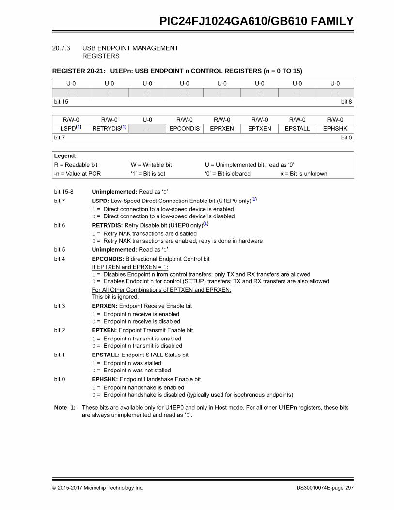
PIC24FJ1024GA610/GB610 FAMILY
20.7.3 USB ENDPOINT MANAGEMENT REGISTERS
REGISTER 20-21: U1EPn: USB ENDPOINT n CONTROL REGISTERS (n = 0 TO 15)
U-0 U-0 U-0 U-0 U-0 U-0 U-0 U-0
— — — — — — — —
bit 15 bit 8
R/W-0 R/W-0 U-0 R/W-0 R/W-0 R/W-0 R/W-0 R/W-0
LSPD(1) RETRYDIS(1) — EPCONDIS EPRXEN EPTXEN EPSTALL EPHSHK
bit 7 bit 0
Legend:
R = Readable bit W = Writable bit U = Unimplemented bit, read as ‘0’
-n = Value at POR ‘1’ = Bit is set ‘0’ = Bit is cleared x = Bit is unknown
bit 15-8 Unimplemented: Read as ‘0’
bit 7 LSPD: Low-Speed Direct Connection Enable bit (U1EP0 only)(1)
1 = Direct connection to a low-speed device is enabled0 = Direct connection to a low-speed device is disabled
bit 6 RETRYDIS: Retry Disable bit (U1EP0 only)(1)
1 = Retry NAK transactions are disabled0 = Retry NAK transactions are enabled; retry is done in hardware
bit 5 Unimplemented: Read as ‘0’
bit 4 EPCONDIS: Bidirectional Endpoint Control bit
If EPTXEN and EPRXEN = 1:1 = Disables Endpoint n from control transfers; only TX and RX transfers are allowed0 = Enables Endpoint n for control (SETUP) transfers; TX and RX transfers are also allowed
For All Other Combinations of EPTXEN and EPRXEN:This bit is ignored.
bit 3 EPRXEN: Endpoint Receive Enable bit
1 = Endpoint n receive is enabled0 = Endpoint n receive is disabled
bit 2 EPTXEN: Endpoint Transmit Enable bit
1 = Endpoint n transmit is enabled0 = Endpoint n transmit is disabled
bit 1 EPSTALL: Endpoint STALL Status bit
1 = Endpoint n was stalled0 = Endpoint n was not stalled
bit 0 EPHSHK: Endpoint Handshake Enable bit
1 = Endpoint handshake is enabled0 = Endpoint handshake is disabled (typically used for isochronous endpoints)
Note 1: These bits are available only for U1EP0 and only in Host mode. For all other U1EPn registers, these bits are always unimplemented and read as ‘0’.
2015-2017 Microchip Technology Inc. DS30010074E-page 297

PIC24FJ1024GA610/GB610 FAMILY
NOTES:
DS30010074E-page 298 2015-2017 Microchip Technology Inc.

PIC24FJ1024GA610/GB610 FAMILY
21.0 ENHANCED PARALLEL MASTER PORT (EPMP)
The Enhanced Parallel Master Port (EPMP) module pro-vides a parallel, 4-bit (Master mode only), 8-bit (Masterand Slave modes) or 16-bit (Master mode only) data businterface to communicate with off-chip modules, such asmemories, FIFOs, LCD controllers and other micro-controllers. This module can serve as either the masteror the slave on the communication bus.
For EPMP Master modes, all external addresses aremapped into the internal Extended Data Space (EDS).This is done by allocating a region of the EDS for eachChip Select, and then assigning each Chip Select to aparticular external resource, such as a memory orexternal controller. This region should not be assignedto another device resource, such as RAM or SFRs. Toperform a write or read on an external resource, theCPU simply performs a write or read within the addressrange assigned for the EPMP.
Key features of the EPMP module are:
• Extended Data Space (EDS) Interface Allows Direct Access from the CPU
• Up to 23 Programmable Address Lines
• Up to 2 Chip Select lines
• Up to 2 Acknowledgment Lines (one per Chip Select)
• 4-Bit, 8-Bit or 16-Bit Wide Data Bus
• Programmable Strobe Options (per Chip Select):
- Individual read and write strobes or;
- Read/Write strobe with enable strobe
• Programmable Address/Data Multiplexing
• Programmable Address Wait States
• Programmable Data Wait States (per Chip Select)
• Programmable Polarity on Control Signals (per Chip Select)
• Legacy Parallel Slave Port Support
• Enhanced Parallel Slave Support:
- Address support
- 4-byte deep auto-incrementing buffer
21.1 Specific Package Variations
While all PIC24FJ1024GA610/GB610 family devicesimplement the EPMP, I/O pin constraints place somelimits on 16-Bit Master mode operations in some pack-age types. This is reflected in the number of dedicatedChip Select pins implemented and the number of dedi-cated address lines that are available. The differencesare summarized in Table 21-1. All available EPMP pinfunctions are summarized in Table 21-2.
For 64-pin devices, the dedicated Chip Select pins(PMCS1 and PMCS2) are not implemented. In addi-tion, only 16 address lines (PMA<15:0>) are available.If required, PMA14 and PMA15 can be remapped tofunction as PMCS1 and PMCS2, respectively.
The memory space addressable by the devicedepends on the number of address lines available, aswell as the number of Chip Select signals required forthe application. Devices with lower pin counts are moreaffected by Chip Select requirements, as these takeaway address lines. Table 21-1 shows the maximumaddressable range for each pin count.
21.2 PMDOUT1 and PMDOUT2 Registers
The EPMP Data Output 1 and Data Output 2 registersare used only in Slave mode for buffered output data.These registers act as a buffer for outgoing data.
21.3 PMDIN1 and PMDIN2 Registers
The EPMP Data Input 1 and Data Input 2 registers areused in Slave modes to buffer incoming data. Theseregisters hold data that is asynchronously clocked in.
In Master mode, PMDIN1 is the holding register forincoming data.
TABLE 21-1: EPMP FEATURE DIFFERENCES BY DEVICE PIN COUNT
Note: This data sheet summarizes the features ofthis group of PIC24F devices. It is notintended to be a comprehensive referencesource. For more information, refer tothe “dsPIC33/PIC24 Family ReferenceManual”, “Enhanced Parallel MasterPort (EPMP)” (DS39730), which isavailable from the Microchip web site(www.microchip.com). The information inthis data sheet supersedes the informationin the FRM.
Device
Dedicated Chip Select Address
LinesDataLines
Address Range (bytes)
CS1 CS2 No CS 1 CS(1) 2 CS(1)
PIC24FJXXXGX606 (64-Pin) — — 16 8 64K 32K 16K
PIC24FJXXXGX610 (100-Pin/121-Pin) X X 23 16 16M
Note 1: PMA14 and PMA15 can be remapped to be dedicated Chip Selects.
2015-2017 Microchip Technology Inc. DS30010074E-page 299

PIC24FJ1024GA610/GB610 FAMILY
TABLE 21-2: ENHANCED PARALLEL MASTER PORT PIN DESCRIPTIONS
Pin Name(Alternate Function)
Type Description
PMA<22:16> O Address Bus bits<22:16>
PMA15 O Address Bus bit 15
I/O Data Bus bit 15 (16-bit port with Multiplexed Addressing)
(PMCS2) O Chip Select 2 (alternate location)
PMA14 O Address Bus bit 14
I/O Data Bus bit 14 (16-bit port with Multiplexed Addressing)
(PMCS1) O Chip Select 1 (alternate location)
PMA<13:8> O Address Bus bits<13:8>
I/O Data Bus bits<13:8> (16-bit port with Multiplexed Addressing)
PMA<7:3> O Address Bus bits<7:3>
PMA2 (PMALU)
O Address Bus bit 2
O Address Latch Upper Strobe for Multiplexed Address
PMA1(PMALH)
I/O Address Bus bit 1
O Address Latch High Strobe for Multiplexed Address
PMA0(PMALL)
I/O Address Bus bit 0
O Address Latch Low Strobe for Multiplexed Address
PMD<15:8> I/O Data Bus bits<15:8> (Demultiplexed Addressing)
PMD<7:4> I/O Data Bus bits<7:4>
O Address Bus bits<7:4> (4-bit port with 1-Phase Multiplexed Addressing)
PMD<3:0> I/O Data Bus bits<3:0>
PMCS1(1) O Chip Select 1
PMCS2(1) O Chip Select 2
PMWR I/O Write Strobe(2)
(PMENB) I/O Enable Signal(2)
PMRD I/O Read Strobe(2)
(PMRD/PMWR) I/O Read/Write Signal(2)
PMBE1 O Byte Indicator
PMBE0 O Nibble or Byte Indicator
PMACK1 I Acknowledgment Signal 1
PMACK2 I Acknowledgment Signal 2
Note 1: These pins are implemented in 100-pin and 121-pin devices only.
2: Signal function depends on the setting of the MODE<1:0> and SM bits (PMCON1<9:8> and PMCSxCF<8>).
DS30010074E-page 300 2015-2017 Microchip Technology Inc.

PIC24FJ1024GA610/GB610 FAMILY
REGISTER 21-1: PMCON1: EPMP CONTROL REGISTER 1
R/W-0 U-0 R/W-0 R/W-0 R/W-0 U-0 R/W-0 R/W-0
PMPEN — PSIDL ADRMUX1 ADRMUX0 — MODE1 MODE0
bit 15 bit 8
R/W-0 R/W-0 R/W-0 R/W-0 U-0 R/W-0 R/W-0 R/W-0
CSF1 CSF0 ALP ALMODE — BUSKEEP IRQM1 IRQM0
bit 7 bit 0
Legend:
R = Readable bit W = Writable bit U = Unimplemented bit, read as ‘0’
-n = Value at POR ‘1’ = Bit is set ‘0’ = Bit is cleared x = Bit is unknown
bit 15 PMPEN: Parallel Master Port Enable bit
1 = EPMP is enabled0 = EPMP is disabled
bit 14 Unimplemented: Read as ‘0’
bit 13 PSIDL: Parallel Master Port Stop in Idle Mode bit
1 = Discontinues module operation when device enters Idle mode0 = Continues module operation in Idle mode
bit 12-11 ADRMUX<1:0>: Address/Data Multiplexing Selection bits
11 = Lower address bits are multiplexed with data bits using 3 address phases10 = Lower address bits are multiplexed with data bits using 2 address phases01 = Lower address bits are multiplexed with data bits using 1 address phase00 = Address and data appear on separate pins
bit 10 Unimplemented: Read as ‘0’
bit 9-8 MODE<1:0>: Parallel Port Mode Select bits
11 = Master mode10 = Enhanced PSP; pins used are PMRD, PMWR, PMCS, PMD<7:0> and PMA<1:0>01 = Buffered PSP; pins used are PMRD, PMWR, PMCS and PMD<7:0>00 = Legacy Parallel Slave Port; pins used are PMRD, PMWR, PMCS and PMD<7:0>
bit 7-6 CSF<1:0>: Chip Select Function bits
11 = Reserved10 = PMA15 is used for Chip Select 2, PMA14 is used for Chip Select 101 = PMA15 is used for Chip Select 2, PMCS1 is used for Chip Select 100 = PMCS2 is used for Chip Select 2, PMCS1 is used for Chip Select 1
bit 5 ALP: Address Latch Polarity bit
1 = Active-high (PMALL, PMALH and PMALU)0 = Active-low (PMALL, PMALH and PMALU)
bit 4 ALMODE: Address Latch Strobe Mode bit
1 = Enables “smart” address strobes (each address phase is only present if the current access wouldcause a different address in the latch than the previous address)
0 = Disables “smart” address strobes
bit 3 Unimplemented: Read as ‘0’
bit 2 BUSKEEP: Bus Keeper bit
1 = Data bus keeps its last value when not actively being driven0 = Data bus is in a high-impedance state when not actively being driven
bit 1-0 IRQM<1:0>: Interrupt Request Mode bits
11 = Interrupt is generated when Read Buffer 3 is read or Write Buffer 3 is written (Buffered PSP mode),or on a read or write operation when PMA<1:0> = 11 (Addressable PSP mode only)
10 = Reserved01 = Interrupt is generated at the end of a read/write cycle00 = No interrupt is generated
2015-2017 Microchip Technology Inc. DS30010074E-page 301
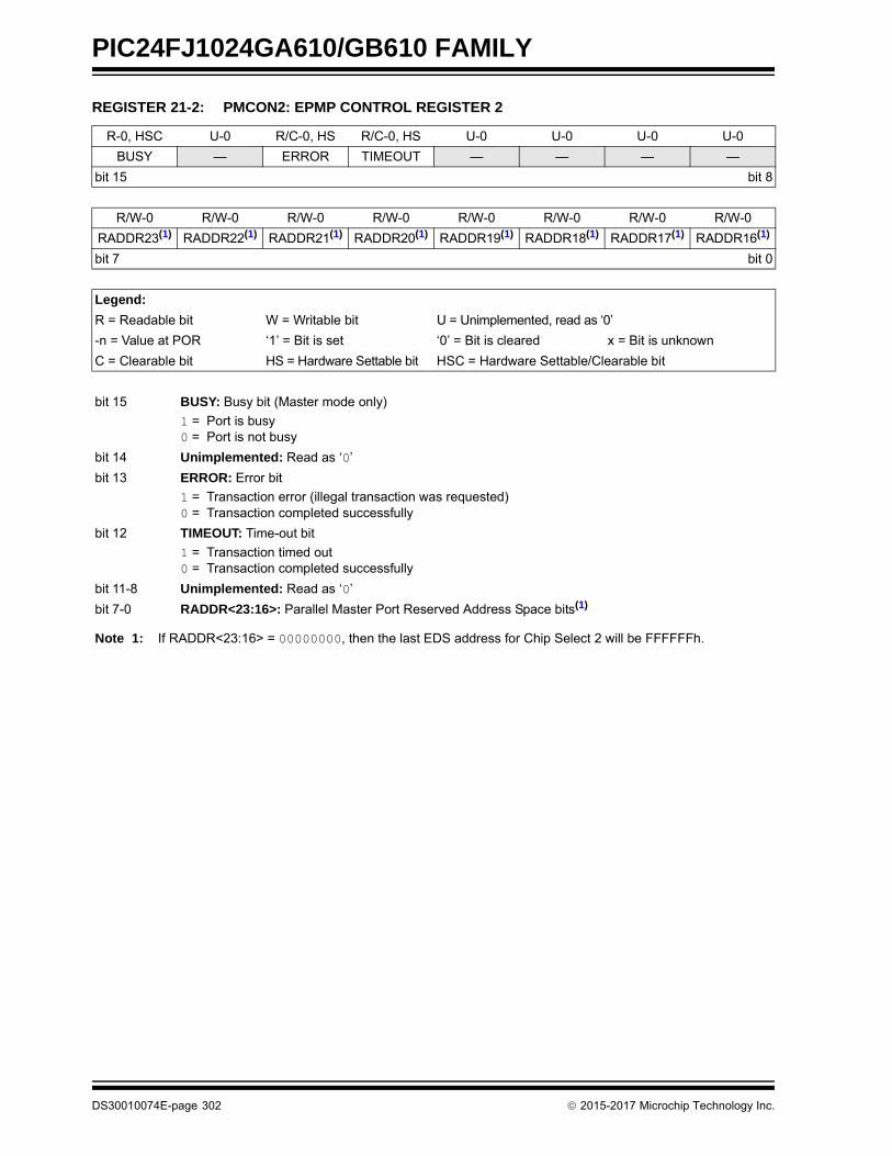
PIC24FJ1024GA610/GB610 FAMILY
REGISTER 21-2: PMCON2: EPMP CONTROL REGISTER 2
R-0, HSC U-0 R/C-0, HS R/C-0, HS U-0 U-0 U-0 U-0
BUSY — ERROR TIMEOUT — — — —
bit 15 bit 8
R/W-0 R/W-0 R/W-0 R/W-0 R/W-0 R/W-0 R/W-0 R/W-0
RADDR23(1) RADDR22(1) RADDR21(1) RADDR20(1) RADDR19(1) RADDR18(1) RADDR17(1) RADDR16(1)
bit 7 bit 0
Legend:
R = Readable bit W = Writable bit U = Unimplemented, read as ‘0’
-n = Value at POR ‘1’ = Bit is set ‘0’ = Bit is cleared x = Bit is unknown
C = Clearable bit HS = Hardware Settable bit HSC = Hardware Settable/Clearable bit
bit 15 BUSY: Busy bit (Master mode only)
1 = Port is busy0 = Port is not busy
bit 14 Unimplemented: Read as ‘0’
bit 13 ERROR: Error bit
1 = Transaction error (illegal transaction was requested)0 = Transaction completed successfully
bit 12 TIMEOUT: Time-out bit
1 = Transaction timed out0 = Transaction completed successfully
bit 11-8 Unimplemented: Read as ‘0’
bit 7-0 RADDR<23:16>: Parallel Master Port Reserved Address Space bits(1)
Note 1: If RADDR<23:16> = 00000000, then the last EDS address for Chip Select 2 will be FFFFFFh.
DS30010074E-page 302 2015-2017 Microchip Technology Inc.
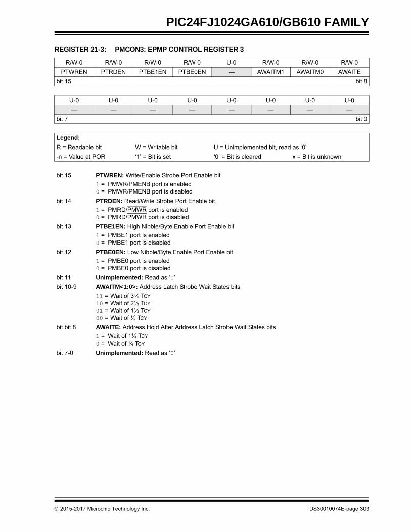
PIC24FJ1024GA610/GB610 FAMILY
REGISTER 21-3: PMCON3: EPMP CONTROL REGISTER 3
R/W-0 R/W-0 R/W-0 R/W-0 U-0 R/W-0 R/W-0 R/W-0
PTWREN PTRDEN PTBE1EN PTBE0EN — AWAITM1 AWAITM0 AWAITE
bit 15 bit 8
U-0 U-0 U-0 U-0 U-0 U-0 U-0 U-0
— — — — — — — —
bit 7 bit 0
Legend:
R = Readable bit W = Writable bit U = Unimplemented bit, read as ‘0’
-n = Value at POR ‘1’ = Bit is set ‘0’ = Bit is cleared x = Bit is unknown
bit 15 PTWREN: Write/Enable Strobe Port Enable bit
1 = PMWR/PMENB port is enabled0 = PMWR/PMENB port is disabled
bit 14 PTRDEN: Read/Write Strobe Port Enable bit
1 = PMRD/PMWR port is enabled0 = PMRD/PMWR port is disabled
bit 13 PTBE1EN: High Nibble/Byte Enable Port Enable bit
1 = PMBE1 port is enabled0 = PMBE1 port is disabled
bit 12 PTBE0EN: Low Nibble/Byte Enable Port Enable bit
1 = PMBE0 port is enabled0 = PMBE0 port is disabled
bit 11 Unimplemented: Read as ‘0’
bit 10-9 AWAITM<1:0>: Address Latch Strobe Wait States bits
11 = Wait of 3½ TCY
10 = Wait of 2½ TCY
01 = Wait of 1½ TCY
00 = Wait of ½ TCY
bit bit 8 AWAITE: Address Hold After Address Latch Strobe Wait States bits
1 = Wait of 1¼ TCY
0 = Wait of ¼ TCY
bit 7-0 Unimplemented: Read as ‘0’
2015-2017 Microchip Technology Inc. DS30010074E-page 303

PIC24FJ1024GA610/GB610 FAMILY
REGISTER 21-4: PMCON4: EPMP CONTROL REGISTER 4
R/W-0 R/W-0 R/W-0 R/W-0 R/W-0 R/W-0 R/W-0 R/W-0
PTEN15 PTEN14 PTEN<13:8>
bit 15 bit 8
R/W-0 R/W-0 R/W-0 R/W-0 R/W-0 R/W-0 R/W-0 R/W-0
PTEN<7:3> PTEN<2:0>
bit 7 bit 0
Legend:
R = Readable bit W = Writable bit U = Unimplemented bit, read as ‘0’
-n = Value at POR ‘1’ = Bit is set ‘0’ = Bit is cleared x = Bit is unknown
bit 15 PTEN15: PMA15 Port Enable bit
1 = PMA15 functions as either Address Line 15 or Chip Select 20 = PMA15 functions as port I/O
bit 14 PTEN14: PMA14 Port Enable bit
1 = PMA14 functions as either Address Line 14 or Chip Select 10 = PMA14 functions as port I/O
bit 13-3 PTEN<13:3>: EPMP Address Port Enable bits
1 = PMA<13:3> function as EPMP address lines0 = PMA<13:3> function as port I/Os
bit 2-0 PTEN<2:0>: PMALU/PMALH/PMALL Strobe Enable bits
1 = PMA<2:0> function as either address lines or address latch strobes0 = PMA<2:0> function as port I/Os
DS30010074E-page 304 2015-2017 Microchip Technology Inc.

PIC24FJ1024GA610/GB610 FAMILY
REGISTER 21-5: PMCSxCF: EPMP CHIP SELECT x CONFIGURATION REGISTER
R/W-0 R/W-0 R/W-0 R/W-0 U-0 R/W-0 R/W-0 R/W-0
CSDIS CSP CSPTEN BEP — WRSP RDSP SM
bit 15 bit 8
R/W-0 R/W-0 R/W-0 U-0 U-0 U-0 U-0 U-0
ACKP PTSZ1 PTSZ0 — — — — —
bit 7 bit 0
Legend:
R = Readable bit W = Writable bit U = Unimplemented bit, read as ‘0’
-n = Value at POR ‘1’ = Bit is set ‘0’ = Bit is cleared x = Bit is unknown
bit 15 CSDIS: Chip Select x Disable bit
1 = Disables the Chip Select x functionality0 = Enables the Chip Select x functionality
bit 14 CSP: Chip Select x Polarity bit
1 = Active-high (PMCSx)0 = Active-low (PMCSx)
bit 13 CSPTEN: PMCSx Port Enable bit
1 = PMCSx port is enabled0 = PMCSx port is disabled
bit 12 BEP: Chip Select x Nibble/Byte Enable Polarity bit
1 = Nibble/byte enable is active-high (PMBE0, PMBE1)0 = Nibble/byte enable is active-low (PMBE0, PMBE1)
bit 11 Unimplemented: Read as ‘0’
bit 10 WRSP: Chip Select x Write Strobe Polarity bit
For Slave modes and Master mode when SM = 0:1 = Write strobe is active-high (PMWR)0 = Write strobe is active-low (PMWR)
For Master mode when SM = 1:1 = Enable strobe is active-high (PMENB)0 = Enable strobe is active-low (PMENB)
bit 9 RDSP: Chip Select x Read Strobe Polarity bit
For Slave modes and Master mode when SM = 0:1 = Read strobe is active-high (PMRD)0 = Read strobe is active-low (PMRD)
For Master mode when SM = 1:1 = Read/write strobe is active-high (PMRD/PMWR)0 = Read/Write strobe is active-low (PMRD/PMWR)
bit 8 SM: Chip Select x Strobe Mode bit
1 = Reads/writes and enables strobes (PMRD/PMWR and PMENB)0 = Reads and writes strobes (PMRD and PMWR)
bit 7 ACKP: Chip Select x Acknowledge Polarity bit
1 = ACK is active-high (PMACK1)0 = ACK is active-low (PMACK1)
bit 6-5 PTSZ<1:0>: Chip Select x Port Size bits
11 = Reserved10 = 16-bit port size (PMD<15:0>)01 = 4-bit port size (PMD<3:0>)00 = 8-bit port size (PMD<7:0>)
bit 4-0 Unimplemented: Read as ‘0’
2015-2017 Microchip Technology Inc. DS30010074E-page 305

PIC24FJ1024GA610/GB610 FAMILY
REGISTER 21-6: PMCSxBS: EPMP CHIP SELECT x BASE ADDRESS REGISTER(2)
R/W(1) R/W(1) R/W(1) R/W(1) R/W(1) R/W(1) R/W(1) R/W(1)
BASE<23:16>
bit 15 bit 8
R/W(1) U-0 U-0 U-0 R/W(1) U-0 U-0 U-0
BASE15 — — — BASE11 — — —
bit 7 bit 0
Legend:
R = Readable bit W = Writable bit U = Unimplemented bit, read as ‘0’
-n = Value at POR ‘1’ = Bit is set ‘0’ = Bit is cleared x = Bit is unknown
bit 15-7 BASE<23:15>: Chip Select x Base Address bits(1)
bit 6-4 Unimplemented: Read as ‘0’
bit 3 BASE11: Chip Select x Base Address bit(1)
bit 2-0 Unimplemented: Read as ‘0’
Note 1: The value at POR is 0080h for PMCS1BS and 8080h for PMCS2BS.
2: If the whole PMCS2BS register is written together as 0x0000, then the last EDS address for the Chip Select 1 will be FFFFFFh. In this case, Chip Select 2 should not be used. PMCS1BS has no such feature.
DS30010074E-page 306 2015-2017 Microchip Technology Inc.

PIC24FJ1024GA610/GB610 FAMILY
REGISTER 21-7: PMCSxMD: EPMP CHIP SELECT x MODE REGISTER
R/W-0 R/W-0 R/W-0 R/W-0 R/W-0 U-0 U-0 U-0
ACKM1 ACKM0 AMWAIT2 AMWAIT1 AMWAIT0 — — —
bit 15 bit 8
R/W-0 R/W-0 R/W-0 R/W-0 R/W-0 R/W-0 R/W-0 R/W-0
DWAITB1 DWAITB0 DWAITM3 DWAITM2 DWAITM1 DWAITM0 DWAITE1 DWAITE0
bit 7 bit 0
Legend:
R = Readable bit W = Writable bit U = Unimplemented bit, read as ‘0’
-n = Value at POR ‘1’ = Bit is set ‘0’ = Bit is cleared x = Bit is unknown
bit 15-14 ACKM<1:0>: Chip Select x Acknowledge Mode bits
11 = Reserved10 = PMACKx is used to determine when a read/write operation is complete01 = PMACKx is used to determine when a read/write operation is complete with time-out
(If DWAITM<3:0> = 0000, the maximum time-out is 255 TCY or else it is DWAITM<3:0> cycles.)00 = PMACKx is not used
bit 13-11 AMWAIT<2:0>: Chip Select x Alternate Master Wait States bits
111 = Wait of 10 alternate master cycles. . .001 = Wait of 4 alternate master cycles000 = Wait of 3 alternate master cycles
bit 10-8 Unimplemented: Read as ‘0’
bit 7-6 DWAITB<1:0>: Chip Select x Data Setup Before Read/Write Strobe Wait States bits
11 = Wait of 3¼ TCY
10 = Wait of 2¼ TCY
01 = Wait of 1¼ TCY
00 = Wait of ¼ TCY
bit 5-2 DWAITM<3:0>: Chip Select x Data Read/Write Strobe Wait States bits
For Write Operations:1111 = Wait of 15½ TCY
. . .0001 = Wait of 1½ TCY
0000 = Wait of ½ TCY
For Read Operations:1111 = Wait of 15¾ TCY
. . .0001 = Wait of 1¾ TCY
0000 = Wait of ¾ TCY
bit 1-0 DWAITE<1:0>: Chip Select x Data Hold After Read/Write Strobe Wait States bits
For Write Operations:11 = Wait of 3¼ TCY
10 = Wait of 2¼ TCY
01 = Wait of 1¼ TCY
00 = Wait of ¼ TCY
For Read Operations:11 = Wait of 3 TCY
10 = Wait of 2 TCY
01 = Wait of 1 TCY
00 = Wait of 0 TCY
2015-2017 Microchip Technology Inc. DS30010074E-page 307

PIC24FJ1024GA610/GB610 FAMILY
REGISTER 21-8: PMSTAT: EPMP STATUS REGISTER (SLAVE MODE ONLY)
R-0, HSC R/W-0, HS U-0 U-0 R-0, HSC R-0, HSC R-0, HSC R-0, HSC
IBF IBOV — — IB3F(1) IB2F(1) IB1F(1) IB0F(1)
bit 15 bit 8
R-1, HSC R/W-0, HS U-0 U-0 R-1, HSC R-1, HSC R-1, HSC R-1, HSC
OBE OBUF — — OB3E OB2E OB1E OB0E
bit 7 bit 0
Legend: HS = Hardware Settable bit HSC = Hardware Settable/Clearable bit
R = Readable bit W = Writable bit U = Unimplemented bit, read as ‘0’
-n = Value at POR ‘1’ = Bit is set ‘0’ = Bit is cleared x = Bit is unknown
bit 15 IBF: Input Buffer Full Status bit
1 = All writable Input Buffer registers are full0 = Some or all of the writable Input Buffer registers are empty
bit 14 IBOV: Input Buffer Overflow Status bit
1 = A write attempt to a full Input register occurred (must be cleared in software)0 = No overflow occurred
bit 13-12 Unimplemented: Read as ‘0’
bit 11-8 IB3F:IB0F: Input Buffer x Status Full bits(1)
1 = Input buffer contains unread data (reading the buffer will clear this bit)0 = Input buffer does not contain unread data
bit 7 OBE: Output Buffer Empty Status bit
1 = All readable Output Buffer registers are empty0 = Some or all of the readable Output Buffer registers are full
bit 6 OBUF: Output Buffer Underflow Status bit
1 = A read occurred from an empty Output Buffer register (must be cleared in software)0 = No underflow occurred
bit 5-4 Unimplemented: Read as ‘0’
bit 3-0 OB3E:OB0E: Output Buffer x Status Empty bit
1 = Output Buffer x is empty (writing data to the buffer will clear this bit)0 = Output Buffer x contains untransmitted data
Note 1: Even though an individual bit represents the byte in the buffer, the bits corresponding to the word (Byte 0 and 1, or Byte 2 and 3) get cleared, even on byte reading.
DS30010074E-page 308 2015-2017 Microchip Technology Inc.

PIC24FJ1024GA610/GB610 FAMILY
REGISTER 21-9: PADCON: PAD CONFIGURATION CONTROL REGISTER
R/W-0 U-0 U-0 U-0 U-0 U-0 U-0 U-0
IOCON — — — — — — —
bit 15 bit 8
U-0 U-0 U-0 U-0 U-0 U-0 U-0 R/W-0
— — — — — — — PMPTTL
bit 7 bit 0
Legend:
R = Readable bit W = Writable bit U = Unimplemented bit, read as ‘0’
-n = Value at POR ‘1’ = Bit is set ‘0’ = Bit is cleared x = Bit is unknown
bit 15 IOCON: Used for Non-PMP Functionality bit
bit 14-1 Unimplemented: Read as ‘0’
bit 0 PMPTTL: EPMP Module TTL Input Buffer Select bit
1 = EPMP module inputs (PMDx, PMCS1) use TTL input buffers0 = EPMP module inputs use Schmitt Trigger input buffers
2015-2017 Microchip Technology Inc. DS30010074E-page 309

PIC24FJ1024GA610/GB610 FAMILY
NOTES:
DS30010074E-page 310 2015-2017 Microchip Technology Inc.

PIC24FJ1024GA610/GB610 FAMILY
22.0 REAL-TIME CLOCK AND CALENDAR WITH TIMESTAMP
The RTCC provides the user with a Real-Time Clockand Calendar (RTCC) function that can be calibrated.
Key features of the RTCC module are:
• Selectable Clock Source
• Provides Hours, Minutes and Seconds Using 24-Hour Format
• Visibility of One Half Second Period
• Provides Calendar – Weekday, Date, Month and Year
• Alarm-Configurable for Half a Second, 1 Second, 10 Seconds, 1 Minute, 10 Minutes, 1 Hour, 1 Day, 1 Week, 1 Month or 1 Year
• Alarm Repeat with Decrementing Counter
• Alarm with Indefinite Repeat Chime
• Year 2000 to 2099 Leap Year Correction
• BCD Format for Smaller Software Overhead
• Optimized for Long-Term Battery Operation
• User Calibration of the 32.768 kHz Clock Crystal/32K INTRC Frequency with Periodic Auto-Adjust
• Fractional Second Synchronization
• Calibration to within ±2.64 Seconds Error per Month
• Calibrates up to 260 ppm of Crystal Error
• Ability to Periodically Wake-up External Devices without CPU Intervention (external power control)
• Power Control Output for External Circuit Control
• Calibration takes Effect Every 15 Seconds
• Timestamp Capture Register for Time and Date
• Programmable Prescaler and Clock Divider Circuit Allows Operation with Any Clock Source up to 32 MHz, Including 32.768 kHz Crystal, 50/60 Hz Powerline Clock, External Real-Time Clock (RTC) or 31.25 kHz LPRC Clock
22.1 RTCC Source Clock
The RTCC clock divider block converts the incomingoscillator source into accurate 1/2 and 1 second clocksfor the RTCC. The clock divider is optimized to workwith three different oscillator sources:
• 32.768 kHz Crystal Oscillator
• 31 kHz Low-Power RC Oscillator (LPRC)
• External 50 Hz or 60 Hz Powerline Frequency
An asynchronous prescaler, PS<1:0> (RTCCON2L<5:4>),is provided that allows the RTCC to work with higherspeed clock sources, such as the system clock. Divideratios of 1:16, 1:64 or 1:256 may be selected, allowingsources up to 32 MHz to clock the RTCC.
22.1.1 COARSE FREQUENCY DIVISION
The clock divider block has a 16-bit counter used todivide the input clock frequency. The divide ratio is setby the DIV<15:0> register bits (RTCCON2H<15:0>).The DIV<15:0> bits should be programmed with avalue to produce a nominal 1/2 second clock dividercount period.
22.1.2 FINE FREQUENCY DIVISION
The fine frequency division is set using the FDIV<4:0>(RTCCON2L<15:11>) bits. Increasing the FDIVx valuewill lengthen the overall clock divider period.
If FDIV<4:0> = 00000, the fine frequency division circuitis effectively disabled. Otherwise, it will optionallyremove a clock pulse from the input of the clock dividerevery 1/2 second. This functionality will allow the user toremove up to 31 pulses over a fixed period of16 seconds, depending on the value of FDIVx.
The value for DIV<15:0> is calculated as shown inEquation 22-1. The fractional remainder of theDIV<15:0> calculation result can be used to calculatethe value for FDIV<4:0>.
EQUATION 22-1: RTCC CLOCK DIVIDER OUTPUT FREQUENCY
Note: This data sheet summarizes the features ofthis group of PIC24F devices. It is notintended to be a comprehensive referencesource. For more information on theReal-Time Clock and Calendar, refer tothe “dsPIC33/PIC24 Family ReferenceManual”, “RTCC with Timestamp”(DS70005193), which is available from theMicrochip web site (www.microchip.com).The information in this data sheetsupersedes the information in the FRM.
The DIV<15:0> value is the integer part of this calculation:
The FDIV<4:0> value is the fractional part of the DIV<15:0>calculation multiplied by 32.
FOUT =FIN
2 • (PS<1:0> Prescaler) • (DIV<15:0> + 1) +FDIV<4:0>
32( )
DIV<15:0> =FIN
2 • (PS<1:0> Prescaler)– 1
2015-2017 Microchip Technology Inc. DS30010074E-page 311

PIC24FJ1024GA610/GB610 FAMILY
FIGURE 22-1: RTCC BLOCK DIAGRAM
RTCC
RTCOE
CLKSEL<1:0>
Alarm Registers
ComparatorsPowerControl
RepeatControl
Time/DateRegisters
Timestamp Time/Date Registers
PC<1:0>
PWCPS<1:0>
1/2Second
OUTSEL<2:0>
ClockDivider
PPS
DS30010074E-page 312 2015-2017 Microchip Technology Inc.

PIC24FJ1024GA610/GB610 FAMILY
22.2 RTCC Module Registers
The RTCC module registers are organized into fourcategories:
• RTCC Control Registers
• RTCC Value Registers
• Alarm Value Registers
• Timestamp Registers
22.2.1 REGISTER MAPPING
Previous RTCC implementations used a RegisterPointer to access the RTCC Time and Date registers,as well as the Alarm Time and Date registers. TheseRegisters are now mapped to memory and areindividually addressable.
22.2.2 WRITE LOCK
To prevent spurious changes to the RTCC Control orRTCC Value registers, the WRLOCK bit(RTCCON1L<11>) must be cleared (‘0’). The PORdefault state is the WRLOCK bit is ‘0’ and is cleared onany device Reset (POR, BOR, MCLR). It is recom-mended that the WRLOCK bit be set to ‘1’ after theRTCC Value registers are properly initialized, and afterthe RTCEN bit (RTCCON1L<15>) has been set.
Any attempt to write to the RTCEN bit, the RTCCON2L/Hregisters or the RTCC Value registers, will be ignoredas long as WRLOCK is ‘1’. The RTCC Control, AlarmValue and Timestamp registers can be changed whenWRLOCK is ‘1’.
Clearing the WRLOCK bit requires an unlock sequenceafter it has been written to a ‘1’, writing two bytesconsecutively to the NVMKEY register. A sampleassembly sequence is shown in Example 22-1. IfWRLOCK is already cleared, it can be set to ‘1’ withoutusing the unlock sequence.
22.2.3 SELECTING RTCC CLOCK SOURCE
The clock source for the RTCC module can be selectedusing the CLKSEL<1:0> bits in the RTCCON2Lregister. When the bits are set to ‘00’, the SecondaryOscillator (SOSC) is used as the reference clock andwhen the bits are ‘01’, LPRC is used as the referenceclock. When CLKSEL<1:0> = 10, the external power-line (50 Hz and 60 Hz) is used as the clock source.When CLKSEL<1:0> = 11, the system clock is used asthe clock source.
EXAMPLE 22-1: SETTING THE WRLOCK BIT
Note: To avoid accidental writes to the timer, it isrecommended that the WRLOCK bit(RTCCON1L<11>) is kept clear at anyother time. For the WRLOCK bit to be set,there is only one instruction cycle timewindow allowed between the 55h/AAsequence and the setting of WRLOCK;therefore, it is recommended that codefollow the procedure in Example 22-1.
DISI #6 ;disable interrupts for 6 instructionsMOV #NVKEY, W1MOV #0x55, W2 ; first unlock codeMOV W2, [W1] ; write first unlock codeMOV #0xAA, W3 ; second unlock sequenceMOV W3, [W1] ; write second unlock sequenceBCLR RTCCON1L, #WRLOCK ; clear the WRLOCK bit
2015-2017 Microchip Technology Inc. DS30010074E-page 313

PIC24FJ1024GA610/GB610 FAMILY
22.3 Registers
22.3.1 RTCC CONTROL REGISTERS
REGISTER 22-1: RTCCON1L: RTCC CONTROL REGISTER 1 (LOW)
R/W-0 U-0 U-0 U-0 R/W-0 R/W-0 R/W-0 R/W-0
RTCEN — — — WRLOCK PWCEN PWCPOL PWCPOE
bit 15 bit 8
R/W-0 R/W-0 R/W-0 R/W-0 U-0 U-0 U-0 R/W-0
RTCOE OUTSEL2 OUTSEL1 OUTSEL0 — — — TSAEN
bit 7 bit 0
Legend:
R = Readable bit W = Writable bit U = Unimplemented bit, read as ‘0’
-n = Value at POR ‘1’ = Bit is set ‘0’ = Bit is cleared x = Bit is unknown
bit 15 RTCEN: RTCC Enable bit
1 = RTCC is enabled and counts from selected clock source0 = RTCC is not enabled
bit 14-12 Unimplemented: Read as ‘0’
bit 11 WRLOCK: RTCC Register Write Lock
1 = RTCC registers are locked0 = RTCC registers may be written to by user
bit 10 PWCEN: Power Control Enable bit
1 = Power control is enabled0 = Power control is disabled
bit 9 PWCPOL: Power Control Polarity bit
1 = Power control output is active-high0 = Power control output is active-low
bit 8 PWCPOE: Power Control Output Enable bit
1 = Power control output pin is enabled0 = Power control output pin is disabled
bit 7 RTCOE: RTCC Output Enable bit
1 = RTCC output is enabled0 = RTCC output is disabled
bit 6-4 OUTSEL<2:0>: RTCC Output Signal Selection bits
111 = Unused110 = Unused101 = Unused100 = Timestamp A event011 = Power control010 = RTCC input clock001 = Second clock000 = Alarm event
bit 3-1 Unimplemented: Read as ‘0’
bit 0 TSAEN: Timestamp A Enable bit
1 = Timestamp event will occur when a low pulse is detected on the TMPR pin0 = Timestamp is disabled
DS30010074E-page 314 2015-2017 Microchip Technology Inc.

PIC24FJ1024GA610/GB610 FAMILY
REGISTER 22-2: RTCCON1H: RTCC CONTROL REGISTER 1 (HIGH)
R/W-0 R/W-0 U-0 U-0 R/W-0 R/W-0 R/W-0 R/W-0
ALRMEN CHIME — — AMASK3 AMASK2 AMASK1 AMASK0
bit 15 bit 8
R/W-0 R/W-0 R/W-0 R/W-0 R/W-0 R/W-0 R/W-0 R/W-0
ALMRPT7 ALMRPT6 ALMRPT5 ALMRPT4 ALMRPT3 ALMRPT2 ALMRPT1 ALMRPT0
bit 7 bit 0
Legend:
R = Readable bit W = Writable bit U = Unimplemented bit, read as ‘0’
-n = Value at POR ‘1’ = Bit is set ‘0’ = Bit is cleared x = Bit is unknown
bit 15 ALRMEN: Alarm Enable bit
1 = Alarm is enabled (cleared automatically after an alarm event whenever ALMRPT<7:0> = 00h andCHIME = 0)
0 = Alarm is disabled
bit 14 CHIME: Chime Enable bit
1 = Chime is enabled; ALMRPT<7:0> bits roll over from 00h to FFh0 = Chime is disabled; ALMRPT<7:0> bits stop once they reach 00h
bit 13-12 Unimplemented: Read as ‘0’
bit 11-8 AMASK<3:0>: Alarm Mask Configuration bits
0000 = Every half second0000 = Every second0010 = Every 10 seconds0011 = Every minute0100 = Every 10 minutes0101 = Every hour0110 = Once a day0111 = Once a week1000 = Once a month1001 = Once a year (except when configured for February 29th, once every 4 years)101x = Reserved – do not use11xx = Reserved – do not use
bit 7-0 ALMRPT<7:0>: Alarm Repeat Counter Value bits
11111111 = Alarm will repeat 255 more times•••00000000 = Alarm will repeat 0 more timesThe counter decrements on any alarm event. The counter is prevented from rolling over from ‘00’ to ‘FF’unless CHIME = 1.
2015-2017 Microchip Technology Inc. DS30010074E-page 315

PIC24FJ1024GA610/GB610 FAMILY
REGISTER 22-3: RTCCON2L: RTCC CONTROL REGISTER 2 (LOW)
R/W-0 R/W-0 R/W-0 R/W-0 R/W-0 U-0 U-0 U-0
FDIV4 FDIV3 FDIV2 FDIV1 FDIV0 — — —
bit 15 bit 8
R/W-0 R/W-0 R/W-0 R/W-0 U-0 U-0 R/W-0 R/W-0
PWCPS1 PWCPS0 PS1 PS0 — — CLKSEL1 CLKSEL0
bit 7 bit 0
Legend:
R = Readable bit W = Writable bit U = Unimplemented bit, read as ‘0’
-n = Value at POR ‘1’ = Bit is set ‘0’ = Bit is cleared x = Bit is unknown
bit 15-11 FDIV<4:0>: Fractional Clock Divide bits
00000 = No fractional clock division00001 = Increases period by 1 RTCC input clock cycle every 16 seconds00010 = Increases period by 2 RTCC input clock cycles every 16 seconds•••11101 = Increases period by 30 RTCC input clock cycles every 16 seconds11111 = Increases period by 31 RTCC input clock cycles every 16 seconds
bit 10-8 Unimplemented: Read as ‘0’
bit 7-6 PWCPS<1:0>: Power Control Prescale Select bits
00 = 1:101 = 1:1610 = 1:6411 = 1:256
bit 5-4 PS<1:0>: Prescale Select bits00 = 1:101 = 1:1610 = 1:6411 = 1:256
bit 3-2 Unimplemented: Read as ‘0’
bit 1-0 CLKSEL<1:0>: Clock Select bits
00 = SOSC01 = LPRC10 = PWRLCLK pin11 = System clock
DS30010074E-page 316 2015-2017 Microchip Technology Inc.

PIC24FJ1024GA610/GB610 FAMILY
22.3.2 RTCVAL REGISTER MAPPINGS
REGISTER 22-4: RTCCON2H: RTCC CONTROL REGISTER 2 (HIGH)(1)
R/W-0 R/W-0 R/W-1 R/W-1 R/W-1 R/W-1 R/W-1 R/W-1
DIV<15:8>
bit 15 bit 8
R/W-1 R/W-1 R/W-1 R/W-1 R/W-1 R/W-1 R/W-1 R/W-1
DIV<7:0>
bit 7 bit 0
Legend:
R = Readable bit W = Writable bit U = Unimplemented bit, read as ‘0’
-n = Value at POR ‘1’ = Bit is set ‘0’ = Bit is cleared x = Bit is unknown
bit 15-0 DIV<15:0>: Clock Divide bits
Sets the period of the clock divider counter; value should cause a nominal 1/2 second underflow.
Note 1: A write to this register is only allowed when WRLOCK = 1.
2015-2017 Microchip Technology Inc. DS30010074E-page 317

PIC24FJ1024GA610/GB610 FAMILY
REGISTER 22-5: RTCCON3L: RTCC CONTROL REGISTER 3 (LOW)
R/W-0 R/W-0 R/W-0 R/W-0 R/W-0 R/W-0 R/W-0 R/W-0
PWCSAMP7 PWCSAMP6 PWCSAMP5 PWCSAMP4 PWCSAMP3 PWCSAMP2 PWCSAMP1 PWCSAMP0
bit 15 bit 8
R/W-0 R/W-0 R/W-0 R/W-0 R/W-0 R/W-0 R/W-0 R/W-0
PWCSTAB7 PWCSTAB6 PWCSTAB5 PWCSTAB4 PWCSTAB3 PWCSTAB2 PWCSTAB1 PWCSTAB0
bit 7 bit 0
Legend:
R = Readable bit W = Writable bit U = Unimplemented bit, read as ‘0’
-n = Value at POR ‘1’ = Bit is set ‘0’ = Bit is cleared x = Bit is unknown
bit 15-8 PWCSAMP<7:0>: Power Control Sample Window Timer bits
11111111 = Sample window is always enabled, even when PWCEN = 011111110 = Sample window is 254 TPWCCLK clock periods•••00000001 = Sample window is 1 TPWCCLK clock period00000000 = No sample window
bit 7-0 PWCSTAB<7:0>: Power Control Stability Window Timer bits(1)
11111111 = Stability window is 255 TPWCCLK clock periods11111110 = Stability window is 254 TPWCCLK clock periods•••00000001 = Stability window is 1 TPWCCLK clock period00000000 = No stability window; sample window starts when the alarm event triggers
Note 1: The sample window always starts when the stability window timer expires, except when its initial value is 00h.
DS30010074E-page 318 2015-2017 Microchip Technology Inc.
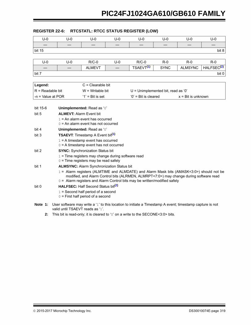
PIC24FJ1024GA610/GB610 FAMILY
REGISTER 22-6: RTCSTATL: RTCC STATUS REGISTER (LOW)
U-0 U-0 U-0 U-0 U-0 U-0 U-0 U-0
— — — — — — — —
bit 15 bit 8
U-0 U-0 R/C-0 U-0 R/C-0 R-0 R-0 R-0
— — ALMEVT — TSAEVT(1) SYNC ALMSYNC HALFSEC(2)
bit 7 bit 0
Legend: C = Clearable bit
R = Readable bit W = Writable bit U = Unimplemented bit, read as ‘0’
-n = Value at POR ‘1’ = Bit is set ‘0’ = Bit is cleared x = Bit is unknown
bit 15-6 Unimplemented: Read as ‘0’
bit 5 ALMEVT: Alarm Event bit
1 = An alarm event has occurred0 = An alarm event has not occurred
bit 4 Unimplemented: Read as ‘0’
bit 3 TSAEVT: Timestamp A Event bit(1)
1 = A timestamp event has occurred0 = A timestamp event has not occurred
bit 2 SYNC: Synchronization Status bit
1 = Time registers may change during software read0 = Time registers may be read safely
bit 1 ALMSYNC: Alarm Synchronization Status bit
1 = Alarm registers (ALMTIME and ALMDATE) and Alarm Mask bits (AMASK<3:0>) should not bemodified, and Alarm Control bits (ALRMEN, ALMRPT<7:0>) may change during software read
0 = Alarm registers and Alarm Control bits may be written/modified safely
bit 0 HALFSEC: Half Second Status bit(2)
1 = Second half period of a second0 = First half period of a second
Note 1: User software may write a ‘1’ to this location to initiate a Timestamp A event; timestamp capture is not valid until TSAEVT reads as ‘1’.
2: This bit is read-only; it is cleared to ‘0’ on a write to the SECONE<3:0> bits.
2015-2017 Microchip Technology Inc. DS30010074E-page 319

PIC24FJ1024GA610/GB610 FAMILY
22.3.3 RTCC VALUE REGISTERS
REGISTER 22-7: TIMEL: RTCC TIME REGISTER (LOW)
U-0 R/W-x R/W-x R/W-x R/W-x R/W-x R/W-x R/W-x
— SECTEN2 SECTEN1 SECTEN0 SECONE3 SECONE2 SECONE1 SECONE0
bit 15 bit 8
U-0 U-0 U-0 U-0 U-0 U-0 U-0 U-0
— — — — — — — —
bit 7 bit 0
Legend:
R = Readable bit W = Writable bit U = Unimplemented bit, read as ‘0’
-n = Value at POR ‘1’ = Bit is set ‘0’ = Bit is cleared x = Bit is unknown
bit 15 Unimplemented: Read as ‘0’
bit 14-12 SECTEN<2:0>: Binary Coded Decimal Value of Seconds ‘10’ Digit bits
Contains a value from 0 to 5.
bit 11-8 SECONE<3:0>: Binary Coded Decimal Value of Seconds ‘1’ Digit bits
Contains a value from 0 to 9.
bit 7-0 Unimplemented: Read as ‘0’
REGISTER 22-8: TIMEH: RTCC TIME REGISTER (HIGH)
U-0 U-0 R/W-0 R/W-x R/W-x R/W-x R/W-x R/W-x
— — HRTEN1 HRTEN0 HRONE3 HRONE2 HRONE1 HRONE0
bit 15 bit 8
U-0 R/W-0 R/W-0 R/W-x R/W-x R/W-x R/W-x R/W-x
— MINTEN2 MINTEN1 MINTEN0 MINONE3 MINONE2 MINONE1 MINONE0
bit 7 bit 0
Legend:
R = Readable bit W = Writable bit U = Unimplemented bit, read as ‘0’
-n = Value at POR ‘1’ = Bit is set ‘0’ = Bit is cleared x = Bit is unknown
bit 15-14 Unimplemented: Read as ‘0’
bit 13-12 HRTEN<1:0>: Binary Coded Decimal Value of Hours ‘10’ Digit bits
Contains a value from 0 to 2.
bit 11-8 HRONE<3:0>: Binary Coded Decimal Value of Hours ‘1’ Digit bits
Contains a value from 0 to 9.
bit 7 Unimplemented: Read as ‘0’
bit 6-4 MINTEN<2:0>: Binary Coded Decimal Value of Minutes ‘10’ Digit bits
Contains a value from 0 to 5.
bit 3-0 MINONE<3:0>: Binary Coded Decimal Value of Minutes ‘1’ Digit bits
Contains a value from 0 to 9.
DS30010074E-page 320 2015-2017 Microchip Technology Inc.

PIC24FJ1024GA610/GB610 FAMILY
REGISTER 22-9: DATEL: RTCC DATE REGISTER (LOW)
U-0 U-0 R/W-0 R/W-0 R/W-0 R/W-0 R/W-0 R/W-0
— — DAYTEN1 DAYTEN0 DAYONE3 DAYONE2 DAYONE1 DAYONE0
bit 15 bit 8
U-0 U-0 U-0 U-0 U-0 R/W-x R/W-x R/W-x
— — — — — WDAY2 WDAY1 WDAY0
bit 7 bit 0
Legend:
R = Readable bit W = Writable bit U = Unimplemented bit, read as ‘0’
-n = Value at POR ‘1’ = Bit is set ‘0’ = Bit is cleared x = Bit is unknown
bit 15-14 Unimplemented: Read as ‘0’
bit 13-12 DAYTEN<1:0>: Binary Coded Decimal Value of Days ‘10’ Digit bits
Contains a value from 0 to 3.
bit 11-8 DAYONE<3:0>: Binary Coded Decimal Value of Days ‘1’ Digit bits
Contains a value from 0 to 9.
bit 7-3 Unimplemented: Read as ‘0’
bit 2-0 WDAY<2:0>: Binary Coded Decimal Value of Weekdays ‘1’ Digit bits
Contains a value from 0 to 6.
REGISTER 22-10: DATEH: RTCC DATE REGISTER (HIGH)
R/W-0 R/W-0 R/W-0 R/W-0 R/W-x R/W-x R/W-x R/W-x
YRTEN3 YRTEN2 YRTEN1 YRTEN0 YRONE3 YRONE2 YRONE1 YRONE0
bit 15 bit 8
U-0 U-0 U-0 R/W-x R/W-x R/W-x R/W-x R/W-x
— — — MTHTEN MTHONE3 MTHONE2 MTHONE1 MTHONE0
bit 7 bit 0
Legend:
R = Readable bit W = Writable bit U = Unimplemented bit, read as ‘0’
-n = Value at POR ‘1’ = Bit is set ‘0’ = Bit is cleared x = Bit is unknown
bit 15-12 YRTEN<3:0>: Binary Coded Decimal Value of Years ‘10’ Digit bits
bit 11-8 YRONE<3:0>: Binary Coded Decimal Value of Years ‘1’ Digit bits
bit 7-5 Unimplemented: Read as ‘0’
bit 4 MTHTEN: Binary Coded Decimal Value of Months ‘10’ Digit bit
Contains a value from 0 to 1.
bit 3-0 MTHONE<3:0>: Binary Coded Decimal Value of Months ‘1’ Digit bits
Contains a value from 0 to 9.
2015-2017 Microchip Technology Inc. DS30010074E-page 321

PIC24FJ1024GA610/GB610 FAMILY
22.3.4 ALARM VALUE REGISTERS
REGISTER 22-11: ALMTIMEL: RTCC ALARM TIME REGISTER (LOW)
U-0 R/W-0 R/W-0 R/W-0 R/W-0 R/W-0 R/W-0 R/W-0
— SECTEN2 SECTEN1 SECTEN0 SECONE3 SECONE2 SECONE1 SECONE0
bit 15 bit 8
U-0 U-0 U-0 U-0 U-0 U-0 U-0 U-0
— — — — — — — —
bit 7 bit 0
Legend:
R = Readable bit W = Writable bit U = Unimplemented bit, read as ‘0’
-n = Value at POR ‘1’ = Bit is set ‘0’ = Bit is cleared x = Bit is unknown
bit 15 Unimplemented: Read as ‘0’
bit 14-12 SECTEN<2:0>: Binary Coded Decimal Value of Seconds ‘10’ Digit bits
Contains a value from 0 to 5.
bit 11-8 SECONE<3:0>: Binary Coded Decimal Value of Seconds ‘1’ Digit bits
Contains a value from 0 to 9.
bit 7-0 Unimplemented: Read as ‘0’
REGISTER 22-12: ALMTIMEH: RTCC ALARM TIME REGISTER (HIGH)
U-0 U-0 R/W-0 R/W-0 R/W-0 R/W-0 R/W-0 R/W-0
— — HRTEN1 HRTEN0 HRONE3 HRONE2 HRONE1 HRONE0
bit 15 bit 8
U-0 R/W-0 R/W-0 R/W-0 R/W-0 R/W-0 R/W-0 R/W-0
— MINTEN2 MINTEN1 MINTEN0 MINONE3 MINONE2 MINONE1 MINONE0
bit 7 bit 0
Legend:
R = Readable bit W = Writable bit U = Unimplemented bit, read as ‘0’
-n = Value at POR ‘1’ = Bit is set ‘0’ = Bit is cleared x = Bit is unknown
bit 15-14 Unimplemented: Read as ‘0’
bit 13-12 HRTEN<1:0>: Binary Coded Decimal Value of Hours ‘10’ Digit bits
Contains a value from 0 to 2.
bit 11-8 HRONE<3:0>: Binary Coded Decimal Value of Hours ‘1’ Digit bits
Contains a value from 0 to 9.
bit 7 Unimplemented: Read as ‘0’
bit 6-4 MINTEN<2:0>: Binary Coded Decimal Value of Minutes ‘10’ Digit bits
Contains a value from 0 to 5.
bit 3-0 MINONE<3:0>: Binary Coded Decimal Value of Minutes ‘1’ Digit bits
Contains a value from 0 to 9.
DS30010074E-page 322 2015-2017 Microchip Technology Inc.

PIC24FJ1024GA610/GB610 FAMILY
REGISTER 22-13: ALMDATEL: RTCC ALARM DATE REGISTER (LOW)
U-0 U-0 R/W-0 R/W-0 R/W-0 R/W-0 R/W-0 R/W-0
— — DAYTEN1 DAYTEN0 DAYONE3 DAYONE2 DAYONE1 DAYONE0
bit 15 bit 8
U-0 U-0 U-0 U-0 U-0 R/W-0 R/W-0 R/W-0
— — — — — WDAY2 WDAY1 WDAY0
bit 7 bit 0
Legend:
R = Readable bit W = Writable bit U = Unimplemented bit, read as ‘0’
-n = Value at POR ‘1’ = Bit is set ‘0’ = Bit is cleared x = Bit is unknown
bit 15-14 Unimplemented: Read as ‘0’
bit 13-12 DAYTEN<1:0>: Binary Coded Decimal Value of Days ‘10’ Digit bits
Contains a value from 0 to 3.
bit 11-8 DAYONE<3:0>: Binary Coded Decimal Value of Days ‘1’ Digit bits
Contains a value from 0 to 9.
bit 7-3 Unimplemented: Read as ‘0’
bit 2-0 WDAY<2:0>: Binary Coded Decimal Value of Weekdays ‘1’ Digit bits
Contains a value from 0 to 6.
REGISTER 22-14: ALMDATEH: RTCC ALARM DATE REGISTER (HIGH)
R/W-0 R/W-0 R/W-0 R/W-0 R/W-0 R/W-0 R/W-0 R/W-0
YRTEN3 YRTEN2 YRTEN1 YRTEN0 YRONE3 YRONE2 YRONE1 YRONE0
bit 15 bit 8
U-0 U-0 U-0 R/W-0 R/W-0 R/W-0 R/W-0 R/W-0
— — — MTHTEN MTHONE3 MTHONE2 MTHONE1 MTHONE0
bit 7 bit 0
Legend:
R = Readable bit W = Writable bit U = Unimplemented bit, read as ‘0’
-n = Value at POR ‘1’ = Bit is set ‘0’ = Bit is cleared x = Bit is unknown
bit 15-12 YRTEN<3:0>: Binary Coded Decimal Value of Years ‘10’ Digit bits
bit 11-8 YRONE<3:0>: Binary Coded Decimal Value of Years ‘1’ Digit bits
bit 7-5 Unimplemented: Read as ‘0’
bit 4 MTHTEN: Binary Coded Decimal Value of Months ‘10’ Digit bit
Contains a value from 0 to 1.
bit 3-0 MTHONE<3:0>: Binary Coded Decimal Value of Months ‘1’ Digit bits
Contains a value from 0 to 9.
2015-2017 Microchip Technology Inc. DS30010074E-page 323
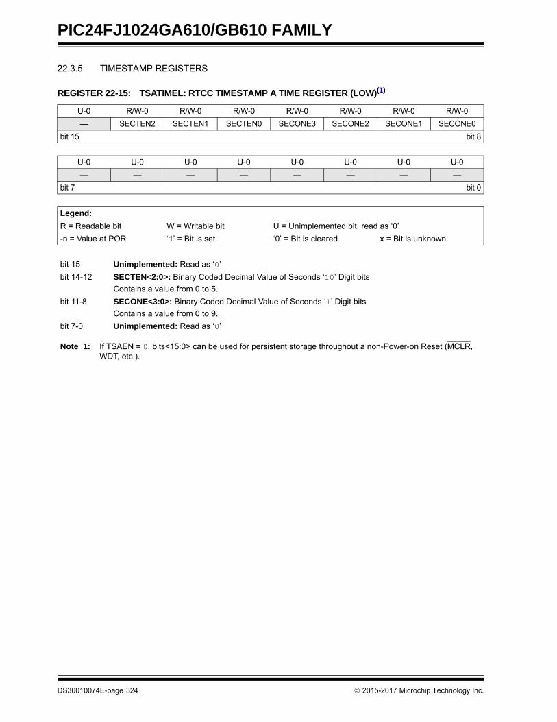
PIC24FJ1024GA610/GB610 FAMILY
22.3.5 TIMESTAMP REGISTERS
REGISTER 22-15: TSATIMEL: RTCC TIMESTAMP A TIME REGISTER (LOW)(1)
U-0 R/W-0 R/W-0 R/W-0 R/W-0 R/W-0 R/W-0 R/W-0
— SECTEN2 SECTEN1 SECTEN0 SECONE3 SECONE2 SECONE1 SECONE0
bit 15 bit 8
U-0 U-0 U-0 U-0 U-0 U-0 U-0 U-0
— — — — — — — —
bit 7 bit 0
Legend:
R = Readable bit W = Writable bit U = Unimplemented bit, read as ‘0’
-n = Value at POR ‘1’ = Bit is set ‘0’ = Bit is cleared x = Bit is unknown
bit 15 Unimplemented: Read as ‘0’
bit 14-12 SECTEN<2:0>: Binary Coded Decimal Value of Seconds ‘10’ Digit bits
Contains a value from 0 to 5.
bit 11-8 SECONE<3:0>: Binary Coded Decimal Value of Seconds ‘1’ Digit bits
Contains a value from 0 to 9.
bit 7-0 Unimplemented: Read as ‘0’
Note 1: If TSAEN = 0, bits<15:0> can be used for persistent storage throughout a non-Power-on Reset (MCLR, WDT, etc.).
DS30010074E-page 324 2015-2017 Microchip Technology Inc.

PIC24FJ1024GA610/GB610 FAMILY
REGISTER 22-16: TSATIMEH: RTCC TIMESTAMP A TIME REGISTER (HIGH)(1)
U-0 U-0 R/W-0 R/W-0 R/W-0 R/W-0 R/W-0 R/W-0
— — HRTEN1 HRTEN0 HRONE3 HRONE2 HRONE1 HRONE0
bit 15 bit 8
U-0 R/W-0 R/W-0 R/W-0 R/W-0 R/W-0 R/W-0 R/W-0
— MINTEN2 MINTEN1 MINTEN0 MINONE3 MINONE2 MINONE1 MINONE0
bit 7 bit 0
Legend:
R = Readable bit W = Writable bit U = Unimplemented bit, read as ‘0’
-n = Value at POR ‘1’ = Bit is set ‘0’ = Bit is cleared x = Bit is unknown
bit 15-14 Unimplemented: Read as ‘0’
bit 13-12 HRTEN<1:0>: Binary Coded Decimal Value of Hours ‘10’ Digit bits
Contains a value from 0 to 2.
bit 11-8 HRONE<3:0>: Binary Coded Decimal Value of Hours ‘1’ Digit bits
Contains a value from 0 to 9.
bit 7 Unimplemented: Read as ‘0’
bit 6-4 MINTEN<2:0>: Binary Coded Decimal Value of Minutes ‘10’ Digit bits
Contains a value from 0 to 5.
bit 3-0 MINONE<3:0>: Binary Coded Decimal Value of Minutes ‘1’ Digit bits
Contains a value from 0 to 9.
Note 1: If TSAEN = 0, bits<15:0> can be used for persistence storage throughout a non-Power-on Reset (MCLR, WDT, etc.).
2015-2017 Microchip Technology Inc. DS30010074E-page 325

PIC24FJ1024GA610/GB610 FAMILY
REGISTER 22-17: TSADATEL: RTCC TIMESTAMP A DATE REGISTER (LOW)(1)
U-0 U-0 R/W-0 R/W-0 R/W-0 R/W-0 R/W-0 R/W-0
— — DAYTEN1 DAYTEN0 DAYONE3 DAYONE2 DAYONE1 DAYONE0
bit 15 bit 8
U-0 U-0 U-0 U-0 U-0 R/W-0 R/W-0 R/W-0
— — — — — WDAY2 WDAY1 WDAY0
bit 7 bit 0
Legend:
R = Readable bit W = Writable bit U = Unimplemented bit, read as ‘0’
-n = Value at POR ‘1’ = Bit is set ‘0’ = Bit is cleared x = Bit is unknown
bit 15-14 Unimplemented: Read as ‘0’
bit 13-12 DAYTEN<1:0>: Binary Coded Decimal Value of Days ‘10’ Digit bits
Contains a value from 0 to 3.
bit 11-8 DAYONE<3:0>: Binary Coded Decimal Value of Days ‘1’ Digit bits
Contains a value from 0 to 9.
bit 7-3 Unimplemented: Read as ‘0’
bit 2-0 WDAY<2:0>: Binary Coded Decimal Value of Weekdays ‘1’ Digit bits
Contains a value from 0 to 6.
Note 1: If TSAEN = 0, bits<15:0> can be used for persistence storage throughout a non-Power-on Reset (MCLR, WDT, etc.).
DS30010074E-page 326 2015-2017 Microchip Technology Inc.

PIC24FJ1024GA610/GB610 FAMILY
REGISTER 22-18: TSADATEH: RTCC TIMESTAMP A DATE REGISTER (HIGH)(1)
R/W-0 R/W-0 R/W-0 R/W-0 R/W-0 R/W-0 R/W-0 R/W-0
YRTEN3 YRTEN2 YRTEN1 YRTEN0 YRONE3 YRONE2 YRONE1 YRONE0
bit 15 bit 8
U-0 U-0 U-0 R/W-0 R/W-0 R/W-0 R/W-0 R/W-0
— — — MTHTEN MTHONE3 MTHONE2 MTHONE1 MTHONE0
bit 7 bit 0
Legend:
R = Readable bit W = Writable bit U = Unimplemented bit, read as ‘0’
-n = Value at POR ‘1’ = Bit is set ‘0’ = Bit is cleared x = Bit is unknown
bit 15-12 YRTEN<3:0>: Binary Coded Decimal Value of Years ‘10’ Digit bits
bit 11-8 YRONE<3:0>: Binary Coded Decimal Value of Years ‘1’ Digit bits
bit 7-5 Unimplemented: Read as ‘0’
bit 4 MTHTEN: Binary Coded Decimal Value of Months ‘10’ Digit bit
Contains a value from 0 to 1.
bit 3-0 MTHONE<2:0>: Binary Coded Decimal Value of Months ‘1’ Digit bits
Contains a value from 0 to 9.
Note 1: If TSAEN = 0, bits<15:0> can be used for persistence storage throughout a non-Power-on Reset (MCLR, WDT, etc.).
2015-2017 Microchip Technology Inc. DS30010074E-page 327

PIC24FJ1024GA610/GB610 FAMILY
22.4 Calibration
22.4.1 CLOCK SOURCE CALIBRATION
A crystal oscillator that is connected to the RTCC maybe calibrated to provide an accurate 1 second clock intwo ways. First, coarse frequency adjustment is per-formed by adjusting the value written to the DIV<15:0>bits. Secondly, a 5-bit value can be written to theFDIV<4:0> control bits to perform a fine clock division.
The DIVx and FDIVx values can be concatenated andconsidered as a 21-bit prescaler value. If the oscillatorsource is slightly faster than ideal, the FDIV<4:0> valuecan be increased to make a small decrease in the RTCfrequency. The value of DIV<15:0> should beincreased to make larger decreases in the RTCfrequency. If the oscillator source is slower than ideal,FDIV<4:0> may be decreased for small calibrationchanges and DIV<15:0> may need to be decreased tomake larger calibration changes.
Before calibration, the user must determine the error ofthe crystal. This should be done using another timerresource on the device or an external timing reference.It is up to the user to include in the error value, the initialerror of the crystal, drift due to temperature and driftdue to crystal aging.
22.5 Alarm
• Configurable from half second to one year
• Enabled using the ALRMEN bit (RTCCON1H<15>)
• One-time alarm and repeat alarm options are available
22.5.1 CONFIGURING THE ALARM
The alarm feature is enabled using the ALRMEN bit.This bit is cleared when an alarm is issued. Writes toALRMVAL should only take place when ALRMEN = 0.
As shown in Figure 22-2, the interval selection of thealarm is configured through the AMASK<3:0> bits(RTCCON1H<11:8>). These bits determine which andhow many digits of the alarm must match the clockvalue for the alarm to occur.
The alarm can also be configured to repeat based on apreconfigured interval. The amount of times thisoccurs, once the alarm is enabled, is stored in theALMRPT<7:0> bits (RTCCON1H<7:0>). When thevalue of the ALMRPTx bits equals 00h and the CHIMEbit (RTCCON1H<14>) is cleared, the repeat function isdisabled and only a single alarm will occur. The alarmcan be repeated, up to 255 times by loadingALMRPT<7:0> with FFh.
After each alarm is issued, the value of the ALMRPTxbits is decremented by one. Once the value has reached00h, the alarm will be issued one last time, after which,the ALRMEN bit will be cleared automatically and thealarm will turn off.
Indefinite repetition of the alarm can occur if theCHIME bit = 1. Instead of the alarm being disabledwhen the value of the ALMRPTx bits reaches 00h, itrolls over to FFh and continues counting indefinitelywhile CHIME is set.
22.5.2 ALARM INTERRUPT
At every alarm event, an interrupt is generated. Thisoutput is completely synchronous to the RTCC clockand can be used as a Trigger clock to the otherperipherals.
Note: Changing any of the register bits, otherthan the RTCOE bit (RTCCON1L<7>), theALMRPT<7:0> bits (RTCCON1H<7:0>and the CHIME bit, while the alarm isenabled (ALRMEN = 1), can result in afalse alarm event leading to a false alarminterrupt. To avoid a false alarm event, thetimer and alarm values should only bechanged while the alarm is disabled(ALRMEN = 0).
DS30010074E-page 328 2015-2017 Microchip Technology Inc.
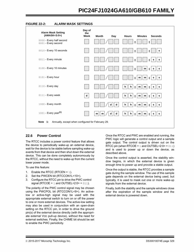
PIC24FJ1024GA610/GB610 FAMILY
FIGURE 22-2: ALARM MASK SETTINGS
22.6 Power Control
The RTCC includes a power control feature that allowsthe device to periodically wake-up an external device,wait for the device to be stable before sampling wake-upevents from that device and then shut down the externaldevice. This can be done completely autonomously bythe RTCC, without the need to wake-up from the currentlower power mode.
To use this feature:
1. Enable the RTCC (RTCEN = 1).2. Set the PWCEN bit (RTCCON1L<10>).3. Configure the RTCC pin to drive the PWC control
signal (RTCOE = 1 and OUTSEL<2:0> = 011).
The polarity of the PWC control signal may be chosenusing the PWCPOL bit (RTCCON1L<9>). An active-low or active-high signal may be used with theappropriate external switch to turn on or off the powerto one or more external devices. The active-low settingmay also be used in conjunction with an open-drainsetting on the RTCC pin, in order to drive the groundpin(s) of the external device directly (with the appropri-ate external VDD pull-up device), without the need forexternal switches. Finally, the CHIME bit should be setto enable the PWC periodicity.
Once the RTCC and PWC are enabled and running, thePWC logic will generate a control output and a samplegate output. The control output is driven out on theRTCC pin (when RTCOE = 1 and OUTSEL<2:0> = 011)and is used to power up or down the device, asdescribed above.
Once the control output is asserted, the stability win-dow begins, in which the external device is givenenough time to power up and provide a stable output.
Once the output is stable, the RTCC provides a samplegate during the sample window. The use of this samplegate depends on the external device being used, buttypically, it is used to mask out one or more wake-upsignals from the external device.
Finally, both the stability and the sample windows closeafter the expiration of the sample window and theexternal device is powered down.
Note 1: Annually, except when configured for February 29.
s
s s
m s s
m m s s
h h m m s s
d h h m m s s
d d h h m m s s
m m d d h h m m s s
Day ofthe
Week Month Day Hours Minutes Seconds
Alarm Mask Setting(AMASK<3:0>)
0000 - Every half second0001 - Every second
0010 - Every 10 seconds
0011 - Every minute
0100 - Every 10 minutes
0101 - Every hour
0110 - Every day
0111 - Every week
1000 - Every month
1001 - Every year(1)
2015-2017 Microchip Technology Inc. DS30010074E-page 329

PIC24FJ1024GA610/GB610 FAMILY
DS30010074E-page 330 2015-2017 Microchip Technology Inc.
22.6.1 POWER CONTROL CLOCK SOURCE
The stability and sample windows are controlled by thePWCSAMPx and PWCSTABx bit fields in theRTCCON3L register (RTCCON3L<15:8> and <7:0>,respectively). As both the stability and sample windowsare defined in terms of the RTCC clock, theirabsolute values vary by the value of the PWC clockbase period (TPWCCLK). For example, using a32.768 kHz SOSC input clock would produce aTPWCCLK of 1/32768 = 30.518 µs. The 8-bit magnitudeof PWCSTABx and PWCSAMPx allows for a windowsize of 0 to 255 TPWCCLK. The period of the PWC clockcan also be adjusted with a 1:1, 1:16, 1:64 or1:256 prescaler, determined by the PWCPS<1:0> bits(RTCCON2L<7:6>).
In addition, certain values for the PWCSTABx andPWCSAMPx fields have specific control meanings indetermining power control operations. If either bit field is00h, the corresponding window is inactive. In addition, ifthe PWCSTABx field is FFh, the stability windowremains active continuously, even if power control isdisabled.
22.7 Event Timestamping
The RTCC includes a set of Timestamp registers thatmay be used for the capture of Time and Date registervalues when an external input signal is received. TheRTCC will trigger a timestamp event when a low pulseoccurs on the TMPR pin.
22.7.1 TIMESTAMP OPERATION
The event input is enabled for timestamping using theTSAEN bit (RTCCON1L<0>). When the timestamp eventoccurs, the present time and date values will be stored inthe TSATIMEL/H and TSADATEL/H registers, theTSAEVT status bit (RTCSTATL<3>) will be set and anRTCC interrupt will occur. A new timestamp capture eventcannot occur until the user clears the TSAEVT status bit.
22.7.2 MANUAL TIMESTAMP OPERATION
The current time and date may be captured in theTSATIMEL/H and TSADATEL/H registers by writing a‘1’ to the TSAEVT bit location while the timestamp func-tionality is enabled (TSAEN = 1). This write will not setthe TSAEVT bit, but it will initiate a timestamp capture.The TSAEVT bit will be set when the capture operationis complete. The user must poll the TSAEVT bit todetermine when the capture operation is complete.
After the Timestamp registers have been read, theTSAEVT bit should be cleared to allow furtherhardware or software timestamp capture events.
Note 1: The TSATIMEL/H and TSADATEL/H regis-ter pairs can be used for data storage whenTSAEN = 0. The values of TSATIMEL/Hand TSADATEL/H will be maintainedthroughout all types of non-Power-onResets (MCLR, WDT, etc).

PIC24FJ1024GA610/GB610 FAMILY
23.0 32-BIT PROGRAMMABLE CYCLIC REDUNDANCY CHECK (CRC) GENERATOR
The 32-bit programmable CRC generator provides ahardware implemented method of quickly generatingchecksums for various networking and securityapplications. It offers the following features:
• User-Programmable CRC Polynomial Equation, up to 32 bits
• Programmable Shift Direction (little or big-endian)
• Independent Data and Polynomial Lengths
• Configurable Interrupt Output
• Data FIFO
Figure 23-1 displays a simplified block diagram of theCRC generator. A simple version of the CRC shiftengine is displayed in Figure 23-2.
FIGURE 23-1: CRC BLOCK DIAGRAM
FIGURE 23-2: CRC SHIFT ENGINE DETAIL
Note: This data sheet summarizes the features ofthis group of PIC24F devices. It is notintended to be a comprehensive referencesource. For more information, refer tothe “dsPIC33/PIC24 Family ReferenceManual”, “32-Bit ProgrammableCyclic Redundancy Check (CRC)”(DS30009729), which is available from theMicrochip web site (www.microchip.com).The information in this data sheetsupersedes the information in the FRM.
CRCInterrupt
Variable FIFO(4x32, 8x16 or 16x8)
CRCDATH CRCDATL
Shift BufferCRC Shift Engine
CRCWDATH CRCWDATL
Shifter Clock2 * FCY
LENDIAN
CRCISEL
1
0
FIFO EmptyEvent
ShiftComplete
Event
1
0
Note 1: n = PLEN<4:0> + 1.
CRC Shift Engine CRCWDATH CRCWDATL
Bit 1
X0 X1 Xn(1)
Read/Write Bus
Shift BufferData Bit 0 Bit n(1)
2015-2017 Microchip Technology Inc. DS30010074E-page 331
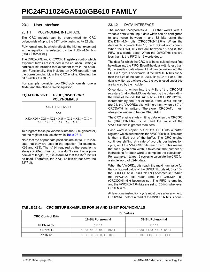
PIC24FJ1024GA610/GB610 FAMILY
23.1 User Interface
23.1.1 POLYNOMIAL INTERFACE
The CRC module can be programmed for CRCpolynomials of up to the 32nd order, using up to 32 bits.
Polynomial length, which reflects the highest exponentin the equation, is selected by the PLEN<4:0> bits(CRCCON2<4:0>).
The CRCXORL and CRCXORH registers control whichexponent terms are included in the equation. Setting aparticular bit includes that exponent term in the equa-tion. Functionally, this includes an XOR operation onthe corresponding bit in the CRC engine. Clearing thebit disables the XOR.
For example, consider two CRC polynomials, one a16-bit and the other a 32-bit equation.
EQUATION 23-1: 16-BIT, 32-BIT CRC POLYNOMIALS
To program these polynomials into the CRC generator,set the register bits, as shown in Table 23-1.
Note that the appropriate positions are set to ‘1’ to indi-cate that they are used in the equation (for example,X26 and X23). The ‘0’ bit required by the equation isalways XORed; thus, X0 is a don’t care. For a poly-nomial of length 32, it is assumed that the 32nd bit willbe used. Therefore, the X<31:1> bits do not have the32nd bit.
23.1.2 DATA INTERFACE
The module incorporates a FIFO that works with avariable data width. Input data width can be configuredto any value between 1 and 32 bits using theDWIDTH<4:0> bits (CRCCON2<12:8>). When thedata width is greater than 15, the FIFO is 4 words deep.When the DWIDTHx bits are between 15 and 8, theFIFO is 8 words deep. When the DWIDTHx bits areless than 8, the FIFO is 16 words deep.
The data for which the CRC is to be calculated must firstbe written into the FIFO. Even if the data width is less than8, the smallest data element that can be written into theFIFO is 1 byte. For example, if the DWIDTHx bits are 5,then the size of the data is DWIDTH<4:0> + 1 or 6. Thedata is written as a whole byte; the two unused upper bitsare ignored by the module.
Once data is written into the MSb of the CRCDATregisters (that is, the MSb as defined by the data width),the value of the VWORD<4:0> bits (CRCCON1<12:8>)increments by one. For example, if the DWIDTHx bitsare 24, the VWORDx bits will increment when bit 7 ofCRCDATH is written. Therefore, CRCDATL mustalways be written to before CRCDATH.
The CRC engine starts shifting data when the CRCGObit (CRCCON1<4>) is set and the value of theVWORDx bits is greater than zero.
Each word is copied out of the FIFO into a bufferregister, which decrements the VWORDx bits. The datais then shifted out of the buffer. The CRC enginecontinues shifting at a rate of two bits per instructioncycle, until the VWORDx bits reach zero. This meansthat for a given data width, it takes half that number ofinstructions for each word to complete the calculation.For example, it takes 16 cycles to calculate the CRC fora single word of 32-bit data.
When the VWORDx bits reach the maximum value forthe configured value of the DWIDTHx bits (4, 8 or 16),the CRCFUL bit (CRCCON1<7>) becomes set. Whenthe VWORDx bits reach zero, the CRCMPT bit(CRCCON1<6>) becomes set. The FIFO is emptiedand the VWORD<4:0> bits are set to ‘00000’ wheneverCRCEN is ‘0’.
At least one instruction cycle must pass after a write toCRCWDAT before a read of the VWORDx bits is done.
and
X32+X26 + X23 + X22 + X16 + X12 + X11 + X10 +X8 + X7 + X5 + X4 + X2 + X + 1
X16 + X12 + X5 + 1
TABLE 23-1: CRC SETUP EXAMPLES FOR 16 AND 32-BIT POLYNOMIALS
CRC Control BitsBit Values
16-Bit Polynomial 32-Bit Polynomial
PLEN<4:0> 01111 11111
X<31:16> 0000 0000 0000 0001 0000 0100 1100 0001
X<15:1> 0001 0000 0010 000 0001 1101 1011 011
DS30010074E-page 332 2015-2017 Microchip Technology Inc.

PIC24FJ1024GA610/GB610 FAMILY
23.1.3 DATA SHIFT DIRECTION
The LENDIAN bit (CRCCON1<3>) is used to controlthe shift direction. By default, the CRC will shift datathrough the engine, MSb first. Setting LENDIAN (= 1)causes the CRC to shift data, LSb first. This settingallows better integration with various communicationschemes and removes the overhead of reversing thebit order in software. Note that this only changes thedirection the data is shifted into the engine. The resultof the CRC calculation will still be a normal CRC result,not a reverse CRC result.
23.1.4 INTERRUPT OPERATION
The module generates an interrupt that is configurableby the user for either of two conditions.
If CRCISEL is ‘0’, an interrupt is generated when theVWORD<4:0> bits make a transition from a value of ‘1’to ‘0’. If CRCISEL is ‘1’, an interrupt will be generatedafter the CRC operation finishes and the module setsthe CRCGO bit to ‘0’. Manually setting CRCGO to ‘0’will not generate an interrupt. Note that when aninterrupt occurs, the CRC calculation would not yet becomplete. The module will still need (PLENx + 1)/2clock cycles after the interrupt is generated until theCRC calculation is finished.
23.1.5 TYPICAL OPERATION
To use the module for a typical CRC calculation:
1. Set the CRCEN bit to enable the module.
2. Configure the module for desired operation:a) Program the desired polynomial using the
CRCXOR registers and PLEN<4:0> bits.
b) Configure the data width and shift directionusing the DWIDTH<4:0> and LENDIAN bits.
3. Set the CRCGO bit to start the calculations.
4. Set the desired CRC non-direct initial value bywriting to the CRCWDAT registers.
5. Load all data into the FIFO by writing to theCRCDAT registers as space becomes available(the CRCFUL bit must be zero before the nextdata loading).
6. Wait until the data FIFO is empty (CRCMPT bitis set).
7. Read the result:If the data width (DWIDTH<4:0> bits) is morethan the polynomial length (PLEN<4:0> bits):a) Wait (DWIDTH<4:0> + 1)/2 instruction cycles
to make sure that shifts from the shift bufferare finished.
b) Change the data width to the polynomiallength (DWIDTH<4:0> = PLEN<4:0>).
c) Write one dummy data word to the CRCDATregisters.
d) Wait 2 instruction cycles to move the datafrom the FIFO to the shift buffer and(PLEN<4:0> + 1)/2 instruction cycles toshift out the result.
Or, if the data width (DWIDTH<4:0> bits) is less thanthe polynomial length (PLEN<4:0> bits):
1. Clear the CRC Interrupt Selection bit(CRCISEL = 0) to get the interrupt when allshifts are done. Clear the CRC interrupt flag.Write dummy data in the CRCDAT registers andwait until the CRC interrupt flag is set.
2. Read the final CRC result from the CRCWDATregisters.
3. Restore the data width (DWIDTH<4:0> bits) forfurther calculations (OPTIONAL). If the datawidth (DWIDTH<4:0> bits) is equal to, or lessthan, the polynomial length (PLEN<4:0> bits):
a) Clear the CRC Interrupt Selection bit(CRCISEL = 0) to get the interrupt when allshifts are done.
b) Suspend the calculation by settingCRCGO = 0.
c) Clear the CRC interrupt flag.
d) Write the dummy data with the total datalength equal to the polynomial length in theCRCDAT registers.
e) Resume the calculation by settingCRCGO = 1.
f) Wait until the CRC interrupt flag is set.
g) Read the final CRC result from theCRCWDAT registers.
There are eight registers used to control programmableCRC operation:
• CRCCON1
• CRCCON2
• CRCXORL
• CRCXORH
• CRCDATL
• CRCDATH
• CRCWDATL
• CRCWDATH
The CRCCON1 and CRCCON2 registers (Register 23-1and Register 23-2) control the operation of the moduleand configure the various settings.
The CRCXOR registers (Register 23-3 andRegister 23-4) select the polynomial terms to be usedin the CRC equation. The CRCDAT and CRCWDATregisters are each register pairs that serve as buffersfor the double-word input data, and CRC processedoutput, respectively.
2015-2017 Microchip Technology Inc. DS30010074E-page 333

PIC24FJ1024GA610/GB610 FAMILY
REGISTER 23-1: CRCCON1: CRC CONTROL 1 REGISTER
R/W-0 U-0 R/W-0 R-0, HSC R-0, HSC R-0, HSC R-0, HSC R-0, HSC
CRCEN — CSIDL VWORD4 VWORD3 VWORD2 VWORD1 VWORD0
bit 15 bit 8
R-0, HSC R-1, HSC R/W-0 R/W-0, HC R/W-0 U-0 U-0 U-0
CRCFUL CRCMPT CRCISEL CRCGO LENDIAN — — —
bit 7 bit 0
Legend: HC = Hardware Clearable bit HSC = Hardware Settable/Clearable bit
R = Readable bit W = Writable bit U = Unimplemented bit, read as ‘0’
-n = Value at POR ‘1’ = Bit is set ‘0’ = Bit is cleared x = Bit is unknown
bit 15 CRCEN: CRC Enable bit
1 = Enables module0 = Disables module; all state machines, pointers and CRCWDAT/CRCDATH registers reset; other
SFRs are NOT reset
bit 14 Unimplemented: Read as ‘0’
bit 13 CSIDL: CRC Stop in Idle Mode bit
1 = Discontinues module operation when device enters Idle mode0 = Continues module operation in Idle mode
bit 12-8 VWORD<4:0>: CRC Pointer Value bits
Indicates the number of valid words in the FIFO. Has a maximum value of 8 when PLEN<4:0> 7 or 16when PLEN<4:0> 7.
bit 7 CRCFUL: CRC FIFO Full bit
1 = FIFO is full 0 = FIFO is not full
bit 6 CRCMPT: CRC FIFO Empty bit
1 = FIFO is empty 0 = FIFO is not empty
bit 5 CRCISEL: CRC Interrupt Selection bit
1 = Interrupt on FIFO is empty; the final word of data is still shifting through the CRC0 = Interrupt on shift is complete and results are ready
bit 4 CRCGO: Start CRC bit
1 = Starts CRC serial shifter0 = CRC serial shifter is turned off
bit 3 LENDIAN: Data Shift Direction Select bit
1 = Data word is shifted into the CRC, starting with the LSb (little-endian)0 = Data word is shifted into the CRC, starting with the MSb (big-endian)
bit 2-0 Unimplemented: Read as ‘0’
DS30010074E-page 334 2015-2017 Microchip Technology Inc.

PIC24FJ1024GA610/GB610 FAMILY
REGISTER 23-2: CRCCON2: CRC CONTROL 2 REGISTER
U-0 U-0 U-0 R/W-0 R/W-0 R/W-0 R/W-0 R/W-0
— — — DWIDTH4 DWIDTH3 DWIDTH2 DWIDTH1 DWIDTH0
bit 15 bit 8
U-0 U-0 U-0 R/W-0 R/W-0 R/W-0 R/W-0 R/W-0
— — — PLEN4 PLEN3 PLEN2 PLEN1 PLEN0
bit 7 bit 0
Legend:
R = Readable bit W = Writable bit U = Unimplemented bit, read as ‘0’
-n = Value at POR ‘1’ = Bit is set ‘0’ = Bit is cleared x = Bit is unknown
bit 15-13 Unimplemented: Read as ‘0’
bit 12-8 DWIDTH<4:0>: CRC Data Word Width Configuration bits
Configures the width of the data word (Data Word Width – 1).
bit 7-5 Unimplemented: Read as ‘0’
bit 4-0 PLEN<4:0>: Polynomial Length Configuration bits
Configures the length of the polynomial (Polynomial Length – 1).
2015-2017 Microchip Technology Inc. DS30010074E-page 335

PIC24FJ1024GA610/GB610 FAMILY
REGISTER 23-3: CRCXORL: CRC XOR POLYNOMIAL REGISTER, LOW BYTE
R/W-0 R/W-0 R/W-0 R/W-0 R/W-0 R/W-0 R/W-0 R/W-0
X<15:8>
bit 15 bit 8
R/W-0 R/W-0 R/W-0 R/W-0 R/W-0 R/W-0 R/W-0 U-0
X<7:1> —
bit 7 bit 0
Legend:
R = Readable bit W = Writable bit U = Unimplemented bit, read as ‘0’
-n = Value at POR ‘1’ = Bit is set ‘0’ = Bit is cleared x = Bit is unknown
bit 15-1 X<15:1>: XOR of Polynomial Term xn Enable bits
bit 0 Unimplemented: Read as ‘0’
REGISTER 23-4: CRCXORH: CRC XOR POLYNOMIAL REGISTER, HIGH BYTE
R/W-0 R/W-0 R/W-0 R/W-0 R/W-0 R/W-0 R/W-0 R/W-0
X<31:24>
bit 15 bit 8
R/W-0 R/W-0 R/W-0 R/W-0 R/W-0 R/W-0 R/W-0 R/W-0
X<23:16>
bit 7 bit 0
Legend:
R = Readable bit W = Writable bit U = Unimplemented bit, read as ‘0’
-n = Value at POR ‘1’ = Bit is set ‘0’ = Bit is cleared x = Bit is unknown
bit 15-0 X<31:16>: XOR of Polynomial Term xn Enable bits
DS30010074E-page 336 2015-2017 Microchip Technology Inc.
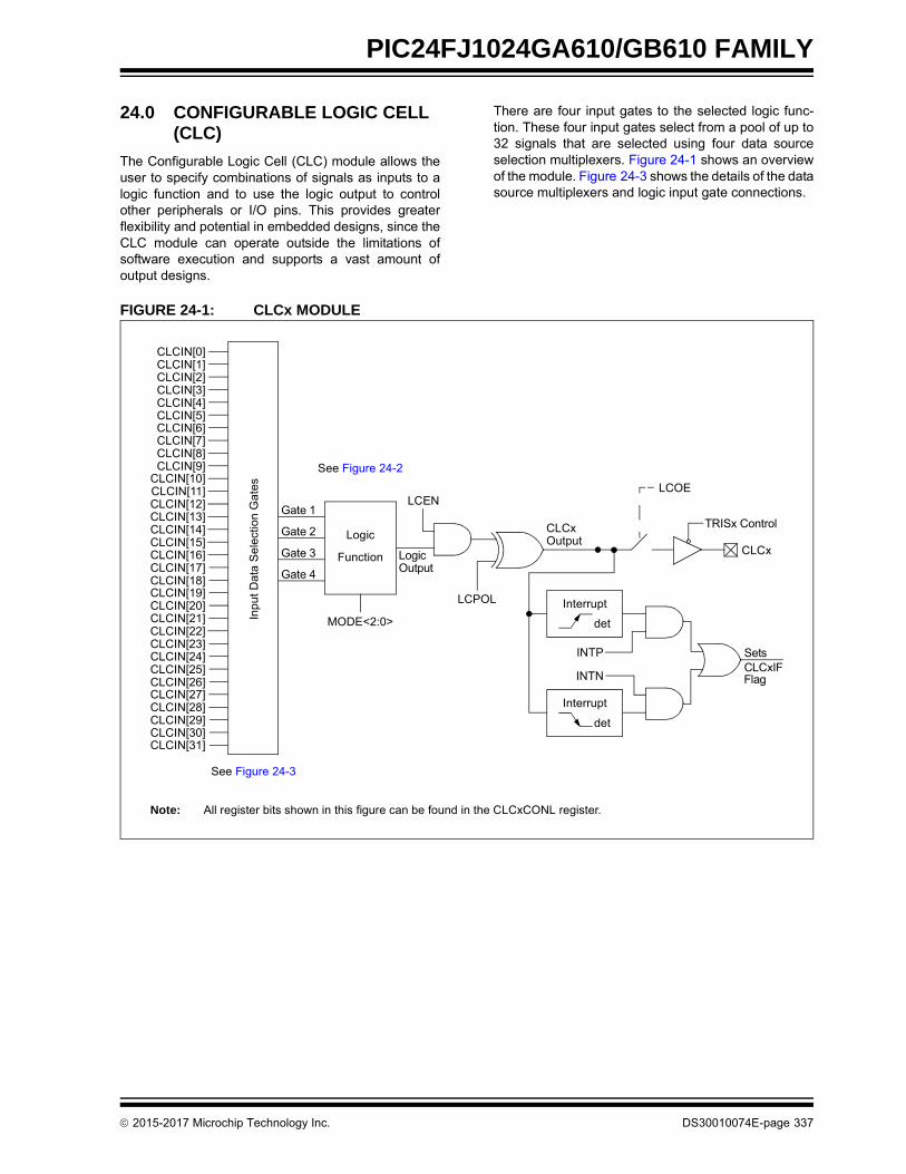
PIC24FJ1024GA610/GB610 FAMILY
24.0 CONFIGURABLE LOGIC CELL (CLC)
The Configurable Logic Cell (CLC) module allows theuser to specify combinations of signals as inputs to alogic function and to use the logic output to controlother peripherals or I/O pins. This provides greaterflexibility and potential in embedded designs, since theCLC module can operate outside the limitations ofsoftware execution and supports a vast amount ofoutput designs.
There are four input gates to the selected logic func-tion. These four input gates select from a pool of up to32 signals that are selected using four data sourceselection multiplexers. Figure 24-1 shows an overviewof the module. Figure 24-3 shows the details of the datasource multiplexers and logic input gate connections.
FIGURE 24-1: CLCx MODULE
Gate 1
Gate 2
Gate 3
Gate 4
Logic
Function
Inp
ut
Da
ta S
ele
ctio
n G
ate
s
CLCx
LCOE
Logic
LCPOL
MODE<2:0>
CLCx
CLCIN[0]CLCIN[1]CLCIN[2]CLCIN[3]CLCIN[4]CLCIN[5]CLCIN[6]CLCIN[7]CLCIN[8]CLCIN[9]
CLCIN[10]CLCIN[11]CLCIN[12]CLCIN[13]CLCIN[14]CLCIN[15]
TRISx Control
Interrupt
det
INTP
INTN
LCEN
CLCxIFSets
Flag
Note: All register bits shown in this figure can be found in the CLCxCONL register.
Output
OutputCLCIN[16]CLCIN[17]CLCIN[18]CLCIN[19]CLCIN[20]CLCIN[21]CLCIN[22]CLCIN[23]CLCIN[24]CLCIN[25]CLCIN[26]CLCIN[27]CLCIN[28]CLCIN[29]CLCIN[30]CLCIN[31]
See Figure 24-2
See Figure 24-3
Interrupt
det
2015-2017 Microchip Technology Inc. DS30010074E-page 337

PIC24FJ1024GA610/GB610 FAMILY
FIGURE 24-2: CLCx LOGIC FUNCTION COMBINATORIAL OPTIONS
Gate 1
Gate 2
Gate 3
Gate 4
Logic Output
Gate 1
Gate 2
Gate 3
Gate 4
Logic Output
Gate 1
Gate 2
Gate 3
Gate 4
Logic Output
S
R
QGate 1
Gate 2
Gate 3
Gate 4
Logic Output
D Q
Gate 1
Gate 2
Gate 3
Gate 4
Logic OutputS
R
J QGate 2
Gate 3
Gate 4
Logic Output
R
Gate 1
K
D Q
Gate 1
Gate 2
Gate 3
Gate 4
Logic OutputS
R
D Q
Gate 1
Gate 3
Logic Output
R
Gate 4
Gate 2
MODE<2:0> = 000
MODE<2:0> = 010
MODE<2:0> = 001
MODE<2:0> = 011
MODE<2:0> = 100
MODE<2:0> = 110
MODE<2:0> = 101
MODE<2:0> = 111
LE
AND – OR OR – XOR
4-Input AND S-R Latch
1-Input D Flip-Flop with S and R 2-Input D Flip-Flop with R
1-Input Transparent Latch with S and RJ-K Flip-Flop with R
DS30010074E-page 338 2015-2017 Microchip Technology Inc.

PIC24FJ1024GA610/GB610 FAMILY
FIGURE 24-3: CLCx INPUT SOURCE SELECTION DIAGRAM
Gate 1
G1POL
Data Gate 1
G1D1T
Gate 2
Gate 3
Gate 4
Data Gate 2
Data Gate 3
Data Gate 4
G1D1N
DS1x (CLCxSEL<2:0>)
DS2x (CLCxSEL<6:4>)
CLCIN[0]CLCIN[1]CLCIN[2]
CLCIN[5]CLCIN[6]CLCIN[7]
Data Selection
Note: All controls are undefined at power-up.
Data 1 Non-Inverted
Data 1
Data 2 Non-Inverted
Data 2
Data 3 Non-Inverted
Data 3
Data 4 Non-Inverted
Data 4
(Same as Data Gate 1)
(Same as Data Gate 1)
(Same as Data Gate 1)
G1D2T
G1D2N
G1D3T
G1D3N
G1D4T
G1D4N
Inverted
Inverted
Inverted
Inverted
CLCIN[8]CLCIN[9]
CLCIN[10]
CLCIN[13]CLCIN[14]CLCIN[15]
CLCIN[3]CLCIN[4]
CLCIN[11]CLCIN[12]
CLCIN[18]
CLCIN[21]CLCIN[22]CLCIN[23]
CLCIN[19]CLCIN[20]
CLCIN[17]CLCIN[16]
DS3x (CLCxSEL<10:8>)
CLCIN[26]
CLCIN[29]CLCIN[30]CLCIN[31]
CLCIN[27]CLCIN[28]
CLCIN[25]CLCIN[24]
DS4x (CLCxSEL<14:12>)
000
111
000
111
000
111
000
111
(CLCxCONH<0>)
2015-2017 Microchip Technology Inc. DS30010074E-page 339

PIC24FJ1024GA610/GB610 FAMILY
24.1 Control Registers
The CLCx module is controlled by the following registers:
• CLCxCONL
• CLCxCONH
• CLCxSEL
• CLCxGLSL
• CLCxGLSH
The CLCx Control registers (CLCxCONL andCLCxCONH) are used to enable the module and inter-rupts, control the output enable bit, select output polarityand select the logic function. The CLCx Control registersalso allow the user to control the logic polarity of not onlythe cell output, but also some intermediate variables.
The CLCx Input MUX Select register (CLCxSEL)allows the user to select up to 4 data input sourcesusing the 4 data input selection multiplexers. Eachmultiplexer has a list of 8 data sources available.
The CLCx Gate Logic Input Select registers (CLCxGLSLand CLCxGLSH) allow the user to select which outputsfrom each of the selection MUXes are used as inputs tothe input gates of the logic cell. Each data source MUXoutputs both a true and a negated version of its output.All of these 8 signals are enabled, ORed together by thelogic cell input gates.
REGISTER 24-1: CLCxCONL: CLCx CONTROL REGISTER (LOW)
R/W-0 U-0 U-0 U-0 R/W-0 R/W-0 U-0 U-0
LCEN — — — INTP INTN — —
bit 15 bit 8
R/W-0 R-0 R/W-0 U-0 U-0 R/W-0 R/W-0 R/W-0
LCOE LCOUT LCPOL — — MODE2 MODE1 MODE0
bit 7 bit 0
Legend:
R = Readable bit W = Writable bit U = Unimplemented bit, read as ‘0’
-n = Value at POR ‘1’ = Bit is set ‘0’ = Bit is cleared x = Bit is unknown
bit 15 LCEN: CLCx Enable bit
1 = CLCx is enabled and mixing input signals0 = CLCx is disabled and has logic zero outputs
bit 14-12 Unimplemented: Read as ‘0’
bit 11 INTP: CLCx Positive Edge Interrupt Enable bit
1 = Interrupt will be generated when a rising edge occurs on LCOUT0 = Interrupt will not be generated
bit 10 INTN: CLCx Negative Edge Interrupt Enable bit
1 = Interrupt will be generated when a falling edge occurs on LCOUT0 = Interrupt will not be generated
bit 9-8 Unimplemented: Read as ‘0’
bit 7 LCOE: CLCx Port Enable bit
1 = CLCx port pin output is enabled0 = CLCx port pin output is disabled
bit 6 LCOUT: CLCx Data Output Status bit
1 = CLCx output high0 = CLCx output low
bit 5 LCPOL: CLCx Output Polarity Control bit
1 = The output of the module is inverted0 = The output of the module is not inverted
bit 4-3 Unimplemented: Read as ‘0’
DS30010074E-page 340 2015-2017 Microchip Technology Inc.

PIC24FJ1024GA610/GB610 FAMILY
bit 2-0 MODE<2:0>: CLCx Mode bits
111 = Cell is a 1-input transparent latch with S and R110 = Cell is a JK flip-flop with R101 = Cell is a 2-input D flip-flop with R100 = Cell is a 1-input D flip-flop with S and R011 = Cell is an SR latch010 = Cell is a 4-input AND001 = Cell is an OR-XOR000 = Cell is a AND-OR
REGISTER 24-1: CLCxCONL: CLCx CONTROL REGISTER (LOW) (CONTINUED)
REGISTER 24-2: CLCxCONH: CLCx CONTROL REGISTER (HIGH)
U-0 U-0 U-0 U-0 U-0 U-0 U-0 U-0
— — — — — — — —
bit 15 bit 8
U-0 U-0 U-0 U-0 R/W-0 R/W-0 R/W-0 R/W-0
— — — — G4POL G3POL G2POL G1POL
bit 7 bit 0
Legend:
R = Readable bit W = Writable bit U = Unimplemented bit, read as ‘0’
-n = Value at POR ‘1’ = Bit is set ‘0’ = Bit is cleared x = Bit is unknown
bit 15-4 Unimplemented: Read as ‘0’
bit 3 G4POL: Gate 4 Polarity Control bit
1 = The output of Channel 4 logic is inverted when applied to the logic cell0 = The output of Channel 4 logic is not inverted
bit 2 G3POL: Gate 3 Polarity Control bit
1 = The output of Channel 3 logic is inverted when applied to the logic cell0 = The output of Channel 3 logic is not inverted
bit 1 G2POL: Gate 2 Polarity Control bit
1 = The output of Channel 2 logic is inverted when applied to the logic cell0 = The output of Channel 2 logic is not inverted
bit 0 G1POL: Gate 1 Polarity Control bit
1 = The output of Channel 1 logic is inverted when applied to the logic cell0 = The output of Channel 1 logic is not inverted
2015-2017 Microchip Technology Inc. DS30010074E-page 341

PIC24FJ1024GA610/GB610 FAMILY
REGISTER 24-3: CLCxSEL: CLCx INPUT MUX SELECT REGISTER
U-0 R/W-0 R/W-0 R/W-0 U-0 R/W-0 R/W-0 R/W-0
— DS4<2:0> — DS3<2:0>
bit 15 bit 8
U-0 R/W-0 R/W-0 R/W-0 U-0 R/W-0 R/W-0 R/W-0
— DS2<2:0> — DS1<2:0>
bit 7 bit 0
Legend:
R = Readable bit W = Writable bit U = Unimplemented bit, read as ‘0’
-n = Value at POR ‘1’ = Bit is set ‘0’ = Bit is cleared x = Bit is unknown
bit 15 Unimplemented: Read as ‘0’
bit 14-12 DS4<2:0>: Data Selection MUX 4 Signal Selection bits
111 = MCCP3 Compare Event Interrupt Flag (CCP3IF)110 = MCCP1 Compare Event Interrupt Flag (CCP1IF)101 = Unimplemented100 = CTMU A/D Trigger011 = SPIx Input (SDIx) corresponding to the CLCx module (see Table 24-1)010 = Comparator 3 output001 = Module-specific CLCx output (see Table 24-1)000 = CLCINB I/O pin
bit 11 Unimplemented: Read as ‘0’
bit 10-8 DS3<2:0>: Data Selection MUX 3 Signal Selection bits
111 = MCCP3 Compare Event Interrupt Flag (CCP3IF)110 = MCCP2 Compare Event Interrupt Flag (CCP2IF)101 = DMA Channel 1 interrupt100 = UARTx RX output corresponding to the CLCx module (see Table 24-1)011 = SPIx Output (SDOx) corresponding to the CLCx module (see Table 24-1)010 = Comparator 2 output001 = CLCx output (see Table 24-1)000 = CLCINA I/O pin
bit 7 Unimplemented: Read as ‘0’
bit 6-4 DS2<2:0>: Data Selection MUX 2 Signal Selection bits
111 = MCCP2 Compare Event Interrupt Flag (CCP2IF)110 = MCCP1 Compare Event Interrupt Flag (CCP1IF)101 = DMA Channel 0 interrupt100 = A/D conversion done interrupt011 = UARTx TX input corresponding to the CLCx module (see Table 24-1)010 = Comparator 1 output001 = CLCx output (see Table 24-1)000 = CLCINB I/O pin
bit 3 Unimplemented: Read as ‘0’
bit 2-0 DS1<2:0>: Data Selection MUX 1 Signal Selection bits
111 = Timer3 match event110 = Timer2 match event101 = Unimplemented100 = REFO output011 = INTRC/LPRC clock source010 = SOSC clock source001 = System clock (TCY)000 = CLCINA I/O pin
DS30010074E-page 342 2015-2017 Microchip Technology Inc.

PIC24FJ1024GA610/GB610 FAMILY
TABLE 24-1: MODULE-SPECIFIC INPUT DATA SOURCES
Bit Field ValueInput Source
CLC1 CLC2 CLC3 CLC4
DS4<2:0> 011 SDI1 SDI2 SDI3 Unimplemented
001 CLC2 Output CLC1 Output CLC4 Output CLC3 Output
DS3<2:0> 100 U1RX U2RX U3RX U4RX
011 SDO1 SDO2 SDO3 Unimplemented
001 CLC1 Output CLC2 Output CLC3 Output CLC4 Output
DS2<2:0> 011 U1TX U2TX U3TX U4TX
001 CLC2 Output CLC1 Output CLC4 Output CLC3 Output
REGISTER 24-4: CLCxGLSL: CLCx GATE LOGIC INPUT SELECT LOW REGISTER
R/W-0 R/W-0 R/W-0 R/W-0 R/W-0 R/W-0 R/W-0 R/W-0
G2D4T G2D4N G2D3T G2D3N G2D2T G2D2N G2D1T G2D1N
bit 15 bit 8
R/W-0 R/W-0 R/W-0 R/W-0 R/W-0 R/W-0 R/W-0 R/W-0
G1D4T G1D4N G1D3T G1D3N G1D2T G1D2N G1D1T G1D1N
bit 7 bit 0
Legend:
R = Readable bit W = Writable bit U = Unimplemented bit, read as ‘0’
-n = Value at POR ‘1’ = Bit is set ‘0’ = Bit is cleared x = Bit is unknown
bit 15 G2D4T: Gate 2 Data Source 4 True Enable bit
1 = The Data Source 4 signal is enabled for Gate 20 = The Data Source 4 signal is disabled for Gate 2
bit 14 G2D4N: Gate 2 Data Source 4 Negated Enable bit
1 = The Data Source 4 inverted signal is enabled for Gate 20 = The Data Source 4 inverted signal is disabled for Gate 2
bit 13 G2D3T: Gate 2 Data Source 3 True Enable bit
1 = The Data Source 3 signal is enabled for Gate 20 = The Data Source 3 signal is disabled for Gate 2
bit 12 G2D3N: Gate 2 Data Source 3 Negated Enable bit
1 = The Data Source 3 inverted signal is enabled for Gate 20 = The Data Source 3 inverted signal is disabled for Gate 2
bit 11 G2D2T: Gate 2 Data Source 2 True Enable bit
1 = The Data Source 2 signal is enabled for Gate 20 = The Data Source 2 signal is disabled for Gate 2
bit 10 G2D2N: Gate 2 Data Source 2 Negated Enable bit
1 = The Data Source 2 inverted signal is enabled for Gate 20 = The Data Source 2 inverted signal is disabled for Gate 2
bit 9 G2D1T: Gate 2 Data Source 1 True Enable bit
1 = The Data Source 1 signal is enabled for Gate 20 = The Data Source 1 signal is disabled for Gate 2
2015-2017 Microchip Technology Inc. DS30010074E-page 343
PIC24FJ1024GA610/GB610 FAMILY
bit 8 G2D1N: Gate 2 Data Source 1 Negated Enable bit
1 = The Data Source 1 inverted signal is enabled for Gate 20 = The Data Source 1 inverted signal is disabled for Gate 2
bit 7 G1D4T: Gate 1 Data Source 4 True Enable bit
1 = The Data Source 4 signal is enabled for Gate 10 = The Data Source 4 signal is disabled for Gate 1
bit 6 G1D4N: Gate 1 Data Source 4 Negated Enable bit
1 = The Data Source 4 inverted signal is enabled for Gate 10 = The Data Source 4 inverted signal is disabled for Gate 1
bit 5 G1D3T: Gate 1 Data Source 3 True Enable bit
1 = The Data Source 3 signal is enabled for Gate 10 = The Data Source 3 signal is disabled for Gate 1
bit 4 G1D3N: Gate 1 Data Source 3 Negated Enable bit
1 = The Data Source 3 inverted signal is enabled for Gate 10 = The Data Source 3 inverted signal is disabled for Gate 1
bit 3 G1D2T: Gate 1 Data Source 2 True Enable bit
1 = The Data Source 2 signal is enabled for Gate 10 = The Data Source 2 signal is disabled for Gate 1
bit 2 G1D2N: Gate 1 Data Source 2 Negated Enable bit
1 = The Data Source 2 inverted signal is enabled for Gate 10 = The Data Source 2 inverted signal is disabled for Gate 1
bit 1 G1D1T: Gate 1 Data Source 1 True Enable bit
1 = The Data Source 1 signal is enabled for Gate 10 = The Data Source 1 signal is disabled for Gate 1
bit 0 G1D1N: Gate 1 Data Source 1 Negated Enable bit
1 = The Data Source 1 inverted signal is enabled for Gate 10 = The Data Source 1 inverted signal is disabled for Gate 1
REGISTER 24-4: CLCxGLSL: CLCx GATE LOGIC INPUT SELECT LOW REGISTER (CONTINUED)
DS30010074E-page 344 2015-2017 Microchip Technology Inc.

PIC24FJ1024GA610/GB610 FAMILY
REGISTER 24-5: CLCxGLSH: CLCx GATE LOGIC INPUT SELECT HIGH REGISTER
R/W-0 R/W-0 R/W-0 R/W-0 R/W-0 R/W-0 R/W-0 R/W-0
G4D4T G4D4N G4D3T G4D3N G4D2T G4D2N G4D1T G4D1N
bit 15 bit 8
R/W-0 R/W-0 R/W-0 R/W-0 R/W-0 R/W-0 R/W-0 R/W-0
G3D4T G3D4N G3D3T G3D3N G3D2T G3D2N G3D1T G3D1N
bit 7 bit 0
Legend:
R = Readable bit W = Writable bit U = Unimplemented bit, read as ‘0’
-n = Value at POR ‘1’ = Bit is set ‘0’ = Bit is cleared x = Bit is unknown
bit 15 G4D4T: Gate 4 Data Source 4 True Enable bit
1 = The Data Source 4 signal is enabled for Gate 40 = The Data Source 4 signal is disabled for Gate 4
bit 14 G4D4N: Gate 4 Data Source 4 Negated Enable bit
1 = The Data Source 4 inverted signal is enabled for Gate 40 = The Data Source 4 inverted signal is disabled for Gate 4
bit 13 G4D3T: Gate 4 Data Source 3 True Enable bit
1 = The Data Source 3 signal is enabled for Gate 40 = The Data Source 3 signal is disabled for Gate 4
bit 12 G4D3N: Gate 4 Data Source 3 Negated Enable bit
1 = The Data Source 3 inverted signal is enabled for Gate 40 = The Data Source 3 inverted signal is disabled for Gate 4
bit 11 G4D2T: Gate 4 Data Source 2 True Enable bit
1 = The Data Source 2 signal is enabled for Gate 40 = The Data Source 2 signal is disabled for Gate 4
bit 10 G4D2N: Gate 4 Data Source 2 Negated Enable bit
1 = The Data Source 2 inverted signal is enabled for Gate 40 = The Data Source 2 inverted signal is disabled for Gate 4
bit 9 G4D1T: Gate 4 Data Source 1 True Enable bit
1 = The Data Source 1 signal is enabled for Gate 40 = The Data Source 1 signal is disabled for Gate 4
bit 8 G4D1N: Gate 4 Data Source 1 Negated Enable bit
1 = The Data Source 1 inverted signal is enabled for Gate 40 = The Data Source 1 inverted signal is disabled for Gate 4
bit 7 G3D4T: Gate 3 Data Source 4 True Enable bit
1 = The Data Source 4 signal is enabled for Gate 30 = The Data Source 4 signal is disabled for Gate 3
bit 6 G3D4N: Gate 3 Data Source 4 Negated Enable bit
1 = The Data Source 4 inverted signal is enabled for Gate 30 = The Data Source 4 inverted signal is disabled for Gate 3
bit 5 G3D3T: Gate 3 Data Source 3 True Enable bit
1 = The Data Source 3 signal is enabled for Gate 30 = The Data Source 3 signal is disabled for Gate 3
bit 4 G3D3N: Gate 3 Data Source 3 Negated Enable bit
1 = The Data Source 3 inverted signal is enabled for Gate 30 = The Data Source 3 inverted signal is disabled for Gate 3
2015-2017 Microchip Technology Inc. DS30010074E-page 345

PIC24FJ1024GA610/GB610 FAMILY
bit 3 G3D2T: Gate 3 Data Source 2 True Enable bit
1 = The Data Source 2 signal is enabled for Gate 30 = The Data Source 2 signal is disabled for Gate 3
bit 2 G3D2N: Gate 3 Data Source 2 Negated Enable bit
1 = The Data Source 2 inverted signal is enabled for Gate 30 = The Data Source 2 inverted signal is disabled for Gate 3
bit 1 G3D1T: Gate 3 Data Source 1 True Enable bit
1 = The Data Source 1 signal is enabled for Gate 30 = The Data Source 1 signal is disabled for Gate 3
bit 0 G3D1N: Gate 3 Data Source 1 Negated Enable bit
1 = The Data Source 1 inverted signal is enabled for Gate 30 = The Data Source 1 inverted signal is disabled for Gate 3
REGISTER 24-5: CLCxGLSH: CLCx GATE LOGIC INPUT SELECT HIGH REGISTER (CONTINUED)
DS30010074E-page 346 2015-2017 Microchip Technology Inc.

PIC24FJ1024GA610/GB610 FAMILY
25.0 12-BIT A/D CONVERTER WITH THRESHOLD DETECT
The A/D Converter has the following key features:
• Successive Approximation Register (SAR) Conversion
• Selectable 10-Bit or 12-Bit (default) Conversion Resolution
• Conversion Speeds of up to 200 ksps (12-bit)
• Up to 24 Analog Input Channels (internal and external)
• Multiple Internal Reference Input Channels
• External Voltage Reference Input Pins
• Unipolar Differential Sample-and-Hold (S/H) Amplifier
• Automated Threshold Scan and Compare Operation to Pre-Evaluate Conversion Results
• Selectable Conversion Trigger Source
• Fixed Length (one word per channel), Configurable Conversion Result Buffer
• Four Options for Results Alignment
• Configurable Interrupt Generation
• Enhanced DMA Operations with Indirect Address Generation
• Operation During CPU Sleep and Idle modes
The 12-bit A/D Converter module is an enhancedversion of the 10-bit module offered in earlier PIC24devices. It is a Successive Approximation Register(SAR) Converter, enhanced with 12-bit resolution, awide range of automatic sampling options, tighter inte-gration with other analog modules and a configurableresults buffer.
It also includes a unique Threshold Detect feature thatallows the module itself to make simple decisionsbased on the conversion results, and enhanced opera-tion with the DMA Controller through Peripheral IndirectAddressing (PIA).
A simplified block diagram for the module is shown inFigure 25-1.
25.1 Basic Operation
To perform a standard A/D conversion:
1. Configure the module:
a) Configure port pins as analog inputs bysetting the appropriate bits in the ANSxregisters (see Section 11.2 “ConfiguringAnalog Port Pins (ANSx)” for moreinformation).
b) Select the voltage reference source tomatch the expected range on analog inputs(AD1CON2<15:13>).
c) Select the positive and negative multiplexerinputs for each channel (AD1CHS<15:0>).
d) Select the analog conversion clock to matchthe desired data rate with the processorclock (AD1CON3<7:0>).
e) Select the appropriate sample/conversion sequence (AD1CON1<7:4>and AD1CON3<12:8>).
f) For Channel A scanning operations, selectthe positive channels to be included(AD1CSSH and AD1CSSL registers).
g) Select how conversion results arepresented in the buffer (AD1CON1<9:8>and AD1CON5 register).
h) Select the interrupt rate (AD1CON2<5:2>).
i) Turn on A/D module (AD1CON1<15>).
2. Configure the A/D interrupt (if required):
a) Clear the AD1IF bit (IFS0<13>).
b) Enable the AD1IE interrupt (IEC0<13>).
c) Select the A/D interrupt priority (IPC3<6:4>).
3. If the module is configured for manual sampling,set the SAMP bit (AD1CON1<1>) to beginsampling.
Note: This data sheet summarizes the featuresof this group of PIC24F devices. It is notintended to be a comprehensive refer-ence source. For more information onthe 12-Bit A/D Converter, refer to the“dsPIC33/PIC24 Family ReferenceManual”, “12-Bit A/D Converter withThreshold Detect” (DS39739), which isavailable from the Microchip web site(www.microchip.com). The information inthis data sheet supersedes theinformation in the FRM.
2015-2017 Microchip Technology Inc. DS30010074E-page 347
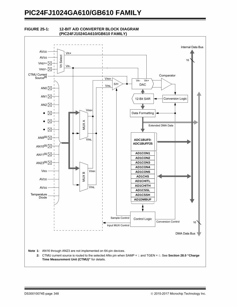
PIC24FJ1024GA610/GB610 FAMILY
FIGURE 25-1: 12-BIT A/D CONVERTER BLOCK DIAGRAM (PIC24FJ1024GA610/GB610 FAMILY)
Comparator
12-Bit SAR
VREF+
DAC
AN9(1)
AN0
AN1
AN2
VREF-
Sample Control
S/H
AVSS
AVDD
ADC1BUF0:ADC1BUFF25
AD1CON1
AD1CON2
AD1CON3
AD1CHS
AD1CHITL
AD1CHITH
Control Logic
Data Formatting
Input MUX ControlConversion Control
Internal Data Bus
16
VR+VR-M
UX
B
VINH
VINL
VINH
VINH
VINL
VINL
VR+
VR-VR
Se
lect
VBG
AD1CSSL
AD1CSSH
Note 1: AN16 through AN23 are not implemented on 64-pin devices.
2: CTMU current source is routed to the selected ANx pin when SAMP = 1 and TGEN = 0. See Section 28.0 “Charge Time Measurement Unit (CTMU)” for details.
Temperature
AVSS
AVDD
AD1CON5
DMA Data Bus
16
AD1CON4
AD1DMBUF
Extended DMA Data
Conversion Logic
MU
X A
AN10(1)
AN11(1)
AN23(1)
Diode
CTMU CurrentSource(2)
DS30010074E-page 348 2015-2017 Microchip Technology Inc.

PIC24FJ1024GA610/GB610 FAMILY
25.2 Extended DMA Operations
In addition to the standard features available on all 12-bitA/D Converters, PIC24FJ1024GA610/GB610 familydevices implement a limited extension of DMA func-tionality. This extension adds features that work withthe device’s DMA Controller to expand the A/Dmodule’s data storage abilities beyond the module’sbuilt-in buffer.
The Extended DMA functionality is controlled by theDMAEN bit (AD1CON1<11>); setting this bit enablesthe functionality. The DMABM bit (AD1CON1<12>)configures how the DMA feature operates.
25.2.1 EXTENDED BUFFER MODE
Extended Buffer mode (DMABM = 1) maps the A/DData Buffer registers and data from all channels above26 into a user-specified area of data RAM. This allowsusers to read the conversion results of channels above26, which do not have their own memory-mapped A/Dbuffer locations, from data memory.
To accomplish this, the DMA must be configured inPeripheral Indirect Addressing mode and the DMAdestination address must point to the beginning of thebuffer. The DMA count must be set to generate aninterrupt after the desired number of conversions.
In Extended Buffer mode, the A/D control bits will functionsimilarly to non-DMA modes. The BUFREGEN bit will stillselect between FIFO mode and Channel-Aligned mode,but the number of words in the destination FIFO will bedetermined by the SMPI<4:0> bits in DMA mode. In FIFOmode, the BUFM bit will still split the output FIFO into twosets of 13 results (the SMPIx bits should be set accord-ingly), and the BUFS bit will still indicate which set ofresults is being written to and which can be read.
25.2.2 PIA MODE
When DMABM = 0, the A/D module is configured tofunction with the DMA Controller for Peripheral IndirectAddressing (PIA) mode operations. In this mode, theA/D module generates an 11-bit Indirect Address (IA).This is ORed with the destination address in the DMAController to define where the A/D conversion data willbe stored.
In PIA mode, the buffer space is created as a series ofcontiguous smaller buffers, one per analog channel.The size of the channel buffer determines how manyanalog channels can be accommodated. The size ofthe buffer is selected by the DMABL<2:0> bits(AD1CON4<2:0>). The size options range from asingle word per buffer to 128 words. Each channel isallocated a buffer of this size, regardless of whether ornot the channel will actually have conversion data.
The IA is created by combining the base address withina channel buffer with three to five bits (depending onthe buffer size) to identify the channel. The baseaddress ranges from zero to seven bits wide, depend-ing on the buffer size. The address is right-padded witha ‘0’ in order to maintain address alignment in the DataSpace. The concatenated channel and base addressbits are then left-padded with zeros, as necessary, tocomplete the 11-bit IA.
The IA is configured to auto-increment which channelis written in each analog input’s sub-buffer during writeoperations by using the SMPIx bits (AD1CON2<6:2>).
As with PIA operations for any DMA-enabled module,the base destination address in the DMADSTn registermust be masked properly to accommodate the IA.Table 25-1 shows how complete addresses areformed. Note that the address masking varies for eachbuffer size option. Because of masking requirements,some address ranges may not be available for certainbuffer sizes. Users should verify that the DMA baseaddress is compatible with the buffer size selected.
Figure 25-2 shows how the parts of the address definethe buffer locations in data memory. In this case, themodule “allocates” 256 bytes of data RAM (1000h to1100h) for 32 buffers of four words each. However, thisis not a hard allocation and nothing prevents theselocations from being used for other purposes. Forexample, in the current case, if Analog Channels 1, 3and 8 are being sampled and converted, conversiondata will only be written to the channel buffers, startingat 1008h, 1018h and 1040h. The holes in the PIA bufferspace can be used for any other purpose. It is theuser’s responsibility to keep track of buffer locationsand prevent data overwrites.
2015-2017 Microchip Technology Inc. DS30010074E-page 349

PIC24FJ1024GA610/GB610 FAMILY
25.3 Registers
The 12-bit A/D Converter is controlled through a total of13 registers:
• AD1CON1 through AD1CON5 (Register 25-1 through Register 25-5)
• AD1CHS (Register 25-6)
• AD1CHITH and AD1CHITL (Register 25-8 and Register 25-9)
• AD1CSSH and AD1CSSL (Register 25-10 and Register 25-11)
• AD1CTMENH and AD1CTMENL (Register 25-12 and Register 25-13)
• AD1DMBUF (not shown) – The 16-bit conversion buffer for Extended Buffer mode
TABLE 25-1: INDIRECT ADDRESS GENERATION IN PIA MODE
DMABL<2:0>Buffer Size per
Channel (words)Generated Offset
Address (lower 11 bits)
Available Input
Channels
Allowable DMADSTn Addresses
000 1 000 00cc ccc0 32 xxxx xxxx xx00 0000
001 2 000 0ccc ccn0 32 xxxx xxxx x000 0000
010 4 000 cccc cnn0 32 xxxx xxxx 0000 0000
011 8 00c cccc nnn0 32 xxxx xxx0 0000 0000
100 16 0cc cccn nnn0 32 xxxx xx00 0000 0000
101 32 ccc ccnn nnn0 32 xxxx x000 0000 0000
110 64 ccc cnnn nnn0 16 xxxx x000 0000 0000
111 128 ccc nnnn nnn0 8 xxxx x000 0000 0000
Legend: ccc = Channel number (three to five bits), n = Base buffer address (zero to seven bits), x = User-definable range of DMADSTn for base address, 0 = Masked bits of DMADSTn for IA
DS30010074E-page 350 2015-2017 Microchip Technology Inc.
PIC24FJ1024GA610/GB610 FAMILY
25.4 Achieving Maximum A/D Converter (ADC) Performance
In order to get the shortest overall conversion time(called the “throughput”) while maintaining accuracy,several factors must be considered. These aredescribed in detail below.
• Dependence of AVDD – If the AVDD supply is < 2.7V, the Charge Pump Enable bit (PUMPEN, AD1CON3<13>) should be set to ‘1’. The input channel multiplexer has a varying resistance with AVDD (the lower AVDD, the higher the internal switch resistance). The charge pump provides a higher internal AVDD to keep the switch resistance as low as possible.
• Dependence on TAD – The ADC timing is driven by TAD, not TCYC. Selecting the TAD time correctly is critical to getting the best ADC throughput. It is important to note that the overall ADC throughput is not simply the ‘Conversion Time’ of the SAR; it is the combination of the Conversion Time, the Sample Time and additional TAD delays for internal synchronization logic.
• Relationship between TCYC and TAD – There is not a fixed 1:1 timing relationship between TCYC and TAD. The fastest possible throughput is funda-mentally set by TAD (min), not by TCYC. The TAD time is set as a programmable integer multiple of TCYC by the ADCS<7:0> bits. Referring to Table 33-26, the TAD (min) time is greater than the 4 MHz period of the dedicated ADC RC clock generator. Therefore, TAD must be 2 TCYC in order to use the RC clock for fastest throughput. The TAD (min) is a multiple of 3.597 MHz as opposed to 4 MHz. To run as fast as possible, TCYC must be a multiple of TAD (min) because values of ADCSx are integers. For example, if a standard “color burst” crystal of 14.31818 MHz is used, TCYC is 279.4 ns, which is very close to TAD (min) and the ADC throughput is optimal. Running at 16 MHz will actually reduce the throughput, because TAD will have to be 500 ns as the TCYC of 250 ns violates TAD (min).
• Dependence on driving Source Resistance (RS) – Certain transducers have high output impedance (> 2.5 kΩ). Having a high RS will require longer sampling time to charge the S/H capacitor through the resistance path (see Figure 25-3). The worst case scenario is a full-range voltage step of AVSS to AVDD, with the sampling cap at AVSS. The capacitor time constant is (RS + RIC + RSS) (CHOLD) and the sample time needs to be 6 time constants minimum (8 preferred). Since the ADC logic timing is TAD-based, the sample time (in TAD) must be long enough, over all conditions, to charge/discharge CHOLD. Do not assume one TAD is sufficient sample time; longer times may be required to achieve the accuracy needed by the application. The value of CHOLD is 40 pF.
A small amount of charge is present at the ADC inputpin when the sample switch is closed. If RS is high, thiswill generate a DC error exceeding 1 LSB. KeepingRS < 50Ω is recommenced for best results. The errorcan also be reduced by increasing sample time (a 2 kΩvalue of RS requires a 3 µS sample time to eliminatethe error).
• Calculating Throughput – The throughput of the ADC is based on TAD. The throughput is given by:
where:
Sample Time is the calculated TAD periods for theapplication.
SAR Conversion Time is 12 TAD for 10-bit and 14 TAD for12-bit conversions.
Clock Sync Time is 2.5 TAD (worst case scenario).
For example, using an 8 MHz FRC means theTCYC = 250 ns. This requires: TAD = 2 TCYC = 500 ns.Therefore, the throughput is:
Note that the clock sync delay could be as little as1.5 TAD, which could produce 121 KS/sec, but thatcannot be ensured as the timing relationship isasynchronous and not specified. The worst case timingof 2.5 TAD should be used to calculate throughput.
For example, if a certain transducer has a 20 kΩ outputimpedance, the maximum sample time is determinedby:
If TAD = 500 ns, this requires a Sample Time of 4.95 us/500 ns = 10 TAD (for a full-step voltage on thetransducer output).
Throughput =1
Sample Time + SAR Conversion Time + Clock Sync Time)(
Throughput =1
500 ns + 14 • 500 ns + 2.5 • 500 ns)( = 114.28 KS/sec
Sample Time = 6 • (RS + RIC + RSS) • CHOLD
= 6 • (20K + 250 + 350) • 40 pF
= 4.95 µS
2015-2017 Microchip Technology Inc. DS30010074E-page 351

PIC24FJ1024GA610/GB610 FAMILY
FIGURE 25-2: EXAMPLE OF BUFFER ADDRESS GENERATION IN PIA MODE (4-WORD BUFFERS PER CHANNEL)
Data RAM
Destination
A/D Module(PIA Mode)
BBA
DMA Channel
DMADSTn
nn (0-3)
1000h (DMA Base Address)
Range
Channel
ccccc (0-31) 000 cccc cnn0 (IA)
1000h
DMABL<2:0> = 010(4 Words Per Input)
1008h1010h1018h
10F8h
1100h
Ch 0 Buffer (4 Words)Ch 1 Buffer (4 Words)Ch 2 Buffer (4 Words)Ch 3 Buffer (4 Words)
Ch 29 Buffer (4 Words)Ch 29 Buffer (4 Words)Ch 31 Buffer (4 Words)
10F0h
(Buffer Base Address)
1000h1002h1004h1006h
Ch 0, Word 0Ch 0, Word 1Ch 0, Word 2Ch 0, Word 3Ch 1, Word 0Ch 1, Word 1Ch 1, Word 2Ch 1, Word 3
1008h100Ah100Ch100Eh
0001 0000 0000 00000001 0000 0000 00100001 0000 0000 01000001 0000 0000 01100001 0000 0000 10000001 0000 0000 10100001 0000 0000 11000001 0000 0000 1110
DMA Base AddressAddress Mask
Channel AddressBuffer Address
1038h1040h
Ch 7 Buffer (4 Words)Ch 8 Buffer (4 Words)
DS30010074E-page 352 2015-2017 Microchip Technology Inc.

PIC24FJ1024GA610/GB610 FAMILY
REGISTER 25-1: AD1CON1: A/D CONTROL REGISTER 1
R/W-0 U-0 R/W-0 R/W-0 R/W-0 R/W-0 R/W-0 R/W-0
ADON — ADSIDL DMABM(1) DMAEN MODE12 FORM1 FORM0
bit 15 bit 8
R/W-0 R/W-0 R/W-0 R/W-0 U-0 R/W-0 R/W-0, HSC R/C-0, HSC
SSRC3 SSRC2 SSRC1 SSRC0 — ASAM SAMP DONE
bit 7 bit 0
Legend: C = Clearable bit U = Unimplemented bit, read as ‘0’
R = Readable bit W = Writable bit HSC = Hardware Settable/Clearable bit
-n = Value at POR ‘1’ = Bit is set ‘0’ = Bit is cleared x = Bit is unknown
bit 15 ADON: A/D Operating Mode bit
1 = A/D Converter is operating0 = A/D Converter is off
bit 14 Unimplemented: Read as ‘0’
bit 13 ADSIDL: A/D Stop in Idle Mode bit
1 = Discontinues module operation when device enters Idle mode0 = Continues module operation in Idle mode
bit 12 DMABM: Extended DMA Buffer Mode Select bit(1)
1 = Extended Buffer mode: Buffer address is defined by the DMADSTn register0 = PIA mode: Buffer addresses are defined by the DMA Controller and AD1CON4<2:0>
bit 11 DMAEN: Extended DMA/Buffer Enable bit
1 = Extended DMA and buffer features are enabled0 = Extended features are disabled
bit 10 MODE12: A/D 12-Bit Operation Mode bit
1 = 12-bit A/D operation0 = 10-bit A/D operation
bit 9-8 FORM<1:0>: Data Output Format bits (see formats following)
11 = Fractional result, signed, left justified10 = Absolute fractional result, unsigned, left justified01 = Decimal result, signed, right justified00 = Absolute decimal result, unsigned, right justified
bit 7-4 SSRC<3:0>: Sample Clock Source Select bits
0000 = SAMP is cleared by software0001 = INT00010 = Timer30100 = CTMU Trigger0101 = Timer1 (will not trigger during Sleep mode)0110 = Timer1 (may trigger during Sleep mode)0111 = Auto-Convert mode
bit 3 Unimplemented: Read as ‘0’
bit 2 ASAM: A/D Sample Auto-Start bit
1 = Sampling begins immediately after last conversion; SAMP bit is auto-set0 = Sampling begins when SAMP bit is manually set
Note 1: This bit is only available when Extended DMA and buffer features are available (DMAEN = 1).
2015-2017 Microchip Technology Inc. DS30010074E-page 353

PIC24FJ1024GA610/GB610 FAMILY
bit 1 SAMP: A/D Sample Enable bit
1 = A/D Sample-and-Hold amplifiers are sampling0 = A/D Sample-and-Hold amplifiers are holding
bit 0 DONE: A/D Conversion Status bit
1 = A/D conversion cycle has completed 0 = A/D conversion cycle has not started or is in progress
REGISTER 25-1: AD1CON1: A/D CONTROL REGISTER 1 (CONTINUED)
Note 1: This bit is only available when Extended DMA and buffer features are available (DMAEN = 1).
DS30010074E-page 354 2015-2017 Microchip Technology Inc.

PIC24FJ1024GA610/GB610 FAMILY
REGISTER 25-2: AD1CON2: A/D CONTROL REGISTER 2
R/W-0 R/W-0 R/W-0 r-0 R/W-0 R/W-0 U-0 U-0
PVCFG1 PVCFG0 NVCFG0 — BUFREGEN CSCNA — —
bit 15 bit 8
R-0 R/W-0 R/W-0 R/W-0 R/W-0 R/W-0 R/W-0 R/W-0
BUFS SMPI4 SMPI3 SMPI2 SMPI1 SMPI0 BUFM ALTS
bit 7 bit 0
Legend: r = Reserved bit
R = Readable bit W = Writable bit U = Unimplemented bit, read as ‘0’
-n = Value at POR ‘1’ = Bit is set ‘0’ = Bit is cleared x = Bit is unknown
bit 15-14 PVCFG<1:0>: A/D Converter Positive Voltage Reference Configuration bits
1x = Unimplemented, do not use01 = External VREF+00 = AVDD
bit 13 NVCFG0: A/D Converter Negative Voltage Reference Configuration bit
1 = External VREF-0 = AVSS
bit 12 Reserved: Maintain as ‘0’
bit 11 BUFREGEN: A/D Buffer Register Enable bit
1 = Conversion result is loaded into the buffer location determined by the converted channel0 = A/D result buffer is treated as a FIFO
bit 10 CSCNA: Scan Input Selections for CH0+ During Sample A bit
1 = Scans inputs0 = Does not scan inputs
bit 9-8 Unimplemented: Read as ‘0’
bit 7 BUFS: Buffer Fill Status bit
When DMAEN = 1 and DMABM = 1:1 = A/D is currently filling the destination buffer from [buffer start + (buffer size/2)] to
[buffer start + (buffer size – 1)]. User should access data located from [buffer start] to [buffer start + (buffer size/2) – 1].
0 = A/D is currently filling the destination buffer from [buffer start] to [buffer start + (buffer size/2) – 1].User should access data located from [buffer start + (buffer size/2)] to [buffer start + (buffer size – 1)].
When DMAEN = 0:1 = A/D is currently filling ADC1BUF13-ADC1BUF25, user should access data in
ADC1BUF0-ADC1BUF120 = A/D is currently filling ADC1BUF0-ADC1BUF12, user should access data in
ADC1BUF13-ADC1BUF25
2015-2017 Microchip Technology Inc. DS30010074E-page 355
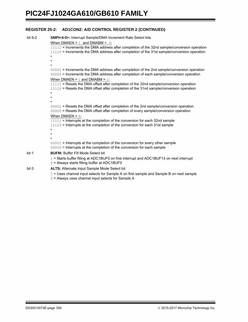
PIC24FJ1024GA610/GB610 FAMILY
bit 6-2 SMPI<4:0>: Interrupt Sample/DMA Increment Rate Select bits
When DMAEN = 1 and DMABM = 0:11111 = Increments the DMA address after completion of the 32nd sample/conversion operation11110 = Increments the DMA address after completion of the 31st sample/conversion operation•••00001 = Increments the DMA address after completion of the 2nd sample/conversion operation00000 = Increments the DMA address after completion of each sample/conversion operation
When DMAEN = 1 and DMABM = 1:11111 = Resets the DMA offset after completion of the 32nd sample/conversion operation11110 = Resets the DMA offset after completion of the 31nd sample/conversion operation•••00001 = Resets the DMA offset after completion of the 2nd sample/conversion operation00000 = Resets the DMA offset after completion of every sample/conversion operation
When DMAEN = 0:11111 = Interrupts at the completion of the conversion for each 32nd sample11110 = Interrupts at the completion of the conversion for each 31st sample•••00001 = Interrupts at the completion of the conversion for every other sample00000 = Interrupts at the completion of the conversion for each sample
bit 1 BUFM: Buffer Fill Mode Select bit
1 = Starts buffer filling at ADC1BUF0 on first interrupt and ADC1BUF13 on next interrupt0 = Always starts filling buffer at ADC1BUF0
bit 0 ALTS: Alternate Input Sample Mode Select bit
1 = Uses channel input selects for Sample A on first sample and Sample B on next sample0 = Always uses channel input selects for Sample A
REGISTER 25-2: AD1CON2: A/D CONTROL REGISTER 2 (CONTINUED)
DS30010074E-page 356 2015-2017 Microchip Technology Inc.
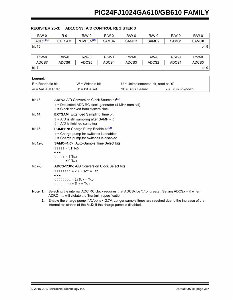
PIC24FJ1024GA610/GB610 FAMILY
REGISTER 25-3: AD1CON3: A/D CONTROL REGISTER 3
R/W-0 R-0 R/W-0 R/W-0 R/W-0 R/W-0 R/W-0 R/W-0
ADRC(1) EXTSAM PUMPEN(2) SAMC4 SAMC3 SAMC2 SAMC1 SAMC0
bit 15 bit 8
R/W-0 R/W-0 R/W-0 R/W-0 R/W-0 R/W-0 R/W-0 R/W-0
ADCS7 ADCS6 ADCS5 ADCS4 ADCS3 ADCS2 ADCS1 ADCS0
bit 7 bit 0
Legend:
R = Readable bit W = Writable bit U = Unimplemented bit, read as ‘0’
-n = Value at POR ‘1’ = Bit is set ‘0’ = Bit is cleared x = Bit is unknown
bit 15 ADRC: A/D Conversion Clock Source bit(1)
1 = Dedicated ADC RC clock generator (4 MHz nominal)0 = Clock derived from system clock
bit 14 EXTSAM: Extended Sampling Time bit
1 = A/D is still sampling after SAMP = 00 = A/D is finished sampling
bit 13 PUMPEN: Charge Pump Enable bit(2)
1 = Charge pump for switches is enabled0 = Charge pump for switches is disabled
bit 12-8 SAMC<4:0>: Auto-Sample Time Select bits
11111 = 31 TAD
00001 = 1 TAD
00000 = 0 TAD
bit 7-0 ADCS<7:0>: A/D Conversion Clock Select bits
11111111 = 256 • TCY = TAD
00000001 = 2•TCY = TAD
00000000 = TCY = TAD
Note 1: Selecting the internal ADC RC clock requires that ADCSx be ‘1’ or greater. Setting ADCSx = 0 when ADRC = 1 will violate the TAD (min) specification.
2: Enable the charge pump if AVDD is < 2.7V. Longer sample times are required due to the increase of the internal resistance of the MUX if the charge pump is disabled.
2015-2017 Microchip Technology Inc. DS30010074E-page 357

PIC24FJ1024GA610/GB610 FAMILY
REGISTER 25-4: AD1CON4: A/D CONTROL REGISTER 4
U-0 U-0 U-0 U-0 U-0 U-0 U-0 U-0
— — — — — — — —
bit 15 bit 8
U-0 U-0 U-0 U-0 U-0 R/W-0 R/W-0 R/W-0
— — — — — DMABL<2:0>(1)
bit 7 bit 0
Legend:
R = Readable bit W = Writable bit U = Unimplemented bit, read as ‘0’
-n = Value at POR ‘1’ = Bit is set ‘0’ = Bit is cleared x = Bit is unknown
bit 15-3 Unimplemented: Read as ‘0’
bit 2-0 DMABL<2:0>: DMA Buffer Size Select bits(1)
111 = Allocates 128 words of buffer to each analog input110 = Allocates 64 words of buffer to each analog input101 = Allocates 32 words of buffer to each analog input100 = Allocates 16 words of buffer to each analog input011 = Allocates 8 words of buffer to each analog input010 = Allocates 4 words of buffer to each analog input001 = Allocates 2 words of buffer to each analog input000 = Allocates 1 word of buffer to each analog input
Note 1: The DMABL<2:0> bits are only used when AD1CON1<11> = 1 and AD1CON1<12> = 0; otherwise, their value is ignored.
DS30010074E-page 358 2015-2017 Microchip Technology Inc.
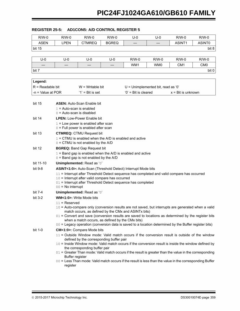
PIC24FJ1024GA610/GB610 FAMILY
REGISTER 25-5: AD1CON5: A/D CONTROL REGISTER 5
R/W-0 R/W-0 R/W-0 R/W-0 U-0 U-0 R/W-0 R/W-0
ASEN LPEN CTMREQ BGREQ — — ASINT1 ASINT0
bit 15 bit 8
U-0 U-0 U-0 U-0 R/W-0 R/W-0 R/W-0 R/W-0
— — — — WM1 WM0 CM1 CM0
bit 7 bit 0
Legend:
R = Readable bit W = Writable bit U = Unimplemented bit, read as ‘0’
-n = Value at POR ‘1’ = Bit is set ‘0’ = Bit is cleared x = Bit is unknown
bit 15 ASEN: Auto-Scan Enable bit
1 = Auto-scan is enabled0 = Auto-scan is disabled
bit 14 LPEN: Low-Power Enable bit
1 = Low power is enabled after scan0 = Full power is enabled after scan
bit 13 CTMREQ: CTMU Request bit
1 = CTMU is enabled when the A/D is enabled and active0 = CTMU is not enabled by the A/D
bit 12 BGREQ: Band Gap Request bit
1 = Band gap is enabled when the A/D is enabled and active0 = Band gap is not enabled by the A/D
bit 11-10 Unimplemented: Read as ‘0’
bit 9-8 ASINT<1:0>: Auto-Scan (Threshold Detect) Interrupt Mode bits
11 = Interrupt after Threshold Detect sequence has completed and valid compare has occurred10 = Interrupt after valid compare has occurred01 = Interrupt after Threshold Detect sequence has completed00 = No interrupt
bit 7-4 Unimplemented: Read as ‘0’
bit 3-2 WM<1:0>: Write Mode bits
11 = Reserved10 = Auto-compare only (conversion results are not saved, but interrupts are generated when a valid
match occurs, as defined by the CMx and ASINTx bits)01 = Convert and save (conversion results are saved to locations as determined by the register bits
when a match occurs, as defined by the CMx bits)00 = Legacy operation (conversion data is saved to a location determined by the Buffer register bits)
bit 1-0 CM<1:0>: Compare Mode bits
11 = Outside Window mode: Valid match occurs if the conversion result is outside of the windowdefined by the corresponding buffer pair
10 = Inside Window mode: Valid match occurs if the conversion result is inside the window defined bythe corresponding buffer pair
01 = Greater Than mode: Valid match occurs if the result is greater than the value in the correspondingBuffer register
00 = Less Than mode: Valid match occurs if the result is less than the value in the corresponding Bufferregister
2015-2017 Microchip Technology Inc. DS30010074E-page 359
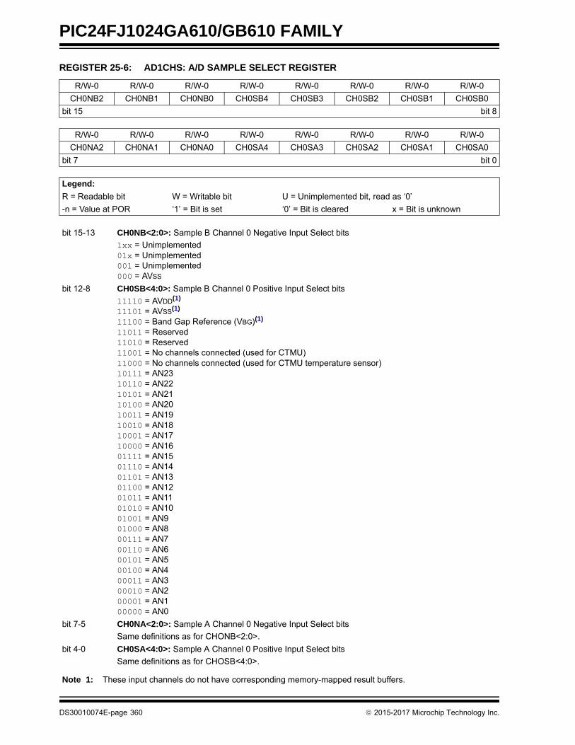
PIC24FJ1024GA610/GB610 FAMILY
REGISTER 25-6: AD1CHS: A/D SAMPLE SELECT REGISTER
R/W-0 R/W-0 R/W-0 R/W-0 R/W-0 R/W-0 R/W-0 R/W-0
CH0NB2 CH0NB1 CH0NB0 CH0SB4 CH0SB3 CH0SB2 CH0SB1 CH0SB0
bit 15 bit 8
R/W-0 R/W-0 R/W-0 R/W-0 R/W-0 R/W-0 R/W-0 R/W-0
CH0NA2 CH0NA1 CH0NA0 CH0SA4 CH0SA3 CH0SA2 CH0SA1 CH0SA0
bit 7 bit 0
Legend:
R = Readable bit W = Writable bit U = Unimplemented bit, read as ‘0’
-n = Value at POR ‘1’ = Bit is set ‘0’ = Bit is cleared x = Bit is unknown
bit 15-13 CH0NB<2:0>: Sample B Channel 0 Negative Input Select bits
1xx = Unimplemented01x = Unimplemented001 = Unimplemented000 = AVSS
bit 12-8 CH0SB<4:0>: Sample B Channel 0 Positive Input Select bits
11110 = AVDD(1)
11101 = AVSS(1)
11100 = Band Gap Reference (VBG)(1)
11011 = Reserved11010 = Reserved11001 = No channels connected (used for CTMU)11000 = No channels connected (used for CTMU temperature sensor)10111 = AN2310110 = AN2210101 = AN2110100 = AN2010011 = AN1910010 = AN1810001 = AN1710000 = AN1601111 = AN1501110 = AN1401101 = AN1301100 = AN1201011 = AN1101010 = AN1001001 = AN901000 = AN800111 = AN700110 = AN600101 = AN500100 = AN400011 = AN300010 = AN200001 = AN100000 = AN0
bit 7-5 CH0NA<2:0>: Sample A Channel 0 Negative Input Select bits
Same definitions as for CHONB<2:0>.
bit 4-0 CH0SA<4:0>: Sample A Channel 0 Positive Input Select bits
Same definitions as for CHOSB<4:0>.
Note 1: These input channels do not have corresponding memory-mapped result buffers.
DS30010074E-page 360 2015-2017 Microchip Technology Inc.
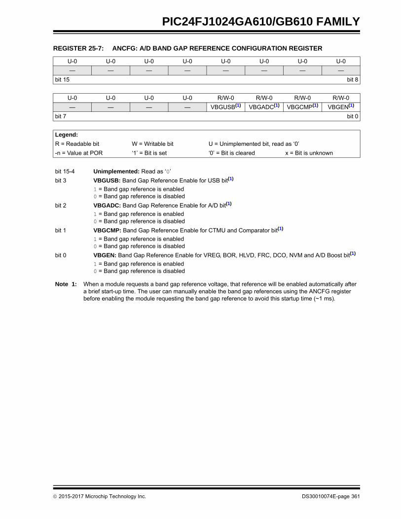
PIC24FJ1024GA610/GB610 FAMILY
REGISTER 25-7: ANCFG: A/D BAND GAP REFERENCE CONFIGURATION REGISTER
U-0 U-0 U-0 U-0 U-0 U-0 U-0 U-0
— — — — — — — —
bit 15 bit 8
U-0 U-0 U-0 U-0 R/W-0 R/W-0 R/W-0 R/W-0
— — — — VBGUSB(1) VBGADC(1) VBGCMP(1) VBGEN(1)
bit 7 bit 0
Legend:
R = Readable bit W = Writable bit U = Unimplemented bit, read as ‘0’
-n = Value at POR ‘1’ = Bit is set ‘0’ = Bit is cleared x = Bit is unknown
bit 15-4 Unimplemented: Read as ‘0’
bit 3 VBGUSB: Band Gap Reference Enable for USB bit(1)
1 = Band gap reference is enabled0 = Band gap reference is disabled
bit 2 VBGADC: Band Gap Reference Enable for A/D bit(1)
1 = Band gap reference is enabled0 = Band gap reference is disabled
bit 1 VBGCMP: Band Gap Reference Enable for CTMU and Comparator bit(1)
1 = Band gap reference is enabled0 = Band gap reference is disabled
bit 0 VBGEN: Band Gap Reference Enable for VREG, BOR, HLVD, FRC, DCO, NVM and A/D Boost bit(1)
1 = Band gap reference is enabled0 = Band gap reference is disabled
Note 1: When a module requests a band gap reference voltage, that reference will be enabled automatically after a brief start-up time. The user can manually enable the band gap references using the ANCFG register before enabling the module requesting the band gap reference to avoid this startup time (~1 ms).
2015-2017 Microchip Technology Inc. DS30010074E-page 361

PIC24FJ1024GA610/GB610 FAMILY
REGISTER 25-8: AD1CHITH: A/D SCAN COMPARE HIT REGISTER (HIGH WORD)(1)
U-0 U-0 U-0 U-0 U-0 U-0 R/W-0 R/W-0
— — — — — — CHH<25:24>
bit 15 bit 8
R/W-0 R/W-0 R/W-0 R/W-0 R/W-0 R/W-0 R/W-0 R/W-0
CHH<23:16>
bit 7 bit 0
Legend:
R = Readable bit W = Writable bit U = Unimplemented bit, read as ‘0’
-n = Value at POR ‘1’ = Bit is set ‘0’ = Bit is cleared x = Bit is unknown
bit 15-10 Unimplemented: Read as ‘0’
bit 9-0 CHH<25:16>: A/D Compare Hit bits
If CM<1:0> = 11:1 = A/D Result Buffer n has been written with data or a match has occurred0 = A/D Result Buffer n has not been written with data
For All Other Values of CM<1:0>:1 = A match has occurred on A/D Result Channel n0 = No match has occurred on A/D Result Channel n
Note 1: AD1CHITH is not available on 64-pin parts.
REGISTER 25-9: AD1CHITL: A/D SCAN COMPARE HIT REGISTER (LOW WORD)(1)
R/W-0 R/W-0 R/W-0 R/W-0 R/W-0 R/W-0 R/W-0 R/W-0
CHH<15:8>
bit 15 bit 8
R/W-0 R/W-0 R/W-0 R/W-0 R/W-0 R/W-0 R/W-0 R/W-0
CHH<7:0>
bit 7 bit 0
Legend:
R = Readable bit W = Writable bit U = Unimplemented bit, read as ‘0’
-n = Value at POR ‘1’ = Bit is set ‘0’ = Bit is cleared x = Bit is unknown
bit 15-0 CHH<15:0>: A/D Compare Hit bits
If CM<1:0> = 11:1 = A/D Result Buffer n has been written with data or a match has occurred0 = A/D Result Buffer n has not been written with data
For All Other Values of CM<1:0>:1 = A match has occurred on A/D Result Channel n0 = No match has occurred on A/D Result Channel n
Note 1: AD1CHITL is not available on 64-pin parts.
DS30010074E-page 362 2015-2017 Microchip Technology Inc.

PIC24FJ1024GA610/GB610 FAMILY
REGISTER 25-10: AD1CSSH: A/D INPUT SCAN SELECT REGISTER (HIGH WORD)
U-0 R/W-0 R/W-0 R/W-0 U-0 R/W-0 R/W-0 R/W-0
— CSS<30:28> — CSS<26:24>
bit 15 bit 8
R/W-0 R/W-0 R/W-0 R/W-0 R/W-0 R/W-0 R/W-0 R/W-0
CSS<23:16>
bit 7 bit 0
Legend:
R = Readable bit W = Writable bit U = Unimplemented bit, read as ‘0’
-n = Value at POR ‘1’ = Bit is set ‘0’ = Bit is cleared x = Bit is unknown
bit 15 Unimplemented: Read as ‘0’
bit 14-12 CSS<30:28>: A/D Input Scan Selection bits
1 = Includes corresponding channel for input scan0 = Skips channel for input scan
bit 11 Unimplemented: Read as ‘0’
bit 10-0 CSS<26:16>: A/D Input Scan Selection bits
1 = Includes corresponding channel for input scan0 = Skips channel for input scan
REGISTER 25-11: AD1CSSL: A/D INPUT SCAN SELECT REGISTER (LOW WORD)
R/W-0 R/W-0 R/W-0 R/W-0 R/W-0 R/W-0 R/W-0 R/W-0
CSS<15:8>
bit 15 bit 8
R/W-0 R/W-0 R/W-0 R/W-0 R/W-0 R/W-0 R/W-0 R/W-0
CSS<7:0>
bit 7 bit 0
Legend:
R = Readable bit W = Writable bit U = Unimplemented bit, read as ‘0’
-n = Value at POR ‘1’ = Bit is set ‘0’ = Bit is cleared x = Bit is unknown
bit 15-0 CSS<15:0>: A/D Input Scan Selection bits
1 = Includes corresponding channel for input scan0 = Skips channel for input scan
2015-2017 Microchip Technology Inc. DS30010074E-page 363

PIC24FJ1024GA610/GB610 FAMILY
REGISTER 25-12: AD1CTMENH: A/D CTMU ENABLE REGISTER (HIGH WORD)
U-0 R/W-0 R/W-0 R/W-0 U-0 U-0 R/W-0 R/W-0
— CTMEN<30:28> — — CTMEN<25:24>
bit 15 bit 8
R/W-0 R/W-0 R/W-0 R/W-0 R/W-0 R/W-0 R/W-0 R/W-0
CTMEN<23:16>(1)
bit 7 bit 0
Legend:
R = Readable bit W = Writable bit U = Unimplemented bit, read as ‘0’
-n = Value at POR ‘1’ = Bit is set ‘0’ = Bit is cleared x = Bit is unknown
bit 15 Unimplemented: Read as ‘0’
bit 14-12 CTMEN<30:28>: CTMU Enabled During Conversion bits
1 = CTMU is enabled and connected to the selected channel during conversion0 = CTMU is not connected to this channel
bit 11-10 Unimplemented: Read as ‘0’
bit 9-0 CTMEN<25:16>: CTMU Enabled During Conversion bits(1)
1 = CTMU is enabled and connected to the selected channel during conversion0 = CTMU is not connected to this channel
Note 1: CTMEN<23:16> bits are not available on 64-pin parts.
REGISTER 25-13: AD1CTMENL: A/D CTMU ENABLE REGISTER (LOW WORD)
R/W-0 R/W-0 R/W-0 R/W-0 R/W-0 R/W-0 R/W-0 R/W-0
CTMEN<15:8>
bit 15 bit 8
R/W-0 R/W-0 R/W-0 R/W-0 R/W-0 R/W-0 R/W-0 R/W-0
CTMEN<7:0>
bit 7 bit 0
Legend:
R = Readable bit W = Writable bit U = Unimplemented bit, read as ‘0’
-n = Value at POR ‘1’ = Bit is set ‘0’ = Bit is cleared x = Bit is unknown
bit 15-0 CTMEN<15:0>: CTMU Enabled During Conversion bits
1 = CTMU is enabled and connected to the selected channel during conversion0 = CTMU is not connected to this channel
DS30010074E-page 364 2015-2017 Microchip Technology Inc.

PIC24FJ1024GA610/GB610 FAMILY
FIGURE 25-3: 12-BIT A/D CONVERTER ANALOG INPUT MODEL
EQUATION 25-1: A/D CONVERSION CLOCK PERIOD
CPINVA
Rs ANx
ILEAKAGE
RIC 250
SamplingSwitch
RSS
CHOLD
AVSS
= 40 pF500 nA
Legend: CPIN
VT
ILEAKAGE
RIC
RSS
CHOLD
= Input Capacitance= Threshold Voltage= Leakage Current at the pin due to
= Interconnect Resistance= Sampling Switch Resistance= Sample/Hold Capacitance
Various Junctions
Note: The CPIN value depends on the device package and is not tested. The effect of CPIN is negligible if Rs 2.5 k.
(RSS 3 k)
AVDD
VT = 0.6V
VT = 0.6V
SS–S/H+
= S/H Input Capacitance
SamplingSwitch
RMIN
RMAX
AVDDMINAVDD (V)
AVDDMAX
TAD = TCY (ADCS + 1)
ADCS = – 1TAD
TCY
Note: Based on TCY = 2/FOSC; Doze mode and PLL are disabled.
2015-2017 Microchip Technology Inc. DS30010074E-page 365

PIC24FJ1024GA610/GB610 FAMILY
FIGURE 25-4: 12-BIT A/D TRANSFER FUNCTION
0010 0000 0001 (2049)
0010 0000 0010 (2050)
0010 0000 0011 (2051)
0001 1111 1101 (2045)
0001 1111 1110 (2046)
0001 1111 1111 (2047)
1111 1111 1110 (4094)
1111 1111 1111 (4095)
0000 0000 0000 (0)
0000 0000 0001 (1)
Output Code
0010 0000 0000 (2048)
(VIN
H –
VIN
L)
VR
-
VR
+ –
VR
-
4096
204
8 *
(V
R+
– V
R-)
409
6
VR
+
VR
- +
VR
-+
409
5 *
(V
R+
– V
R-)
409
6V
R- +
0
(Binary (Decimal))
Voltage Level
DS30010074E-page 366 2015-2017 Microchip Technology Inc.
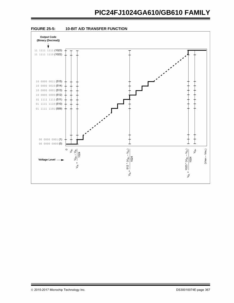
PIC24FJ1024GA610/GB610 FAMILY
FIGURE 25-5: 10-BIT A/D TRANSFER FUNCTION
10 0000 0001 (513)
10 0000 0010 (514)
10 0000 0011 (515)
01 1111 1101 (509)
01 1111 1110 (510)
01 1111 1111 (511)
11 1111 1110 (1022)
11 1111 1111 (1023)
00 0000 0000 (0)
00 0000 0001 (1)
Output Code
10 0000 0000 (512)
(VIN
H –
VIN
L)
VR
-
VR
+ –
VR
-
102
4
512
* (
VR
+ –
VR
-)
102
4
VR
+
VR
- +
VR
-+
1023
* (
VR
+ –
VR
-)
102
4V
R- +
0
(Binary (Decimal))
Voltage Level
2015-2017 Microchip Technology Inc. DS30010074E-page 367

PIC24FJ1024GA610/GB610 FAMILY
NOTES:
DS30010074E-page 368 2015-2017 Microchip Technology Inc.

PIC24FJ1024GA610/GB610 FAMILY
26.0 TRIPLE COMPARATOR MODULE
The triple comparator module provides three dual inputcomparators. The inputs to the comparator can beconfigured to use any one of five external analog inputs(CxINA, CxINB, CxINC, CxIND and CVREF+) and a
voltage reference input from one of the internal bandgap references or the comparator voltage referencegenerator (VBG and CVREF).
The comparator outputs may be directly connected tothe CxOUT pins. When the respective COE bit equals‘1’, the I/O pad logic makes the unsynchronized outputof the comparator available on the pin.
A simplified block diagram of the module in shown inFigure 26-1. Diagrams of the possible individualcomparator configurations are shown in Figure 26-2through Figure 26-4.
Each comparator has its own control register,CMxCON (Register 26-1), for enabling and configuringits operation. The output and event status of all threecomparators is provided in the CMSTAT register(Register 26-2).
FIGURE 26-1: TRIPLE COMPARATOR MODULE BLOCK DIAGRAM
Note: This data sheet summarizes the features ofthis group of PIC24F devices. It is notintended to be a comprehensive referencesource. For more information, refer to the“dsPIC33/PIC24 Family Reference Man-ual”, “Scalable Comparator Module”(DS39734), which is available from theMicrochip web site (www.microchip.com).The information in this data sheetsupersedes the information in the FRM.
C1
VIN-
VIN+CxINB
CxINC
CxINA
CxIND
CVREF+
VBG
C2
VIN-
VIN+
C3
VIN-
VIN+
COE
C1OUTPin
CPOL
Trigger/InterruptLogic
CEVT
EVPOL<1:0>
COUT
InputSelectLogic
CCH<1:0>
CREF
COE
C2OUTPin
CPOL
Trigger/InterruptLogic
CEVT
EVPOL<1:0>
COUT
COE
C3OUTPin
CPOL
Trigger/InterruptLogic
CEVT
EVPOL<1:0>
COUT
CVREF+
–
CVREFM<1:0>(1)
CVREFP(1)
+
01
00
10
1100
11
1
0
0
1
Note 1: Refer to the CVRCON register (Register 27-1) for bit details.
Comparator VoltageReference
2015-2017 Microchip Technology Inc. DS30010074E-page 369

PIC24FJ1024GA610/GB610 FAMILY
FIGURE 26-2: INDIVIDUAL COMPARATOR CONFIGURATIONS WHEN CREF = 0
FIGURE 26-3: INDIVIDUAL COMPARATOR CONFIGURATIONS WHEN CREF = 1 AND CVREFP = 0
Cx
VIN-
VIN+Off (Read as ‘0’)
Comparator OffCEN = 0, CREF = x, CCH<1:0> = xx
Comparator CxINB > CxINA Compare CEN = 1, CCH<1:0> = 00, CVREFM<1:0> = xx
COE
CxOUT
Cx
VIN-
VIN+
COE
CxINB
CxINA
Comparator CxIND > CxINA Compare CEN = 1, CCH<1:0> = 10, CVREFM<1:0> = xx
Cx
VIN-
VIN+
COE
CxOUT
CxIND
CxINA
Comparator CxINC > CxINA Compare
Cx
VIN-
VIN+
COE
CxINC
CxINA
Comparator VBG > CxINA Compare
Cx
VIN-
VIN+
COE
VBG
CxINA
Pin
Pin
CxOUTPin
CxOUTPin
CxOUTPin
Comparator CVREF+ > CxINA Compare
Cx
VIN-
VIN+
COE
CxOUT
CVREF+
CxINA
Pin
CEN = 1, CCH<1:0> = 11, CVREFM<1:0> = 11
CEN = 1, CCH<1:0> = 01, CVREFM<1:0> = xx
CEN = 1, CCH<1:0> = 11, CVREFM<1:0> = 00
Comparator CxIND > CVREF Compare
Cx
VIN-
VIN+
COE
CxIND
CVREF CxOUTPin
Comparator VBG > CVREF Compare
Cx
VIN-
VIN+
COE
VBG
CVREF CxOUTPin
Comparator CxINC > CVREF Compare
Cx
VIN-
VIN+
COE
CxINC
CVREF CxOUTPin
Comparator CxINB > CVREF Compare CEN = 1, CCH<1:0> = 00, CVREFM<1:0> = xx
Cx
VIN-
VIN+
COE
CxINB
CVREF CxOUTPin
Comparator CVREF+ > CVREF Compare
Cx
VIN-
VIN+
COE
CVREF+
CVREF CxOUTPin
CEN = 1, CCH<1:0> = 10, CVREFM<1:0> = xx
CEN = 1, CCH<1:0> = 11, CVREFM<1:0> = 11
CEN = 1, CCH<1:0> = 11, CVREFM<1:0> = 00
CEN = 1, CCH<1:0> = 01, CVREFM<1:0> = xx
DS30010074E-page 370 2015-2017 Microchip Technology Inc.

PIC24FJ1024GA610/GB610 FAMILY
FIGURE 26-4: INDIVIDUAL COMPARATOR CONFIGURATIONS WHEN CREF = 1 AND CVREFP = 1
Comparator CxIND > CVREF Compare
Cx
VIN-
VIN+
COE
CxIND
CVREF+ CxOUTPin
Comparator VBG > CVREF Compare
Cx
VIN-
VIN+
COE
VBG
CVREF+ CxOUTPin
Comparator CxINC > CVREF Compare
Cx
VIN-
VIN+
COE
CxINC
CVREF+ CxOUTPin
Comparator CxINB > CVREF Compare
Cx
VIN-
VIN+
COE
CxINB
CVREF+ CxOUTPin
CEN = 1, CCH<1:0> = 00, CVREFM<1:0> = xx
CEN = 1, CCH<1:> = 10, CVREFM<1:0> = xx CEN = 1, CCH<1:0> = 11, CVREFM<1:0> = 00
CEN = 1, CCH<1:0> = 01, CVREFM<1:0> = xx
2015-2017 Microchip Technology Inc. DS30010074E-page 371

PIC24FJ1024GA610/GB610 FAMILY
REGISTER 26-1: CMxCON: COMPARATOR x CONTROL REGISTERS (COMPARATORS 1 THROUGH 3)
R/W-0 R/W-0 R/W-0 U-0 U-0 U-0 R/W-0, HS R-0, HSC
CEN COE CPOL — — — CEVT COUT
bit 15 bit 8
R/W-0 R/W-0 U-0 R/W-0 U-0 U-0 R/W-0 R/W-0
EVPOL1 EVPOL0 — CREF — — CCH1 CCH0
bit 7 bit 0
Legend: HS = Hardware Settable bit HSC = Hardware Settable/Clearable bit
R = Readable bit W = Writable bit U = Unimplemented bit, read as ‘0’
-n = Value at POR ‘1’ = Bit is set ‘0’ = Bit is cleared x = Bit is unknown
bit 15 CEN: Comparator Enable bit
1 = Comparator is enabled0 = Comparator is disabled
bit 14 COE: Comparator Output Enable bit
1 = Comparator output is present on the CxOUT pin0 = Comparator output is internal only
bit 13 CPOL: Comparator Output Polarity Select bit
1 = Comparator output is inverted0 = Comparator output is not inverted
bit 12-10 Unimplemented: Read as ‘0’
bit 9 CEVT: Comparator Event bit
1 = Comparator event that is defined by EVPOL<1:0> has occurred; subsequent Triggers andinterrupts are disabled until the bit is cleared
0 = Comparator event has not occurred
bit 8 COUT: Comparator Output bit
When CPOL = 0:1 = VIN+ > VIN-0 = VIN+ < VIN-
When CPOL = 1:1 = VIN+ < VIN-0 = VIN+ > VIN-
bit 7-6 EVPOL<1:0>: Trigger/Event/Interrupt Polarity Select bits
11 = Trigger/event/interrupt is generated on any change of the comparator output (while CEVT = 0)10 = Trigger/event/interrupt is generated on transition of the comparator output:
If CPOL = 0 (non-inverted polarity):High-to-low transition only.
If CPOL = 1 (inverted polarity):Low-to-high transition only.
01 = Trigger/event/interrupt is generated on transition of comparator output:
If CPOL = 0 (non-inverted polarity):Low-to-high transition only.
If CPOL = 1 (inverted polarity):High-to-low transition only.
00 = Trigger/event/interrupt generation is disabled
bit 5 Unimplemented: Read as ‘0’
DS30010074E-page 372 2015-2017 Microchip Technology Inc.

PIC24FJ1024GA610/GB610 FAMILY
bit 4 CREF: Comparator Reference Select bit (non-inverting input)
1 = Non-inverting input connects to the internal CVREF voltage0 = Non-inverting input connects to the CxINA pin
bit 3-2 Unimplemented: Read as ‘0’
bit 1-0 CCH<1:0>: Comparator Channel Select bits
11 = Inverting input of the comparator connects to the internal selectable reference voltage specifiedby the CVREFM<1:0> bits in the CVRCON register
10 = Inverting input of the comparator connects to the CxIND pin01 = Inverting input of the comparator connects to the CxINC pin00 = Inverting input of the comparator connects to the CxINB pin
REGISTER 26-1: CMxCON: COMPARATOR x CONTROL REGISTERS (COMPARATORS 1 THROUGH 3) (CONTINUED)
REGISTER 26-2: CMSTAT: COMPARATOR MODULE STATUS REGISTER
R/W-0 U-0 U-0 U-0 U-0 R-0, HSC R-0, HSC R-0, HSC
CMIDL — — — — C3EVT C2EVT C1EVT
bit 15 bit 8
U-0 U-0 U-0 U-0 U-0 R-0, HSC R-0, HSC R-0, HSC
— — — — — C3OUT C2OUT C1OUT
bit 7 bit 0
Legend: HSC = Hardware Settable/Clearable bit
R = Readable bit W = Writable bit U = Unimplemented bit, read as ‘0’
-n = Value at POR ‘1’ = Bit is set ‘0’ = Bit is cleared x = Bit is unknown
bit 15 CMIDL: Comparator Stop in Idle Mode bit
1 = Discontinues operation of all comparators when device enters Idle mode0 = Continues operation of all enabled comparators in Idle mode
bit 14-11 Unimplemented: Read as ‘0’
bit 10 C3EVT: Comparator 3 Event Status bit (read-only)
Shows the current event status of Comparator 3 (CM3CON<9>).
bit 9 C2EVT: Comparator 2 Event Status bit (read-only)
Shows the current event status of Comparator 2 (CM2CON<9>).
bit 8 C1EVT: Comparator 1 Event Status bit (read-only)
Shows the current event status of Comparator 1 (CM1CON<9>).
bit 7-3 Unimplemented: Read as ‘0’
bit 2 C3OUT: Comparator 3 Output Status bit (read-only)
Shows the current output of Comparator 3 (CM3CON<8>).
bit 1 C2OUT: Comparator 2 Output Status bit (read-only)
Shows the current output of Comparator 2 (CM2CON<8>).
bit 0 C1OUT: Comparator 1 Output Status bit (read-only)
Shows the current output of Comparator 1 (CM1CON<8>).
2015-2017 Microchip Technology Inc. DS30010074E-page 373

PIC24FJ1024GA610/GB610 FAMILY
NOTES:
DS30010074E-page 374 2015-2017 Microchip Technology Inc.
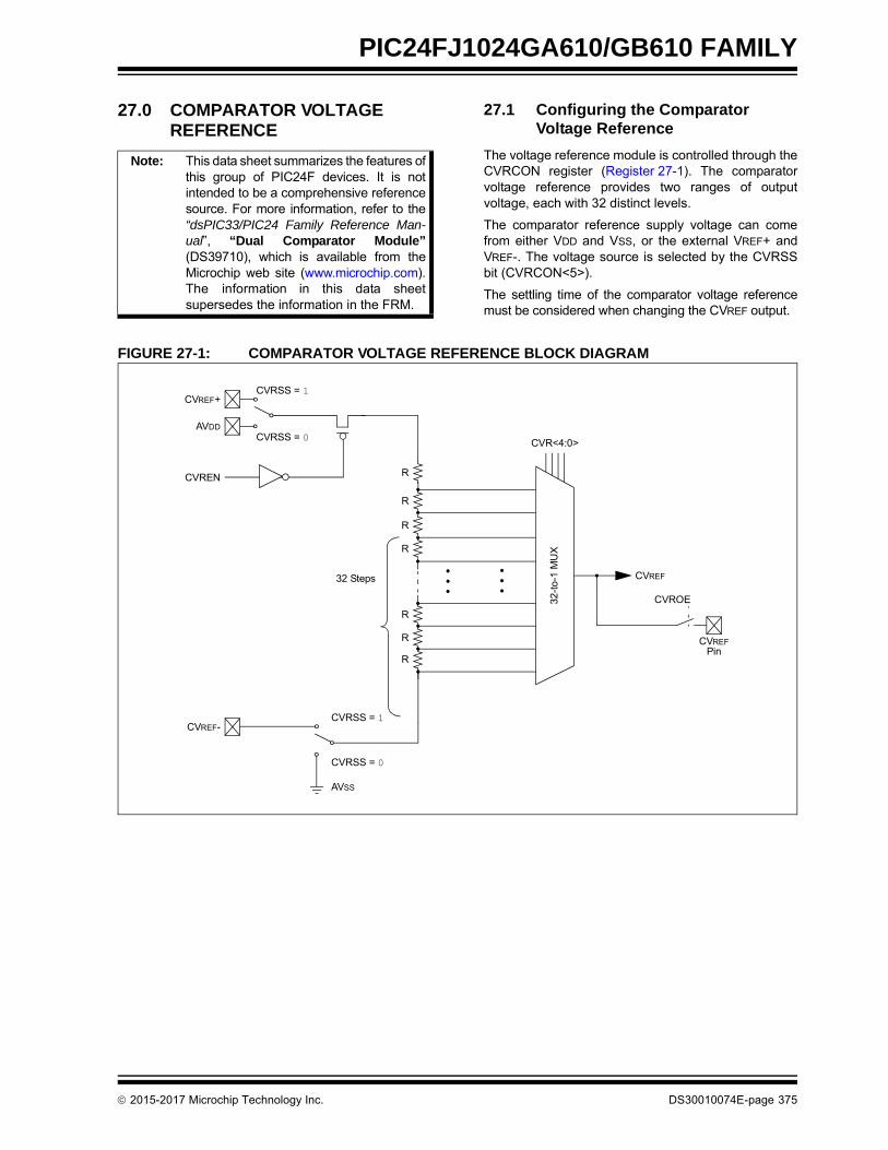
PIC24FJ1024GA610/GB610 FAMILY
27.0 COMPARATOR VOLTAGE REFERENCE
27.1 Configuring the Comparator Voltage Reference
The voltage reference module is controlled through theCVRCON register (Register 27-1). The comparatorvoltage reference provides two ranges of outputvoltage, each with 32 distinct levels.
The comparator reference supply voltage can comefrom either VDD and VSS, or the external VREF+ andVREF-. The voltage source is selected by the CVRSSbit (CVRCON<5>).
The settling time of the comparator voltage referencemust be considered when changing the CVREF output.
FIGURE 27-1: COMPARATOR VOLTAGE REFERENCE BLOCK DIAGRAM
Note: This data sheet summarizes the features ofthis group of PIC24F devices. It is notintended to be a comprehensive referencesource. For more information, refer to the“dsPIC33/PIC24 Family Reference Man-ual”, “Dual Comparator Module”(DS39710), which is available from theMicrochip web site (www.microchip.com).The information in this data sheetsupersedes the information in the FRM.
32-t
o-1
MU
X
CVR<4:0>
RCVREN
CVRSS = 0AVDD
CVREF+CVRSS = 1
CVRSS = 0
CVREF-CVRSS = 1
R
R
R
R
R
R
32 Steps CVREF
AVSS
CVROE
CVREFPin
2015-2017 Microchip Technology Inc. DS30010074E-page 375

PIC24FJ1024GA610/GB610 FAMILY
REGISTER 27-1: CVRCON: COMPARATOR VOLTAGE REFERENCE CONTROL REGISTER
U-0 U-0 U-0 U-0 U-0 R/W-0 R/W-0 R/W-0
— — — — — CVREFP CVREFM1 CVREFM0
bit 15 bit 8
R/W-0 R/W-0 R/W-0 R/W-0 R/W-0 R/W-0 R/W-0 R/W-0
CVREN CVROE CVRSS CVR4 CVR3 CVR2 CVR1 CVR0
bit 7 bit 0
Legend:
R = Readable bit W = Writable bit U = Unimplemented bit, read as ‘0’
-n = Value at POR ‘1’ = Bit is set ‘0’ = Bit is cleared x = Bit is unknown
bit 15-11 Unimplemented: Read as ‘0’
bit 10 CVREFP: Comparator Voltage Reference Select bit (valid only when CREF is ‘1’)
1 = CVREF+ is used as a reference voltage to the comparators0 = The CVR<4:0> bits (5-bit DAC) within this module provide the reference voltage to the comparators
bit 9-8 CVREFM<1:0>: Comparator Band Gap Reference Source Select bits (valid only when CCH<1:0> = 11)
00 = Band gap voltage is provided as an input to the comparators01 = Reserved10 = Reserved11 = CVREF+ is provided as an input to the comparators
bit 7 CVREN: Comparator Voltage Reference Enable bit
1 = CVREF circuit is powered on 0 = CVREF circuit is powered down
bit 6 CVROE: Comparator VREF Output Enable bit
1 = CVREF voltage level is output on the CVREF pin0 = CVREF voltage level is disconnected from the CVREF pin
bit 5 CVRSS: Comparator VREF Source Selection bit
1 = Comparator reference source, CVRSRC = CVREF+ – CVREF-0 = Comparator reference source, CVRSRC = AVDD – AVSS
bit 4-0 CVR<4:0>: Comparator VREF Value Selection 0 CVR<4:0> 31 bits
When CVRSS = 1:CVREF = (CVREF-) + (CVR<4:0>/32) (CVREF+ – CVREF-)
When CVRSS = 0:CVREF = (AVSS) + (CVR<4:0>/32) (AVDD – AVSS)
DS30010074E-page 376 2015-2017 Microchip Technology Inc.
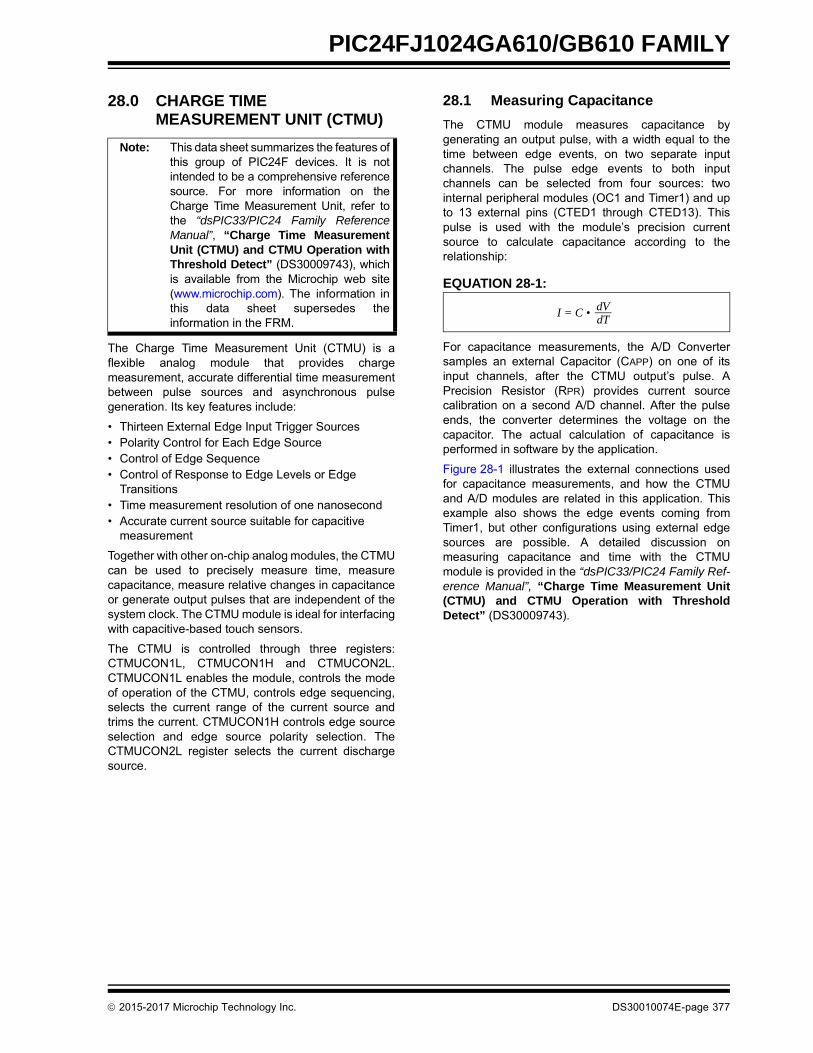
PIC24FJ1024GA610/GB610 FAMILY
28.0 CHARGE TIME MEASUREMENT UNIT (CTMU)
The Charge Time Measurement Unit (CTMU) is aflexible analog module that provides chargemeasurement, accurate differential time measurementbetween pulse sources and asynchronous pulsegeneration. Its key features include:
• Thirteen External Edge Input Trigger Sources• Polarity Control for Each Edge Source• Control of Edge Sequence• Control of Response to Edge Levels or Edge
Transitions• Time measurement resolution of one nanosecond• Accurate current source suitable for capacitive
measurement
Together with other on-chip analog modules, the CTMUcan be used to precisely measure time, measurecapacitance, measure relative changes in capacitanceor generate output pulses that are independent of thesystem clock. The CTMU module is ideal for interfacingwith capacitive-based touch sensors.
The CTMU is controlled through three registers:CTMUCON1L, CTMUCON1H and CTMUCON2L.CTMUCON1L enables the module, controls the modeof operation of the CTMU, controls edge sequencing,selects the current range of the current source andtrims the current. CTMUCON1H controls edge sourceselection and edge source polarity selection. TheCTMUCON2L register selects the current dischargesource.
28.1 Measuring Capacitance
The CTMU module measures capacitance bygenerating an output pulse, with a width equal to thetime between edge events, on two separate inputchannels. The pulse edge events to both inputchannels can be selected from four sources: twointernal peripheral modules (OC1 and Timer1) and upto 13 external pins (CTED1 through CTED13). Thispulse is used with the module’s precision currentsource to calculate capacitance according to therelationship:
EQUATION 28-1:
For capacitance measurements, the A/D Convertersamples an external Capacitor (CAPP) on one of itsinput channels, after the CTMU output’s pulse. APrecision Resistor (RPR) provides current sourcecalibration on a second A/D channel. After the pulseends, the converter determines the voltage on thecapacitor. The actual calculation of capacitance isperformed in software by the application.
Figure 28-1 illustrates the external connections usedfor capacitance measurements, and how the CTMUand A/D modules are related in this application. Thisexample also shows the edge events coming fromTimer1, but other configurations using external edgesources are possible. A detailed discussion onmeasuring capacitance and time with the CTMUmodule is provided in the “dsPIC33/PIC24 Family Ref-erence Manual”, “Charge Time Measurement Unit(CTMU) and CTMU Operation with ThresholdDetect” (DS30009743).
Note: This data sheet summarizes the features ofthis group of PIC24F devices. It is notintended to be a comprehensive referencesource. For more information on theCharge Time Measurement Unit, refer tothe “dsPIC33/PIC24 Family ReferenceManual”, “Charge Time MeasurementUnit (CTMU) and CTMU Operation withThreshold Detect” (DS30009743), whichis available from the Microchip web site(www.microchip.com). The information inthis data sheet supersedes theinformation in the FRM.
I = C • dVdT
2015-2017 Microchip Technology Inc. DS30010074E-page 377

PIC24FJ1024GA610/GB610 FAMILY
FIGURE 28-1: TYPICAL CONNECTIONS AND INTERNAL CONFIGURATION FOR CAPACITANCE MEASUREMENT
28.2 Measuring Time/Routing Current Source to A/D Input Pin
Time measurements on the pulse width can be similarlyperformed using the A/D module’s Internal Capacitor(CAD) and a precision resistor for current calibration.Figure 28-2 displays the external connections used fortime measurements, and how the CTMU and A/Dmodules are related in this application. This examplealso shows both edge events coming from the externalCTEDx pins, but other configurations using internaledge sources are possible.
This mode is enabled by clearing the TGEN bit(CTMUCON1L<12>). The current source is tied to theinput of the A/D after the sampling switch. Therefore,the A/D bit, SAMP, must be set to ‘1’ in order for thecurrent to be routed through the channel selection MUXto the desired pin.
28.3 Pulse Generation and Delay
The CTMU module can also generate an output pulsewith edges that are not synchronous with the device’ssystem clock. More specifically, it can generate a pulsewith a programmable delay from an edge event input tothe module.
When the module is configured for pulse generationdelay by setting the TGEN bit (CTMUCON1<12>), theinternal current source is connected to the B input ofComparator 2. A Capacitor (CDELAY) is connected tothe Comparator 2 pin, C2INB, and the ComparatorVoltage Reference, CVREF, is connected to C2INA.CVREF is then configured for a specific trip point. Themodule begins to charge CDELAY when an edge eventis detected. When CDELAY charges above the CVREF
trip point, a pulse is output on CTPLS. The length of thepulse delay is determined by the value of CDELAY andthe CVREF trip point.
Figure 28-3 illustrates the external connections forpulse generation, as well as the relationship of thedifferent analog modules required. While CTED1 isshown as the input pulse source, other options areavailable. A detailed discussion on pulse generationwith the CTMU module is provided in the “dsPIC33/PIC24 Family Reference Manual”.
PIC24F Device
A/D Converter
CTMU
ANx
CAPP
Output Pulse
EDG1
EDG2
RPR
ANy
Timer1
Current Source
DS30010074E-page 378 2015-2017 Microchip Technology Inc.

PIC24FJ1024GA610/GB610 FAMILY
FIGURE 28-2: TYPICAL CONNECTIONS AND INTERNAL CONFIGURATION FOR TIME MEASUREMENT (TGEN = 0)
FIGURE 28-3: TYPICAL CONNECTIONS AND INTERNAL CONFIGURATION FOR PULSE DELAY GENERATION (TGEN = 1)
PIC24F Device
A/D Converter
CTMU
CTEDx
CTEDx
ANx
Output Pulse
EDG1
EDG2
CAD
RPR
Current Source
C2
CVREF
CTPLS
PIC24F Device
Current Source
Comparator
CTMUCTEDx
C2INB
CDELAY
EDG1
–
2015-2017 Microchip Technology Inc. DS30010074E-page 379

PIC24FJ1024GA610/GB610 FAMILY
28.4 Measuring Die Temperature
The CTMU can be configured to use the A/D tomeasure the die temperature using dedicated A/DChannel 24. Perform the following steps to measurethe diode voltage:
• The internal current source must be set for either 5.5 µA (IRNG<1:0> = 0x2) or 55 µA (IRNG<1:0> = 0x3).
• In order to route the current source to the diode, the EDG1STAT and EDG2STAT bits must be equal (either both ‘0’ or both ‘1’).
• The CTMREQ bit (AD1CON5<13>) must be set to ‘1’.
• The A/D Channel Select bits must be 24 (0x18) using a single-ended measurement.
The voltage of the diode will vary over temperatureaccording to the graphs shown below (Figure 28-4). Notethat the graphs are different, based on the magnitude of
the current source selected. The slopes are nearly linearover the range of -40ºC to +100ºC and the temperaturecan be calculated as follows:
EQUATION 28-2:
FIGURE 28-4: DIODE VOLTAGE (mV) vs. DIE TEMPERATURE (TYPICAL)
710 mV – Vdiode1.8
Tdie =
760 mV – Vdiode1.55
Tdie =
For 5.5 µA Current Source:
where Vdiode is in mV, Tdie is in ºC
For 55 µA Current Source:
where Vdiode is in mV, Tdie is in ºC
450475500525550575600625650675700725750775800825850
-40 -20 0 20 40 60 80 100 120
5.5UA
55UA
Dio
de
Vo
lta
ge
(m
V)
Die Temperature (°C)
5.5 µA
55 µA
DS30010074E-page 380 2015-2017 Microchip Technology Inc.

PIC24FJ1024GA610/GB610 FAMILY
REGISTER 28-1: CTMUCON1L: CTMU CONTROL REGISTER 1 LOW
R/W-0 U-0 R/W-0 R/W-0 R/W-0 R/W-0 R/W-0 R/W-0
CTMUEN — CTMUSIDL TGEN EDGEN EDGSEQEN IDISSEN CTTRIG
bit 15 bit 8
R/W-0 R/W-0 R/W-0 R/W-0 R/W-0 R/W-0 R/W-0 R/W-0
ITRIM5 ITRIM4 ITRIM3 ITRIM2 ITRIM1 ITRIM0 IRNG1 IRNG0
bit 7 bit 0
Legend:
R = Readable bit W = Writable bit U = Unimplemented bit, read as ‘0’
-n = Value at POR ‘1’ = Bit is set ‘0’ = Bit is cleared x = Bit is unknown
bit 15 CTMUEN: CTMU Enable bit
1 = Module is enabled0 = Module is disabled
bit 14 Unimplemented: Read as ‘0’
bit 13 CTMUSIDL: CTMU Stop in Idle Mode bit
1 = Discontinues module operation when device enters Idle mode0 = Continues module operation in Idle mode
bit 12 TGEN: Time Generation Enable bit
1 = Enables edge delay generation and routes the current source to the comparator pin0 = Disables edge delay generation and routes the current source to the selected A/D input pin
bit 11 EDGEN: Edge Enable bit
1 = Edges are not blocked0 = Edges are blocked
bit 10 EDGSEQEN: Edge Sequence Enable bit
1 = Edge 1 event must occur before Edge 2 event can occur0 = No edge sequence is needed
bit 9 IDISSEN: Analog Current Source Control bit
1 = Analog current source output is grounded0 = Analog current source output is not grounded
bit 8 CTTRIG: CTMU Trigger Control bit
1 = Trigger output is enabled0 = Trigger output is disabled
bit 7-2 ITRIM<5:0>: Current Source Trim bits
011111 = Maximum positive change from nominal current011110•••000001 = Minimum positive change from nominal current000000 = Nominal current output specified by IRNG<1:0>111111 = Minimum negative change from nominal current•••100010100001 = Maximum negative change from nominal current
2015-2017 Microchip Technology Inc. DS30010074E-page 381

PIC24FJ1024GA610/GB610 FAMILY
bit 1-0 IRNG<1:0>: Current Source Range Select bits
If IRNGH = 0:11 = 55 µA range10 = 5.5 µA range01 = 550 nA range00 = 550 µA range
If IRNGH = 1:11 = Reserved10 = Reserved01 = 2.2 mA range00 = 550 µA range
REGISTER 28-1: CTMUCON1L: CTMU CONTROL REGISTER 1 LOW (CONTINUED)
DS30010074E-page 382 2015-2017 Microchip Technology Inc.

PIC24FJ1024GA610/GB610 FAMILY
REGISTER 28-2: CTMUCON1H: CTMU CONTROL REGISTER 1 HIGH
R/W-0 R/W-0 R/W-0 R/W-0 R/W-0 R/W-0 R/W-0 R/W-0
EDG1MOD EDG1POL EDG1SEL3 EDG1SEL2 EDG1SEL1 EDG1SEL0 EDG2STAT EDG1STAT
bit 15 bit 8
R/W-0 R/W-0 R/W-0 R/W-0 R/W-0 R/W-0 U-0 R/W-0
EDG2MOD EDG2POL EDG2SEL3 EDG2SEL2 EDG2SEL1 EDG2SEL0 — IRNGH
bit 7 bit 0
Legend:
R = Readable bit W = Writable bit U = Unimplemented bit, read as ‘0’
-n = Value at POR ‘1’ = Bit is set ‘0’ = Bit is cleared x = Bit is unknown
bit 15 EDG1MOD: Edge 1 Edge-Sensitive Select bit
1 = Input is edge-sensitive0 = Input is level-sensitive
bit 14 EDG1POL: Edge 1 Polarity Select bit
1 = Edge 1 is programmed for a positive edge response0 = Edge 1 is programmed for a negative edge response
bit 13-10 EDG1SEL<3:0>: Edge 1 Source Select bits
1111 = CMP C3OUT1110 = CMP C2OUT1101 = CMP C1OUT1100 = IC3 interrupt1011 = IC2 interrupt1010 = IC1 interrupt1001 = CTED8 pin1000 = CTED7 pin(1)
0111 = CTED6 pin0110 = CTED5 pin0101 = CTED4 pin0100 = CTED3 pin(1)
0011 = CTED1 pin0010 = CTED2 pin0001 = OC10000 = Timer1 match
bit 9 EDG2STAT: Edge 2 Status bit
Indicates the status of Edge 2 and can be written to control current source.1 = Edge 2 has occurred0 = Edge 2 has not occurred
bit 8 EDG1STAT: Edge 1 Status bit
Indicates the status of Edge 1 and can be written to control current source.1 = Edge 1 has occurred0 = Edge 1 has not occurred
bit 7 EDG2MOD: Edge 2 Edge-Sensitive Select bit
1 = Input is edge-sensitive0 = Input is level-sensitive
bit 6 EDG2POL: Edge 2 Polarity Select bit
1 = Edge 2 is programmed for a positive edge response0 = Edge 2 is programmed for a negative edge response
Note 1: CTED3, CTED7, CTED10 and CTED11 are not available on 64-pin packages.
2015-2017 Microchip Technology Inc. DS30010074E-page 383

PIC24FJ1024GA610/GB610 FAMILY
bit 5-2 EDG2SEL<3:0>: Edge 2 Source Select bits
1111 = CMP C3OUT1110 = CMP C2OUT1101 = CMP C1OUT1100 = Peripheral clock1011 = IC3 interrupt1010 = IC2 interrupt1001 = IC1 interrupt1000 = CTED13 pin0111 = CTED12 pin0110 = CTED11 pin(1)
0101 = CTED10 pin(1)
0100 = CTED9 pin0011 = CTED1 pin0010 = CTED2 pin0001 = OC10000 = Timer1 match
bit 1 Unimplemented: Read as ‘0’
bit 0 IRNGH: High-Current Range Select bit
1 = Uses the higher current ranges (550 µA-2.2 mA)0 = Uses the lower current ranges (550 nA-50 µA)Current output is set by the IRNG<1:0> bits in the CTMUCON1L register.
REGISTER 28-2: CTMUCON1H: CTMU CONTROL REGISTER 1 HIGH (CONTINUED)
Note 1: CTED3, CTED7, CTED10 and CTED11 are not available on 64-pin packages.
DS30010074E-page 384 2015-2017 Microchip Technology Inc.

PIC24FJ1024GA610/GB610 FAMILY
REGISTER 28-3: CTMUCON2L: CTMU CONTROL REGISTER 2 LOW
U-0 U-0 U-0 U-0 U-0 U-0 U-0 U-0
— — — — — — — —
bit 15 bit 8
U-0 U-0 U-0 R/W-0 U-0 R/W-0 R/W-0 R/W-0
— — — IRSTEN — DSCHS2 DSCHS1 DSCHS0
bit 7 bit 0
Legend:
R = Readable bit W = Writable bit U = Unimplemented bit, read as ‘0’
-n = Value at POR ‘1’ = Bit is set ‘0’ = Bit is cleared x = Bit is unknown
bit 15-5 Unimplemented: Read as ‘0’
bit 4 IRSTEN: CTMU Current Source Reset Enable bit
1 = Signal selected by DSCHS<2:0> bits or IDISSEN control bit will reset CTMU edge detect logic0 = CTMU edge detect logic will not occur
bit 3 Unimplemented: Read as ‘0’
bit 2-0 DSCHS<2:0>: Discharge Source Select bits
111 = CLC2 out110 = CLC1 out101 = Disabled100 = A/D end of conversion011 = MCCP3 auxiliary output010 = MCCP2 auxiliary output001 = MCCP1 auxiliary output000 = Disabled
2015-2017 Microchip Technology Inc. DS30010074E-page 385
PIC24FJ1024GA610/GB610 FAMILY
NOTES:
DS30010074E-page 386 2015-2017 Microchip Technology Inc.

PIC24FJ1024GA610/GB610 FAMILY
29.0 HIGH/LOW-VOLTAGE DETECT (HLVD)
The High/Low-Voltage Detect (HLVD) module is aprogrammable circuit that allows the user to specifyboth the device voltage trip point and the direction ofchange.
An interrupt flag is set if the device experiences anexcursion past the trip point in the direction of change.If the interrupt is enabled, the program execution willbranch to the interrupt vector address and the softwarecan then respond to the interrupt. The LVDIF flag maybe set during a POR or BOR event. The firmwareshould clear the flag before the application uses it forthe first time, even if the interrupt was disabled.
The HLVD Control register (see Register 29-1)completely controls the operation of the HLVD module.This allows the circuitry to be “turned off” by the userunder software control, which minimizes the currentconsumption for the device. The HLVDEN bit(HLVDCON<15>) should be cleared when writing datato the HLVDCON register. Once the register is config-ured, the module is enabled from power-down by settingHLVDEN. The application must wait a minimum of 5 µSbefore clearing the HLVDIF flag and using the moduleafter HLVDEN has been set.
FIGURE 29-1: HIGH/LOW-VOLTAGE DETECT (HLVD) MODULE BLOCK DIAGRAM
Note: This data sheet summarizes the featuresof this group of PIC24F devices. It isnot intended to be a comprehensivereference source. For more informationon the High/Low-Voltage Detect, refer tothe “dsPIC33/PIC24 Family ReferenceManual”, “High-Level Integrationwith Programmable High/Low-VoltageDetect (HLVD)” (DS39725), which isavailable from the Microchip web site(www.microchip.com). The information inthis data sheet supersedes theinformation in the FRM.
Set
VDD
16
-to
-1 M
UX
HLVDEN
HLVDL<3:0>HLVDIN
VDD
Externally GeneratedTrip Point
LVDIF
HLVDEN
Band Gap
VDIR
1.2V Typical
2015-2017 Microchip Technology Inc. DS30010074E-page 387
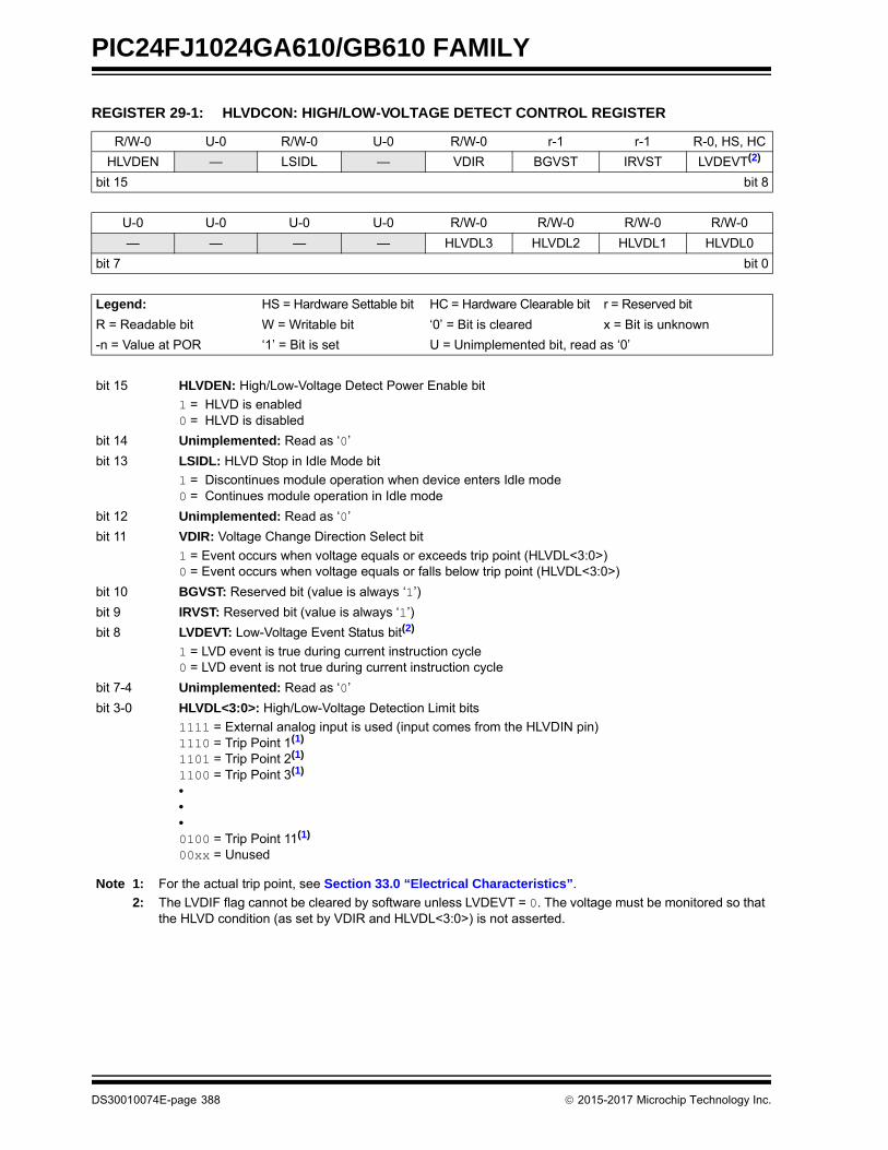
PIC24FJ1024GA610/GB610 FAMILY
REGISTER 29-1: HLVDCON: HIGH/LOW-VOLTAGE DETECT CONTROL REGISTER
R/W-0 U-0 R/W-0 U-0 R/W-0 r-1 r-1 R-0, HS, HC
HLVDEN — LSIDL — VDIR BGVST IRVST LVDEVT(2)
bit 15 bit 8
U-0 U-0 U-0 U-0 R/W-0 R/W-0 R/W-0 R/W-0
— — — — HLVDL3 HLVDL2 HLVDL1 HLVDL0
bit 7 bit 0
Legend: HS = Hardware Settable bit HC = Hardware Clearable bit r = Reserved bit
R = Readable bit W = Writable bit ‘0’ = Bit is cleared x = Bit is unknown
-n = Value at POR ‘1’ = Bit is set U = Unimplemented bit, read as ‘0’
bit 15 HLVDEN: High/Low-Voltage Detect Power Enable bit
1 = HLVD is enabled0 = HLVD is disabled
bit 14 Unimplemented: Read as ‘0’
bit 13 LSIDL: HLVD Stop in Idle Mode bit
1 = Discontinues module operation when device enters Idle mode0 = Continues module operation in Idle mode
bit 12 Unimplemented: Read as ‘0’
bit 11 VDIR: Voltage Change Direction Select bit
1 = Event occurs when voltage equals or exceeds trip point (HLVDL<3:0>)0 = Event occurs when voltage equals or falls below trip point (HLVDL<3:0>)
bit 10 BGVST: Reserved bit (value is always ‘1’)
bit 9 IRVST: Reserved bit (value is always ‘1’)
bit 8 LVDEVT: Low-Voltage Event Status bit(2)
1 = LVD event is true during current instruction cycle0 = LVD event is not true during current instruction cycle
bit 7-4 Unimplemented: Read as ‘0’
bit 3-0 HLVDL<3:0>: High/Low-Voltage Detection Limit bits
1111 = External analog input is used (input comes from the HLVDIN pin)1110 = Trip Point 1(1)
1101 = Trip Point 2(1)
1100 = Trip Point 3(1)
•••0100 = Trip Point 11(1)
00xx = Unused
Note 1: For the actual trip point, see Section 33.0 “Electrical Characteristics”.
2: The LVDIF flag cannot be cleared by software unless LVDEVT = 0. The voltage must be monitored so that the HLVD condition (as set by VDIR and HLVDL<3:0>) is not asserted.
DS30010074E-page 388 2015-2017 Microchip Technology Inc.
PIC24FJ1024GA610/GB610 FAMILY
30.0 SPECIAL FEATURES
PIC24FJ1024GA610/GB610 family devices includeseveral features intended to maximize applicationflexibility and reliability, and minimize cost throughelimination of external components. These are:
• Flexible Configuration
• Watchdog Timer (WDT)
• Code Protection
• JTAG Boundary Scan Interface
• In-Circuit Serial Programming™
• In-Circuit Emulation
30.1 Configuration Bits
The Configuration bits are stored in the last page loca-tion of implemented program memory. These bits can beset or cleared to select various device configurations.There are two types of Configuration bits: system oper-ation bits and code-protect bits. The system operationbits determine the power-on settings for system-levelcomponents, such as the oscillator and the WatchdogTimer. The code-protect bits prevent program memoryfrom being read and written.
In Dual Partition modes, each partition has its own set ofFlash Configuration Words. The full set of Configurationregisters in the Active Partition is used to determine thedevice’s configuration; the Configuration Words in theInactive Partition are used to determine the device’sconfiguration when that partition becomes active. How-ever, some of the Configuration registers in the InactivePartition (FSEC, FBSLIM and FSIGN) may be used todetermine how the Active Partition is able or allowed toaccess the Inactive Partition.
30.1.1 CONSIDERATIONS FOR CONFIGURING PIC24FJ1024GA610/GB610 FAMILY DEVICES
In PIC24FJ1024GA610/GB610 family devices, theConfiguration bytes are implemented as volatilememory. This means that configuration data must beprogrammed each time the device is powered up. Con-figuration data is stored in the three words at the top ofthe on-chip program memory space, known as theFlash Configuration Words. Their specific locations areshown in Table 30-1. The configuration data is auto-matically loaded from the Flash Configuration Words tothe proper Configuration registers during deviceResets. After a Reset, configuration reads areperformed in the following order:
• Device Calibration Information
• Partition Mode Configuration (FBOOT)
If Single Partition mode:
• User Configuration Words
If Dual Partition mode:
• Partition 1 Boot Sequence Number
• Partition 2 Boot Sequence Number
• User Configuration Words from the Active Partition
• Code Protection User Configuration Words from the Inactive Partition
When creating applications for these devices, usersshould always specifically allocate the location of theFlash Configuration Word for configuration data. This isto make certain that program code is not stored in thisaddress when the code is compiled.
The upper byte of all Flash Configuration Words in pro-gram memory should always be ‘0000 0000’. Thismakes them appear to be NOP instructions in theremote event that their locations are ever executed byaccident. Since Configuration bits are not implementedin the corresponding locations, writing ‘0’s to theselocations has no effect on device operation.
Note: This data sheet summarizes the features ofthis group of PIC24F devices. It is notintended to be a comprehensive referencesource. For more information, refer to thefollowing sections of the “dsPIC33/PIC24Family Reference Manual”, which areavailable from the Microchip web site(www.microchip.com). The information inthis data sheet supersedes theinformation in the FRM.
• “Watchdog Timer (WDT)” (DS39697)
• “High-Level Device Integration” (DS39719)
• “Programming and Diagnostics” (DS39716)
Note: Configuration data is reloaded on all typesof device Resets.
2015-2017 Microchip Technology Inc. DS30010074E-page 389

PIC24FJ1024GA610/GB610 FAMILY
TABLE 30-1: CONFIGURATION WORD ADDRESSES
Configuration Registers
Single Partition Mode
PIC24FJ1024GX6XX PIC24FJ512GX6XX PIC24FJ256GX6XX PIC24FJ128GX6XX
FSEC 0ABF00h 055F00h 02AF00h 015F00h
FBSLIM 0ABF10h 055F10h 02AF10h 015F10h
FSIGN 0ABF14h 055F14h 02AF14h 015F14h
FOSCSEL 0ABF18h 055F18h 02AF18h 015F18h
FOSC 0ABF1Ch 055F1Ch 02AF1Ch 015F1Ch
FWDT 0ABF20h 055F20h 02AF20h 015F20h
FPOR 0ABF24h 055F24h 02AF24h 015F24h
FICD 0ABF28h 055F28h 02AF28h 015F28h
FDEVOPT1 0ABF2Ch 055F2Ch 02AF2Ch 015F2Ch
FBOOT 801800h
Dual Partition Modes(1)
FSEC(2) 055F00h/455F00h 02AF00h/42AF00h 015700h/415700h 00AF00h/40AF00h
FBSLIM(2) 055F10h/455F10h 02AF10h/42AF10h 015710h/415710h 00AF10h/40AF10h
FSIGN(2) 055F14h/455F14h 02AF14h/42AF14h 015714h/ 415714h 00AF14h/40AF14h
FOSCSEL 055F18h/455F18h 02AF18h/42AF18h 015718h/415718h 00AF18h/40AF18h
FOSC 055F1Ch/455F1Ch 02AF1Ch/42AF1Ch 01571Ch/41571Ch 00AF1Ch/40AF1Ch
FWDT 055F20h/455F20h 02AF20h/42AF20h 015720h/415720h 00AF20h/40AF20h
FPOR 055F24h/ 455F24h 02AF24h/42AF24h 015724h/415724h 00AF24h/40AF24h
FICD 055F28h/455F28h 02AF28h/42AF28h 015728h/415728h 00AF28h/40AF28h
FDEVOPT1 055F2Ch/455F2Ch 02AF2Ch/42AF2Ch 01572Ch/41572Ch 00AF2Ch/40AF2Ch
FBTSEQ(3) 055FFCh/455FFCh 02AFFCh/42AFFCh 0157FCh/4157FCh 00AFFCh/40AFFCh
FBOOT 801800h
Note 1: Addresses shown for Dual Partition modes are for the Active/Inactive Partitions, respectively.
2: Changes to these Inactive Partition Configuration Words affect how the Active Partition accesses the Inactive Partition.
3: FBTSEQ is a 24-bit Configuration Word, using all three bytes of the program memory width.
DS30010074E-page 390 2015-2017 Microchip Technology Inc.

PIC24FJ1024GA610/GB610 FAMILY
REGISTER 30-1: FBOOT CONFIGURATION REGISTER
U-1 U-1 U-1 U-1 U-1 U-1 U-1 U-1
— — — — — — — —
bit 15 bit 8
U-1 U-1 U-1 U-1 U-1 U-1 R/PO-1 R/PO-1
— — — — — — BTMODE<1:0>
bit 7 bit 0
Legend: PO = Program Once bit
R = Readable bit W = Writable bit U = Unimplemented bit, read as ‘1’
-n = Value at POR ‘1’ = Bit is set ‘0’ = Bit is cleared x = Bit is unknown
bit 15-2 Unimplemented: Read as ‘1’
bit 1-0 BTMODE<1:0>: Device Partition Mode Configuration Status bits
11 = Single Partition mode10 = Dual Partition mode01 = Protected Dual Partition mode (Partition 1 is write-protected when inactive)00 = Reserved; do not use
REGISTER 30-2: FBTSEQ CONFIGURATION REGISTER
R/PO-1 R/PO-1 R/PO-1 R/PO-1 R/PO-1 R/PO-1 R/PO-1 R/PO-1
IBSEQ11 IBSEQ10 IBSEQ9 IBSEQ8 IBSEQ7 IBSEQ6 IBSEQ5 IBSEQ4
bit 23 bit 16
R/PO-1 R/PO-1 R/PO-1 R/PO-1 R/PO-1 R/PO-1 R/PO-1 R/PO-1
IBSEQ3 IBSEQ2 IBSEQ1 IBSEQ0 BSEQ11 BSEQ10 BSEQ9 BSEQ8
bit 15 bit 8
R/PO-1 R/PO-1 R/PO-1 R/PO-1 R/PO-1 R/PO-1 R/PO-1 R/PO-1
BSEQ7 BSEQ6 BSEQ5 BSEQ4 BSEQ3 BSEQ2 BSEQ1 BSEQ0
bit 7 bit 0
Legend: PO = Program Once bit
R = Readable bit W = Writable bit U = Unimplemented bit, read as ‘1’
-n = Value at POR ‘1’ = Bit is set ‘0’ = Bit is cleared x = Bit is unknown
bit 23-12 IBSEQ<11:0>: Inverse Boot Sequence Number bits (Dual Partition modes only)
The one’s complement of BSEQ<11:0>; must be calculated by the user and written into deviceprogramming.
bit 11-0 BSEQ<11:0>: Boot Sequence Number bits (Dual Partition modes only)
Relative value defining which partition will be active after a device Reset; the partition containing a lowerboot number will be active.
2015-2017 Microchip Technology Inc. DS30010074E-page 391

PIC24FJ1024GA610/GB610 FAMILY
REGISTER 30-3: FSEC CONFIGURATION REGISTER
U-1 U-1 U-1 U-1 U-1 U-1 U-1 U-1
— — — — — — — —
bit 23 bit 16
R/PO-1 U-1 U-1 U-1 R/PO-1 R/PO-1 R/PO-1 R/PO-1
AIVTDIS — — — CSS2 CSS1 CSS0 CWRP
bit 15 bit 8
R/PO-1 R/PO-1 R/PO-1 U-1 R/PO-1 R/PO-1 R/PO-1 R/PO-1
GSS1 GSS0 GWRP — BSEN BSS1 BSS0 BWRP
bit 7 bit 0
Legend: PO = Program Once bit
R = Readable bit W = Writable bit U = Unimplemented bit, read as ‘1’
-n = Value at POR ‘1’ = Bit is set ‘0’ = Bit is cleared x = Bit is unknown
bit 23-16 Unimplemented: Read as ‘1’
bit 15 AIVTDIS: Alternate Interrupt Vector Table Disable bit
1 = Disables AIVT; INTCON2<8> (AIVTEN) bit is not available0 = Enables AIVT; INTCON2<8> (AIVTEN) bit is available
bit 14-12 Unimplemented: Read as ‘1’
bit 11-9 CSS<2:0>: Configuration Segment Code Protection Level bits
111 = No protection (other than CWRP)110 = Standard security10x = Enhanced security0xx = High security
bit 8 CWRP: Configuration Segment Program Write Protection bit
1 = Configuration Segment is not write-protected0 = Configuration Segment is write-protected
bit 7-6 GSS<1:0>: General Segment Code Protection Level bits
11 = No protection (other than GWRP)10 = Standard security0x = High security
bit 5 GWRP: General Segment Program Write Protection bit
1 = General Segment is not write-protected0 = General Segment is write-protected
bit 4 Unimplemented: Read as ‘1’
bit 3 BSEN: Boot Segment Control bit
1 = No Boot Segment is enabled0 = Boot Segment size is determined by BSLIM<12:0>
bit 2-1 BSS<1:0>: Boot Segment Code Protection Level bits
11 = No protection (other than BWRP)10 = Standard security0x = High security
bit 0 BWRP: Boot Segment Program Write Protection bit
1 = Boot Segment can be written0 = Boot Segment is write-protected
DS30010074E-page 392 2015-2017 Microchip Technology Inc.

PIC24FJ1024GA610/GB610 FAMILY
REGISTER 30-4: FBSLIM CONFIGURATION REGISTER
U-1 U-1 U-1 U-1 U-1 U-1 U-1 U-1
— — — — — — — —
bit 23 bit 16
U-1 U-1 U-1 R/PO-1 R/PO-1 R/PO-1 R/PO-1 R/PO-1
— — — BSLIM<12:8>
bit 15 bit 8
R/PO-1 R/PO-1 R/PO-1 R/PO-1 R/PO-1 R/PO-1 R/PO-1 R/PO-1
BSLIM<7:0>
bit 7 bit 0
Legend: PO = Program Once bit
R = Readable bit W = Writable bit U = Unimplemented bit, read as ‘1’
-n = Value at POR ‘1’ = Bit is set ‘0’ = Bit is cleared x = Bit is unknown
bit 23-13 Unimplemented: Read as ‘1’
bit 12-0 BSLIM<12:0>: Active Boot Segment Code Flash Page Address Limit (Inverted) bits
This bit field contains the last active Boot Segment Page + 1 (i.e., first page address of GS). The valueis stored as an inverted page address, such that programming additional ‘0’s can only increase the sizeof BS. If BSLIM<12:0> is set to all ‘1’s (unprogrammed default), active Boot Segment size is zero.
2015-2017 Microchip Technology Inc. DS30010074E-page 393

PIC24FJ1024GA610/GB610 FAMILY
\
REGISTER 30-5: FSIGN CONFIGURATION REGISTER
U-1 U-1 U-1 U-1 U-1 U-1 U-1 U-1
— — — — — — — —
bit 23 bit 16
r-0 U-1 U-1 U-1 U-1 U-1 U-1 U-1
— — — — — — — —
bit 15 bit 8
U-1 U-1 U-1 U-1 U-1 U-1 U-1 U-1
— — — — — — — —
bit 7 bit 0
Legend: PO = Program Once bit r = Reserved bit
R = Readable bit W = Writable bit U = Unimplemented bit, read as ‘1’
-n = Value at POR ‘1’ = Bit is set ‘0’ = Bit is cleared x = Bit is unknown
bit 23-16 Unimplemented: Read as ‘1’
bit 15 Reserved: Maintain as ‘0’
bit 14-0 Unimplemented: Read as ‘1’
DS30010074E-page 394 2015-2017 Microchip Technology Inc.

PIC24FJ1024GA610/GB610 FAMILY
REGISTER 30-6: FOSCSEL CONFIGURATION REGISTER
U-1 U-1 U-1 U-1 U-1 U-1 U-1 U-1
— — — — — — — —
bit 23 bit 16
U-1 U-1 U-1 U-1 U-1 U-1 r-0 r-0
— — — — — — — —
bit 15 bit 8
R/PO-1 R/PO-1 R/PO-1 R/PO-1 R/PO-1 R/PO-1 R/PO-1 R/PO-1
IESO PLLMODE3 PLLMODE2 PLLMODE1 PLLMODE0 FNOSC2 FNOSC1 FNOSC0
bit 7 bit 0
Legend: PO = Program Once bit r = Reserved bit
R = Readable bit W = Writable bit U = Unimplemented bit, read as ‘1’
-n = Value at POR ‘1’ = Bit is set ‘0’ = Bit is cleared x = Bit is unknown
bit 23-10 Unimplemented: Read as ‘1’
bit 9-8 Reserved: Maintain as ‘0’
bit 7 IESO: Two-Speed Oscillator Start-up Enable bit
1 = Starts up the device with FRC, then automatically switches to the user-selected oscillator whenready
0 = Starts up the device with the user-selected oscillator source
bit 6-3 PLLMODE<3:0>: Frequency Multiplier Select bits
1111 = No PLL is used (PLLEN bit is unavailable)1110 = 8x PLL is selected1101 = 6x PLL is selected1100 = 4x PLL is selected0111 = 96 MHz USB PLL is selected (Input Frequency = 48 MHz)0110 = 96 MHz USB PLL is selected (Input Frequency = 32 MHz)0101 = 96 MHz USB PLL is selected (Input Frequency = 24 MHz)0100 = 96 MHz USB PLL is selected (Input Frequency = 20 MHz)0011 = 96 MHz USB PLL is selected (Input Frequency = 16 MHz)0010 = 96 MHz USB PLL is selected (Input Frequency = 12 MHz)0001 = 96 MHz USB PLL is selected (Input Frequency = 8 MHz)0000 = 96 MHz USB PLL is selected (Input Frequency = 4 MHz)
bit 2-0 FNOSC<2:0>: Oscillator Selection bits
111 = Oscillator with Frequency Divider (OSCFDIV)110 = Digitally Controlled Oscillator (DCO)101 = Low-Power RC Oscillator (LPRC)100 = Secondary Oscillator (SOSC)011 = Primary Oscillator with PLL (XTPLL, HSPLL, ECPLL)010 = Primary Oscillator (XT, HS, EC)001 = Fast RC Oscillator with PLL (FRCPLL)000 = Fast RC Oscillator (FRC)
2015-2017 Microchip Technology Inc. DS30010074E-page 395

PIC24FJ1024GA610/GB610 FAMILY
REGISTER 30-7: FOSC CONFIGURATION REGISTER
U-1 U-1 U-1 U-1 U-1 U-1 U-1 U-1
— — — — — — — —
bit 23 bit 16
U-1 U-1 U-1 U-1 U-1 U-1 U-1 U-1
— — — — — — — —
bit 15 bit 8
R/PO-1 R/PO-1 R/PO-1 R/PO-1 R/PO-1 R/PO-1 R/PO-1 R/PO-1
FCKSM1 FCKSM0 IOL1WAY PLLSS(1) SOSCSEL OSCIOFCN POSCMD1 POSCMD0
bit 7 bit 0
Legend: PO = Program Once bit
R = Readable bit W = Writable bit U = Unimplemented bit, read as ‘1’
-n = Value at POR ‘1’ = Bit is set ‘0’ = Bit is cleared x = Bit is unknown
bit 23-8 Unimplemented: Read as ‘1’
bit 7-6 FCKSM<1:0>: Clock Switching and Monitor Selection bits
1x = Clock switching and the Fail-Safe Clock Monitor are disabled01 = Clock switching is enabled, Fail-Safe Clock Monitor is disabled00 = Clock switching and the Fail-Safe Clock Monitor are enabled
bit 5 IOL1WAY: Peripheral Pin Select Configuration bit
1 = The IOLOCK bit can be set only once (with unlock sequence).0 = The IOLOCK bit can be set and cleared as needed (with unlock sequence)
bit 4 PLLSS: PLL Source Selection Configuration bit(1)
1 = PLL is fed by the Primary Oscillator (EC, XT or HS mode)0 = PLL is fed by the on-chip Fast RC (FRC) Oscillator
bit 3 SOSCSEL: SOSC Selection Configuration bit
1 = Crystal (SOSCI/SOSCO) mode0 = Digital (SOSCI) mode
bit 2 OSCIOFCN: CLKO Enable Configuration bit
1 = CLKO output signal is active on the OSCO pin (when the Primary Oscillator is disabled or configuredfor EC mode)
0 = CLKO output is disabled
bit 1-0 POSCMD<1:0>: Primary Oscillator Configuration bits
11 = Primary Oscillator mode is disabled10 = HS Oscillator mode is selected (10 MHz-32 MHz)01 = XT Oscillator mode is selected (1.5 MHz-10 MHz)00 = External Clock mode is selected
Note 1: When the primary clock source is greater than 8 MHz, this bit must be set to ‘0’ to prevent overclocking the PLL.
DS30010074E-page 396 2015-2017 Microchip Technology Inc.

PIC24FJ1024GA610/GB610 FAMILY
REGISTER 30-8: FWDT CONFIGURATION REGISTER
U-1 U-1 U-1 U-1 U-1 U-1 U-1 U-1
— — — — — — — —
bit 23 bit 16
U-1 R/PO-1 R/PO-1 U-1 R/PO-1 U-1 R/PO-1 R/PO-1
— WDTCLK1 WDTCLK0 — WDTCMX — WDTWIN1 WDTWIN0
bit 15 bit 8
R/PO-1 R/PO-1 R/PO-1 R/PO-1 R/PO-1 R/PO-1 R/PO-1 R/PO-1
WINDIS FWDTEN1 FWDTEN0 FWPSA WDTPS3 WDTPS2 WDTPS1 WDTPS0
bit 7 bit 0
Legend: PO = Program Once bit
R = Readable bit W = Writable bit U = Unimplemented bit, read as ‘1’
-n = Value at POR ‘1’ = Bit is set ‘0’ = Bit is cleared x = Bit is unknown
bit 23-15 Unimplemented: Read as ‘1’
bit 14-13 WDTCLK<1:0>: Watchdog Timer Clock Select bits (when WDTCMX = 1)
11 = Always uses LPRC10 = Uses FRC when WINDIS = 0, system clock is not LPRC and device is not in Sleep; otherwise,
uses LPRC01 = Always uses SOSC00 = Uses peripheral clock when system clock is not LPRC and device is not in Sleep; otherwise, uses
LPRC
bit 12 Unimplemented: Read as ‘1’
bit 11 WDTCMX: WDT Clock MUX Control bit
1 = Enables WDT clock MUX; WDT clock is selected by WDTCLK<1:0>0 = WDT clock is LPRC
bit 10 Unimplemented: Read as ‘1’
bit 9-8 WDTWIN<1:0>: Watchdog Timer Window Width bits
11 = WDT window is 25% of the WDT period10 = WDT window is 37.5% of the WDT period01 = WDT window is 50% of the WDT period00 = WDT window is 75% of the WDT period
bit 7 WINDIS: Windowed Watchdog Timer Disable bit
1 = Windowed WDT is disabled0 = Windowed WDT is enabled
bit 6-5 FWDTEN<1:0>: Watchdog Timer Enable bits
11 = WDT is enabled10 = WDT is disabled (control is placed on the SWDTEN bit)01 = WDT is enabled only while device is active and disabled in Sleep; SWDTEN bit is disabled00 = WDT and SWDTEN are disabled
bit 4 FWPSA: Watchdog Timer Prescaler bit
1 = WDT prescaler ratio of 1:1280 = WDT prescaler ratio of 1:32
2015-2017 Microchip Technology Inc. DS30010074E-page 397

PIC24FJ1024GA610/GB610 FAMILY
bit 3-0 WDTPS<3:0>: Watchdog Timer Postscale Select bits
1111 = 1:32,7681110 = 1:16,3841101 = 1:8,1921100 = 1:4,0961011 = 1:2,0481010 = 1:1,0241001 = 1:5121000 = 1:2560111 = 1:1280110 = 1:640101 = 1:320100 = 1:160011 = 1:80010 = 1:40001 = 1:20000 = 1:1
REGISTER 30-8: FWDT CONFIGURATION REGISTER (CONTINUED)
DS30010074E-page 398 2015-2017 Microchip Technology Inc.

PIC24FJ1024GA610/GB610 FAMILY
REGISTER 30-9: FPOR CONFIGURATION REGISTER
U-1 U-1 U-1 U-1 U-1 U-1 U-1 U-1
— — — — — — — —
bit 23 bit 16
U-1 U-1 U-1 U-1 U-1 U-1 U-1 U-1
— — — — — — — —
bit 15 bit 8
U-1 U-1 U-1 U-1 R/PO-1 R/PO-1 R/PO-1 R/PO-1
— — — — DNVPEN LPCFG BOREN1 BOREN0
bit 7 bit 0
Legend: PO = Program Once bit
R = Readable bit W = Writable bit U = Unimplemented bit, read as ‘1’
-n = Value at POR ‘1’ = Bit is set ‘0’ = Bit is cleared x = Bit is unknown
bit 23-4 Unimplemented: Read as ‘1’
bit 3 DNVPEN: Downside Voltage Protection Enable bit
1 = Downside protection is enabled when BOR is inactive; POR can be re-armed as needed (can resultin extra POR monitoring current once POR is re-armed)
0 = Downside protection is disabled when BOR is inactive
bit 2 LPCFG: Low-Power Regulator Control bit
1 = Retention feature is not available0 = Retention feature is available and controlled by RETEN during Sleep
bit 1-0 BOREN<1:0>: Brown-out Reset Enable bits
11 = Brown-out Reset is enabled in hardware; SBOREN bit is disabled10 = Brown-out Reset is enabled only while device is active and is disabled in Sleep; SBOREN bit is
disabled01 = Brown-out Reset is controlled with the SBOREN bit setting00 = Brown-out Reset is disabled in hardware; SBOREN bit is disabled
2015-2017 Microchip Technology Inc. DS30010074E-page 399

PIC24FJ1024GA610/GB610 FAMILY
REGISTER 30-10: FICD CONFIGURATION REGISTER
U-1 U-1 U-1 U-1 U-1 U-1 U-1 U-1
— — — — — — — —
bit 23 bit 16
R/PO-1 U-1 U-1 U-1 U-1 U-1 U-1 U-1
BTSWP — — — — — — —
bit 15 bit 8
r-1 U-1 R/PO-1 U-1 U-1 U-1 R/PO-1 R/PO-1
— — JTAGEN — — — ICS1 ICS0
bit 7 bit 0
Legend: PO = Program Once bit r = Reserved bit
R = Readable bit W = Writable bit U = Unimplemented bit, read as ‘1’
-n = Value at POR ‘1’ = Bit is set ‘0’ = Bit is cleared x = Bit is unknown
bit 23-16 Unimplemented: Read as ‘1’
bit 15 BTSWP: BOOTSWP Instruction Enable bit
1 = BOOTSWP instruction is disabled0 = BOOTSWP instruction is enabled
bit 14-8 Unimplemented: Read as ‘1’
bit 7 Reserved: Maintain as ‘1’
bit 6 Unimplemented: Read as ‘1’
bit 5 JTAGEN: JTAG Port Enable bit
1 = JTAG port is enabled0 = JTAG port is disabled
bit 4-2 Unimplemented: Read as ‘1’
bit 1-0 ICS<1:0>: ICD Communication Channel Select bits
11 = Communicates on PGEC1/PGED110 = Communicates on PGEC2/PGED201 = Communicates on PGEC3/PGED300 = Reserved; do not use
DS30010074E-page 400 2015-2017 Microchip Technology Inc.

PIC24FJ1024GA610/GB610 FAMILY
REGISTER 30-11: FDEVOPT1 CONFIGURATION REGISTER
U-1 U-1 U-1 U-1 U-1 U-1 U-1 U-1
— — — — — — — —
bit 23 bit 16
U-1 U-1 U-1 U-1 U-1 U-1 U-1 U-1
— — — — — — — —
bit 15 bit 8
U-1 U-1 U-1 R/PO-1 R/PO-1 R/PO-1 R/PO-1 U-1
— — — ALTVREF SOSCHP(1) TMPRPIN ALTCMPI —
bit 7 bit 0
Legend: PO = Program Once bit
R = Readable bit W = Writable bit U = Unimplemented bit, read as ‘1’
-n = Value at POR ‘1’ = Bit is set ‘0’ = Bit is cleared x = Bit is unknown
bit 23-5 Unimplemented: Read as ‘1’
bit 4 ALTVREF: Alternate Voltage Reference Location Enable bit (100-pin and 121-pin devices only)
1 = VREF+ and CVREF+ on RA10, VREF- and CVREF- on RA90 = VREF+ and CVREF+ on RB0, VREF- and CVREF- on RB1
bit 3 SOSCHP: SOSC High-Power Enable bit (valid only when SOSCSEL = 1)(1)
1 = SOSC High-Power mode is enabled0 = SOSC Low-Power mode is enabled
bit 2 TMPRPIN: Tamper Pin Enable bit
1 = TMPR pin function is disabled0 = TMPR pin function is enabled
bit 1 ALTCMPI: Alternate Comparator Input Enable bit
1 = C1INC, C2INC and C3INC are on their standard pin locations0 = C1INC, C2INC and C3INC are on RG9
bit 0 Unimplemented: Read as ‘1’
Note 1: High-Power mode is for crystals with 35K ESR (typical). Low-Power mode is for crystals with more than 65K ESR.
2015-2017 Microchip Technology Inc. DS30010074E-page 401

PIC24FJ1024GA610/GB610 FAMILY
TABLE 30-2: DEVICE ID REGISTERS
TABLE 30-3: DEVICE ID BIT FIELD DESCRIPTIONS
TABLE 30-4: PIC24FJ1024GA610/GB610 FAMILY DEVICE IDs
30.2 Unique Device Identifier (UDID)
All PIC24FJ1024GA610/GB610 family devices areindividually encoded during final manufacturing with aUnique Device Identifier, or UDID. The UDID cannot beerased by a bulk erase command or any other user-accessible means. This feature allows for manufacturingtraceability of Microchip Technology devices in applica-tions where this is a requirement. It may also be used bythe application manufacturer for any number of thingsthat may require unique identification, such as:
• Tracking the device
• Unique serial number
• Unique security key
The UDID comprises five 24-bit program words. Whentaken together, these fields form a unique 120-bitidentifier.
The UDID is stored in five read-only locations, locatedbetween 801600h and 801608h in the device configu-ration space. Table 30-5 lists the addresses of theidentifier words.
Address NameBit
15 14 13 12 11 10 9 8 7 6 5 4 3 2 1 0
FF0000h DEVID FAMID<7:0> DEV<7:0>
FF0002h DEVREV — REV<3:0>
Bit Field Register Description
FAMID<7:0> DEVID Encodes the family ID of the device.
DEV<7:0> DEVID Encodes the individual ID of the device.
REV<3:0> DEVREV Encodes the sequential (numerical) revision identifier of the device.
Device DEVID
PIC24FJ128GA606 6000h
PIC24FJ256GA606 6008h
PIC24FJ512GA606 6010h
PIC24FJ1024GA606 6018h
PIC24FJ128GA610 6001h
PIC24FJ256GA610 6009h
PIC24FJ512GA610 6011h
PIC24FJ1024GA610 6019h
PIC24FJ128GB606 6004h
PIC24FJ256GB606 600Ch
PIC24FJ512GB606 6014h
PIC24FJ1024GB606 601Ch
PIC24FJ128GB610 6005h
PIC24FJ256GB610 600Dh
PIC24FJ512GB610 6015h
PIC24FJ1024GB610 601Dh
TABLE 30-5: UDID ADDRESSES
UDID Address Description
UDID1 801600 UDID Word 1
UDID2 801602 UDID Word 2
UDID3 801604 UDID Word 3
UDID4 801606 UDID Word 4
UDID5 801608 UDID Word 5
DS30010074E-page 402 2015-2017 Microchip Technology Inc.

PIC24FJ1024GA610/GB610 FAMILY
30.3 On-Chip Voltage Regulator
All PIC24FJ1024GA610/GB610 family devices powertheir core digital logic at a nominal 1.8V. This maycreate an issue for designs that are required to operateat a higher typical voltage, such as 3.3V. To simplifysystem design, all devices in the PIC24FJ1024GA610/GB610 family incorporate an on-chip regulator thatallows the device to run its core logic from VDD.
This regulator is always enabled. It provides a constantvoltage (1.8V nominal) to the digital core logic, from aVDD of about 2.1V, all the way up to the device’sVDDMAX. It does not have the capability to boost VDD
levels. In order to prevent “brown-out” conditions whenthe voltage drops too low for the regulator, the Brown-out Reset occurs. Then, the regulator output followsVDD with a typical voltage drop of 300 mV.
A low-ESR capacitor (such as ceramic) must beconnected to the VCAP pin (Figure 30-1). This helps tomaintain the stability of the regulator. The recommendedvalue for the filter capacitor (CEFC) is provided inSection 33.1 “DC Characteristics”.
FIGURE 30-1: CONNECTIONS FOR THE ON-CHIP REGULATOR
30.3.1 ON-CHIP REGULATOR AND POR
The voltage regulator takes approximately 10 s for itto generate output. During this time, designated asTVREG, code execution is disabled. TVREG is appliedevery time the device resumes operation after anypower-down, including Sleep mode. TVREG is deter-mined by the status of the VREGS bit (RCON<8>) andthe WDTWIN<1:0> Configuration bits (FWDT<9:8>).Refer to Section 33.0 “Electrical Characteristics” formore information on TVREG.
30.3.2 VOLTAGE REGULATOR STANDBY MODE
The on-chip regulator always consumes a small incre-mental amount of current over IDD/IPD, including whenthe device is in Sleep mode, even though the coredigital logic does not require power. To provide addi-tional savings in applications where power resourcesare critical, the regulator can be made to enter Standbymode on its own whenever the device goes into Sleepmode. This feature is controlled by the VREGS bit(RCON<8>). Clearing the VREGS bit enables theStandby mode. When waking up from Standby mode,the regulator needs to wait for TVREG to expire beforewake-up.
30.3.3 LOW-VOLTAGE/RETENTION REGULATOR
When in Sleep mode, PIC24FJ1024GA610/GB610family devices may use a separate low-power, low-voltage/retention regulator to power critical circuits.This regulator, which operates at 1.2V nominal, main-tains power to data RAM and the RTCC while all othercore digital logic is powered down. The low-voltage/retention regulator is described in more detail inSection 10.2.4 “Low-Voltage Retention Regulator”.
VDD
VCAP
VSS
PIC24FJXXXGX6XX
CEFC
3.3V(1)
Note 1: This is a typical operating voltage. Refer to Section 33.0 “Electrical Characteristics” for the full operating ranges of VDD.
(10 F typ)
Note: For more information, see Section 33.0“Electrical Characteristics”. The infor-mation in this data sheet supersedes theinformation in the FRM.
2015-2017 Microchip Technology Inc. DS30010074E-page 403
PIC24FJ1024GA610/GB610 FAMILY
30.4 Watchdog Timer (WDT)
For PIC24FJ1024GA610/GB610 family devices, theWDT is driven by the LPRC Oscillator, the SecondaryOscillator (SOSC) or the system timer. When the deviceis in Sleep mode, the LPRC Oscillator will be used. Whenthe WDT is enabled, the clock source is also enabled.
The nominal WDT clock source from LPRC is 31 kHz.This feeds a prescaler that can be configured for either5-bit (divide-by-32) or 7-bit (divide-by-128) operation.The prescaler is set by the FWPSA Configuration bit.With a 31 kHz input, the prescaler yields a nominalWDT Time-out (TWDT) period of 1 ms in 5-bit mode or4 ms in 7-bit mode.
A variable postscaler divides down the WDT prescaleroutput and allows for a wide range of time-out periods.The postscaler is controlled by the WDTPS<3:0> Con-figuration bits (FWDT<3:0>), which allows the selectionof a total of 16 settings, from 1:1 to 1:32,768. Using theprescaler and postscaler time-out periods, ranges from1 ms to 131 seconds, can be achieved.
The WDT, prescaler and postscaler are reset:
• On any device Reset
• On the completion of a clock switch, whether invoked by software (i.e., setting the OSWEN bit after changing the NOSCx bits) or by hardware (i.e., Fail-Safe Clock Monitor)
• When a PWRSAV instruction is executed (i.e., Sleep or Idle mode is entered)
• When the device exits Sleep or Idle mode to resume normal operation
• By a CLRWDT instruction during normal execution
If the WDT is enabled, it will continue to run duringSleep or Idle modes. When the WDT time-out occurs,the device will wake the device and code execution willcontinue from where the PWRSAV instruction wasexecuted. The corresponding SLEEP or IDLE(RCON<3:2>) bits will need to be cleared in softwareafter the device wakes up.
The WDT Flag bit, WDTO (RCON<4>), is not auto-matically cleared following a WDT time-out. To detectsubsequent WDT events, the flag must be cleared insoftware.
30.4.1 WINDOWED OPERATION
The Watchdog Timer has an optional Fixed Windowmode of operation. In this Windowed mode, CLRWDTinstructions can only reset the WDT during the last 1/4of the programmed WDT period. A CLRWDT instructionexecuted before that window causes a WDT Reset,similar to a WDT time-out.
Windowed WDT mode is enabled by programming theWINDIS Configuration bit (FWDT<7>) to ‘0’.
30.4.2 CONTROL REGISTER
The WDT is enabled or disabled by the FWDTEN<1:0>Configuration bits (FWDT<6:5>). When the Configura-tion bits, FWDTEN<1:0> = 11, the WDT is alwaysenabled.
The WDT can be optionally controlled in software whenthe Configuration bits, FWDTEN<1:0> = 10. WhenFWDTEN<1:0> = 00, the Watchdog Timer is alwaysdisabled. The WDT is enabled in software by settingthe SWDTEN control bit (RCON<5>). The SWDTENcontrol bit is cleared on any device Reset. The softwareWDT option allows the user to enable the WDT forcritical code segments and disable the WDT duringnon-critical code segments for maximum power savings.
Note: The CLRWDT and PWRSAV instructionsclear the prescaler and postscaler countswhen executed.
DS30010074E-page 404 2015-2017 Microchip Technology Inc.

PIC24FJ1024GA610/GB610 FAMILY
FIGURE 30-2: WDT BLOCK DIAGRAM
WDT Overflow
Wake from
31 kHz
Prescaler Postscaler
FWPSA
SWDTENFWDTEN<1:0>
Reset
Sleep or Idle Mode
LPRC Control
(5-bit/7-bit) 1:1 to 1:32.768
WDTPS<3:0>
1 ms/4 ms
WDTCounter
SOSC
FRC
Peripheral Clock
WDTCLKS<1:0>
LPRC
WINDIS
System Clock (LRPC)
Sleep
CLRWDT Instr.PWRSAV Instr.
All Device Resets
Transition to NewClock Source
Exit Sleep orIdle Mode
2015-2017 Microchip Technology Inc. DS30010074E-page 405

PIC24FJ1024GA610/GB610 FAMILY
30.5 Program Verification and Code Protection
PIC24FJ1024GA610/GB610 family devices offer basicimplementation of CodeGuard™ Security that supportsGeneral Segment (GS) security and Boot Segment(BS) security. This feature helps protect individualIntellectual Property.
30.6 JTAG Interface
PIC24FJ1024GA610/GB610 family devices implementa JTAG interface, which supports boundary scandevice testing.
30.7 In-Circuit Serial Programming
PIC24FJ1024GA610/GB610 family microcontrollerscan be serially programmed while in the end applica-tion circuit. This is simply done with two lines for clock(PGECx) and data (PGEDx), and three other lines forpower (VDD), ground (VSS) and MCLR. This allowscustomers to manufacture boards with unprogrammeddevices and then program the microcontroller justbefore shipping the product. This also allows themost recent firmware or a custom firmware to beprogrammed.
30.8 Customer OTP Memory
PIC24FJ1024GA610/GB610 family devices provide256 bytes of One-Time-Programmable (OTP) memory,located at addresses, 801700h through 8017FEh. Thismemory can be used for persistent storage ofapplication-specific information that will not be erasedby reprogramming the device. This includes manytypes of information, such as (but not limited to):
• Application checksums
• Code revision information
• Product information
• Serial numbers
• System manufacturing dates
• Manufacturing lot numbers
OTP memory can be written by program execution (i.e.,TBLWT instructions), and during device programming.Data is not cleared by a chip erase.
30.9 In-Circuit Debugger
This function allows simple debugging functions whenused with MPLAB IDE. Debugging functionality is con-trolled through the PGECx (Emulation/Debug Clock)and PGEDx (Emulation/Debug Data) pins.
To use the in-circuit debugger function of the device,the design must implement ICSP™ connections toMCLR, VDD, VSS and the PGECx/PGEDx pin pair, des-ignated by the ICS<1:0> Configuration bits. In addition,when the feature is enabled, some of the resources arenot available for general use. These resources includethe first 80 bytes of data RAM and two I/O pins.
Note: For more information on usage, configura-tion and operation, refer to the “dsPIC33/PIC24 Family Reference Manual”,“CodeGuard™ Intermediate Security”(DS70005182).
Note: Data in the OTP memory section MUSTNOT be programmed more than once.
DS30010074E-page 406 2015-2017 Microchip Technology Inc.

PIC24FJ1024GA610/GB610 FAMILY
31.0 DEVELOPMENT SUPPORT
The PIC® microcontrollers (MCU) and dsPIC® digitalsignal controllers (DSC) are supported with a full rangeof software and hardware development tools:
• Integrated Development Environment
- MPLAB® X IDE Software
• Compilers/Assemblers/Linkers
- MPLAB XC Compiler
- MPASMTM Assembler
- MPLINKTM Object Linker/MPLIBTM Object Librarian
- MPLAB Assembler/Linker/Librarian forVarious Device Families
• Simulators
- MPLAB X SIM Software Simulator
• Emulators
- MPLAB REAL ICE™ In-Circuit Emulator
• In-Circuit Debuggers/Programmers
- MPLAB ICD 3
- PICkit™ 3
• Device Programmers
- MPLAB PM3 Device Programmer
• Low-Cost Demonstration/Development Boards, Evaluation Kits and Starter Kits
• Third-party development tools
31.1 MPLAB X Integrated Development Environment Software
The MPLAB X IDE is a single, unified graphical userinterface for Microchip and third-party software, andhardware development tool that runs on Windows®,Linux and Mac OS® X. Based on the NetBeans IDE,MPLAB X IDE is an entirely new IDE with a host of freesoftware components and plug-ins for high-performance application development and debugging.Moving between tools and upgrading from softwaresimulators to hardware debugging and programmingtools is simple with the seamless user interface.
With complete project management, visual call graphs,a configurable watch window and a feature-rich editorthat includes code completion and context menus,MPLAB X IDE is flexible and friendly enough for newusers. With the ability to support multiple tools onmultiple projects with simultaneous debugging, MPLABX IDE is also suitable for the needs of experiencedusers.
Feature-Rich Editor:
• Color syntax highlighting
• Smart code completion makes suggestions and provides hints as you type
• Automatic code formatting based on user-defined rules
• Live parsing
User-Friendly, Customizable Interface:
• Fully customizable interface: toolbars, toolbar buttons, windows, window placement, etc.
• Call graph window
Project-Based Workspaces:
• Multiple projects
• Multiple tools
• Multiple configurations
• Simultaneous debugging sessions
File History and Bug Tracking:
• Local file history feature
• Built-in support for Bugzilla issue tracker
2015-2017 Microchip Technology Inc. DS30010074E-page 407

PIC24FJ1024GA610/GB610 FAMILY
31.2 MPLAB XC Compilers
The MPLAB XC Compilers are complete ANSI Ccompilers for all of Microchip’s 8, 16, and 32-bit MCUand DSC devices. These compilers provide powerfulintegration capabilities, superior code optimization andease of use. MPLAB XC Compilers run on Windows,Linux or MAC OS X.
For easy source level debugging, the compilers providedebug information that is optimized to the MPLAB XIDE.
The free MPLAB XC Compiler editions support alldevices and commands, with no time or memoryrestrictions, and offer sufficient code optimization formost applications.
MPLAB XC Compilers include an assembler, linker andutilities. The assembler generates relocatable objectfiles that can then be archived or linked with other relo-catable object files and archives to create an execut-able file. MPLAB XC Compiler uses the assembler toproduce its object file. Notable features of the assem-bler include:
• Support for the entire device instruction set
• Support for fixed-point and floating-point data
• Command-line interface
• Rich directive set
• Flexible macro language
• MPLAB X IDE compatibility
31.3 MPASM Assembler
The MPASM Assembler is a full-featured, universalmacro assembler for PIC10/12/16/18 MCUs.
The MPASM Assembler generates relocatable objectfiles for the MPLINK Object Linker, Intel® standard HEXfiles, MAP files to detail memory usage and symbolreference, absolute LST files that contain source linesand generated machine code, and COFF files fordebugging.
The MPASM Assembler features include:
• Integration into MPLAB X IDE projects
• User-defined macros to streamline assembly code
• Conditional assembly for multipurpose source files
• Directives that allow complete control over the assembly process
31.4 MPLINK Object Linker/MPLIB Object Librarian
The MPLINK Object Linker combines relocatableobjects created by the MPASM Assembler. It can linkrelocatable objects from precompiled libraries, usingdirectives from a linker script.
The MPLIB Object Librarian manages the creation andmodification of library files of precompiled code. Whena routine from a library is called from a source file, onlythe modules that contain that routine will be linked inwith the application. This allows large libraries to beused efficiently in many different applications.
The object linker/library features include:
• Efficient linking of single libraries instead of many smaller files
• Enhanced code maintainability by grouping related modules together
• Flexible creation of libraries with easy module listing, replacement, deletion and extraction
31.5 MPLAB Assembler, Linker and Librarian for Various Device Families
MPLAB Assembler produces relocatable machinecode from symbolic assembly language for PIC24,PIC32 and dsPIC DSC devices. MPLAB XC Compileruses the assembler to produce its object file. Theassembler generates relocatable object files that canthen be archived or linked with other relocatable objectfiles and archives to create an executable file. Notablefeatures of the assembler include:
• Support for the entire device instruction set
• Support for fixed-point and floating-point data
• Command-line interface
• Rich directive set
• Flexible macro language
• MPLAB X IDE compatibility
DS30010074E-page 408 2015-2017 Microchip Technology Inc.

PIC24FJ1024GA610/GB610 FAMILY
31.6 MPLAB X SIM Software Simulator
The MPLAB X SIM Software Simulator allows codedevelopment in a PC-hosted environment by simulat-ing the PIC MCUs and dsPIC DSCs on an instructionlevel. On any given instruction, the data areas can beexamined or modified and stimuli can be applied froma comprehensive stimulus controller. Registers can belogged to files for further run-time analysis. The tracebuffer and logic analyzer display extend the power ofthe simulator to record and track program execution,actions on I/O, most peripherals and internal registers.
The MPLAB X SIM Software Simulator fully supportssymbolic debugging using the MPLAB XC Compilers,and the MPASM and MPLAB Assemblers. The soft-ware simulator offers the flexibility to develop anddebug code outside of the hardware laboratory envi-ronment, making it an excellent, economical softwaredevelopment tool.
31.7 MPLAB REAL ICE In-Circuit Emulator System
The MPLAB REAL ICE In-Circuit Emulator System isMicrochip’s next generation high-speed emulator forMicrochip Flash DSC and MCU devices. It debugs andprograms all 8, 16 and 32-bit MCU, and DSC deviceswith the easy-to-use, powerful graphical user interface ofthe MPLAB X IDE.
The emulator is connected to the design engineer’sPC using a high-speed USB 2.0 interface and isconnected to the target with either a connectorcompatible with in-circuit debugger systems (RJ-11)or with the new high-speed, noise tolerant, Low-Voltage Differential Signal (LVDS) interconnection(CAT5).
The emulator is field upgradable through future firmwaredownloads in MPLAB X IDE. MPLAB REAL ICE offerssignificant advantages over competitive emulatorsincluding full-speed emulation, run-time variablewatches, trace analysis, complex breakpoints, logicprobes, a ruggedized probe interface and long (up tothree meters) interconnection cables.
31.8 MPLAB ICD 3 In-Circuit Debugger System
The MPLAB ICD 3 In-Circuit Debugger System isMicrochip’s most cost-effective, high-speed hardwaredebugger/programmer for Microchip Flash DSC andMCU devices. It debugs and programs PIC Flashmicrocontrollers and dsPIC DSCs with the powerful,yet easy-to-use graphical user interface of the MPLABIDE.
The MPLAB ICD 3 In-Circuit Debugger probe isconnected to the design engineer’s PC using a high-speed USB 2.0 interface and is connected to the targetwith a connector compatible with the MPLAB ICD 2 orMPLAB REAL ICE systems (RJ-11). MPLAB ICD 3supports all MPLAB ICD 2 headers.
31.9 PICkit 3 In-Circuit Debugger/Programmer
The MPLAB PICkit 3 allows debugging and program-ming of PIC and dsPIC Flash microcontrollers at a mostaffordable price point using the powerful graphical userinterface of the MPLAB IDE. The MPLAB PICkit 3 isconnected to the design engineer’s PC using a full-speed USB interface and can be connected to the tar-get via a Microchip debug (RJ-11) connector (compati-ble with MPLAB ICD 3 and MPLAB REAL ICE). Theconnector uses two device I/O pins and the Reset lineto implement in-circuit debugging and In-Circuit SerialProgramming™ (ICSP™).
31.10 MPLAB PM3 Device Programmer
The MPLAB PM3 Device Programmer is a universal,CE compliant device programmer with programmablevoltage verification at VDDMIN and VDDMAX formaximum reliability. It features a large LCD display(128 x 64) for menus and error messages, and a mod-ular, detachable socket assembly to support variouspackage types. The ICSP cable assembly is includedas a standard item. In Stand-Alone mode, the MPLABPM3 Device Programmer can read, verify and programPIC devices without a PC connection. It can also setcode protection in this mode. The MPLAB PM3connects to the host PC via an RS-232 or USB cable.The MPLAB PM3 has high-speed communications andoptimized algorithms for quick programming of largememory devices, and incorporates an MMC card for filestorage and data applications.
2015-2017 Microchip Technology Inc. DS30010074E-page 409

PIC24FJ1024GA610/GB610 FAMILY
31.11 Demonstration/Development Boards, Evaluation Kits, and Starter Kits
A wide variety of demonstration, development andevaluation boards for various PIC MCUs and dsPICDSCs allows quick application development on fullyfunctional systems. Most boards include prototypingareas for adding custom circuitry and provide applica-tion firmware and source code for examination andmodification.
The boards support a variety of features, including LEDs,temperature sensors, switches, speakers, RS-232interfaces, LCD displays, potentiometers and additionalEEPROM memory.
The demonstration and development boards can beused in teaching environments, for prototyping customcircuits and for learning about various microcontrollerapplications.
In addition to the PICDEM™ and dsPICDEM™demonstration/development board series of circuits,Microchip has a line of evaluation kits and demonstra-tion software for analog filter design, KEELOQ® securityICs, CAN, IrDA®, PowerSmart battery management,SEEVAL® evaluation system, Sigma-Delta ADC, flowrate sensing, plus many more.
Also available are starter kits that contain everythingneeded to experience the specified device. This usuallyincludes a single application and debug capability, allon one board.
Check the Microchip web page (www.microchip.com)for the complete list of demonstration, developmentand evaluation kits.
31.12 Third-Party Development Tools
Microchip also offers a great collection of tools fromthird-party vendors. These tools are carefully selectedto offer good value and unique functionality.
• Device Programmers and Gang Programmers from companies, such as SoftLog and CCS
• Software Tools from companies, such as Gimpel and Trace Systems
• Protocol Analyzers from companies, such as Saleae and Total Phase
• Demonstration Boards from companies, such as MikroElektronika, Digilent® and Olimex
• Embedded Ethernet Solutions from companies, such as EZ Web Lynx, WIZnet and IPLogika®
DS30010074E-page 410 2015-2017 Microchip Technology Inc.

PIC24FJ1024GA610/GB610 FAMILY
32.0 INSTRUCTION SET SUMMARY
The PIC24F instruction set adds many enhancementsto the previous PIC® MCU instruction sets, while main-taining an easy migration from previous PIC MCUinstruction sets. Most instructions are a single programmemory word. Only three instructions require twoprogram memory locations.
Each single-word instruction is a 24-bit word dividedinto an 8-bit opcode, which specifies the instructiontype and one or more operands, which further specifythe operation of the instruction. The instruction set ishighly orthogonal and is grouped into four basiccategories:
• Word or byte-oriented operations
• Bit-oriented operations
• Literal operations
• Control operations
Table 32-1 shows the general symbols used indescribing the instructions. The PIC24F instruction setsummary in Table 32-2 lists all the instructions, alongwith the status flags affected by each instruction.
Most word or byte-oriented W register instructions(including barrel shift instructions) have threeoperands:
• The first source operand, which is typically a register, ‘Wb’, without any address modifier
• The second source operand, which is typically a register, ‘Ws’, with or without an address modifier
• The destination of the result, which is typically a register, ‘Wd’, with or without an address modifier
However, word or byte-oriented file register instructionshave two operands:
• The file register specified by the value, ‘f’
• The destination, which could either be the file register, ‘f’, or the W0 register, which is denoted as ‘WREG’
Most bit-oriented instructions (including simple rotate/shift instructions) have two operands:
• The W register (with or without an address modifier) or file register (specified by the value of ‘Ws’ or ‘f’)
• The bit in the W register or file register (specified by a literal value or indirectly by the contents of register, ‘Wb’)
The literal instructions that involve data movement mayuse some of the following operands:
• A literal value to be loaded into a W register or file register (specified by the value of ‘k’)
• The W register or file register where the literal value is to be loaded (specified by ‘Wb’ or ‘f’)
However, literal instructions that involve arithmetic orlogical operations use some of the following operands:
• The first source operand, which is a register, ‘Wb’, without any address modifier
• The second source operand, which is a literal value
• The destination of the result (only if not the same as the first source operand), which is typically a register, ‘Wd’, with or without an address modifier
The control instructions may use some of the followingoperands:
• A program memory address
• The mode of the Table Read and Table Write instructions
All instructions are a single word, except for certaindouble-word instructions, which were made double-word instructions so that all the required information isavailable in these 48 bits. In the second word, the8 MSbs are ‘0’s. If this second word is executed as aninstruction (by itself), it will execute as a NOP.
Most single-word instructions are executed in a singleinstruction cycle, unless a conditional test is true or theProgram Counter is changed as a result of the instruc-tion. In these cases, the execution takes two instructioncycles, with the additional instruction cycle(s) executedas a NOP. Notable exceptions are the BRA (uncondi-tional/computed branch), indirect CALL/GOTO, allTable Reads and Table Writes, and RETURN/RETFIEinstructions, which are single-word instructions but taketwo or three cycles.
Certain instructions that involve skipping over the sub-sequent instruction require either two or three cycles ifthe skip is performed, depending on whether theinstruction being skipped is a single-word or two-wordinstruction. Moreover, double-word moves require twocycles. The double-word instructions execute in twoinstruction cycles.
Note: This chapter is a brief summary of thePIC24F Instruction Set Architecture (ISA)and is not intended to be a comprehensivereference source.
2015-2017 Microchip Technology Inc. DS30010074E-page 411

PIC24FJ1024GA610/GB610 FAMILY
TABLE 32-1: SYMBOLS USED IN OPCODE DESCRIPTIONS
Field Description
#text Means literal defined by “text”
(text) Means “content of text”
[text] Means “the location addressed by text”
Optional field or operation
<n:m> Register bit field
.b Byte mode selection
.d Double-Word mode selection
.S Shadow register select
.w Word mode selection (default)
bit4 4-bit Bit Selection field (used in word addressed instructions) 0...15
C, DC, N, OV, Z MCU Status bits: Carry, Digit Carry, Negative, Overflow, Sticky Zero
Expr Absolute address, label or expression (resolved by the linker)
f File register address 0000h...1FFFh
lit1 1-bit unsigned literal 0,1
lit4 4-bit unsigned literal 0...15
lit5 5-bit unsigned literal 0...31
lit8 8-bit unsigned literal 0...255
lit10 10-bit unsigned literal 0...255 for Byte mode, 0:1023 for Word mode
lit14 14-bit unsigned literal 0...16383
lit16 16-bit unsigned literal 0...65535
lit23 23-bit unsigned literal 0...8388607; LSB must be ‘0’
None Field does not require an entry, may be blank
PC Program Counter
Slit10 10-bit signed literal -512...511
Slit16 16-bit signed literal -32768...32767
Slit6 6-bit signed literal -16...16
Wb Base W register W0..W15
Wd Destination W register Wd, [Wd], [Wd++], [Wd--], [++Wd], [--Wd]
Wdo Destination W register Wnd, [Wnd], [Wnd++], [Wnd--], [++Wnd], [--Wnd], [Wnd+Wb]
Wm,Wn Dividend, Divisor Working register pair (direct addressing)
Wn One of 16 Working registers W0..W15
Wnd One of 16 destination Working registers W0..W15
Wns One of 16 source Working registers W0..W15
WREG W0 (Working register used in file register instructions)
Ws Source W register Ws, [Ws], [Ws++], [Ws--], [++Ws], [--Ws]
Wso Source W register Wns, [Wns], [Wns++], [Wns--], [++Wns], [--Wns], [Wns+Wb]
DS30010074E-page 412 2015-2017 Microchip Technology Inc.
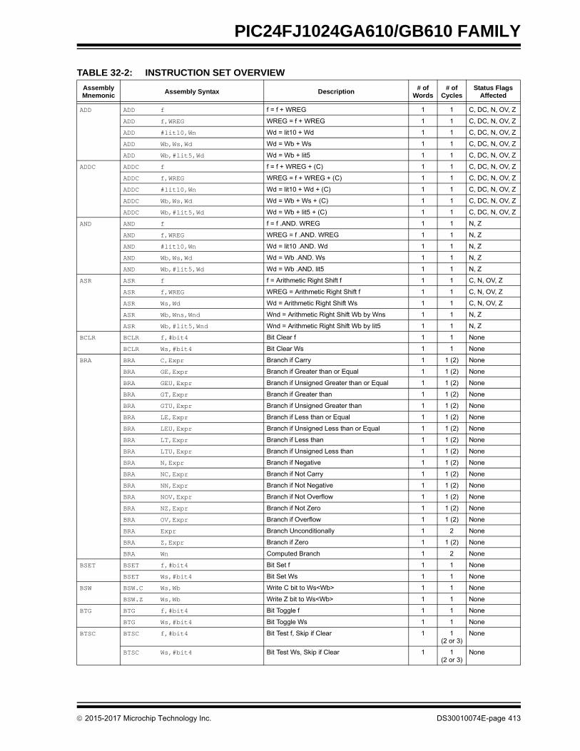
PIC24FJ1024GA610/GB610 FAMILY
TABLE 32-2: INSTRUCTION SET OVERVIEW
AssemblyMnemonic
Assembly Syntax Description# of
Words# of
CyclesStatus Flags
Affected
ADD ADD f f = f + WREG 1 1 C, DC, N, OV, Z
ADD f,WREG WREG = f + WREG 1 1 C, DC, N, OV, Z
ADD #lit10,Wn Wd = lit10 + Wd 1 1 C, DC, N, OV, Z
ADD Wb,Ws,Wd Wd = Wb + Ws 1 1 C, DC, N, OV, Z
ADD Wb,#lit5,Wd Wd = Wb + lit5 1 1 C, DC, N, OV, Z
ADDC ADDC f f = f + WREG + (C) 1 1 C, DC, N, OV, Z
ADDC f,WREG WREG = f + WREG + (C) 1 1 C, DC, N, OV, Z
ADDC #lit10,Wn Wd = lit10 + Wd + (C) 1 1 C, DC, N, OV, Z
ADDC Wb,Ws,Wd Wd = Wb + Ws + (C) 1 1 C, DC, N, OV, Z
ADDC Wb,#lit5,Wd Wd = Wb + lit5 + (C) 1 1 C, DC, N, OV, Z
AND AND f f = f .AND. WREG 1 1 N, Z
AND f,WREG WREG = f .AND. WREG 1 1 N, Z
AND #lit10,Wn Wd = lit10 .AND. Wd 1 1 N, Z
AND Wb,Ws,Wd Wd = Wb .AND. Ws 1 1 N, Z
AND Wb,#lit5,Wd Wd = Wb .AND. lit5 1 1 N, Z
ASR ASR f f = Arithmetic Right Shift f 1 1 C, N, OV, Z
ASR f,WREG WREG = Arithmetic Right Shift f 1 1 C, N, OV, Z
ASR Ws,Wd Wd = Arithmetic Right Shift Ws 1 1 C, N, OV, Z
ASR Wb,Wns,Wnd Wnd = Arithmetic Right Shift Wb by Wns 1 1 N, Z
ASR Wb,#lit5,Wnd Wnd = Arithmetic Right Shift Wb by lit5 1 1 N, Z
BCLR BCLR f,#bit4 Bit Clear f 1 1 None
BCLR Ws,#bit4 Bit Clear Ws 1 1 None
BRA BRA C,Expr Branch if Carry 1 1 (2) None
BRA GE,Expr Branch if Greater than or Equal 1 1 (2) None
BRA GEU,Expr Branch if Unsigned Greater than or Equal 1 1 (2) None
BRA GT,Expr Branch if Greater than 1 1 (2) None
BRA GTU,Expr Branch if Unsigned Greater than 1 1 (2) None
BRA LE,Expr Branch if Less than or Equal 1 1 (2) None
BRA LEU,Expr Branch if Unsigned Less than or Equal 1 1 (2) None
BRA LT,Expr Branch if Less than 1 1 (2) None
BRA LTU,Expr Branch if Unsigned Less than 1 1 (2) None
BRA N,Expr Branch if Negative 1 1 (2) None
BRA NC,Expr Branch if Not Carry 1 1 (2) None
BRA NN,Expr Branch if Not Negative 1 1 (2) None
BRA NOV,Expr Branch if Not Overflow 1 1 (2) None
BRA NZ,Expr Branch if Not Zero 1 1 (2) None
BRA OV,Expr Branch if Overflow 1 1 (2) None
BRA Expr Branch Unconditionally 1 2 None
BRA Z,Expr Branch if Zero 1 1 (2) None
BRA Wn Computed Branch 1 2 None
BSET BSET f,#bit4 Bit Set f 1 1 None
BSET Ws,#bit4 Bit Set Ws 1 1 None
BSW BSW.C Ws,Wb Write C bit to Ws<Wb> 1 1 None
BSW.Z Ws,Wb Write Z bit to Ws<Wb> 1 1 None
BTG BTG f,#bit4 Bit Toggle f 1 1 None
BTG Ws,#bit4 Bit Toggle Ws 1 1 None
BTSC BTSC f,#bit4 Bit Test f, Skip if Clear 1 1 (2 or 3)
None
BTSC Ws,#bit4 Bit Test Ws, Skip if Clear 1 1 (2 or 3)
None
2015-2017 Microchip Technology Inc. DS30010074E-page 413

PIC24FJ1024GA610/GB610 FAMILY
BTSS BTSS f,#bit4 Bit Test f, Skip if Set 1 1 (2 or 3)
None
BTSS Ws,#bit4 Bit Test Ws, Skip if Set 1 1 (2 or 3)
None
BTST BTST f,#bit4 Bit Test f 1 1 Z
BTST.C Ws,#bit4 Bit Test Ws to C 1 1 C
BTST.Z Ws,#bit4 Bit Test Ws to Z 1 1 Z
BTST.C Ws,Wb Bit Test Ws<Wb> to C 1 1 C
BTST.Z Ws,Wb Bit Test Ws<Wb> to Z 1 1 Z
BTSTS BTSTS f,#bit4 Bit Test then Set f 1 1 Z
BTSTS.C Ws,#bit4 Bit Test Ws to C, then Set 1 1 C
BTSTS.Z Ws,#bit4 Bit Test Ws to Z, then Set 1 1 Z
CALL CALL lit23 Call Subroutine 2 2 None
CALL Wn Call Indirect Subroutine 1 2 None
CLR CLR f f = 0x0000 1 1 None
CLR WREG WREG = 0x0000 1 1 None
CLR Ws Ws = 0x0000 1 1 None
CLRWDT CLRWDT Clear Watchdog Timer 1 1 WDTO, Sleep
COM COM f f = f 1 1 N, Z
COM f,WREG WREG = f 1 1 N, Z
COM Ws,Wd Wd = Ws 1 1 N, Z
CP CP f Compare f with WREG 1 1 C, DC, N, OV, Z
CP Wb,#lit5 Compare Wb with lit5 1 1 C, DC, N, OV, Z
CP Wb,Ws Compare Wb with Ws (Wb – Ws) 1 1 C, DC, N, OV, Z
CP0 CP0 f Compare f with 0x0000 1 1 C, DC, N, OV, Z
CP0 Ws Compare Ws with 0x0000 1 1 C, DC, N, OV, Z
CPB CPB f Compare f with WREG, with Borrow 1 1 C, DC, N, OV, Z
CPB Wb,#lit5 Compare Wb with lit5, with Borrow 1 1 C, DC, N, OV, Z
CPB Wb,Ws Compare Wb with Ws, with Borrow (Wb – Ws – C)
1 1 C, DC, N, OV, Z
CPSEQ CPSEQ Wb,Wn Compare Wb with Wn, Skip if = 1 1 (2 or 3)
None
CPSGT CPSGT Wb,Wn Compare Wb with Wn, Skip if > 1 1 (2 or 3)
None
CPSLT CPSLT Wb,Wn Compare Wb with Wn, Skip if < 1 1 (2 or 3)
None
CPSNE CPSNE Wb,Wn Compare Wb with Wn, Skip if 1 1 (2 or 3)
None
DAW DAW.B Wn Wn = Decimal Adjust Wn 1 1 C
DEC DEC f f = f –1 1 1 C, DC, N, OV, Z
DEC f,WREG WREG = f –1 1 1 C, DC, N, OV, Z
DEC Ws,Wd Wd = Ws – 1 1 1 C, DC, N, OV, Z
DEC2 DEC2 f f = f – 2 1 1 C, DC, N, OV, Z
DEC2 f,WREG WREG = f – 2 1 1 C, DC, N, OV, Z
DEC2 Ws,Wd Wd = Ws – 2 1 1 C, DC, N, OV, Z
DISI DISI #lit14 Disable Interrupts for k Instruction Cycles 1 1 None
DIV DIV.SW Wm,Wn Signed 16/16-bit Integer Divide 1 18 N, Z, C, OV
DIV.SD Wm,Wn Signed 32/16-bit Integer Divide 1 18 N, Z, C, OV
DIV.UW Wm,Wn Unsigned 16/16-bit Integer Divide 1 18 N, Z, C, OV
DIV.UD Wm,Wn Unsigned 32/16-bit Integer Divide 1 18 N, Z, C, OV
EXCH EXCH Wns,Wnd Swap Wns with Wnd 1 1 None
FF1L FF1L Ws,Wnd Find First One from Left (MSb) Side 1 1 C
FF1R FF1R Ws,Wnd Find First One from Right (LSb) Side 1 1 C
TABLE 32-2: INSTRUCTION SET OVERVIEW (CONTINUED)
AssemblyMnemonic
Assembly Syntax Description# of
Words# of
CyclesStatus Flags
Affected
DS30010074E-page 414 2015-2017 Microchip Technology Inc.

PIC24FJ1024GA610/GB610 FAMILY
GOTO GOTO Expr Go to Address 2 2 None
GOTO Wn Go to Indirect 1 2 None
INC INC f f = f + 1 1 1 C, DC, N, OV, Z
INC f,WREG WREG = f + 1 1 1 C, DC, N, OV, Z
INC Ws,Wd Wd = Ws + 1 1 1 C, DC, N, OV, Z
INC2 INC2 f f = f + 2 1 1 C, DC, N, OV, Z
INC2 f,WREG WREG = f + 2 1 1 C, DC, N, OV, Z
INC2 Ws,Wd Wd = Ws + 2 1 1 C, DC, N, OV, Z
IOR IOR f f = f .IOR. WREG 1 1 N, Z
IOR f,WREG WREG = f .IOR. WREG 1 1 N, Z
IOR #lit10,Wn Wd = lit10 .IOR. Wd 1 1 N, Z
IOR Wb,Ws,Wd Wd = Wb .IOR. Ws 1 1 N, Z
IOR Wb,#lit5,Wd Wd = Wb .IOR. lit5 1 1 N, Z
LNK LNK #lit14 Link Frame Pointer 1 1 None
LSR LSR f f = Logical Right Shift f 1 1 C, N, OV, Z
LSR f,WREG WREG = Logical Right Shift f 1 1 C, N, OV, Z
LSR Ws,Wd Wd = Logical Right Shift Ws 1 1 C, N, OV, Z
LSR Wb,Wns,Wnd Wnd = Logical Right Shift Wb by Wns 1 1 N, Z
LSR Wb,#lit5,Wnd Wnd = Logical Right Shift Wb by lit5 1 1 N, Z
MOV MOV f,Wn Move f to Wn 1 1 None
MOV [Wns+Slit10],Wnd Move [Wns+Slit10] to Wnd 1 1 None
MOV f Move f to f 1 1 N, Z
MOV f,WREG Move f to WREG 1 1 N, Z
MOV #lit16,Wn Move 16-bit Literal to Wn 1 1 None
MOV.b #lit8,Wn Move 8-bit Literal to Wn 1 1 None
MOV Wn,f Move Wn to f 1 1 None
MOV Wns,[Wns+Slit10] Move Wns to [Wns+Slit10] 1 1 None
MOV Wso,Wdo Move Ws to Wd 1 1 None
MOV WREG,f Move WREG to f 1 1 N, Z
MOV.D Wns,Wd Move Double from W(ns):W(ns+1) to Wd 1 2 None
MOV.D Ws,Wnd Move Double from Ws to W(nd+1):W(nd) 1 2 None
MUL MUL.SS Wb,Ws,Wnd Wnd+1, Wnd = Signed(Wb) * Signed(Ws) 1 1 None
MUL.SU Wb,Ws,Wnd Wnd+1, Wnd = Signed(Wb) * Unsigned(Ws) 1 1 None
MUL.US Wb,Ws,Wnd Wnd+1, Wnd = Unsigned(Wb) * Signed(Ws) 1 1 None
MUL.UU Wb,Ws,Wnd Wnd+1, Wnd = Unsigned(Wb) * Unsigned(Ws) 1 1 None
MUL.SU Wb,#lit5,Wnd Wnd+1, Wnd = Signed(Wb) * Unsigned(lit5) 1 1 None
MUL.UU Wb,#lit5,Wnd Wnd+1, Wnd = Unsigned(Wb) * Unsigned(lit5) 1 1 None
MUL f W3:W2 = f * WREG 1 1 None
NEG NEG f f = f + 1 1 1 C, DC, N, OV, Z
NEG f,WREG WREG = f + 1 1 1 C, DC, N, OV, Z
NEG Ws,Wd Wd = Ws + 1 1 1 C, DC, N, OV, Z
NOP NOP No Operation 1 1 None
NOPR No Operation 1 1 None
POP POP f Pop f from Top-of-Stack (TOS) 1 1 None
POP Wdo Pop from Top-of-Stack (TOS) to Wdo 1 1 None
POP.D Wnd Pop from Top-of-Stack (TOS) to W(nd):W(nd+1) 1 2 None
POP.S Pop Shadow Registers 1 1 All
PUSH PUSH f Push f to Top-of-Stack (TOS) 1 1 None
PUSH Wso Push Wso to Top-of-Stack (TOS) 1 1 None
PUSH.D Wns Push W(ns):W(ns+1) to Top-of-Stack (TOS) 1 2 None
PUSH.S Push Shadow Registers 1 1 None
TABLE 32-2: INSTRUCTION SET OVERVIEW (CONTINUED)
AssemblyMnemonic
Assembly Syntax Description# of
Words# of
CyclesStatus Flags
Affected
2015-2017 Microchip Technology Inc. DS30010074E-page 415

PIC24FJ1024GA610/GB610 FAMILY
PWRSAV PWRSAV #lit1 Go into Sleep or Idle mode 1 1 WDTO, Sleep
RCALL RCALL Expr Relative Call 1 2 None
RCALL Wn Computed Call 1 2 None
REPEAT REPEAT #lit14 Repeat Next Instruction lit14 + 1 times 1 1 None
REPEAT Wn Repeat Next Instruction (Wn) + 1 times 1 1 None
RESET RESET Software Device Reset 1 1 None
RETFIE RETFIE Return from Interrupt 1 3 (2) None
RETLW RETLW #lit10,Wn Return with Literal in Wn 1 3 (2) None
RETURN RETURN Return from Subroutine 1 3 (2) None
RLC RLC f f = Rotate Left through Carry f 1 1 C, N, Z
RLC f,WREG WREG = Rotate Left through Carry f 1 1 C, N, Z
RLC Ws,Wd Wd = Rotate Left through Carry Ws 1 1 C, N, Z
RLNC RLNC f f = Rotate Left (No Carry) f 1 1 N, Z
RLNC f,WREG WREG = Rotate Left (No Carry) f 1 1 N, Z
RLNC Ws,Wd Wd = Rotate Left (No Carry) Ws 1 1 N, Z
RRC RRC f f = Rotate Right through Carry f 1 1 C, N, Z
RRC f,WREG WREG = Rotate Right through Carry f 1 1 C, N, Z
RRC Ws,Wd Wd = Rotate Right through Carry Ws 1 1 C, N, Z
RRNC RRNC f f = Rotate Right (No Carry) f 1 1 N, Z
RRNC f,WREG WREG = Rotate Right (No Carry) f 1 1 N, Z
RRNC Ws,Wd Wd = Rotate Right (No Carry) Ws 1 1 N, Z
SE SE Ws,Wnd Wnd = Sign-Extended Ws 1 1 C, N, Z
SETM SETM f f = FFFFh 1 1 None
SETM WREG WREG = FFFFh 1 1 None
SETM Ws Ws = FFFFh 1 1 None
SL SL f f = Left Shift f 1 1 C, N, OV, Z
SL f,WREG WREG = Left Shift f 1 1 C, N, OV, Z
SL Ws,Wd Wd = Left Shift Ws 1 1 C, N, OV, Z
SL Wb,Wns,Wnd Wnd = Left Shift Wb by Wns 1 1 N, Z
SL Wb,#lit5,Wnd Wnd = Left Shift Wb by lit5 1 1 N, Z
SUB SUB f f = f – WREG 1 1 C, DC, N, OV, Z
SUB f,WREG WREG = f – WREG 1 1 C, DC, N, OV, Z
SUB #lit10,Wn Wn = Wn – lit10 1 1 C, DC, N, OV, Z
SUB Wb,Ws,Wd Wd = Wb – Ws 1 1 C, DC, N, OV, Z
SUB Wb,#lit5,Wd Wd = Wb – lit5 1 1 C, DC, N, OV, Z
SUBB SUBB f f = f – WREG – (C) 1 1 C, DC, N, OV, Z
SUBB f,WREG WREG = f – WREG – (C) 1 1 C, DC, N, OV, Z
SUBB #lit10,Wn Wn = Wn – lit10 – (C) 1 1 C, DC, N, OV, Z
SUBB Wb,Ws,Wd Wd = Wb – Ws – (C) 1 1 C, DC, N, OV, Z
SUBB Wb,#lit5,Wd Wd = Wb – lit5 – (C) 1 1 C, DC, N, OV, Z
SUBR SUBR f f = WREG – f 1 1 C, DC, N, OV, Z
SUBR f,WREG WREG = WREG – f 1 1 C, DC, N, OV, Z
SUBR Wb,Ws,Wd Wd = Ws – Wb 1 1 C, DC, N, OV, Z
SUBR Wb,#lit5,Wd Wd = lit5 – Wb 1 1 C, DC, N, OV, Z
SUBBR SUBBR f f = WREG – f – (C) 1 1 C, DC, N, OV, Z
SUBBR f,WREG WREG = WREG – f – (C) 1 1 C, DC, N, OV, Z
SUBBR Wb,Ws,Wd Wd = Ws – Wb – (C) 1 1 C, DC, N, OV, Z
SUBBR Wb,#lit5,Wd Wd = lit5 – Wb – (C) 1 1 C, DC, N, OV, Z
SWAP SWAP.b Wn Wn = Nibble Swap Wn 1 1 None
SWAP Wn Wn = Byte Swap Wn 1 1 None
TABLE 32-2: INSTRUCTION SET OVERVIEW (CONTINUED)
AssemblyMnemonic
Assembly Syntax Description# of
Words# of
CyclesStatus Flags
Affected
DS30010074E-page 416 2015-2017 Microchip Technology Inc.

PIC24FJ1024GA610/GB610 FAMILY
TBLRDH TBLRDH Ws,Wd Read Prog<23:16> to Wd<7:0> 1 2 None
TBLRDL TBLRDL Ws,Wd Read Prog<15:0> to Wd 1 2 None
TBLWTH TBLWTH Ws,Wd Write Ws<7:0> to Prog<23:16> 1 2 None
TBLWTL TBLWTL Ws,Wd Write Ws to Prog<15:0> 1 2 None
ULNK ULNK Unlink Frame Pointer 1 1 None
XOR XOR f f = f .XOR. WREG 1 1 N, Z
XOR f,WREG WREG = f .XOR. WREG 1 1 N, Z
XOR #lit10,Wn Wd = lit10 .XOR. Wd 1 1 N, Z
XOR Wb,Ws,Wd Wd = Wb .XOR. Ws 1 1 N, Z
XOR Wb,#lit5,Wd Wd = Wb .XOR. lit5 1 1 N, Z
ZE ZE Ws,Wnd Wnd = Zero-Extend Ws 1 1 C, Z, N
TABLE 32-2: INSTRUCTION SET OVERVIEW (CONTINUED)
AssemblyMnemonic
Assembly Syntax Description# of
Words# of
CyclesStatus Flags
Affected
2015-2017 Microchip Technology Inc. DS30010074E-page 417

PIC24FJ1024GA610/GB610 FAMILY
NOTES:
DS30010074E-page 418 2015-2017 Microchip Technology Inc.

PIC24FJ1024GA610/GB610 FAMILY
33.0 ELECTRICAL CHARACTERISTICS
This section provides an overview of the PIC24FJ1024GA610/GB610 family electrical characteristics. Additionalinformation will be provided in future revisions of this document as it becomes available.
Absolute maximum ratings for the PIC24FJ1024GA610/GB610 family are listed below. Exposure to these maximumrating conditions for extended periods may affect device reliability. Functional operation of the device at these, or anyother conditions above the parameters indicated in the operation listings of this specification, is not implied.
Absolute Maximum Ratings(†)
Ambient temperature under bias.............................................................................................................. .-40°C to +85°C
Storage temperature .............................................................................................................................. -65°C to +150°C
Voltage on VDD with respect to VSS ......................................................................................................... -0.3V to +4.0V
Voltage on any general purpose digital or analog pin (not 5.5V tolerant) with respect to VSS ....... -0.3V to (VDD + 0.3V)
Voltage on any general purpose digital or analog pin (5.5V tolerant, including MCLR) with respect to VSS:
When VDD = 0V: .......................................................................................................................... -0.3V to +4.0V
When VDD 2.0V: ....................................................................................................................... -0.3V to +6.0V
Voltage on AVDD with respect to VSS ................................................... (VDD – 0.3V) to (lesser of: 4.0V or (VDD + 0.3V))
Voltage on AVSS with respect to VSS ........................................................................................................ -0.3V to +0.3V
Maximum current out of VSS pin ...........................................................................................................................300 mA
Maximum current into VDD pin (Note 1)................................................................................................................250 mA
Maximum output current sunk by any I/O pin .........................................................................................................25 mA
Maximum output current sourced by any I/O pin ....................................................................................................25 mA
Maximum current sunk by all ports .......................................................................................................................200 mA
Maximum current sourced by all ports (Note 1)....................................................................................................200 mA
Note 1: Maximum allowable current is a function of device maximum power dissipation (see Table 33-1).
† NOTICE: Stresses above those listed under “Absolute Maximum Ratings” may cause permanent damage to the device. This is a stress rating only and functional operation of the device at those or any other conditions above those indicated in the operation listings of this specification is not implied. Exposure to maximum rating conditions for extended periods may affect device reliability.
2015-2017 Microchip Technology Inc. DS30010074E-page 419
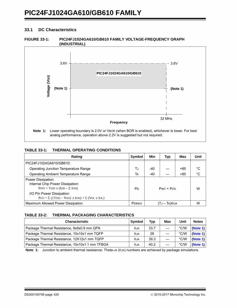
PIC24FJ1024GA610/GB610 FAMILY
33.1 DC Characteristics
FIGURE 33-1: PIC24FJ1024GA610/GB610 FAMILY VOLTAGE-FREQUENCY GRAPH (INDUSTRIAL)
TABLE 33-1: THERMAL OPERATING CONDITIONS
Rating Symbol Min Typ Max Unit
PIC24FJ1024GA610/GB610:
Operating Junction Temperature Range TJ -40 — +85 °C
Operating Ambient Temperature Range TA -40 — +85 °C
Power Dissipation: Internal Chip Power Dissipation:
PINT = VDD x (IDD – IOH) PD PINT + PI/O W I/O Pin Power Dissipation:
PI/O = (VDD – VOH x IOH) + (VOL x IOL)
Maximum Allowed Power Dissipation PDMAX (TJ – TA)/JA W
Frequency
Vo
ltag
e (
VD
D)
(Note 1)
32 MHz
3.6V 3.6V
(Note 1)
Note 1: Lower operating boundary is 2.0V or VBOR (when BOR is enabled), whichever is lower. For best analog performance, operation above 2.2V is suggested but not required.
PIC24FJ1024GA610/GB610
TABLE 33-2: THERMAL PACKAGING CHARACTERISTICS
Characteristic Symbol Typ Max Unit Notes
Package Thermal Resistance, 9x9x0.9 mm QFN JA 33.7 — °C/W (Note 1)
Package Thermal Resistance, 10x10x1 mm TQFP JA 28 — °C/W (Note 1)
Package Thermal Resistance, 12X12x1 mm TQFP JA 39.3 — °C/W (Note 1)
Package Thermal Resistance, 10x10x1.1 mm TFBGA JA 40.2 — °C/W (Note 1)
Note 1: Junction to ambient thermal resistance; Theta-JA (JA) numbers are achieved by package simulations.
DS30010074E-page 420 2015-2017 Microchip Technology Inc.
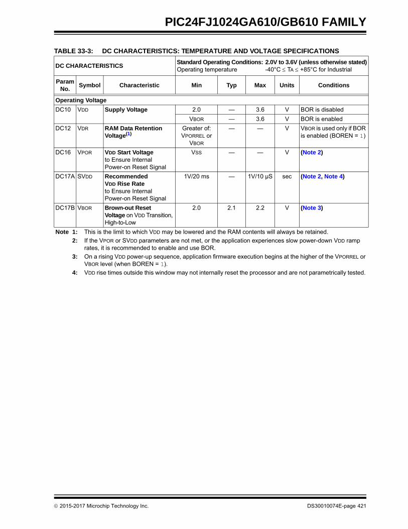
PIC24FJ1024GA610/GB610 FAMILY
TABLE 33-3: DC CHARACTERISTICS: TEMPERATURE AND VOLTAGE SPECIFICATIONS
DC CHARACTERISTICSStandard Operating Conditions: 2.0V to 3.6V (unless otherwise stated)Operating temperature -40°C TA +85°C for Industrial
Param No.
Symbol Characteristic Min Typ Max Units Conditions
Operating Voltage
DC10 VDD Supply Voltage 2.0 — 3.6 V BOR is disabled
VBOR — 3.6 V BOR is enabled
DC12 VDR RAM Data Retention Voltage(1)
Greater of:VPORREL or
VBOR
— — V VBOR is used only if BOR is enabled (BOREN = 1)
DC16 VPOR VDD Start Voltageto Ensure InternalPower-on Reset Signal
VSS — — V (Note 2)
DC17A SVDD RecommendedVDD Rise Rateto Ensure InternalPower-on Reset Signal
1V/20 ms — 1V/10 µS sec (Note 2, Note 4)
DC17B VBOR Brown-out Reset Voltage on VDD Transition, High-to-Low
2.0 2.1 2.2 V (Note 3)
Note 1: This is the limit to which VDD may be lowered and the RAM contents will always be retained.
2: If the VPOR or SVDD parameters are not met, or the application experiences slow power-down VDD ramp rates, it is recommended to enable and use BOR.
3: On a rising VDD power-up sequence, application firmware execution begins at the higher of the VPORREL or VBOR level (when BOREN = 1).
4: VDD rise times outside this window may not internally reset the processor and are not parametrically tested.
2015-2017 Microchip Technology Inc. DS30010074E-page 421

PIC24FJ1024GA610/GB610 FAMILY
TABLE 33-4: DC CHARACTERISTICS: OPERATING CURRENT (IDD)
DC CHARACTERISTICSStandard Operating Conditions: 2.0V to 3.6V (unless otherwise stated)Operating temperature -40°C TA +85°C for Industrial
Parameter No.
Typical(1) Max UnitsOperating
TemperatureVDD Conditions
Operating Current (IDD)(2)
DC19 230 365 A -40°C to +85°C 2.0V 0.5 MIPS,FOSC = 1 MHz250 365 A -40°C to +85°C 3.3V
DC20 430 640 A -40°C to +85°C 2.0V 1 MIPS,FOSC = 2 MHz440 640 A -40°C to +85°C 3.3V
DC23 1.5 2.4 mA -40°C to +85°C 2.0V 4 MIPS,FOSC = 8 MHz1.65 2.4 mA -40°C to +85°C 3.3V
DC24 6.1 7.7 mA -40°C to +85°C 2.0V 16 MIPS,FOSC = 32 MHz6.3 7.7 mA -40°C to +85°C 3.3V
DC31 43 130 A -40°C to +85°C 2.0V LPRC (15.5 KIPS),FOSC = 31 kHz46 130 A -40°C to +85°C 3.3V
DC32 1.63 2.5 mA -40°C to +85°C 2.0V FRC (4 MIPS),FOSC = 8 MHz1.65 2.5 mA -40°C to +85°C 3.3V
DC33 1.9 3.0 mA -40°C to +85°C 2.0V DCO (4 MIPS),FOSC = 8 MHz2.0 3.0 mA -40°C to +85°C 3.3V
Note 1: Data in the “Typical” column is at 3.3V, +25°C unless otherwise stated. Typical parameters are for design guidance only and are not tested.
2: The test conditions for all IDD measurements are as follows: OSC1 driven with external square wave from rail-to-rail. All I/O pins are configured as outputs driving low. MCLR = VDD; WDT and FSCM are disabled. CPU, program memory and data memory are operational. All peripheral modules are clocked but inactive (PMDx bits are all ‘1’). JTAG module is disabled.
TABLE 33-5: DC CHARACTERISTICS: IDLE CURRENT (IIDLE)
DC CHARACTERISTICSStandard Operating Conditions: 2.0V to 3.6V (unless otherwise stated)Operating temperature -40°C TA +85°C for Industrial
Parameter No.
Typical(1) Max UnitsOperating
TemperatureVDD Conditions
Idle Current (IIDLE)(2)
DC40 95 215 A -40°C to +85°C 2.0V 1 MIPS,FOSC = 2 MHz105 225 A -40°C to +85°C 3.3V
DC43 290 720 A -40°C to +85°C 2.0V 4 MIPS,FOSC = 8 MHz315 750 A -40°C to +85°C 3.3V
DC47 1.05 2.7 mA -40°C to +85°C 2.0V 16 MIPS,FOSC = 32 MHz1.16 2.8 mA -40°C to +85°C 3.3V
DC50 350 820 A -40°C to +85°C 2.0V FRC (4 MIPS),FOSC = 8 MHz360 850 A -40°C to +85°C 3.3V
DC51 26 110 A -40°C to +85°C 2.0V LPRC (15.5 KIPS),FOSC = 31 kHz30 110 A -40°C to +85°C 3.3V
Note 1: Data in the “Typical” column is at 3.3V, +25°C unless otherwise stated. Parameters are for design guidance only and are not tested.
2: Base IIDLE current is measured with the core off, the clock on and all modules turned off. Peripheral Module Disable SFR registers are ‘1’. All I/O pins are configured as outputs driving low. JTAG module is disabled.
DS30010074E-page 422 2015-2017 Microchip Technology Inc.

PIC24FJ1024GA610/GB610 FAMILY
TABLE 33-6: DC CHARACTERISTICS: POWER-DOWN CURRENT (IPD)
DC CHARACTERISTICSStandard Operating Conditions: 2.0V to 3.6V (unless otherwise stated)Operating temperature -40°C TA +85°C for Industrial
Parameter No.
Typical(1) Max UnitsOperating
TemperatureVDD Conditions
Power-Down Current(4,5)
DC60 2.5 10 A -40°C
2.0V
Sleep(2)
3.2 10 A +25°C
11.5 45 A +85°C
3.2 10 A -40°C
3.3V4.0 10 A +25°C
12.2 45 A +85°C
DC61 165 — nA -40°C
2.0V
Low-Voltage Retention Sleep(3)
190 — nA +25°C
14.5 — A +85°C
220 — nA -40°C
3.3V300 — nA +25°C
15 — A +85°C
Note 1: Data in the “Typical” column is at 3.3V, +25°C unless otherwise stated. Parameters are for design guidance only and are not tested.
2: The retention low-voltage regulator is disabled; RETEN (RCON<12>) = 0, LPCFG (FPOR<2>) = 1.3: The retention low-voltage regulator is enabled; RETEN (RCON<12>) = 1, LPCFG (FPOR<2>) = 0.
4: Base IPD is measured with all peripherals and clocks shut down. All I/Os are configured as outputs and driven low. WDT, etc., are all switched off.
5: These currents are measured on the device containing the most memory in this family.
2015-2017 Microchip Technology Inc. DS30010074E-page 423
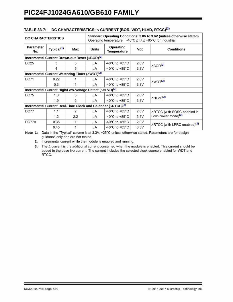
PIC24FJ1024GA610/GB610 FAMILY
TABLE 33-7: DC CHARACTERISTICS: CURRENT (BOR, WDT, HLVD, RTCC)(3)
DC CHARACTERISTICSStandard Operating Conditions: 2.0V to 3.6V (unless otherwise stated)Operating temperature -40°C TA +85°C for Industrial
Parameter No.
Typical(1) Max UnitsOperating
TemperatureVDD Conditions
Incremental Current Brown-out Reset (BOR)(2)
DC25 3 5 A -40°C to +85°C 2.0VBOR(2)
4 5 A -40°C to +85°C 3.3V
Incremental Current Watchdog Timer (WDT)(2)
DC71 0.22 1 A -40°C to +85°C 2.0VWDT(2)
0.3 1 A -40°C to +85°C 3.3V
Incremental Current High/Low-Voltage Detect (HLVD)(2)
DC75 1.3 5 A -40°C to +85°C 2.0VHLVD(2)
1.9 5 A -40°C to +85°C 3.3V
Incremental Current Real-Time Clock and Calendar (RTCC)(2)
DC77 1.1 2 A -40°C to +85°C 2.0V RTCC (with SOSC enabled in Low-Power mode)(2)
1.2 2.2 A -40°C to +85°C 3.3V
DC77A 0.35 1 A -40°C to +85°C 2.0VRTCC (with LPRC enabled)(2)
0.45 1 A -40°C to +85°C 3.3V
Note 1: Data in the “Typical” column is at 3.3V, +25°C unless otherwise stated. Parameters are for design guidance only and are not tested.
2: Incremental current while the module is enabled and running.
3: The current is the additional current consumed when the module is enabled. This current should be added to the base IPD current. The current includes the selected clock source enabled for WDT and RTCC.
DS30010074E-page 424 2015-2017 Microchip Technology Inc.

PIC24FJ1024GA610/GB610 FAMILY
TABLE 33-8: DC CHARACTERISTICS: I/O PIN INPUT SPECIFICATIONS
DC CHARACTERISTICSStandard Operating Conditions: 2.0V to 3.6V (unless otherwise stated)Operating temperature -40°C TA +85°C for Industrial
Param No.
Symbol Characteristic Min Typ(1) Max Units Conditions
VIL Input Low Voltage(3)
DI10 I/O Pins with ST Buffer VSS — 0.2 VDD V
DI11 I/O Pins with TTL Buffer VSS — 0.15 VDD V
DI15 MCLR VSS — 0.2 VDD V
DI16 OSCI (XT mode) VSS — 0.2 VDD V
DI17 OSCI (HS mode) VSS — 0.2 VDD V
DI18 I/O Pins with I2C Buffer VSS — 0.3 VDD V
DI19 I/O Pins with SMBus Buffer VSS — 0.8 V SMBus is enabled
VIH Input High Voltage(3)
DI20 I/O Pins with ST Buffer: with Analog Functions, Digital Only
0.8 VDD
0.8 VDD
——
VDD
5.5VV
DI21 I/O Pins with TTL Buffer: with Analog Functions, Digital Only
0.25 VDD + 0.80.25 VDD + 0.8
——
VDD
5.5VV
DI25 MCLR 0.8 VDD — VDD V
DI26 OSCI (XT mode) 0.7 VDD — VDD V
DI27 OSCI (HS mode) 0.7 VDD — VDD V
DI28 I/O Pins with I2C Buffer: with Analog Functions, Digital Only
0.7 VDD
0.7 VDD
——
VDD
5.5VV
DI29 I/O Pins with SMBus Buffer: with Analog Functions, Digital Only
2.12.1
——
VDD
5.5VV
2.5V VPIN VDD
DI30 ICNPU CNx Pull-up Current 150 450 A VDD = 3.3V, VPIN = VSS
DI30A ICNPD CNx Pull-Down Current 230 500 A VDD = 3.3V, VPIN = VDD
IIL Input Leakage Current(2)
DI50 I/O Ports — — ±1 A VSS VPIN VDD,pin at high-impedance
DI51 Analog Input Pins — — ±1 A VSS VPIN VDD,pin at high-impedance
DI55 MCLR — — ±1 A VSS VPIN VDD
DI56 OSCI/CLKI — — ±1 A VSS VPIN VDD, EC, XT and HS modes
Note 1: Data in the “Typ” column is at 3.3V, +25°C unless otherwise stated. Parameters are for design guidance only and are not tested.
2: Negative current is defined as current sourced by the pin.
3: Refer to Table 1-1 for I/O pin buffer types.
2015-2017 Microchip Technology Inc. DS30010074E-page 425

PIC24FJ1024GA610/GB610 FAMILY
TABLE 33-9: DC CHARACTERISTICS: I/O PIN OUTPUT SPECIFICATIONS
DC CHARACTERISTICSStandard Operating Conditions: 2.0V to 3.6V (unless otherwise stated)Operating temperature -40°C TA +85°C for Industrial
Param No.
Symbol Characteristic Min Typ(1) Max Units Conditions
VOL Output Low Voltage
DO10 I/O Ports — — 0.4 V IOL = 6.6 mA, VDD = 3.6V
— — 0.8 V IOL = 18 mA, VDD = 3.6V
— — 0.35 V IOL = 5.0 mA, VDD = 2V
DO16 OSCO/CLKO — — 0.18 V IOL = 6.6 mA, VDD = 3.6V
— — 0.2 V IOL = 5.0 mA, VDD = 2V
VOH Output High Voltage
DO20 I/O Ports 3.4 — — V IOH = -3.0 mA, VDD = 3.6V
3.25 — — V IOH = -6.0 mA, VDD = 3.6V
2.8 — — V IOH = -18 mA, VDD = 3.6V
1.65 — — V IOH = -1.0 mA, VDD = 2V
1.4 — — V IOH = -3.0 mA, VDD = 2V
DO26 OSCO/CLKO 3.3 — — V IOH = -6.0 mA, VDD = 3.6V
1.85 — — V IOH = -1.0 mA, VDD = 2V
Note 1: Data in the “Typ” column is at 3.3V, +25°C unless otherwise stated. Parameters are for design guidance only and are not tested.
TABLE 33-10: DC CHARACTERISTICS: PROGRAM MEMORY
DC CHARACTERISTICSStandard Operating Conditions: 2.0V to 3.6V (unless otherwise stated)Operating temperature -40°C TA +85°C for Industrial
ParamNo.
Symbol Characteristic Min Typ(1) Max Units Conditions
Program Flash Memory
D130 EP Cell Endurance 10000 — — E/W -40C to +85C
D131 VPR VDD for Read VMIN — 3.6 V VMIN = Minimum operating voltage
D132B VDD for Self-Timed Write VMIN — 3.6 V VMIN = Minimum operating voltage
D133A TIW Self-Timed Word Write Cycle Time
— 20 — s
Self-Timed Row Write Cycle Time
— 1.5 — ms
D133B TIE Self-Timed Page Erase Time
20 — 40 ms
D134 TRETD Characteristic Retention 20 — — Year If no other specifications are violated
D135 IDDP Supply Current during Programming
— 5 — mA
Note 1: Data in the “Typ” column is at 3.3V, +25°C unless otherwise stated.
DS30010074E-page 426 2015-2017 Microchip Technology Inc.

PIC24FJ1024GA610/GB610 FAMILY
TABLE 33-11: INTERNAL VOLTAGE REGULATOR SPECIFICATIONS
TABLE 33-12: HIGH/LOW-VOLTAGE DETECT CHARACTERISTICS
Operating Conditions: -40°C < TA < +85°C (unless otherwise stated)
ParamNo.
Symbol Characteristics Min Typ Max Units Comments
DVR TVREG Voltage Regulator Start-up Time — 10 — s VREGS = 0 with any POR or BOR
DVR10 VBG Internal Band Gap Reference 1.14 1.2 1.26 V
DVR11 TBG Band Gap Reference Start-up Time
— 1 — ms
DVR20 VRGOUT Regulator Output Voltage 1.6 1.8 2 V VDD > 2.1V
DVR21 CEFC External Filter Capacitor Value 10 — — F Series resistance < 3recommended; < 5 required
DVR30 VLVR Low-Voltage Regulator Output Voltage
— 1.2 — V RETEN = 1, LPCFG = 0
Operating Conditions: -40°C < TA < +85°C (unless otherwise stated)
Param No.
Symbol Characteristic Min Typ Max Units Conditions
DC18 VHLVD HLVD Voltage on VDD Transition
HLVDL<3:0> = 0100(1) 3.40 — 3.74 V
VDIR = 1
HLVDL<3:0> = 0101 3.25 — 3.58 V
HLVDL<3:0> = 0110 2.95 — 3.25 V
HLVDL<3:0> = 0111 2.75 — 3.04 V
HLVDL<3:0> = 1000 2.65 — 2.93 V
HLVDL<3:0> = 1001 2.45 — 2.75 V
HLVDL<3:0> = 1010 2.35 — 2.64 V
HLVDL<3:0> = 1011 2.25 — 2.50 V
HLVDL<3:0> = 1100 2.15 — 2.39 V
HLVDL<3:0> = 1101 2.08 — 2.28 V
HLVDL<3:0> = 1110 2.00 — 2.17 V
DC101 VTHL HLVD Voltage on HLVDIN Pin Transition
HLVDL<3:0> = 1111 — 1.20 — V
DC105 TONLVD HLVD Module Enable Time — 5 — µS From POR or HLVDEN = 1
Note 1: Trip points for values of HLVD<3:0>, from ‘0000’ to ‘0011’, are not implemented.
2015-2017 Microchip Technology Inc. DS30010074E-page 427
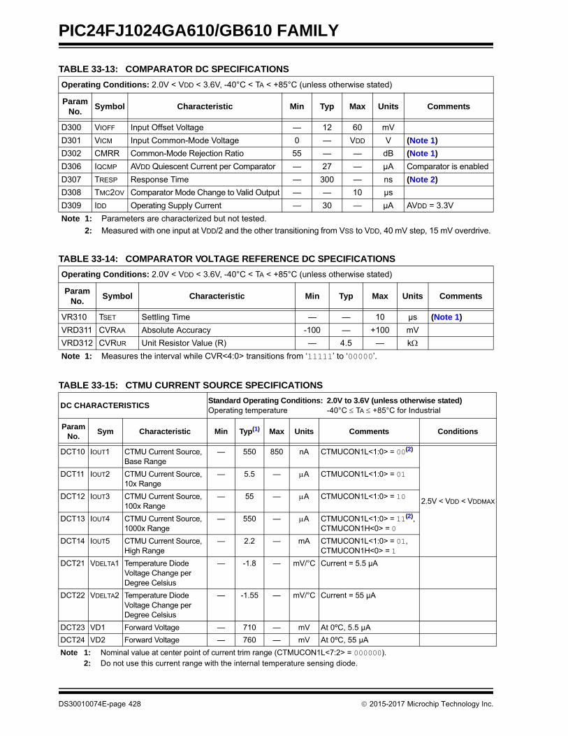
PIC24FJ1024GA610/GB610 FAMILY
TABLE 33-13: COMPARATOR DC SPECIFICATIONS
TABLE 33-14: COMPARATOR VOLTAGE REFERENCE DC SPECIFICATIONS
Operating Conditions: 2.0V < VDD < 3.6V, -40°C < TA < +85°C (unless otherwise stated)
ParamNo.
Symbol Characteristic Min Typ Max Units Comments
D300 VIOFF Input Offset Voltage — 12 60 mV
D301 VICM Input Common-Mode Voltage 0 — VDD V (Note 1)
D302 CMRR Common-Mode Rejection Ratio 55 — — dB (Note 1)
D306 IQCMP AVDD Quiescent Current per Comparator — 27 — µA Comparator is enabled
D307 TRESP Response Time — 300 — ns (Note 2)
D308 TMC2OV Comparator Mode Change to Valid Output — — 10 µs
D309 IDD Operating Supply Current — 30 — µA AVDD = 3.3V
Note 1: Parameters are characterized but not tested.
2: Measured with one input at VDD/2 and the other transitioning from VSS to VDD, 40 mV step, 15 mV overdrive.
Operating Conditions: 2.0V < VDD < 3.6V, -40°C < TA < +85°C (unless otherwise stated)
ParamNo.
Symbol Characteristic Min Typ Max Units Comments
VR310 TSET Settling Time — — 10 µs (Note 1)
VRD311 CVRAA Absolute Accuracy -100 — +100 mV
VRD312 CVRUR Unit Resistor Value (R) — 4.5 — k
Note 1: Measures the interval while CVR<4:0> transitions from ‘11111’ to ‘00000’.
TABLE 33-15: CTMU CURRENT SOURCE SPECIFICATIONS
DC CHARACTERISTICSStandard Operating Conditions: 2.0V to 3.6V (unless otherwise stated)Operating temperature -40°C TA +85°C for Industrial
ParamNo.
Sym Characteristic Min Typ(1) Max Units Comments Conditions
DCT10 IOUT1 CTMU Current Source, Base Range
— 550 850 nA CTMUCON1L<1:0> = 00(2)
2.5V < VDD < VDDMAX
DCT11 IOUT2 CTMU Current Source, 10x Range
— 5.5 — A CTMUCON1L<1:0> = 01
DCT12 IOUT3 CTMU Current Source, 100x Range
— 55 — A CTMUCON1L<1:0> = 10
DCT13 IOUT4 CTMU Current Source, 1000x Range
— 550 — A CTMUCON1L<1:0> = 11(2), CTMUCON1H<0> = 0
DCT14 IOUT5 CTMU Current Source, High Range
— 2.2 — mA CTMUCON1L<1:0> = 01, CTMUCON1H<0> = 1
DCT21 VDELTA1 Temperature Diode Voltage Change per Degree Celsius
— -1.8 — mV/°C Current = 5.5 µA
DCT22 VDELTA2 Temperature Diode Voltage Change per Degree Celsius
— -1.55 — mV/°C Current = 55 µA
DCT23 VD1 Forward Voltage — 710 — mV At 0ºC, 5.5 µA
DCT24 VD2 Forward Voltage — 760 — mV At 0ºC, 55 µA
Note 1: Nominal value at center point of current trim range (CTMUCON1L<7:2> = 000000).2: Do not use this current range with the internal temperature sensing diode.
DS30010074E-page 428 2015-2017 Microchip Technology Inc.

PIC24FJ1024GA610/GB610 FAMILY
33.2 AC Characteristics and Timing Parameters
The information contained in this section defines the PIC24FJ1024GA610/GB610 family AC characteristics and timingparameters.
TABLE 33-16: TEMPERATURE AND VOLTAGE SPECIFICATIONS – AC
FIGURE 33-2: LOAD CONDITIONS FOR DEVICE TIMING SPECIFICATIONS
TABLE 33-17: CAPACITIVE LOADING REQUIREMENTS ON OUTPUT PINS
AC CHARACTERISTICSStandard Operating Conditions: 2.0V to 3.6V (unless otherwise stated)Operating temperature -40°C TA +85°C for Industrial Operating voltage VDD range as described in Section 33.1 “DC Characteristics”.
Param No.
Symbol Characteristic Min Typ(1) Max Units Conditions
DO50 COSCO OSCO/CLKO Pin — — 15 pF In XT and HS modes when external clock is used to drive OSCI
DO56 CIO All I/O Pins and OSCO — — 50 pF EC mode
DO58 CB SCLx, SDAx — — 400 pF In I2C mode
Note 1: Data in the “Typ” column is at 3.3V, +25°C unless otherwise stated. Parameters are for design guidance only and are not tested.
VDD/2
CL
RL
Pin
Pin
VSS
VSS
CL
RL = 464CL = 50 pF for all pins except OSCO
15 pF for OSCO output
Load Condition 1 – for all pins except OSCO Load Condition 2 – for OSCO
2015-2017 Microchip Technology Inc. DS30010074E-page 429

PIC24FJ1024GA610/GB610 FAMILY
FIGURE 33-3: EXTERNAL CLOCK TIMING
TABLE 33-18: EXTERNAL CLOCK TIMING REQUIREMENTS
AC CHARACTERISTICSStandard Operating Conditions: 2.0V to 3.6V (unless otherwise stated)Operating temperature -40°C TA +85°C for Industrial
ParamNo.
Symbol Characteristic Min Typ(1) Max Units Conditions
OS10 FOSC External CLKI Frequency(External clocks allowed only in EC mode)
DC4
——
3248
MHzMHz
ECECPLL (Note 2)
Oscillator Frequency 3.54
101231
—————
108
322433
MHzMHzMHzMHzkHz
XTXTPLLHSHSPLLSOSC
OS20 TOSC TOSC = 1/FOSC — — — — See Parameter OS10 for FOSC value
OS25 TCY Instruction Cycle Time(3) 62.5 — DC ns
OS30 TosL,TosH
External Clock in (OSCI)High or Low Time
0.45 x TOSC — — ns EC
OS31 TosR,TosF
External Clock in (OSCI)Rise or Fall Time
— — 20 ns EC
OS40 TckR CLKO Rise Time(4) — 15 30 ns
OS41 TckF CLKO Fall Time(4) — 15 30 ns
Note 1: Data in the “Typ” column is at 3.3V, +25°C unless otherwise stated. Parameters are for design guidance only and are not tested.
2: Represents input to the system clock prescaler. PLL dividers and postscalers must still be configured so that the system clock frequency does not exceed the maximum frequency shown in Figure 33-1.
3: Instruction cycle period (TCY) equals two times the input oscillator time base period. All specified values are based on characterization data for that particular oscillator type, under standard operating conditions, with the device executing code. Exceeding these specified limits may result in an unstable oscillator operation and/or higher than expected current consumption. All devices are tested to operate at “Min.” values with an external clock applied to the OSCI/CLKI pin. When an external clock input is used, the “Max.” cycle time limit is “DC” (no clock) for all devices.
4: Measurements are taken in EC mode. The CLKO signal is measured on the OSCO pin. CLKO is low for the Q1-Q2 period (1/2 TCY) and high for the Q3-Q4 period (1/2 TCY).
OSCI
CLKO
Q4 Q1 Q2 Q3 Q4 Q1
OS20
OS25OS30 OS30
OS40 OS41
OS31OS31
Q1 Q2 Q3 Q4 Q2 Q3
DS30010074E-page 430 2015-2017 Microchip Technology Inc.

PIC24FJ1024GA610/GB610 FAMILY
TABLE 33-19: AC SPECIFICATIONS FOR PHASE-LOCKED LOOP MODE
AC CHARACTERISTICSStandard Operating Conditions: 2.0V to 3.6V (unless otherwise stated)Operating temperature -40°C TA +85°C for Industrial
Sym Characteristic Min Typ Max Units Conditions
FIN Input Frequency Range 2 — 24 MHz
FMIN Minimum Output Frequency from the Frequency Multiplier
— — 16 MHz 4 MHz FIN with 4x feedback ratio,2 MHz FIN with 8x feedback ratio
FMAX Maximum Output Frequency from the Frequency Multiplier
96 — — MHz 4 MHz FIN with 24x net multiplication ratio,24 MHz FIN with 4x net multiplication ratio
FSLEW Maximum Step Function of FIN at which the PLL will be Ensured to Maintain Lock
-4 — +4 % Full input range of FIN
TLOCK Lock Time for VCO — — 24 s With the specified minimum, TREF, and a lock timer count of one cycle, this is the maximum VCO lock time supported
JFM8 Cumulative Jitter of Frequency Multiplier Over Voltage and Temperature During Any Eight Consecutive Cycles of the PLL Output
— — ±0.12 % External 8 MHz crystal and 96 MHZ PLL mode
2015-2017 Microchip Technology Inc. DS30010074E-page 431

PIC24FJ1024GA610/GB610 FAMILY
TABLE 33-20: INTERNAL RC ACCURACY
AC CHARACTERISTICSStandard Operating Conditions: 2.0V to 3.6V (unless otherwise stated)Operating temperature -40°C TA +85°C for Industrial
Param No.
Characteristic Min Typ Max Units Conditions
F20 FRC Accuracy @ 8 MHz -1.5 +0.15 1.5 % 2.0V VDD 3.6V, 0°C TA +85°C (Note 1)
-2.0 — 2.0 % 2.0V VDD 3.6V, -40°C TA 0°C
-0.20 +0.05 -0.20 % 2.0V VDD 3.6V, 0°C TA +85°C, self-tune is enabled and locked (Note 2)
F21 LPRC @ 31 kHz -20 — 20 % VCAP Output Voltage = 1.8V
F22 OSCTUN Step-Size — 0.05 — %/bit
F23 FRC Self-Tune Lock Time — 5 8 ms (Note 3)
Note 1: To achieve this accuracy, physical stress applied to the microcontroller package (ex., by flexing the PCB) must be kept to a minimum.
2: Accuracy is measured with respect to the reference source.
3: Time from reference clock stable, and in range, to FRC tuned within range specified by F20 (with self-tune).
TABLE 33-21: RC OSCILLATOR START-UP TIME
AC CHARACTERISTICS Standard Operating Conditions: 2.0V to 3.6V (unless otherwise stated)Operating temperature -40°C TA +85°C for Industrial
ParamNo.
Symbol Characteristic Min Typ Max Units Conditions
FR0 TFRC FRC Oscillator Start-up Time
— 15 — s
FR1 TLPRC Low-Power RC Oscillator Start-up Time
— 50 — s
DS30010074E-page 432 2015-2017 Microchip Technology Inc.

PIC24FJ1024GA610/GB610 FAMILY
TABLE 33-22: INTERNAL DCO ACCURACY
AC CHARACTERISTICS Standard Operating Conditions: 2.0V to 3.6V (unless otherwise stated)Operating temperature -40°C TA +85°C for Industrial
ParamNo.
Symbol Characteristic Min Typ Max Units Conditions
F30 FDCO DCO Frequency 7.44 8.00 8.56 MHz
14.88 16.0 17.12 MHz
29.76 32.0 32.24 MHz
F31 DCOSU DCO Start-up Time — 1.0 2.0 s
F32 DCOSTABLE DCO Stabilization Period — 8 — Clocks
F33 DCODT DCO Temperature Drift — 0.4 — %/°C
F34 DCOVT DCO Voltage Drift — 0.2 — %/V
F35 DCODC DCO Duty Cycle 48 50 52 %
2015-2017 Microchip Technology Inc. DS30010074E-page 433

PIC24FJ1024GA610/GB610 FAMILY
FIGURE 33-4: CLKO AND I/O TIMING CHARACTERISTICS
TABLE 33-23: CLKO AND I/O TIMING REQUIREMENTS
AC CHARACTERISTICSStandard Operating Conditions: 2.0V to 3.6V (unless otherwise stated)Operating temperature -40°C TA +85°C for Industrial
ParamNo.
Symbol Characteristic Min Typ(1) Max Units Conditions
DO31 TIOR Port Output Rise Time — 10 25 ns
DO32 TIOF Port Output Fall Time — 10 25 ns
DI35 TINP INTx Pin High or Low Time (input)
1 — — TCY
DI40 TRBP CNx High or Low Time (input)
1 — — TCY
Note 1: Data in the “Typ” column is at 3.3V, +25°C unless otherwise stated.
Note: Refer to Figure 33-2 for load conditions.
I/O Pin(Input)
I/O Pin(Output)
DI35
Old Value New Value
DI40
DO31DO32
DS30010074E-page 434 2015-2017 Microchip Technology Inc.

PIC24FJ1024GA610/GB610 FAMILY
TABLE 33-24: RESET AND BROWN-OUT RESET REQUIREMENTS
AC CHARACTERISTICS Standard Operating Conditions: 2.0V to 3.6V (unless otherwise stated)Operating temperature -40°C TA +85°C for Industrial
ParamNo.
Symbol Characteristic Min Typ Max Units Conditions
SY10 TMCL MCLR Pulse Width (Low) 2 — — s
SY12 TPOR Power-on Reset Delay — 2 — s
SY13 TIOZ I/O High-Impedance from MCLR Low or Watchdog Timer Reset
Lesser of:(3 TCY + 2)
or 700
— (3 TCY + 2) s
SY25 TBOR Brown-out Reset Pulse Width
1 — — s VDD VBOR
SY45 TRST Internal State Reset Time — 50 — s
SY71 TPM Program Memory Wake-up Time
— 20 — s Sleep wake-up with VREGS = 1
— 1 — s Sleep wake-up with VREGS = 0
SY72 TLVR Low-Voltage Regulator Wake-up Time
— 90 — s Sleep wake-up with VREGS = 1
— 70 — s Sleep wake-up with VREGS = 0
2015-2017 Microchip Technology Inc. DS30010074E-page 435
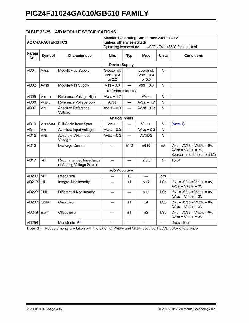
PIC24FJ1024GA610/GB610 FAMILY
TABLE 33-25: A/D MODULE SPECIFICATIONS
AC CHARACTERISTICSStandard Operating Conditions: 2.0V to 3.6V(unless otherwise stated)Operating temperature -40°C TA +85°C for Industrial
Param No.
Symbol Characteristic Min. Typ Max. Units Conditions
Device Supply
AD01 AVDD Module VDD Supply Greater of:VDD – 0.3
or 2.2
— Lesser of:VDD + 0.3
or 3.6
V
AD02 AVSS Module VSS Supply VSS – 0.3 — VSS + 0.3 V
Reference Inputs
AD05 VREFH Reference Voltage High AVSS + 1.7 — AVDD V
AD06 VREFL Reference Voltage Low AVSS — AVDD – 1.7 V
AD07 VREF Absolute ReferenceVoltage
AVSS – 0.3 — AVDD + 0.3 V
Analog Inputs
AD10 VINH-VINL Full-Scale Input Span VREFL — VREFH V (Note 1)
AD11 VIN Absolute Input Voltage AVSS – 0.3 — AVDD + 0.3 V
AD12 VINL Absolute VINL Input Voltage
AVSS – 0.3 — AVDD/3 V
AD13 Leakage Current — ±1.0 ±610 nA VINL = AVSS = VREFL = 0V, AVDD = VREFH = 3V,Source Impedance = 2.5 k
AD17 RIN Recommended Impedance of Analog Voltage Source
— — 2.5K 10-bit
A/D Accuracy
AD20B Nr Resolution — 12 — bits
AD21B INL Integral Nonlinearity — ±1 < ±2 LSb VINL = AVSS = VREFL = 0V, AVDD = VREFH = 3V
AD22B DNL Differential Nonlinearity — — < ±1 LSb VINL = AVSS = VREFL = 0V, AVDD = VREFH = 3V
AD23B GERR Gain Error — ±1 ±4 LSb VINL = AVSS = VREFL = 0V, AVDD = VREFH = 3V
AD24B EOFF Offset Error — ±1 ±2 LSb VINL = AVSS = VREFL = 0V, AVDD = VREFH = 3V
AD25B Monotonicity(1) — — — — Guaranteed
Note 1: Measurements are taken with the external VREF+ and VREF- used as the A/D voltage reference.
DS30010074E-page 436 2015-2017 Microchip Technology Inc.
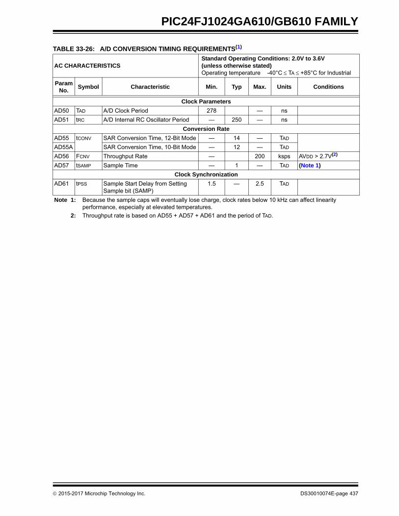
PIC24FJ1024GA610/GB610 FAMILY
TABLE 33-26: A/D CONVERSION TIMING REQUIREMENTS(1)
AC CHARACTERISTICSStandard Operating Conditions: 2.0V to 3.6V(unless otherwise stated)Operating temperature -40°C TA +85°C for Industrial
Param No.
Symbol Characteristic Min. Typ Max. Units Conditions
Clock Parameters
AD50 TAD A/D Clock Period 278 — ns
AD51 tRC A/D Internal RC Oscillator Period — 250 — ns
Conversion Rate
AD55 tCONV SAR Conversion Time, 12-Bit Mode — 14 — TAD
AD55A SAR Conversion Time, 10-Bit Mode — 12 — TAD
AD56 FCNV Throughput Rate — 200 ksps AVDD > 2.7V(2)
AD57 tSAMP Sample Time — 1 — TAD (Note 1)
Clock Synchronization
AD61 tPSS Sample Start Delay from Setting Sample bit (SAMP)
1.5 — 2.5 TAD
Note 1: Because the sample caps will eventually lose charge, clock rates below 10 kHz can affect linearity performance, especially at elevated temperatures.
2: Throughput rate is based on AD55 + AD57 + AD61 and the period of TAD.
2015-2017 Microchip Technology Inc. DS30010074E-page 437

PIC24FJ1024GA610/GB610 FAMILY
FIGURE 33-5: INL vs. CODE (10-BIT MODE)
FIGURE 33-6: DNL vs. CODE (10-BIT MODE)
0.2
0.15
0.1
-0.05
-0.1
0.05
-0.15
-0.2
0 200 400 600 800 1000
0
0 200 400 600 800 1000
0.2
0.15
0.1
-0.05
-0.1
0.05
-0.15
-0.2
0
DS30010074E-page 438 2015-2017 Microchip Technology Inc.

PIC24FJ1024GA610/GB610 FAMILY
FIGURE 33-7: INL vs. CODE (12-BIT MODE)
FIGURE 33-8: DNL vs. CODE (12-BIT MODE)(1)
0 1000 2000 3000 4000
0.8
0.6
0.4
-0.2
-0.4
0.2
-0.6
-0.8
0
0 1000 2000 3000 4000
0.8
0.6
0.4
-0.2
-0.4
0.2
-0.6
-0.8
0
Note 1: The following codes have marginal DNL and may result in a missing code: 1023, 2047, 3070 and 3071.
2015-2017 Microchip Technology Inc. DS30010074E-page 439

PIC24FJ1024GA610/GB610 FAMILY
NOTES:
DS30010074E-page 440 2015-2017 Microchip Technology Inc.

PIC24FJ1024GA610/GB610 FAMILY
34.0 PACKAGING INFORMATION
34.1 Package Marking Information
64-Lead TQFP (10x10x1 mm)
XXXXXXXXXXXXXXXXXXXX
YYWWNNN
Example
24FJ1024GB6061720017
XXXXXXXXXXX
64-Lead QFN (9x9x0.9 mm)
XXXXXXXXXXXYYWWNNN
PIC24FJ1024
Example
GB6061750017
Legend: XX...X Customer-specific informationY Year code (last digit of calendar year)YY Year code (last 2 digits of calendar year)WW Week code (week of January 1 is week ‘01’)NNN Alphanumeric traceability code
Note: In the event the full Microchip part number cannot be marked on one line, it willbe carried over to the next line, thus limiting the number of availablecharacters for customer-specific information.
2015-2017 Microchip Technology Inc. DS30010074E-page 441

PIC24FJ1024GA610/GB610 FAMILY
34.1 Package Marking Information (Continued)
100-Lead TQFP (12x12x1 mm)
XXXXXXXXXXXXXXXXXXXXXXXX
YYWWNNN
121-BGA (10x10x1.1 mm)
XXXXXXXXXXXXXXXXXXXXXX
YYWWNNN
Example
PIC24FJ1024GB610
1720017
Example
PIC24FJ1024
1710017GB610
DS30010074E-page 442 2015-2017 Microchip Technology Inc.

PIC24FJ1024GA610/GB610 FAMILY
34.2 Package Details
The following sections give the technical details of the packages.
BA
0.25 C
0.25 C
0.10 C A B0.05 C
(DATUM B)(DATUM A)
CSEATING
PLANE
NOTE 1
12
N
2XTOP VIEW
SIDE VIEW
BOTTOM VIEW
NOTE 1
12
N
0.10 C A B
0.10 C A B
0.10 C
0.08 C
Microchip Technology Drawing C04-213B Sheet 1 of 2
64-Lead Plastic Quad Flat, No Lead Package (MR) – 9x9x0.9 mm Body [QFN]
2X
64X
For the most current package drawings, please see the Microchip Packaging Specification located athttp://www.microchip.com/packaging
Note:
With 7.70 x 7.70 Exposed Pad [QFN]
A3
AA1
D
E
e
64X b
D2
E2
KL
e2
2015-2017 Microchip Technology Inc. DS30010074E-page 443
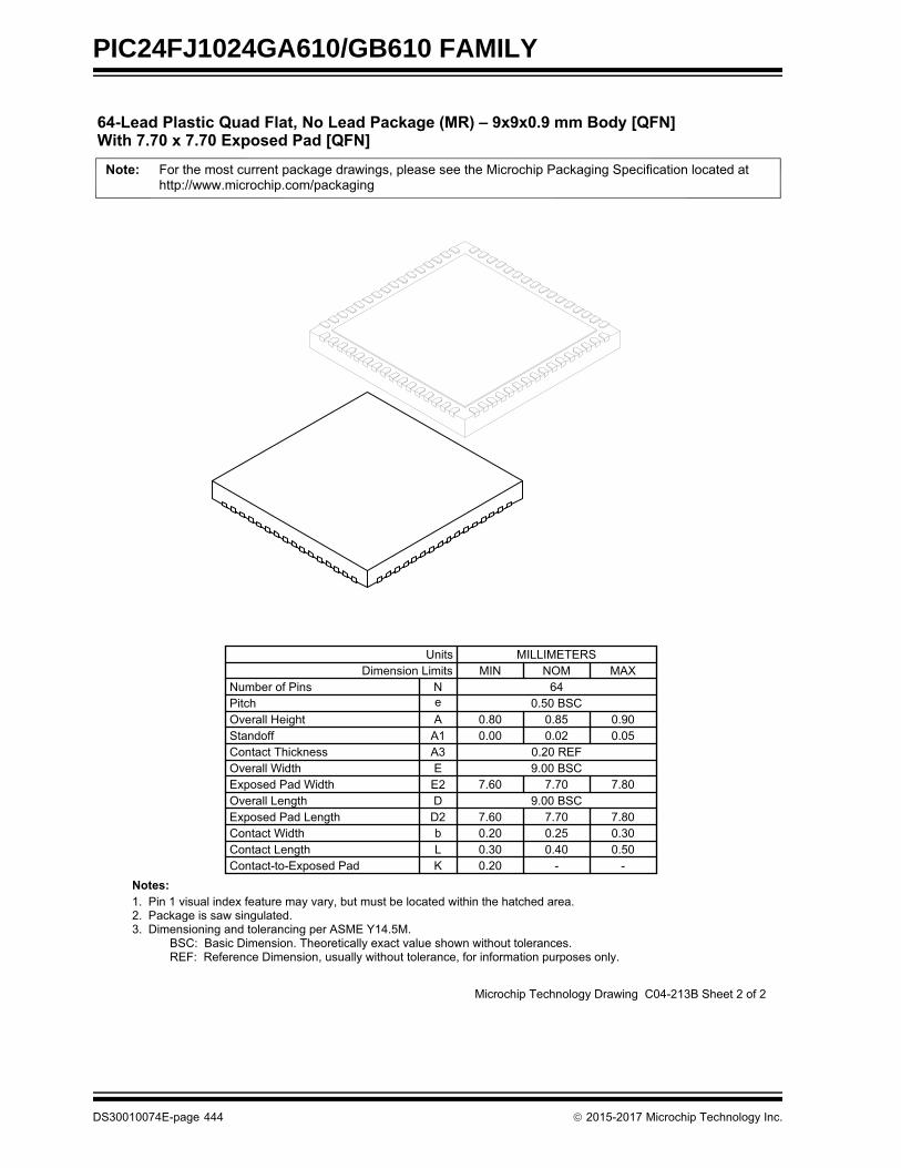
PIC24FJ1024GA610/GB610 FAMILY
Microchip Technology Drawing C04-213B Sheet 2 of 2
64-Lead Plastic Quad Flat, No Lead Package (MR) – 9x9x0.9 mm Body [QFN]
For the most current package drawings, please see the Microchip Packaging Specification located athttp://www.microchip.com/packaging
Note:
With 7.70 x 7.70 Exposed Pad [QFN]
0.500.30 0.40Contact Length LContact-to-Exposed Pad
REF: Reference Dimension, usually without tolerance, for information purposes only.
3.BSC: Basic Dimension. Theoretically exact value shown without tolerances.
1.Notes:
2.
K -0.20 -
Overall Height
Overall LengthExposed Pad Width
Contact Thickness
Number of Pins
Contact WidthExposed Pad Length
Overall Width
Standoff
Pitch
E2
D2b
D
A3E
A1
7.807.60 7.709.00 BSC
0.257.707.60
0.207.800.30
0.02
9.00 BSC0.20 REF
0.00 0.05
Dimension Limits
eA
N
UnitsMAXMIN NOM
0.50 BSC0.85
64
0.80 0.90
MILLIMETERS
Dimensioning and tolerancing per ASME Y14.5M.
Pin 1 visual index feature may vary, but must be located within the hatched area.Package is saw singulated.
DS30010074E-page 444 2015-2017 Microchip Technology Inc.

PIC24FJ1024GA610/GB610 FAMILY
Microchip Technology Drawing No. C04-2213B
64-Lead Plastic Quad Flat, No Lead Package (MR) – 9x9x0.9 mm Body [QFN]With 0.40 mm Contact Length and 7.70x7.70mm Exposed Pad
SILK SCREEN
12
64
C2
C1
W2
EV
ØVY1
X1
E
T2
RECOMMENDED LAND PATTERN
Dimension LimitsUnits
C2
Optional Center Pad Width
Contact Pad Spacing
Optional Center Pad Length
Contact Pitch
T2W2
7.507.50
MILLIMETERS
0.50 BSCMIN
EMAX
8.90
Contact Pad Length (X20)Contact Pad Width (X20)
Y1X1
0.900.30
NOM
C1Contact Pad Spacing 8.90
Contact Pad to Center Pad (X20) G 0.20Thermal Via Diameter VThermal Via Pitch EV
0.301.00
BSC: Basic Dimension. Theoretically exact value shown without tolerances.
Notes:Dimensioning and tolerancing per ASME Y14.5M
For best soldering results, thermal vias, if used, should be filled or tented to avoid solder loss duringreflow process
1.
2.
G
EV
For the most current package drawings, please see the Microchip Packaging Specification located athttp://www.microchip.com/packaging
Note:
2015-2017 Microchip Technology Inc. DS30010074E-page 445
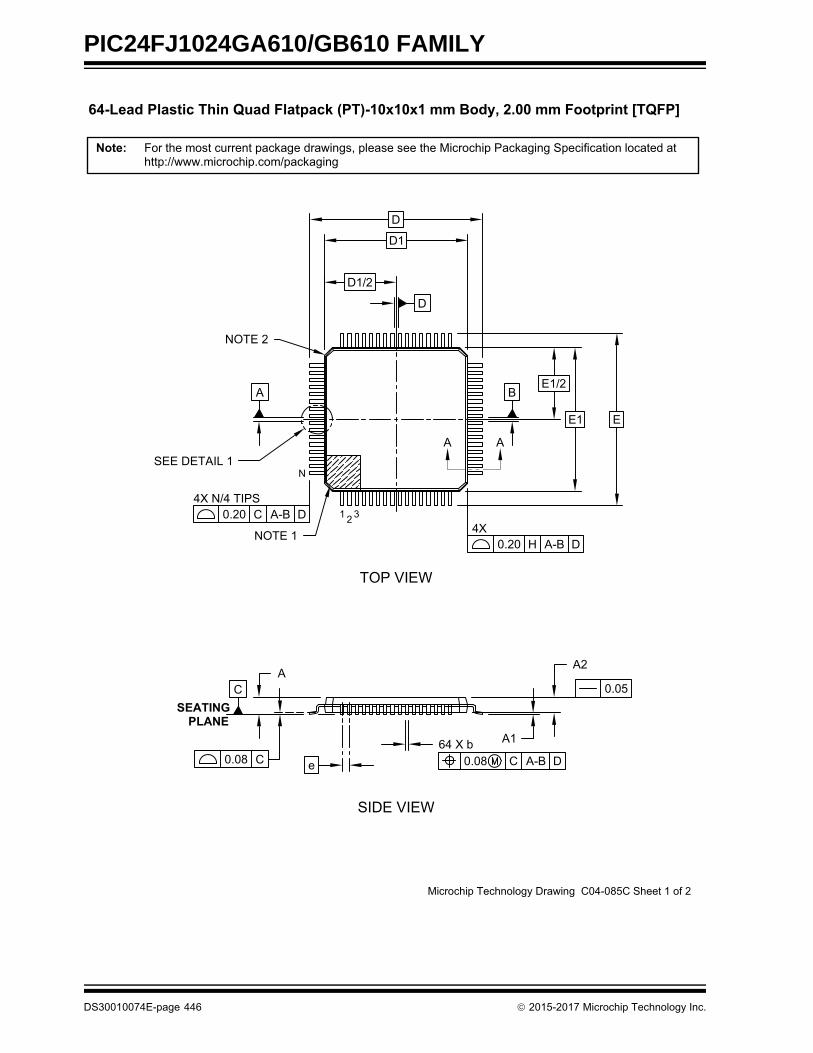
PIC24FJ1024GA610/GB610 FAMILY
0.20 C A-B D
64 X b0.08 C A-B D
CSEATING
PLANE
4X N/4 TIPS
TOP VIEW
SIDE VIEW
For the most current package drawings, please see the Microchip Packaging Specification located athttp://www.microchip.com/packaging
Note:
Microchip Technology Drawing C04-085C Sheet 1 of 2
64-Lead Plastic Thin Quad Flatpack (PT)-10x10x1 mm Body, 2.00 mm Footprint [TQFP]
D
EE1
D1
D
A B
0.20 H A-B D4X
D1/2
e
A
0.08 C
A1
A2
SEE DETAIL 1AA
E1/2
NOTE 1
NOTE 2
1 2 3
N
0.05
DS30010074E-page 446 2015-2017 Microchip Technology Inc.

PIC24FJ1024GA610/GB610 FAMILY
For the most current package drawings, please see the Microchip Packaging Specification located athttp://www.microchip.com/packaging
Note:
64-Lead Plastic Thin Quad Flatpack (PT)-10x10x1 mm Body, 2.00 mm Footprint [TQFP]
13°12°11°Mold Draft Angle Bottom13°12°11°Mold Draft Angle Top0.270.220.17bLead Width0.20-0.09cLead Thickness
10.00 BSCD1Molded Package Length10.00 BSCE1Molded Package Width12.00 BSCDOverall Length12.00 BSCEOverall Width
7°3.5°0°Foot Angle
0.750.600.45LFoot Length0.15-0.05A1Standoff1.051.000.95A2Molded Package Thickness1.20--AOverall Height
0.50 BSCeLead Pitch64NNumber of Leads
MAXNOMMINDimension LimitsMILLIMETERSUnits
Footprint L1 1.00 REF
2. Chamfers at corners are optional; size may vary.1. Pin 1 visual index feature may vary, but must be located within the hatched area.
4. Dimensioning and tolerancing per ASME Y14.5MBSC: Basic Dimension. Theoretically exact value shown without tolerances.REF: Reference Dimension, usually without tolerance, for information purposes only.
3. Dimensions D1 and E1 do not include mold flash or protrusions. Mold flash orprotrusions shall not exceed 0.25mm per side.
Notes:
Microchip Technology Drawing C04-085C Sheet 2 of 2
L(L1)
c
H
X
X=A—B OR D
e/2
DETAIL 1
SECTION A-A
2015-2017 Microchip Technology Inc. DS30010074E-page 447

PIC24FJ1024GA610/GB610 FAMILY
RECOMMENDED LAND PATTERN
For the most current package drawings, please see the Microchip Packaging Specification located athttp://www.microchip.com/packaging
Note:
Dimension LimitsUnits
C1Contact Pad SpacingContact Pad Spacing
Contact Pitch
C2
MILLIMETERS
0.50 BSCMIN
EMAX
11.4011.40
Contact Pad Length (X28)Contact Pad Width (X28)
Y1X1
1.500.30
BSC: Basic Dimension. Theoretically exact value shown without tolerances.
Notes:1. Dimensioning and tolerancing per ASME Y14.5M
Microchip Technology Drawing C04-2085B Sheet 1 of 1
GDistance Between Pads 0.20
NOM
64-Lead Plastic Thin Quad Flatpack (PT)-10x10x1 mm Body, 2.00 mm Footprint [TQFP]
C2
C1
E
G
Y1
X1
DS30010074E-page 448 2015-2017 Microchip Technology Inc.

PIC24FJ1024GA610/GB610 FAMILY
!"#$
% & !" #$ %! &'(!%&! %( % ")%% % " *&$ % %+ , &- & "."%!" &"$ %! "$ %! % # "/&& " & "% .0/
1*2 1 & % #%! ))%!%% .32 $ & '! !)%!%% '$$&%!
% & 3% & %! %4 ") ' % 4 $%% "%%%255)))&&54
6% 77..& 7&% 8 89 :
8!&( $7 " 8 7 "% 1*9 ; % < < " "4 4 / /%"$$ / < /3%7 % 7 / = /3%% 7 .33% > -/> >9 ?"% . 1*9 7 % 1*" "4 ?"% . 1*" "4 7 % 1*7 "4 < 7 "?"% ( - @ -"$% > > ->"$% 1%%& > > ->
D
D1
E
E1
e
bN
123NOTE 1 NOTE 2
c
LA1
L1
A
A2
α
βφ
) *1
2015-2017 Microchip Technology Inc. DS30010074E-page 449

PIC24FJ1024GA610/GB610 FAMILY
Note: For the most current package drawings, please see the Microchip Packaging Specification located at http://www.microchip.com/packaging
DS30010074E-page 450 2015-2017 Microchip Technology Inc.
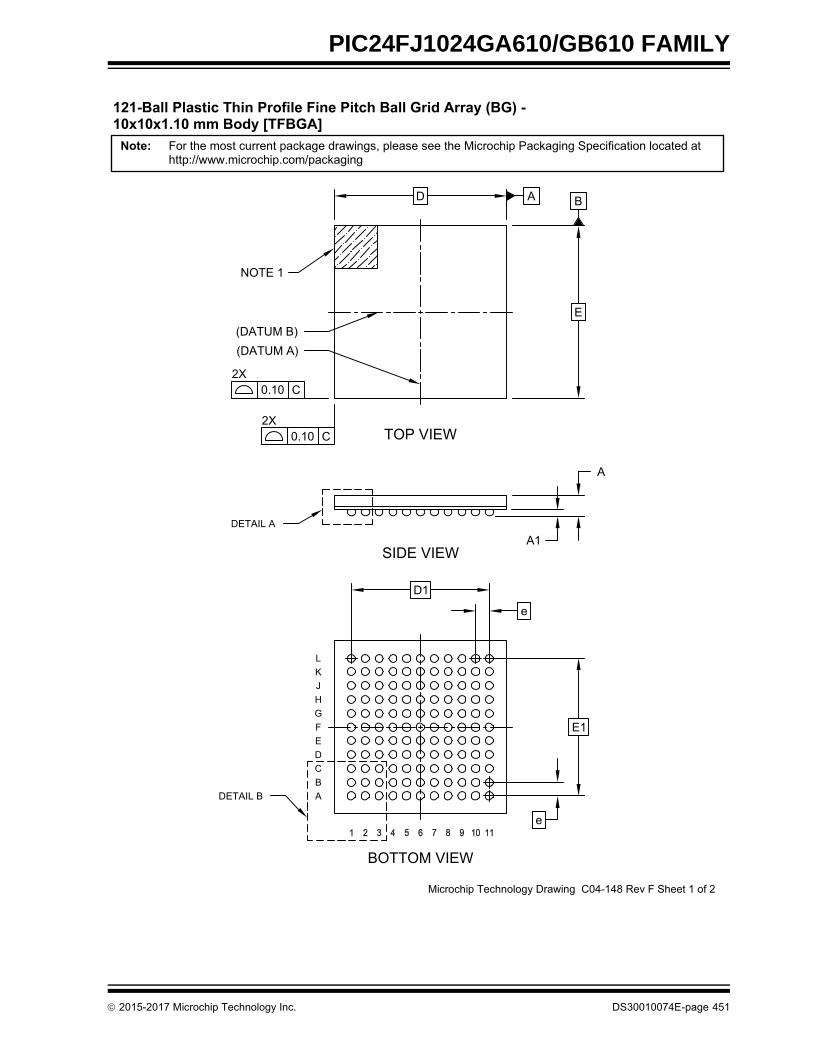
PIC24FJ1024GA610/GB610 FAMILY
BA
0.10 C
0.10 C
(DATUM B)(DATUM A)
2XTOP VIEW
SIDE VIEW
For the most current package drawings, please see the Microchip Packaging Specification located athttp://www.microchip.com/packaging
Note:
NOTE 1
Microchip Technology Drawing C04-148 Rev F Sheet 1 of 2
D
E
2X
LKJHGFEDCBADETAIL B
e
D1
E1
e
A
BOTTOM VIEW
DETAIL A
A1
121-Ball Plastic Thin Profile Fine Pitch Ball Grid Array (BG) -10x10x1.10 mm Body [TFBGA]
2015-2017 Microchip Technology Inc. DS30010074E-page 451

PIC24FJ1024GA610/GB610 FAMILY
Microchip Technology Drawing C04-148 Rev F Sheet 2 of 2
For the most current package drawings, please see the Microchip Packaging Specification located athttp://www.microchip.com/packaging
Note:
121-Ball Plastic Thin Profile Fine Pitch Ball Grid Array (BG) -
Dimension LimitsUnits
D
Overall Width
Overall LengthArray Length
Array Width
D1
E1E
MILLIMETERSMIN MAX
10.00 BSC
Contact Diameter b
Notes:1.
NOM
BSC: Basic Dimension. Theoretically exact value shown without tolerances.2.
REF: Reference Dimension, usually without tolerance, for information purposes only.
Ball Height A1Overall Height AContact Pitch e 0.80 BSCNumber of Contacts N 121
0.25
0.40
10.00 BSC
1.20
8.00 BSC
8.00 BSC
3.
1.101.000.30 0.35
NX Øb0.15 C A B0.08 C
C
0.10 C DETAIL A
DETAIL B
0.35 0.45
4. Ball interface to package body: 0.37mm nominal diameter.
Ball A1 visual index feature may vary, but must be located within the hatched area.Dimensioning and tolerancing per ASME Y14.5M.
The outer rows and colums of balls are located with respect to datums A and B.
10x10x1.10 mm Body [TFBGA]
DS30010074E-page 452 2015-2017 Microchip Technology Inc.
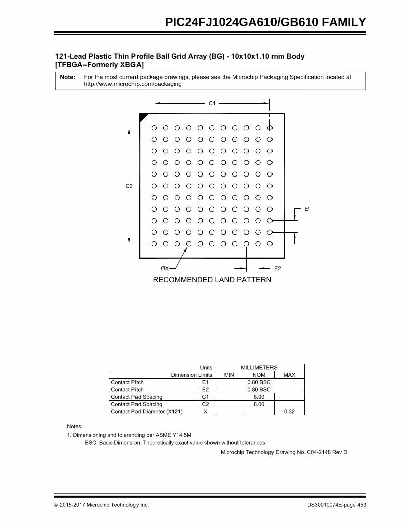
PIC24FJ1024GA610/GB610 FAMILY
2015-2017 Microchip Technology Inc. DS30010074E-page 453

PIC24FJ1024GA610/GB610 FAMILY
NOTES:
DS30010074E-page 454 2015-2017 Microchip Technology Inc.

PIC24FJ1024GA610/GB610 FAMILY
APPENDIX A: REVISION HISTORY
Revision A (March 2015)
Original data sheet for the PIC24FJ1024GA610/GB610 family of devices.
Revision B (November 2015)
This revision incorporates the following updates:
• Sections:
- Changed 12-bit conversion rate to 200 ksps in the Analog Features section on Page 1.
- Added Smart Card support (ISO 7816) information to the Peripheral Features section on Page 2.
- Added Section 9.3.1 “DCO Overview”.
- Added Section 25.4 “Achieving Maximum A/D Converter (ADC) Performance”.
- Added Section 30.2 “Unique Device Identifier (UDID)”.
- Updated Section 6.6 “Programming Operations”, Section 9.6 “PLL Oscillator Modes and USB Operation”, Section 9.6.1 “Considerations for USB Operation”, Section 9.7 “Reference Clock Output”, Section 9.8 “Secondary Oscil-lator”, Section 10.2 “Instruction-Based Power-Saving Modes”, Section 10.2.2 “Idle Mode”, Section 12.0 “Timer1”, Section 16.1 “Time Base Generator” and Section 33.0 “Electrical Characteristics”
• Registers
- Updated Register 5-1, Register 6-1, Register 7-1, Register 9-4, Register 9-5, Register 18-1, Register 22-3, Register 25-2, Register 25-3, Register 25-6, Register 25-7, Register 30-1, Register 30-5, Register 30-7, Register 30-8 and Register 30-9
• Figures:
- Updated Figure 2-1, Figure 9-2 and Figure 25-3
- Added Figure 33-5, Figure 33-6, Figure 33-7 and Figure 33-8
• Tables:
- Updated Table 2-1, Table 4-1, Table 4-2, Table 4-3, Table 4-10, Table 9-2, Table 9-3, Table 30-1, Table 33-3, Table 33-4, Table 33-5, Table 33-6, Table 33-7, Table 33-8, Table 33-9, Table 33-11, Table 33-12, Table 33-13, Table 33-15, Table 33-19, Table 33-24, Table 33-25 and Table 33-26.
• Examples:
- Updated Example 15-1.
• Other minor typographic changes and updates throughout the document.
Revision C (November 2015)
This revision incorporates the following updates:
• Tables:
- Updated Table 33-5 and Table 33-20.
• Figures:
- Updated Figure 33-8.
Revision D (December 2016)
This revision incorporates the following updates:
• Sections:
- Added Section 8.1.1 “Alternate Interrupt Vector Table”, Section 8.4.1 “INTCON1-INTCON4” and Section 10.2.5 “Exiting from Low-Voltage Retention Sleep”.
- Updated the “Referenced Sources” section. Updated Section 4.1.2 “Dual Parti-tion Flash Program Memory Organization” Section 4.1.5 “Code-Protect Configuration Bits”, Section 8.1.1 “Alternate Interrupt Vector Table”, Section 8.4 “Interrupt Con-trol and Status Registers”, Section 9.0 “Oscillator Configuration”, Section 10.2.4 “Low-Voltage Retention Regulator”, Section 11.3 “Interrupt-on-Change (IOC)”, Section 11.4.2 “Available Peripherals”, Section 17.0 “Serial Peripheral Interface (SPI)”, Section 22.0 “Real-Time Clock and Calendar with Timestamp” and Section 22.2.2 “Write Lock”.
• Tables:
- Added Table 8-1.
- Updated Table 4, Table 5, Table 6, Table 7, Table 1-3, Table 8-1, Table 9-1, Table 9-2, Table 9-3, Table 11-4, Table 33-4, Table 33-5, Table 33-6 and Table 33-7.
• Figures:
- Updated Figure 8-1, Figure 9-1, Figure 9-2 and Figure 22-1.
• Examples:
- Updated Example 11-3, Example 15-1 and Example 22-1.
• Equations:
- Updated Equation 15-2.
• Registers:
- Updated Register 7-1, Register 9-8, Register 17-1, Register 27-1 and Register 30-10.
2015-2017 Microchip Technology Inc. DS30010074E-page 455

PIC24FJ1024GA610/GB610 FAMILY
Revision E (July 2017)
This revision incorporates the following updates:
• Sections:
- Updated “Referenced Sources” section and Section 11.0 “I/O Ports” with correct “I/O Ports with Interrupt-on-Change (IOC)” (DS70005186) document reference.
• Pin Diagrams:
- Updated 64-Pin TQFP/QFN PIC24FJXXXXGA606 Diagram on Page 4, 64-Pin TQFP/QFN PIC24FJXXXXGB606 Diagram on Page 6, 100-Pin TQFP PIC24FJXXXXGA610 Diagram on Page 8, 100-Pin TQFP PIC24FJXXXXGB610 Diagram on Page 10, 121-Pin BGA PIC24FJXXXGA610 Diagram on Page 12 and 121-Pin BGA PIC24FJXXXGB610 Diagram on Page 15.
• Tables:
- Updated Table 2, Table 3, Table 4, Table 5, Table 6, Table 7, Table 4-7, Table 4-8 and Table 33-22.
DS30010074E-page 456 2015-2017 Microchip Technology Inc.

PIC24FJ1024GA610/GB610 FAMILY
INDEX
AA/D
Control Registers ...................................................... 350Extended DMA Operations ....................................... 349Operation .................................................................. 347Transfer Functions
10-Bit ................................................................ 36712-Bit ................................................................ 366
AC CharacteristicsA/D Conversion Timing Requirements...................... 437A/D Specifications..................................................... 436and Timing Parameters............................................. 429Capacitive Loading on Output Pins........................... 429CLKO and I/O Timing Requirements ........................ 434External Clock Timing Requirements........................ 430Internal DCO Accuracy ............................................. 433Internal RC Accuracy ................................................ 432Load Conditions for Device Timing ........................... 429Phase-Locked Loop Mode........................................ 431RC Oscillator Start-up Time ...................................... 432Reset and Brown-out Reset Requirements .............. 435
AssemblerMPASM Assembler................................................... 408
BBlock Diagrams
12-Bit A/D Converter................................................. 34812-Bit A/D Converter Analog Input Model................. 36516-Bit Asynchronous Timer3 and Timer5 ................. 18916-Bit Synchronous Timer2 and Timer4 ................... 18916-Bit Timer1 Module................................................ 18532-Bit Timer Mode .................................................... 212Accessing Program Memory Using
Table Instructions ............................................... 78Addressing for Table Registers................................... 89BDT Mapping for Endpoint Buffering Modes ............ 270Buffer Address Generation in PIA Mode................... 352CALL Stack Frame ............................................. 75CLCx Input Source Selection.................................... 339CLCx Logic Function Combinatorial Options ............ 338CLCx Module ............................................................ 337Comparator Voltage Reference ................................ 375Conceptual MCCPx/SCCPx Modules ....................... 209CPU Programmer’s Model .......................................... 49CRC Module ............................................................. 331CRC Shift Engine Detail............................................ 331CTMU Connections and Internal Configuration
for Capacitance Measurement.......................... 378CTMU Typical Connections and Internal
Configuration for Pulse Delay Generation ........ 379CTMU Typical Connections and Internal
Configuration for Time Measurement ............... 379Data Access from Program Space Address
Generation .......................................................... 77DMA Module ............................................................... 81Dual 16-Bit Timer Mode ............................................ 211EDS Address Generation for Read............................. 73EDS Address Generation for Write ............................. 74High/Low-Voltage Detect (HLVD) ............................. 387I2Cx Module.............................................................. 248Individual Comparator Configurations,
CREF = 0 .......................................................... 370
Individual Comparator Configurations, CREF = 1, CVREFP = 0................................... 370
Individual Comparator Configurations, CREF = 1, CVREFP = 1................................... 371
Input Capture x Module .................................... 193, 214MCLR Pin Connection Example ................................. 42On-Chip Regulator Connections............................... 403Oscillator Circuit Placement ....................................... 45Output Compare x (16-Bit Mode) ............................. 200Output Compare x (Double-Buffered,
16-Bit PWM Mode) ........................................... 202Output Compare x Module ....................................... 213PIC24F CPU Core ...................................................... 48PIC24FJ1024GA610/GB610 Family (General) .......... 25PLL Module .............................................................. 129PSV Operation (Lower Word)..................................... 80PSV Operation (Upper Word)..................................... 80Recommended Minimum Connections....................... 41Reference Clock Generator...................................... 130Reset System ............................................................. 97RTCC Module........................................................... 312Shared I/O Port Structure ......................................... 149SPIx Master, Frame Master Connection .................. 245SPIx Master, Frame Slave Connection .................... 246SPIx Master/Slave Connection
(Enhanced Buffer Modes)................................. 244SPIx Master/Slave Connection
(Standard Mode)............................................... 243SPIx Module (Enhanced Mode)................................ 229SPIx Slave, Frame Master Connection .................... 246SPIx Slave, Frame Slave Connection ...................... 246System Clock............................................................ 115Timer Clock Generator ............................................. 210Timer2/3 and Timer4/5 (32-Bit) ................................ 188Triple Comparator Module........................................ 369UARTx (Simplified) ................................................... 256USB OTG Bus-Powered Interface Example............. 267USB OTG Dual Power Mode Example..................... 267USB OTG Host Interface Example ........................... 268USB OTG Interface Example ................................... 268USB OTG Interrupt Funnel ....................................... 274USB OTG Module..................................................... 266USB OTG Self-Power Only Mode ............................ 267Watchdog Timer (WDT)............................................ 405
CC Compilers
MPLAB C18.............................................................. 408Capture/Compare/PWM/Timer
Auxiliary Output ........................................................ 215General Purpose Timer ............................................ 211Input Capture Mode.................................................. 214Output Compare Mode ............................................. 212Synchronization Sources.......................................... 219Time Base Generator ............................................... 210
Capture/Compare/PWM/Timer (MCCP, SCCP) ............... 209Charge Time Measurement Unit. See CTMU.CLC
Control Registers...................................................... 340Module-Specific Input Sources................................. 343
2015-2017 Microchip Technology Inc. DS30010074E-page 457

PIC24FJ1024GA610/GB610 FAMILY
Code ExamplesBasic Clock Switching ............................................... 127Configuring UART1 Input/Output Functions ............. 163Double-Word Flash Programming (C Language) ....... 96EDS Read from Program Memory in Assembly.......... 79EDS Read in Assembly............................................... 73EDS Write in Assembly ............................................... 74Erasing a Program Memory Block (C Language) ....... 94Initiating a Programming Sequence ............................ 94IOC Status Read/Clear in Assembly......................... 154Port Read/Write in Assembly .................................... 154Port Read/Write in C ................................................. 154PWRSAV Instruction Syntax...................................... 137Setting WRLOCK Bit ................................................. 313
Code Memory Programming ExampleDouble-Word Programming ........................................ 95Page Erase ................................................................. 93
Code Protection ................................................................ 406Comparator Voltage Reference ........................................ 375
Configuring................................................................ 375Configurable Logic Cell (CLC) .......................................... 337Configurable Logic Cell. See CLC.Configuration Bits.............................................................. 389Configuration Word Addresses ......................................... 390Core Features ..................................................................... 21CPU..................................................................................... 47
Arithmetic Logic Unit (ALU)......................................... 52Clocking Scheme ...................................................... 116Control Registers ........................................................ 50Core Registers ............................................................ 48Programmer’s Model................................................... 47
CRCData Shift Direction ................................................... 333Interrupt Operation.................................................... 333Polynomials............................................................... 332Setup Examples for 16 and 32-Bit Polynomials ........ 332User Interface ........................................................... 332
CTMUMeasuring Capacitance ............................................ 377Measuring Die Temperature ..................................... 380Measuring Time/Routing Current to
A/D Input Pin..................................................... 378Pulse Generation and Delay ..................................... 378
Customer Change Notification Service ............................. 463Customer Notification Service........................................... 463Customer OTP Memory .................................................... 406Customer Support ............................................................. 463Cyclic Redundancy Check. See CRC.
DData Memory Space ........................................................... 59
Extended Data Space (EDS) ...................................... 72Memory Map ............................................................... 59Near Data Space ........................................................ 60Organization, Alignment.............................................. 60SFR Space.................................................................. 60
Implemented Regions ......................................... 60Map, 0000h Block ............................................... 61Map, 0100h Block ............................................... 62Map, 0200h Block ............................................... 63Map, 0300h Block ............................................... 65Map, 0400h Block ............................................... 67Map, 0500h Block ............................................... 69Map, 0600h Block ............................................... 70Map, 0700h Block ............................................... 71
Software Stack............................................................ 75
DC CharacteristicsComparator Specifications........................................ 428Comparator Voltage Reference Specifications......... 428CTMU Current Source.............................................. 428 Current (BOR, WDT, HLVD, RTCC)...................... 424High/Low-Voltage Detect .......................................... 427I/O Pin Input Specifications....................................... 425I/O Pin Output Specifications.................................... 426Idle Current (IIDLE) .................................................... 422Internal Voltage Regulator Specifications................. 427Operating Current (IDD) ............................................ 422Power-Down Current (IPD)........................................ 423Program Memory ...................................................... 426Temperature and Voltage Specifications.................. 421Thermal Operating Conditions.................................. 420Thermal Packaging................................................... 420
Development Support ....................................................... 407Device Features
100 and 121-Pin Devices............................................ 2464-Pin Devices............................................................ 23
Device IDBit Field Descriptions ................................................ 402Registers .................................................................. 402
Direct Memory Access Controller. See DMA.DMA
Channel Trigger Sources............................................ 88Control Registers ........................................................ 84Peripheral Module Disable (PMD) Registers .............. 84Summary of Operations.............................................. 82Types of Data Transfers ............................................. 83Typical Setup .............................................................. 84
DMA Controller ................................................................... 22DNL................................................................................... 439
EElectrical Characteristics .................................................. 419
Absolute Maximum Ratings ...................................... 419V/F Graph (Industrial) ............................................... 420
Enhanced Parallel Master Port (EPMP) ........................... 299Enhanced Parallel Master Port. See EPMP.EPMP
Key Features ............................................................ 299Package Variations................................................... 299Pin Descriptions........................................................ 300PMDIN1, PMDIN2 Registers .................................... 299PMDOUT1, PMDOUT2 Registers ............................ 299
Equations16-Bit, 32-Bit CRC Polynomials................................ 332A/D Conversion Clock Period ................................... 365Baud Rate Reload Calculation.................................. 249Calculating Frequency Output .................................. 131Calculating the PWM Period..................................... 202Calculation for Maximum PWM Resolution .............. 203Estimating USB Transceiver Current
Consumption .................................................... 269Relationship Between Device and
SPIx Clock Speed............................................. 246UARTx Baud Rate with BRGH = 0 ........................... 257UARTx Baud Rate with BRGH = 1 ........................... 257
Errata .................................................................................. 19Extended Data Space (EDS) ............................................ 299
DS30010074E-page 458 2015-2017 Microchip Technology Inc.

PIC24FJ1024GA610/GB610 FAMILY
FFlash Program Memory ...................................................... 89
and Table Instructions................................................. 89Control Registers ........................................................ 90Double-Word Programming ........................................ 95Enhanced ICSP Operation.......................................... 90JTAG Operation .......................................................... 90Operations .................................................................. 90Programming Algorithm .............................................. 93RTSP Operation.......................................................... 90
GGuidelines for Getting Started with 16-Bit MCUs................ 41
Analog/Digital Pins Configuration During ICSP .......... 46External Oscillator Pins............................................... 45ICSP Pins.................................................................... 44Master Clear (MCLR) Pin............................................ 42Power Supply Pins...................................................... 42Unused I/Os ................................................................ 46Voltage Regulator Pin (VCAP) ..................................... 43
HHigh/Low-Voltage Detect (HLVD) ..................................... 387High/Low-Voltage Detect. See HLVD.
II/O Ports ............................................................................ 149
Analog Port Pins Configuration (ANSx) .................... 150Configuring Analog/Digital Function of I/O Pins........ 150Input Voltage Levels for Port/Pin Tolerated
Description Input ............................................... 150Open-Drain Configuration ......................................... 150Parallel (PIO) ............................................................ 149Peripheral Pin Select ................................................ 159Write/Read Timing .................................................... 150
I2CClock Rates............................................................... 249Communicating as Master in Single Master
Environment...................................................... 247Reserved Addresses................................................. 249Setting Baud Rate as Bus Master............................. 249Slave Address Masking ............................................ 249
In-Circuit Debugger ........................................................... 406Input Capture
32-Bit Cascaded Mode ............................................. 194Operations ................................................................ 194Synchronous and Trigger Modes.............................. 193
Input Capture with Dedicated Timers................................ 193Instruction Set
Overview ................................................................... 413Summary................................................................... 411Symbols Used in Opcode Descriptions..................... 412
Interfacing Program and Data Memory Spaces .................. 76Inter-Integrated Circuit. See I2C.Internet Address................................................................ 463Interrupt Controller ............................................................ 103
Alternate Interrupt Vector Table................................ 103Control and Status Registers .................................... 108Interrupt Vector Details ............................................. 105Interrupt Vector Table (IVT) ...................................... 103Reset Sequence ....................................................... 103Resources................................................................. 108Trap Vectors ............................................................. 104Vector Tables............................................................ 104
Interrupt-on-Change (IOC)................................................ 154
JJTAG Interface ................................................................. 406
KKey Features .................................................................... 389
LLow-Voltage/Retention Regulator..................................... 403
MMemory Organization ......................................................... 53
Program Memory Space............................................. 53Microchip Internet Web Site.............................................. 463MPLAB ASM30 Assembler, Linker, Librarian ................... 408MPLAB Integrated Development
Environment Software .............................................. 407MPLAB PM3 Device Programmer .................................... 409MPLAB REAL ICE In-Circuit Emulator System ................ 409MPLINK Object Linker/MPLIB Object Librarian ................ 408
NNear Data Space ................................................................ 60
OOn-Chip Voltage Regulator............................................... 403
POR.......................................................................... 403Standby Mode .......................................................... 403
Oscillator Configuration .................................................... 115Clock Switching ........................................................ 126
Sequence ......................................................... 126Configuration Bit Values for Clock Selection ............ 117Control Registers...................................................... 117FRC Self-Tuning....................................................... 127Initial Configuration on POR ..................................... 116USB Operation ......................................................... 128
Special Considerations..................................... 130Output Compare with Dedicated Timers........................... 199
Operating Modes ...................................................... 19932-Bit Cascaded Mode..................................... 199Synchronous and Trigger Modes ..................... 199
Operations ................................................................ 200
PPackaging
Details....................................................................... 443Marking..................................................................... 441
Peripheral Enable Bits ...................................................... 139Peripheral Module Disable Bits......................................... 139Peripheral Pin Select (PPS).............................................. 159
Available Peripherals and Pins................................. 159Configuration Control................................................ 162Considerations for Selection..................................... 163Control Registers...................................................... 164Input Mapping........................................................... 160Mapping Exceptions ................................................. 162Output Mapping ........................................................ 161Peripheral Priority ..................................................... 159Selectable Input Sources.......................................... 160Selectable Output Sources....................................... 161
PIC24FJ1024GA610/GB610 Family Pinout Descriptions..................................................... 26
2015-2017 Microchip Technology Inc. DS30010074E-page 459

PIC24FJ1024GA610/GB610 FAMILY
Pin DescriptionsPIC24FJXXXGA606 TQFP/QFN .................................. 5PIC24FJXXXGA610 BGA ........................................... 13PIC24FJXXXGA610 TQFP ........................................... 9PIC24FJXXXGB606 TQFP/QFN .................................. 7PIC24FJXXXGB610 BGA ........................................... 16PIC24FJXXXGB610 TQFP ......................................... 11
Power-Saving Features..................................................... 137Clock Frequency, Clock Switching............................ 137Doze Mode................................................................ 139Instruction-Based Modes .......................................... 137
Idle .................................................................... 138Sleep................................................................. 137
Interrupts Coincident with Instructions ...................... 138Low-Voltage Retention Regulator ............................. 138Selective Peripheral Power Control .......................... 139
Program Memory SpaceAccess Using Table Instructions ................................. 78Addressing .................................................................. 76Configuration Bits
Code-Protect....................................................... 58Overview ............................................................. 55
Configuration Word Addresses ................................... 57Customer OTP Memory .............................................. 58Dual Partition Configuration Words............................. 58Dual Partition Flash Memory Organization ................. 55Hard Memory Vectors ................................................. 55Memory Map ............................................................... 54Organization................................................................ 55Reading Data Using EDS ........................................... 79Sizes and Boundaries ................................................. 54
Program Verification.......................................................... 406Pulse-Width Modulation (PWM) Mode .............................. 201Pulse-Width Modulation. See PWM.PWM
Duty Cycle and Period .............................................. 202
RReal-Time Clock and Calendar (RTCC)............................ 311Real-Time Clock and Calendar. See RTCC.Reference Clock Output.................................................... 130Referenced Sources ........................................................... 20Register Summary
Peripheral Module Disable (PMD) ............................ 140Registers
AD1CHITH (A/D Scan Compare Hit, High Word)........................................................ 362
AD1CHITL (A/D Scan Compare Hit, Low Word)......................................................... 362
AD1CHS (A/D Sample Select) .................................. 360AD1CON1 (A/D Control 1) ........................................ 353AD1CON2 (A/D Control 2) ........................................ 355AD1CON3 (A/D Control 3) ........................................ 357AD1CON4 (A/D Control 4) ........................................ 358AD1CON5 (A/D Control 5) ........................................ 359AD1CSSH (A/D Input Scan Select, High Word) ....... 363AD1CSSL (A/D Input Scan Select, Low Word) ......... 363AD1CTMENH (A/D CTMU Enable, High Word)........ 364AD1CTMENL (A/D CTMU Enable, Low Word) ......... 364ALMDATEH (RTCC Alarm Date High)...................... 323ALMDATEL (RTCC Alarm Date Low) ....................... 323ALMTIMEH (RTCC Alarm Time High) ...................... 322ALMTIMEL (RTCC Alarm Time Low)........................ 322ANCFG (A/D Band Gap Reference
Configuration) ................................................... 361ANSA (PORTA Analog Function Selection).............. 151
ANSB (PORTB Analog Function Selection) ............. 151ANSC (PORTC Analog Function Selection) ............. 152ANSD (PORTD Analog Function Selection) ............. 152ANSE (PORTE Analog Function Selection) ............. 153ANSG (PORTG Analog Function Selection)............. 153BDnSTAT (Buffer Descriptor n Status Prototype, CPU
Mode (BD0STAT Through BD63STAT)) .......... 273BDnSTAT (Buffer Descriptor n Status Prototype, USB
Mode (BD0STAT Through BD63STAT)) .......... 272CCPxCON1H (CCPx Control 1 High) ....................... 218CCPxCON1L (CCPx Control 1 Low) ........................ 216CCPxCON2H (CCPx Control 2 High) ....................... 221CCPxCON2L (CCPx Control 2 Low) ........................ 220CCPxCON3H (CCPx Control 3 High) ....................... 223CCPxCON3L (CCPx Control 3 Low) ........................ 222CCPxSTATH (CCPx Status High) ............................ 225CCPxSTATL (CCPx Status Low).............................. 224CLCxCONH (CLCx Control High)............................. 341CLCxCONL (CLCx Control Low) .............................. 340CLCxGLSH (CLCx Gate Logic Input
Select High) ...................................................... 345CLCxGLSL (CLCx Gate Logic Input
Select Low)....................................................... 343CLCxSEL (CLCx Input MUX Select)......................... 342CLKDIV (Clock Divider) ............................................ 120CMSTAT (Comparator Module Status)..................... 373CMxCON (Comparator x Control,
Comparators 1 Through 3) ............................... 372CORCON (CPU Core Control) ........................... 51, 110CRCCON1 (CRC Control 1) ..................................... 334CRCCON2 (CRC Control 2) ..................................... 335CRCXORH (CRC XOR Polynomial, High Byte) ....... 336CRCXORL (CRC XOR Polynomial, Low Byte)......... 336CTMUCON1H (CTMU Control 1 High) ..................... 383CTMUCON1L (CTMU Control 1 Low) ...................... 381CTMUCON2L (CTMU Control 2 Low) ...................... 385CVRCON (Comparator Voltage
Reference Control) ........................................... 376DATEH (RTCC Date High) ....................................... 321DATEL (RTCC Date Low)......................................... 321DCOCON (Digitally Controlled
Oscillator Enable) ............................................. 123DCOTUN (Digitally Controlled Oscillator Tune)........ 122DMACHn (DMA Channel n Control) ........................... 86DMACON (DMA Engine Control)................................ 85DMAINTn (DMA Channel n Interrupt)......................... 87FBOOT Configuration ............................................... 391FBSLIM Configuration .............................................. 393FBTSEQ Configuration ............................................. 391FDEVOPT1 Configuration ........................................ 401FICD Configuration ................................................... 400FOSC Configuration ................................................. 396FOSCSEL Configuration........................................... 395FPOR Configuration ................................................. 399FSEC Configuration.................................................. 392FSIGN Configuration ................................................ 394FWDT Configuration ................................................. 397HLVDCON (High/Low-Voltage Detect Control) ........ 388I2CxCONH (I2Cx Control High) ................................ 252I2CxCONL (I2Cx Control Low) ................................. 250I2CxMSK (I2Cx Slave Mode Address Mask) ............ 254I2CxSTAT (I2Cx Status) ........................................... 253ICxCON1 (Input Capture x Control 1)....................... 195ICxCON2 (Input Capture x Control 2)....................... 196INTCON1 (Interrupt Control 1).................................. 111
DS30010074E-page 460 2015-2017 Microchip Technology Inc.

PIC24FJ1024GA610/GB610 FAMILY
INTCON2 (Interrupt Control 2).................................. 112INTCON4 (Interrupt Control 4).................................. 113INTTREG (Interrupt Control and Status)................... 114IOCFx (Interrupt-on-Change Flag x) ......................... 158IOCNx (Interrupt-on-Change Negative Edge x) ........ 157IOCPx (Interrupt-on-Change Positive Edge x).......... 157IOCSTAT (Interrupt-on-Change Status) ................... 156NVMCON (Flash Memory Control) ............................. 91OCxCON1 (Output Compare x Control 1) ................ 204OCxCON2 (Output Compare x Control 2) ................ 206OSCCON (Oscillator Control) ................................... 118OSCDIV (Oscillator Divisor)...................................... 124OSCFDIV (Oscillator Fractional Divisor)................... 125OSCTUN (FRC Oscillator Tune)............................... 121PADCON (Pad Configuration Control)...................... 309PADCON (Port Configuration) .................................. 155PMCON1 (EPMP Control 1) ..................................... 301PMCON2 (EPMP Control 2) ..................................... 302PMCON3 (EPMP Control 3) ..................................... 303PMCON4 (EPMP Control 4) ..................................... 304PMCSxBS (EPMP Chip Select x Base Address)...... 306PMCSxCF (EPMP Chip Select x Configuration)....... 305PMCSxMD (EPMP Chip Select x Mode) .................. 307PMD1 (Peripheral Module Disable 1) ....................... 141PMD2 (Peripheral Module Disable 2) ....................... 142PMD3 (Peripheral Module Disable 3) ....................... 143PMD4 (Peripheral Module Disable 4) ....................... 144PMD5 (Peripheral Module Disable 5) ....................... 145PMD6 (Peripheral Module Disable 6) ....................... 146PMD7 (Peripheral Module Disable 7) ....................... 146PMD8 (Peripheral Module Disable 8) ....................... 147PMSTAT (EPMP Status, Slave Mode)...................... 308RCON (Reset Control) ................................................ 98REFOCONH (Reference Oscillator
Control High)..................................................... 134REFOCONL (Reference Oscillator
Control Low) ..................................................... 133REFOTRIML (Reference Oscillator Trim Low) ......... 135RPINR0 (Peripheral Pin Select Input 0).................... 164RPINR1 (Peripheral Pin Select Input 1).................... 164RPINR11 (Peripheral Pin Select Input 11)................ 168RPINR12 (Peripheral Pin Select Input 12)................ 169RPINR14 (Peripheral Pin Select Input 14)................ 169RPINR15 (Peripheral Pin Select Input 15)................ 170RPINR17 (Peripheral Pin Select Input 17)................ 170RPINR18 (Peripheral Pin Select Input 18)................ 171RPINR19 (Peripheral Pin Select Input 19)................ 171RPINR2 (Peripheral Pin Select Input 2).................... 165RPINR20 (Peripheral Pin Select Input 20)................ 172RPINR21 (Peripheral Pin Select Input 21)................ 172RPINR22 (Peripheral Pin Select Input 22)................ 173RPINR23 (Peripheral Pin Select Input 23)................ 173RPINR25 (Peripheral Pin Select Input 25)................ 174RPINR27 (Peripheral Pin Select Input 27)................ 174RPINR28 (Peripheral Pin Select Input 28)................ 175RPINR29 (Peripheral Pin Select Input 29)................ 175RPINR3 (Peripheral Pin Select Input 3).................... 165RPINR4 (Peripheral Pin Select Input 4).................... 166RPINR5 (Peripheral Pin Select Input 5).................... 166RPINR6 (Peripheral Pin Select Input 6).................... 167RPINR7 (Peripheral Pin Select Input 7).................... 167RPINR8 (Peripheral Pin Select Input 8).................... 168RPOR0 (Peripheral Pin Select Output 0).................. 176RPOR1 (Peripheral Pin Select Output 1).................. 176RPOR10 (Peripheral Pin Select Output 10).............. 181
RPOR11 (Peripheral Pin Select Output 11) ............. 181RPOR12 (Peripheral Pin Select Output 12) ............. 182RPOR13 (Peripheral Pin Select Output 13) ............. 182RPOR14 (Peripheral Pin Select Output 14) ............. 183RPOR15 (Peripheral Pin Select Output 15) ............. 183RPOR2 (Peripheral Pin Select Output 2) ................. 177RPOR3 (Peripheral Pin Select Output 3) ................. 177RPOR4 (Peripheral Pin Select Output 4) ................. 178RPOR5 (Peripheral Pin Select Output 5) ................. 178RPOR6 (Peripheral Pin Select Output 6) ................. 179RPOR7 (Peripheral Pin Select Output 7) ................. 179RPOR8 (Peripheral Pin Select Output 8) ................. 180RPOR9 (Peripheral Pin Select Output 9) ................. 180RTCCON1H (RTCC Control 1 High) ........................ 315RTCCON1L (RTCC Control 1 Low).......................... 314RTCCON2H (RTCC Control 2 High) ........................ 317RTCCON2L (RTCC Control 2 Low).......................... 316RTCCON3L (RTCC Control 3 Low).......................... 318RTCSTATL (RTCC Status Low)............................... 319SPIxBRGL (SPIx Baud Rate Generator Low) .......... 239SPIxBUFH (SPIx Buffer High) .................................. 238SPIxBUFL (SPIx Buffer Low).................................... 238SPIxCON1H (SPIx Control 1 High) .......................... 232SPIxCON1L (SPIx Control 1 Low)............................ 230SPIxCON2L (SPIx Control 2 Low)............................ 234SPIxIMSKH (SPIx Interrupt Mask High) ................... 241SPIxIMSKL (SPIx Interrupt Mask Low)..................... 240SPIxSTATH (SPIx Status High)................................ 237SPIxSTATL (SPIx Status Low) ................................. 235SPIxURDTH (SPIx Underrun Data High) ................. 242SPIxURDTL (SPIx Underrun Data Low)................... 242SR (ALU STATUS) ............................................. 50, 109T1CON (Timer1 Control) .......................................... 186TIMEH (RTCC Time High)........................................ 320TIMEL (RTCC Time Low) ......................................... 320TSADATEH (RTCC Timestamp A Date High).......... 327TSADATEL (RTCC Timestamp A Date Low) ........... 326TSATIMEH (RTCC Timestamp A Time High) .......... 325TSATIMEL (RTCC Timestamp A Time Low)............ 324TxCON (Timer2/Timer4 Control) .............................. 190TyCON (Timer3/Timer5 Control) .............................. 192U10TGSTAT (USB OTG Status, Host Mode)........... 280U1ADDR (USB Address) .......................................... 286U1CNFG1 (USB Configuration 1)............................. 288U1CNFG2 (USB Configuration 2)............................. 289U1CON (USB Control, Device Mode)....................... 284U1CON (USB Control, Host Mode) .......................... 285U1EIE (USB Error Interrupt Enable) ......................... 296U1EIR (USB Error Interrupt Status).......................... 295U1EPn (USB Endpoint n Control)............................. 297U1IE (USB Interrupt Enable, All Modes) .................. 294U1IR (USB Interrupt Status, Device Mode) .............. 292U1IR (USB Interrupt Status, Host Mode).................. 293U1OTGCON (USB OTG Control) ............................. 281U1OTGIE (USB OTG Interrupt Enable,
Host Mode) ....................................................... 291U1OTGIR (USB OTG Interrupt Status,
Host Mode) ....................................................... 290U1PWRC (USB Power Control) ............................... 282U1SOF (USB OTG Start-of-Token Threshold,
Host Mode) ....................................................... 287U1STAT (USB Status) .............................................. 283U1TOK (USB Token, Host Mode) ............................ 286UxADMD (UARTx Address Detect and Match) ........ 264UxBRG (UARTx Baud Rate Generator) ................... 264
2015-2017 Microchip Technology Inc. DS30010074E-page 461
PIC24FJ1024GA610/GB610 FAMILY
UxMODE (UARTx Mode).......................................... 259UxRXREG (UARTx Receive,
Normally Read-Only) ........................................ 263UxSTA (UARTx Status and Control) ......................... 261UxTXREG (UARTx Transmit,
Normally Write-Only)......................................... 263Resets
BOR (Brown-out Reset) .............................................. 97Brown-out Reset (BOR) ............................................ 100Clock Source Selection............................................. 100CM (Configuration Mismatch Reset) ........................... 97Delay Times .............................................................. 101Device Times ............................................................ 100IOPUWR (Illegal Opcode Reset) ................................ 97MCLR (Master Clear Pin Reset) ................................. 97POR (Power-on Reset) ............................................... 97RCON Flags, Operation.............................................. 99SFR States................................................................ 100SWR (RESET Instruction)........................................... 97TRAPR (Trap Conflict Reset)...................................... 97UWR (Uninitialized W Register Reset)........................ 97WDT (Watchdog Timer Reset).................................... 97
Revision History ................................................................ 455RTCC
Alarm Configuration .................................................. 328Alarm Mask Settings (figure)..................................... 329Alarm Value Registers .............................................. 322Calibration................................................................. 328Clock Source Selection............................................. 313Control Registers ...................................................... 314Event Timestamping ................................................. 330Power Control ........................................................... 329Register Mapping...................................................... 313RTCVAL Register Mappings ..................................... 317Source Clock............................................................. 311Timestamp Registers ................................................ 324Value Registers......................................................... 320Write Lock ................................................................. 313
SSecondary Oscillator Operation ........................................ 132Serial Peripheral Interface (SPI) ....................................... 227Serial Peripheral Interface. See SPI.Software Simulator (MPLAB SIM)..................................... 409Software Stack .................................................................... 75Special Features ................................................................. 22Special Features of the CPU............................................. 389SPI
Audio Mode Operation .............................................. 229Control Registers ...................................................... 230Master Mode Operation ............................................ 228Slave Mode Operation .............................................. 228
TTimer1 ............................................................................... 185Timer2/3 and Timer4/5...................................................... 187Timing Diagrams
CLKO and I/O Characteristics................................... 434DNL vs. Code (10-Bit Mode) ..................................... 438DNL vs. Code (12-Bit Mode) ..................................... 439External Clock........................................................... 430INL vs. Code (10-Bit Mode) ...................................... 438INL vs. Code (12-Bit Mode) ...................................... 439
Triple Comparator ............................................................. 369Triple Comparator Module ................................................ 369
UUART
Baud Rate Generator (BRG) .................................... 257Infrared Support........................................................ 258Operation of UxCTS and UxRTS Pins...................... 258Receiving
8-Bit or 9-Bit Data Mode ................................... 258Transmitting
8-Bit Data Mode................................................ 2589-Bit Data Mode................................................ 258Break and Sync Sequence ............................... 258
Unique Device Identifier (UDID) ....................................... 402Addresses................................................................. 402
Universal Asynchronous Receiver Transmitter. See UART.Universal Serial Bus. See USB OTG.USB OTG.......................................................................... 265
Buffer DescriptorsAssignment in Different Buffering Modes ......... 271
Buffer Descriptors and BDT...................................... 270Control Registers ...................................................... 279Device Mode Operation............................................ 275DMA Interface........................................................... 271Hardware
CalculatingTransceiver Power Requirements ............ 269
Hardware Configuration............................................ 267Device Mode..................................................... 267Host and OTG Modes....................................... 268
Host Mode Operation................................................ 276Interrupts .................................................................. 274Interrupts and USB Transactions.............................. 275Operation .................................................................. 278
HNP .................................................................. 279SRP .................................................................. 278
WWatchdog Timer (WDT).................................................... 404
Control Register........................................................ 404Windowed Operation ................................................ 404
WWW Address ................................................................. 463WWW, On-Line Support ..................................................... 19
DS30010074E-page 462 2015-2017 Microchip Technology Inc.

PIC24FJ1024GA610/GB610 FAMILY
THE MICROCHIP WEB SITE
Microchip provides online support via our WWW site atwww.microchip.com. This web site is used as a meansto make files and information easily available tocustomers. Accessible by using your favorite Internetbrowser, the web site contains the following informa-tion:
• Product Support – Data sheets and errata, appli-cation notes and sample programs, design resources, user’s guides and hardware support documents, latest software releases and archived software
• General Technical Support – Frequently Asked Questions (FAQ), technical support requests, online discussion groups, Microchip consultant program member listing
• Business of Microchip – Product selector and ordering guides, latest Microchip press releases, listing of seminars and events, listings of Micro-chip sales offices, distributors and factory repre-sentatives
CUSTOMER CHANGE NOTIFICATION SERVICE
Microchip’s customer notification service helps keepcustomers current on Microchip products. Subscriberswill receive e-mail notification whenever there arechanges, updates, revisions or errata related to a spec-ified product family or development tool of interest.
To register, access the Microchip web site atwww.microchip.com. Under “Support”, click on “Cus-tomer Change Notification” and follow the registrationinstructions.
CUSTOMER SUPPORT
Users of Microchip products can receive assistancethrough several channels:
• Distributor or Representative
• Local Sales Office
• Field Application Engineer (FAE)
• Technical Support
Customers should contact their distributor, representa-tive or Field Application Engineer (FAE) for support.Local sales offices are also available to help custom-ers. A listing of sales offices and locations is included inthe back of this document.
Technical support is available through the web siteat: http://microchip.com/support
2015-2017 Microchip Technology Inc. DS30010074E-page 463

PIC24FJ1024GA610/GB610 FAMILY
NOTES:
DS30010074E-page 464 2015-2017 Microchip Technology Inc.

PIC24FJ1024GA610/GB610 FAMILY
PRODUCT IDENTIFICATION SYSTEM
To order or obtain information, e.g., on pricing or delivery, refer to the factory or the listed sales office.
PART NO. X /XX XXX
PatternPackageTemperatureRange
Device
Device: PIC24FJ1024GA610/GB610
Tape and Reel Option:
Blank = Standard Packaging (tube or tray)T = Tape and Reel(1)
Temperature Range:
I = -40C to +85C (Industrial)E = -40C to +125C (Extended)
Package: MR = QFN (Plastic Quad Flat)PT = TQFP (Plastic Thin Quad Flatpack)BG = TFBGA (Plastic Thin Profile)
Pattern: QTP, SQTP, Code or Special Requirements (blank otherwise)
Examples:
a) PIC24FJ1024GB606-I/MR = Industrial Temperature, 64-Pin QFN Package.
b) PIC24FJ1024GB610-I/PT = Industrial Temperature, 100-Pin TQFP package.
c) PIC24FJ1024GB610-I/BG = Industrial Temperature, 121-Pin TFBGA package.
Note 1: Tape and Reel identifier only appears in the catalog part number description. This identi-fier is used for ordering purposes and is not printed on the device package. Check with your Microchip Sales Office for package availability with the Tape and Reel option.
[X](1)
Tape and ReelOption
2015-2017 Microchip Technology Inc. DS30010074E-page 465

PIC24FJ1024GA610/GB610 FAMILY
NOTES:
DS30010074E-page 466 2015-2017 Microchip Technology Inc.

Note the following details of the code protection feature on Microchip devices:
• Microchip products meet the specification contained in their particular Microchip Data Sheet.
• Microchip believes that its family of products is one of the most secure families of its kind on the market today, when used in the intended manner and under normal conditions.
• There are dishonest and possibly illegal methods used to breach the code protection feature. All of these methods, to our knowledge, require using the Microchip products in a manner outside the operating specifications contained in Microchip’s Data Sheets. Most likely, the person doing so is engaged in theft of intellectual property.
• Microchip is willing to work with the customer who is concerned about the integrity of their code.
• Neither Microchip nor any other semiconductor manufacturer can guarantee the security of their code. Code protection does not mean that we are guaranteeing the product as “unbreakable.”
Code protection is constantly evolving. We at Microchip are committed to continuously improving the code protection features of ourproducts. Attempts to break Microchip’s code protection feature may be a violation of the Digital Millennium Copyright Act. If such actsallow unauthorized access to your software or other copyrighted work, you may have a right to sue for relief under that Act.
Information contained in this publication regarding deviceapplications and the like is provided only for your convenienceand may be superseded by updates. It is your responsibility toensure that your application meets with your specifications.MICROCHIP MAKES NO REPRESENTATIONS ORWARRANTIES OF ANY KIND WHETHER EXPRESS ORIMPLIED, WRITTEN OR ORAL, STATUTORY OROTHERWISE, RELATED TO THE INFORMATION,INCLUDING BUT NOT LIMITED TO ITS CONDITION,QUALITY, PERFORMANCE, MERCHANTABILITY ORFITNESS FOR PURPOSE. Microchip disclaims all liabilityarising from this information and its use. Use of Microchipdevices in life support and/or safety applications is entirely atthe buyer’s risk, and the buyer agrees to defend, indemnify andhold harmless Microchip from any and all damages, claims,suits, or expenses resulting from such use. No licenses areconveyed, implicitly or otherwise, under any Microchipintellectual property rights unless otherwise stated.
2015-2017 Microchip Technology Inc.
Microchip received ISO/TS-16949:2009 certification for its worldwide headquarters, design and wafer fabrication facilities in Chandler and Tempe, Arizona; Gresham, Oregon and design centers in California and India. The Company’s quality system processes and procedures are for its PIC® MCUs and dsPIC® DSCs, KEELOQ® code hopping devices, Serial EEPROMs, microperipherals, nonvolatile memory and analog products. In addition, Microchip’s quality system for the design and manufacture of development systems is ISO 9001:2000 certified.
QUALITY MANAGEMENT SYSTEM CERTIFIED BY DNV
== ISO/TS 16949 ==
Trademarks
The Microchip name and logo, the Microchip logo, AnyRate, AVR, AVR logo, AVR Freaks, BeaconThings, BitCloud, CryptoMemory, CryptoRF, dsPIC, FlashFlex, flexPWR, Heldo, JukeBlox, KEELOQ, KEELOQ logo, Kleer, LANCheck, LINK MD, maXStylus, maXTouch, MediaLB, megaAVR, MOST, MOST logo, MPLAB, OptoLyzer, PIC, picoPower, PICSTART, PIC32 logo, Prochip Designer, QTouch, RightTouch, SAM-BA, SpyNIC, SST, SST Logo, SuperFlash, tinyAVR, UNI/O, and XMEGA are registered trademarks of Microchip Technology Incorporated in the U.S.A. and other countries.
ClockWorks, The Embedded Control Solutions Company, EtherSynch, Hyper Speed Control, HyperLight Load, IntelliMOS, mTouch, Precision Edge, and Quiet-Wire are registered trademarks of Microchip Technology Incorporated in the U.S.A.
Adjacent Key Suppression, AKS, Analog-for-the-Digital Age, Any Capacitor, AnyIn, AnyOut, BodyCom, chipKIT, chipKIT logo, CodeGuard, CryptoAuthentication, CryptoCompanion, CryptoController, dsPICDEM, dsPICDEM.net, Dynamic Average Matching, DAM, ECAN, EtherGREEN, In-Circuit Serial Programming, ICSP, Inter-Chip Connectivity, JitterBlocker, KleerNet, KleerNet logo, Mindi, MiWi, motorBench, MPASM, MPF, MPLAB Certified logo, MPLIB, MPLINK, MultiTRAK, NetDetach, Omniscient Code Generation, PICDEM, PICDEM.net, PICkit, PICtail, PureSilicon, QMatrix, RightTouch logo, REAL ICE, Ripple Blocker, SAM-ICE, Serial Quad I/O, SMART-I.S., SQI, SuperSwitcher, SuperSwitcher II, Total Endurance, TSHARC, USBCheck, VariSense, ViewSpan, WiperLock, Wireless DNA, and ZENA are trademarks of Microchip Technology Incorporated in the U.S.A. and other countries.
SQTP is a service mark of Microchip Technology Incorporated in the U.S.A.
Silicon Storage Technology is a registered trademark of Microchip Technology Inc. in other countries.
GestIC is a registered trademark of Microchip Technology Germany II GmbH & Co. KG, a subsidiary of Microchip Technology Inc., in other countries.
All other trademarks mentioned herein are property of their respective companies.
© 2015-2017, Microchip Technology Incorporated, All Rights Reserved.
ISBN: 978-1-5224-1978-5
DS30010074E-page 467

DS30010074E-page 468 2015-2017 Microchip Technology Inc.
AMERICASCorporate Office2355 West Chandler Blvd.Chandler, AZ 85224-6199Tel: 480-792-7200 Fax: 480-792-7277Technical Support: http://www.microchip.com/supportWeb Address: www.microchip.com
AtlantaDuluth, GA Tel: 678-957-9614 Fax: 678-957-1455
Austin, TXTel: 512-257-3370
BostonWestborough, MA Tel: 774-760-0087 Fax: 774-760-0088
ChicagoItasca, IL Tel: 630-285-0071 Fax: 630-285-0075
DallasAddison, TX Tel: 972-818-7423 Fax: 972-818-2924
DetroitNovi, MI Tel: 248-848-4000
Houston, TX Tel: 281-894-5983
IndianapolisNoblesville, IN Tel: 317-773-8323Fax: 317-773-5453Tel: 317-536-2380
Los AngelesMission Viejo, CA Tel: 949-462-9523Fax: 949-462-9608Tel: 951-273-7800
Raleigh, NC Tel: 919-844-7510
New York, NY Tel: 631-435-6000
San Jose, CA Tel: 408-735-9110Tel: 408-436-4270
Canada - TorontoTel: 905-695-1980 Fax: 905-695-2078
ASIA/PACIFICAsia Pacific OfficeSuites 3707-14, 37th FloorTower 6, The GatewayHarbour City, Kowloon
Hong KongTel: 852-2943-5100Fax: 852-2401-3431
Australia - SydneyTel: 61-2-9868-6733Fax: 61-2-9868-6755
China - BeijingTel: 86-10-8569-7000 Fax: 86-10-8528-2104
China - ChengduTel: 86-28-8665-5511Fax: 86-28-8665-7889
China - ChongqingTel: 86-23-8980-9588Fax: 86-23-8980-9500
China - DongguanTel: 86-769-8702-9880
China - GuangzhouTel: 86-20-8755-8029
China - HangzhouTel: 86-571-8792-8115 Fax: 86-571-8792-8116
China - Hong Kong SARTel: 852-2943-5100 Fax: 852-2401-3431
China - NanjingTel: 86-25-8473-2460Fax: 86-25-8473-2470
China - QingdaoTel: 86-532-8502-7355Fax: 86-532-8502-7205
China - ShanghaiTel: 86-21-3326-8000 Fax: 86-21-3326-8021
China - ShenyangTel: 86-24-2334-2829Fax: 86-24-2334-2393
China - ShenzhenTel: 86-755-8864-2200 Fax: 86-755-8203-1760
China - WuhanTel: 86-27-5980-5300Fax: 86-27-5980-5118
China - XianTel: 86-29-8833-7252Fax: 86-29-8833-7256
ASIA/PACIFICChina - XiamenTel: 86-592-2388138 Fax: 86-592-2388130
China - ZhuhaiTel: 86-756-3210040 Fax: 86-756-3210049
India - BangaloreTel: 91-80-3090-4444 Fax: 91-80-3090-4123
India - New DelhiTel: 91-11-4160-8631Fax: 91-11-4160-8632
India - PuneTel: 91-20-3019-1500
Japan - OsakaTel: 81-6-6152-7160 Fax: 81-6-6152-9310
Japan - TokyoTel: 81-3-6880- 3770 Fax: 81-3-6880-3771
Korea - DaeguTel: 82-53-744-4301Fax: 82-53-744-4302
Korea - SeoulTel: 82-2-554-7200Fax: 82-2-558-5932 or 82-2-558-5934
Malaysia - Kuala LumpurTel: 60-3-6201-9857Fax: 60-3-6201-9859
Malaysia - PenangTel: 60-4-227-8870Fax: 60-4-227-4068
Philippines - ManilaTel: 63-2-634-9065Fax: 63-2-634-9069
SingaporeTel: 65-6334-8870Fax: 65-6334-8850
Taiwan - Hsin ChuTel: 886-3-5778-366Fax: 886-3-5770-955
Taiwan - KaohsiungTel: 886-7-213-7830
Taiwan - TaipeiTel: 886-2-2508-8600 Fax: 886-2-2508-0102
Thailand - BangkokTel: 66-2-694-1351Fax: 66-2-694-1350
EUROPEAustria - WelsTel: 43-7242-2244-39Fax: 43-7242-2244-393
Denmark - CopenhagenTel: 45-4450-2828 Fax: 45-4485-2829
Finland - EspooTel: 358-9-4520-820
France - ParisTel: 33-1-69-53-63-20 Fax: 33-1-69-30-90-79
France - Saint CloudTel: 33-1-30-60-70-00
Germany - GarchingTel: 49-8931-9700Germany - HaanTel: 49-2129-3766400
Germany - HeilbronnTel: 49-7131-67-3636
Germany - KarlsruheTel: 49-721-625370
Germany - MunichTel: 49-89-627-144-0 Fax: 49-89-627-144-44
Germany - RosenheimTel: 49-8031-354-560
Israel - Ra’anana Tel: 972-9-744-7705
Italy - Milan Tel: 39-0331-742611 Fax: 39-0331-466781
Italy - PadovaTel: 39-049-7625286
Netherlands - DrunenTel: 31-416-690399 Fax: 31-416-690340
Norway - TrondheimTel: 47-7289-7561
Poland - WarsawTel: 48-22-3325737
Romania - BucharestTel: 40-21-407-87-50
Spain - MadridTel: 34-91-708-08-90Fax: 34-91-708-08-91
Sweden - GothenbergTel: 46-31-704-60-40
Sweden - StockholmTel: 46-8-5090-4654
UK - WokinghamTel: 44-118-921-5800Fax: 44-118-921-5820
Worldwide Sales and Service
11/07/16