Bt8960, Single-Chip 2B1Q Transceiver - Mindspeed Technologies
104
Bt8960 Single-Chip 2B1Q Transceiver The Bt8960 is a full-duplex 2B1Q transceiver based on Rockwell’s HDSL technol- ogy. It supports Nx64 kbps transmission of more than 18,000 feet over 26 AWG copper telephone wire without repeaters. Small size and low power dissipation make the Bt8960 ideal for line-powered voice pairgain systems capable of provid- ing four or six clear 64 kbps channels. The Bt8960 is a highly integrated device that includes all of the active circuitry needed for a complete 2B1Q transceiver. In the receive portion of the Bt8960, a variable gain amplifier optimizes the signal level according to the dynamic range of the analog-to-digital converter. Once the signal is digitized, sophisticated adap- tive echo cancellation, equalization, and detection DSP algorithms reproduce the originally transmitted far-end signal. In the transmitter, the transmit source and scrambler operation is programma- ble via the microcomputer interface. A highly linear digital-to-analog converter with programmable gain, sets the transmission power for optimal performance. A pulse-shaping filter and a low distortion line driver generate the signal character- istics needed to drive a large range of subscriber lines at low-bit error rates. Startup and performance monitoring operations are controlled via the micro- processor interface. C-language source code supporting these operations is sup- plied under a no-fee license agreement from Rockwell. The Bt8960 includes a glueless interface to both Intel and Motorola microprocessors. Functional Block Diagram Distinguishing Features • Single-chip 2B1Q transceiver solution • All 2B1Q transceiver functions inte- grated into a single monolithic device – Receiver gain control and A/D converter – DSP functions including echo cancellation, equalization, timing recovery, and symbol detection – Programmable gain transmit DAC, pulse-shaping filter and line driver • Supports operation from 160 to 416 kbps • Capable of transceiving over the ANSI T1.601 and ETSI ETR 080 ISDN test loops • Flexible Monitoring and Control – Glueless interface to Intel 8051 and Motorola 68302 processors – Access to embedded filters, perfor- mance meters and timers • Backwards compatible with Bt8952 software API commands • JTAG/IEEE Std 1149.1-1990 compliant • Single +5 V power supply operation • 600 mW power consumption at 288 kbps (typical) • 100-pin PQFP package • –40˚C to +85˚C operation Applications • Voice/data pairgain systems • Internet connectivity • ISDN basic-rate interface concentrators • ISDN H0 transport • Extended range fractional T1/E1 • Cellular/microcellular base stations • Personal Communications Systems (PCS) radio ports and cell switches Analog Receive MPU Bus Analog Transmit Variable Gain Amplifier Microcomputer Interface Line Driver Pulse- Shaping Filter Program- mable Gain DAC Analog- to-Digital Converter Digital Signal Processor Framer/ Channel Unit Interface Recovered Data and Clock Transmit Data
Transcript of Bt8960, Single-Chip 2B1Q Transceiver - Mindspeed Technologies

Bt8960
Single-Chip 2B1Q Transceiver
The Bt8960 is a full-duplex 2B1Q transceiver based on Rockwell’s HDSL technol-ogy. It supports Nx64 kbps transmission of more than 18,000 feet
over 26 AWGcopper telephone wire without repeaters. Small size and low power dissipationmake the Bt8960 ideal for line-powered voice pairgain systems capable of provid-ing four or six clear 64 kbps channels.
The Bt8960 is a highly integrated device that includes all of the active circuitryneeded for a complete 2B1Q transceiver. In the receive portion of the Bt8960, avariable gain amplifier optimizes the signal level according to the dynamic rangeof the analog-to-digital converter. Once the signal is digitized, sophisticated adap-tive echo cancellation, equalization, and detection DSP algorithms reproduce theoriginally transmitted far-end signal.
In the transmitter, the transmit source and scrambler operation is programma-ble via the microcomputer interface. A highly linear digital-to-analog converterwith programmable gain, sets the transmission power for optimal performance. Apulse-shaping filter and a low distortion line driver generate the signal character-istics needed to drive a large range of subscriber lines at low-bit error rates.
Startup and performance monitoring operations are controlled via the micro-processor interface. C-language source code supporting these operations is sup-plied under a no-fee license agreement from Rockwell. The Bt8960 includes aglueless interface to both Intel and Motorola microprocessors.
Functional Block Diagram
Distinguishing Features
• Single-chip 2B1Q transceiver solution• All 2B1Q transceiver functions inte-
grated into a single monolithic device– Receiver gain control and A/D
converter– DSP functions including echo
cancellation, equalization, timing recovery, and symbol detection
– Programmable gain transmit DAC, pulse-shaping filter and line driver
• Supports operation from 160 to 416 kbps
• Capable of transceiving over the ANSI T1.601 and ETSI ETR 080 ISDN test loops
• Flexible Monitoring and Control– Glueless interface to Intel 8051 and
Motorola 68302 processors– Access to embedded filters, perfor-
mance meters and timers• Backwards compatible with Bt8952
software API commands• JTAG/IEEE Std 1149.1-1990
compliant• Single +5 V power supply
operation• 600 mW power consumption at 288
kbps (typical)• 100-pin PQFP package• –40˚C to +85˚C operation
Applications
• Voice/data pairgain systems• Internet connectivity• ISDN basic-rate interface
concentrators• ISDN H0 transport• Extended range fractional T1/E1• Cellular/microcellular base stations• Personal Communications Systems
(PCS) radio ports and cell switches
AnalogReceive
MPUBus
AnalogTransmit
VariableGain
Amplifier
MicrocomputerInterface
LineDriver
Pulse-Shaping
Filter
Program-mableGainDAC
Analog-to-DigitalConverter
DigitalSignal
Processor
Framer/Channel
UnitInterface
RecoveredData andClock
TransmitData

Copyright © 1997 Rockwell Semiconductor Systems, Inc. All rights reserved.Print date: December 1997
Rockwell Semiconductor Systems, Inc. reserves the right to make changes to its products or specifications to improve performance,reliability, or manufacturability. Information furnished is believed to be accurate and reliable. However, no responsibility isassumed for its use; nor for any infringement of patents or other rights of third parties which may result from its use. No license isgranted by its implication or otherwise under any patent or intellectual property rights of Rockwell Semiconductor Systems, Inc.
Rockwell Semiconductor Systems, Inc. products are not designed or intended for use in life support appliances, devices, or systemswhere malfunction of a Rockwell Semiconductor Systems, Inc. product can reasonably be expected to result in personal injury ordeath. Rockwell Semiconductor Systems, Inc. customers using or selling Rockwell Semiconductor Systems, Inc. products for usein such applications do so at their own risk and agree to fully indemnify Rockwell Semiconductor Systems, Inc. for any damagesresulting from such improper use or sale.
Bt is a registered trademark of Rockwell Semiconductor Systems, Inc. SLC
®
is a registered trademark of AT&T Technologies, Inc.Product names or services listed in this publication are for identification purposes only, and may be trademarks or registeredtrademarks of their respective companies. All other marks mentioned herein are the property of their respective holders.
Specifications are subject to change without notice.
PRINTED IN THE UNITED STATES OF AMERICA
Order Number Package Ambient Temperature
Bt8960EPF 100-Pin Plastic Quad Flat Pack (PQFP) –40˚C to +85˚C
Ordering Information

Table of Contents
List of Figures . . . . . . . . . . . . . . . . . . . . . . . . . . . . . . . . . . . . . . . . . . . . . . . . . . . . . . . . . . . . . . . . . vii
List of Tables . . . . . . . . . . . . . . . . . . . . . . . . . . . . . . . . . . . . . . . . . . . . . . . . . . . . . . . . . . . . . . . . . . . ix
1.0 System Overview . . . . . . . . . . . . . . . . . . . . . . . . . . . . . . . . . . . . . . . . . . . . . . . . . . . . . . . . . . . . 1
1.1 Functional Summary . . . . . . . . . . . . . . . . . . . . . . . . . . . . . . . . . . . . . . . . . . . . . . . . . . . . . . 11.1.1 Transmit Section . . . . . . . . . . . . . . . . . . . . . . . . . . . . . . . . . . . . . . . . . . . . . . . . . . . . 31.1.2 Receive Section. . . . . . . . . . . . . . . . . . . . . . . . . . . . . . . . . . . . . . . . . . . . . . . . . . . . . 31.1.3 Timing Recovery and Clock Interface . . . . . . . . . . . . . . . . . . . . . . . . . . . . . . . . . . . . 31.1.4 Microcomputer Interface . . . . . . . . . . . . . . . . . . . . . . . . . . . . . . . . . . . . . . . . . . . . . 41.1.5 Test and Diagnostic Interface (JTAG) . . . . . . . . . . . . . . . . . . . . . . . . . . . . . . . . . . . . 4
1.2 Applications . . . . . . . . . . . . . . . . . . . . . . . . . . . . . . . . . . . . . . . . . . . . . . . . . . . . . . . . . . . . 51.2.1 Voice/Data Pairgain. . . . . . . . . . . . . . . . . . . . . . . . . . . . . . . . . . . . . . . . . . . . . . . . . . 51.2.2 Internet Connectivity Transport . . . . . . . . . . . . . . . . . . . . . . . . . . . . . . . . . . . . . . . . . 61.2.3 ISDN Basic Rate Interface Concentrator . . . . . . . . . . . . . . . . . . . . . . . . . . . . . . . . . . 7
1.3 Pin Descriptions . . . . . . . . . . . . . . . . . . . . . . . . . . . . . . . . . . . . . . . . . . . . . . . . . . . . . . . . . 8
2.0 Functional Description . . . . . . . . . . . . . . . . . . . . . . . . . . . . . . . . . . . . . . . . . . . . . . . . . . . . . . 15
2.1 Transmit Section . . . . . . . . . . . . . . . . . . . . . . . . . . . . . . . . . . . . . . . . . . . . . . . . . . . . . . . . 152.1.1 Symbol Source Selector/Scrambler . . . . . . . . . . . . . . . . . . . . . . . . . . . . . . . . . . . . 162.1.2 Variable Gain Digital-to-Analog Converter. . . . . . . . . . . . . . . . . . . . . . . . . . . . . . . . 182.1.3 Pulse-Shaping Filter . . . . . . . . . . . . . . . . . . . . . . . . . . . . . . . . . . . . . . . . . . . . . . . . 182.1.4 Line Driver . . . . . . . . . . . . . . . . . . . . . . . . . . . . . . . . . . . . . . . . . . . . . . . . . . . . . . . 18
2.2 Receive Section. . . . . . . . . . . . . . . . . . . . . . . . . . . . . . . . . . . . . . . . . . . . . . . . . . . . . . . . . 192.2.1 Variable Gain Amplifier . . . . . . . . . . . . . . . . . . . . . . . . . . . . . . . . . . . . . . . . . . . . . . 192.2.2 Analog-to-Digital Converter. . . . . . . . . . . . . . . . . . . . . . . . . . . . . . . . . . . . . . . . . . . 202.2.3 Digital Signal Processor . . . . . . . . . . . . . . . . . . . . . . . . . . . . . . . . . . . . . . . . . . . . . 20
2.2.3.1 Digital Front-End . . . . . . . . . . . . . . . . . . . . . . . . . . . . . . . . . . . . . . . . . . 212.2.3.2 Offset Adjustment . . . . . . . . . . . . . . . . . . . . . . . . . . . . . . . . . . . . . . . . . 222.2.3.3 DC Level Meter . . . . . . . . . . . . . . . . . . . . . . . . . . . . . . . . . . . . . . . . . . . 222.2.3.4 Signal Level Meter . . . . . . . . . . . . . . . . . . . . . . . . . . . . . . . . . . . . . . . . . 222.2.3.5 Overflow Detection and Monitoring . . . . . . . . . . . . . . . . . . . . . . . . . . . . 222.2.3.6 Far-End Level Meter. . . . . . . . . . . . . . . . . . . . . . . . . . . . . . . . . . . . . . . . 222.2.3.7 Far-End Level Alarm . . . . . . . . . . . . . . . . . . . . . . . . . . . . . . . . . . . . . . . 22
iii N8960DSB

Table of Contents
Bt8960
Single-Chip 2B1Q Transceiver
2.2.4 Echo Canceler . . . . . . . . . . . . . . . . . . . . . . . . . . . . . . . . . . . . . . . . . . . . . . . . . . . . . 232.2.4.1 Linear Echo Canceler (LEC) . . . . . . . . . . . . . . . . . . . . . . . . . . . . . . . . . . 232.2.4.2 Nonlinear Echo Canceler (NEC) . . . . . . . . . . . . . . . . . . . . . . . . . . . . . . . 23
2.2.5 Equalizer . . . . . . . . . . . . . . . . . . . . . . . . . . . . . . . . . . . . . . . . . . . . . . . . . . . . . . . . . 232.2.5.1 Digital Automatic Gain Control . . . . . . . . . . . . . . . . . . . . . . . . . . . . . . . 232.2.5.2 Feed Forward Equalizer (FFE) . . . . . . . . . . . . . . . . . . . . . . . . . . . . . . . . 242.2.5.3 Error Predictor (EP). . . . . . . . . . . . . . . . . . . . . . . . . . . . . . . . . . . . . . . . 242.2.5.4 Decision Feedback Equalizer (DFE) . . . . . . . . . . . . . . . . . . . . . . . . . . . . 242.2.5.5 Microcoding . . . . . . . . . . . . . . . . . . . . . . . . . . . . . . . . . . . . . . . . . . . . . 24
2.2.6 Detector . . . . . . . . . . . . . . . . . . . . . . . . . . . . . . . . . . . . . . . . . . . . . . . . . . . . . . . . . 242.2.6.1 Slicer . . . . . . . . . . . . . . . . . . . . . . . . . . . . . . . . . . . . . . . . . . . . . . . . . . . 242.2.6.2 Peak Detector (PKD) . . . . . . . . . . . . . . . . . . . . . . . . . . . . . . . . . . . . . . . 252.2.6.3 Error Signals . . . . . . . . . . . . . . . . . . . . . . . . . . . . . . . . . . . . . . . . . . . . . 252.2.6.4 Scrambler Module . . . . . . . . . . . . . . . . . . . . . . . . . . . . . . . . . . . . . . . . . 252.2.6.5 Sync Detector . . . . . . . . . . . . . . . . . . . . . . . . . . . . . . . . . . . . . . . . . . . . 262.2.6.6 Detector Meters . . . . . . . . . . . . . . . . . . . . . . . . . . . . . . . . . . . . . . . . . . . 26
2.3 Timing Recovery and Clock Interface. . . . . . . . . . . . . . . . . . . . . . . . . . . . . . . . . . . . . . . . . 282.3.0.7 Timing Recovery Circuit . . . . . . . . . . . . . . . . . . . . . . . . . . . . . . . . . . . . 292.3.0.8 Crystal Amplifier . . . . . . . . . . . . . . . . . . . . . . . . . . . . . . . . . . . . . . . . . . 29
2.4 Channel Unit Interface . . . . . . . . . . . . . . . . . . . . . . . . . . . . . . . . . . . . . . . . . . . . . . . . . . . . 30
2.5 Microcomputer Interface . . . . . . . . . . . . . . . . . . . . . . . . . . . . . . . . . . . . . . . . . . . . . . . . . . 322.5.1 Source Code . . . . . . . . . . . . . . . . . . . . . . . . . . . . . . . . . . . . . . . . . . . . . . . . . . . . . . 322.5.2 Microcomputer Read/Write. . . . . . . . . . . . . . . . . . . . . . . . . . . . . . . . . . . . . . . . . . . 32
2.5.2.1 RAM Access Registers . . . . . . . . . . . . . . . . . . . . . . . . . . . . . . . . . . . . . 332.5.2.2 Multiplexed Address/Data Bus. . . . . . . . . . . . . . . . . . . . . . . . . . . . . . . . 332.5.2.3 Separated Address/Data Bus . . . . . . . . . . . . . . . . . . . . . . . . . . . . . . . . . 33
2.5.3 Interrupt Request . . . . . . . . . . . . . . . . . . . . . . . . . . . . . . . . . . . . . . . . . . . . . . . . . . 332.5.4 Reset. . . . . . . . . . . . . . . . . . . . . . . . . . . . . . . . . . . . . . . . . . . . . . . . . . . . . . . . . . . . 342.5.5 Registers. . . . . . . . . . . . . . . . . . . . . . . . . . . . . . . . . . . . . . . . . . . . . . . . . . . . . . . . . 342.5.6 Timers. . . . . . . . . . . . . . . . . . . . . . . . . . . . . . . . . . . . . . . . . . . . . . . . . . . . . . . . . . . 34
2.6 Test and Diagnostic Interface (JTAG) . . . . . . . . . . . . . . . . . . . . . . . . . . . . . . . . . . . . . . . . . 36
3.0 Registers . . . . . . . . . . . . . . . . . . . . . . . . . . . . . . . . . . . . . . . . . . . . . . . . . . . . . . . . . . . . . . . . . . 37
3.1 Conventions. . . . . . . . . . . . . . . . . . . . . . . . . . . . . . . . . . . . . . . . . . . . . . . . . . . . . . . . . . . . 37
3.2 Register Summary. . . . . . . . . . . . . . . . . . . . . . . . . . . . . . . . . . . . . . . . . . . . . . . . . . . . . . . 383.2.1 0x00—Global Modes and Status Register (global_modes) . . . . . . . . . . . . . . . . . . 443.2.2 0x01—Serial Monitor Source Select Register (serial_monitor_source) . . . . . . . . . 443.2.3 0x02—Interrupt Mask Register Low (mask_low_reg) . . . . . . . . . . . . . . . . . . . . . . 453.2.4 0x03—Interrupt Mask Register High (mask_high_reg) . . . . . . . . . . . . . . . . . . . . . 463.2.5 0x04—Timer Source Register (timer_source) . . . . . . . . . . . . . . . . . . . . . . . . . . . . 463.2.6 0x05—IRQ Source Register (irq_source) . . . . . . . . . . . . . . . . . . . . . . . . . . . . . . . . 473.2.7 0x06—Channel Unit Interface Modes Register (cu_interface_modes) . . . . . . . . . . 473.2.8 0x07—Receive Phase Select Register (receive_phase_select) . . . . . . . . . . . . . . . . 483.2.9 0x08—Linear Echo Canceller Modes Register (linear_ec_modes) . . . . . . . . . . . . . 48
iv N8960DSB
Table of Contents
Bt8960
Single-Chip 2B1Q Transceiver
3.2.10 0x09—Nonlinear Echo Canceller Modes Register (nonlinear_ec_modes) . . . . . . 493.2.11 0x0A—Decision Feedback Equalizer Modes Register (dfe_modes) . . . . . . . . . . . 503.2.12 0x0B—Transmitter Modes Register (transmitter_modes) . . . . . . . . . . . . . . . . . . 503.2.13 0x0C—Timer Restart Register (timer_restart) . . . . . . . . . . . . . . . . . . . . . . . . . . . 523.2.14 0x0D—Timer Enable Register (timer_enable). . . . . . . . . . . . . . . . . . . . . . . . . . . . 523.2.15 0x0E—Timer Continuous Mode Register (timer_continuous) . . . . . . . . . . . . . . . 533.2.16 0x0F—Test Register (reserved2) . . . . . . . . . . . . . . . . . . . . . . . . . . . . . . . . . . . . . 533.2.17 0x10, 0x11—Startup Timer 1 Interval Register (sut1_low, sut1_high). . . . . . . . . 533.2.18 0x12, 0x13—Startup Timer 2 Interval Register (sut2_low, sut2_high). . . . . . . . . 533.2.19 0x14, 0x15—Startup Timer 3 Interval Register (sut3_low, sut3_high). . . . . . . . . 533.2.20 0x16, 0x17—Startup Timer 4 Interval Register (sut4_low, sut4_high). . . . . . . . . 533.2.21 0x18, 0x19—Meter Timer Interval Register (meter_low, meter_high) . . . . . . . . . 533.2.22 0x20—Test Register (reserved9) . . . . . . . . . . . . . . . . . . . . . . . . . . . . . . . . . . . . . 543.2.23 0x1A, 0x1B—SNR Alarm Timer Interval Register
(snr_timer_low, snr_timer_high) . . . . . . . . . . . . . . . . . . . . . . . . . . . . . . . . . . . 543.2.24 0x1C, 0x1D—General Purpose Timer 3 Interval Register (t3_low, t3_high) . . . . . 543.2.25 0x1E, 0x1F—General Purpose Timer 4 Interval Register (t4_low, t4_high) . . . . . 543.2.26 0x21—ADC Control Register (adc_control) . . . . . . . . . . . . . . . . . . . . . . . . . . . . . 553.2.27 0x22—PLL Modes Register (pll_modes) . . . . . . . . . . . . . . . . . . . . . . . . . . . . . . . 563.2.28 0x23—Test Register (reserved10) . . . . . . . . . . . . . . . . . . . . . . . . . . . . . . . . . . . . 573.2.29 0x24, 0x25—Timing Recovery PLL Phase Offset Register (pll_phase_offset_low,
pll_phase_offset_high) . . . . . . . . . . . . . . . . . . . . . . . . . . . . . . . . . . . . . . . . . . . 573.2.30 0x26, 0x27—Receiver DC Offset Register (dc_offset_low, dc_offset_high) . . . . . 573.2.31 0x28—Transmitter Calibration Register (tx_calibrate) . . . . . . . . . . . . . . . . . . . . . 573.2.32 0x29—Transmitter Gain Register (tx_gain) . . . . . . . . . . . . . . . . . . . . . . . . . . . . . 583.2.33 0x2A, 0x2B—Noise-Level Histogram Threshold Register
(noise_histogram_th_low, noise_histogram_th_high) . . . . . . . . . . . . . . . . . . . 593.2.34 0x2C, 0x2D—Error Predictor Pause Threshold Register
(ep_pause_th_low, ep_pause_th_high). . . . . . . . . . . . . . . . . . . . . . . . . . . . . . . 593.2.35 0x2E—Scrambler Synchronization Threshold Register (scr_sync_th) . . . . . . . . . 593.2.36 0x30, 0x31—Far-End High Alarm Threshold Register
(far_end_high_alarm_th_low, far_end_high_alarm_th_high) . . . . . . . . . . . . . . 593.2.37 0x32, 0x33—Far-End Low Alarm Threshold Register
(far_end_low_alarm_th_low, far_end_low_alarm_th_high) . . . . . . . . . . . . . . . 593.2.38 0x34, 0x35—SNR Alarm Threshold Register (snr_alarm_th_low,
snr_alarm_th_high). . . . . . . . . . . . . . . . . . . . . . . . . . . . . . . . . . . . . . . . . . . . . . 603.2.39 0x36, 0x37—Cursor Level Register (cursor_level_low, cursor_level_high) . . . . . 603.2.40 0x38, 0x39—DAGC Target Register (dagc_target_low, dagc_target_high). . . . . . 603.2.41 0x3A—Symbol Detector Modes Register (detector_modes) . . . . . . . . . . . . . . . . 613.2.42 0x3B—Peak Detector Delay Register (peak_detector_delay) . . . . . . . . . . . . . . . . 623.2.43 0x3C—Digital AGC Modes Register (dagc_modes) . . . . . . . . . . . . . . . . . . . . . . . 623.2.44 0x3D—Feed Forward Equalizer Modes Register (ffe_modes). . . . . . . . . . . . . . . . 633.2.45 0x3E—Error Predictor Modes Register (ep_modes) . . . . . . . . . . . . . . . . . . . . . . 633.2.46 0x40, 0x41—Phase Detector Meter Register (pdm_low, pdm_high) . . . . . . . . . . 643.2.47 0x42—Overflow Meter Register (overflow_meter) . . . . . . . . . . . . . . . . . . . . . . . . 643.2.48 0x44, 0x45—DC Level Meter Register (dc_meter_low, dc_meter_high) . . . . . . . 64
v N8960DSB

Table of Contents Bt8960Single-Chip 2B1Q Transceiver
3.2.49 0x46, 0x47—Signal Level Meter Register (slm_low, slm_high) . . . . . . . . . . . . . . 653.2.50 0x48, 0x49—Far-End Level Meter Register (felm_low, felm_high). . . . . . . . . . . . 653.2.51 0x4A, 0x4B—Noise Level Histogram Meter Register
(noise_histogram_low, noise_histogram_high) . . . . . . . . . . . . . . . . . . . . . . . . 653.2.52 0x4C, 0x4D—Bit Error Rate Meter Register
(ber_meter_low, ber_meter_high). . . . . . . . . . . . . . . . . . . . . . . . . . . . . . . . . . . 663.2.53 0x4E—Symbol Histogram Meter Register (symbol_histogram). . . . . . . . . . . . . . 663.2.54 0x50, 0x51—Noise Level Meter Register (nlm_low, nlm_high) . . . . . . . . . . . . . . 663.2.55 0x5E, 0x5F— PLL Frequency Register
(pll_frequency_low, pll_frequency_high). . . . . . . . . . . . . . . . . . . . . . . . . . . . . . 673.2.56 0x70—LEC Read Tap Select Register (linear_ec_tap_select_read). . . . . . . . . . . . 673.2.57 0x71—LEC Write Tap Select Register (linear_ec_tap_select_write) . . . . . . . . . . . 673.2.58 0x72—NEC Read Tap Select Register (nonlinear_ec_tap_select_read) . . . . . . . . 673.2.59 0x73—NEC Write Tap Select Register (nonlinear_ec_tap_select_write). . . . . . . . 683.2.60 0x74—DFE Read Tap Select Register (dfe_tap_select_read) . . . . . . . . . . . . . . . . 683.2.61 0x75—DFE Write Tap Select Register (dfe_tap_select_write). . . . . . . . . . . . . . . . 683.2.62 0x76—Scratch Pad Read Tap Select (sp_tap_select_read) . . . . . . . . . . . . . . . . . 683.2.63 0x77—Scratch Pad Write Tap Select (sp_tap_select_write) . . . . . . . . . . . . . . . . . 693.2.64 0x78—Equalizer Read Select Register (eq_add_read) . . . . . . . . . . . . . . . . . . . . . 693.2.65 0x79—Equalizer Write Select Register (eq_add_write) . . . . . . . . . . . . . . . . . . . . 703.2.66 0x7A—Equalizer Microcode Read Select Register
(eq_microcode_add_read) . . . . . . . . . . . . . . . . . . . . . . . . . . . . . . . . . . . . . . . . 703.2.67 0x7B—Equalizer Microcode Write Select Register
(eq_microcode_add_write) . . . . . . . . . . . . . . . . . . . . . . . . . . . . . . . . . . . . . . . . 703.2.68 0x7C–0x7F—Access Data Register (access_data_byte3:0) . . . . . . . . . . . . . . . . . 70
4.0 Electrical & Mechanical Specifications . . . . . . . . . . . . . . . . . . . . . . . . . . . . . . . . . . . . . . . 71
4.1 Absolute Maximum Ratings . . . . . . . . . . . . . . . . . . . . . . . . . . . . . . . . . . . . . . . . . . . . . . . . 71
4.2 Recommended Operating Conditions. . . . . . . . . . . . . . . . . . . . . . . . . . . . . . . . . . . . . . . . . 72
4.3 Electrical Characteristics . . . . . . . . . . . . . . . . . . . . . . . . . . . . . . . . . . . . . . . . . . . . . . . . . . 73
4.4 Clock Timing . . . . . . . . . . . . . . . . . . . . . . . . . . . . . . . . . . . . . . . . . . . . . . . . . . . . . . . . . . . 74
4.5 Channel Unit Interface Timing . . . . . . . . . . . . . . . . . . . . . . . . . . . . . . . . . . . . . . . . . . . . . . 76
4.6 Microcomputer Interface Timing . . . . . . . . . . . . . . . . . . . . . . . . . . . . . . . . . . . . . . . . . . . . 794.6.1 Test and Diagnostic Interface Timing . . . . . . . . . . . . . . . . . . . . . . . . . . . . . . . . . . . 844.6.2 Analog Specifications . . . . . . . . . . . . . . . . . . . . . . . . . . . . . . . . . . . . . . . . . . . . . . . 864.6.3 Test Conditions . . . . . . . . . . . . . . . . . . . . . . . . . . . . . . . . . . . . . . . . . . . . . . . . . . . . 89
4.7 Timing Measurements . . . . . . . . . . . . . . . . . . . . . . . . . . . . . . . . . . . . . . . . . . . . . . . . . . . . 91
4.8 Mechanical Specifications . . . . . . . . . . . . . . . . . . . . . . . . . . . . . . . . . . . . . . . . . . . . . . . . . 93
vi N8960DSB

List of FiguresBt8960Single-Chip 2B1Q Transceiver
List of Figures
Figure 1-1. 2B1Q Terminal . . . . . . . . . . . . . . . . . . . . . . . . . . . . . . . . . . . . . . . . . . . . . . . . . . . . . . . . . . 1Figure 1-2. Bt8960 Detailed Block Diagram . . . . . . . . . . . . . . . . . . . . . . . . . . . . . . . . . . . . . . . . . . . . . 2Figure 1-3. PCM6 Voice Pairgain Block Diagram . . . . . . . . . . . . . . . . . . . . . . . . . . . . . . . . . . . . . . . . . 6Figure 1-4. Pin Diagram . . . . . . . . . . . . . . . . . . . . . . . . . . . . . . . . . . . . . . . . . . . . . . . . . . . . . . . . . . . . 8Figure 2-1. Transmit Section Block Diagram . . . . . . . . . . . . . . . . . . . . . . . . . . . . . . . . . . . . . . . . . . . 15Figure 2-2. First-Order Echo Cancellation Using the Variable Gain Amplifier . . . . . . . . . . . . . . . . . . . 19Figure 2-3. Receiver Digital Signal Processing . . . . . . . . . . . . . . . . . . . . . . . . . . . . . . . . . . . . . . . . . . 20Figure 2-4. Digital Front-End Block Diagram . . . . . . . . . . . . . . . . . . . . . . . . . . . . . . . . . . . . . . . . . . . 21Figure 2-5. Timing Recovery and Clock Interface Block Diagram . . . . . . . . . . . . . . . . . . . . . . . . . . . . 28Figure 2-6. Serial Sign-Bit First Mode. . . . . . . . . . . . . . . . . . . . . . . . . . . . . . . . . . . . . . . . . . . . . . . . . 30Figure 2-7. Parallel Master Mode . . . . . . . . . . . . . . . . . . . . . . . . . . . . . . . . . . . . . . . . . . . . . . . . . . . . 30Figure 2-8. Parallel Slave Mode . . . . . . . . . . . . . . . . . . . . . . . . . . . . . . . . . . . . . . . . . . . . . . . . . . . . . 31Figure 4-1. MCLK Timing Requirements . . . . . . . . . . . . . . . . . . . . . . . . . . . . . . . . . . . . . . . . . . . . . . 74Figure 4-2. Clock Control Timing . . . . . . . . . . . . . . . . . . . . . . . . . . . . . . . . . . . . . . . . . . . . . . . . . . . . 75Figure 4-3. Channel Unit Interface Timing, Parallel Master Mode. . . . . . . . . . . . . . . . . . . . . . . . . . . . 76Figure 4-4. Channel Unit Interface Timing, Parallel Slave Mode . . . . . . . . . . . . . . . . . . . . . . . . . . . . . 77Figure 4-5. Channel Unit Interface Timing, Serial Mode . . . . . . . . . . . . . . . . . . . . . . . . . . . . . . . . . . . 78Figure 4-6. MCI Write Timing, Intel Mode (MOTEL = 0) . . . . . . . . . . . . . . . . . . . . . . . . . . . . . . . . . . . 81Figure 4-7. MCI Write Timing, Motorola Mode (MOTEL = 1) . . . . . . . . . . . . . . . . . . . . . . . . . . . . . . . 81Figure 4-8. MCI Read Timing, Intel Mode (MOTEL = 0) . . . . . . . . . . . . . . . . . . . . . . . . . . . . . . . . . . . 82Figure 4-9. MCI Read Timing, Motorola Mode (MOTEL = 1) . . . . . . . . . . . . . . . . . . . . . . . . . . . . . . . 82Figure 4-10. Internal Write Timing . . . . . . . . . . . . . . . . . . . . . . . . . . . . . . . . . . . . . . . . . . . . . . . . . . . . 83Figure 4-11. JTAG Interface Timing . . . . . . . . . . . . . . . . . . . . . . . . . . . . . . . . . . . . . . . . . . . . . . . . . . . 85Figure 4-12. SMON Timing. . . . . . . . . . . . . . . . . . . . . . . . . . . . . . . . . . . . . . . . . . . . . . . . . . . . . . . . . . 85Figure 4-13. Transmitted Pulse Template . . . . . . . . . . . . . . . . . . . . . . . . . . . . . . . . . . . . . . . . . . . . . . . 88Figure 4-14. Transmitter Test Circuit . . . . . . . . . . . . . . . . . . . . . . . . . . . . . . . . . . . . . . . . . . . . . . . . . . 89Figure 4-15. Standard Output Load (Totem Pole and Three-State Outputs) . . . . . . . . . . . . . . . . . . . . . 90Figure 4-16. Open-Drain Output Load (IRQ). . . . . . . . . . . . . . . . . . . . . . . . . . . . . . . . . . . . . . . . . . . . . 90Figure 4-17. Input Waveforms for Timing Tests . . . . . . . . . . . . . . . . . . . . . . . . . . . . . . . . . . . . . . . . . . 91Figure 4-18. Output Waveforms for Timing Tests . . . . . . . . . . . . . . . . . . . . . . . . . . . . . . . . . . . . . . . . 91Figure 4-19. Output Waveforms for Three-state Enable and Disable Tests. . . . . . . . . . . . . . . . . . . . . . 92Figure 4-20. 100-Pin Plastic Quad Flat Pack. . . . . . . . . . . . . . . . . . . . . . . . . . . . . . . . . . . . . . . . . . . . . 93
vii N8960DSB

List of Figures Bt8960Single-Chip 2B1Q Transceiver
viii N8960DSB

List of TablesBt8960Single-Chip 2B1Q Transceiver
List of Tables
Table 1-1. Pin Descriptions . . . . . . . . . . . . . . . . . . . . . . . . . . . . . . . . . . . . . . . . . . . . . . . . . . . . . . . . . 9Table 1-2. Hardware Signal Definitions . . . . . . . . . . . . . . . . . . . . . . . . . . . . . . . . . . . . . . . . . . . . . . . 10Table 2-1. Symbol Source Selector/Scrambler Modes . . . . . . . . . . . . . . . . . . . . . . . . . . . . . . . . . . . 16Table 2-2. Four-Level Bit-to-Symbol Conversions. . . . . . . . . . . . . . . . . . . . . . . . . . . . . . . . . . . . . . . 17Table 2-3. Two-Level Bit-to-Symbol Conversions . . . . . . . . . . . . . . . . . . . . . . . . . . . . . . . . . . . . . . . 17Table 2-4. Two-Level Symbol-to-Bit Conversion . . . . . . . . . . . . . . . . . . . . . . . . . . . . . . . . . . . . . . . . 25Table 2-5. Four-Level Symbol-to-Bit Conversion. . . . . . . . . . . . . . . . . . . . . . . . . . . . . . . . . . . . . . . . 25Table 2-6. Crystal Oscillator Circuit Component Values . . . . . . . . . . . . . . . . . . . . . . . . . . . . . . . . . . 29Table 2-7. Timers . . . . . . . . . . . . . . . . . . . . . . . . . . . . . . . . . . . . . . . . . . . . . . . . . . . . . . . . . . . . . . . 35Table 2-8. Device Identification JTAG Register . . . . . . . . . . . . . . . . . . . . . . . . . . . . . . . . . . . . . . . . . 36Table 3-1. Register Table. . . . . . . . . . . . . . . . . . . . . . . . . . . . . . . . . . . . . . . . . . . . . . . . . . . . . . . . . . 38Table 4-1. Absolute Maximum Ratings . . . . . . . . . . . . . . . . . . . . . . . . . . . . . . . . . . . . . . . . . . . . . . . 71Table 4-2. Recommended Operating Conditions. . . . . . . . . . . . . . . . . . . . . . . . . . . . . . . . . . . . . . . . 72Table 4-3. Electrical Characteristics . . . . . . . . . . . . . . . . . . . . . . . . . . . . . . . . . . . . . . . . . . . . . . . . . 73Table 4-4. External Clock Timing Requirements (MCLK). . . . . . . . . . . . . . . . . . . . . . . . . . . . . . . . . . 74Table 4-5. HCLK Switching Characteristics . . . . . . . . . . . . . . . . . . . . . . . . . . . . . . . . . . . . . . . . . . . . 74Table 4-6. Symbol Clock (QCLK) Switching Characteristics . . . . . . . . . . . . . . . . . . . . . . . . . . . . . . . 75Table 4-7. Channel Unit Interface Timing Requirements, Parallel Master Mode . . . . . . . . . . . . . . . . 76Table 4-8. Channel Unit Interface Switching Characteristics, Parallel Master Mode . . . . . . . . . . . . . 76Table 4-9. Channel Unit Interface Timing Requirements, Parallel Slave Mode . . . . . . . . . . . . . . . . . 77Table 4-10. Channel Unit Interface Switching Characteristics, Parallel Slave Mode . . . . . . . . . . . . . . 77Table 4-11. Channel Unit Interface Timing Requirements, Serial Mode . . . . . . . . . . . . . . . . . . . . . . . 78Table 4-12. Channel Unit Interface Switching Characteristics, Serial Mode . . . . . . . . . . . . . . . . . . . . 78Table 4-13. Microcomputer Interface Timing Requirements . . . . . . . . . . . . . . . . . . . . . . . . . . . . . . . . 79Table 4-14. Microcomputer Interface Switching Characteristics . . . . . . . . . . . . . . . . . . . . . . . . . . . . . 80Table 4-15. Test and Diagnostic Interface Timing Requirements . . . . . . . . . . . . . . . . . . . . . . . . . . . . 84Table 4-16. Test and Diagnostic Interface Switching Characteristics . . . . . . . . . . . . . . . . . . . . . . . . . 84Table 4-17. Receiver Analog Requirements and Specifications. . . . . . . . . . . . . . . . . . . . . . . . . . . . . . 86Table 4-18. Transmitter Analog Requirements and Specifications . . . . . . . . . . . . . . . . . . . . . . . . . . . 87Table 4-19. Transmitted Pulse Template . . . . . . . . . . . . . . . . . . . . . . . . . . . . . . . . . . . . . . . . . . . . . . . 88Table 4-20. Transmitter Test Circuit Component Values . . . . . . . . . . . . . . . . . . . . . . . . . . . . . . . . . . . 90
ix N8960DSB

List of Tables Bt8960Single-Chip 2B1Q Transceiver
x N8960DSB

1.0 System Overview
1.1 Functional Summary
The Bt8960 2B1Q transceiver is an integral component of Rockwell's telecom-munications product line. The major building blocks of a 2B1Q terminal areshown in Figure 1-1.
Figure 1-1. 2B1Q Terminal
ReceiveData
TransmitData
Framer/Channel
UnitBt8960
TransceiverTransformerand Hybrid
TwistedPair
1 N8960DSB
1.0 System Overview 1.1 Functional Summary
Bt8960
Single-Chip 2B1Q Transceiver
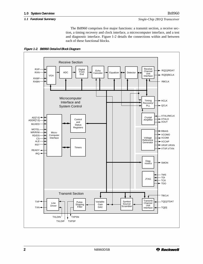
The Bt8960 comprises five major functions: a transmit section, a receive sec-tion, a timing recovery and clock interface, a microcomputer interface, and a testand diagnostic interface. Figure 1-2 details the connections within and betweeneach of these functional blocks.
Figure 1-2. Bt8960 Detailed Block Diagram
EchoCanceler
TimingRecovery/
CrystalAmplifier
Diag-nostics
JTAG
Receive Section
MicrocomputerInterface and
System Control
Transmit SectionTBCLK
MOTEL
ALECS
RD/DSWR/R/W
AD[7:0]
IRQ
RST
TXP
TXN
RQ[0]/BCLK
SMON
TMSTDITCKTDO
TQ[1]/TDAT
TQ[0]
VGA
PLL
VoltageReferenceGenerator
Pulse-Shaping
Filter
Variable-LineDriver
TXPSN
TXPSP
TXLDIN
TXLDIP
Controland
StatusRegisters
Timers
Micro-ComputerInterface
READY
ADDR[7:0]
RXPRXN
RXBPRXBN
MUXED
GainDAC
ADCDigitalFrontEnd
Equalizer Detector
ReceiveChannel
UnitInterface
RQ[1]/RDAT
RBCLK
HCLK
QCLK
XTALI/MCLKXTALOXOUT
RBIAS
VCOMOVCOMI
VCCAP
VRXP,VRXNVTXP,VTXN
TransmitChannel
UnitInterface
SymbolSource/
Scrambler
2 N8960DSB
1.0 System Overview
1.1 Functional Summary
Bt8960
Single-Chip 2B1Q Transceiver
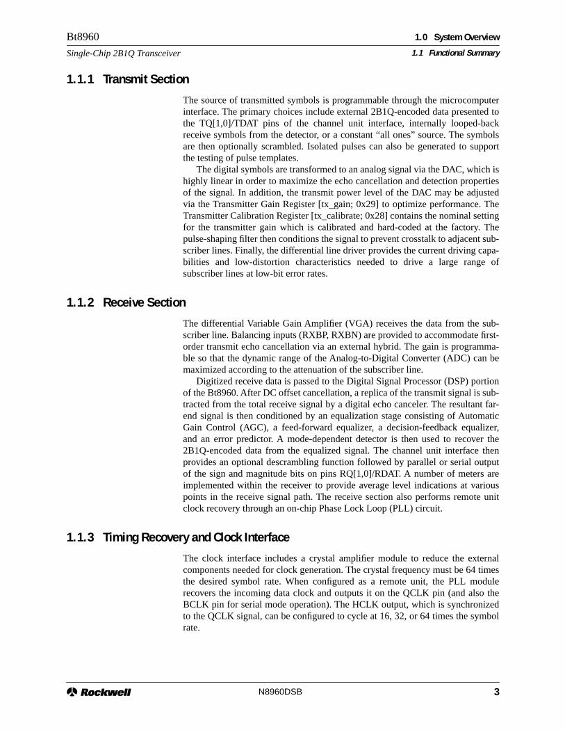
1.1.1 Transmit Section
The source of transmitted symbols is programmable through the microcomputerinterface. The primary choices include external 2B1Q-encoded data presented tothe TQ[1,0]/TDAT pins of the channel unit interface, internally looped-backreceive symbols from the detector, or a constant “all ones” source. The symbolsare then optionally scrambled. Isolated pulses can also be generated to supportthe testing of pulse templates.
The digital symbols are transformed to an analog signal via the DAC, which ishighly linear in order to maximize the echo cancellation and detection propertiesof the signal. In addition, the transmit power level of the DAC may be adjustedvia the Transmitter Gain Register [tx_gain; 0x29] to optimize performance. TheTransmitter Calibration Register [tx_calibrate; 0x28] contains the nominal settingfor the transmitter gain which is calibrated and hard-coded at the factory. Thepulse-shaping filter then conditions the signal to prevent crosstalk to adjacent sub-scriber lines. Finally, the differential line driver provides the current driving capa-bilities and low-distortion characteristics needed to drive a large range ofsubscriber lines at low-bit error rates.
1.1.2 Receive Section
The differential Variable Gain Amplifier (VGA) receives the data from the sub-scriber line. Balancing inputs (RXBP, RXBN) are provided to accommodate first-order transmit echo cancellation via an external hybrid. The gain is programma-ble so that the dynamic range of the Analog-to-Digital Converter (ADC) can bemaximized according to the attenuation of the subscriber line.
Digitized receive data is passed to the Digital Signal Processor (DSP) portionof the Bt8960. After DC offset cancellation, a replica of the transmit signal is sub-tracted from the total receive signal by a digital echo canceler. The resultant far-end signal is then conditioned by an equalization stage consisting of AutomaticGain Control (AGC), a feed-forward equalizer, a decision-feedback equalizer,and an error predictor. A mode-dependent detector is then used to recover the2B1Q-encoded data from the equalized signal. The channel unit interface thenprovides an optional descrambling function followed by parallel or serial outputof the sign and magnitude bits on pins RQ[1,0]/RDAT. A number of meters areimplemented within the receiver to provide average level indications at variouspoints in the receive signal path. The receive section also performs remote unitclock recovery through an on-chip Phase Lock Loop (PLL) circuit.
1.1.3 Timing Recovery and Clock Interface
The clock interface includes a crystal amplifier module to reduce the externalcomponents needed for clock generation. The crystal frequency must be 64 timesthe desired symbol rate. When configured as a remote unit, the PLL modulerecovers the incoming data clock and outputs it on the QCLK pin (and also theBCLK pin for serial mode operation). The HCLK output, which is synchronizedto the QCLK signal, can be configured to cycle at 16, 32, or 64 times the symbolrate.
3 N8960DSB

1.0 System Overview 1.1 Functional Summary
Bt8960
Single-Chip 2B1Q Transceiver
1.1.4 Microcomputer Interface
The Microcomputer Interface (MCI) provides access to a 256-byte address spacewithin the transceiver. A combination of direct and indirect addressing methodsare used to access all internal locations. The MCI is designed to interface withboth Intel- and Motorola-style processors with no additional glue logic. AMOTEL control pin is provided to configure the bus interface control/handshakelines to conform to common Motorola/Intel conventions. A MUXED control pinis provided to configure the bus interface address and data lines for multiplexed orindependent data/address bus operation. Little-endian data formatting (least sig-nificant byte of a multibyte word stored at the lowest byte-address location) isused in all cases, regardless of MOTEL pin selection. A READY control pin isprovided to support wait-state insertion. An Interrupt Request (IRQ) output pinsupports low-latency responses to time-critical events within the transceiver.
Eight 16-bit timers and ten measurement meters are integrated into the trans-ceiver. The timers support various metering functions within the receiver section,and off-load the external microcomputer from complex timing operations associ-ated with startup procedures. Control and monitoring access to the timers andmeters is provided through the microcomputer interface.
1.1.5 Test and Diagnostic Interface (JTAG)
The test and diagnostic interface comprises a test access port and a Serial MonitorOutput (SMON). The test access port conforms to IEEE Std 1149.1-1990, (IEEEStandard Test Access Port and Boundary Scan Architecture). Also referred to asJoint Test Action Group (JTAG), this interface provides direct serial access toeach of the transceiver’s I/O pins. This capability can be used during an in-circuitboard test to increase the testability and reduce the cost of the in-circuit test pro-cess.
The serial monitor output can be viewed as a real-time virtual probe for look-ing at the transceiver’s internal signals. The programmable signal source is shiftedout serially at 16 times the symbol rate. The majority of the receive signal path isaccessible through this output.
4 N8960DSB

1.0 System Overview
1.2 Applications
Bt8960
Single-Chip 2B1Q Transceiver
1.2 Applications
1.2.1 Voice/Data Pairgain
A well-established market exists for voice pairgain systems. These systems trans-port several simultaneous phone conversations over a single twisted pair. They areused by telecommunications service providers to maximize the utilization of theexisting copper plant, and allow it to provision many more telephone circuits thanpossible with ordinary 4 kHz analog transport.
The external interfaces of voice pairgain systems, at both the central office andremote ends, are analog POTS lines. Various carrier techniques exist to facilitatethe single-pair transmission such as: the Frequency Domain Multiplexed (FDM)systems and Time Domain Multiplexed (TDM) systems. In FDM systems, eachvoice channel is modulated by a successively higher carrier, therefore the com-posite transmission consists of several frequency bands. In TDM systems, thevoice data is digitized and sampled in a channel-multiplexed fashion. AlthoughFDM systems are currently fielded, recent trends are clearly toward TDM systemsdue to the inherent advantages associated with digital transmission.
Traditional 1 + 3, also called PCM4 voice pairgain systems, use a combina-tion of 2:1 ADPCM compression and basic rate ISDN U-interface devices totransport four voice conversations on one twisted pair. The disadvantage of thisscheme is that clear 64 kbps channel capacity is lost due to the ADPCM voicecompression algorithm. This may prevent high-speed facsimile transmissionsfrom being transported reliably. Regarding the Bt8960, an alternate way exists toimplement this type of voice pairgain equipment. A Bt8960-based system cantransport four or six clear 64 kbps channels on a single pair. Clear 64 kbps trans-port assures the transmission of any baud-rate facsimile or can be used to provi-sion special data services such as switched 56, clear 64, and frame relay.
Figure 1-3 shows the architecture of a PCM6 voice pairgain system. As illus-trated, six analog Subscriber Line Interface Cards (SLIC) are connected to a con-centrating framer. The function of this framer is to time-multiplex the PCM datafrom the SLICs, create a transport frame, and handle signaling information. Theoutput of the framer is then passed on to the Bt8960 for conversion into the 2B1Qcode suitable for long-reach transport over the loop plant.
5 N8960DSB

1.0 System Overview 1.2 Applications
Bt8960
Single-Chip 2B1Q Transceiver
1.2.2 Internet Connectivity Transport
The growth of the Internet has created a tremendous demand for additional band-width in the local loop. When existing loop facilities are used to provide connec-tivity to Internet servers, they are limited to the 128 kbps offered by Basic RateISDN (BRI) service. Although those same loops could be provisioned throughHDSL (for E1 or T1 transport rates), the tariff structure for these services putstheir bandwidth beyond the practical reach of most consumers. It is unlikely thatthe E1/T1 tariff structure will change soon since it still represents significantvalue for business customers using E1/T1 leased lines for corporate data andvoice exchange.
The 128 kbps rate offered by BRI is sufficient for the text and graphic contentof most of today's home pages. However, when motion, video, or interactivity areadded, the data rate required is increased to well over 300 kbps.
The advent of the Bt8960 creates an intermediate solution between BRI andE1/T1 which opens a host of low-cost, higher bandwidth possibilities. With theBt8960, local loops could be provisioned for data rates up to 384 kbps with low-cost hardware. In addition, the full ISDN 18,000 ft. carrier service area could beserved with a higher data rate. Enabling hardware could, for example, take theform of LAN extender equipment, and terminals for such equipment could havestandard Ethernet connections to routers, personal computers, or workstations.The terminals could also use the Bt8960 2B1Q transport mechanism for the localloop link to the central office or Internet server location.
By placing a SLIC in the terminal and reserving a 64 kbps channel for voicetransport, simultaneous data and voice service could be offered over a singletwisted pair. The extraordinary low power of the Bt8960 allows for customer siteequipment to be remotely powered, thereby guaranteeing lifeline POTS service inthe event of power loss at the customer site.
Figure 1-3. PCM6 Voice Pairgain Block Diagram
SLIC
SLIC
SLIC
SLIC
SLIC
SLIC
PCMFramer Bt8960
LocalLoop
6 N8960DSB

1.0 System Overview
1.2 Applications
Bt8960
Single-Chip 2B1Q Transceiver
1.2.3 ISDN Basic Rate Interface Concentrator
Since many telecommunications service providers are positioning BRI service asresidential Internet or telecommuter connectivity, the lack of installed copperpairs into the residence could be a serious limitation to the proliferation of the ser-vice. The Bt8960 solves this problem because it is capable of 416 kbps data rates.Thus, it enables the transport of two full BRI U-interface channels (4B + 2D) on asingle twisted pair.
Alternatively, a BRI service and two POTS lines can be provisioned over asingle twisted pair. Another possible combination is six B-channels with a consol-idated D-channel for the provisioning of three ISDN lines on a single twisted pair.Users of this equipment can include a small office with two computers, eachneeding BRI service, or a residence requiring a BRI line and two POTS lines. Theprimary advantage of (1 or 2 BRIs + 1 or 2 POTS) is there is no need for expen-sive digital phones and when a POTS function is used, the full BRI bandwidth fordata traffic is retained.
7 N8960DSB

1.0 System Overview 1.3 Pin Descriptions
Bt8960
Single-Chip 2B1Q Transceiver
1.3 Pin Descriptions
The Bt8960 is packaged in a 100-Pin Plastic Quad Flat Pack (PQFP). The pinassignments are shown in Figure 1-4. A listing of pin labels, numbers, and I/Oassignments is given in Table 1-1. Signal definitions are provided in Table 1-2.The coding used in the I/O column is: O = digital output, OA = analog output, OD= open-drain output, I = digital input, IA = analog input, and I/O = bidirectional.
Figure 1-4. Pin Diagram
23456789101112131415161718192021222324252627282930
7978777675747372717069686766656463626160595857565554
VDD1CS
RD/DSWR/R/W
ALEIRQ
READYAD[0]AD[1]AD[2]AD[3]AD[4]AD[5]AD[6]
DGNDDGNDVDD2AD[7]
MOTELMUXED
ADDR[7]ADDR[6]ADDR[5]ADDR[4]ADDR[3]ADDR[2]ADDR[1]ADDR[0]
SMONVDD1
RXBNRXBPRXNRXPAGNDAGNDTXNAGNDVAATXPTXLDINTXLDIPTXPSNTXPSPATEST2ATEST1VAAVAAAGNDVTXNVTXPVCCAPVCOMOVCOMIRBIASVAAVAAAGNDVRXNVRXP
DG
ND
DG
ND
VD
D2
RS
TH
CLK
XO
UT
DG
ND
VD
D1
XTA
LOX
TALI
/MC
LKV
DD
2D
GN
DD
TE
ST
1D
TE
ST
2D
TE
ST
3V
DD
1D
GN
DD
TE
ST
4A
GN
DA
GN
D
535251
801
DG
ND
DG
ND
VD
D2
TC
KT
MS
TD
IT
DO
DT
ES
T6
DT
ES
T5
TB
CLK
RB
CLK
RQ
[0]/B
CLK
RQ
[1]/R
DAT
QC
LKT
Q[0
]T
Q[1
]/TD
ATD
GN
DV
DD
1A
GN
DV
AA
Bt8960
100 99 98 97 96 95 94 93 92 91 90 89 88 87 86 85 84 83 82 81
31 32 33 34 35 36 37 38 39 40 41 42 43 44 45 46 47 48 49 50
8 N8960DSB

1.0 System Overview
1.3 Pin Descriptions
Bt8960
Single-Chip 2B1Q Transceiver
Table 1-1. Pin Descriptions
Pin Pin Label I/O Pin Pin Label I/O Pin Pin Label I/O Pin Pin Label I/O
1 VDD1 – 26 ADDR[2] I 51 VRXP OA 76 AGND –
2 CS I 27 ADDR[1] I 52 VRXN OA 77 RXP IA
3 RD/DS I 28 ADDR[0] I 53 AGND – 78 RXN IA
4 WR/R/W I 29 SMON O 54 VAA – 79 RXBP IA
5 ALE I 30 VDD1 – 55 VAA – 80 RXBN IA
6 IRQ OD 31 DGND – 56 RBIAS OA 81 VAA –
7 READY OD 32 DGND – 57 VCOMI OA 82 AGND –
8 AD[0] I/O 33 VDD2 – 58 VCOMO OA 83 VDD1 –
9 AD[1] I/O 34 RST I 59 VCCAP OA 84 DGND –
10 AD[2] I/O 35 HCLK O 60 VTXP OA 85 TQ[1]/TDAT I
11 AD[3] I/O 36 XOUT O 61 VTXN OA 86 TQ[0] I
12 AD[4] I/O 37 DGND – 62 AGND – 87 QCLK O
13 AD[5] I/O 38 VDD1 – 63 VAA – 88 RQ[1]/RDAT O
14 AD[6] I/O 39 XTALO O 64 VAA – 89 RQ[0]/BCLK O
15 DGND – 40 XTALI/MCLK I 65 ATEST1 IA 90 RBCLK I
16 DGND – 41 VDD2 – 66 ATEST2 IA 91 TBCLK I
17 VDD2 – 42 DGND – 67 TXPSP OA 92 DTEST5 I
18 AD[7] I/O 43 DTEST1 I 68 TXPSN OA 93 DTEST6 I
19 MOTEL I 44 DTEST2 I 69 TXLDIP IA 94 TDO O
20 MUXED I 45 DTEST3 I 70 TXLDIN IA 95 TDI I
21 ADDR[7] I 46 VDD1 – 71 TXP OA 96 TMS I
22 ADDR[6] I 47 DGND – 72 VAA – 97 TCK I
23 ADDR[5] I 48 DTEST4 I 73 AGND – 98 VDD2 –
24 ADDR[4] I 49 AGND – 74 TXN OA 99 DGND –
25 ADDR[3] I 50 AGND – 75 AGND – 100 DGND –
9 N8960DSB

1.0 System Overview 1.3 Pin Descriptions
Bt8960
Single-Chip 2B1Q Transceiver
Table 1-2. Hardware Signal Definitions (1 of 4)
Pin Label Signal Name I/O Definition
Microcomputer Interface (MCI)
MOTEL Motorola/Intel I Selects between Motorola and Intel handshake conventions for the RD/DS and WR/R/W signals.
MOTEL = 1 for Motorola protocol: DS, R/WMOTEL = 0 for Intel protocol: RD, WR
ALE Address Latch Enable
I Falling-edge-sensitive input. The value of AD[7:0] when MUXED = 1, or ADDR[7:0] when MUXED = 0, is internally latched on the falling edge of ALE.
CS Chip Select I Active-low input used to enable read/write operations on the Microcomputer Interface (MCI).
RD/DS Read/Data Strobe I Bimodal input for controlling read/write access on the MCI. When MOTEL = 1 and CS = 0, RD/DS behaves as an active-low data strobe
DS. Internal data is output on AD[7:0] when DS = 0 and R/W = 1. External data is internally latched from AD[7:0] on the rising edge of DS when R/W = 0.
When MOTEL = 0 and CS = 0, RD/DS behaves as an active-low read strobe RD. Internal data is output on AD[7:0] when RD = 0. Write operations are not controlled by RD in this mode.
WR / R/W Write/Read/Write
I Bimodal input for controlling read/write access on the MCI. When MOTEL = 1 and CS = 0, WR/R/W behaves as a read/write select line
R/W. Internal data is output on AD[7:0] when DS = 0 and R/W = 1. External data is internally latched from AD[7:0] on the rising edge of DS when R/W = 0.
When MOTEL = 0 and CS = 0, WR/R/W behaves as an active-low write strobe WR. External data is internally latched from AD[7:0] on the rising edge of WR. Read operations are not controlled by WR in this mode.
AD[7:0] Address-Data[7:0]
I/O 8-bit bidirectional multiplexed address-data bus. AD[7] = MSB, AD[0] = LSB. Usage is controlled using the MUXED signal as defined below.
ADDR[7:0] Address Bus[7:0](Not Multiplexed)
I Provides a glueless interface to microcomputers with separate address and data buses. ADDR[7] = MSB, ADDR[0] = LSB. Usage is controlled using the MUXED signal.
MUXED Addressing Mode Select
I Controls the MCI addressing mode.When MUXED = 1, the MCI uses AD[7:0] as a multiplexed signal for address
and data (typical of Intel processors).When MUXED = 0, the MCI uses ADDR[7:0] as the address input and
AD[7:0] for data only (typical of Motorola processors).
READY Ready OD Active-low, open-drain output that indicates that the MCI is ready to transfer data. Can be used to signal the microcomputer to insert wait states.
IRQ Interrupt Request OD Active-low, open-drain output that indicates requests for interrupt. Asserted whenever at least one unmasked interrupt flag is set. Remains inactive whenever no unmasked interrupt flags are present.
RST Reset I Asynchronous, active-low, level-sensitive input that places the transceiver in an inactive state by setting the power-down mode bit of the Global Modes and Sta-tus Register [global_modes; 0x00], and zeroing the clk_freq[1,0] bits of the PLL Modes Register [pll_modes; 0x22], and the hclk_freq[1,0] bits of the Serial Monitor Source Select Register [serial_monitor_source; 0x01]. All RAM con-tents are lost. Does not affect the state of the test access port which is reset automatically at power-up only.
10 N8960DSB

1.0 System Overview
1.3 Pin Descriptions
Bt8960
Single-Chip 2B1Q Transceiver
Channel Unit Interface
RQ[1]/RDAT
RQ[0]/ BCLK
Receive Quat 1/ Receive Data
Receive Quat 0/ Bit Clock
O
O
RQ[1]/RDAT and RQ[0]/BCLK are bimodal outputs that represent the sign and magnitude bits of the received quaternary output symbol in parallel channel unit modes (RQ[1], RQ[0]), and the serial-data and bit-clock outputs in serial chan-nel unit modes (RDAT, BCLK). Behavior of these outputs is configurable through the Channel Unit Interface Modes Register [CU_interface_modes; 0x06] for par-allel master, parallel slave, serial magnitude-bit-first and serial sign-bit-first operations.
For parallel mode operation:
RQ[1] = Sign bit outputRQ[0] = Magnitude bit output
Both outputs are updated at the symbol rate on the rising edge of QCLK (master mode) or the rising/falling edge (programmable) of RBCLK (slave mode).
For serial mode operation:
RDAT = Serial quaternary data outputBCLK = Bit-rate (two times symbol rate) clock output RDAT is updated at the bit rate on the rising edge of BCLK
TQ[1]/ TDAT
TQ[0]
Transmit Quat 1/ Transmit Data
Transmit Quat 0
I
I
TQ[1]/TDAT and TQ[0] are bimodal inputs that represent the sign and magnitude bits of the quaternary input symbol to be transmitted in parallel channel unit modes (TQ[1], TQ[0]), and the serial data input in serial channel unit modes (TDAT). Interpretation of these inputs is configurable through the Channel Unit Interface Modes Register [CU_Interface_modes; 0x06] for parallel master, par-allel slave, serial magnitude-bit-first and serial sign-bit-first operations.
For parallel mode operation:
TQ[1] = Sign bit inputTQ[0] = Magnitude bit input
Both inputs are sampled at the symbol rate on the falling edge of QCLK (mas-ter mode) or the rising/falling edge (programmable) of TBCLK (slave mode).
For serial mode operation:
TDAT = Serial quaternary data inputTQ0 = Don’t care (tie or pull up to supply rail)
TDAT is sampled at the bit rate (two times the symbol rate) on the falling edge of BCLK.
QCLK Quaternary Clock O Runs at the symbol rate. It defines the data on the TQ and RQ interfaces. QCLK is also used to frame transmit/receive quats in serial mode.
TBCLK Transmit Baud-Rate Clock
I Functions as the transmit baud-rate clock input. It must be frequency locked to QCLK. This input is used only when the channel unit interface is in parallel slave mode. If it is unused, it should be tied to VDD2 or DGND.
RBCLK Receive Baud-Rate Clock
I Functions as the receive baud-rate clock input. It must be frequency locked to QCLK. This input is used only when the channel unit interface is in parallel slave mode. If it is unused, it should be tied to VDD2 or DGND.
Table 1-2. Hardware Signal Definitions (2 of 4)
Pin Label Signal Name I/O Definition
11 N8960DSB
1.0 System Overview 1.3 Pin Descriptions
Bt8960
Single-Chip 2B1Q Transceiver
Analog Transmit Interface
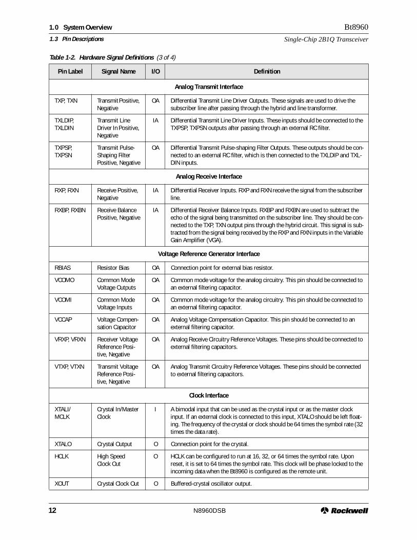
TXP, TXN Transmit Positive, Negative
OA Differential Transmit Line Driver Outputs. These signals are used to drive the subscriber line after passing through the hybrid and line transformer.
TXLDIP, TXLDIN
Transmit Line Driver In Positive, Negative
IA Differential Transmit Line Driver Inputs. These inputs should be connected to the TXPSP, TXPSN outputs after passing through an external RC filter.
TXPSP, TXPSN
Transmit Pulse- Shaping Filter Positive, Negative
OA Differential Transmit Pulse-shaping Filter Outputs. These outputs should be con-nected to an external RC filter, which is then connected to the TXLDIP and TXL-DIN inputs.
Analog Receive Interface
RXP, RXN Receive Positive, Negative
IA Differential Receiver Inputs. RXP and RXN receive the signal from the subscriber line.
RXBP, RXBN Receive Balance Positive, Negative
IA Differential Receiver Balance Inputs. RXBP and RXBN are used to subtract the echo of the signal being transmitted on the subscriber line. They should be con-nected to the TXP, TXN output pins through the hybrid circuit. This signal is sub-tracted from the signal being received by the RXP and RXN inputs in the Variable Gain Amplifier (VGA).
Voltage Reference Generator Interface
RBIAS Resistor Bias OA Connection point for external bias resistor.
VCOMO Common Mode Voltage Outputs
OA Common mode voltage for the analog circuitry. This pin should be connected to an external filtering capacitor.
VCOMI Common Mode Voltage Inputs
OA Common mode voltage for the analog circuitry. This pin should be connected to an external filtering capacitor.
VCCAP Voltage Compen-sation Capacitor
OA Analog Voltage Compensation Capacitor. This pin should be connected to an external filtering capacitor.
VRXP, VRXN Receiver Voltage Reference Posi-tive, Negative
OA Analog Receive Circuitry Reference Voltages. These pins should be connected to external filtering capacitors.
VTXP, VTXN Transmit Voltage Reference Posi-tive, Negative
OA Analog Transmit Circuitry Reference Voltages. These pins should be connected to external filtering capacitors.
Clock Interface
XTALI/ MCLK
Crystal In/Master Clock
I A bimodal input that can be used as the crystal input or as the master clock input. If an external clock is connected to this input, XTALO should be left float-ing. The frequency of the crystal or clock should be 64 times the symbol rate (32 times the data rate).
XTALO Crystal Output O Connection point for the crystal.
HCLK High Speed Clock Out
O HCLK can be configured to run at 16, 32, or 64 times the symbol rate. Upon reset, it is set to 64 times the symbol rate. This clock will be phase locked to the incoming data when the Bt8960 is configured as the remote unit.
XOUT Crystal Clock Out O Buffered-crystal oscillator output.
Table 1-2. Hardware Signal Definitions (3 of 4)
Pin Label Signal Name I/O Definition
12 N8960DSB

1.0 System Overview
1.3 Pin Descriptions
Bt8960
Single-Chip 2B1Q Transceiver
Test and Diagnostic Interface
TDI JTAG Test Data Input
I JTAG test data input per IEEE Std 1149.1-1990. Used for loading all serial instructions and data into internal test logic. Sampled on the rising edge of TCK. TDI can be left unconnected if it is not being used because it is pulled-up inter-nally.
TMS JTAG Test Mode Select
I JTAG test mode select input per IEEE Std 1149.1-1990. Internally pulled-up input signal used to control the test-logic state machine. Sampled on the rising edge of TCK. TMS can be left unconnected if it is not being used because it is pulled-up internally.
TDO JTAG Test Data Output
O JTAG test data output per IEEE Std 1149.1-1990. Three-state output used for reading all serial configuration and test data from internal test logic. Updated on the falling edge of TCK.
TCK JTAG Test Clock Input
I JTAG test clock input per IEEE Std 1149.1-1990. Used for all test interface and internal test logic operations. If unused, TCK should be pulled low.
SMON Serial Monitor O Serial data output used for real-time monitoring of internal signal-path registers. The source register is selected through the Serial Monitor Source Select Regis-ter [serial_monitor_source; 0x01]. 16-bit words are shifted out, LSB first, at 16 times the symbol rate. The rising edge of QCLK defines the start Least Signifi-cant Bit (LSB) of each word. The output is updated on the rising edge of an inter-nal clock running at 16 times QCLK.
DTEST[1:4] Digital Tests 1–4 I Active-high test inputs used by Rockwell to enable internal test modes. These inputs should be tied to digital ground (DGND).
DTEST[5, 6] Digital Test 5, 6 I Active-low test inputs used by Rockwell to enable internal test modes. These inputs should be tied to the I/O buffer power supply (VDD2).
ATEST[1,2] Analog Test 1, 2 IA Analog test inputs used by Rockwell for internal test modes. These inputs should be left floating (No Connect, NC).
Power and Ground
VDD1 Core Logic PowerSupply
– Dedicated supply pins powering the digital core logic functions.
VDD2 I/O Buffer Power Supply
– Dedicated supply pins powering the digital I/O buffers.
DGND Digital Ground – Dedicated ground pins for the digital circuitry. Must be held at same potential as AGND.
VAA Analog Power Supply
– Dedicated supply pins powering the analog circuitry.
AGND Analog Ground – Dedicated ground pins for the analog circuitry. Must be held at the same poten-tial as DGND.
Table 1-2. Hardware Signal Definitions (4 of 4)
Pin Label Signal Name I/O Definition
13 N8960DSB
1.0 System Overview 1.3 Pin Descriptions
Bt8960
Single-Chip 2B1Q Transceiver
14 N8960DSB

2.0 Functional Description
2.1 Transmit Section
The transmit section is illustrated in Figure 2-1. It comprises four major func-tions: a symbol source selector/scrambler, a variable gain digital-to-analog con-verter (DAC), a pulse-shaping filter, and a line driver.
Figure 2-1. Transmit Section Block Diagram
TransmitChannel Unit
InterfaceSymbol
Variable-Gain LineDriver
ControlRegisters
ExternalRC Filter
TQ[1,0] TXPTXN
Isolated PulsesDetector Loopback
Ones (1s)
Source/Scrambler
Pulse-Shaping
FilterDAC
15 N8960DSB

2.0 Functional Description 2.1 Transmit Section
Bt8960
Single-Chip 2B1Q Transceiver
2.1.1 Symbol Source Selector/Scrambler
The input source selector/scrambler can be configured through the TransmitterModes Register [transmitter_modes; 0x0B] data_source [2:0] bits to select thesource of the data to be transmitted and determine whether or not the data isscrambled. The symbol source selector/scrambler modes are specified in Table 2-1.
Table 2-1. Symbol Source Selector/Scrambler Modes
data_source[2:0] Symbol Source Selector/Scrambler Mode
000 Isolated pulse. Level selected by isolated_pulse[1,0]. The meter timer must be enabled and in the con-tinuous mode. The pulse repetition interval is determined by the meter-timer-countdown interval.
001 Four-level scrambled detector loopback. Sign and magnitude bits from the receiver detector are scram-bled and looped back to the transmitter. Feedback polynomial determined by the htur_lfsr control bit.
010 Four-level unscrambled data. Transmits the four-level (2B1Q) sign and magnitude bits from the transmit channel unit.
011 Four-level scrambled ones. Transmits a scrambled, constant high-logic level as a four-level (2B1Q) sig-nal. Feedback polynomial determined by the htur_lfsr control bit.
100 Reserved.
101 Four-level scrambled data. Scrambles and transmits the four-level (2B1Q) sign and magnitude bits from the channel unit transmit interface. Feedback polynomial determined by the htur_lfsr control bit.
110 Two-level unscrambled data. Constantly forces the magnitude bit from the transmit channel unit inter-face to a logic zero, and transmits the resulting two-level signal (as determined by the sign bit) without scrambling. Valid output levels limited to +3, –3.
111 Two-level scrambled ones. Transmits a scrambled, constant high-logic level, as a two-level signal. Feed-back polynomial determined by the htur_lfsr control bit. Scrambler is run at the symbol rate (half-bit rate) to produce the sign bit of the transmitted signal while the magnitude bit is sourced with a constant logic zero. Valid output levels limited to +3, –3.
16 N8960DSB
2.0 Functional Description
2.1 Transmit Section
Bt8960
Single-Chip 2B1Q Transceiver
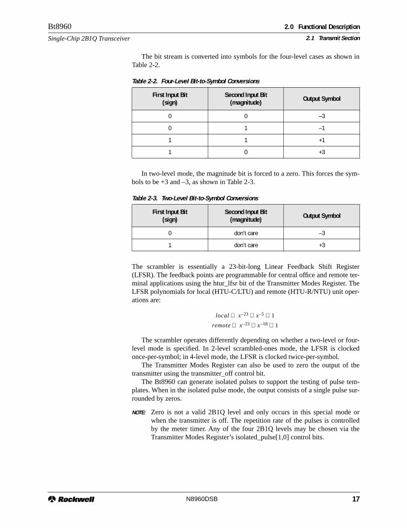
The bit stream is converted into symbols for the four-level cases as shown inTable 2-2.
In two-level mode, the magnitude bit is forced to a zero. This forces the sym-bols to be +3 and –3, as shown in Table 2-3.
The scrambler is essentially a 23-bit-long Linear Feedback Shift Register(LFSR). The feedback points are programmable for central office and remote ter-minal applications using the htur_lfsr bit of the Transmitter Modes Register. TheLFSR polynomials for local (HTU-C/LTU) and remote (HTU-R/NTU) unit oper-ations are:
The scrambler operates differently depending on whether a two-level or four-level mode is specified. In 2-level scrambled-ones mode, the LFSR is clockedonce-per-symbol; in 4-level mode, the LFSR is clocked twice-per-symbol.
The Transmitter Modes Register can also be used to zero the output of thetransmitter using the transmitter_off control bit.
The Bt8960 can generate isolated pulses to support the testing of pulse tem-plates. When in the isolated pulse mode, the output consists of a single pulse sur-rounded by zeros.
NOTE: Zero is not a valid 2B1Q level and only occurs in this special mode orwhen the transmitter is off. The repetition rate of the pulses is controlledby the meter timer. Any of the four 2B1Q levels may be chosen via theTransmitter Modes Register’s isolated_pulse[1,0] control bits.
Table 2-2. Four-Level Bit-to-Symbol Conversions
First Input Bit (sign)
Second Input Bit (magnitude) Output Symbol
0 0 –3
0 1 –1
1 1 +1
1 0 +3
Table 2-3. Two-Level Bit-to-Symbol Conversions
First Input Bit (sign)
Second Input Bit (magnitude) Output Symbol
0 don’t care –3
1 don’t care +3
local x 23– x 5– 1⊕ ⊕⇒
remote x 23– x 18– 1⊕ ⊕⇒
17 N8960DSB

2.0 Functional Description 2.1 Transmit Section
Bt8960
Single-Chip 2B1Q Transceiver
2.1.2 Variable Gain Digital-to-Analog Converter
A four-level Digital-to-Analog Converter (DAC) is integrated into the Bt8960 toaccurately convert the output of the symbol source to analog form. The normal-ized values of these four analog levels are: +3, +1, –1 and –3. Each represents asymbol or quat.
To provide precise adjustment of the transmitted power, the level of the DACmay be adjusted. The Transmitter Gain Register [tx_gain; 0x29] sets the level.
During the manufacturing of the Bt8960, one source of variation in the trans-mitter levels is process variations. The Transmitter Calibration Register[tx_calibrate; 0x28] contains a read-only value which nulls this variation. Thevalue of this register is determined for each Bt8960 device during production test-ing. Upon initialization, the Transmitter Gain Register should be loaded based onthe Transmitter Calibration Register.
If there are other sources of transmit power variation (e.g., a nonstandardhybrid or attenuative lightening protection), the transmitter gain must be adjustedto include these affects.
2.1.3 Pulse-Shaping Filter
The pulse-shaping filter filters the quats output from the variable-gain DAC. Thisfilter, when combined with other filtering in the signal path, produces a transmit-ted signal on the line that meets the power spectral density, transmitted power,and pulse-shaping requirements, as specified in the Electrical Specifications sec-tion of this datasheet.
2.1.4 Line Driver
The line driver buffers the output of the pulse-shaping filter to drive diverse loads.The output of the line driver is differential.
18 N8960DSB
2.0 Functional Description
2.2 Receive Section
Bt8960
Single-Chip 2B1Q Transceiver
2.2 Receive Section
Like the transmit section, the receive section consists of both analog and digitalcircuitry. The VGA provides the interface to the analog signals received from theline and the hybrid. The Analog-to-Digital Converter (ADC) then digitizes theanalog signal so it can be further processed in the digital signal Processing (DSP)section of the receiver. The receiver DSP section includes: front-end processing,echo cancellation, equalization, and symbol detection.
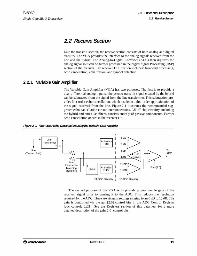
2.2.1 Variable Gain Amplifier
The Variable Gain Amplifier (VGA) has two purposes. The first is to provide adual-differential analog input so the pseudo-transmit signal created by the hybridcan be subtracted from the signal from the line transformer. This subtraction pro-vides first-order echo cancellation, which results in a first-order approximation ofthe signal received from the line. Figure 2-1 illustrates the recommended sug-gested echo-cancellation circuit interconnections. All off-chip circuitry, includingthe hybrid and anti-alias filters, consists entirely of passive components. Furtherecho cancellation occurs in the receiver DSP.
The second purpose of the VGA is to provide programmable gain of thereceived signal prior to passing it to the ADC. This reduces the resolutionrequired for the ADC. There are six gain settings ranging from 0 dB to 15 dB. Thegain is controlled via the gain[2:0] control bits in the ADC Control Register[adc_control; 0x21]. See the Registers section of this datasheet for a moredetailed description of the gain[2:0] control bits.
Figure 2-2. First-Order Echo Cancellation Using the Variable Gain Amplifier
RXP
RXN
RXBP
RXBN
TXP
TXN
Line(Twisted Pair)
ToADC
On-Chip CircuitryOff-Chip Circuitry
LineImpedanceMatching Gain[2:0]
Anti-AliasFilter
Hybrid–
+ Anti-aliasFilter
+
–
+
–
+
–
+–
LineDriver
LineTransformer
+
–
Resistors
19 N8960DSB

2.0 Functional Description 2.2 Receive Section
Bt8960
Single-Chip 2B1Q Transceiver
2.2.2 Analog-to-Digital Converter
The ADC provides 16 bits of resolution. The analog input from the variable gainamplifier is converted into digital data and output at the symbol rate.
2.2.3 Digital Signal Processor
The Digital Signal Processor (DSP) includes five Least Mean Squared (LMS) fil-ters: an Echo Canceller (EC), a Digital Automatic Gain Controller (DAGC), aFeed Forward Equalizer (FFE), an Error Predictor (EP), and a Decision FeedbackEqualizer (DFE). These filters are used to equalize the received signal so that thesymbols transmitted from the far-end can be reliably recovered. The DSP usessymbol rate sampling for all processing functions. Their interconnections andrelationships to the digital front-end and the detector are illustrated in Figure 2-3.
Figure 2-3. Receiver Digital Signal Processing
DigitalFront-End
ChannelUnit
Interface
Echo Canceller
TransmitSymbol
Equalizer
DFE
Detector
LEC
DAGC FFE
NEC
EP
PKD
Slicer–– ––
–
–
20 N8960DSB

2.0 Functional Description
2.2 Receive Section
Bt8960
Single-Chip 2B1Q Transceiver
2.2.3.1 DigitalFront-End
Prior to the main signal processing, the input signal must be adjusted for any DCoffset. The front-end module also monitors the input signal level, which includesmeasuring DC and AC input signal levels, detecting and counting overflows, anddetecting alarms based on the far-end signal level. Figure 2-4 summarizes the fea-tures of the digital front-end module.
Figure 2-4. Digital Front-End Block Diagram
Echo-FreeSignal
from NEC
DC Offsetfrom MCI
Accumulator
ResultRegister
Far-EndLevel Meter
Comparator
Comparator
Far-EndAlarms
High Thresholdfrom MCI
Low Thresholdfrom MCI
high_felmInterrupt
low_felmInterrupt
ResultRegister
Accumulator
DC LevelMeter
Accumulator
Absolute
ResultRegister
Signal LevelMeter
ADC Datar, To EC+
–
OverflowDetector
Counter
ResultRegister
Overflow Monitor
Overflow
AbsoluteValue
Value
21 N8960DSB

2.0 Functional Description 2.2 Receive Section
Bt8960
Single-Chip 2B1Q Transceiver
2.2.3.2 OffsetAdjustment
A nonzero DC level on the input can be corrected by a DC offset value[dc_offset_low, dc_offset_high; 0x26, 0x27] which is subtracted from the input.The DC offset is a 16-bit number and is programmed via the microcomputerinterface.
2.2.3.3 DC Level Meter The DC level meter provides the monitoring needed for adaptive offset compen-sation. The offset-adjusted input signal is accumulated over the meter timer inter-val [meter_low, meter_high; 0x18, 0x19]. The 16 MSBs are placed into the DCLevel Meter Registers [dc_meter_low, dc_meter_high; 0x44, 0x45].
2.2.3.4 Signal LevelMeter
The signal level meter provides the monitoring needed for adjusting the analoggain circuit located prior to the ADC. This value is accumulated over the metertimer interval [meter_low, meter_high; 0x18, 0x19]. The 16 MSBs are placed inthe Signal Level Meter Registers [slm_low, slm_high; 1; 0x46, 0x47].
2.2.3.5 OverflowDetection
and Monitoring
The overflow sensor detects ADC overflows. The overflow monitor counts thenumber of overflows, as indicated by the overflow sensor during the meter timerinterval [meter_low, meter_high; 0x18, 0x19]. The counter is limited to 8 bits. Inthe case of 256 or more overflows during the measurement interval, the counterwill hold at 255. The counter is loaded into the Overflow Meter Register[overflow_meter; 0x42] at the end of each measurement interval.
2.2.3.6 Far-End LevelMeter
The far-end level meter monitors the output of the echo canceler. Since the echocanceler output had the echo of the transmitted signal subtracted from it, it iscalled the far-end signal. This value is accumulated over the meter timer interval[meter_low, meter_high; 0x18, 0x19]. The 16 MSBs are placed into the Far-EndLevel Meter Register [felm_low, felm_high; 0x48, 0x49].
2.2.3.7 Far-End LevelAlarm
The result of the far-end level meter is compared to two thresholds. Whenexceeded, an interrupt is sent to the microcomputer interface, if enabled. Thethreshold is determined by the value in the Far-End High Alarm Threshold Regis-ters [far_end_high_alarm_th_low, far_end_high_alarm_th_high; 0x30, 0x31] andthe Far-End Low Alarm Threshold Registers [far_end_low_alarm_th_low,far_end_low_alarm_th_high; 0x32, 0x33].
The interrupts high_felm and low_felm, are bits 2 and 1, respectively of theIRQ Source Register [irq_source; 0x05]. The interrupts high_felm and low_felm,can be masked by writing a one to bits 2 and 1, respectively of the Interrupt MaskRegister High [mask_high_reg; 0x03].
22 N8960DSB
2.0 Functional Description
2.2 Receive Section
Bt8960
Single-Chip 2B1Q Transceiver
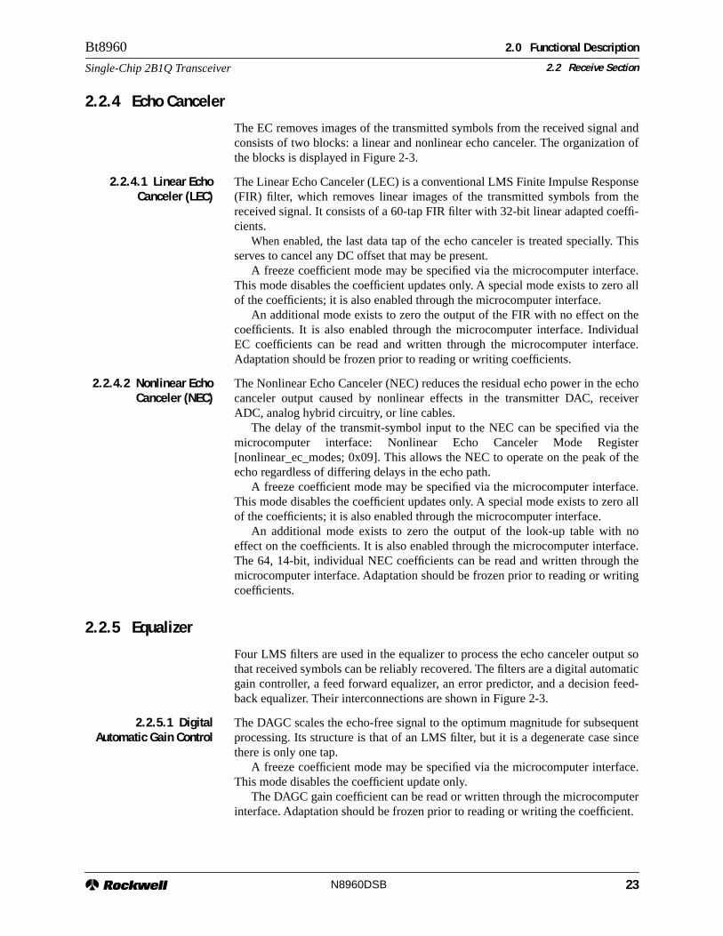
2.2.4 Echo Canceler
The EC removes images of the transmitted symbols from the received signal andconsists of two blocks: a linear and nonlinear echo canceler. The organization ofthe blocks is displayed in Figure 2-3.
2.2.4.1 Linear EchoCanceler (LEC)
The Linear Echo Canceler (LEC) is a conventional LMS Finite Impulse Response(FIR) filter, which removes linear images of the transmitted symbols from thereceived signal. It consists of a 60-tap FIR filter with 32-bit linear adapted coeffi-cients.
When enabled, the last data tap of the echo canceler is treated specially. Thisserves to cancel any DC offset that may be present.
A freeze coefficient mode may be specified via the microcomputer interface.This mode disables the coefficient updates only. A special mode exists to zero allof the coefficients; it is also enabled through the microcomputer interface.
An additional mode exists to zero the output of the FIR with no effect on thecoefficients. It is also enabled through the microcomputer interface. IndividualEC coefficients can be read and written through the microcomputer interface.Adaptation should be frozen prior to reading or writing coefficients.
2.2.4.2 Nonlinear EchoCanceler (NEC)
The Nonlinear Echo Canceler (NEC) reduces the residual echo power in the echocanceler output caused by nonlinear effects in the transmitter DAC, receiverADC, analog hybrid circuitry, or line cables.
The delay of the transmit-symbol input to the NEC can be specified via themicrocomputer interface: Nonlinear Echo Canceler Mode Register[nonlinear_ec_modes; 0x09]. This allows the NEC to operate on the peak of theecho regardless of differing delays in the echo path.
A freeze coefficient mode may be specified via the microcomputer interface.This mode disables the coefficient updates only. A special mode exists to zero allof the coefficients; it is also enabled through the microcomputer interface.
An additional mode exists to zero the output of the look-up table with noeffect on the coefficients. It is also enabled through the microcomputer interface.The 64, 14-bit, individual NEC coefficients can be read and written through themicrocomputer interface. Adaptation should be frozen prior to reading or writingcoefficients.
2.2.5 Equalizer
Four LMS filters are used in the equalizer to process the echo canceler output sothat received symbols can be reliably recovered. The filters are a digital automaticgain controller, a feed forward equalizer, an error predictor, and a decision feed-back equalizer. Their interconnections are shown in Figure 2-3.
2.2.5.1 DigitalAutomatic Gain Control
The DAGC scales the echo-free signal to the optimum magnitude for subsequentprocessing. Its structure is that of an LMS filter, but it is a degenerate case sincethere is only one tap.
A freeze coefficient mode may be specified via the microcomputer interface.This mode disables the coefficient update only.
The DAGC gain coefficient can be read or written through the microcomputerinterface. Adaptation should be frozen prior to reading or writing the coefficient.
23 N8960DSB

2.0 Functional Description 2.2 Receive Section
Bt8960
Single-Chip 2B1Q Transceiver
2.2.5.2 Feed ForwardEqualizer (FFE)
The Feed Forward Equalizer (FFE) removes precursors from the received signal.The FFE may be operated in a special adapt last mode. In this mode, which isuseful during startup, only the last coefficient is updated. The last coefficient isthe one which is multiplied with the oldest data sample, (sample #7).
A freeze coefficient mode may be specified via the microcomputer interface.This mode disables the coefficient updates only. A special mode exists to zero allof the coefficients. It is also enabled through the microcomputer interface. Indi-vidual FFE coefficients can be read and written through the microcomputer inter-face. Adaptation should be frozen prior to reading or writing coefficients.
2.2.5.3 ErrorPredictor (EP)
The Error Predictor (EP) improves the performance of the equalizer by prognosti-cating errors before they occur. A freeze coefficient mode may be specified viathe microcomputer interface. This mode disables the coefficient updates only. Aspecial mode exists to zero all of the coefficients; it is also enabled through themicrocomputer interface. Individual EP coefficients can be read and writtenthrough the microcomputer interface. Adaptation should be frozen prior to read-ing or writing coefficients.
2.2.5.4 DecisionFeedback Equalizer
(DFE)
The Decision Feedback Equalizer (DFE) removes postcursors from the receivedsignal. A freeze coefficient mode may be specified via the microcomputer inter-face. This mode disables the coefficient updates only. A zero coefficients modeexists to zero all of the coefficients; it is also enabled through the microcomputerinterface. A zero filter output mode exists to zero the output of the FIR with noeffect on the coefficients. It is also enabled through the microcomputer interface.Individual DFE coefficients can be read and written through the microcomputerinterface. Adaptation should be frozen prior to reading or writing coefficients.
2.2.5.5 Microcoding The DAGC, FFE, and EP filters are implemented using an internal micropro-grammable Digital Signal Processor (DSP) optimized for LMS filters. InternalDSP micro-instructions are stored in an on-chip RAM. This microcode RAM isloaded after powerup through the microcomputer interface when the transceiver isinitialized.
2.2.6 Detector
The detector converts the equalized received signal into a 2B1Q symbol and pro-duces two error signals used in adapting the receiver equalizers. The signal detec-tion uses two sub-blocks, a slicer, and a peak detector. Additionally, the detectorcontains a scrambler and Bit Error Rate (BER) meter for use during the startupsequence.
2.2.6.1 Slicer The slicer thresholds the equalized signal to produce a 2B1Q symbol. The inputto the slicer is the FFE output minus the DFE and EP outputs.
The slicer can operate in two modes: two-level and four-level. In the two-levelmode, used during the part of startup when the only transmitted symbols are +3 or–3, the slicer threshold is set at zero.
When in four-level mode, the cursor level is specified via the microcomputerinterface. It is a 16-bit, 2’s complement number, but must be positive and lessthan 0x2AAA for proper operation.
24 N8960DSB
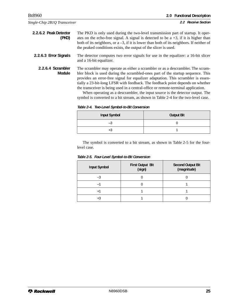
2.0 Functional Description
2.2 Receive Section
Bt8960
Single-Chip 2B1Q Transceiver
2.2.6.2 Peak Detector(PKD)
The PKD is only used during the two-level transmission part of startup. It oper-ates on the echo-free signal. A signal is detected to be a +3, if it is higher thanboth of its neighbors, or a –3, if it is lower than both of its neighbors. If neither ofthe peaked conditions exists, the output of the slicer is used.
2.2.6.3 Error Signals The detector computes two error signals for use in the equalizer: a 16-bit slicerand a 16-bit equalizer.
2.2.6.4 ScramblerModule
The scrambler may operate as either a scrambler or as a descrambler. The scram-bler block is used during the scrambled-ones part of the startup sequence. Thisprovides an error-free signal for equalizer adaptation. This scrambler is essen-tially a 23-bit-long LFSR with feedback. The feedback point depends on whetherthe transceiver is being used in a central-office or remote-terminal application.
When operating as a descrambler, the input source is the detector output. Thesymbol is converted to a bit stream, as shown in Table 2-4 for the two-level case.
The symbol is converted to a bit stream, as shown in Table 2-5 for the four-level case.
Table 2-4. Two-Level Symbol-to-Bit Conversion
Input Symbol Output Bit
–3 0
+3 1
Table 2-5. Four-Level Symbol-to-Bit Conversion
Input Symbol First Output Bit (sign)
Second Output Bit (magnitude)
–3 0 0
–1 0 1
+1 1 1
+3 1 0
25 N8960DSB
2.0 Functional Description 2.2 Receive Section
Bt8960
Single-Chip 2B1Q Transceiver
The LFSR operates in the same way in both cases, except in the two-level caseit is clocked once-per-symbol and in the four-level case it is clocked twice-per-symbol.
When operating as a scrambler, the LFSR must first be locked to the far-endsource. Once locked, it is then able to replicate the far-end input sequence, whenits input is held at all ones. The locking sequence is controlled internally, initiatedthrough the microcomputer interface by setting the lfsr_lock bit of thedetector_modes register. The locking sequence consists of the following foursteps:
1. Operate the LFSR as a descrambler for 23 bits.2. Operate the LFSR as a scrambler for 127 bits. The sync detector is active
during this period. 3. Go to Step 1 if synchronization was not achieved, otherwise continue to
Step 4.4. Send an interrupt to the microcomputer, if unmasked, indicating successful
locking and continue operating as a scrambler.
The sequence continues until the lfsr_lock control bit is cleared by the micro-computer.
2.2.6.5 Sync Detector The sync detector compares the output of the scrambler with the output of thesymbol detector. The number of equivalent bits is accumulated for 128 compari-sons. The result is then compared to a Scrambler Synchronization Threshold Reg-ister [scr_sync_th; 0x2E], lock is declared, and the sync bit of the irq_sourceregister is set if the count is greater than the threshold. For a count less than orequal to the threshold, no lock condition is declared and the sync bit is unaffected.
2.2.6.6 Detector Meters The detector consists of five meters: a BER meter, a symbol histogrammer, anoise-level meter, a noise-level histogram meter, and an SNR alarm meter.
The BER meter provides an estimate of the bit error rate when the receivedsymbols are known to be scrambled ones. When the LFSR is operating as adescrambler the meter counts the number of ones on the descrambler output.When the LFSR is operating as a scrambler, the BER meter counts the number ofequal scrambler, and symbol detector outputs. The counter operates over themeter timer interval [meter_low, meter_high; 0x18, 0x19]. The counter is satu-rated to 16 bits. At the end of the measurement interval the counter is loaded intothe Bit Error Rate Meter Registers [ber_meter_low, ber_meter_high; 0x4C,0x40].
The symbol histogrammer computes a coarse histogram of the received sym-bols. It operates by counting the number of ones received during meter timerinterval [meter_low, meter_high; 0x18, 0x19]. That is, at the start of the measure-ment interval a counter is cleared. For each detector output which is +1 or –1, thecounter is incremented. If the detector output is +3 or –3, the count is held at itsprevious value. The count is saturated to 16 bits. At the end of the measurementinterval, the 8 MSBs of the counter are loaded into the Symbol Histogram MeterRegister [symbol_histogram; 0x4E].
The noise level meter estimates the noise at the input to the slicer. It operatesby accumulating the absolute value of the slicer error over meter timer interval[meter_low, meter_high; 0x18, 0x19]. At the end of the measurement interval, the16 MSBs of the 32-bit accumulator are loaded into the Noise Level HistogramMeter Register [nlm_low, nlm_high; 0x50, 0x51].
26 N8960DSB
2.0 Functional Description
2.2 Receive Section
Bt8960
Single-Chip 2B1Q Transceiver
The SNR alarm provides a rapid indication of impulse noise disturbances andloss of signal so that corrective action can be taken. The alarm is based on a sec-ond noise level meter. The meter is the same as the preceding noise level meterexcept it operates on a dedicated SNR alarm timer. The absolute value of theslicer error is accumulated during the timer period. At the end of the measurementinterval, the 16 MSBs of the accumulator are compared against the SNR AlarmThreshold Register [snr_alarm_th_low, snr_alarm_th_high; 0x34, 0x35]. If theresult is greater than this threshold, an interrupt is set in the irq_source register.The threshold is set via the microcomputer interface.
27 N8960DSB

2.0 Functional Description 2.3 Timing Recovery and Clock Interface
Bt8960
Single-Chip 2B1Q Transceiver
2.3 Timing Recovery and Clock Interface
The timing recovery and clock interface block diagram consists of the timingrecovery circuit and the crystal amplifier, as detailed in Figure 2-5. The main pur-pose of this circuitry is to recover the clock from the received data. Control fieldsinclude the hclk_freq[1,0] bits of the Serial Monitor Source Select Register[serial_monitor_source; 0x01], the PLL Modes Register [pll_modes; 0x22], theTiming Recovery PLL Phase Offset Register [pll_phase_offsset_low,pll_phase_offset_high; 0x24, 0x25] and the PLL Frequency Register[pll_frequency_low, pll_frequency_high; 0x5E, 0x5F]. See the Register sectionof this datasheet for descriptions of these control fields.
Figure 2-5. Timing Recovery and Clock Interface Block Diagram
HCLK (35)
QCLK (87)
XOUT (36)
XTALI (40) XTALO (39)
C10 C11
Digital Ground
Y1
TimingRecovery
Circuit
DetectedSymbol
EqualizerError
CrystalAmplifier
ControlRegisters
Phase DetectorMeter Register[0x40, 0x41]
28 N8960DSB

2.0 Functional Description
2.3 Timing Recovery and Clock Interface
Bt8960
Single-Chip 2B1Q Transceiver
2.3.0.7 TimingRecovery Circuit
The timing recovery circuit uses the Bt8960’s internal detected symbol and equal-izer error signals to regenerate the received data symbol clock (QCLK). TheHCLK output is synchronized with the edges of the symbol clock (QCLK), unlikethe XOUT output which is a buffered output of the crystal amplifier. HCLK canbe programmed for rates of 16, 32, or 64 times the symbol rate.
The timing recovery circuit includes a phase detector meter that measures theaverage value of the phase correction signal. This information can be used duringstartup to set the phase offset in the Receive Phase Select Register[receive_phase_select; 0x07]. The output of the phase detector is accumulatedover the meter timer interval [meter_low, meter_high; 0x18, 0x19]. At the end ofthe measurement interval, the value is loaded into the Phase Detector Meter Reg-ister [pdm_low, pdm_high; 0x40, 0x41].
The user can also bypass the timing recovery circuit and directly specify thefrequency via the PLL Frequency Register [pll_frequency_low,pll_frequency_high; 0x5E, 0x5F].
2.3.0.8 CrystalAmplifier
The crystal amplifier reduces the support circuitry needed for the Bt8960 by elim-inating the need for an external Voltage-Controlled Crystal Oscillator (VCXO) ora Crystal Oscillator (XO). A crystal can be connected directly to the XTALI andXTALO pins. Table 2-6 gives the recommended component values for this cir-cuit. The crystal amplifier can also accommodate an external clock input by con-necting the external clock to the XTALI input pin.
Table 2-6. Crystal Oscillator Circuit Component Values
Component Value
Y1 32 times the data rate
29 N8960DSB

2.0 Functional Description 2.4 Channel Unit Interface
Bt8960
Single-Chip 2B1Q Transceiver
2.4 Channel Unit Interface
The quaternary signals of the channel unit interface have four modes which areprogrammable through bits 0 and 1 of the Channel Unit Interface Modes Register[cu_interface_modes; 0x06]. They are: serial sign-bit first, serial magnitude-bitfirst, parallel master, and parallel slave.
In serial mode, a Bit Rate Clock (BCLK) is output at twice the symbol rate.The sign and magnitude bits of the receive data are output through RDAT on therising edge of BCLK. The sign and magnitude bits of the transmit data are sam-pled on the falling edge of BCLK at the TDAT input. The sign bit is transferredfirst, followed by the magnitude bit of a given symbol in sign-bit first mode, whilethe opposite occurs in magnitude-bit first mode. The clock relationships for serialsign-bit first mode are illustrated in Figure 2-6.
In parallel master mode, the sign and magnitude receive data is output throughRQ[1] and RQ[0], respectively, on the rising edge of QCLK. The quaternarytransmit data is sampled on the falling edge of QCLK. This clock and data rela-tionship is illustrated in Figure 2-7.
Figure 2-6. Serial Sign-Bit First Mode
QCLK
BCLK
RDAT
TDAT
Sign0 Magnitude0
Bit-Rate Clock
Sign1 Magnitude1 Sign2
Sign0 Magnitude0 Sign1 Magnitude1 Sign2
Figure 2-7. Parallel Master Mode
QCLK
Sign0 Sign2Sign1
Magnitude0 Magnitude1 Magnitude2
RQ[1]/TQ[1]
RQ[0]/TQ[0]
30 N8960DSB

2.0 Functional Description
2.4 Channel Unit Interface
Bt8960
Single-Chip 2B1Q Transceiver
Parallel slave mode uses RBCLK and TBCLK inputs to synchronize datatransfer. RBCLK and TBCLK must be frequency-locked to QCLK, though theuse of two internal FIFOs allow an arbitrary phase relationship to QCLK. TQ[1]and TQ[0] are sampled on the active edge of TBCLK, as programmed through theMCI. RQ[1] and RQ[0] are output on the active edge of RBCLK, also as pro-grammed through the MCI. The clock relationships for the case where TBCLK isprogrammed to be falling-edge active and RBCLK is rising-edge active are illus-trated in Figure 2-8.
Figure 2-8. Parallel Slave Mode
TBCLK
Sign0 Sign2Sign1
Magnitude0 Magnitude1 Magnitude2
TQ[1]
TQ[0]
RBCLK
Sign0 Sign2Sign1
Magnitude0 Magnitude1 Magnitude2
RQ[1]
RQ[0]
31 N8960DSB

2.0 Functional Description 2.5 Microcomputer Interface
Bt8960
Single-Chip 2B1Q Transceiver
2.5 Microcomputer Interface
The microcomputer interface provides operational mode control and statusthrough internal registers. A microcomputer write sets the operating modes to theappropriate registers. A read to a register verifies the operating mode or providesthe status. The microcomputer interface can be programmed to generate an inter-rupt on certain conditions.
2.5.1 Source Code
Rockwell provides portable C-source code under a no-cost licensing agreement.This source code provides a startup procedure, as well as diagnostic and systemmonitoring functions.
2.5.2 Microcomputer Read/Write
The microcomputer interface uses either an 8-bit-wide multiplexed address-databus (Intel-style), or an 8-bit-wide data bus and another separate 8-bit-wideaddress bus (Motorola-style) for external data communications. The interfaceprovides access to the internal control and status registers, coefficients, andmicrocode RAM. The interface is compatible with Intel or Motorola microcom-puters, and is configured with the inputs, MOTEL and MUXED. MOTEL lowselects Intel-type microcomputer and control signals: ALE, CS, RD, and WR.MOTEL high selects Motorola-type microcomputer and control signals: ALE,CS, DS, and R/W. MUXED high configures the interface to use the multiplexedaddress-data bus with both the address and data on the AD[7:0] pins. MUXEDlow configures the interface to use separate address and data bused with the dataon the AD[7:0] pins and the address on the ADDR[7:0] pins. The READY pin isprovided to indicate when the Bt8960 is ready to transfer data and can be used bythe microcomputer to insert wait states in read or write cycle.
The microcomputer interface provides access to a 256-byte internal addressspace. These registers provide configuration, control, status, and monitoring capa-bilities. Meter values are read lower-byte then upper-byte. When the lower-byte isread, the upper-byte is latched at the corresponding value. This ensures that multi-ple byte values correspond to the same reading. Most information can be directlyread or written; however, the filter coefficients require an indirect access.
32 N8960DSB
2.0 Functional Description
2.5 Microcomputer Interface
Bt8960
Single-Chip 2B1Q Transceiver
2.5.2.1 RAM AccessRegisters
The internal RAMs of the transmit filter, LEC, NEC, DFE, equalizer, and micro-code are accessed indirectly. They all share a common data register which is usedfor both read and write operations: Access Data Register [access_data_byte[3:0];[0x7C–0x7F]. Each RAM has an individual read select and write select register.These registers specify the location to access and trigger the actual RAM read orwrite.
To perform a read, the address of the desired RAM location is first written tothe corresponding read tap select register. Two symbol periods afterwards, theindividual bytes of that location are available for reading from the Access DataRegister.
To perform a write, the value to be written is first stored in the Access DataRegister. The address of the affected RAM location is then written to the corre-sponding write tap select register. When writing the same value to multiple loca-tions, it is not necessary to rewrite the Access Data Register.
To assure reliable access to the embedded RAMs, internal read and writeoperations are performed synchronous to the symbol clock. This has the effect oflimiting access to these internal RAMs to one every other cycle.
When reading or writing multiple filter coefficients, it may be desirable tofreeze adaptation so that all values will correspond to the same state.
2.5.2.2 MultiplexedAddress/Data Bus
The timing for a read or write cycle is stated explicitly in the Electrical andMechanical Specifications section. During a read operation, an external micro-computer places an address on the address-data bus which is then latched on thefalling edge of ALE. Data is placed on the address-data bus after CS, RD, or DSgo low. The read cycle is completed with the rising edge of CS, RD, or DS.
A write operation latches the address from the address-data bus at the fallingedge of ALE. The microcomputer places data on the address-data bus after CS,WR, or DS go low. Motorola MCI will have R/W falling edge preceding the fall-ing edge of CS and DS. The rising edge of R/W will occur after the rising edge ofCS and DS. Data is latched on the address-data bus on the rising edge of WR orDS.
2.5.2.3 SeparatedAddress/Data Bus
The timing for a read or write cycle using the separated address and data buses isessentially the same as over the multiplexed bus. The one exception is that theaddress must be driven onto the ADDR[7:0] bus rather than the AD[7:0] bus.
2.5.3 Interrupt Request
The twelve interrupt sources consist of: eight timers, a far-end signal high alarm,a far-end signal low alarm, a SNR alarm, and a scrambler synchronization detec-tion. All of the interrupts are requested on a common pin, IRQ. Each interruptmay be individually enabled or disabled through the Interrupt Mask Registers[mask_low_reg, mask_high_reg; 0x02, 0x03]. The cause of an interrupt is deter-mined by reading the Timer Source Register [timer_source; 0x04] and the IRQSource Register [irq_source; 0x05].
The timer interrupt status is set only when the timer transitions to zero. Alarminterrupts cannot be cleared while the alarm is active. In other words, it cannot becleared while the condition still exists.
IRQ is an open-drain output and must be tied to a pull-up resistor. This allowsIRQ to be tied together with a common interrupt request.
33 N8960DSB

2.0 Functional Description 2.5 Microcomputer Interface
Bt8960
Single-Chip 2B1Q Transceiver
2.5.4 Reset
The reset input (RST) is an active-low input that places the transceiver in an inac-tive state by setting the mode bit (0) in the Global Modes and Status Register[global_modes; 0x00]. An internal supply monitor circuit ensures that the trans-ceiver will be in an inactive state upon initial application of power to the chip.
2.5.5 Registers
The Bt8960 has many directly addressable registers. These registers include con-trol and monitoring functions. Write operations to undefined registers will haveunpredictable effects. Read operations from undefined registers will have unde-fined results.
2.5.6 Timers
Eight timers are integrated into the Bt8960 to control the various on-chip metersand to aid the microcomputer in stepping through the events of the startupsequence.
The structure of each timer includes down counter, zero detect logic, and con-trol circuitry, which determines when the counter is reloaded or decremented.
For each of the eight timers, there is a 2-byte timer interval register that deter-mines the value from which the timer decrements. There are three 8-bit registers:the Timer Restart Register [timer_restart; 0x0C], the Timer Enable Register[timer_enable; 0x0D], and the Timer Continuous Mode Register[timer_continuous; 0x0E]. These registers control the operation of the timers.Each bit of the 8-bit registers corresponds to a timer. Each logic-high bit intimer_restart acts as an event that causes the corresponding timer to reload. Eachlogic-high bit in timer_enable acts to enable the corresponding timer. Eachlogic-high bit in timer_continuous acts to reload the counter after timing out.
Each counter is loaded with the value in its interval register. The counter dec-rements until it reaches zero. Upon reaching zero, an interrupt is generated ifenabled by the Interrupt Mask Low Register [mask_low_reg, mask_high_reg;0x02, 0x03]. The interrupt is edge-triggered so that only one interrupt will becaused by a single time out.
34 N8960DSB

2.0 Functional Description
2.5 Microcomputer Interface
Bt8960
Single-Chip 2B1Q Transceiver
A prescaler may precede the timer. This increases the time span available atthe expense of resolution. Only the startup timers have prescalers. Table 2-7 pro-vides summary information on the timers.
Four timers are provided for use in timing startup events. These timers share asingle prescaler which divides the symbol clock by 1,024 and supplies this slowclock to the four counters. The timers are: Startup Timer 1, Startup Timer 2,Startup Timer 3, and Startup Timer 4. Each one is independent, with separateinterval timer values and interrupts.
Two timers control the measurement intervals for the various meters: the SNRAlarm Timer and the Meter Timer. The SNR Alarm Timer is used only by the lowSNR, while the Meter Timer is used by all other meters, excluding the low SNRmeter. Their respective interrupts for each timer signal are set when they expire.There are no prescalers for these timers; they count at the symbol rate. Both tim-ers are normally used in the continuous mode.
Two timers are provided for general use: General Purpose Timer 3 and Gen-eral Purpose Timer 4. Both timers are identical. There are no prescalers for thesetimers; they count at the symbol rate. Each timer signals an interrupt when itexpires.
Table 2-7. Timers
Timer Name Purpose Clock Rate Control Bits
Startup Timer 1 Startup Events Symbol rate ÷ 1024 sut 1
Startup Timer 2 Startup Events Symbol rate ÷ 1024 sut 2
Startup Timer 3 Startup Events Symbol rate ÷ 1024 sut 3
Startup Timer 4 Startup Events Symbol rate ÷ 1024 sut 4
SNR Alarm Timer SNR Measurement Symbol rate snr
Meter Timer Measurement Symbol rate meter
General Purpose Timer 3 Miscellaneous Symbol rate t3
General Purpose Timer 4 Miscellaneous Symbol rate t4
35 N8960DSB

2.0 Functional Description 2.6 Test and Diagnostic Interface (JTAG)
Bt8960
Single-Chip 2B1Q Transceiver
2.6 Test and Diagnostic Interface (JTAG)
As the complexity of communications chips increases, the need to easily accessindividual chips for PCB verification is becoming vital. As a result, special cir-cuitry has been incorporated within the transceiver which complies fully withIEEE standard 1149.1-1990, “Standard Test Access Port and Boundary ScanArchitecture” set by the Joint Test Action Group.
JTAG has four dedicated pins that comprise the Test Access Port (TAP): TestMode Select (TMS), Test Clock (TCK), Test Data Input (TDI), and Test Data Out(TDO). Verification of the integrated circuit and its connection to other moduleson the printed circuit board can be achieved through these four TAP pins.
JTAG’s approach to testability utilizes boundary scan cells placed at each dig-ital pin, both inputs and outputs. All scan cells are interconnected into a bound-ary-scan register which applies or captures test data used for functionalverification of the PC board interconnection. JTAG is particularly useful for boardtesters using functional testing methods.
With boundary-scan cells at each digital pin, the ability to apply and capturethe respective logic levels is provided. Since all of the digital pins are intercon-nected as a long shift register, the TAP logic has access and control of all neces-sary pins to verify functionality. For mixed signal ICs, the chip boundarydefinition is expanded to include the on-chip interface between digital and analogcircuitry. Internal supply monitor circuitry ensures that each pin is initialized tooperate as an 2B1Q transceiver, instead of JTAG test mode during a power-upsequence.
The JTAG standard defines an optional device identification register. This reg-ister is included and contains a revision number, a part number, and a manufactur-ers identification code specific to Rockwell. Access to this register is through theTAP controller via the standard JTAG instruction set (see Table 2-8).
A variety of verification procedures can be performed through the TAP con-troller. Board connectivity can be verified at all digital pins through a set of fourinstructions accessible through the use of a state machine standard to all JTAGcontrollers. Refer to the IEEE 1149.1 specification for details concerning theInstruction Register and JTAG state machine. A Boundry Scan Description Lan-guage (BSDL) file for the Bt8960 is also available from the factory upon request.
Table 2-8. JTAG Device Identification Register
Version(1) Part Number Manufacturer ID
0 0 0 0 0 0 1 0 0 0 1 1 0 0 0 0 0 0 0 0 0 0 0 1 1 0 1 0 1 1 0 1
0x0 0x2300 0x0D6
4 bits 16 bits 11 bits
Notes: (1). Consult factory for current version number.
TDO
36 N8960DSB

3.0 Registers
3.1 Conventions
Unless otherwise noted, the following conventions apply to all applicable register descriptions:
• For storage of multiple-bit data fields within a single byte-wide register, the Least Significant Bits(LSBs) of the field are located at the lower register-bit positions, while the Most Significant Bits(MSBs) are located at the higher positions.
• If only a single data field is stored in a byte-wide register, the field will be justified such that the LSB ofthe field is located in the lowest register-bit position, bit 0.
• For storage of multiple-byte data words across multiple byte-wide registers, the least significant bytesof the word are located at the lower byte-address locations, while the most significant bytes are locatedat the higher byte-address locations.
• When writing to any control or data register with less than all 8-bit positions defined, a logic zero valuemust be assigned to each unused/undefined/reserved position. Writing a logic one value to any of thesepositions may cause undefined behavior.
• When reading from any control/status or data register with less than all 8-bit positions defined, an inde-terminate value will be returned from each unused/undefined/reserved position.
• Register values are not affected by RST pin assertion, except for the mode bit of the Global Modes andStatus Register [global_modes; 0x00], the hclk_freq[1,0] field of the Serial Monitor Source Select Reg-ister [serial_monitor_source; 0x01] and the clk_freq[1,0] field of the PLL Modes Register [pll_modes;0x22]. Upon RST pin assertion, all RAM is lost except for the equalizer microcode and scratch padRAM.
• The initial values of all registers and RAM are undefined after power is applied. Exceptions include themode bit of the Global Modes and Status Register, the hclk_freq[1,0] field of the Serial Monitor SourceSelect Register and the clk_freq[1,0] field of the PLL Modes Register. In addition, the JTAG state isreset when power is applied.
• The register and bit mnemonics used here are based on the mnemonics used in the Rockwell bit pumpsoftware.
37 N8960DSB

Registers Register Sum
mary
Bt8960
Single-Chip 2B
1Q Transceiver
38 N
8960DS
B
2 1 0
part_id[1] part_id[0] mode
smon[2] smon[1] smon[0]
sut3 sut2 sut1
high_felm low_felm low_snr
sut3 sut2 sut1
high_felm low_felm low_snr
fifos_modeinterface_
mode1interface_mode[0]
rphs[2] rphs[1] rphs[0]
zero_output adapt_gain[1] adapt_gain[0]
zero_coefficients
zero_output adapt_gain
zero_coefficients
zero_output adapt_gain
ta_source[2] data_source[1] data_source[0]
sut3 sut2 sut1
sut3 sut2 sut1
sut3 sut2 sut1
3.2 Register Summary
Table 3-1. Register Table (1 of 6)
ADDR(hex)
RegisterLabel
ReadWrite
Bit Number
7 6 5 4 3
0x00 global_modes R/Whw_revision[
3]hw_revision[2] hw_revision[1] hw_revision[0] part_id[2]
0x01 serial_monitor_source R/W hclk_freq[1] hclk_freq[0] smon[5] smon[4] smon[3]
0x02 mask_low_reg R/W t4 t3 snr meter sut4
0x03 mask_high_reg R/W — — — — sync
0x04 timer_source R/W t4 t3 snr meter sut4
0x05 irq_source R/W — — — — sync
0x06 cu_interface_modes R/W — — — tbclk_pol rbclk_pol
0x07 receive_phase_select R/W — — — — rphs[3]
0x08 linear_ec_modes R/W — — enable_dc_tapadapt_coefficien
tszero_coefficients
0x09 nonlinear_ec_modes R/Wnegate_symb
olsymbol_delay[2]
symbol_delay[1]
symbol_delay[0]adapt_
coefficients
0x0A dfe_modes R/W — — — —adapt_
coefficients
0x0B transmitter_modes R/W —isolated_pulse[1]
isolated_pulse[0]
transmitter_off htur_lfsr da
0x0C timer_restart R/W t4 t3 snr meter sut4
0x0D timer_enable R/W t4 t3 snr meter sut4
0x0E timer_continuous R/W t4 t3 snr meter sut4

Registers
Register Summ
ary
Bt8960
Single-Chip 2B
1Q Transceiver
39 N
8960DS
B
D[2] D[1] D[0]
D[2] D[1] D[0]
D[10] D[9] D[8]
D[2] D[1] D[0]
D[10] D[9] D[8]
D[2] D[1] D[0]
D[10] D[9] D[8]
D[2] D[1] D[0]
D[10] D[9] D[8]
D[2] D[1] D[0]
D[10] D[9] D[8]
D[2] D[1] D[0]
D[2] D[1] D[0]
D[10] D[9] D[8]
D[2] D[1] D[0]
D[10] D[9] D[8]
D[2] D[1] D[0]
D[10] D[9] D[8]
gain[2] gain[1] gain[0]
freeze_pll pll_gain[1] pll_gain[0]
2 1 0
0x0F reserved2 R/W D[7] D[6] D[5] D[4] D[3]
0x10 sut1_low R/W D[7] D[6] D[5] D[4] D[3]
0x11 sut1_high R/W D[15] D[14] D[13] D[12] D[11]
0x12 sut2_low R/W D[7] D[6] D[5] D[4] D[3]
0x13 sut2_high R/W D[15] D[14] D[13] D[12] D[11]
0x14 sut3_low R/W D[7] D[6] D[5] D[4] D[3]
0x15 sut3_high R/W D[15] D[14] D[13] D[12] D[11]
0x16 sut4_low R/W D[7] D[6] D[5] D[4] D[3]
0x17 sut4_high R/W D[15] D[14] D[13] D[12] D[11]
0x18 meter_low R/W D[7] D[6] D[5] D[4] D[3]
0x19 meter_high R/W D[15] D[14] D[13] D[12] D[11]
0x20 reserved9 R/W D[7] D[6] D[5] D[4] D[3]
0x1A snr_timer_low R/W D[7] D[6] D[5] D[4] D[3]
0x1B snr_timer_high R/W D[15] D[14] D[13] D[12] D[11]
0x1C t3_low R/W D[7] D[6] D[5] D[4] D[3]
0x1D t3_high R/W D[15] D[14] D[13] D[12] D[11]
0x1E t4_low R/W D[7] D[6] D[5] D[4] D[3]
0x1F t4_high R/W D[15] D[14] D[13] D[12] D[11]
0x21 adc_control R/W — — loop_back[1] loop_back[0] —
0x22 pll_modes R/W clk_freq[1] clk_freq[0] —phase_detector_
gain[1]phase_detector_
gain[0]
Table 3-1. Register Table (2 of 6)
ADDR(hex)
RegisterLabel
ReadWrite
Bit Number
7 6 5 4 3

Registers Register Sum
mary
Bt8960
Single-Chip 2B
1Q Transceiver
40 N
8960DS
B
D[2] D[1] D[0]
D[2] D[1] D[0]
D[10] D[9] D[8]
D[2] D[1] D[0]
D[10] D[9] D[8]
_calibrate[0] — —
tx_gain[0] — —
D[2] D[1] D[0]
D[10] D[9] D[8]
D[2] D[1] D[0]
D[10] D[9] D[8]
D[2] D[1] D[0]
D[2] D[1] D[0]
D[10] D[9] D[8]
D[2] D[1] D[0]
D[10] D[9] D[8]
D[2] D[1] D[0]
D[10] D[9] D[8]
D[2] D[1] D[0]
D[10] D[9] D[8]
2 1 0
0x23 reserved10 R/W D[7] D[6] D[5] D[4] D[3]
0x24 pll_phase_offset_low R/W D[7] D[6] D[5] D[4] D[3]
0x25 pll_phase_offset_high R/W D[15] D[14] D[13] D[12] D[11]
0x26 dc_offset_low R/W D[7] D[6] D[5] D[4] D[3]
0x27 dc_offset_high R/W D[15] D[14] D[13] D[12] D[11]
0x28 tx_calibrate R/W — — tx_calibrate[3] tx_calibrate[2] tx_calibrate[1] tx
0x29 tx_gain R/W — — tx_gain[3] tx_gain[2] tx_gain[1]
0x2A noise_histogram_th_low R/W D[7] D[6] D[5] D[4] D[3]
0x2B noise_histogram_th_high R/W D[15] D[14] D[13] D[12] D[11]
0x2C ep_pause_th_low R/W D[7] D[6] D[5] D[4] D[3]
0x2D ep_pause_th_high R/W D[15] D[14] D[13] D[12] D[11]
0x2E scr_sync_th R/W D[7] D[6] D[5] D[4] D[3]
0x30 far_end_high_alarm_th_low R/W D[7] D[6] D[5] D[4] D[3]
0x31 far_end_high_alarm_th_high R/W D[15] D[14] D[13] D[12] D[11]
0x32 far_end_low_alarm_th_low R/W D[7] D[6] D[5] D[4] D[3]
0x33 far_end_low_alarm_th_high R/W D[15] D[14] D[13] D[12] D[11]
0x34 snr_alarm_th_low R/W D[7] D[6] D[5] D[4] D[3]
0x35 snr_alarm_th_high R/W D[15] D[14] D[13] D[12] D[11]
0x36 cursor_level_low R/W D[7] D[6] D[5] D[4] D[3]
0x37 cursor_level_high R/W D[15] D[14] D[13] D[12] D[11]
Table 3-1. Register Table (3 of 6)
ADDR(hex)
RegisterLabel
ReadWrite
Bit Number
7 6 5 4 3

Registers
Register Summ
ary
Bt8960
Single-Chip 2B
1Q Transceiver
41 N
8960DS
B
D[2] D[1] D[0]
D[10] D[9] D[8]
lfsr_lock htur_lfsr descr_on
D[2] D[1] D[0]
eq_error_adaption
adapt_coefficient
adapt_gain
zero_coefficients
adapt_coefficient
adapt_gain
zero_coefficients
adapt_coefficients
adapt_gain
D[12] D[11] D[10]
D[20] D[19] D[18]
D[2] D[1] D[0]
D[18] D[17] D[16]
D[26] D[25] D[24]
D[18] D[17] D[16]
D[26] D[25] D[24]
D[18] D[17] D[16]
D[26] D[25] D[24]
D[2] D[1] D[0]
D[10] D[9] D[8]
2 1 0
0x38 dagc_target_low R/W D[7] D[6] D[5] D[4] D[3]
0x39 dagc_target_high R/W D[15] D[14] D[13] D[12] D[11]
0x3A detector_modes R/Wenable_peak_
detectoroutput_mux_
control[1]output_mux_
control[0]scr_out_to_dfe two_level
0x3B peak_detector_delay R/W — — — — D[3]
0x3C dagc_modes R/W — — — — —
0x3D ffe_modes R/W — — — — adapt_last_coeff
0x3E ep_modes R/W — — — — zero_output
0x40 pdm_low R/W D[17] D[16] D[15] D[14] D[13]
0x41 pdm_high R/W D[25] D[24] D[23] D[22] D[21]
0x42 overflow_meter R/W D[7] D[6] D[5] D[4] D[3]
0x44 dc_meter_low R/W D[23] D[22] D[21] D[20] D[19]
0x45 dc_meter_high R/W D[31] D[30] D[29] D[28] D[27]
0x46 slm_low R/W D[23] D[22] D[21] D[20] D[19]
0x47 slm_high R/W D[31] D[30] D[29] D[28] D[27]
0x48 felm_low R/W D[23] D[22] D[21] D[20] D[19]
0x49 felm_high R/W D[31] D[30] D[29] D[28] D[27]
0x4A noise_histogram_low R/W D[7] D[6] D[5] D[4] D[3]
0x4B noise_histogram_high R/W D[15] D[14] D[13] D[12] D[11]
Table 3-1. Register Table (4 of 6)
ADDR(hex)
RegisterLabel
ReadWrite
Bit Number
7 6 5 4 3

Registers Register Sum
mary
Bt8960
Single-Chip 2B
1Q Transceiver
42 N
8960DS
B
D[2] D[1] D[0]
D[10] D[9] D[8]
D[2] D[1] D[0]
D[18] D[17] D[16]
D[26] D[25] D[24]
D[17] D[16] D[15]
D[25] D[24] D[23]
D[2] D[1] D[0]
D[2] D[1] D[0]
D[2] D[1] D[0]
D[2] D[1] D[0]
D[2] D[1] D[0]
D[2] D[1] D[0]
D[2] D[1] D[0]
D[2] D[1] D[0]
D[2] D[1] D[0]
D[2] D[1] D[0]
2 1 0
0x4C ber_meter_low R/W D[7] D[6] D[5] D[4] D[3]
0x4D ber_meter_high R/W D[15] D[14] D[13] D[12] D[11]
0x4E symbol_histogram R/W D[7] D[6] D[5] D[4] D[3]
0x50 nlm_low R/W D[23] D[22] D[21] D[20] D[19]
0x51 nlm_high R/W D[31] D[30] D[29] D[28] D[27]
0x5E pll_frequency_low R/W D[22] D[21] D[20] D[19] D[18]
0x5F pll_frequency_high R/W D[30] D[29] D[28] D[27] D[26]
0x70 linear_ec_tap_select_read R/W — — D[5] D[4] D[3]
0x71 linear_ec_tap_select_write R/W — — D[5] D[4] D[3]
0x72 nonlinear_ec_tap_select_read R/W — — D[5] D[4] D[3]
0x73 nonlinear_ec_tap_select_write R/W — — D[5] D[4] D[3]
0x74 dfe_tap_select_read R/W — — D[5] D[4] D[3]
0x75 dfe_tap_select_write R/W — — D[5] D[4] D[3]
0x76 sp_tap_select_read R/W — — D[5] D[4] D[3]
0x77 sp_tap_select_write R/W — — D[5] D[4] D[3]
0x78 eq_add_read R/W — — D[5] D[4] D[3]
0x79 eq_add_write R/W — — D[5] D[4] D[3]
Table 3-1. Register Table (5 of 6)
ADDR(hex)
RegisterLabel
ReadWrite
Bit Number
7 6 5 4 3
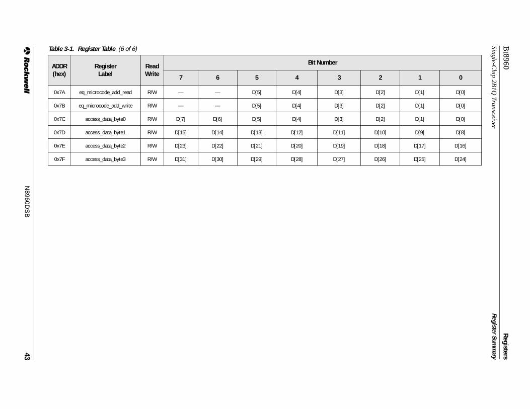
Registers
Register Summ
ary
Bt8960
Single-Chip 2B
1Q Transceiver
43 N
8960DS
B
D[2] D[1] D[0]
D[2] D[1] D[0]
D[2] D[1] D[0]
D[10] D[9] D[8]
D[18] D[17] D[16]
D[26] D[25] D[24]
2 1 0
0x7A eq_microcode_add_read R/W — — D[5] D[4] D[3]
0x7B eq_microcode_add_write R/W — — D[5] D[4] D[3]
0x7C access_data_byte0 R/W D[7] D[6] D[5] D[4] D[3]
0x7D access_data_byte1 R/W D[15] D[14] D[13] D[12] D[11]
0x7E access_data_byte2 R/W D[23] D[22] D[21] D[20] D[19]
0x7F access_data_byte3 R/W D[31] D[30] D[29] D[28] D[27]
Table 3-1. Register Table (6 of 6)
ADDR(hex)
RegisterLabel
ReadWrite
Bit Number
7 6 5 4 3
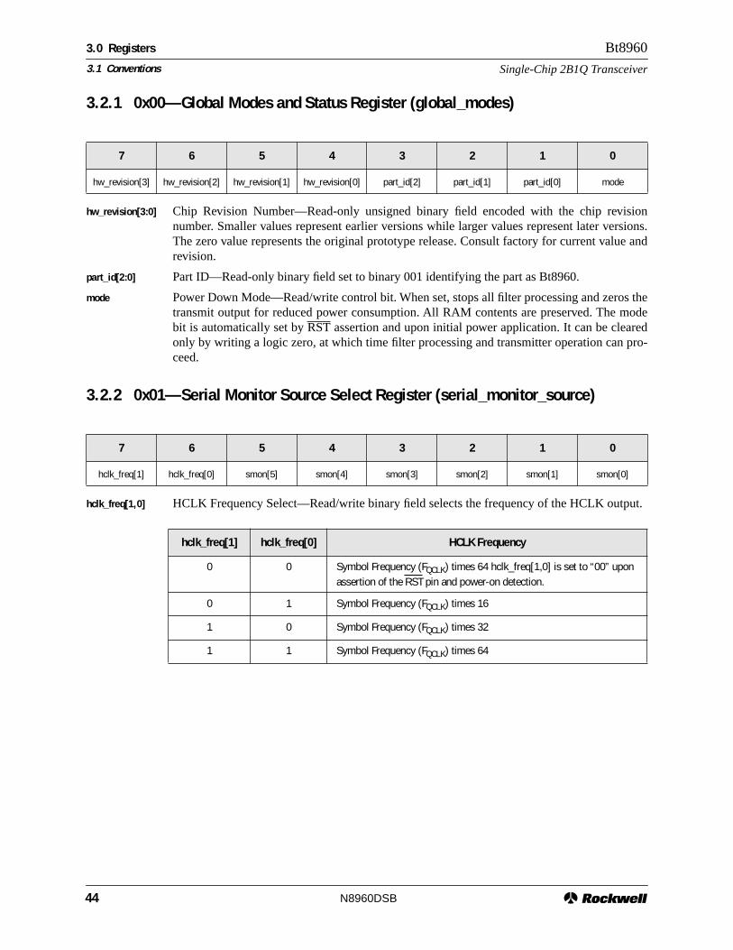
3.0 Registers 3.1 Conventions
Bt8960
Single-Chip 2B1Q Transceiver
3.2.1 0x00—Global Modes and Status Register (global_modes)
hw_revision[3:0] Chip Revision Number—Read-only unsigned binary field encoded with the chip revisionnumber. Smaller values represent earlier versions while larger values represent later versions.The zero value represents the original prototype release. Consult factory for current value andrevision.
part_id[2:0] Part ID—Read-only binary field set to binary 001 identifying the part as Bt8960.
mode Power Down Mode—Read/write control bit. When set, stops all filter processing and zeros thetransmit output for reduced power consumption. All RAM contents are preserved. The modebit is automatically set by RST assertion and upon initial power application. It can be clearedonly by writing a logic zero, at which time filter processing and transmitter operation can pro-ceed.
3.2.2 0x01—Serial Monitor Source Select Register (serial_monitor_source)
hclk_freq[1,0] HCLK Frequency Select—Read/write binary field selects the frequency of the HCLK output.
7 6 5 4 3 2 1 0
hw_revision[3] hw_revision[2] hw_revision[1] hw_revision[0] part_id[2] part_id[1] part_id[0] mode
7 6 5 4 3 2 1 0
hclk_freq[1] hclk_freq[0] smon[5] smon[4] smon[3] smon[2] smon[1] smon[0]
hclk_freq[1] hclk_freq[0] HCLK Frequency
0 0 Symbol Frequency (FQCLK) times 64 hclk_freq[1,0] is set to “00” upon assertion of the RST pin and power-on detection.
0 1 Symbol Frequency (FQCLK) times 16
1 0 Symbol Frequency (FQCLK) times 32
1 1 Symbol Frequency (FQCLK) times 64
44 N8960DSB

3.0 Registers
3.1 Conventions
Bt8960
Single-Chip 2B1Q Transceiver
smon[5:0] Serial Monitor Source Select—Read/write binary field selects the Serial Monitor (SMON) out-put source.
3.2.3 0x02—Interrupt Mask Register Low (mask_low_reg)
Independent read/write mask bits for each of the Timer Source Register [timer_source; 0x04] interrupt flags. Alogic one represents the masked condition. A logic zero represents the unmasked condition. All mask bitsbehave identically with respect to their corresponding interrupt flags. Setting a mask bit prevents the corre-sponding interrupt flag from affecting the IRQ output. Clearing a mask allows the interrupt flag to affect IRQoutput. Unmasking an active interrupt flag will immediately cause the IRQ output to go active, if currently inac-tive. Masking an active interrupt flag will cause IRQ to go inactive, if no other unmasked interrupt flags are set.
t4 General Purpose Timer 4
t3 General Purpose Timer 3
snr SNR Alarm Timer
meter Meter Timer
sut4 Startup Timer 4
sut3 Startup Timer 3
sut2 Startup Timer 2
sut1 Startup Timer 1
smon[5:0]Source
Decimal Binary
0 – 47 00 0000 – 10 1111 Equalizer Register File
48 11 0000 Digital Front-End Output/LEC Input
49 11 0001 Linear Echo Replica
50 11 0010 DFE Subtactor Output/EP Input
51 11 0011 EP Subtractor Output/Slicer Input
52 11 0100 Timing Recovery Phase Detector Output/Loop Filter Input
53 11 0101 Timing Recovery Loop Filter Output/Frequency Synthesizer Input
7 6 5 4 3 2 1 0
t4 t3 snr meter su4 sut3 sut2 sut1
45 N8960DSB

3.0 Registers 3.1 Conventions
Bt8960
Single-Chip 2B1Q Transceiver
3.2.4 0x03—Interrupt Mask Register High (mask_high_reg)
Independent read/write mask bits for each of the IRQ Source Register [irq_source; 0x05] interrupt flags. Indi-vidual mask bit behavior is identical to that specified for Interrupt Mask Register Low [mask_low_reg; 0x02].
sync Sync Indication
high_felm Far-End Level Meter High Alarm
low_felm Far-End Level Meter High Alarm
low_snr Signal-to-Noise Ratio Low Alarm
3.2.5 0x04—Timer Source Register (timer_source)
Independent read/write (zero only) interrupt flags, one for each of eight internal timers. Each flag bit is set andstays set when its corresponding timer value transitions from one to zero. If unmasked, this event will cause theIRQ output to be activated. Flags are cleared by writing them with a logic zero value. Once cleared, a steady-state timer value of zero will not cause a flag to be reasserted. Clearing an unmasked flag will cause the IRQoutput to return to the inactive state, if no other unmasked interrupt flags are set.
t4 General Purpose Timer 4
t3 General Purpose Timer 3
snr SNR Alarm Timer
meter Meter Timer
sut4 Startup Timer 4
sut3 Startup Timer 3
sut2 Startup Timer 2
sut1 Startup Timer 1
7 6 5 4 3 2 1 0
– – – – sync high_felm low_felm low_snr
7 6 5 4 3 2 1 0
t4 t3 snr meter sut4 sut3 sut2 sut1
46 N8960DSB

3.0 Registers
3.1 Conventions
Bt8960
Single-Chip 2B1Q Transceiver
3.2.6 0x05—IRQ Source Register (irq_source)
Independent read/write (zero only) interrupt flags, one for each of four internal sources. Each flag bit is set andstays set when its corresponding source indicates that a valid interrupt condition exists. If unmasked, this eventwill cause the IRQ output to be activated. Writing a logic zero to an interrupt flag whose underlying conditionno longer exists will cause the flag to be immediately cleared. Attempting to clear a flag whose underlying con-dition still exists will not immediately clear the flag, but will allow it to remain set until the underlying conditionexpires, at which time the flag will be cleared automatically. The clearing of an unmasked flag will cause theIRQ output to return to an inactive state, if no other unmasked interrupt flags are set.
sync Sync Indication—Active when the sync detector is enabled and its accumulated equivalentcomparisons exceeds (greater than) the threshold value stored in the Scrambler Sync Thresh-old Register [scr_sync_th; 0x2E].
high_felm Far-End Level Meter High Alarm—Active when the far-end level meter value exceeds (greaterthan) the threshold stored in the Far-End High Alarm Threshold Registers[far_end_high_alarm_th_low, far_end_high_alarm_th_high; 0x30–0x31].
low_felm Far-End Level Meter Low Alarm—Active when the far-end level meter value exceeds (lessthan) the threshold stored in the Far-End Low Alarm Threshold Registers[far_end_low_alarm_th_low, far_end_low_alarm_th_high; 0x32–0x33].
low_snr Signal-to-Noise Ratio Low Alarm—Active when the SNR Alarm meter value exceeds (greaterthan) the threshold stored in the SNR Alarm Threshold Registers [snr_alarm_th_low,snr_alarm_th_high; 0x34–0x35].
3.2.7 0x06—Channel Unit Interface Modes Register (cu_interface_modes)
tbclk_pol Transmit Baud Clock Polarity—Read/write control bit defines the polarity of the TBCLKinput while in the parallel slave interface mode. When set, TQ[1,0] is sampled on the fallingedge of TBCLK; when cleared, TQ[1,0] is sampled on the rising edge.
rbclk_pol Receive Baud Clock Polarity—Read/write control bit defines the polarity of the RBCLK inputwhile in the parallel slave interface mode. When set, RQ[1,0] is updated on the falling edge ofRBCLK; when cleared, RQ[1,0] is updated on the rising edge.
fifos_mode FIFO’s Mode—Read/write control bit used to stagger the transmit and receive FIFO’s read andwrite pointers while in the parallel slave interface mode. A logic one forces the pointers to astaggered position, while a logic zero allows them to operate normally. Must be first set, thencleared once after QCLK-TBCLK-RBCLK frequency lock is achieved to maximize phase-error tolerance.
interface_mode[1,0] Interface Mode—Read/write binary field specifies one of four operating modes for the channel
unit interface.
7 6 5 4 3 2 1 0
– – – – sync high_felm low_felm low_snr
7 6 5 4 3 2 1 0
– – – tbclk_pol rbclk_pol fifos_mode interface_mode[1] interface_mode[0]
47 N8960DSB

3.0 Registers 3.1 Conventions
Bt8960
Single-Chip 2B1Q Transceiver
3.2.8 0x07—Receive Phase Select Register (receive_phase_select)
rphs[3:0] Receive Phase Select—Read/write binary field that defines the relative phase relationshipbetween QCLK and the sampling point of the ADC. The rising edges of QCLK corresponds tothe ADC sampling point when rphs = 0000. Each binary increment of rphs represents a one-sixteenth QCLK period delay in the sampling point relative to QCLK.
3.2.9 0x08—Linear Echo Canceller Modes Register (linear_ec_modes)
enable_dc_tap Enable DC Tap—Read/write control bit which, when set, forces a constant +1 value into thelast data tap of the Linear Echo Canceller (LEC). This condition enables cancellation of anyresidual DC offset present at the input to the LEC. When cleared, the last data tap operates nor-mally, as the oldest transmit data sample.
adapt_coefficents Adapt Coefficients—Read/write control bit which enables coefficient adaptation when set; dis-ables/freezes adaptation when cleared. Coefficient values are preserved when adaptation is dis-abled.
zero_coefficients Zero Coefficients—Read/write control bit that continuously zeros all coefficients when set;allows normal coefficient updates, if enabled, when cleared. This behavior differs slightly fromthe similar function (zero_coefficients) of the FFE and EP filters.
Interface mode [1:0]
ModePin Functions
91 90 88 89 85 86
00 Parallel Master —Parallel quat transfer synchronized to QCLK out.
Not used
Not used
RQ[1] RQ[0] TQ[1] TQ[0]
01 Parallel Slave—Parallel quat transfer synchronized to separate TBCLK and RBCLK inputs.
TBCLK RBCLK RQ[1] RQ[0] TQ[1] TQ[0]
10 Serial, Magnitude First. Serial quat transfer synchronized to BCLK out; magnitude-bit first followed by sign bit.
Not used
Not used
RDAT BCLK TDAT Not used
11 Serial, Sign First. Serial quat transfer synchronized to BCLK out; sign-bit first followed by magnitude bit.
Not used
Not used
RDAT BCLK TDAT Not used
7 6 5 4 3 2 1 0
– – – – rphs[3] rphs[2] rphs[1] rphs[0]
7 6 5 4 3 2 1 0
– – enable_dc_tapadapt_
coefficientszero_coefficients zero_output adapt_gain[1] adapt_gain[0]
48 N8960DSB

3.0 Registers
3.1 Conventions
Bt8960
Single-Chip 2B1Q Transceiver
zero_output Zero Output—Read/write control bit which, when set, zeros the echo replica before subtrac-tion from the input signal. Achieves the affect of disabling or bypassing the echo cancellationfunction. Does not disable coefficient adaptation. When cleared, normal echo Canceller opera-tion is performed.
adapt_gain[1,0] Adaptation Gain—Read/write binary field which specifies the adaptation gain.
3.2.10 0x09—Nonlinear Echo Canceller Modes Register (nonlinear_ec_modes)
negate_symbol Negate Symbol—Read/write control bit which, when set, inverts (2’s complement) the receivesignal path at the output of the nonlinear echo canceller. When cleared, the signal path is unaf-fected. This function is independent of all other NEC mode settings.
symbol_delay[2:0] Symbol Delay—Read/write binary field which specifies the number of symbol delays insertedin the transmit symbol input path.
adapt_coefficients Adapt Coefficients—Same function as LEC Modes Register [linear_ec_modes; 0x08].
zero_coefficients Zero Coefficients—Same function as LEC Modes Register.
zero_output Zero Output—Same function as LEC Modes Register.
adapt_gain Adaptation Gain—Read/write control bit which specifies the adaptation gain. When set, theadaptation gain is eight times higher than when cleared.
adapt_gain[1,0] Normalized Gain
00 1
01 4
10 64
11 512
7 6 5 4 3 2 1 0
negate_symbol symbol_delay[2] symbol_delay[1] symbol_delay[0]adapt_
coefficientszero_coefficients zero_output adapt_gain
49 N8960DSB

3.0 Registers 3.1 Conventions
Bt8960
Single-Chip 2B1Q Transceiver
3.2.11 0x0A—Decision Feedback Equalizer Modes Register (dfe_modes)
adapt_coefficents Adapt Coefficients—Read/write control bit which enables coefficient adaptation when set; dis-ables/freezes adaptation when cleared. Coefficient values are preserved when adaptation is dis-abled.
zero_coefficients Zero Coefficients—Read/write control bit which continuously zeros all coefficients when set;allows normal coefficient updates, if enabled, when cleared.
zero_output Zero Output—Read/write control bit which, when set, zeros the equalizer correction signalbefore subtraction from the input signal. Achieves the affect of disabling or bypassing theequalization function. Does not disable coefficient adaptation. When cleared, normal equalizeroperation is performed.
adapt_gain Adaptation Gain—Read/write control bit which specifies the adaptation gain. When set, theadaptation gain is eight times higher than when cleared.
3.2.12 0x0B—Transmitter Modes Register (transmitter_modes)
isolated_pulse[1,0] Isolated Pulse Level Select—Read/write binary field that selects one of four output pulse lev-els while in the isolated pulse transmitter mode.
transmitter_off Transmitter Off—Read/write control bit that zeros the output of the transmitter when set;allows normal transmitter operation (as defined by data_source[2:0]) when cleared.
htur_lfsr Remote Unit (HTU-R/NTU) Polynomial Select—Read/write control bit selects one of twofeedback polynomials for the transmit scrambler. When set, this bit selects the remote unittransmit polynomial (x–23 + x–18 + 1); when cleared, it selects the local unit (HTU-C/LTU)polynomial (x–23 + x–5 + 1).
data_source[2:0] Data Source—Read/write binary field that selects the data source and mode of the transmitteroutput. The transmitter must be enabled (transmitter_off = 0) for these modes to be active.
7 6 5 4 3 2 1 0
– – – –adapt_
coefficientszero_coefficients zero_output adapt_gain
7 6 5 4 3 2 1 0
– isolated_pulse[1] isolated_pulse[0] transmitter_off htur_lfsr data_source[2] data_source[1] data_source[0]
isolated_pulse[1,0] Output Pulse Level
00 –3
01 –1
10 +3
11 +1
50 N8960DSB

3.0 Registers
3.1 Conventions
Bt8960
Single-Chip 2B1Q Transceiver
data_source[2:0] Transmitter Mode
000 Isolated pulse. Level selected by isolated_pulse[1:0]. The meter timer must be enabled and in the continuous mode. The pulse repetition interval is determined by the meter timer countdown interval.
001 Four-level scrambled detector loopback. Sign and magnitude bits from the receiver detector are scrambled and looped back to the transmitter. Feedback polynomial deter-mined by the htur_lfsr control bit.
010 Four-level unscrambled data. Transmits the four-level (2B1Q) sign and magnitude bits from the channel unit transmit interface without scrambling.
011 Four-level scrambled ones. Transmits a scrambled, constant high logic level as a four-level (2B1Q) signal. Feedback polynomial determined by the htur_lfsr control bit.
100 Reserved.
101 Four-level scrambled data. Scrambles and transmits the four-level (2B1Q) sign and mag-nitude bits from the channel unit transmit interface. Feedback polynomial determined by the htur_lfsr control bit.
110 Two-level unscrambled data. Constantly forces the magnitude bit from the channel unit transmit interface to a logic zero and transmits the resulting two-level signal (as deter-mined by the sign bit) without scrambling. Valid output levels limited to +3, –3.
111 Two-level scrambled ones. Transmits a scrambled, constant high-logic level as a two-level signal. Feedback polynomial determined by the htur_lfsr control bit. Scrambler is run at the symbol rate (half-bit rate) to produce the sign bit of the transmitted signal while the magnitude bit is sourced with a constant logic zero. Valid output levels limited to +3, –3.
51 N8960DSB

3.0 Registers 3.1 Conventions
Bt8960
Single-Chip 2B1Q Transceiver
3.2.13 0x0C—Timer Restart Register (timer_restart)
Independent read/write restart bits, one for each of the eight internal timers. Setting an individual bit causes theassociated timer to be reloaded with the contents of its interval register. For the four symbol-rate timers (meter,snr, t3, t4), reloading will occur within one symbol period. For the four startup timers (sut1–4), reloading willoccur within 1,024 symbol periods. Once reloaded, the restart bit is automatically cleared. If a restart bit is setand then cleared (by writing a logic zero) before the reload actually takes place, no timer reload will occur.Once reloaded, if enabled in the Timer Enable Register [timer_enable; 0x0D], the timer will begin countingdown toward zero; otherwise, it will hold at the interval register value.
t4 General Purpose Timer 4
t3 General Purpose Timer 3
snr SNR Alarm Timer
meter Meter Timer
sut4 Startup Timer 4
sut3 Startup Timer 3
sut2 Startup Timer 2
sut1 Startup Timer 1
3.2.14 0x0D—Timer Enable Register (timer_enable)
Independent read/write enable bits, one for each of the eight internal timers. When any individual bit is set, thecorresponding timer is enabled for counting down from its current value toward zero. For the four symbol-ratetimers (meter, snr, t3, t4), counting will begin within one symbol period. For the four startup timers (sut1-4),counting will begin within 1,024 symbol periods. When an enable bit is cleared, the timer is disabled fromcounting while it holds its current value. If an enable bit is set and then cleared before a count actually takesplace, no timer countdown will occur.
t4 General Purpose Timer 4
t3 General Purpose Timer 3
snr SNR Alarm Timer
meter Meter Timer
sut4 Startup Timer 4
sut3 Startup Timer 3
sut2 Startup Timer 2
sut1 Startup Timer 1
7 6 5 4 3 2 1 0
t4 t3 snr meter sut4 sut3 sut2 sut1
7 6 5 4 3 2 1 0
t4 t3 snr meter sut4 sut3 sut2 sut1
52 N8960DSB
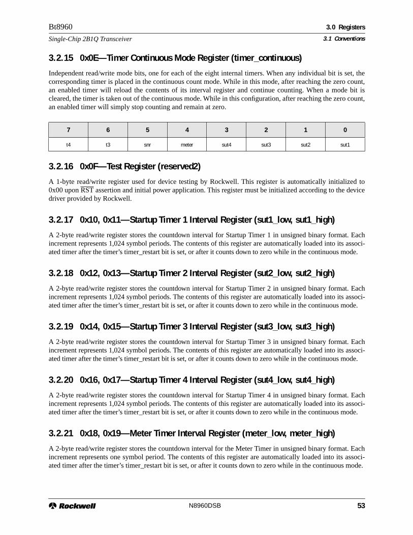
3.0 Registers
3.1 Conventions
Bt8960
Single-Chip 2B1Q Transceiver
3.2.15 0x0E—Timer Continuous Mode Register (timer_continuous)
Independent read/write mode bits, one for each of the eight internal timers. When any individual bit is set, thecorresponding timer is placed in the continuous count mode. While in this mode, after reaching the zero count,an enabled timer will reload the contents of its interval register and continue counting. When a mode bit iscleared, the timer is taken out of the continuous mode. While in this configuration, after reaching the zero count,an enabled timer will simply stop counting and remain at zero.
3.2.16 0x0F—Test Register (reserved2)
A 1-byte read/write register used for device testing by Rockwell. This register is automatically initialized to0x00 upon RST assertion and initial power application. This register must be initialized according to the devicedriver provided by Rockwell.
3.2.17 0x10, 0x11—Startup Timer 1 Interval Register (sut1_low, sut1_high)
A 2-byte read/write register stores the countdown interval for Startup Timer 1 in unsigned binary format. Eachincrement represents 1,024 symbol periods. The contents of this register are automatically loaded into its associ-ated timer after the timer’s timer_restart bit is set, or after it counts down to zero while in the continuous mode.
3.2.18 0x12, 0x13—Startup Timer 2 Interval Register (sut2_low, sut2_high)
A 2-byte read/write register stores the countdown interval for Startup Timer 2 in unsigned binary format. Eachincrement represents 1,024 symbol periods. The contents of this register are automatically loaded into its associ-ated timer after the timer’s timer_restart bit is set, or after it counts down to zero while in the continuous mode.
3.2.19 0x14, 0x15—Startup Timer 3 Interval Register (sut3_low, sut3_high)
A 2-byte read/write register stores the countdown interval for Startup Timer 3 in unsigned binary format. Eachincrement represents 1,024 symbol periods. The contents of this register are automatically loaded into its associ-ated timer after the timer’s timer_restart bit is set, or after it counts down to zero while in the continuous mode.
3.2.20 0x16, 0x17—Startup Timer 4 Interval Register (sut4_low, sut4_high)
A 2-byte read/write register stores the countdown interval for Startup Timer 4 in unsigned binary format. Eachincrement represents 1,024 symbol periods. The contents of this register are automatically loaded into its associ-ated timer after the timer’s timer_restart bit is set, or after it counts down to zero while in the continuous mode.
3.2.21 0x18, 0x19—Meter Timer Interval Register (meter_low, meter_high)
A 2-byte read/write register stores the countdown interval for the Meter Timer in unsigned binary format. Eachincrement represents one symbol period. The contents of this register are automatically loaded into its associ-ated timer after the timer’s timer_restart bit is set, or after it counts down to zero while in the continuous mode.
7 6 5 4 3 2 1 0
t4 t3 snr meter sut4 sut3 sut2 sut1
53 N8960DSB

3.0 Registers 3.1 Conventions
Bt8960
Single-Chip 2B1Q Transceiver
3.2.22 0x20—Test Register (reserved9)
A 1-byte read/write register used for device testing by Rockwell. This register is automatically initialized to0x00 upon RST assertion and initial power application. This register must be initialized according to the devicedriver provided by Rockwell.
3.2.23 0x1A, 0x1B—SNR Alarm Timer Interval Register (snr_timer_low, snr_timer_high)
A 2-byte read/write register stores the countdown interval for the SNR Alarm Timer in unsigned binary format.Each increment represents one symbol period. The contents of this register are automatically loaded into itsassociated timer after the timer’s timer_restart bit is set, or after it counts down to zero while in the continuousmode.
3.2.24 0x1C, 0x1D—General Purpose Timer 3 Interval Register (t3_low, t3_high)
A 2-byte read/write register stores the countdown interval for General Purpose Timer 3 in unsigned binary for-mat. Each increment represents one symbol period. The contents of this register are automatically loaded intoits associated timer after the timer’s timer_restart bit is set, or after it counts down to zero while in the continu-ous mode.
3.2.25 0x1E, 0x1F—General Purpose Timer 4 Interval Register (t4_low, t4_high)
A 2-byte read/write register stores the countdown interval for General Purpose Timer 4 in unsigned binary for-mat. Each increment represents one symbol period. The contents of this register are automatically loaded intoits associated timer after the timer’s timer_restart bit is set, or after it counts down to zero while in the continu-ous mode.
54 N8960DSB

3.0 Registers
3.1 Conventions
Bt8960
Single-Chip 2B1Q Transceiver
3.2.26 0x21—ADC Control Register (adc_control)
loop_back[1,0] Loopback Control—Read/write binary field specifying if loopback is enabled, and the type ofloopback that is enabled. During transmitting loopback, the differential receiver inputs (RXP,RXN) are disabled. The loopback path is intended to go from the transmitter outputs (TXP,TXN), through the external hybrid circuit, back into the differential receiver balance inputs(RXBP, RXBN). During silent loop back, the transmitter is turned off, and the output of thepulse-shaping filter in the transmit section is internally connected to the input of the ADC inthe receive section.
gain[2:0] Gain Control—Read/write binary field specifies the gain of the VGA.
7 6 5 4 3 2 1 0
– – loop_back[1] loop_back[0] – gain[2] gain[1] gain[0]
loop_back[1,0] Function
00 Normal Operation (Loop Back Disabled)
01 Hybrid Inputs Disabled (RXBP, RXBN)
10 Transmitting Loopback
11 Silent Loop Back
gain[2:0] VGA Gain
000 0dB
001 3 dB
010 6 dB
011 9 dB
100 12 dB
101 15 dB
110 15 dB
111 15 dB
55 N8960DSB
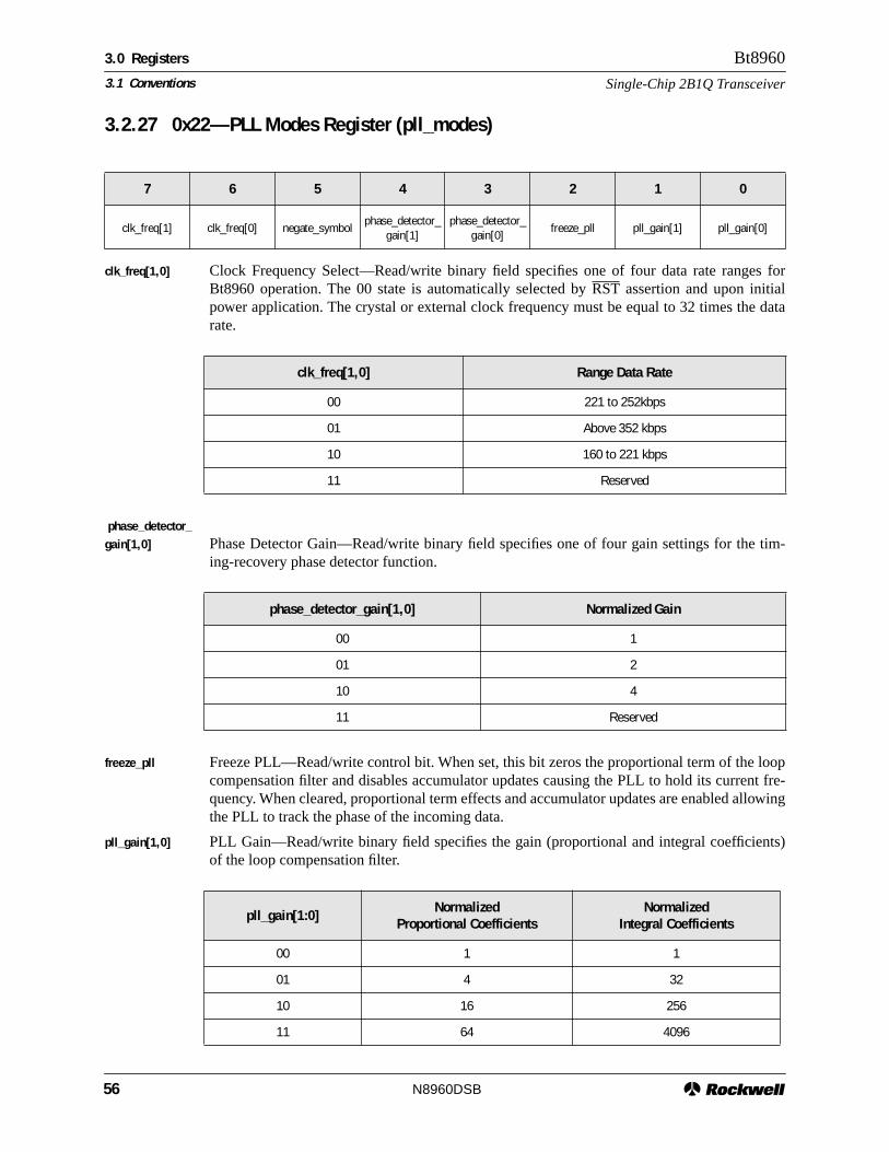
3.0 Registers 3.1 Conventions
Bt8960
Single-Chip 2B1Q Transceiver
3.2.27 0x22—PLL Modes Register (pll_modes)
clk_freq[1,0] Clock Frequency Select—Read/write binary field specifies one of four data rate ranges forBt8960 operation. The 00 state is automatically selected by RST assertion and upon initialpower application. The crystal or external clock frequency must be equal to 32 times the datarate.
phase_detector_gain[1,0] Phase Detector Gain—Read/write binary field specifies one of four gain settings for the tim-
ing-recovery phase detector function.
freeze_pll Freeze PLL—Read/write control bit. When set, this bit zeros the proportional term of the loopcompensation filter and disables accumulator updates causing the PLL to hold its current fre-quency. When cleared, proportional term effects and accumulator updates are enabled allowingthe PLL to track the phase of the incoming data.
pll_gain[1,0] PLL Gain—Read/write binary field specifies the gain (proportional and integral coefficients)of the loop compensation filter.
7 6 5 4 3 2 1 0
clk_freq[1] clk_freq[0] negate_symbolphase_detector_
gain[1]phase_detector_
gain[0]freeze_pll pll_gain[1] pll_gain[0]
clk_freq[1,0] Range Data Rate
00 221 to 252kbps
01 Above 352 kbps
10 160 to 221 kbps
11 Reserved
phase_detector_gain[1,0] Normalized Gain
00 1
01 2
10 4
11 Reserved
pll_gain[1:0] Normalized Proportional Coefficients
NormalizedIntegral Coefficients
00 1 1
01 4 32
10 16 256
11 64 4096
56 N8960DSB

3.0 Registers
3.1 Conventions
Bt8960
Single-Chip 2B1Q Transceiver
3.2.28 0x23—Test Register (reserved10)
A 3-byte read/write register used for device testing by Rockwell. This register is automatically initialized to0x000000 upon RST assertion and initial power application. This register must be initialized according to thedevice driver provided by Rockwell.
3.2.29 0x24, 0x25—Timing Recovery PLL Phase Offset Register (pll_phase_offset_low, pll_phase_offset_high)
A 2-byte read/write register interpreted as a 16-bit, 2’s-complement number. The value of this register is sub-tracted from the output of the timing-recovery phase detector after the phase-detector meter but before the loopcompensation filter.
3.2.30 0x26, 0x27—Receiver DC Offset Register (dc_offset_low, dc_offset_high)
A 2-byte read/write register interpreted as a 16-bit, 2’s-complement number. The value of this register is sub-tracted from the receiver signal path at the output of the digital front end’s format conversion block, ahead of theDC level and signal level meters.
3.2.31 0x28—Transmitter Calibration Register (tx_calibrate)
tx_calibrate[3:0] Transmit Calibrate—4-bit, 2’s-complement, read-only field containing the nominal setting forthe transmitter gain. The value of the Transmit Calibration Register is set during manufactur-ing testing by Rockwell and corresponds to the value required to operate the Bt8960 at a nom-inal 13.5 dBm transmit power, assuming the recommended transformer coupling/hybrid circuitis used. Users may override this calibration by writing their own value into the TransmitterGain Register [tx_gain; 0x29].
7 6 5 4 3 2 1 0
– – tx_calibrate[3] tx_calibrate[2] tx_calibrate[1] tx_calibrate[0] – –
57 N8960DSB

3.0 Registers 3.1 Conventions
Bt8960
Single-Chip 2B1Q Transceiver
3.2.32 0x29—Transmitter Gain Register (tx_gain)
tx_gain[3:0] Transmit Gain—A 4-bit, 2’s-complement, read/write field controlling the transmitter gain.Upon initialization, the value in the Transmitter Calibration Register [tx_calibrate; 0x28] maybe written into this register by software to set the transmitter gain to the nominal value, or theuser may set it to another desired value.
7 6 5 4 3 2 1 0
– – tx_gain[3] tx_gain[2] tx_gain[1] tx_gain[0] – –
tx_gain[3:0] Relative Transmitter Gain (dB)
1000 –1.60
1001 –1.36
1010 –1.13
1011 –0.91
1100 –0.69
1101 –0.48
1110 –0.27
1111 –0.07
0000 0.13
0001 0.32
0010 0.51
0011 0.70
0100 0.88
0101 1.05
0110 1.23
0111 1.40
58 N8960DSB

3.0 Registers
3.1 Conventions
Bt8960
Single-Chip 2B1Q Transceiver
3.2.33 0x2A, 0x2B—Noise-Level Histogram Threshold Register (noise_histogram_th_low, noise_histogram_th_high)
Two-byte read/write register interpreted as a 16-bit, 2’s-complement number. The range of meaningful values islimited to positive integers between 0x0000 and 0x7FFF. The value of this register is compared to the absolutevalue of the slicer error signal produced by the detector. A count of error samples that exceed this threshold(greater than) is accumulated in the noise-level histogram meter.
3.2.34 0x2C, 0x2D—Error Predictor Pause Threshold Register (ep_pause_th_low, ep_pause_th_high)
Two-byte read/write register interpreted as a 16-bit, 2’s-complement number. The range of meaningful values islimited to positive integers between 0x0000 and 0x7FFF. The value of this register is compared to the absolutevalue of the slicer error signal produced by the detector. The result of this comparison (slicer error greater thanthis threshold) is used to initiate a pause condition by zeroing the output of the error predictor correction signalbefore subtraction from the receive signal path. Error predictor coefficient updates are not affected. The pausecondition lasts for a fixed 5-symbol period from the time the threshold was last exceeded.
3.2.35 0x2E—Scrambler Synchronization Threshold Register (scr_sync_th)
A 7-bit read/write register representing an unsigned binary number. The contents of this register are used to testfor scrambler synchronization during the automatic-scrambler synchronization mode of the symbol detector.The test passes when the count of equivalent scrambler and detector output bits exceeds (greater than) the valueof this register. When the auto-scrambler sync mode is not enabled, the contents of this register are not used.
3.2.36 0x30, 0x31—Far-End High Alarm Threshold Register (far_end_high_alarm_th_low, far_end_high_alarm_th_high)
A 2-byte read/write register interpreted as a 16-bit, 2’s-complement number. The range of meaningful values islimited to positive integers between 0x0000 and 0x7FFF. The value of this register is compared to the value ofthe far-end level meter. If the meter reading exceeds (greater than) this threshold, the high_felm interrupt flag isset in the IRQ Source Register [irq_source; 0x05].
3.2.37 0x32, 0x33—Far-End Low Alarm Threshold Register (far_end_low_alarm_th_low, far_end_low_alarm_th_high)
A 2-byte read/write register interpreted as a 16-bit, 2’s-complement number. The range of meaningful values islimited to positive integers between 0x0000 and 0x7FFF. The value of this register is compared to the value ofthe far-end level meter. If the meter reading exceeds (less than) this threshold, the low_felm interrupt flag is setin the IRQ Source Register [irq_source; 0x05].
7 6 5 4 3 2 1 0
– D[6] D[5] D[4] D[3] D[2] D[1] D[0]
59 N8960DSB

3.0 Registers 3.1 Conventions
Bt8960
Single-Chip 2B1Q Transceiver
3.2.38 0x34, 0x35—SNR Alarm Threshold Register (snr_alarm_th_low, snr_alarm_th_high)
A 2-byte read/write register interpreted as a 16-bit, 2’s-complement number. The range of meaningful values islimited to positive integers between 0x0000 and 0x7FFF. The value of this register is compared to the value ofthe SNR alarm meter. If the meter reading exceeds (greater than) this threshold, the low_snr interrupt flag is setin the IRQ Source Register [irq_source; 0x05].
3.2.39 0x36, 0x37—Cursor Level Register (cursor_level_low, cursor_level_high)
A 2-byte read/write register interpreted as a 16-bit, 2’s-complement number. The range of meaningful values islimited to positive integers between 0x0000 and 0x2AAA (one-third of the maximum positive value). The valueof this register represents the expected level of a noise-free +1 receive symbol at the output of the DFE. It ismultiplied by 2 to produce the positive and negative slicing levels, in addition to zero, used by the symbol detec-tor in four-level slicing mode. This value is also used to scale the detector output when computing the equalizererror and slicer error signals. The detected symbol (–3, –1, +1, +3) is multiplied by the value of this register toproduce the scaled output.
3.2.40 0x38, 0x39—DAGC Target Register (dagc_target_low, dagc_target_high)
A 2-byte read/write register interpreted as a 16-bit, 2’s-complement number. The range of meaningful values islimited to positive integers between 0x0000 and 0x7FFF. The value of this register is subtracted from the abso-lute value of the receive signal at the output of the DAGC function. The difference is used as the error input tothe DAGC while in the self-adaptation mode. In the DAGC’s equalizer-error adaptation mode, the contents ofthis register are not used.
60 N8960DSB

3.0 Registers
3.1 Conventions
Bt8960
Single-Chip 2B1Q Transceiver
3.2.41 0x3A—Symbol Detector Modes Register (detector_modes)
enable_peak_detector Enable Peak Detector—Read/write control bit that enables the peak detection function when
set; disables the function when cleared. When enabled, the peak detector output overrides theslicer output if the peak detection criteria are met. If the criteria are not met, or if the functionis disabled, the slicer output is used and peak detector output is ignored.
output_mux_control[1,0] Output Multiplexer Control—Read/write binary field that selects the source of the detector
output connected to the channel unit receive interface.
scr_out_to_dfe Scrambler Output to DFE—Read/write control bit that selects the source of the detector outputconnected to the DFE and timing recovery module inputs, and the transmitter’s detector loop-back input. When set, this bit selects the scrambler/descrambler function; when cleared, itselects the slicer/peak detector output.
two_level Two-Level Mode—Read/write control bit that selects two-level mode when set, four-levelmode when cleared. Affects the slicer and the scrambler/descrambler function. In two-levelmode, the slicer uses a single threshold set at zero to recover sign bits only; all magnitudeinformation is lost. Scrambler/descrambler updates are slowed to the symbol rate (half the nor-mal bit rate) to process only sign information as well; all magnitude output bits are sourcedwith a constant logic zero value producing two-level symbols constrained to +3 and –3 values.
In 4-level mode, the slicer uses two thresholds derived from the Cursor Level Register[cursor_level_low, cursor_level_high; 0x36–0x37], as well as the zero threshold, to recoverboth sign and magnitude information. The scrambler/descrambler is updated at the full bit rateto process both sign and magnitude bits as well.
lfsr_lock LFSR Lock—Read/write control bit that enables the auto scrambler synchronization mode(lfsr_lock) in the detector when set; disables this mode when cleared. Affects the behavior ofthe scrambler/descrambler function, overriding the descr_on setting. When enabled, thescrambler/descrambler is forced into the descrambler mode for 23 cycles. It is then switched tothe scrambled-ones mode for 128 cycles. While in this mode, the outputs of the scrambler andthe slicer/peak detector are compared against one another. The number of equivalent bits(equal comparisons) is accumulated and compared to the value of the scrambler synchroniza-tion threshold register [scr_sync_th; 0x2E].
At any time during the 128 cycles, if the count exceeds the threshold (greater than), the syncinterrupt flag is set in the IRQ Source Register [irq_source; 0x05] and the process terminateswith the scrambler/descrambler left in the scrambled-ones mode. (The sync interrupt flag can-
7 6 5 4 3 2 1 0
enable_peak_detector
output_mux_control[1]
output_mux_control[0]
scr_out_to_dfe two_level lfsr_lock htur_lfsr descr_on
output_mux_control[1,0] Detector Output to CU Receive Interface
00 Same as scr_out_to_dfe selection.
01 Transmitter loopback output from CU transmit interface.
10 Scrambler/descrambler output.
11 Reserved.
61 N8960DSB

3.0 Registers 3.1 Conventions
Bt8960
Single-Chip 2B1Q Transceiver
not be cleared while lfsr_lock remains high.) After 128 cycles, if the threshold is not exceeded,the accumulator is cleared, the scrambler/descrambler re-enters the descrambler mode foranother 23 cycles, and the process repeats until either sync is achieved or this mode is dis-abled. Once disabled, the sync interrupt flag can be cleared (if active) and the scram-bler/descrambler returns to the mode specified by descr_on.
htur_lfsr Remote Unit (HTU-R/NTU) Polynomial Select—Read/write control bit that selects one of twofeedback polynomials for the scrambler/descrambler. When set, this bit selects the remote unit(HTU-R/NTU) receive polynomial (x–23 + x–5 + 1); when cleared, is selects the local unit(HTU-C/LTU) polynomial (x–23 + x–18 + 1).
descr_on Descrambler/Scrambler Select—Read/write control bit that configures the scrambler/descram-bler function as a descrambler when set, and as a scrambler when cleared. As a scrambler, thisbit can only generate a scrambled all ones sequence (constant high logic-level input); allincoming data is ignored. In the auto scrambler synchronization mode (lfsr_lock = 1), thisselection is overwritten though the value of the control bit is unaffected.
3.2.42 0x3B—Peak Detector Delay Register (peak_detector_delay)
A 4-bit read/write register interpreted as an unsigned binary number. Specifies a number of additional symboldelays inserted in the peak detector input path of the symbol detector. Must be set to a value that equalizes thetotal path delay in each of the peak detector and slicer input paths according to the following formula: peakdetector delay register value = DAGC delays + FFE delays – fixed peak detector input delays. The DAGC andFFE delays are not fixed, but result from the microprogrammed implementation of these functions. If usedunmodified, they equal 0 and 7, respectively. The fixed peak detector input delay is equal to 3.
3.2.43 0x3C—Digital AGC Modes Register (dagc_modes)
eq_error_adaptation Equalizer Error Adaptation—Read/write control bit that selects between the equalizer error
adaptation mode when set, and the self-adaptation mode when cleared. Equalizer error adapta-tion uses the equalizer error signal produced by the slicer as the DAGC error input signal. Inself adaptation, the value of the DAGC Target Register [dagc_target_low, dagc_target_high;0x38–0x39] is subtracted from the absolute value of the receive signal at the output of theDAGC, and this difference is used as the error input signal.
adapt_coefficient Adapt Coefficients—Read/write control bit that enables coefficient adaptation when set; dis-ables/freezes adaptation when cleared. Coefficient values are preserved when adaptation is dis-abled.
adapt_gain Adaptation Gain—Read/write control bit that specifies the adaptation gain. When set, theadaptation gain is eight times higher than when cleared.
7 6 5 4 3 2 1 0
– – – – D[3] D[2] D[1] D[0]
7 6 5 4 3 2 1 0
– – – – –eq_error_adaptation
adapt_coefficient adapt_gain
62 N8960DSB
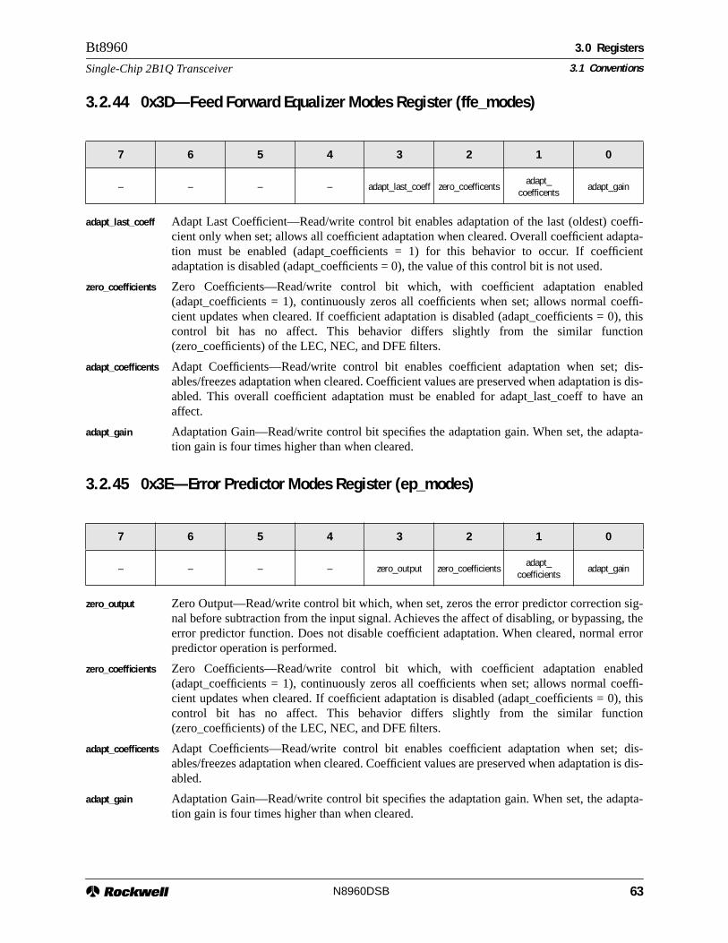
3.0 Registers
3.1 Conventions
Bt8960
Single-Chip 2B1Q Transceiver
3.2.44 0x3D—Feed Forward Equalizer Modes Register (ffe_modes)
adapt_last_coeff Adapt Last Coefficient—Read/write control bit enables adaptation of the last (oldest) coeffi-cient only when set; allows all coefficient adaptation when cleared. Overall coefficient adapta-tion must be enabled (adapt_coefficients = 1) for this behavior to occur. If coefficientadaptation is disabled (adapt_coefficients = 0), the value of this control bit is not used.
zero_coefficients Zero Coefficients—Read/write control bit which, with coefficient adaptation enabled(adapt_coefficients = 1), continuously zeros all coefficients when set; allows normal coeffi-cient updates when cleared. If coefficient adaptation is disabled (adapt_coefficients = 0), thiscontrol bit has no affect. This behavior differs slightly from the similar function(zero_coefficients) of the LEC, NEC, and DFE filters.
adapt_coefficents Adapt Coefficients—Read/write control bit enables coefficient adaptation when set; dis-ables/freezes adaptation when cleared. Coefficient values are preserved when adaptation is dis-abled. This overall coefficient adaptation must be enabled for adapt_last_coeff to have anaffect.
adapt_gain Adaptation Gain—Read/write control bit specifies the adaptation gain. When set, the adapta-tion gain is four times higher than when cleared.
3.2.45 0x3E—Error Predictor Modes Register (ep_modes)
zero_output Zero Output—Read/write control bit which, when set, zeros the error predictor correction sig-nal before subtraction from the input signal. Achieves the affect of disabling, or bypassing, theerror predictor function. Does not disable coefficient adaptation. When cleared, normal errorpredictor operation is performed.
zero_coefficients Zero Coefficients—Read/write control bit which, with coefficient adaptation enabled(adapt_coefficients = 1), continuously zeros all coefficients when set; allows normal coeffi-cient updates when cleared. If coefficient adaptation is disabled (adapt_coefficients = 0), thiscontrol bit has no affect. This behavior differs slightly from the similar function(zero_coefficients) of the LEC, NEC, and DFE filters.
adapt_coefficents Adapt Coefficients—Read/write control bit enables coefficient adaptation when set; dis-ables/freezes adaptation when cleared. Coefficient values are preserved when adaptation is dis-abled.
adapt_gain Adaptation Gain—Read/write control bit specifies the adaptation gain. When set, the adapta-tion gain is four times higher than when cleared.
7 6 5 4 3 2 1 0
– – – – adapt_last_coeff zero_coefficentsadapt_
coefficentsadapt_gain
7 6 5 4 3 2 1 0
– – – – zero_output zero_coefficientsadapt_
coefficientsadapt_gain
63 N8960DSB

3.0 Registers 3.1 Conventions
Bt8960
Single-Chip 2B1Q Transceiver
3.2.46 0x40, 0x41—Phase Detector Meter Register (pdm_low, pdm_high)
A 2-byte read-only register containing the 16 MSBs of the 26-bit, 2’s-complement phase detector meter accu-mulator. This meter sums the output of the timing recovery module’s phase detector—prior to being offset bythe Phase Offset Register [pll_phase_offset_low, pll_phase_offset_high; 0x24, 0x25]—over each Meter Timercountdown interval. Automatically loaded at the end of each interval, the meter register must be read low bytefirst, followed by high byte, unseparated by any other meter-register read access.
3.2.47 0x42—Overflow Meter Register (overflow_meter)
A single-byte read-only register containing all 8 bits of the unsigned overflow meter accumulator. This metercounts the number of ADC overflow conditions which occur during each Meter Timer countdown interval, lim-ited to a maximum count of 255 (0xFF). The meter register is automatically loaded at the end of each count-down interval.
3.2.48 0x44, 0x45—DC Level Meter Register (dc_meter_low, dc_meter_high)
A 2-byte read-only register containing the 16 MSBs of the 32-bit, 2’s-complement DC-level meter accumulator.This meter sums the value of the receive signal input path—after format conversion and DC offset correctionbut before echo cancellation—over each Meter Timer countdown interval. Automatically loaded at the end ofeach interval, the meter register must be read low byte first, followed by high byte, unseparated by any othermeter-register read access.
7 6 5 4 3 2 1 0
D[17] D[16] D[15] D[14] D[13] D[12] D[11] D[10]
D[25] D[24] D[23] D[22] D[21] D[20] D[19] D[18]
7 6 5 4 3 2 1 0
D[7] D[6] D[5] D[4] D[3] D[2] D[1] D[0]
7 6 5 4 3 2 1 0
D[23] D[22] D[21] D[20] D[19] D[18] D[17] D[16]
D[31] D[30] D[29] D[28] D[27] D[26] D[25] D[24]
64 N8960DSB
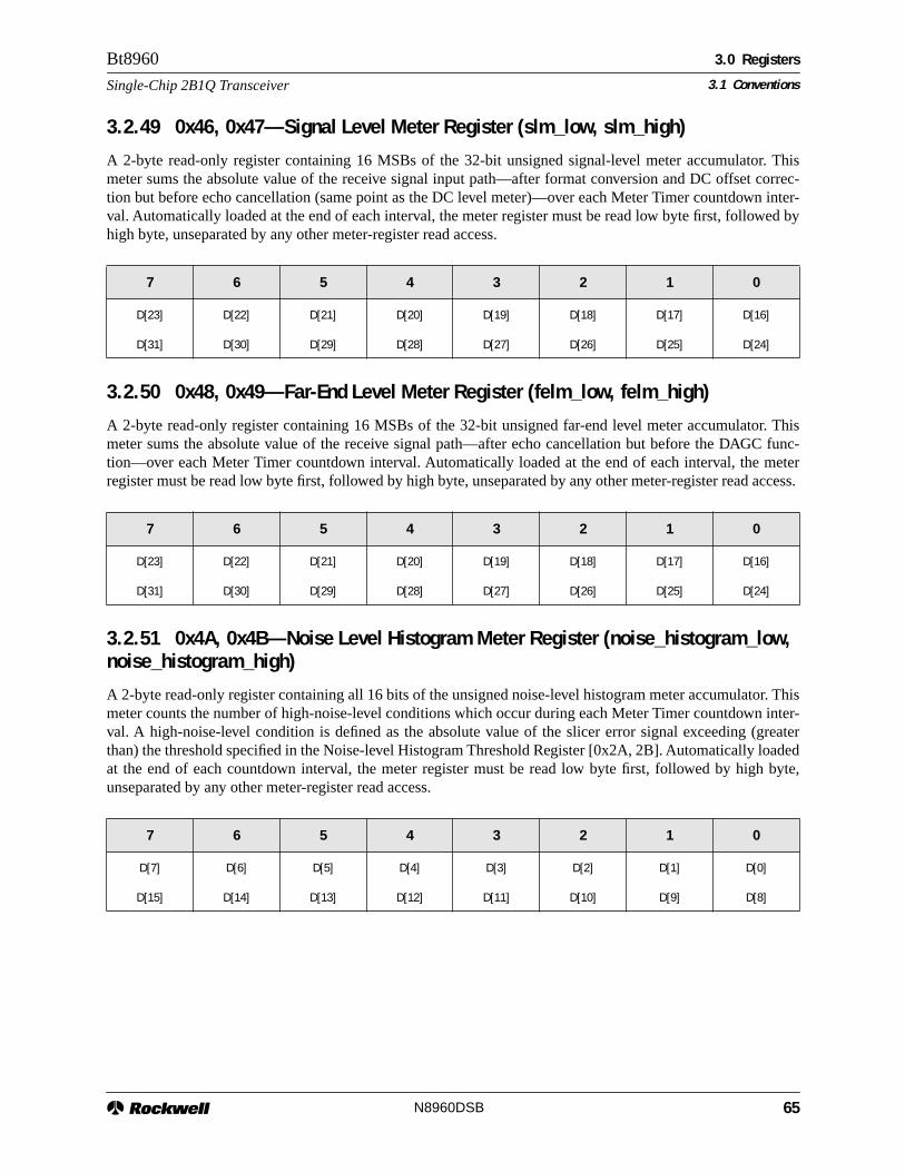
3.0 Registers
3.1 Conventions
Bt8960
Single-Chip 2B1Q Transceiver
3.2.49 0x46, 0x47—Signal Level Meter Register (slm_low, slm_high)
A 2-byte read-only register containing 16 MSBs of the 32-bit unsigned signal-level meter accumulator. Thismeter sums the absolute value of the receive signal input path—after format conversion and DC offset correc-tion but before echo cancellation (same point as the DC level meter)—over each Meter Timer countdown inter-val. Automatically loaded at the end of each interval, the meter register must be read low byte first, followed byhigh byte, unseparated by any other meter-register read access.
3.2.50 0x48, 0x49—Far-End Level Meter Register (felm_low, felm_high)
A 2-byte read-only register containing 16 MSBs of the 32-bit unsigned far-end level meter accumulator. Thismeter sums the absolute value of the receive signal path—after echo cancellation but before the DAGC func-tion—over each Meter Timer countdown interval. Automatically loaded at the end of each interval, the meterregister must be read low byte first, followed by high byte, unseparated by any other meter-register read access.
3.2.51 0x4A, 0x4B—Noise Level Histogram Meter Register (noise_histogram_low, noise_histogram_high)
A 2-byte read-only register containing all 16 bits of the unsigned noise-level histogram meter accumulator. Thismeter counts the number of high-noise-level conditions which occur during each Meter Timer countdown inter-val. A high-noise-level condition is defined as the absolute value of the slicer error signal exceeding (greaterthan) the threshold specified in the Noise-level Histogram Threshold Register [0x2A, 2B]. Automatically loadedat the end of each countdown interval, the meter register must be read low byte first, followed by high byte,unseparated by any other meter-register read access.
7 6 5 4 3 2 1 0
D[23] D[22] D[21] D[20] D[19] D[18] D[17] D[16]
D[31] D[30] D[29] D[28] D[27] D[26] D[25] D[24]
7 6 5 4 3 2 1 0
D[23] D[22] D[21] D[20] D[19] D[18] D[17] D[16]
D[31] D[30] D[29] D[28] D[27] D[26] D[25] D[24]
7 6 5 4 3 2 1 0
D[7] D[6] D[5] D[4] D[3] D[2] D[1] D[0]
D[15] D[14] D[13] D[12] D[11] D[10] D[9] D[8]
65 N8960DSB

3.0 Registers 3.1 Conventions
Bt8960
Single-Chip 2B1Q Transceiver
3.2.52 0x4C, 0x4D—Bit Error Rate Meter Register (ber_meter_low, ber_meter_high)
A 2-byte read-only register containing all 16 bits of the unsigned bit-error-rate meter accumulator. This metercounts the number of error-free bits recovered by the detector during each Meter Timer countdown interval. Anerror-free bit is defined as a match (equal comparison) of the detector’s slicer/peak detector output and itsscrambler/descrambler output, when operating as a scrambler. When operating as a descrambler, the meter sim-ply counts the number of logic ones produced by the descrambler. The meter register is automatically loaded atthe end of each countdown interval, and must be read low byte first, followed by high byte, unseparated by anyother meter-register read access.
3.2.53 0x4E—Symbol Histogram Meter Register (symbol_histogram)
A single-byte read-only register containing 8 MSBs of the 16-bit unsigned symbol histogram meter accumula-tor. This meter counts the number of plus-one or minus-one symbols (+1, –1) detected during each Meter Timercountdown interval. No increment occurs when a plus-three or minus-three symbol (+3, –3) is detected. Themeter register is automatically loaded at the end of each countdown interval.
3.2.54 0x50, 0x51—Noise Level Meter Register (nlm_low, nlm_high)
A 2-byte read-only register containing 16 MSBs of the 32-bit unsigned noise-level meter accumulator. Thismeter sums the absolute value of the detector’s slicer-error signal over each Meter Timer countdown interval.Automatically loaded at the end of each interval, the meter register must be read the low byte first, followed byhigh byte, unseparated by any other meter-register read access.
7 6 5 4 3 2 1 0
D[7] D[6] D[5] D[4] D[3] D[2] D[1] D[0]
D[15] D[14] D[13] D[12] D[11] D[10] D[9] D[8]
7 6 5 4 3 2 1 0
D[7] D[6] D[5] D[4] D[3] D[2] D[1] D[0]
7 6 5 4 3 2 1 0
D[23] D[22] D[21] D[20] D[19] D[18] D[17] D[16]
D[31] D[30] D[29] D[28] D[27] D[26] D[25] D[24]
66 N8960DSB

3.0 Registers
3.1 Conventions
Bt8960
Single-Chip 2B1Q Transceiver
3.2.55 0x5E, 0x5F— PLL Frequency Register (pll_frequency_low, pll_frequency_high)
A 2-byte read/write register comprising the 16 MSBs of the 31-bit, 2’s-complement timing recovery loop com-pensation filter accumulator. Treated much like a meter register, the frequency register must be read low bytefirst, followed by high byte, unseparated by any timing-function or meter-register read access. Writes mustoccur in the same order, with the low byte written first, followed by the high byte. Write accesses may be sepa-rated by any number of other read or write accesses.
3.2.56 0x70—LEC Read Tap Select Register (linear_ec_tap_select_read)
A 6-bit read/write register representing an unsigned binary address defined over a range of 0 to 59 decimals.When written, it causes the selected 32-bit coefficient of the LEC to be subsequently loaded into the AccessData Register [access_data_byte[3:0]; 0x7C–0x7F] within two symbol periods. Does not affect the value of thecoefficient.
3.2.57 0x71—LEC Write Tap Select Register (linear_ec_tap_select_write)
A 6-bit read/write register representing an unsigned binary address defined over a range of 0 to 59 decimals.When written, it causes all 32 bits of the Access Data Register [access_data_byte[3:0]; 0x7C–0x7F] to be sub-sequently written to the selected LEC coefficient within two symbol periods. Does not affect the value of theaccess data register.
3.2.58 0x72—NEC Read Tap Select Register (nonlinear_ec_tap_select_read)
A 6-bit read/write register representing an unsigned binary address defined over a range of 0 to 63 decimals.When written, it causes the selected 14-bit coefficient of the NEC to be subsequently loaded into the lowest-order bits of the Access Data Register [access_data_byte[3:0]; 0x7C–0x7F] within two symbol periods. Doesnot affect the value of the coefficient.
7 6 5 4 3 2 1 0
D[22] D[21] D[20] D[19] D[18] D[17] D[16] D[15]
D[30] D[29] D[28] D[27] D[26] D[25] D[24] D[23]
7 6 5 4 3 2 1 0
– – D[5] D[4] D[3] D[2] D[1] D[0]
7 6 5 4 3 2 1 0
– – D[5] D[4] D[3] D[2] D[1] D[0]
7 6 5 4 3 2 1 0
– – D[5] D[4] D[3] D[2] D[1] D[0]
67 N8960DSB

3.0 Registers 3.1 Conventions
Bt8960
Single-Chip 2B1Q Transceiver
3.2.59 0x73—NEC Write Tap Select Register (nonlinear_ec_tap_select_write)
A 6-bit read/write register representing an unsigned binary address defined over a range of 0 to 63 decimals.When written, it causes the lowest-order 14 bits of the Access Data Register [access_data_byte[3:0]; 0x7C–0x7F] to be subsequently written to the selected NEC coefficient within two symbol periods. Does not affect thevalue of the access data register.
3.2.60 0x74—DFE Read Tap Select Register (dfe_tap_select_read)
A 6-bit read/write register representing an unsigned binary address defined over a range of 0 to 57 decimals.When written, it causes the selected 16-bit coefficient of the DFE to be subsequently loaded into the lowest-order bits of the Access Data Register [access_data_byte[3:0]; 0x7C–0x7F] within two symbol periods. Doesnot affect the value of the coefficient.
3.2.61 0x75—DFE Write Tap Select Register (dfe_tap_select_write)
A 6-bit read/write register representing an unsigned binary address defined over a range of 0 to 57 decimals.When written, it causes the lowest-order 16 bits of the Access Data Register [access_data_byte[3:0]; 0x7C–0x7F] to be subsequently written to the selected DFE coefficient within two symbol periods. Does not affect thevalue of the access data register.
3.2.62 0x76—Scratch Pad Read Tap Select (sp_tap_select_read)
A 6-bit read/write register representing an unsigned binary address defined over a range of 0 to 63 decimals.When written, it causes the selected 8-bit scratch pad memory location to be subsequently loaded into the low-est-order bits of the Access Data Register [access_data_byte[3:0]; 0x7C–0x7F] within two symbol periods.Does not affect the value of the memory.
7 6 5 4 3 2 1 0
– – D[5] D[4] D[3] D[2] D[1] D[0]
7 6 5 4 3 2 1 0
– – D[5] D[4] D[3] D[2] D[1] D[0]
7 6 5 4 3 2 1 0
– – D[5] D[4] D[3] D[2] D[1] D[0]
7 6 5 4 3 2 1 0
– – D[5] D[4] D[3] D[2] D[1] D[0]
68 N8960DSB

3.0 Registers
3.1 Conventions
Bt8960
Single-Chip 2B1Q Transceiver
3.2.63 0x77—Scratch Pad Write Tap Select (sp_tap_select_write)
A 6-bit read/write register representing an unsigned binary address defined over a range of 0 to 63 decimals.When written, it causes the lowest-order 8 bits of the Access Data Register [access_data_byte[3:0]; 0x7C–0x7F] to be subsequently written to the selected scratch pad memory location within two symbol periods. Doesnot affect the value of the access data register.
3.2.64 0x78—Equalizer Read Select Register (eq_add_read)
A 6-bit read/write register representing an unsigned binary address defined over a range of 0 to 47 decimals.When written, it causes the selected 16-bit location of the equalizer register file to be subsequently loaded intothe lowest-order bits of the Access Data Register [access_data_byte[3:0]; 0x7C–0x7F] within two symbol peri-ods. Does not affect the value of the register file location. An address map of the shared register file, as definedby the factory-delivered microcode, is shown below.
7 6 5 4 3 2 1 0
– – D[5] D[4] D[3] D[2] D[1] D[0]
7 6 5 4 3 2 1 0
– – D[5] D[4] D[3] D[2] D[1] D[0]
D[5:0]Stored Parameter
Decimal Binary
0–7 00 0000–00 0111 FFE Coefficients 0–7
8–15 00 1000–00 1111 FFE Data Taps 0–7
16–20 01 0000–01 0100 EP Coefficients 0–4
21–25 01 0101–01 1001 EP Data Taps 0–4
26 01 1010 DAGC Gain - Least-Significant Word
27 01 1011 DAGC Gain - Most-Significant Word
28 01 1100 DAGC Output
29 01 1101 FFE Output
30 01 1110 DAGC Input
31 01 1111 FFE Output, Delayed 1 Symbol Period
32 10 0000 DAGC Error Signal
33 10 0001 Equalizer Error Signal
34 10 0010 Slicer Error Signal
35–47 10 0011–10 1111 Reserved
69 N8960DSB

3.0 Registers 3.1 Conventions
Bt8960
Single-Chip 2B1Q Transceiver
3.2.65 0x79—Equalizer Write Select Register (eq_add_write)
A 6-bit read/write register representing an unsigned binary address defined over a range of 0 to 47 decimals.When written, it causes the lowest-order 16 bits of the Access Data Register [access_data_byte[3:0]; 0x7C–0x7F] to be subsequently written to the selected equalizer register file location within two symbol periods. Doesnot affect the value of the access data register. An address map of the shared register file, as defined by the fac-tory-delivered microcode, is shown below.
3.2.66 0x7A—Equalizer Microcode Read Select Register (eq_microcode_add_read)
A 6-bit read/write register representing an unsigned binary address defined over a range of 0 to 63 decimals.When written, it causes the selected 32-bit location of the equalizer microprogram store to be subsequentlyloaded into the Access Data Register [access_data_byte[3:0]; 0x7C–0x7F] within two symbol periods. Does notaffect the value of the microprogram store location.
3.2.67 0x7B—Equalizer Microcode Write Select Register (eq_microcode_add_write)
A 6-bit read/write register representing an unsigned binary address defined over a range of 0 to 63 decimals.When written, it causes all 32 bits of the Access Data Register [access_data_byte[3:0]; 0x7C–0x7F] to be sub-sequently written to the selected equalizer microprogram store location within two symbol periods. Does notaffect the value of the access data register. Factory-developed equalizer microcode is included with the no-feelicensed HDSL transceiver software available from Rockwell.
3.2.68 0x7C–0x7F—Access Data Register (access_data_byte3:0)
A 4-byte read/write register stores filter coefficient, equalizer register file, and equalizer microprogram storecontents during indirect accesses to these RAM-based locations. Writes to addresses 0x70 through 0x7B, utilizethe contents of this shared register as specified in each of the individual register descriptions.
7 6 5 4 3 2 1 0
– – D[5] D[4] D[3] D[2] D[1] D[0]
7 6 5 4 3 2 1 0
– – D[5] D[4] D[3] D[2] D[1] D[0]
7 6 5 4 3 2 1 0
– – D[5] D[4] D[3] D[2] D[1] D[0]
70 N8960DSB

4.0 Electrical & Mechanical Specifications
4.1 Absolute Maximum Ratings
Stresses above those listed may cause permanent damage to the device. This is a stress rating only. Functionaloperation of the device at these or any other conditions beyond those listed in the operational sections of thisspecification is not implied. Exposure to absolute maximum rating conditions for extended periods may affectdevice reliability.
Table 4-1. Absolute Maximum Ratings
Symbol Parameter Minimum Maximum Units
VSupply Supply Voltage(1) –0.5 +7 V
VI Input Voltage on any Signal Pin(2) –0.5 VDD2 + 0.5 V
TST Storage Temperature –65 +125 ˚C
TVSOL Vapor-Phase Soldering Temperature (1 minute)
+220 ˚C
Notes: (1). VDD1, VDD2, relative to DGND. VAA relative to AGND.(2). Relative to DGND.
71 N8960DSB

4.0 Electrical & Mechanical Specifications 4.2 Recommended Operating Conditions
Bt8960
Single-Chip 2B1Q Transceiver
4.2 Recommended Operating Conditions
Table 4-2. Recommended Operating Conditions
Symbol Parameter Minimum Typical Maximum Units
VDD1 Digital Core-Logic Supply Voltage 4.75 5.0 5.25 V
VDD2 Digital I/O-Buffer Supply Voltage 4.75 5.0 5.25 V
VAA Analog Supply Voltage 4.75 5.0 5.25 V
VIH High-Level Input Voltage 2.0 VDD2 + 0.3 V
VIL Low-Level Input Voltage –0.3 +0.8 V
VIHX High-Level Input Voltage for XTALI / MCLK 0.8*VDD2 VDD2 + 0.3 V
VILX Low-Level Input Voltage for XTALI / MCLK –0.3 0.2*VDD2 V
CL Output Capacitive Loading(1) 60 pF
TA Ambient Operating Temperature(2) –40 +85 ˚C
Notes: (1). Capacitive loading over which all digital output switching characteristics are guaranteed. (2). Still-air temperature range over which all electrical characteristics and timing requirements/characteristics are guaran-
teed.
72 N8960DSB

4.0 Electrical & Mechanical Specifications
4.3 Electrical Characteristics
Bt8960
Single-Chip 2B1Q Transceiver
4.3 Electrical Characteristics
Typical characteristics measured at nominal operating conditions: TA = 25 ˚C; VDD/AA = 5.0 V minimum/maxi-mum characteristics guaranteed over extreme operating conditions: min ≤ TA ≤ max; min ≤ VDD/AA ≤ max.
Table 4-3. Electrical Characteristics
Symbol Parameter Minimum Typical Maximum Units
VOH High-Level Output Voltage @ IOH = –400 µA 2.4 V
VOLL Low-Level Output Voltage @ IOL = 6 mA (IRQ and READY) 0.4 V
VOL Low-Level Output Voltage @ IOL = 3 mA (All Other Outputs) 0.4 V
II Input Leakage Current @ VSS2 ≤ VI ≤ VDD2 ±10 µA
IOZ High-Impedance Output Leakage Current @ VSS2 ≤ VO ≤ VDD2 ±10 µA
IPR Resistive Pull-Up Current @ VI = VSS2 (TDI and TMS) –100 –800 µA
ITOTAL Total Supply Current @ FQCLK = 208 kHz (N=6)(1) 133 147 mA
ITOTAL Total Supply Current @ FQCLK = 144 kHz (N=4)(1) 120 131 mA
ITOTAL Total Supply Current @ FQCLK = 80 kHz (N=2)(1) 106 117 mA
IPD Total Power-Down Current @ FQCLK = 208 kHz (N=6)(2) TBD mA
IPD Total Power-Down Current @ FQCLK = 144 kHz (N=4)(2) TBD mA
IPD Total Power-Down Current @ FQCLK = 80 kHz (N=2)(2) TBD mA
CI Input Capacitance 10 pF
COZ High-Impedance Output Capacitance 10 pF
Notes: (1). ITOTAL = IDD1 + IDD2 + IAA during normal operation. (2). ITOTAL = IDD1 + IDD2 + IAA during power-down operation.
73 N8960DSB
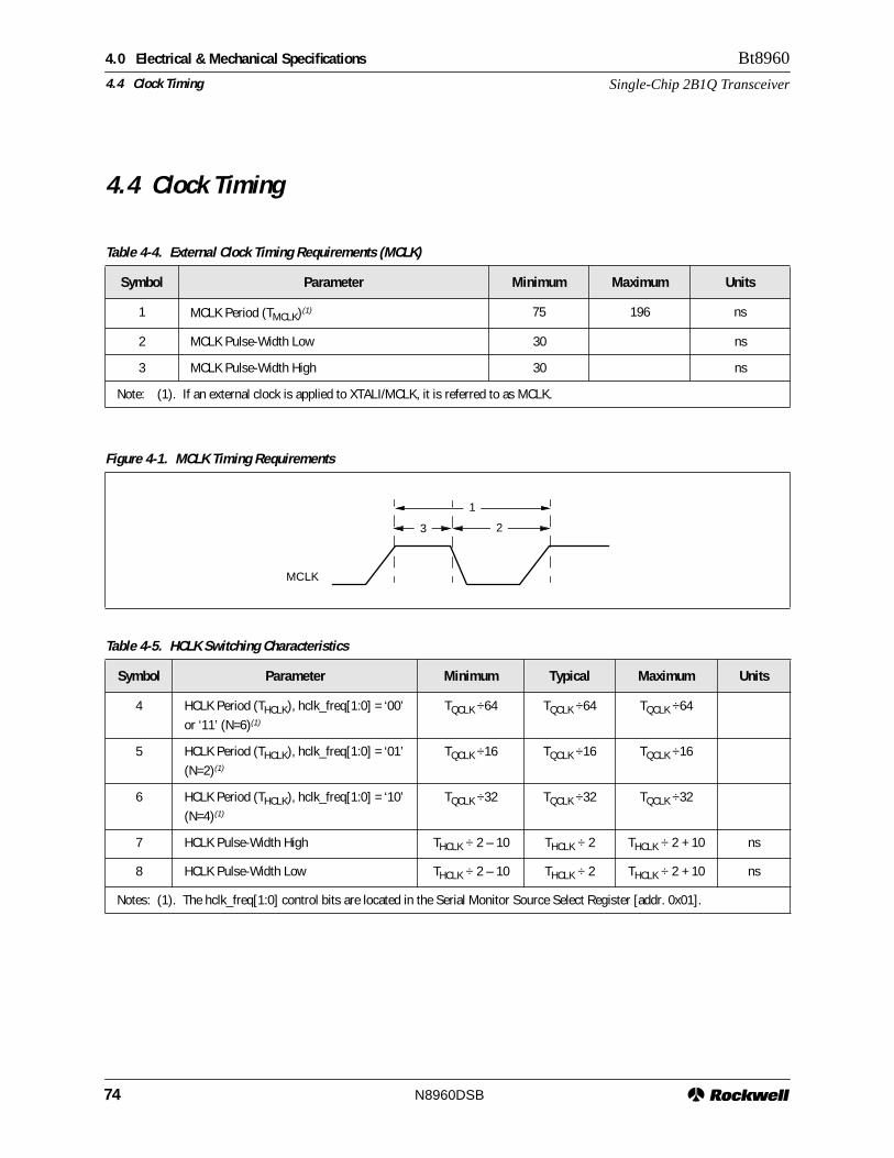
4.0 Electrical & Mechanical Specifications 4.4 Clock Timing
Bt8960
Single-Chip 2B1Q Transceiver
4.4 Clock Timing
Table 4-4. External Clock Timing Requirements (MCLK)
Symbol Parameter Minimum Maximum Units
1 MCLK Period (TMCLK)(1) 75 196 ns
2 MCLK Pulse-Width Low 30 ns
3 MCLK Pulse-Width High 30 ns
Note: (1). If an external clock is applied to XTALI/MCLK, it is referred to as MCLK.
Figure 4-1. MCLK Timing Requirements
3 2
1
MCLK
Table 4-5. HCLK Switching Characteristics
Symbol Parameter Minimum Typical Maximum Units
4 HCLK Period (THCLK), hclk_freq[1:0] = ‘00’ or ‘11’ (N=6)(1)
TQCLK ÷64 TQCLK ÷64 TQCLK ÷64
5 HCLK Period (THCLK), hclk_freq[1:0] = ‘01’ (N=2)(1)
TQCLK ÷16 TQCLK ÷16 TQCLK ÷16
6 HCLK Period (THCLK), hclk_freq[1:0] = ‘10’ (N=4)(1)
TQCLK ÷32 TQCLK ÷32 TQCLK ÷32
7 HCLK Pulse-Width High THCLK ÷ 2 – 10 THCLK ÷ 2 THCLK ÷ 2 + 10 ns
8 HCLK Pulse-Width Low THCLK ÷ 2 – 10 THCLK ÷ 2 THCLK ÷ 2 + 10 ns
Notes: (1). The hclk_freq[1:0] control bits are located in the Serial Monitor Source Select Register [addr. 0x01].
74 N8960DSB
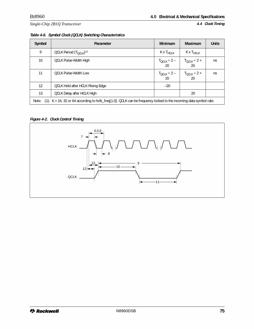
4.0 Electrical & Mechanical Specifications
4.4 Clock Timing
Bt8960
Single-Chip 2B1Q Transceiver
Table 4-6. Symbol Clock (QCLK) Switching Characteristics
Symbol Parameter Minimum Maximum Units
9 QCLK Period (TQCLK)(1) K x THCLK K x THCLK
10 QCLK Pulse-Width High TQCLK ÷ 2 – 20
TQCLK ÷ 2 + 20
ns
11 QCLK Pulse-Width Low TQCLK ÷ 2 – 20
TQCLK ÷ 2 + 20
ns
12 QCLK Hold after HCLK Rising Edge –20
13 QCLK Delay after HCLK High 20
Note: (1). K = 16, 32 or 64 according to hclk_freq[1,0]. QCLK can be frequency locked to the incoming data symbol rate.
Figure 4-2. Clock Control Timing
4,5,6
11
109
7
8
12
13
HCLK
QCLK
75 N8960DSB

4.0 Electrical & Mechanical Specifications 4.5 Channel Unit Interface Timing
Bt8960
Single-Chip 2B1Q Transceiver
4.5 Channel Unit Interface Timing
Table 4-7. Channel Unit Interface Timing Requirements, Parallel Master Mode
Symbol Parameter Minimum Maximum Units
14 TQ[1,0] Setup prior to QCLK Falling Edge 100 ns
15 TQ[1,0] Hold after QCLK Low 25 ns
Table 4-8. Channel Unit Interface Switching Characteristics, Parallel Master Mode
Symbol Parameter Minimum Maximum Units
16 RQ[1,0] Hold after QCLK Rising Edge –50 ns
17 RQ[1,0] Delay after QCLK High 50 ns
Figure 4-3. Channel Unit Interface Timing, Parallel Master Mode
1415
16
17
RQ[1,0]
QCLK
TQ[1,0]
76 N8960DSB

4.0 Electrical & Mechanical Specifications
4.5 Channel Unit Interface Timing
Bt8960
Single-Chip 2B1Q Transceiver
Table 4-9. Channel Unit Interface Timing Requirements, Parallel Slave Mode
Symbol Parameter Minimum Maximum Units
18 TBCLK, RBCLK Period(1) TQCLK TQCLK
19 TBCLK, RBCLK Pulse-Width High TQCLK ÷ 4
20 TBCLK, RBCLK Pulse-Width Low TQCLK ÷ 4
21 TQ[1,0] Setup prior to TBCLK Active Edge(2) 25 ns
22 TQ[1,0] Hold after TBCLK High/Low(2) 25 ns
Notes: (1). TBCLK and RBCLK must be frequency locked to QCLK though they may have independent phase relationships to QCLK and to one another.
(2). TBCLK polarity (edge sensitivity) is programmable through the CU Interface Modes Register [cu_interface_modes 0x06].
Table 4-10. Channel Unit Interface Switching Characteristics, Parallel Slave Mode
Symbol Parameter Minimum Maximum Units
23 RQ[1,0] Hold after RBCLK Active Edge(1) 0 ns
24 RQ[1,0] Delay after RBCLK High/Low(1) 100 ns
Notes: (1). RBCLK polarity (edge sensitivity) is programmable through the CU Interface Modes Register [cu_interface_modes; 0x06].
Figure 4-4. Channel Unit Interface Timing, Parallel Slave Mode
Note: TBCLK and RBCLK polarities are programmable through the CU Interface Modes register. The figure depicts both clocks programmed to falling-edge active.
RQ[1:0]
TBCLK
TQ[1:0]
RBCLK
18
19 20
21 22
23
24
18
19 20
77 N8960DSB
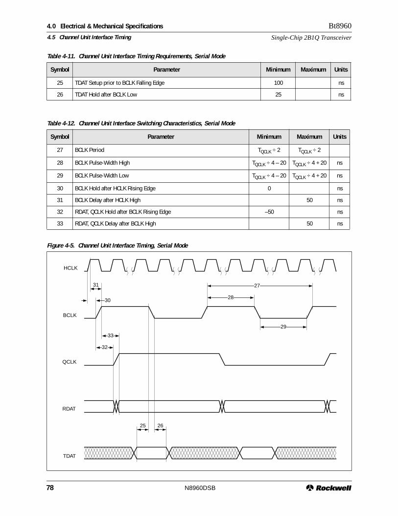
4.0 Electrical & Mechanical Specifications 4.5 Channel Unit Interface Timing
Bt8960
Single-Chip 2B1Q Transceiver
Table 4-11. Channel Unit Interface Timing Requirements, Serial Mode
Symbol Parameter Minimum Maximum Units
25 TDAT Setup prior to BCLK Falling Edge 100 ns
26 TDAT Hold after BCLK Low 25 ns
Table 4-12. Channel Unit Interface Switching Characteristics, Serial Mode
Symbol Parameter Minimum Maximum Units
27 BCLK Period TQCLK ÷ 2 TQCLK ÷ 2
28 BCLK Pulse-Width High TQCLK ÷ 4 – 20 TQCLK ÷ 4 + 20 ns
29 BCLK Pulse-Width Low TQCLK ÷ 4 – 20 TQCLK ÷ 4 + 20 ns
30 BCLK Hold after HCLK Rising Edge 0 ns
31 BCLK Delay after HCLK High 50 ns
32 RDAT, QCLK Hold after BCLK Rising Edge –50 ns
33 RDAT, QCLK Delay after BCLK High 50 ns
Figure 4-5. Channel Unit Interface Timing, Serial Mode
HCLK
BCLK
TDAT
QCLK
RDAT
25 26
27
28
29
30
31
32
33
78 N8960DSB

4.0 Electrical & Mechanical Specifications
4.6 Microcomputer Interface Timing
Bt8960
Single-Chip 2B1Q Transceiver
4.6 Microcomputer Interface Timing
Table 4-13. Microcomputer Interface Timing Requirements
Symbol Parameter Minimum Maximum Units
34 ALE Pulse-Width High 30 ns
35 Address Setup prior to ALE Falling Edge(1) 12 ns
36 Address Hold after ALE Low(1) 5 ns
37 ALE low prior to Write Strobe Falling Edge(2) 20 ns
38 ALE low prior to Read Strobe Falling Edge(3,4) –27 ns
39 Write Strobe Pulse-Width Low(2,5) 2*Tmclk +25 ns
40 Read Strobe Pulse-Width Low(3,5) 2*Tmclk +25 ns
41 Data In Setup prior to Write Strobe Rising Edge(2) 30 ns
42 Data In Hold after Write Strobe High(2) 5 ns
43 R/W Setup prior to Read/Write Strobe Falling Edge 10 ns
44 R/W Hold after Read/Write Strobe High 10 ns
45 ALE Falling Edge after Write Strobe High 20 ns
46 ALE Falling Edge after Read Strobe High 20 ns
47 RST Pulse-Width Low 50 ns
48 Write Strobe Rising Edge after READY low 0 ns
Notes: (1). Address is defined as AD[7:0] when MUXED = 1, and ADDR[7:0] when MUXED = 0.(2). In Intel mode, Write Strobe is defined as WR and CS asserted. In Motorola mode, it is defined as DS and CS asserted
when R/W is low.(3). In Intel mode, Read Strobe is defined as RD and CS asserted. In Motorola mode, it is defined as DS and CS asserted
when R/W is high.(4). Parameter 38 is –27 ns only if separate address and data busses are used (i.e., muxed = 0). If muxed = 1, then parameter
38 is 20 ns.(5). The timing listed is for the synchronous mode of the MCI. It can also be set to synchronous mode by setting bit 0 of the
reserved2 register (address 0x0F) to a 1. In this case the minimum timing changes to 40 us for symbol 39, and 50 us for symbols 40 and 50. Synchronous mode is preferred because it reduces internal switching noise, however no signif-icant performance degradation has been measured as a result of using the asynchronous mode.
79 N8960DSB

4.0 Electrical & Mechanical Specifications 4.6 Microcomputer Interface Timing
Bt8960
Single-Chip 2B1Q Transceiver
Table 4-14. Microcomputer Interface Switching Characteristics
Symbol Parameter Minimum Maximum Units
49 Data Out Enable (Low Z) after Read Strobe Falling Edge(1) 2 ns
50 Data Out Valid after Read Strobe Low(1,7) 2* Tmclk +25 ns
51 Data Out Hold after Read Strobe Rising Edge(1) 2 ns
52 Data Out Disable (High Z) after Read Strobe High(1) 25 ns
53 IRQ Hold after Write Strobe Rising Edge(2,3) 5 ns
54 IRQ Delay after Write Strobe High(2,3) Tqclk ÷ 32 + 20 ns
55 Internal Register Delay after Write Strobe High(3,4) Tqclk ÷ 32 ns
56 Internal RAM Delay after Write Strobe High(3,5) 2*Tqclk ns
57 Access Data Register Delay after Write Strobe High(3,6) 2* Tqclk ns
58 READY Falling Edge after Write Strobe Low(3) 0 2*Tmclk +25 ns
59 READY Rising Edge after Write Strobe High(3) 0 50 ns
60 READY Falling Edge after Read Strobe Low(1) 0 2*Tmclk +25 ns
61 READY Rising Edge after Read Strobe High(1) 0 50 ns
62 Data Out Valid after READY low 10 ns
Notes: (1). Read Strobe is defined as RD and CS asserted in Intel mode, and DS and CS asserted when R/W is high in Motorola mode.
(2). When writing an interrupt mask or status register. (3). Write Strobe is defined as WR and CS asserted in Intel mode, and DS and CS asserted when R/W is low in Motorola
mode. (4). Writes to internal registers are synchronized to an internal 64-times symbol-rate clock. Data is available for reading after
the specified time. This parameter may extend the overall read access time from internal register locations under high bus speed/low symbol rate conditions.
(5). When performing an indirect write to RAM-based locations using a write select register [odd addresses: 0x71–0x7B] and the Access Data Register. Subsequent writes to any read/write select register or the Access Data Register, as initiated by a Write Strobe falling edge, is prohibited for the specified time. This parameter will extend the overall write access time to RAM-based locations under normal bus speed/symbol rate conditions.
(6). When performing an indirect read from RAM-based locations using a read select register [even addresses: 0x70–0x7A] and the Access Data Register. Subsequent writes to any read/write select register, as initiated by a Write Strobe falling edge, is prohibited for the specified time. Data is available for reading from the Access Data Register after the specified time. This parameter will extend the overall read access time from RAM-based locations under normal bus speed/sym-bol rate conditions. Direct writes to the Access Data Register are as specified for internal registers.
(7). The timing listed is for the synchronous mode of the MCI. It can also be set to synchronous mode by setting bit 0 of the reserved2 register (address 0x0F) to a 1. In this case the minimum timing changes to 40 us for symbol 39, and 50 us for symbols 40 and 50. Synchronous mode is preferred because it reduces internal switching noise, however no signif-icant performance degradation has been measured as a result of using the asynchronous mode.
80 N8960DSB
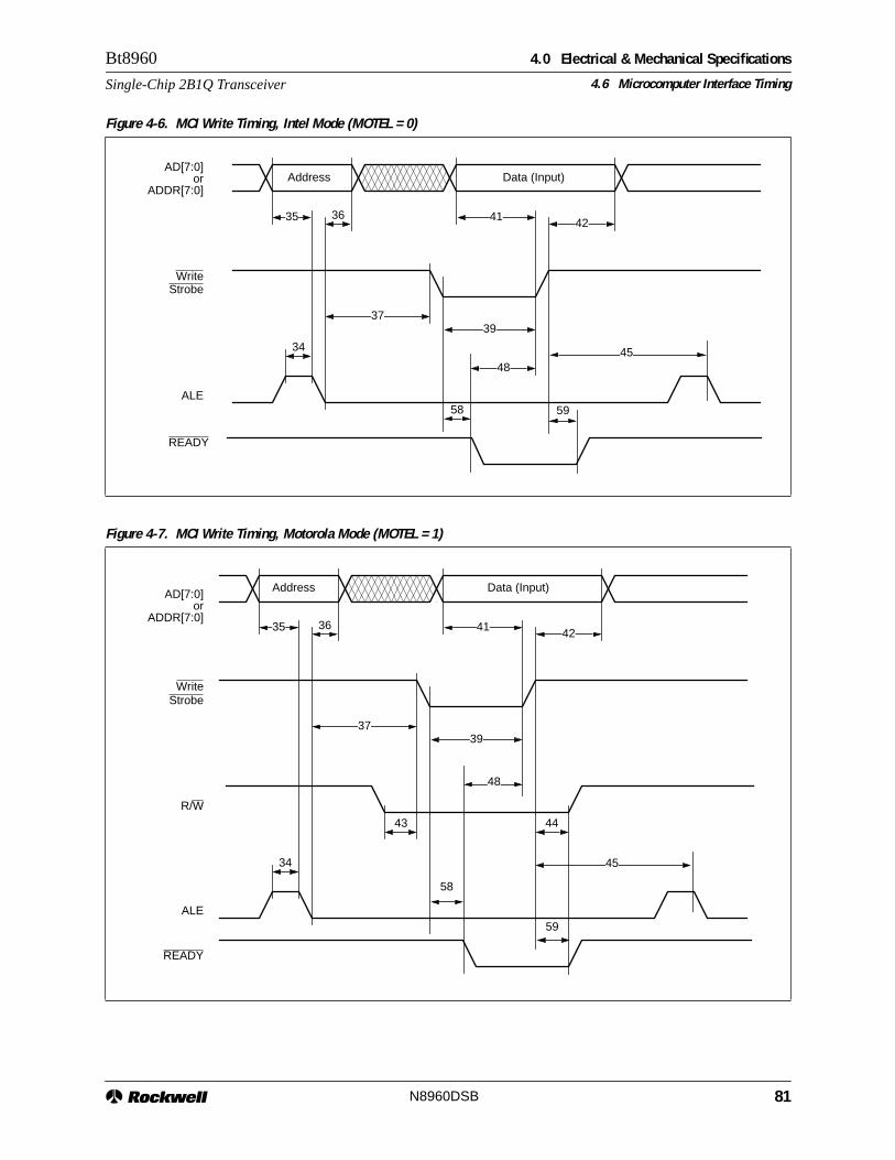
4.0 Electrical & Mechanical Specifications
4.6 Microcomputer Interface Timing
Bt8960
Single-Chip 2B1Q Transceiver
Figure 4-6. MCI Write Timing, Intel Mode (MOTEL = 0)
WriteStrobe
ALE
35 36
37
34
39
41 42
Address Data (Input)
45
AD[7:0]or
ADDR[7:0]
READY
58 59
48
Figure 4-7. MCI Write Timing, Motorola Mode (MOTEL = 1)
AD[7:0]
WriteStrobe
ALE
35 36
37
34
39
41 42
R/W
43 44
Address Data (Input)
45
58
59
orADDR[7:0]
READY
48
81 N8960DSB

4.0 Electrical & Mechanical Specifications 4.6 Microcomputer Interface Timing
Bt8960
Single-Chip 2B1Q Transceiver
Figure 4-8. MCI Read Timing, Intel Mode (MOTEL = 0)
ReadStrobe
ALE
35 36
34
40
51
Address Data (Output)
49
50 52
46
AD[7:0]or
ADDR[7:0]
38
READY
61
60
62
Figure 4-9. MCI Read Timing, Motorola Mode (MOTEL = 1)
ReadStrobe
ALE
35 36
34
40
51
Address Data (Output)
49
50 52
R/W
43 44
46
AD[7:0]or
ADDR[7:0]
38
READY
6160
62
82 N8960DSB

4.0 Electrical & Mechanical Specifications
4.6 Microcomputer Interface Timing
Bt8960
Single-Chip 2B1Q Transceiver
Figure 4-10. Internal Write Timing
IRQ
Write
53
54
Strobe
55
56
InternalRegister
InternalRAM
AccessData
Register
57
83 N8960DSB

4.0 Electrical & Mechanical Specifications 4.6 Microcomputer Interface Timing
Bt8960
Single-Chip 2B1Q Transceiver
4.6.1 Test and Diagnostic Interface Timing
Table 4-15. Test and Diagnostic Interface Timing Requirements
Symbol Parameter Minimum Maximum Units
56 TCK Pulse-Width High 80 ns
57 TCK Pulse-Width Low 80 ns
58 TMS, TDI Setup prior to TCK Rising Edge(1) 20 ns
59 TMS, TDI Hold after TCK High(1) 20 ns
Note: (1). Also applies to functional inputs for SAMPLE/PRELOAD and EXTEST instructions.
Table 4-16. Test and Diagnostic Interface Switching Characteristics
Symbol Parameter Minimum Maximum Units
60 TDO Hold after TCK Falling Edge(1) 0 ns
61 TDO Delay after TCK Low(1) 50 ns
62 TDO Enable (Low Z) after TCK Falling Edge(1) 2 ns
63 TDO Disable (High Z) after TCK Low(1) 25 ns
64 SMON Hold after HCLK Rising Edge(2) 0 ns
65 SMON Delay after HCLK High(2) 50 ns
Notes: (1). Also applies to functional outputs for the EXTEST instruction.(2). HCLK must be programmed to operate at 16 times the symbol rate (16 x FQCLK).
84 N8960DSB

4.0 Electrical & Mechanical Specifications
4.6 Microcomputer Interface Timing
Bt8960
Single-Chip 2B1Q Transceiver
Figure 4-11. JTAG Interface Timing
56
5758 59
60
61
62 63
TDO
TCK
TDITMS
Figure 4-12. SMON Timing
64
65
HCLK
SMON
85 N8960DSB

4.0 Electrical & Mechanical Specifications 4.6 Microcomputer Interface Timing
Bt8960
Single-Chip 2B1Q Transceiver
4.6.2 Analog Specifications
Table 4-17. Receiver Analog Requirements and Specifications
Parameter Comments Min Typ Max Units
Input Signals RXP, RXN, RXBP, and RXBN
Input Voltage Range Balanced Differential –4.5 +4.5 V
Input Resistance DC to 1 MHz 28 kΩ
Common Mode Voltage VCOMI 0.4*VAA
Variable Gain Amplifier (VGA) Six gains from 0 dB to +15 dB
Gain Step 2.55 3.0 3.42 dB
Gain Error ±10 %
Analog-to-Digital Converter
Output Symbol Rate (FQCLK) QCLK frequency (Data Rate/2) 75 210 kHz
Differential Voltage Range (Full Scale Input, FS)(1)
(VRXP–VRXN)—(VRXBP–VRXBN) 5.4 6.0 6.6 VP
Timing Recovery PLL Pull-In Range
±64 ppm
Note: (1). Corresponds to the voltages that will produce a full scale reading from the ADC when the VGA gain equals O dB. Input voltage range is reduced proportionally as VGA gain is increased.
86 N8960DSB
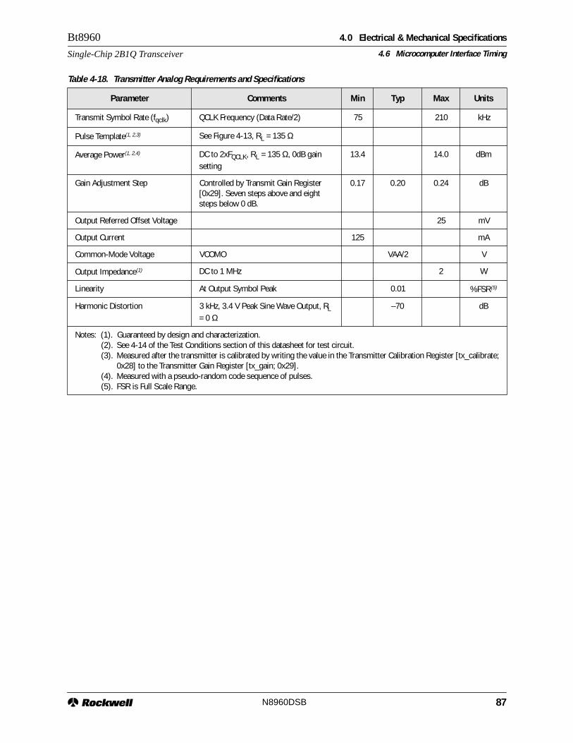
4.0 Electrical & Mechanical Specifications
4.6 Microcomputer Interface Timing
Bt8960
Single-Chip 2B1Q Transceiver
Table 4-18. Transmitter Analog Requirements and Specifications
Parameter Comments Min Typ Max Units
Transmit Symbol Rate (fqclk) QCLK Frequency (Data Rate/2) 75 210 kHz
Pulse Template(1, 2,3) See Figure 4-13, RL = 135 Ω
Average Power(1, 2,4) DC to 2xFQCLK, RL = 135 Ω, 0dB gain setting
13.4 14.0 dBm
Gain Adjustment Step Controlled by Transmit Gain Register [0x29]. Seven steps above and eight steps below 0 dB.
0.17 0.20 0.24 dB
Output Referred Offset Voltage 25 mV
Output Current 125 mA
Common-Mode Voltage VCOMO VAA/2 V
Output Impedance(1) DC to 1 MHz 2 W
Linearity At Output Symbol Peak 0.01 %FSR(5)
Harmonic Distortion 3 kHz, 3.4 V Peak Sine Wave Output, RL = 0 Ω
–70 dB
Notes: (1). Guaranteed by design and characterization.(2). See 4-14 of the Test Conditions section of this datasheet for test circuit.(3). Measured after the transmitter is calibrated by writing the value in the Transmitter Calibration Register [tx_calibrate;
0x28] to the Transmitter Gain Register [tx_gain; 0x29].(4). Measured with a pseudo-random code sequence of pulses.(5). FSR is Full Scale Range.
87 N8960DSB
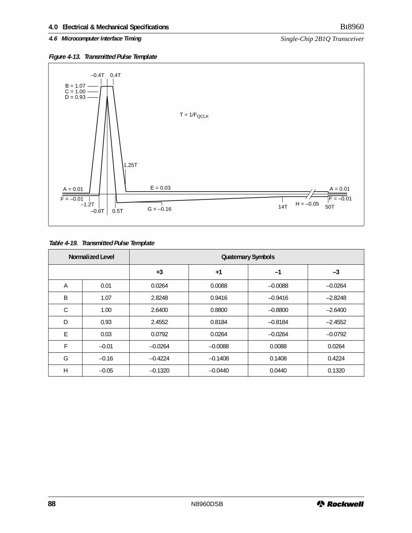
4.0 Electrical & Mechanical Specifications 4.6 Microcomputer Interface Timing
Bt8960
Single-Chip 2B1Q Transceiver
Figure 4-13. Transmitted Pulse Template
B = 1.07C = 1.00D = 0.93
–0.4T 0.4T
1.25T
E = 0.03
G = –0.160.5T–0.6T–1.2T
A = 0.01
F = –0.01
14T
A = 0.01
F = –0.01H = –0.05 50T
T = 1/FQCLK
Table 4-19. Transmitted Pulse Template
Normalized Level Quaternary Symbols
+3 +1 –1 –3
A 0.01 0.0264 0.0088 –0.0088 –0.0264
B 1.07 2.8248 0.9416 –0.9416 –2.8248
C 1.00 2.6400 0.8800 –0.8800 –2.6400
D 0.93 2.4552 0.8184 –0.8184 –2.4552
E 0.03 0.0792 0.0264 –0.0264 –0.0792
F –0.01 –0.0264 –0.0088 0.0088 0.0264
G –0.16 –0.4224 –0.1408 0.1408 0.4224
H –0.05 –0.1320 –0.0440 0.0440 0.1320
88 N8960DSB
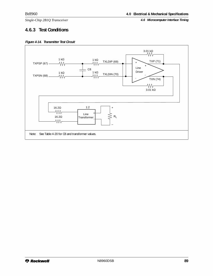
4.0 Electrical & Mechanical Specifications
4.6 Microcomputer Interface Timing
Bt8960
Single-Chip 2B1Q Transceiver
4.6.3 Test Conditions
Figure 4-14. Transmitter Test Circuit
Note: See Table 4-20 for C8 and transformer values.
TXP (71)
TXN (74)
++
--
TXLDIP (69)
TXLDIN (70)
3.01 kΩ
1 kΩ
1 kΩ
3.01 kΩ
1 kΩ
1 kΩ
TXPSP (67)
TXPSN (68)
C8 LineDriver
LineTransformer
+
-RL
1:2 +
_
16.2Ω
16.2Ω
89 N8960DSB
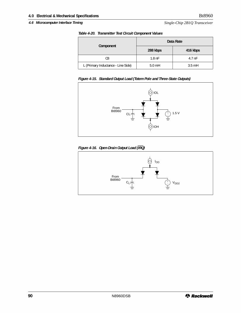
4.0 Electrical & Mechanical Specifications 4.6 Microcomputer Interface Timing
Bt8960
Single-Chip 2B1Q Transceiver
Table 4-20. Transmitter Test Circuit Component Values
ComponentData Rate
288 kbps 416 kbps
C8 1.8 nF 4.7 nF
L (Primary Inductance - Line Side) 5.0 mH 3.5 mH
Figure 4-15. Standard Output Load (Totem Pole and Three-State Outputs)
CL
FromBt8960
IOL
IOH
1.5 V
Figure 4-16. Open-Drain Output Load (IRQ)
FromBt8960
CL
IOD
VDD2
90 N8960DSB

4.0 Electrical & Mechanical Specifications
4.7 Timing Measurements
Bt8960
Single-Chip 2B1Q Transceiver
4.7 Timing Measurements
The input waveforms are shown in Figure 4-17. Output waveforms are displayedin Figures 4-18 and 4-19.
Figure 4-17. Input Waveforms for Timing Tests
3 V
0 V
2.0 V
0.8 V
Input high
Input Low
Input high
Input Low
Figure 4-18. Output Waveforms for Timing Tests
≈VDD
≈0 V
2.4 V
0.4 V
Output high
Output Low
Output high
Output Low
91 N8960DSB

4.0 Electrical & Mechanical Specifications 4.8 Mechanical Specifications
Bt8960
Single-Chip 2B1Q Transceiver
4.8 Mechanical Specifications
Figure 4-19. Output Waveforms for Three-state Enable and Disable Tests
1.7 V
1.3 V
Output Disabled
Output Enabled
1.5 V
VOH - 0.2 V
VOL + 0.2 V
Output Disabled
92 N8960DSB

4.0 Electrical & Mechanical Specifications
4.8 Mechanical Specifications
Bt8960
Single-Chip 2B1Q Transceiver
Figure 4-20. 100-Pin Plastic Quad Flat Pack
93 N8960DSB

e welcome your evaluation of this publication. Your comments and sug-gestions will help us make improve-ments to all current and future
documents. Please rate the following characteristics of the publication you received:
Poor Excellent1. Overall usefulness of the publication.
2. Organization of the publication.
3. Completeness and thoroughness of the material.
4. Clarity and accuracy of the material.
5. Usefulness of the diagrams and illustrations.
6. Quantity of diagrams and Illustrations.
7. Ease of finding specific information.
8. Publication page layout and format.
9. I received the publication(s): (Please mark one).
Within one week after ordering it
Within two weeks after ordering it
Within three or more weeks after ordering it
10. The publication delivery time was: (Please mark one).
Earlier than I needed for my needs
Just in time for my needs
Too late for my needs
11. In what format(s) would you prefer to receive future documents? (Check all that apply.)
Printed books
Internet/PDF delivery
CD-ROM
Other: _____________________________ 12. How would you rank the importance of the fol-
lowing publication features? (1=Very important)____ Publication design and layout____ Accuracy of content____ Detailed diagrams and illustrations____ Receiving the publication in a timely manner
13. We would like to hear your thoughts on how we could improve this publication. Please write your comments or suggestions below:
_____________________________________
_____________________________________
_____________________________________
Thank you for taking the time to evaluate this publi-cation.
Document title:____________________________
Revision No.: _____________________________
Your Name: ______________________________
Title: ____________________________________
Company: ________________________________
E-mail: __________________________________
Phone: __________________________________
W
Please mail or fax this form to:Rockwell Semiconductor Systems
Manager, Technical Publications Dept.(619) 597–4338
READER RESPONSE PAGE