12V Wireless Power Transmitter IC for TX-A6
25
12V Wireless Power Transmitter IC for TX-A6 Product Datasheet P9036B Revision 1.0.0 1 © 2016 Integrated Device Technology, Inc. Features 5W WPC 1.2 Compliant Wireless Power Transmitter Single Chip Solution for TX-A6 Excellent EMI performance eliminates need for EMI filters 12V Operating Input Voltage Closed-Loop Power Transfer Control Between Base Station and Mobile Device Demodulates and Decodes WPC-Compliant Message Packets 5V Regulated DC/DC Converter Integrated RESET Function Internal half-bridge power MOSFETs Proprietary Back-Channel Communication I 2 C Interface Push-Pull GPIO/LED Indicator Outputs Over-Temperature Protection Optional Buzzer Support Foreign Object Detection (FOD) Applications WPC-Compliant Wireless Charging Base Stations Package: 6x6-48 TQFN Description The P9036B is a highly integrated WPC-compliant wireless power transmitter IC for power transmitter WPC design TX-A6. This device operates with a 12Vdc adaptor, and drives an external load directly via an internal half-bridge. It controls the transferred power by changing the switching frequency of the half-bridge inverter from 110 kHz to 205 kHz as specified by the WPC specification for an “A6” transmitter. It contains logic circuits required to demodulate and decode WPC- compliant message packets sent by the mobile device to adjust the transferred power. The P9036B is an intelligent device, which manages mobile device detection, and selection of one of the three coils of the A6 transmitter coil without user supervision. The A6 configuration allows free mobile device positioning over a wider area than configurations that use a single coil, detecting a mobile device for charging while minimizing idle power. Once the mobile device is detected and authenticated, the P9036B continuously monitors all communications from the mobile device, and adjusts the transmitted power accordingly by varying the switching frequency of the internal half-bridge inverter. The P9036B can optionally support a proprietary back-channel communication mode, which enables the device to communicate with IDT’s wireless power receiver solutions. This feature enables additional layers of capabilities beyond the standard WPC requirements. The P9036B includes over-temperature/current protection and WPC compliant Foreign Object Detection (FOD) to protect the base station from overloading in the presence of a metallic foreign object. Additionally, it manages fault conditions associated with power transfer and controls LED outputs to indicate operating status. Mobile Device Receiver Output Load Control System Power Pick-Up Comm Cont Mod Sensing Control Out PWR Base Station Transmitter(s) Input Power Control System Power Generation Comm Cont DeMod IN PWR Sensing Control Induction Load Reflection Comm Control Wireless Interface
Transcript of 12V Wireless Power Transmitter IC for TX-A6

12V Wireless Power Transmitter IC for TX-A6
Product Datasheet P9036B
Revision 1.0.0 1 © 2016 Integrated Device Technology, Inc.
Features 5W WPC 1.2 Compliant Wireless Power
Transmitter Single Chip Solution for TX-A6 Excellent EMI performance eliminates
need for EMI filters 12V Operating Input Voltage Closed-Loop Power Transfer Control Between
Base Station and Mobile Device Demodulates and Decodes WPC-Compliant
Message Packets 5V Regulated DC/DC Converter Integrated RESET Function Internal half-bridge power MOSFETs Proprietary Back-Channel Communication I2C Interface Push-Pull GPIO/LED Indicator Outputs Over-Temperature Protection Optional Buzzer Support Foreign Object Detection (FOD)
Applications WPC-Compliant Wireless Charging Base
Stations
Package: 6x6-48 TQFN
Description The P9036B is a highly integrated WPC-compliant wireless power transmitter IC for power transmitter WPC design TX-A6. This device operates with a 12Vdc adaptor, and drives an external load directly via an internal half-bridge. It controls the transferred power by changing the switching frequency of the half-bridge inverter from 110 kHz to 205 kHz as specified by the WPC specification for an “A6” transmitter. It contains logic circuits required to demodulate and decode WPC-compliant message packets sent by the mobile device to adjust the transferred power.
The P9036B is an intelligent device, which manages mobile device detection, and selection of one of the three coils of the A6 transmitter coil without user supervision. The A6 configuration allows free mobile device positioning over a wider area than configurations that use a single coil, detecting a mobile device for charging while minimizing idle power. Once the mobile device is detected and authenticated, the P9036B continuously monitors all communications from the mobile device, and adjusts the transmitted power accordingly by varying the switching frequency of the internal half-bridge inverter.
The P9036B can optionally support a proprietary back-channel communication mode, which enables the device to communicate with IDT’s wireless power receiver solutions. This feature enables additional layers of capabilities beyond the standard WPC requirements.
The P9036B includes over-temperature/current protection and WPC compliant Foreign Object Detection (FOD) to protect the base station from overloading in the presence of a metallic foreign object. Additionally, it manages fault conditions associated with power transfer and controls LED outputs to indicate operating status.
Mobile DeviceReceiver
Out
put L
oad
Control System
Power Pick-Up
Comm Cont
Mod Sensing Control
OutPWR
Base StationTransmitter(s)
Inpu
t Pow
er
Control System
Power Generation
CommCont
DeMod
INPWR
Sensing Control
Induction
LoadReflection
Comm
Control
WirelessInterface

P9036B
Product Datasheet
Revision 1.0.0 2 © 2016 Integrated Device Technology, Inc.
SIMPLIFIED APPLICATION DIAGRAM
IDTP9036B
REG_
IN
ISNS
HPF
BST
LDO
2P5V
_IN
BUCK
5VT
BUCK
5VT_
IN
GND
LDO5V
LDO2P5V
BUCK
5VT_
SNS
GPIO_0
GPIO_3GPIO_4
EP
VOSNS
GPIO_1GPIO_5
SW
PGND
GPIO_2GPIO_6
LX
+EEPROM
SCLSDAWP BAND
PASS FILTER
Buzzer
LED
A
LED
B
RTH
RESET
EN__ Thermal
Monitoring
PS,VIN
Tx-A6 Coil
PS,GND
RSENSE
CIN
CBSTLBUCK COUT
CS
CISNS,OUT
C5V,OUT
3xFETCOIL,SELECTION
C2P5V,OUT
IN
CBRIDGE,IN
Figure 1. P9036B Simplified Application Schematic
P9036B
Product Datasheet
Revision 1.0.0 3
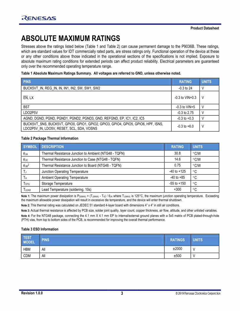
ABSOLUTE MAXIMUM RATINGS Stresses above the ratings listed below (Table 1 and Table 2) can cause permanent damage to the P9036B. These ratings, which are standard values for IDT commercially rated parts, are stress ratings only. Functional operation of the device at these or any other conditions above those indicated in the operational sections of the specifications is not implied. Exposure to absolute maximum rating conditions for extended periods can affect product reliability. Electrical parameters are guaranteed only over the recommended operating temperature range. Table 1 Absolute Maximum Ratings Summary. All voltages are referred to GND, unless otherwise noted.
PINS RATING UNITS BUCK5VT_IN, REG_IN, IN, IN1, IN2, SW, SW1, SW2 -0.3 to 24 V
EN����, LX -0.3 to VIN+0.3 V
BST -0.3 to VIN+5 V LDO2P5V -0.3 to 2.75 V AGND, DGND, PGND, PGND1, PGND2, PGND3, GND, REFGND, EP, IC1, IC2, IC5 -0.3 to +0.3 V BUCK5VT_SNS, BUCK5VT, GPIO0, GPIO1, GPIO2, GPIO3, GPIO4, GPIO5, GPIO6, HPF, ISNS, LDO2P5V_IN, LDO5V, RESET, SCL, SDA, VOSNS -0.3 to +6.0 V
Table 2 Package Thermal Information
SYMBOL DESCRIPTION RATING UNITS θJA Thermal Resistance Junction to Ambient (NTG48 - TQFN) 30.8 °C/W θJC Thermal Resistance Junction to Case (NTG48 - TQFN) 14.6 °C/W θJB2 Thermal Resistance Junction to Board (NTG48 - TQFN) 0.75 °C/W TJ Junction Operating Temperature -40 to +125 °C TA Ambient Operating Temperature -40 to +85 °C TSTG Storage Temperature -55 to +150 °C TLEAD Lead Temperature (soldering, 10s) +300 °C
Note 1: The maximum power dissipation is PD(MAX) = (TJ(MAX) - TA) / θJA where TJ(MAX) is 125°C, the maximum junction operating temperature. Exceeding the maximum allowable power dissipation will result in excessive die temperature, and the device will enter thermal shutdown. Note 2: This thermal rating was calculated on JEDEC 51 standard 4-layer board with dimensions 4” x 4” in still air conditions. Note 3: Actual thermal resistance is affected by PCB size, solder joint quality, layer count, copper thickness, air flow, altitude, and other unlisted variables. Note 4: For the NTG48 package, connecting the 4.1 mm X 4.1 mm EP to internal/external ground planes with a 5x5 matrix of PCB plated-through-hole (PTH) vias, from top to bottom sides of the PCB, is recommended for improving the overall thermal performance.
Table 3 ESD Information
TEST MODEL PINS RATINGS UNITS
HBM All ±2000 V CDM All ±500 V
P9036B Product Datasheet
Revision 1.0.0 4 © 2016 Integrated Device Technology, Inc.
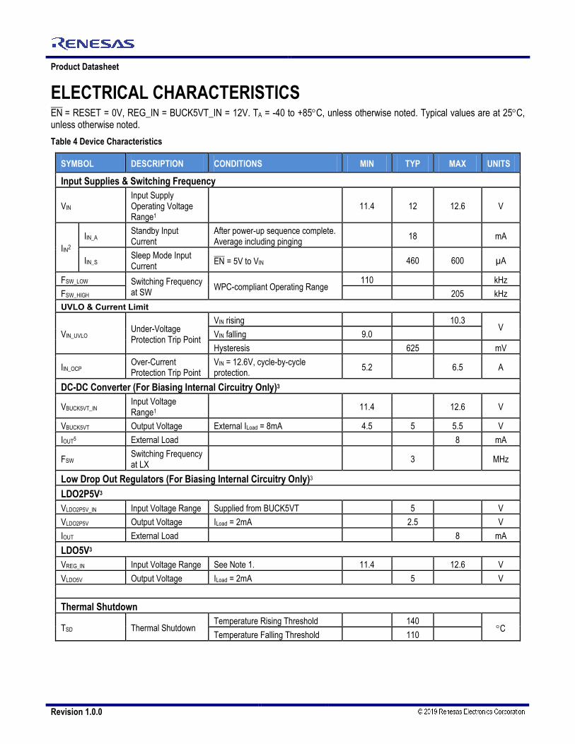
ELECTRICAL CHARACTERISTICS EN���� = RESET = 0V, REG_IN = BUCK5VT_IN = 12V. TA = -40 to +85°C, unless otherwise noted. Typical values are at 25°C, unless otherwise noted. Table 4 Device Characteristics
SYMBOL DESCRIPTION CONDITIONS MIN TYP MAX UNITS
Input Supplies & Switching Frequency
VIN Input Supply Operating Voltage Range1
11.4 12 12.6 V
IIN2 IIN_A Standby Input
Current After power-up sequence complete. Average including pinging 18 mA
IIN_S Sleep Mode Input Current EN���� = 5V to VIN 460 600 µA
FSW_LOW Switching Frequency at SW WPC-compliant Operating Range
110 kHz FSW_HIGH 205 kHz UVLO & Current Limit
VIN_UVLO Under-Voltage Protection Trip Point
VIN rising 10.3 V
VIN falling 9.0 Hysteresis 625 mV
IIN_OCP Over-Current Protection Trip Point
VIN = 12.6V, cycle-by-cycle protection. 5.2 6.5 A
DC-DC Converter (For Biasing Internal Circuitry Only)3
VBUCK5VT_IN Input Voltage Range1 11.4 12.6 V
VBUCK5VT Output Voltage External ILoad = 8mA 4.5 5 5.5 V IOUT5 External Load 8 mA
FSW Switching Frequency at LX 3 MHz
Low Drop Out Regulators (For Biasing Internal Circuitry Only)3 LDO2P5V3
VLDO2P5V_IN Input Voltage Range Supplied from BUCK5VT 5 V VLDO2P5V Output Voltage ILoad = 2mA 2.5 V IOUT External Load 8 mA LDO5V3
VREG_IN Input Voltage Range See Note 1. 11.4 12.6 V VLDO5V Output Voltage ILoad = 2mA 5 V
Thermal Shutdown
TSD Thermal Shutdown Temperature Rising Threshold 140
°C Temperature Falling Threshold 110
P9036B
Product Datasheet
Revision 1.0.0 5
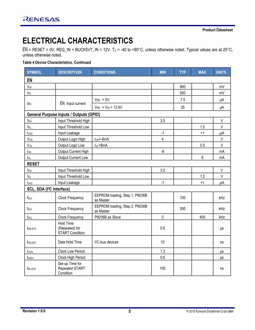
ELECTRICAL CHARACTERISTICS EN���� = RESET = 0V, REG_IN = BUCK5VT_IN = 12V. TA = -40 to +85°C, unless otherwise noted. Typical values are at 25°C, unless otherwise noted. Table 4 Device Characteristics, Continued
SYMBOL DESCRIPTION CONDITIONS MIN TYP MAX UNITS
EN���� VIH 900 mV VIL 550 mV
IEN¯¯ EN¯¯ input current VEN¯¯ = 5V 7.5 μA
VEN¯¯ = VIN = 12.6V 35 μA
General Purpose Inputs / Outputs (GPIO) VIH Input Threshold High 3.5 V VIL Input Threshold Low 1.5 V ILKG Input Leakage -1 +1 µA VOH Output Logic High IOH=-8mA 4 V VOL Output Logic Low IOL=8mA 0.5 V IOH Output Current High -8 mA IOL Output Current Low 8 mA RESET VIH Input Threshold High 3.5 V VIL Input Threshold Low 1.5 V ILKG Input Leakage -1 +1 µA SCL, SDA (I2C Interface)
fSCL Clock Frequency EEPROM loading, Step 1, P9036B as Master 100 kHz
fSCL Clock Frequency EEPROM loading, Step 2, P9036B as Master 300 kHz
fSCL Clock Frequency P9036B as Slave 0 400 kHz
tHD;STA Hold Time (Repeated) for START Condition
0.6 μs
tHD;DAT Data Hold Time I2C-bus devices 10 ns
tLOW Clock Low Period 1.3 μs tHIGH Clock High Period 0.6 μs
tSU;STA Set-up Time for Repeated START Condition
100 ns
P9036B Product Datasheet
Revision 1.0.0 6 © 2016 Integrated Device Technology, Inc.
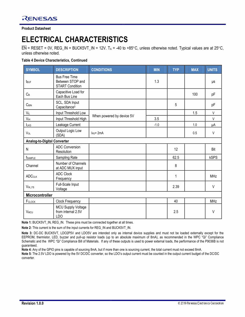
ELECTRICAL CHARACTERISTICS EN���� = RESET = 0V, REG_IN = BUCK5VT_IN = 12V. TA = -40 to +85°C, unless otherwise noted. Typical values are at 25°C, unless otherwise noted. Table 4 Device Characteristics, Continued
SYMBOL DESCRIPTION CONDITIONS MIN TYP MAX UNITS
tBUF Bus Free Time Between STOP and START Condition
1.3 μs
CB Capacitive Load for Each Bus Line 100 pF
CBIN SCL, SDA Input Capacitance5 5 pF
VIL Input Threshold Low When powered by device 5V
1.5 V VIH Input Threshold High 3.5 V ILKG Leakage Current -1.0 1.0 µA
VOL Output Logic Low (SDA) IPD= 2mA 0.5 V
Analog-to-Digital Converter
N ADC Conversion Resolution 12 Bit
fSAMPLE Sampling Rate 62.5 kSPS
Channel Number of Channels at ADC MUX input 8
ADCCLK ADC Clock Frequency 1 MHz
VIN_FS Full-Scale Input Voltage 2.39 V
Microcontroller FCLOCK Clock Frequency 40 MHz
VMCU MCU Supply Voltage from internal 2.5V LDO
2.5 V
Note 1: BUCK5VT_IN, REG_IN. These pins must be connected together at all times. Note 2: This current is the sum of the input currents for REG_IN and BUCK5VT_IN. Note 3: DC-DC BUCK5VT, LDO2P5V and LDO5V are intended only as internal device supplies and must not be loaded externally except for the EEPROM, thermistor, LED, buzzer and pull-up resistor loads (up to an absolute maximum of 8mA), as recommended in the WPC “Qi” Compliance Schematic and the WPC “Qi” Compliance Bill of Materials. If any of these outputs is used to power external loads, the performance of the P9036B is not guaranteed. Note 4: Any of the GPIO pins is capable of sourcing 8mA, but if more than one is sourcing current, the total current must not exceed 8mA. Note 5: The 2.5V LDO is powered by the 5V DC/DC converter, so the LDO’s output current must be counted in the output current budget of the DC/DC converter.
P9036B
Product Datasheet
Revision 1.0.0 7
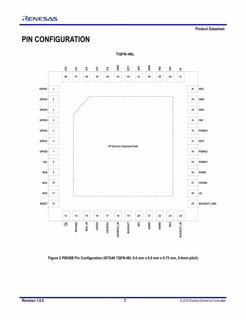
PIN CONFIGURATION
IC6
IC5
IC4
IC3
IC2
GN
D
IC1
HPF
ISN
S
IN2
IN1
IN
36
34
33
32
31
30
29
28
27
26
25
35
NC51GPIO6
TQFN-48L
3
4
5
6
7
8
9
10
11
12
2
13 14 15 16 17 18 19 20 21 22 23 24
48 47 46 45 44 43 42 41 40 39 38 37
GPIO5
GPIO4
GPIO3
GPIO2
GPIO1
GPIO0
SCL
SDA
NC1
NC2
RESET
REFG
ND
REG
_IN
LDO
5V
LDO
2P5V
LDO
2P5V
_IN
BUCK
5VT
BST
AGN
D
DGN
D
NC3
BUCK
5VT_
IN
SW2
SW1
SW
PGND3
NC4
PGND2
PGND1
PGND
VOSNS
LX
BUCK5VT_SNS
EN
EP (Center Exposed Pad)
Figure 2 P9036B Pin Configuration (NTG48 TQFN-48L 6.0 mm x 6.0 mm x 0.75 mm, 0.4mm pitch)

P9036B Product Datasheet
Revision 1.0.0 8 © 2016 Integrated Device Technology, Inc.
PIN DESCRIPTION Table 5 P9036B NTG48 Package Pin Functions by Pin Number
1 GPIO6 I/O General purpose input/output 6.
2 GPIO5 I/O General purpose input/output 5.
3 GPIO4 I/O General purpose input/output 4.
4 GPIO3 I/O General purpose input/output 3.
5 GPIO2 I/O General purpose input/output 2.
6 GPIO1 I/O General purpose input/output 1.
7 GPIO0 I/O General purpose input/output 0.
8 SCL I/O I2C clock.
9 SDA I/O I2C data.
10 NC1 - Internally connected. Must be connected to GND.
11 NC2 - Internally connected. Must be left unconnected.
12 RESET I Active-high chip reset pin. A 47kΩ resistor must be connected between this pin and GND.
13 EN���� I Active-low enable pin. Device is suspended and placed in low current (sleep) mode when pulled high. Tie to GND for stand-alone operation.
14 REFGND - Signal ground connection. Must be connected to AGND.
15 REG_IN1 I LDO5V power supply input. As a minimum, a 1µF ceramic capacitor must be connected between this pin and PGND. This pin must be connected to pin 24.
16 LDO5V2 O 5V LDO output. As a minimum, a 1µF ceramic capacitor must be connected between this pin and PGND.
17 LDO2P5V2 O 2.5V LDO output. As a minimum, a 1µF ceramic capacitor must be connected between this pin and PGND.
18 LDO2P5V_IN I 2.5V LDO input. The LDO2P5V_IN input must be connected to BUCK5VT. As a minimum, a 0.1µF ceramic capacitor must be connected between this pin and GND.
19 BUCK5VT2 I Power and digital supply input to internal circuitry.
P9036B
Product Datasheet
Revision 1.0.0 9
Table 5 P9036B NTG48 Package Pin Functions by Pin Number PIN NAME TYPE DESCRIPTION
20 BST I Bootstrap pin for BUCK converter top switch gate drive supply.
21 AGND - Analog ground connection. Connect to signal ground. Must be connected to REFGND.
22 DGND - Digital ground connection. Must be connected to GND.
23 NC3 - Internally connected. Must be left unconnected.
24 BUCK5VT_IN1 I Buck converter power supply input. As a minimum, a 0.1µF in parallel with a 1µF ceramic capacitor must be connected between this pin and PGND. This pin must be connected to pin 15.
25 BUCK5VT_SNS I Buck regulator feedback. Connect to the high side of the buck converter output capacitor.
26 LX O Switch Node of BUCK converter. Connects to one of the inductor’s terminals.
27 VOSNS I Voltage sense input. This pin can be used to sense voltages such as thermistors, GPIOs, Input voltages. See the Electrical Characteristics Table (VIN_FS) for input voltage limits.
28 PGND - Power ground.
29 PGND1 - Power ground.
30 PGND2 - Power ground.
31 NC4 - Internally connected. Must be left unconnected.
32 PGND3 - Power ground.
33 SW O
Internal – monolithic – power MOSFET, half bridge switching node. These pins drive the transmitter coil. 34 SW1 O
35 SW2 O
36 NC5 - Internally connected. Must be left unconnected.
37 IN I
Internal – monolithic – power MOSFET, half bridge power supply input pins. 38 IN1 I
39 IN2 I
40 ISNS O ISNS output signal. Current used by the transmitter as measured at the input voltage. Attach a 22nF ceramic capacitor to this pin for filtering purposes.
P9036B Product Datasheet
Revision 1.0.0 10 © 2016 Integrated Device Technology, Inc.
Table 5 P9036B NTG48 Package Pin Functions by Pin Number PIN NAME TYPE DESCRIPTION
41 HPF I High pass filter input. This pin is used to read the communication from the receiver.
42 IC1 Reserved for special designs. Must be connected to GND.
43 GND - Ground.
44 IC2 Reserved for special designs. Must be connected to GND.
45 IC3 Reserved for special designs. Must be left unconnected.
46 IC4 Reserved for special designs. Must be left unconnected.
47 IC5 Reserved for special designs. Must be connected to GND.
48 IC6 Reserved for special designs. Must be left unconnected.
49 EP
(Center Exposed Pad)
Thermal
EP, Center Exposed Pad, is on the bottom of the package and must be electrically tied to GND. For good thermal performance, solder to a large copper pad embedded with a pattern of plated through-hole vias. The die is not electrically bonded to the EP, and the EP must not be used as a current-carrying electrical connection.
Note 1: REG_IN, BUCK5VT_IN. These pins must be connected together at all times. Note 2: DC-DC BUCK5VT, LDO2P5V and LDO5V are intended only as internal device supplies and must not be loaded externally except for the EEPROM, thermistor, LED, buzzer and pull-up resistor loads (up to an absolute maximum of 8mA), as recommended in the WPC “Qi” Compliance Schematic and the WPC “Qi” Compliance Bill of Materials.
P9036B
Product Datasheet
Revision 1.0.0 11
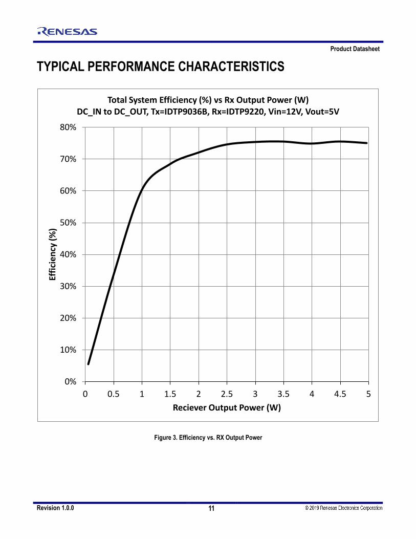
TYPICAL PERFORMANCE CHARACTERISTICS
Figure 3. Efficiency vs. RX Output Power
0%
10%
20%
30%
40%
50%
60%
70%
80%
0 0.5 1 1.5 2 2.5 3 3.5 4 4.5 5
Effic
ienc
y (%
)
Reciever Output Power (W)
Total System Efficiency (%) vs Rx Output Power (W) DC_IN to DC_OUT, Tx=IDTP9036B, Rx=IDTP9220, Vin=12V, Vout=5V

P9036B Product Datasheet
Revision 1.0.0 12 © 2016 Integrated Device Technology, Inc.
BLOCK DIAGRAM
IBIASTHSHDN LDO5V
SW
PGND
VOSNS
IN
SCL
SDA
REG_IN
GND
Micro Controller
Unit(MCU)
GPIO_<6:0>
LDO2P5V
RESET
Demodulator
VIN_UVLO
UVLO_5V/2P5V
VIN_OVP
REFEnable Sequence
LDO2P5V_IN
BUCK5VT_SNS
BUCK5VT_IN
PLLRCOSC
ClockGeneration
I2C
RAM
ROM
OTP
ADC
GPIO
VOSNS
REF
Temp.Signal
Temp.Signal
VINSNSREG_IN
HPF
BUCK5VT
MC
UP
erip
hera
ls
EN����
IDTP9036B
HALF BRIDGEPMOSNMOSFET PAIR
CurrentLimit
ISNS
Dri
ver
Con
trol
LDO5VLDO2P5V
BUCK5VT
3MHZ LX
ISNS
Figure 4. P9036B Internal Functional Block Diagram
P9036B
Product Datasheet
Revision 1.0.0 13
THEORY OF OPERATION The P9036B is a highly-integrated WPC1 (Wireless Power Consortium)-compliant wireless power charging IC solution for the transmitter base station. It can deliver 5W in WPC “Qi” mode using near-field magnetic induction as a means to transfer energy
OVERVIEW
Figure 1 shows the block diagram of the P9036B. When the VIN_UVLO block detects that the voltage at REG_IN and BUCK5VT_IN (connected together externally) is above the Vin_rising UVLO threshold and EN¯¯ is at a logic LOW, the Enable Sequence circuitry activates the voltage reference, the 5V and 2.5V LDOs, and the 5V buck switching regulator.
The voltages at the outputs of the LDOs and the buck regulator are monitored to ensure that they remain in regulation, and the adaptor voltage, coil current, and internal temperature are monitored.
The digital block and the MCU drive an internal half bridge inverter. This inverter powers the transmitter (Tx) coil through the SW pins. The Tx and reciever (Rx) act as a loosely coupled, air core transformer. The Tx coil generates a magnetic field that supplies energy to the Rx coil The Rx uses that field to generate a DC output voltage that is applied to the load.
Communication packets from the receiver in the mobile device are detected and filtered by an external operational amplifier and passive filter, then provided to the HPF pin to be further processed by the Demodulator and converted to digital signals that can be read by the MCU.
Several internal voltages are digitized by the ADC and supplied to the MCU for system control and algorithm –related purposes. Two GPIO ports are available to the system designer for driving LEDs and a buzzer. The clock for the MCU and other circuitry is generated by an internal RC oscillator. I2C SDA and SCL pins permit communication with an external device or host.
Note 1 - Refer to the WPC specification at http://www.wirelesspowerconsortium.com/ for the most current information
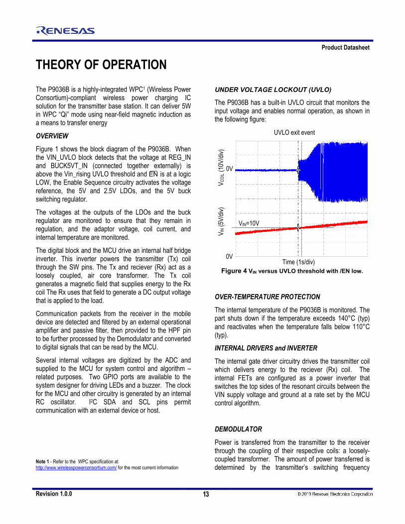
UNDER VOLTAGE LOCKOUT (UVLO)
The P9036B has a built-in UVLO circuit that monitors the input voltage and enables normal operation, as shown in the following figure:
Time (1s/div)
V COI
L (10
V/div
)
UVLO exit event
V IN (
5V/di
v)VIN=10V
0V
0V
Figure 4 VIN versus UVLO threshold with /EN low.
OVER-TEMPERATURE PROTECTION
The internal temperature of the P9036B is monitored. The part shuts down if the temperature exceeds 140°C (typ) and reactivates when the temperature falls below 110°C (typ).
INTERNAL DRIVERS and INVERTER
The internal gate driver circuitry drives the transmitter coil which delivers energy to the reciever (Rx) coil. The internal FETs are configured as a power inverter that switches the top sides of the resonant circuits between the VIN supply voltage and ground at a rate set by the MCU control algorithm.
DEMODULATOR
Power is transferred from the transmitter to the receiver through the coupling of their respective coils: a loosely-coupled transformer. The amount of power transferred is determined by the transmitter’s switching frequency
P9036B Product Datasheet
Revision 1.0.0 14 © 2016 Integrated Device Technology, Inc.
(110kHz-205kHz, by WPC1), and is controlled by the receiver through instructions the receiver sends back through the same coils to the transmitter to increase or decrease power, end power transfer, or another WPC command. The instructions take the form of data packets which the receiver modulates on the carrier. The modulation is detected and then coupled through a series of filters connected to the P9036B’s Demodulator and then fed to the HPF pin. Recovering the data packets is the function of the Demodulator. Decoding and executing the packets is one of the functions of the MCU.
MICROCONTROLLER UNIT (MCU)
The P9036B’s MCU processes the algorithm, commands, and data that control the power transferred to the receiver. The MCU is provided with RAM and ROM, and parametric trim and operational modes are set at the factory through the One-Time Programming (OTP) block, read by the MCU at power-up. Communication with external memory is performed through I2C via the SCL and SDA pins.
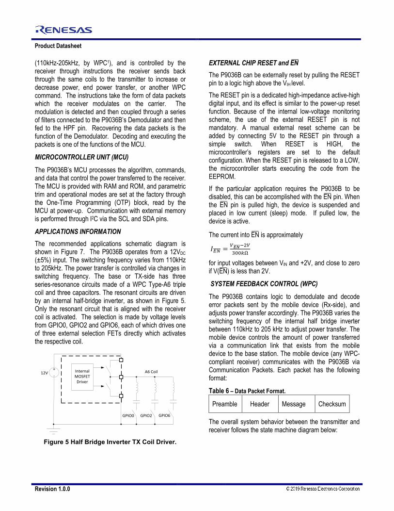
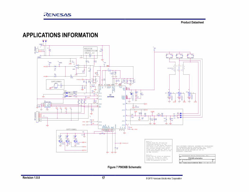
APPLICATIONS INFORMATION The recommended applications schematic diagram is shown in Figure 7. The P9036B operates from a 12VDC (±5%) input. The switching frequency varies from 110kHz to 205kHz. The power transfer is controlled via changes in switching frequency. The base or TX-side has three series-resonance circuits made of a WPC Type-A6 triple coil and three capacitors. The resonant circuits are driven by an internal half-bridge inverter, as shown in Figure 5. Only the resonant circuit that is aligned with the receiver coil is activated. The selection is made by voltage levels from GPIO0, GPIO2 and GPIO6, each of which drives one of three external selection FETs directly which activates the respective coil.
InternalMOSFET
Driver
12V+-
GPIO0 GPIO2 GPIO6
A6 Coil
Figure 5 Half Bridge Inverter TX Coil Driver.
EXTERNAL CHIP RESET and EN¯¯ The P9036B can be externally reset by pulling the RESET pin to a logic high above the VIH level. The RESET pin is a dedicated high-impedance active-high digital input, and its effect is similar to the power-up reset function. Because of the internal low-voltage monitoring scheme, the use of the external RESET pin is not mandatory. A manual external reset scheme can be added by connecting 5V to the RESET pin through a simple switch. When RESET is HIGH, the microcontroller’s registers are set to the default configuration. When the RESET pin is released to a LOW, the microcontroller starts executing the code from the EEPROM. If the particular application requires the P9036B to be disabled, this can be accomplished with the EN¯¯ pin. When the EN¯¯ pin is pulled high, the device is suspended and placed in low current (sleep) mode. If pulled low, the device is active.
The current into EN¯¯ is approximately
𝐼𝐸𝑁���� = 𝑉𝐸𝑁�����−2𝑉300𝑘Ω
for input voltages between VIN and +2V, and close to zero if V(EN¯¯) is less than 2V.
SYSTEM FEEDBACK CONTROL (WPC)
The P9036B contains logic to demodulate and decode error packets sent by the mobile device (Rx-side), and adjusts power transfer accordingly. The P9036B varies the switching frequency of the internal half bridge inverter between 110kHz to 205 kHz to adjust power transfer. The mobile device controls the amount of power transferred via a communication link that exists from the mobile device to the base station. The mobile device (any WPC-compliant receiver) communicates with the P9036B via Communication Packets. Each packet has the following format:
Table 6 – Data Packet Format.
Preamble Header Message Checksum
The overall system behavior between the transmitter and receiver follows the state machine diagram below:

P9036B
Product Datasheet
Revision 1.0.0 15
Figure 6 System State Machine Diagram
The P9036B performs four phases: Selection, Ping, Identification & Configuration, and Power Transfer.
START (SELECTION) PHASE
In this phase, the P9036B operates in a low power mode to determine if a potential receiver has been placed on the coil surface prior to the PING state. At regular intervals, the P9036B applies a brief AC signal sequentially to each one of the coils of the triple A6 coil and listens for a response. When a response is found, the P9036B keeps that coil selected for all subsequent operations.
PING PHASE
In this phase, the P9036B applies a power signal at 175 kHz with a fixed 50% duty cycle and attempts to establish a communication link with a mobile device.
Required packet(s) in PING:
1. Signal Strength Packet (0x01)
The mobile device must send a Signal Strength Packet within a time period specified by the WPC, otherwise the power signal is terminated and the process repeats.
If the P9036B does not detect the start bit of the header byte of the Signal Strength Packet during the Ping Phase, it removes the Power Signal after a delay. If a Signal Strength Packet is received, the P9036B goes to the Identification and Configuration Phase.
IDENTIFICATION AND CONFIGURATION (ID & Config)
In this phase, the P9036B tries to identify the mobile device and collects configuration information.
Required packet(s) in ID & Config:
1. Identification Packet (0x71)2. Extended Identification Packet (0x81)*
3. Configuration Packet (0x51)* If Ext bit of 0x71 packet is set to 1.
Also, the P9036B must correctly receive the following sequence of packets without changing the operating point (175 kHz @ 50% duty cycle):
1. Identification Packet (0x71)2. Extented Identification (0x81)3. Up to 7 optional configuration packets from the
following set: Power Control Hold-Off Packet (0x06),Proprietary Packet (0x18 – 0xF2), Reserved Packet
4. Configuration Packet (0x51)
If the P9036B detects a valid configuration sequence, with the proper timing, then it will move to the Power Transfer phase. Otherwise, it will terminate the power signal and revert to the Selection phase.
POWER TRANSFER PHASE
In this phase, the P9036B adapts the power transfer to the receiver based on control data it receives as contained in the Control Error Packets.
Required packet(s) in Power Transfer:
1. Control Error Packet (0x03)2. Rectified Power Packet (0x04)
For this purpose, the P9036B may receive zero or more of the following packets:
1. Control Error Packet (0x03)2. Rectified Power Packet (0x04)3. Charge Status Packet (0x05)4. End Power Transfer Packet (0x02)5. Any Proprietary Packet6. Any reserved Packets
If the P9036B receives a packet that does not comply with the sequence, or if the time limits for receiving the

P9036B Product Datasheet
Revision 1.0.0 16 © 2016 Integrated Device Technology, Inc.
expected packets are exceeded, then P9036B will terminate the power signal and revert to the Selection phase.
EXTERNAL OVER TEMPERATURE PROTECTION
At all times the P9036B periodically checks the DC voltage from the external thermistor circuit. If the external temperature limit is exceeded, then the P9036B immediately terminates the power transfer and signals an error condition on the LED outputs. It remains in this state until the over temperature condition is corrected.
FOREIGN OBJECT DETECTION (FOD)
The P9036B supports foreign object detection in accordance with WPC specifications. Periodically the Receiver reports to the P9036B the amount of received power by sending a Received Power packet. The P9036B compares the amount of power transmitted with the report amount of received power. If too much power is being lost then the presence of a foreign object is assumed. In that case, the P9036B terminates the power transfer and signals an error condition on the LED outputs. The calibration of the FOD is primarily set in the P9036B firmware. However, some adjustment of the FOD is possible by changing external resistor values that change the DC voltage seen by GPIO4.There are three cases for 1. Pull down resistor only is no adjustment to the internal
firmware’s FOD setting.2. Pull up resistor only disables the FOD function3. A combination of pullup/pulldown resistors creates a
DC voltage which determines an amount of offset thatwill be added or subtracted from the internal firmwaresettings. If the DC voltage is approximately 1.20Vthen the adjustment will be zero. If the voltage isgreater than 1.2V then the adjustment will increasethe allowance for foreign objects up to approximately300mW additional loss. If the voltage is less than1.2V then the adjustment will decrease the allowancefor foreign objects up to approximately 300mW lessloss. This adjustment is proportional throughout avoltage range between approximately 50mV to 2.35V
P9036B
Product Datasheet
Revision 1.0.0 17
APPLICATIONS INFORMATION
Figure 7 P9036B Schematic
Title
Size Document Number Rev
Date: Sheet of
P9036B schematics
1 1Tuesday , January 19, 201614:43:52
R29
15K
R2810K
C27
22nF/50V
C29
3.3nF
R3047K
D4
D3R27
1.5K D5
C40.1uF
GPIO6
R13NP
Q6
2N7002
C1647nF
OPTIONAL
L3
4.7uH
Th3
NP
R83.9K
GPIO0
J1
AC
_Ada
pter
GPIO0
GPIO2
GPIO5
Q5
2N7002
Th2
NPQ4
2N7002
Th1
NP
Q2
SiR
826A
DP
123
4
5
C260.1uF
C32
0.1uF
VIN1
U1
LM321
3
14
5
2 R7
330K
OPTIONAL
ISNS
GPIO5
C301.8nF
C28
6.8nF
C2522nF/50V
R2627K
U2IDTP9036B
NC
431
LX26
SW33
PGND332
GPIO07
SW134SW235
GPIO43
GPIO61
GPIO34
SCL8
SDA9
RESET12
PGND129PGND230
VO
SN
S27
NC
110
GPIO16
NC
211
GPIO25
PGND28
IC1
42
BU
CK
5VT
_SN
S25
NC
536
IN37
IN1
38
IN2
39
ISNS40
EN
13
RE
FG
ND
14
RE
G_I
N15
LDO5V16
LDO
2P5V
17LD
O2P
5V_I
N18
BU
CK
5VT
19
BS
T20
AG
ND
21
DG
ND
22N
C3
23
BU
CK
5VT
_IN
24
IC4
46IC
345
IC2
44
HPF41
GN
D43
IC5
47
IC6
48
EP
49
GPIO52
KELVINCONNECTION(Note_1)
C1
0.1u
F
Note_1: Traces from R4, R5 must beconnected directly to theterminals of the sense resistor,and these trace must not carryany current except that whichflows into R4 and R5. This is toavoid measurement errors in theop amp circuit.
Q1
SiR
826A
DP
123
4
5
Q3
SiR
826A
DP
123
4
5
R2515K
ISNS1 VISNS1
L2A6 3-Coil Tx
12
345
6
GPIO6
IO0
GPIO0 GPIO2
IO6
SDA
1 P-HPF
C6
56nF
IO2
C5
82nF
R1747k
C3
68nF
C7
82nF
C9
56nF
C8
82nF
BZ1
Buzzer
1
2
R615K
P-VSNS
1
SW1
C36
100pF
R20
4.7K
R19 4.7K
LEDB
LEDA
R14NP
R16 47k
WP
OPTIONAL
C37
100pF
LDO5V
IO4
IO3
C241uF
C331uF
J2
I2C
con
nect
or
12345678910
C313.3nF
U324AA64T-I/MNY
VSS4 A23
A01
A12 VCC
8
WP7
SCL6
SDA5
EP
AD
9
R23
4.7K
R22
4.7K
R21
10K
R2447K
GPIO2
R15
390
R33 10K
GND1
R3
0.02
D6
DIO
DE
SC
HO
TT
KY
C34
100pF
R9
78.7K
R41.2K
R51K
C15
22uF
C18
22uF
C17
0.1u
F
ISNS
Note_2:Place C28 as close as possibleto pin 41. Place all othercomponents in this block asclose as possible to C28.
C11
0.1uF
C1022n
C12
10uF
GPIO6
C130.1uF
SCL
Integrated Device Technology, Inc.
THIS DOCUMENT CONTAINS INFORMATION PROPRIETARYTO Integrated Device Technology, Inc. (IDT).USE OR DISCLOSURE WITHOUT THE WRITTENPERMISSION OF AN OFFICER OF IDT IS EXPRESSLY FORBIDDEN
RST
D2GREEN
D1RED
GNDAD1
VINAD1
LDO2P5_OUT
C381uF
R180.1
LDO2P5_OUTC190.1uF
C14
10uF
VIN3
VIN
C23
6.8nF
P9036B
Preliminary Datasheet
Revision 1.0.0 18 © 2016 Integrated Device Technology, Inc.
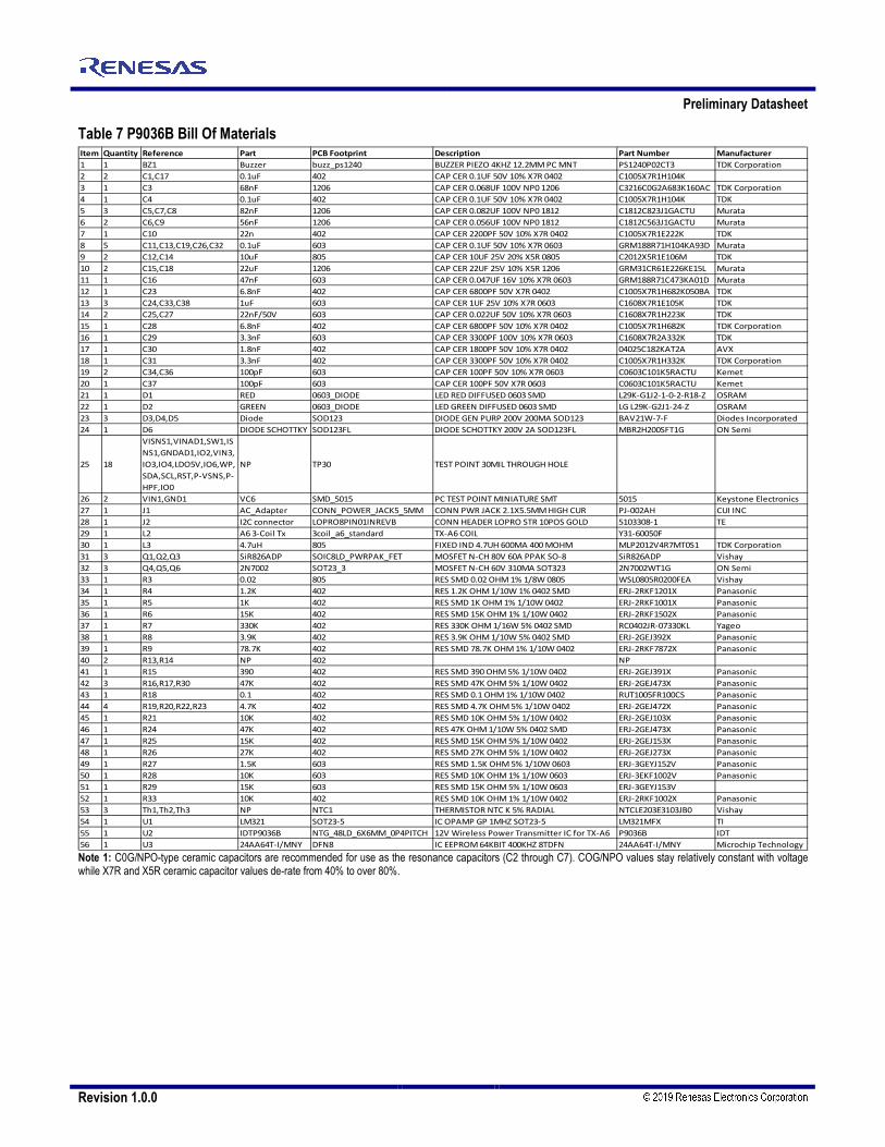
Table 7 P9036B Bill Of Materials Item Quantity Reference Part PCB Footprint Description Part Number Manufacturer1 1 BZ1 Buzzer buzz_ps1240 BUZZER PIEZO 4KHZ 12.2MM PC MNT PS1240P02CT3 TDK Corporation2 2 C1,C17 0.1uF 402 CAP CER 0.1UF 50V 10% X7R 0402 C1005X7R1H104K3 1 C3 68nF 1206 CAP CER 0.068UF 100V NP0 1206 C3216C0G2A683K160AC TDK Corporation4 1 C4 0.1uF 402 CAP CER 0.1UF 50V 10% X7R 0402 C1005X7R1H104K TDK5 3 C5,C7,C8 82nF 1206 CAP CER 0.082UF 100V NP0 1812 C1812C823J1GACTU Murata6 2 C6,C9 56nF 1206 CAP CER 0.056UF 100V NP0 1812 C1812C563J1GACTU Murata7 1 C10 22n 402 CAP CER 2200PF 50V 10% X7R 0402 C1005X7R1E222K TDK8 5 C11,C13,C19,C26,C32 0.1uF 603 CAP CER 0.1UF 50V 10% X7R 0603 GRM188R71H104KA93D Murata9 2 C12,C14 10uF 805 CAP CER 10UF 25V 20% X5R 0805 C2012X5R1E106M TDK10 2 C15,C18 22uF 1206 CAP CER 22UF 25V 10% X5R 1206 GRM31CR61E226KE15L Murata11 1 C16 47nF 603 CAP CER 0.047UF 16V 10% X7R 0603 GRM188R71C473KA01D Murata12 1 C23 6.8nF 402 CAP CER 6800PF 50V X7R 0402 C1005X7R1H682K050BA TDK13 3 C24,C33,C38 1uF 603 CAP CER 1UF 25V 10% X7R 0603 C1608X7R1E105K TDK14 2 C25,C27 22nF/50V 603 CAP CER 0.022UF 50V 10% X7R 0603 C1608X7R1H223K TDK15 1 C28 6.8nF 402 CAP CER 6800PF 50V 10% X7R 0402 C1005X7R1H682K TDK Corporation16 1 C29 3.3nF 603 CAP CER 3300PF 100V 10% X7R 0603 C1608X7R2A332K TDK17 1 C30 1.8nF 402 CAP CER 1800PF 50V 10% X7R 0402 04025C182KAT2A AVX18 1 C31 3.3nF 402 CAP CER 3300PF 50V 10% X7R 0402 C1005X7R1H332K TDK Corporation19 2 C34,C36 100pF 603 CAP CER 100PF 50V 10% X7R 0603 C0603C101K5RACTU Kemet20 1 C37 100pF 603 CAP CER 100PF 50V X7R 0603 C0603C101K5RACTU Kemet21 1 D1 RED 0603_DIODE LED RED DIFFUSED 0603 SMD L29K-G1J2-1-0-2-R18-Z OSRAM22 1 D2 GREEN 0603_DIODE LED GREEN DIFFUSED 0603 SMD LG L29K-G2J1-24-Z OSRAM23 3 D3,D4,D5 Diode SOD123 DIODE GEN PURP 200V 200MA SOD123 BAV21W-7-F Diodes Incorporated24 1 D6 DIODE SCHOTTKY SOD123FL DIODE SCHOTTKY 200V 2A SOD123FL MBR2H200SFT1G ON Semi
25 18
VISNS1,VINAD1,SW1,ISNS1,GNDAD1,IO2,VIN3,IO3,IO4,LDO5V,IO6,WP,SDA,SCL,RST,P-VSNS,P-HPF,IO0
NP TP30 TEST POINT 30MIL THROUGH HOLE
26 2 VIN1,GND1 VC6 SMD_5015 PC TEST POINT MINIATURE SMT 5015 Keystone Electronics27 1 J1 AC_Adapter CONN_POWER_JACK5_5MM CONN PWR JACK 2.1X5.5MM HIGH CUR PJ-002AH CUI INC28 1 J2 I2C connector LOPRO8PIN01INREVB CONN HEADER LOPRO STR 10POS GOLD 5103308-1 TE29 1 L2 A6 3-Coil Tx 3coil_a6_standard TX-A6 COIL Y31-60050F30 1 L3 4.7uH 805 FIXED IND 4.7UH 600MA 400 MOHM MLP2012V4R7MT0S1 TDK Corporation31 3 Q1,Q2,Q3 SiR826ADP SOIC8LD_PWRPAK_FET MOSFET N-CH 80V 60A PPAK SO-8 SiR826ADP Vishay32 3 Q4,Q5,Q6 2N7002 SOT23_3 MOSFET N-CH 60V 310MA SOT323 2N7002WT1G ON Semi33 1 R3 0.02 805 RES SMD 0.02 OHM 1% 1/8W 0805 WSL0805R0200FEA Vishay34 1 R4 1.2K 402 RES 1.2K OHM 1/10W 1% 0402 SMD ERJ-2RKF1201X Panasonic35 1 R5 1K 402 RES SMD 1K OHM 1% 1/10W 0402 ERJ-2RKF1001X Panasonic36 1 R6 15K 402 RES SMD 15K OHM 1% 1/10W 0402 ERJ-2RKF1502X Panasonic37 1 R7 330K 402 RES 330K OHM 1/16W 5% 0402 SMD RC0402JR-07330KL Yageo38 1 R8 3.9K 402 RES 3.9K OHM 1/10W 5% 0402 SMD ERJ-2GEJ392X Panasonic39 1 R9 78.7K 402 RES SMD 78.7K OHM 1% 1/10W 0402 ERJ-2RKF7872X Panasonic40 2 R13,R14 NP 402 NP41 1 R15 390 402 RES SMD 390 OHM 5% 1/10W 0402 ERJ-2GEJ391X Panasonic42 3 R16,R17,R30 47K 402 RES SMD 47K OHM 5% 1/10W 0402 ERJ-2GEJ473X Panasonic43 1 R18 0.1 402 RES SMD 0.1 OHM 1% 1/10W 0402 RUT1005FR100CS Panasonic44 4 R19,R20,R22,R23 4.7K 402 RES SMD 4.7K OHM 5% 1/10W 0402 ERJ-2GEJ472X Panasonic45 1 R21 10K 402 RES SMD 10K OHM 5% 1/10W 0402 ERJ-2GEJ103X Panasonic46 1 R24 47K 402 RES 47K OHM 1/10W 5% 0402 SMD ERJ-2GEJ473X Panasonic47 1 R25 15K 402 RES SMD 15K OHM 5% 1/10W 0402 ERJ-2GEJ153X Panasonic48 1 R26 27K 402 RES SMD 27K OHM 5% 1/10W 0402 ERJ-2GEJ273X Panasonic49 1 R27 1.5K 603 RES SMD 1.5K OHM 5% 1/10W 0603 ERJ-3GEYJ152V Panasonic50 1 R28 10K 603 RES SMD 10K OHM 1% 1/10W 0603 ERJ-3EKF1002V Panasonic51 1 R29 15K 603 RES SMD 15K OHM 5% 1/10W 0603 ERJ-3GEYJ153V52 1 R33 10K 402 RES SMD 10K OHM 1% 1/10W 0402 ERJ-2RKF1002X Panasonic53 3 Th1,Th2,Th3 NP NTC1 THERMISTOR NTC K 5% RADIAL NTCLE203E3103JB0 Vishay54 1 U1 LM321 SOT23-5 IC OPAMP GP 1MHZ SOT23-5 LM321MFX TI55 1 U2 IDTP9036B NTG_48LD_6X6MM_0P4PITCH 12V Wireless Power Transmitter IC for TX-A6 P9036B IDT56 1 U3 24AA64T-I/MNY DFN8 IC EEPROM 64KBIT 400KHZ 8TDFN 24AA64T-I/MNY Microchip Technology
Note 1: C0G/NPO-type ceramic capacitors are recommended for use as the resonance capacitors (C2 through C7). COG/NPO values stay relatively constant with voltage while X7R and X5R ceramic capacitor values de-rate from 40% to over 80%.
Revision 1.0.0 19
P9036B Product Datasheet
External Components The P9036B requires a minimum number of external components for proper operation (see the BOM in Table 7). A complete design schematic compliant to the WPC “Qi” standard is given in Figure 7. It includes WPC “Qi” LED signaling, buzzer, and an EEPROM for loading P9036B firmware.
I2C Communication The P9036B includes an I2C block which can support either I2C Master or I2C Slave operation. After power-on-reset (POR),the P9036B will initially acts as an I2C Master for the purpose of downloading firmware from an external memory device, such as an EEPROM. The I2C Master mode on the P9036B does not support multi-master mode, and it is important for system designers to avoid any bus master conflict until the P9036B has finished any firmware uploading and has released control of the bus as I2C Master. After firmware downloaded from external memory is complete, and when the P9036B begins normal operation, the P9036B is configured by the standard firmware to be exclusively in I2C Slave mode.
EEPROM The P9036B EVK supports an external EEPROM memory chip,pre-programmed with a standard operating firmware that is automatically loaded when 5V power is applied. The P9036B uses I2C master address 0x52 to access the EEPROM. The P9036B slave address is 0x39. If the standard firmware is not suitable for the application, a custom EEPROM or internal factory programmed ROM is possible. For future flexibility, the P9036B will first sequentially try to communicate with the EEPROM first using address 0x50, then 0x52, and finally 0x54. Each address supports a different formatting of the EEPROM data. At this time, the only supported format is at address 0x52. When the P9036B receives a response from the EEPROM, the
sequencing will stop and the P9036B will use the firmware that is up loaded from that address.
Overview of Standard GPIO Usage There are 7 GPIO’s on the P9036B transmitter IC, of which two are available for use as follows:
• GPIO0,2,6: Selects one of the three available coils.• GPIO1,5: Manages the demodulation signal selection.• GPIO3: Green LED and external resistors for
choosing LED mode.• GPIO4: Red LED and AC or DC buzzer (optional) and
external resistors for choosing FOD offset option.Table 8 table lists how the red and green LEDs can be used to display information about the P9036B’s operating modes. The table also includes information about external resistors or internal pull up/down options to select LED modes.
LED FUNCTIONS Two GPIOs are used to drive LEDs, which indicate, through various on/off and illumination options, the state of charging and some possible fault conditions.
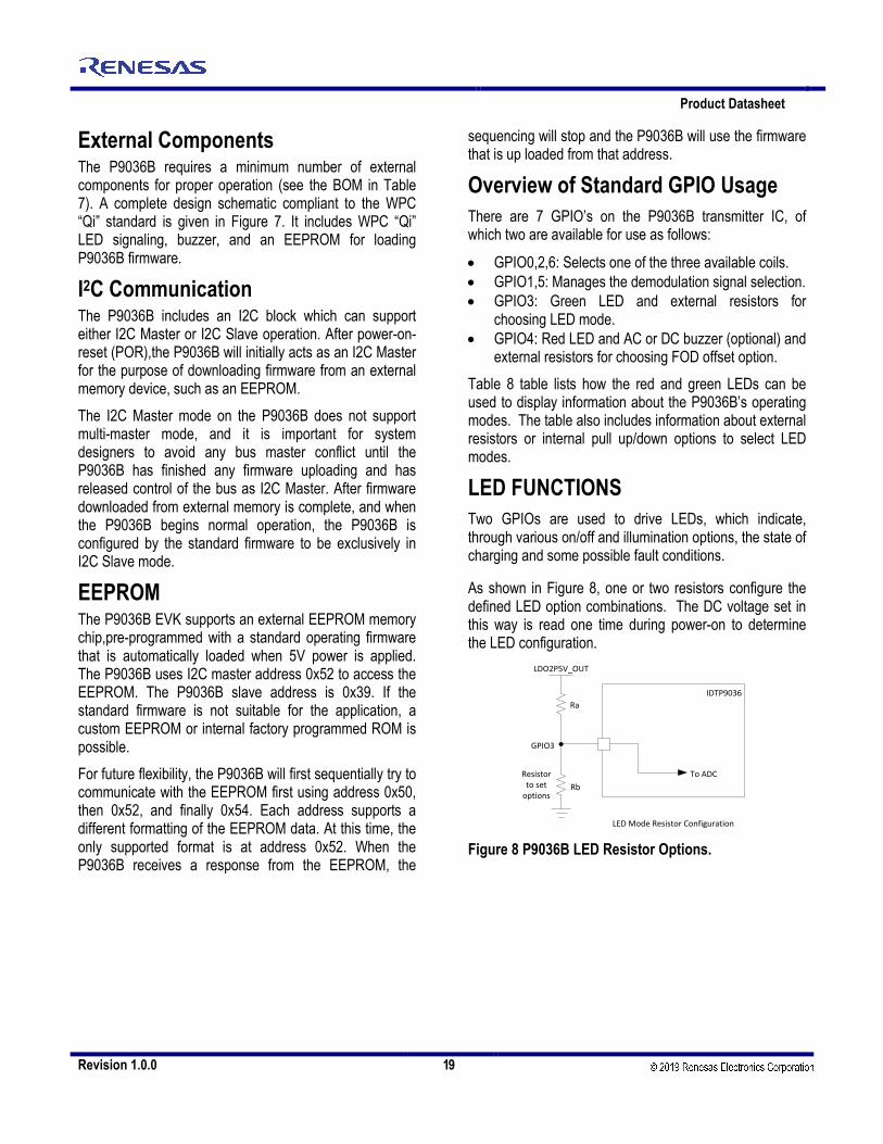
As shown in Figure 8, one or two resistors configure the defined LED option combinations. The DC voltage set in this way is read one time during power-on to determine the LED configuration.
IDTP9036
To ADC
Ra
Rb
LDO2P5V_OUT
GPIO3
Resistorto set
options
LED Mode Resistor Configuration
Figure 8 P9036B LED Resistor Options.

P9036B Product Datasheet
Revision 1.0.0 20 © 2016 Integrated Device Technology, Inc.
Table 8 – P9036B LED Functions
Standby Transfer Complete CS100 Low-Power FaultLED1- Green On Blink 1Hz On Blink 0.5Hz Blink 2Hz OFF
LED2- Red On Off Off Off Off Blink 4HzLED1- Green On On Off Blink 0.5Hz Blink 2Hz OFF
LED2- Red On Off Off Off Off Blink 4HzLED1- Green Off Blink 1Hz On Blink 0.5Hz Blink 2Hz Blink 4Hz
LED2- n/a - - - - - -LED1- Green Off On Off Blink 0.5Hz Blink 2Hz Blink 4Hz
LED2- n/a - - - - - -LED1- Green Off On Off Blink 0.5Hz Blink 2Hz Off
LED2- Red Off Off Off Off Off Blink 4HzLED1- Green Off Off On Off Off Off
LED2- Red Off On Off Blink 0.5Hz Blink 2Hz Blink 4HzLED1- Green
LED2- RedLED1- Green
LED2- RedLED1- Green
LED2- RedLED1- Green Off Blink 1Hz On Blink 0.5Hz Blink 2Hz Off
LED2- Red Off Off Off Off Off Blink 4HzNote 1 - Voltage divider on GPIO3 should use 1% resistors with parallel impedance approximately 20k-50k. CS100 is indicated when Rx sends "Charge Status 100" message. Normal indication resumes after Rx sends "Charge Status 90" or less.CS100 Blink is approximately 68% on-time"Low Power" is indicated in USB powered applications when USB does not provide sufficient DC power"Low Power" Blink is approximately 80% on-timeNote 2 - LED Select voltage should be within ±3% of listed value.
LED ControlOption
LED SelectGPIO3 Voltage Description
LED #/Color
Operational Status
Dual LED, Standby - OnNo-Blink
Single-LED, Standby OFFBlink
Single-LED, Standby OFFNo Blink
Dual LED, Standby - OffNo-Blink
Reserved
Reserved
1.000V
0.810V
1.100V
1.250V
Reserved
Dual LED, Standby - OffRed Indicate, No-Blink
Dual-LED, Standby - OffBlink
Dual-LED, Standby - OnBlink
3
4
5
2
7
6
8
9Pull Up
>=1.500V
Pull Down<=0.080V
10
1
0.370V
0.510V
0.660V
0.220V
Buzzer Function An optional buzzer feature is supported on GPIO4 which is able to drive directly a piezoelectric type transducer without amplification. As shown on the reference schematic, a series current limiting resistor should be included if a buzzer device is included. The buzzer signal is approximately a 2kHz square wave, and it is recommended to use a buzzer with a 2kHz resonant frequency for best results. Buzzer Action: Power Transfer Indication The P9036B supports audible notification when the device operation successfully reaches the Power Transfer state. The duration of the Power Transfer indication sound is approximately 200ms. Buzzer Action: Charge Complete Indication
The P9036B supports audible notification when the receiver sends a "Charge Complete" during the power transfer state. If "Charge Complete" is sent as the very first packet before being in the power transfer state, there is no buzzer indication for this case. The duration of the “Charge Complete” indication sound is approximately 200ms.
Decoupling/Bulk Capacitors As with any high-performance mixed-signal IC, the P9036B must be isolated from the system power supply noise to perform optimally. A decoupling capacitor of 0.1μF must be connected between each power supply and the PCB ground plane as close to these pins as possible. For optimum device performance, the decoupling capacitor must be mounted on the component side of the PCB. Additionally, medium value capacitors in the 22μF

Revision 1.0.0 21
P9036B Product Datasheet
range must be used at the VIN inputs (IN,IN1,IN2) to minimize ripple current and voltage droop due to the large current requirements of the resonant half Half-Bridge driver. The value of the capacitors will decrease as the voltage applied approaches the nominal voltage, due to the ceramic dielectric characteristics. For example, a 22μF X7R 25V capacitor’s value could be as low as 6μF when operating at 13V, depending on the manufacturer.
WPC TX-A6 Coil The internal half-bridge output connects to three series-resonance circuits made by a WPC triple Type-A6 coil and series resonant capacitors. The selected inductor serves as the primary coil of a loosely-coupled transformer, the secondary of which is the inductor connected to the power receiver.
Resonance Capacitors The resonance capacitors must be C0G type dielectric and have a DC rating of at least 100V. The part numbers are shown in the Bill Of Materials
Buck Converter The input capacitors (CIN) must be connected directly between the power pins (REG_IN and BUCK5VT_IN) and power PGND pins as near as possible to the IC pins. The output capacitor (COUT) must be placed as close to the device and power ground pins (PGND) as possible.
The output-sense connection to the feedback pin, BUCK5VT_SNS, must be separated from any power trace. Connect the output-sense trace as close as possible to the load point to avoid additional load regulation errors. The power traces, including PGND traces, the LX or 5V output traces, and the VIN trace must be kept short, direct and wide to allow large current flow. Use several via pads when routing power lines between layers.
LDOs Input Capacitor The input capacitors must be located as physically close as possible to the power pin (LDO2P5V_IN) and power ground (GND). Ceramic capacitors are recommended for their low ESR and small profile. Typically, 10V- or 16V-rated capacitors are recommended.
Output Capacitor For proper voltage regulation and stability, a capacitor is required on the output of each LDO (LDO2P5V and LDO5V). The output capacitor must be placed as close to the device and power (PGND) pins as possible. Since the LDOs have been designed to function with very low ESR capacitors, a ceramic capacitor is reuqired for best performance.
PCB Layout Considerations
- For optimum device performance and lowest outputphase noise, the following guidelines must beobserved. Please contact IDT for Gerber files thatcontain the recommended board layout.
- As for all switching power supplies, especially thoseproviding high current and using high switchingfrequencies, layout is an important design step. Iflayout is not carefully done, the regulator could showinstability as well as EMI problems. Therefore, usewide and short traces for high current paths. If thereare any uncertainties regarding best layout practicesit is best to follow the provided, optimized IDT layout.
- The 0.1μF decoupling capacitors must be mounted onthe component side of the board as close as possibleto the pins intended to be decoupled. Keep PCBtraces to each power pin and to ground vias as shortas possible.
- To optimize board layout, place all components onthe same side of the board.
- All passive components in the network connecting tothe HPF pin, up to and including the three smallsignal diodes must be placed close to the HPF pin.This is a high sensitivity analog circuit, and traceswith high voltage or high noise must be routed awayfrom this area. It is especially important to mount thecapacitor connecting to the HPF pin as close aspossible to the HPF pin. Additionally, the HPF pin is ahigh impedance input and any DC leakage into thisnode can reduce performance.

P9036B Product Datasheet
Revision 1.0.0 22 © 2016 Integrated Device Technology, Inc.
- The NQG48 6.0mm x 6.0mm x 0.75mm 48L packagehas an inner thermal pad, which requires blindassembly. It is recommended that a more active fluxsolder paste be used such as Alpha OM-350 solderpaste from Cookson Electronics(http://www.cooksonsemi.com). Please contact IDTfor Gerber files that contain recommended solderstencil design.
- The package center exposed pad (EP) must bereliably soldered directly to the PCB. The center landpad on the PCB must also be tied to the board groundplane, primarily to maximize thermal performance inthe application. The ground connection is bestachieved using a matrix of plated-through-hole (PTH)vias embedded in the PCB center land pad for theNTG48. The PTH vias perform as thermal conduits tothe ground plane (thermally, a heat spreader) fromthe solder side of the board.
- On the solder side of the board, these thermal viasembed in a copper fill having the same dimensions asthe center land pad on the component side.Recommendations for the via finished hole-size andarray pitch are 0.3mm to 0.33mm and 1.3mm,respectively.
Power Dissipation/Thermal Requirements The P9036B is offered in a TQFN-48L package. The maximum power dissipation capability is 1.3W, limited by the die’s specified maximum operating junction temperature, TJ, of 125°C. The junction temperature rises with the device power dissipation based on the package thermal resistance. The package offers a typical thermal resistance, junction to ambient (θJA), of 31°C/W when the PCB layout and surrounding devices are optimized as described in the PCB Layout Considerations section. The techniques as noted in the PCB Layout section need to be followed when designing the printed circuit board layout. Care should be exercised to avoid the placement of the P9036B IC package in proximity to other heat generating devices in a given application design. The ambient temperature around the power IC will also have an effect on the thermal limits of an application. The overall goal is to have as much uninterrupted copper material on both the top and bottom layers of the PCB to carry away heat away for the P9036B as quickly as possible.
Special Notes NQG TQFN-48 Package Assembly Note 1: Unopened Dry Packaged Parts have a one year shelf life. Note 2: The HIC indicator card for newly opened Dry Packaged Parts should be checked. If there is any moisture content, the parts must be baked for a minimum of 8 hours at 125˚C within 24 hours of the assembly reflow process.

Revision 1.0.0 23
P9036B Product Datasheet
PACKAGE OUTLINE DRAWING
Figure 9 P9036B Package Outline Drawing (NTG48 TQFN-48L 6.0 mm x 6.0 mm x 0.75 mm48L, 0.4mm pitch)

P9036B Product Datasheet
ORDERING GUIDE Table 9 Ordering Summary
PART NUMBER MARKING PACKAGE AMBIENT TEMP. RANGE
SHIPPING CARRIER QUANTITY
P9036BNTGI P9036BNTG NTG48 - TQFN-48 6x6x0.75mm -40°C to +85°C Tray 25 P9036BNTGI8 P9036BNTG NTG48 - TQFN-48 6x6x0.75mm -40°C to +85°C Tape and Reel 2,500

Corporate HeadquartersTOYOSU FORESIA, 3-2-24 Toyosu,Koto-ku, Tokyo 135-0061, Japanwww.renesas.com
Contact InformationFor further information on a product, technology, the most up-to-date version of a document, or your nearest sales office, please visit:www.renesas.com/contact/
TrademarksRenesas and the Renesas logo are trademarks of Renesas Electronics Corporation. All trademarks and registered trademarks are the property of their respective owners.
IMPORTANT NOTICE AND DISCLAIMER
RENESAS ELECTRONICS CORPORATION AND ITS SUBSIDIARIES (“RENESAS”) PROVIDES TECHNICAL SPECIFICATIONS AND RELIABILITY DATA (INCLUDING DATASHEETS), DESIGN RESOURCES (INCLUDING REFERENCE DESIGNS), APPLICATION OR OTHER DESIGN ADVICE, WEB TOOLS, SAFETY INFORMATION, AND OTHER RESOURCES “AS IS” AND WITH ALL FAULTS, AND DISCLAIMS ALL WARRANTIES, EXPRESS OR IMPLIED, INCLUDING, WITHOUT LIMITATION, ANY IMPLIED WARRANTIES OF MERCHANTABILITY, FITNESS FOR A PARTICULAR PURPOSE, OR NON-INFRINGEMENT OF THIRD PARTY INTELLECTUAL PROPERTY RIGHTS.
These resources are intended for developers skilled in the art designing with Renesas products. You are solely responsible for (1) selecting the appropriate products for your application, (2) designing, validating, and testing your application, and (3) ensuring your application meets applicable standards, and any other safety, security, or other requirements. These resources are subject to change without notice. Renesas grants you permission to use these resources only for development of an application that uses Renesas products. Other reproduction or use of these resources is strictly prohibited. No license is granted to any other Renesas intellectual property or to any third party intellectual property. Renesas disclaims responsibility for, and you will fully indemnify Renesas and its representatives against, any claims, damages, costs, losses, or liabilities arising out of your use of these resources. Renesas' products are provided only subject to Renesas' Terms and Conditions of Sale or other applicable terms agreed to in writing. No use of any Renesas resources expands or otherwise alters any applicable warranties or warranty disclaimers for these products.
(Rev.1.0 Mar 2020)
© 2020 Renesas Electronics Corporation. All rights reserved.