12_chapter6
12
Chapter 6 Design of Voltage Controlled Oscillator (VCO) Using 45nm VLSI Technology 79 CHAPTER 6 DESIGN OF VOLTAGE CONTROLLED OSCILLATOR (VCO) USING 45 NM VLSI TECHNOLOGY Oscillators are required to generate the carrying signals for radio frequency transmission, but also for the main clocks of processors. The ring oscillator is a very simple oscillator circuit, based on the switching delay existing between the input and output of an inverter. VCOs are generally of the form of a ring oscillator, relaxation oscillator or a resonant oscillator. The ring oscillator, common in monolithic topologies takes the form of an odd number of inverters connected in a feedback loop. If we connect an odd chain of inverters, we obtain a natural oscillation, with a period which corresponds roughly to number of elementary delays per gate. 5 stage ring oscillator is shown in fig 6.1 below. Fig 6.1. A ring oscillator is based on odd number of inverters
-
Upload
maheshsamanapally -
Category
Documents
-
view
221 -
download
0
Transcript of 12_chapter6

Chapter 6 Design of Voltage Controlled Oscillator (VCO) Using 45nm VLSI Technology 79
CHAPTER 6
DESIGN OF VOLTAGE CONTROLLED OSCILLATOR (VCO)
USING 45 NM VLSI TECHNOLOGY
Oscillators are required to generate the carrying signals for radio frequency
transmission, but also for the main clocks of processors. The ring oscillator is a very
simple oscillator circuit, based on the switching delay existing between the input and
output of an inverter. VCOs are generally of the form of a ring oscillator, relaxation
oscillator or a resonant oscillator. The ring oscillator, common in monolithic topologies
takes the form of an odd number of inverters connected in a feedback loop.
If we connect an odd chain of inverters, we obtain a natural oscillation, with a
period which corresponds roughly to number of elementary delays per gate. 5 stage ring
oscillator is shown in fig 6.1 below.
Fig 6.1. A ring oscillator is based on odd number of inverters

Chapter 6 Design of Voltage Controlled Oscillator (VCO) Using 45nm VLSI Technology 80
The voltage controlled oscillator (VCO) generates a clock with a controllable
frequency. The VCO is commonly used for clock generation in phase lock loop circuits.
The clock may vary typically by +/-50% of its central frequency. A current-starved
voltage controlled oscillator is shown in fig 6.2.
The current-started inverter chain uses a voltage control Vcontrol to modify the
current that flows in the N1, P1 branch. The current through N1 is mirrored by N2, N3,
N4, N5 & N6. The some current flows in P1. The current Through P1 is mirrored by P2,
P3 and P4. Consequent by the change in Vcontrol induces a global change in the inverter
currents and acts directly on the delay.
Fig 6.2. Schematic diagram of a voltage controlled oscillator
The Voltage Controlled Oscillator required for PLL should posses following
characteristics:
i) The oscillating frequency should be restricted to the required bandwidth. For
example, in European mobile phone applications, the VCO frequency should
be varying between flow = 1700 MH2 and High=1800 MH2.

Chapter 6 Design of Voltage Controlled Oscillator (VCO) Using 45nm VLSI Technology 81
ii) Due to process variations, the VCO frequency range should be extended to
fmin, fmax, typically 10% higher and lower than the request range.
iii) When the control voltage Vc is equal to VDD/2, the clock should be centered
in the middle of the desired frequency range.
iv) The duty cycle of VCO clock output should be as close as possible to 50%. If
this is not the case, the PLL would have problems locking, or would not
produce a stable output clock.
The implementation of the current starved for a five inverter chain using, 45nm
VLSI technology is shown in following fig 6.3.Technology used is CMOS 45 nm,
High/k/metal/strain-8 metal copper (1.00, 1.8v). In the layout the current mirror is situated
in the left. Five inverters have been designed to create the basic ring oscillator. The buffer
inverter is situated on the right side of the layout, through which output Vhigh is taken.
The supply VDD is chosen as 1.00 Volt DC supply. Vcontrol is the clock applied
with low time (tl) = 0.225 ns, Rise time (tr) = 10 ns, High time (th) = 0.225 ns and full
time (tf )= 10 ns.Vss is DC supply of 0.0V. NMOS transistor is having the width W =
0.120 µm and length L = 0.040 µm. The total power consumption of the circuit is P =
16.076 µw.
The fig 6.3 shows layout for VCO. Fig 6.4 shows voltage and currents with respect
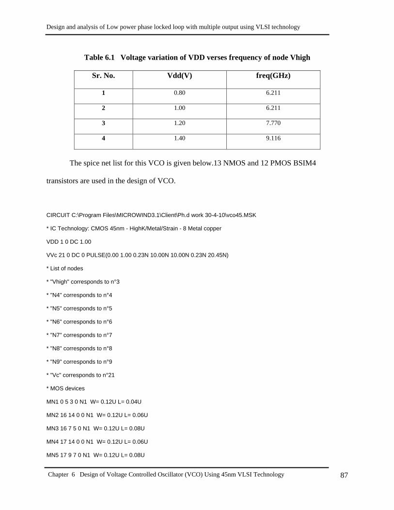
to time. The output frequency Vhigh of VCO is shown in fig 6.5. From the data array
shown in graph in fig 6.6 and as shown in table 6.1, it is found that frequency remain same
i.e. 6.21 GHz upto 1.0 volt. As the supply voltage increases beyond 1.0 volt frequency get
varied.

Chapter 6 Design of Voltage Controlled Oscillator (VCO) Using 45nm VLSI Technology 82
Simulation of VCO layout is taken for frequency Vs time graph with timescale of
5nsec. The frequency obtained for VCO is 6.21 GHz. By increasing the no. of inverter
and altering the size of the MOS current source, we may modify the oscillating frequency
very easily.

Chapter 6 Design of Voltage Controlled Oscillator (VCO) Using 45nm VLSI Technology
83
Fig
6.3
l
ayou
t of
volt
age
con
troll
ed o
scil
lato
r u
sin
g 4
5n
m V
LS
I te
chn
olo
gy

Chapter 6 Design of Voltage Controlled Oscillator (VCO) Using 45nm VLSI Technology
84
Fig
6.4
V
olt
age
an
d c
urr
ents
o
f V
CO
wit
h r
esp
ect
to t
ime

Chapter 6 Design of Voltage Controlled Oscillator (VCO) Using 45nm VLSI Technology
85
Fig
6.5
Ou
tpu
t fr
equ
ency
of
VC
O v
erse
s ti
me

Chapter 6 Design of Voltage Controlled Oscillator (VCO) Using 45nm VLSI Technology
86
Fig
6.6
Volt
age
vari
ati
on
of
VD
D v
erse
s fr
equ
ency
of
nod
e V
hig
h
Design and analysis of Low power phase locked loop with multiple output using VLSI technology
Chapter 6 Design of Voltage Controlled Oscillator (VCO) Using 45nm VLSI Technology
87
Table 6.1 Voltage variation of VDD verses frequency of node Vhigh
Sr. No. Vdd(V) freq(GHz)
1 0.80
6.211
2 1.00
6.211
3 1.20 7.770
4 1.40
9.116
The spice net list for this VCO is given below.13 NMOS and 12 PMOS BSIM4
transistors are used in the design of VCO.
CIRCUIT C:\Program Files\MICROWIND3.1\Client\Ph.d work 30-4-10\vco45.MSK
* IC Technology: CMOS 45nm - HighK/Metal/Strain - 8 Metal copper
VDD 1 0 DC 1.00
VVc 21 0 DC 0 PULSE(0.00 1.00 0.23N 10.00N 10.00N 0.23N 20.45N)
* List of nodes
* "Vhigh" corresponds to n°3
* "N4" corresponds to n°4
* "N5" corresponds to n°5
* "N6" corresponds to n°6
* "N7" corresponds to n°7
* "N8" corresponds to n°8
* "N9" corresponds to n°9
* "Vc" corresponds to n°21
* MOS devices
MN1 0 5 3 0 N1 W= 0.12U L= 0.04U
MN2 16 14 0 0 N1 W= 0.12U L= 0.06U
MN3 16 7 5 0 N1 W= 0.12U L= 0.08U
MN4 17 14 0 0 N1 W= 0.12U L= 0.06U
MN5 17 9 7 0 N1 W= 0.12U L= 0.08U

Design and analysis of Low power phase locked loop with multiple output using VLSI technology
Chapter 6 Design of Voltage Controlled Oscillator (VCO) Using 45nm VLSI Technology
88
MN6 18 14 0 0 N1 W= 0.12U L= 0.06U
MN7 18 11 9 0 N1 W= 0.12U L= 0.08U
MN8 19 14 0 0 N1 W= 0.12U L= 0.06U
MN9 19 13 11 0 N1 W= 0.12U L= 0.08U
MN10 20 14 0 0 N1 W= 0.12U L= 0.06U
MN11 20 9 13 0 N1 W= 0.12U L= 0.08U
MN12 0 14 14 0 N1 W= 0.12U L= 0.08U
MN13 0 21 14 0 N1 W= 0.08U L= 0.22U
MP1 1 5 3 1 P1 W= 0.30U L= 0.04U
MP2 1 14 4 1 P1 W= 0.30U L= 0.06U
MP3 4 7 5 1 P1 W= 0.28U L= 0.08U
MP4 1 14 6 1 P1 W= 0.30U L= 0.06U
MP5 6 9 7 1 P1 W= 0.28U L= 0.08U
MP6 1 14 8 1 P1 W= 0.30U L= 0.06U
MP7 8 11 9 1 P1 W= 0.28U L= 0.08U
MP8 1 14 10 1 P1 W= 0.30U L= 0.06U
MP9 10 13 11 1 P1 W= 0.28U L= 0.08U
MP10 1 14 12 1 P1 W= 0.30U L= 0.06U
MP11 12 9 13 1 P1 W= 0.28U L= 0.08U
MP12 1 14 14 1 P1 W= 0.30U L= 0.08U
C2 1 0 1.708fF
C3 3 0 0.207fF
C4 4 0 0.220fF
C5 5 0 0.197fF
C6 6 0 0.231fF
C7 7 0 0.196fF
C8 8 0 0.220fF
C9 9 0 0.285fF
C10 10 0 0.231fF
C11 11 0 0.196fF
C12 12 0 0.205fF

Design and analysis of Low power phase locked loop with multiple output using VLSI technology
Chapter 6 Design of Voltage Controlled Oscillator (VCO) Using 45nm VLSI Technology
89
C13 13 0 0.181fF
C14 14 0 0.283fF
C16 16 0 0.124fF
C17 17 0 0.124fF
C18 18 0 0.124fF
C19 19 0 0.124fF
C20 20 0 0.124fF
C21 21 0 0.013fF
* n-MOS BSIM4 :
* low leakage
.MODEL N1 NMOS LEVEL=14 VTHO=0.19 U0=0.020 TOXE= 3.5E-9 LINT=0.000U
+K1 =0.750 K2=0.100 DVT0=2.300
+DVT1=0.540 LPE0=2.200e-9 ETA0=0.080
+NFACTOR= 0.1 U0=0.020 UA=6.300e-15
+WINT=0.020U LPE0=2.200e-9
+KT1=-0.060 UTE=-1.800 VOFF=0.000
+XJ=0.150U NDEP=170.000e15 PCLM=1.100
+CGSO=100.0p CGDO=100.0p
+CGBO= 60.0p
* p-MOS BSIM4:
* low leakage
.MODEL P1 PMOS LEVEL=14 VTHO=-0.15 U0=0.018 TOXE= 3.5E-9 LINT=0.000U
+K1 =0.650 K2=0.100 DVT0=2.300
+DVT1=0.540 LPE0=2.200e-9 ETA0=0.080
+NFACTOR= 0.1 U0=0.018 UA=9.500e-15
+WINT=0.020U LPE0=2.200e-9
+KT1=-0.060 UTE=-1.800 VOFF=0.000
+XJ=0.150U NDEP=170.000e15 PCLM=0.700
+CGSO=100.0p CGDO=100.0p
+CGBO= 60.0p
* Transient analysis

Design and analysis of Low power phase locked loop with multiple output using VLSI technology
Chapter 6 Design of Voltage Controlled Oscillator (VCO) Using 45nm VLSI Technology
90
** (Pspice)
.TEMP 27.0
.TRAN 0.1N 10.00N
.PROBE
.END