10K - 40K Gates C of AT40K FPGA with 8-bit Microcontroller ...
130
Features • Monolithic Field Programmable System Level Integrated Circuit – AT40K SRAM-based FPGA with Embedded High-performance RISC AVR ® Core and Extensive Data and Instruction SRAM • 10,000 to 40,000 Gates of Patented SRAM-based AT40K FPGA with FreeRAM ™ – 4.6K - 18.4K Bits of Distributed Single/Dual Port FPGA User SRAM – High-performance DSP Optimized FPGA Core Cell – Dynamically Reconfigurable In-System – FPGA Configuration Access Available On-chip from AVR Microcontroller Core to Support Cache Logic ® Designs – Very Low Static and Dynamic Power Consumption – Ideal for Portable and Handheld Applications • Patented AVR Enhanced RISC Architecture – 120+ Powerful Instructions – Most Single Clock Cycle Execution – High-performance Hardware Multiplier for DSP-based Systems – Over 30 MIPS Performance Available – “C” Code Optimized Architecture with 32 x 8 General Purpose Internal Registers – Low-power Idle, Power-save, and Power-down Modes • 36K Bytes of Dynamically Allocated Instruction and Data SRAM – Up to 16K x 16 Internal 15 ns Instructions SRAM – Up to 16K x 8 Internal 15 ns Data SRAM • AVR Fixed Peripherals – Industry-standard two-wire Interface – Two Programmable Serial UARTs – Two 8-bit Timer/Counters with Separate Prescaler and PWM – One 16-bit Timer/Counter with Separate Prescaler, Compare, Capture Modes and Dual 8-, 9-, or 10-bit PWM • Support for FPGA Custom Peripherals – AVR Peripheral Control – 16 Decoded AVR Address Lines Directly Accessible to FPGA – FPGA Macro Library of Custom Peripherals • 16 FPGA Supplied Internal Interrupts to AVR • Up to 4 External Interrupts to AVR • 8 Global FPGA Clocks – Two FPGA Clocks Driven from AVR Logic – FPGA Global Clock Access Available from FPGA Core • Multiple Oscillator Circuits – Programmable Watchdog Timer with On-chip Oscillator – Oscillator to AVR Internal Clock Circuit – Software-selectable Clock Frequency – Oscillator to Timer/Counter for Real-time Clock • V CC : 3.0V - 3.6V • 3.3V 33 MHz PCI Compliant FPGA I/O – 24 mA Sink/Source High-performance I/O Structures – All FPGA I/O Individually Programmable • Pin-compatible with the Atmel AT40K Series FPGAs • High-performance, Low-power 0.35μ CMOS five Layer Metal Process • State-of-the-art Integrated PC-based Software Suite including Co-verification Description The AT94K Series (FPSLIC family) shown in Table 1 is a combination of the popular Atmel AT40K series SRAM FPGAs and the high-performance Atmel AVR 8-bit RISC microcontroller with standard peripherals. Extensive data and instruction SRAM as well as device control and management logic are included on this monolithic device, fabricated on Atmel’s 0.35μ five-layer metal CMOS process. Rev. 1138B–12/99 10K - 40K Gates of AT40K FPGA with 8-bit Microcontroller and 36K Bytes of SRAM AT94K Series Field Programmable System Level Integrated Circuit Advance Information (continued)
Transcript of 10K - 40K Gates C of AT40K FPGA with 8-bit Microcontroller ...

Rev. 1138B–12/99
10K - 40K Gates of AT40K FPGA with 8-bitMicrocontroller and 36K Bytes of SRAM
AT94K Series Field Programmable System LevelIntegrated Circuit
Advance Information
Features• Monolithic Field Programmable System Level Integrated Circuit
– AT40K SRAM-based FPGA with Embedded High-performance RISC AVR® Core and Extensive Data and Instruction SRAM
• 10,000 to 40,000 Gates of Patented SRAM-based AT40K FPGA with FreeRAM™
– 4.6K - 18.4K Bits of Distributed Single/Dual Port FPGA User SRAM– High-performance DSP Optimized FPGA Core Cell– Dynamically Reconfigurable In-System – FPGA Configuration Access Available
On-chip from AVR Microcontroller Core to Support Cache Logic® Designs– Very Low Static and Dynamic Power Consumption – Ideal for Portable and
Handheld Applications• Patented AVR Enhanced RISC Architecture
– 120+ Powerful Instructions – Most Single Clock Cycle Execution– High-performance Hardware Multiplier for DSP-based Systems– Over 30 MIPS Performance Available– “C” Code Optimized Architecture with 32 x 8 General Purpose Internal Registers– Low-power Idle, Power-save, and Power-down Modes
• 36K Bytes of Dynamically Allocated Instruction and Data SRAM– Up to 16K x 16 Internal 15 ns Instructions SRAM– Up to 16K x 8 Internal 15 ns Data SRAM
• AVR Fixed Peripherals– Industry-standard two-wire Interface– Two Programmable Serial UARTs– Two 8-bit Timer/Counters with Separate Prescaler and PWM– One 16-bit Timer/Counter with Separate Prescaler, Compare, Capture
Modes and Dual 8-, 9-, or 10-bit PWM• Support for FPGA Custom Peripherals
– AVR Peripheral Control – 16 Decoded AVR Address Lines Directly Accessible to FPGA
– FPGA Macro Library of Custom Peripherals• 16 FPGA Supplied Internal Interrupts to AVR • Up to 4 External Interrupts to AVR• 8 Global FPGA Clocks
– Two FPGA Clocks Driven from AVR Logic– FPGA Global Clock Access Available from FPGA Core
• Multiple Oscillator Circuits– Programmable Watchdog Timer with On-chip Oscillator– Oscillator to AVR Internal Clock Circuit– Software-selectable Clock Frequency– Oscillator to Timer/Counter for Real-time Clock
• VCC: 3.0V - 3.6V• 3.3V 33 MHz PCI Compliant FPGA I/O
– 24 mA Sink/Source High-performance I/O Structures– All FPGA I/O Individually Programmable
• Pin-compatible with the Atmel AT40K Series FPGAs• High-performance, Low-power 0.35µ CMOS five Layer Metal Process• State-of-the-art Integrated PC-based Software Suite including Co-verification
DescriptionThe AT94K Series (FPSLIC family) shown in Table 1 is a combination of the popularAtmel AT40K series SRAM FPGAs and the high-performance Atmel AVR 8-bit RISCmicrocontroller with standard peripherals. Extensive data and instruction SRAM aswell as device control and management logic are included on this monolithic device,fabricated on Atmel’s 0.35µ five-layer metal CMOS process.
(continued)
1
The AT40K FPGA core is a fully 3.3V PCI-compliant, SRAM-based FPGA with distributed 10 ns programmable synchro-nous/asynchronous, dual-port/single-port SRAM, 8 global clocks, Cache Logic ability (partially or fully reconfigurablewithout loss of data) and 10,000 to 40,000 usable gates.
Figure 1. AT94K Architecture
Table 1. The AT94K Series
Device AT94K10 AT94K20 AT94K40
FPGA Gates 10K 20K 40K
FPGA Core Cells 576 1024 2304
FPGA SRAM Bits 4096 8192 18432
FPGA Registers (Total) 864 1408 2880
Max FPGA User I/O 144 192 288
AVR Programmable I/O Lines 16 16 16
Programmable SRAM Bytes 20K - 32K 20K - 32K 20K - 32K
Data SRAM Bytes 4K - 16K 4K - 16K 4K - 16K
Hardware Multiplier (8-bit) Yes Yes Yes
Two-wire Serial Interface Yes Yes Yes
UART 2 2 2
Watchdog Timer Yes Yes Yes
Timer/Counters 3 3 3
Real-time Clock Yes Yes Yes
Typical AVR throughput @ 40 MHz 30 MIPS 30 MIPS 30 MIPS
Operating Voltage 3.0 - 3.6V 3.0 - 3.6V 3.0 - 3.6V
10 - 40K Gates FPGA
4096 x 8Data
SRAM*
16K X 16Program
SRAM Memory*
PROGRAMMABLE I/O
with Multiply.
Two 8-bitTimer/Counters
16 Prog. I/OLines
I/O
I/O
I/O
2-wire SerialUnit
16 In
terr
upt L
ines
16 AddrDecoder
*Part of program and datamemory can be interchanged.
4 Interrupt Lines
AT94K Family2

AT94K Family
The embedded AVR core, by executing powerful instructions in a single-clock-cycle, achieves throughputs approaching1 MIPS per MHz allowing System Designers to optimize power consumption versus processing speed. The AVR core isbased on an enhanced RISC architecture that combines a rich instruction set with 32 general-purpose working registers.All 32 registers are directly connected to the Arithmetic Logic Unit (ALU), allowing two independent registers to beaccessed in one single instruction executed in one clock-cycle. The resulting architecture is more code-efficient whileachieving throughputs up to ten times faster than conventional CISC microcontrollers at the same CLK frequency. TheAVR executes out of on-chip SRAM. Both the FPGA configuration SRAM and AVR instruction code SRAM can be automat-ically loaded at system power-up using Atmel’s in-system programmable AT17 series EEPROM configuration memories.
State-of-the-art FPSLIC design tools “System Designer” were developed in conjunction with the FPSLIC architecture tohelp reduce overall time-to-market by integrating microcontroller development and debug, FPGA development and placeand route and complete system co-verification in one easy-to-use software tool.
Internal Architecture• Section 1 – FPGA Core, page 4
• Section 2 – FPGA/AVR Interface and System Control, page 17
• Section 3 – AVR Core and Peripherals, page 25
Instruction Set Nomenclature, page 25
Pin Descriptions, page 31
Clock Options, page 32
Architectural Overview, page 33
AT94K40/20/10 Register Summary, page 38
Reset and Interrupt Handling, page 47
Timer/Counters, page 55
Watchdog Timer, page 74
UARTs, page 75
2-wire Serial Interface (Byte Oriented), page 86
I/O-ports, page 102
• Section 4 – Packaging and Pin List Information, page 114
3

Section 1 – FPGA CoreThe AT40K core can be used for high-performance designs, by implementing a variety of compute-intensive, arithmeticfunctions. These include adaptive finite impulse response (FIR) filters, fast Fourier transforms (FFT), convolvers, interpola-tors, and discrete-cosine transforms (DCT) that are required for video compression and decompression, encryption,convolution and other multimedia applications.
Fast, Flexible and Efficient SRAMThe AT40K core offers a patented distributed 10 ns SRAM capability where the RAM can be used without losing logicresources. Multiple independent, synchronous or asynchronous, dual-port or single-port RAM functions (FIFO, scratch pad,etc.) can be created using Atmel’s macro generator tool.
Fast, Efficient Array and Vector MultipliersThe AT40K cores patented 8-sided core cell with direct horizontal, vertical and diagonal cell-to-cell connections implementsultra fast array multipliers without using any busing resources. The AT40K core’s Cache Logic capability enables a largenumber of design coefficients and variables to be implemented in a very small amount of silicon, enabling vast improve-ment in system speed.
Cache Logic DesignThe AT40K FPGA core is capable of implementing Cache Logic (dynamic full/partial logic reconfiguration, without loss ofdata, on-the-fly) for building adaptive logic and systems. As new logic functions are required, they can be loaded into thelogic cache without losing the data already there or disrupting the operation of the rest of the chip; replacing or comple-menting the active logic. The AT40K core can act as a reconfigurable resource within the FPSLIC environment.
Automatic Component GeneratorsThe AT40K is capable of implementing user-defined, automatically generated, macros; speed and functionality areunaffected by the macro orientation or density of the target device. This enables the fastest, most predictable and efficientFPGA design approach and minimizes design risk by reusing already proven functions. The Automatic Component Gener-ators work seamlessly with industry-standard schematic and synthesis tools to create fast, efficient designs.
The patented AT40K architecture employs a symmetrical grid of small yet powerful cells connected to a flexible busingnetwork. Independently controlled clocks and resets govern every column of four cells. The FPSLIC device is surroundedon three sides by programmable I/O.
Core usable gate counts range from 10,000 to 40,000 gates and 864 to 2,880 registers. Pin locations are consistentthroughout the FPSLIC family for easy design migration in the same package footprint.
The Atmel AT40K FPGA core architecture was developed to provide the highest levels of performance, functional densityand design flexibility. The cells in the FPGA core array are small, efficient and can implement any pair of Boolean functionsof (the same) three inputs or any single Boolean function of four inputs. The cell’s small size leads to arrays with large num-bers of cells. A simple, high-speed busing network provides fast, efficient communication over medium and long distances.
AT94K Family4

AT94K Family
The Symmetrical ArrayAt the heart of the Atmel FPSLIC architecture is a symmetrical array of identical cells. The array is continuous from oneedge to the other, except for bus repeaters spaced every four cells (Figure 2). At the intersection of each repeater row andcolumn is a 32 x 4 RAM block accessible by adjacent buses. The RAM can be configured as either a single-ported or dual-ported RAM, with either synchronous or asynchronous operation.Figure 2. Symmetrical FPGA Array Surrounded by I/O
= I/O Pad
= AT40K Cell
= Repeater Row
= Repeater
= RAM Block
Interface to AVR
5
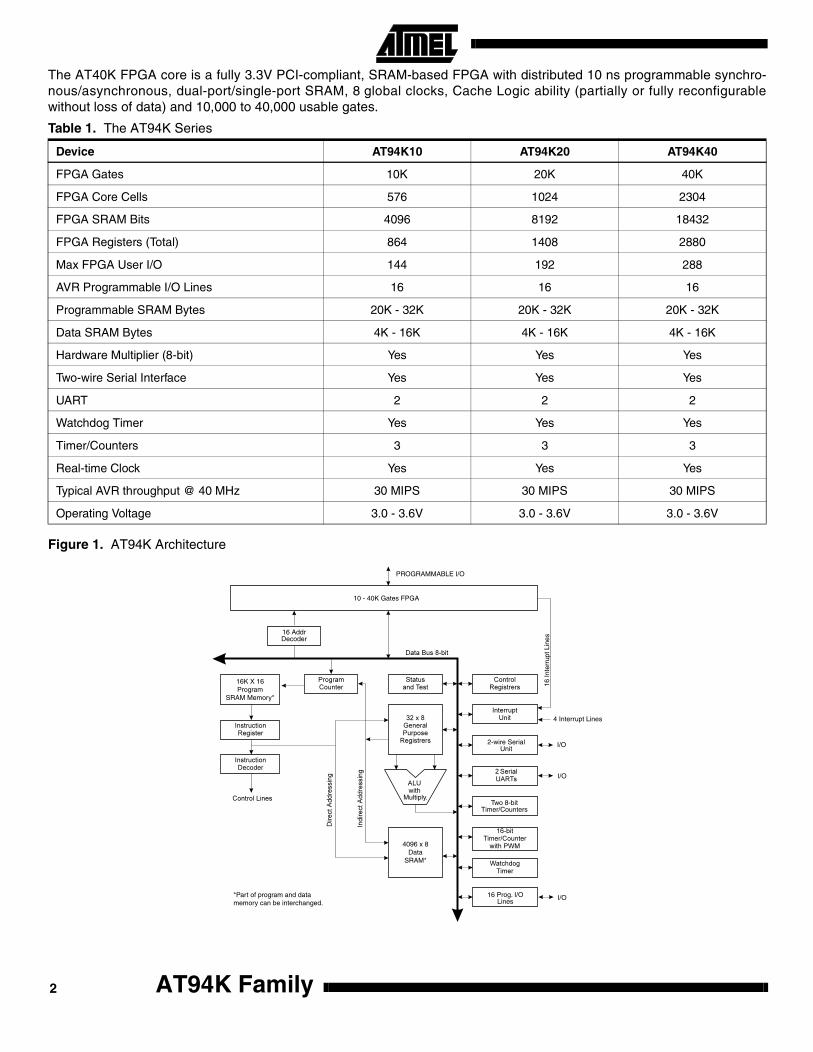
The Busing NetworkFigure 3 depicts one of five identical FPGA busing planes. Each plane has three bus resources: a local-bus resource (themiddle bus) and two express-bus resources. Bus resources are connected via repeaters. Each repeater has connections totwo adjacent local-bus segments and two express-bus segments. Each local-bus segment spans four cells and connects toconsecutive repeaters. Each express-bus segment spans eight cells and “leapfrogs” or bypasses a repeater. Repeatersregenerate signals and can connect any bus to any other bus (all pathways are legal) on the same plane. Although notshown, a local bus can bypass a repeater via a programmable pass gate allowing long on-chip tri-state buses to becreated. Local/local turns are implemented through pass gates in the cell-bus interface (see following page).Express/Express turns are implemented through separate pass gates distributed throughout the array.
Figure 3. Busing Plane (one of five)
= Local/Local or Express/Express Turn Point
= AT40K Core Cell
= Row Repeater
= Column
AT94K Family6
AT94K Family
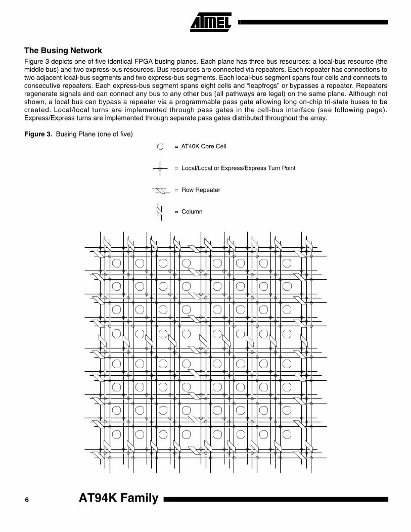
Cell ConnectionsFigure 4(a) depicts direct connections between an FPGA cell and its eight nearest neighbors. Figure 4(b) shows theconnections between a cell five horizontal local buses (one per busing plane) and five vertical local buses (one per busingplane).
Figure 4. Cell Connections
CEL CEL
CEL CEL CEL
CEL CEL
CEL
CEL
CEL
(a) Cell-to-Cell Connections (b) Cell-to-Bus Connections
WXYZL
WXYZLYX
Y
Y
Y
X
X X
7
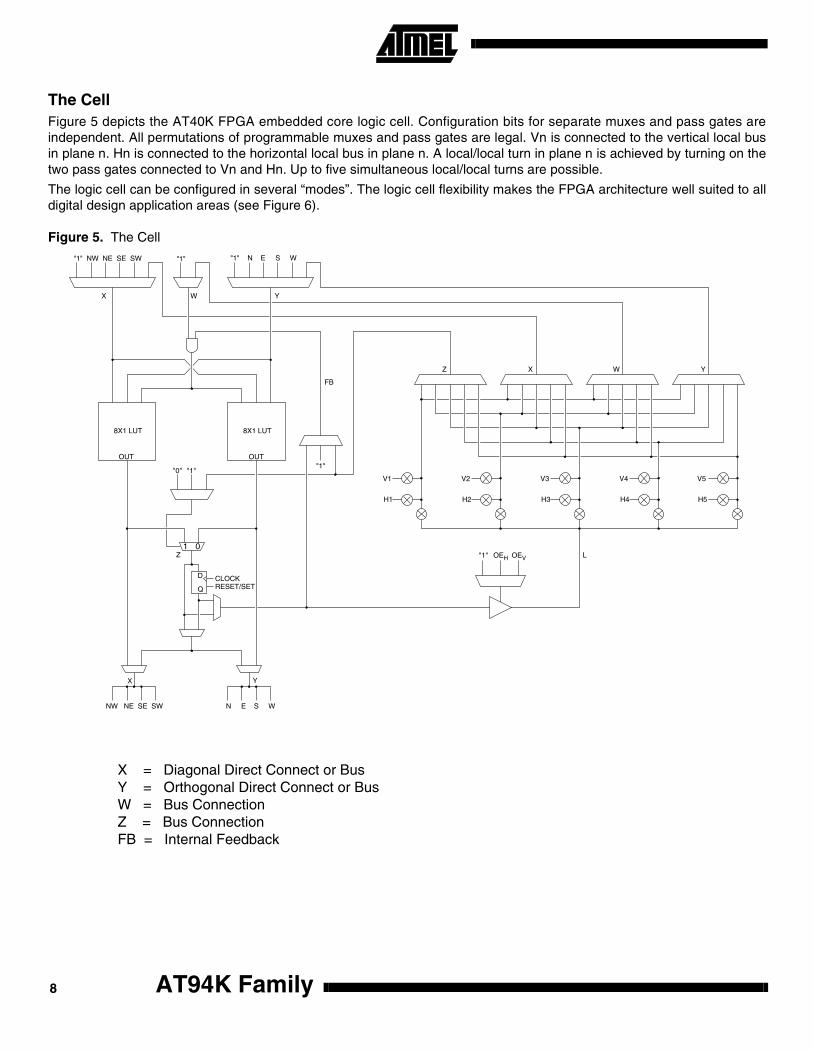
The CellFigure 5 depicts the AT40K FPGA embedded core logic cell. Configuration bits for separate muxes and pass gates areindependent. All permutations of programmable muxes and pass gates are legal. Vn is connected to the vertical local busin plane n. Hn is connected to the horizontal local bus in plane n. A local/local turn in plane n is achieved by turning on thetwo pass gates connected to Vn and Hn. Up to five simultaneous local/local turns are possible.
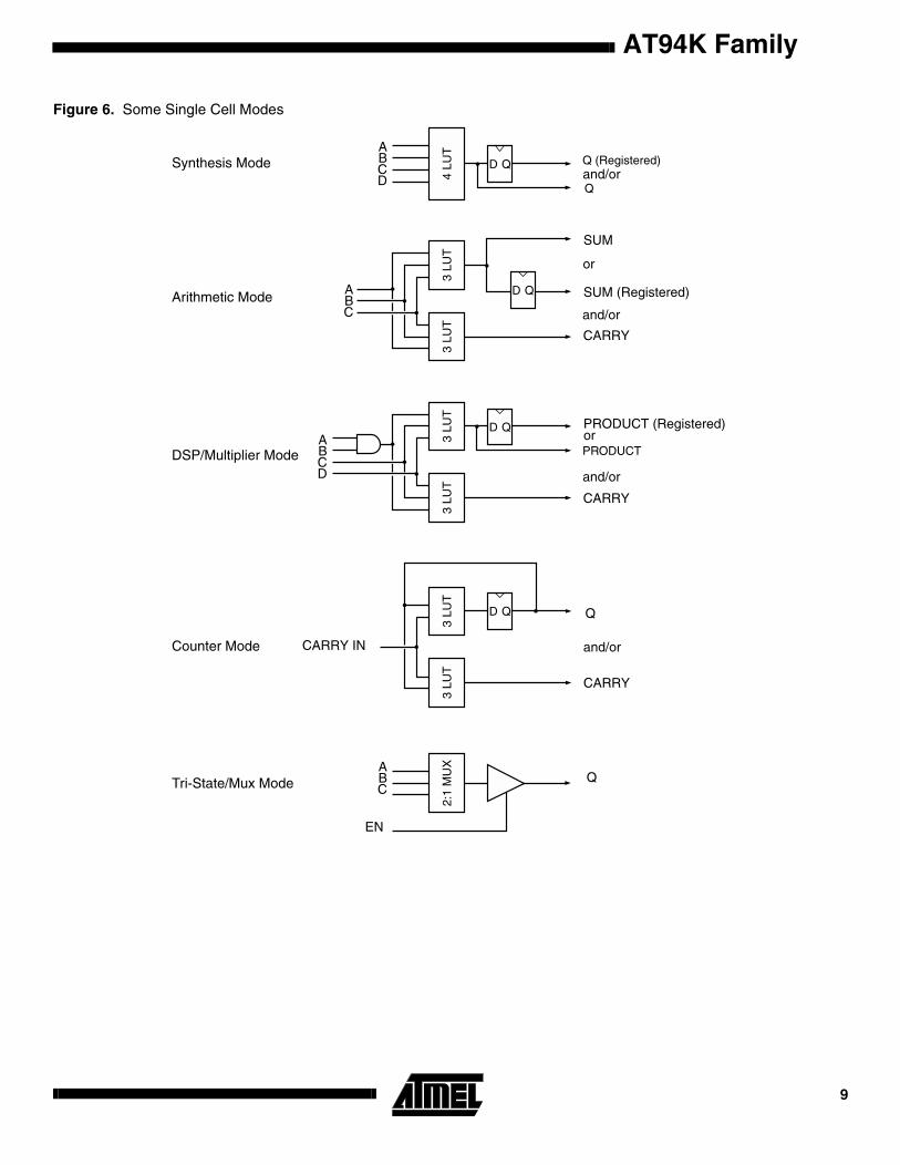
The logic cell can be configured in several “modes”. The logic cell flexibility makes the FPGA architecture well suited to alldigital design application areas (see Figure 6).
Figure 5. The Cell
OUT OUT
RESET/SETCLOCK
FB
X = Diagonal Direct Connect or BusY = Orthogonal Direct Connect or BusW = Bus ConnectionZ = Bus ConnectionFB = Internal Feedback
1 0Z
D
Q
"1" NW NE SE SW "1"
"1""1""0"
X W Y
XZ W Y
"1" N E S W
8X1 LUT 8X1 LUT
X Y
NW NE SE SW N E S W
V1
H1
V2
H2
V3
H3
V4
H4
V5
H5
"1" OEH OEV L
AT94K Family8
AT94K Family
Figure 6. Some Single Cell Modes
3 LU
T3
LUT
3 LU
T3
LUT
4 LU
T2:
1M
UX
3 LU
T3
LUT
D Q
D Q
Q
Q (Registered)
D Q
D Q
Synthesis Mode
Arithmetic Mode
DSP/Multiplier Mode
Counter Mode
Tri-State/Mux Mode
ABCD
ABC
ABCD
ABC
EN
Q
Q
SUM (Registered)
SUM
and/or
PRODUCTor
CARRY
PRODUCT (Registered)
CARRY
CARRY
CARRY IN
and/or
or
and/or
and/or
9
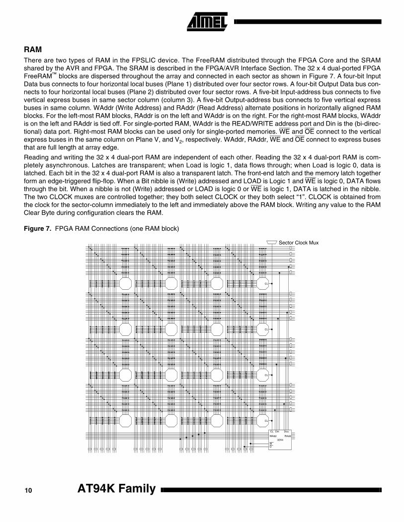
RAMThere are two types of RAM in the FPSLIC device. The FreeRAM distributed through the FPGA Core and the SRAMshared by the AVR and FPGA. The SRAM is described in the FPGA/AVR Interface Section. The 32 x 4 dual-ported FPGAFreeRAM™ blocks are dispersed throughout the array and connected in each sector as shown in Figure 7. A four-bit InputData bus connects to four horizontal local buses (Plane 1) distributed over four sector rows. A four-bit Output Data bus con-nects to four horizontal local buses (Plane 2) distributed over four sector rows. A five-bit Input-address bus connects to fivevertical express buses in same sector column (column 3). A five-bit Output-address bus connects to five vertical expressbuses in same column. WAddr (Write Address) and RAddr (Read Address) alternate positions in horizontally aligned RAMblocks. For the left-most RAM blocks, RAddr is on the left and WAddr is on the right. For the right-most RAM blocks, WAddris on the left and RAddr is tied off. For single-ported RAM, WAddr is the READ/WRITE address port and Din is the (bi-direc-tional) data port. Right-most RAM blocks can be used only for single-ported memories. WE and OE connect to the verticalexpress buses in the same column on Plane V, and V2, respectively. WAddr, RAddr, WE and OE connect to express busesthat are full length at array edge.
Reading and writing the 32 x 4 dual-port RAM are independent of each other. Reading the 32 x 4 dual-port RAM is com-pletely asynchronous. Latches are transparent; when Load is logic 1, data flows through; when Load is logic 0, data islatched. Each bit in the 32 x 4 dual-port RAM is also a transparent latch. The front-end latch and the memory latch togetherform an edge-triggered flip-flop. When a Bit nibble is (Write) addressed and LOAD is Logic 1 and WE is logic 0, DATA flowsthrough the bit. When a nibble is not (Write) addressed or LOAD is logic 0 or WE is logic 1, DATA is latched in the nibble.The two CLOCK muxes are controlled together; they both select CLOCK or they both select “1”. CLOCK is obtained fromthe clock for the sector-column immediately to the left and immediately above the RAM block. Writing any value to the RAMClear Byte during configuration clears the RAM.
Figure 7. FPGA RAM Connections (one RAM block)
32X4
Din
WAdd
WO
Dou
RAdd
CL
CL
CL
CL
CL
Sector Clock Mux
AT94K Family10

AT94K Family
Figure 8. FreeRAM Logic
Write
Data Data
Read
"1""1"
Write Enable
RAM-Clear
DATA OUT
"1"
CLOCK
Load5
READ ADDR
WRITE ADDR
WE
DATA IN
LoadLatch
LoadLatch
LoadLatch
Clear
32 x 4DUAL-PORT
RAMOE
44
5
11
12
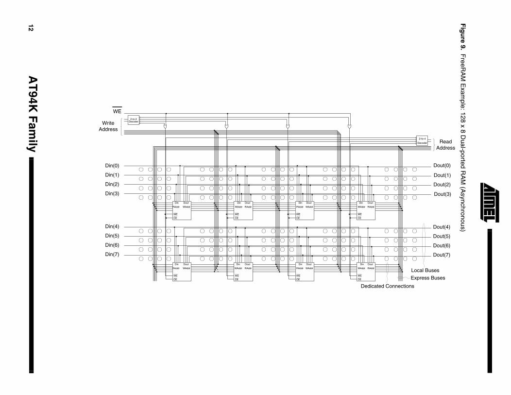
Fig
ure 9. F
reeRA
M E
xample: 128 x 8 D
ual-ported RA
M (A
synchronous)Dout(4)
Dout(5)
Dout(6)
Dout(7)
2-to-4
Decoder
Local Buses
Express Buses
ed Connections
ReadAddress
Dout(0)
Dout(1)
Dout(2)
Dout(3)
AT
94K F
amily
2-to-4 Decoder
Din Dout
WE
OE
RAddr WAddr
Din Dout Din Dout
WE
OE
Din Dout
WAddr RAddr
WE
OE
RAddr WAddr
WE
OE
WAddr RAddr
Din Dout
WAddr RAddr
WE
OE
Din Dout
WE
OE
RAddr WAddr
Din Dout
WAddr RAddr
WE
OE
Din Dout
WE
OE
RAddr WAddr
Dedicat
Din(0)
Din(1)
Din(2)
Din(3)
Din(4)
Din(5)
Din(6)
Din(7)
WriteAddress
WE
AT94K Family
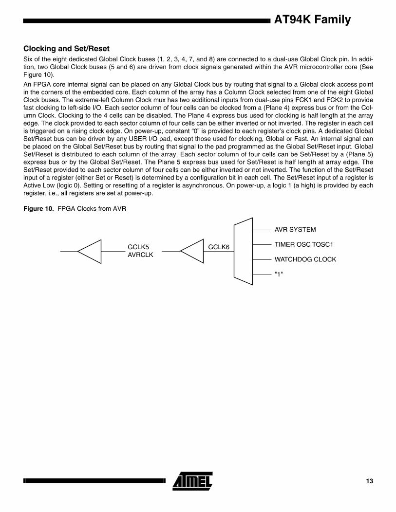
Clocking and Set/ResetSix of the eight dedicated Global Clock buses (1, 2, 3, 4, 7, and 8) are connected to a dual-use Global Clock pin. In addi-tion, two Global Clock buses (5 and 6) are driven from clock signals generated within the AVR microcontroller core (SeeFigure 10).
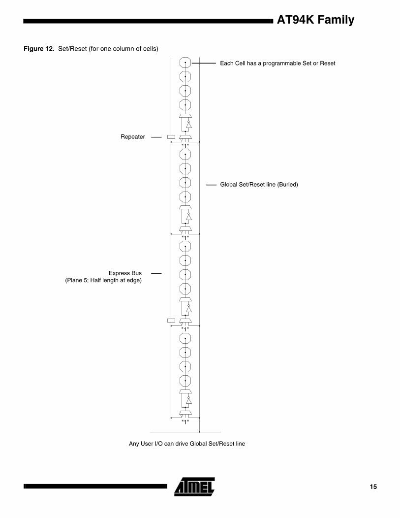
An FPGA core internal signal can be placed on any Global Clock bus by routing that signal to a Global clock access pointin the corners of the embedded core. Each column of the array has a Column Clock selected from one of the eight GlobalClock buses. The extreme-left Column Clock mux has two additional inputs from dual-use pins FCK1 and FCK2 to providefast clocking to left-side I/O. Each sector column of four cells can be clocked from a (Plane 4) express bus or from the Col-umn Clock. Clocking to the 4 cells can be disabled. The Plane 4 express bus used for clocking is half length at the arrayedge. The clock provided to each sector column of four cells can be either inverted or not inverted. The register in each cellis triggered on a rising clock edge. On power-up, constant “0” is provided to each register’s clock pins. A dedicated GlobalSet/Reset bus can be driven by any USER I/O pad, except those used for clocking, Global or Fast. An internal signal canbe placed on the Global Set/Reset bus by routing that signal to the pad programmed as the Global Set/Reset input. GlobalSet/Reset is distributed to each column of the array. Each sector column of four cells can be Set/Reset by a (Plane 5)express bus or by the Global Set/Reset. The Plane 5 express bus used for Set/Reset is half length at array edge. TheSet/Reset provided to each sector column of four cells can be either inverted or not inverted. The function of the Set/Resetinput of a register (either Set or Reset) is determined by a configuration bit in each cell. The Set/Reset input of a register isActive Low (logic 0). Setting or resetting of a register is asynchronous. On power-up, a logic 1 (a high) is provided by eachregister, i.e., all registers are set at power-up.
Figure 10. FPGA Clocks from AVR
AVR SYSTEM
TIMER OSC TOSC1GCLK5AVRCLK
WATCHDOG CLOCK
"1"
GCLK6
13
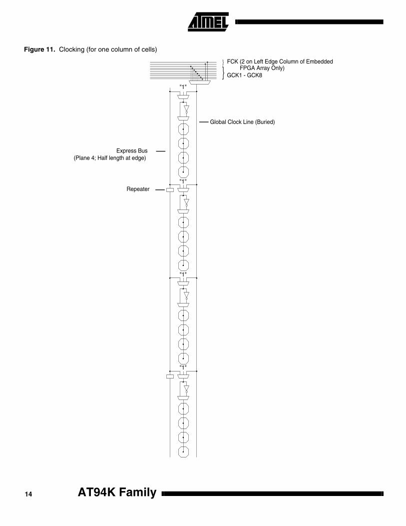
Figure 11. Clocking (for one column of cells)
Global Clock Line (Buried)
Express Bus(Plane 4; Half length at edge)
GCK1 - GCK8
Repeater
}}
"1"
"1"
"1"
"1"
FCK (2 on Left Edge Column of EmbeddedFPGA Array Only)
AT94K Family14
AT94K Family
Figure 12. Set/Reset (for one column of cells)
Each Cell has a programmable Set or Reset
Global Set/Reset line (Buried)
Repeater
Express Bus(Plane 5; Half length at edge)
Any User I/O can drive Global Set/Reset line
"1"
"1"
"1"
"1"
15
Some of the bus resource on the embedded FPGA core are used as dual-function resource. Table 2 shows which busesare used in a dual-function mode and which bus plane is used. The FPGA software tools are designed to accommodatedual-function buses in an efficient manner.
Table 2. Dual-function Buses
Function Type Plane(s) Direction Comments
Cell Output Enable Local 5 Horizontal and Vertical
FreeRAM Output Enable Express 2 Vertical Bus full length at array edgeBus in first column to left of RAM block
FreeRAM Write Enable Express 1 Vertical Bus full length at array edgeBus in first column to left of RAM block
FreeRAM Address Express 1 - 5 Vertical Buses full length at array edgeBuses in second column to left of RAM block
FreeRAM Data In Local 1 Horizontal
FreeRAM Data Out Local 2 Horizontal
Clocking Express 4 Vertical Bus half length at array edge
Set/Reset Express 5 Vertical Bus half length at array edge
AT94K Family16

AT94K Family
Section 2 – FPGA/AVR Interface and System ControlThe FPGA and AVR share a flexible interface which allows for many methods of system integration. • Both FPGA and AVR share access to the 15 ns dual-port SRAM.
• The AVR data bus interfaces directly into the FPGA busing resources, effectively treating the FPGA as a large I/O device. Users have complete flexibility on the types of additional peripherals which are placed and routed inside the FPGA user logic. 16 decoded address lines are provided into the FPGA.
• 16 interrupts are available from the FPGA to the AVR MCU.
• The AVR can reprogram the FPGA Cache Logic during operation to create a dynamic reconfigurable system.
FPGA/AVR Interface – Memory-mapped PeripheralsThe FPGA core can be directly accessed by the AVR core (as shown in Figure 13). Four memory locations in the AVRmemory map are decoded into 16 select lines and are presented to the FPGA along with the AVR 8-bit data bus. TheFPGA can be used to create additional custom peripherals for the AVR microcontroller through this interface. In additionthere are 16 interrupt lines from the FPGA back into the AVR interrupt controller. Programmable peripherals or regular logiccan use these interrupt lines. Full support for programmable peripherals is available within the System Designer tool suite.
Figure 13. FPGA/AVR Interface: Interrupts and Addressing
The FPGA I/O selection is controlled by the AVR. This is described in detail beginning on page 44. The FPGA I/O interruptsare described beginning on page 45.
EMBEDDEDFPGA CORE
EMBEDDEDAVR CORE
ADDRESSDECODER
4:16DECODE
16 Memory-mappedDecoded AddressLines from 4 I/O Memory Space Addresses I/O Memory Address Bus
FPGAIORE
FPGAIOWE
16 Interrupt Lines from FPGA to AVR – Various Priority Levels
8-bit Bidirectional Data Bus
8-bitData Out
8-bitData In
17

Program and Data SRAMBetween the FPGA and the AVR resides 36K of 15 ns dual -port SRAM. This SRAM is used primarily by the AVR for pro-gram instruction and general-purpose data storage. The AVR is connected to one side of this SRAM; the FPGA isconnected to the other side. The port connected to the FPGA is used during configuration download to load the AVR pro-gram and data memory. It is also used by the FPGA to store data without using up bandwidth on the AVR system data bus.
The FPGA core, except in its optional support for AVR peripherals, does not interact directly with the AVR core. The FPGAcore communicates directly with the data SRAM block, viewing all SRAM memory space as 8-bit memory.
The internal program and data SRAM is divided into three blocks: 10K x 16 dedicated program SRAM, 4K x 8 dedicateddata SRAM, and 6K x 16 or 12K x 8 configurable SRAM which may be swapped between program and data memoryspaces in 2K x 16 or 4K x 8 partitions.
The addressing scheme for the configurable SRAM partitions prevents program instructions from overwriting data wordsand vice versa. Once configured (SCR40:41 – see System Control Register on page 23), the program memory spaceremains isolated from the data memory space. SCR40:41 control internal muxes and write enable signals allow the mem-ory to be safely segmented.
Figure 14. FPSLIC Configurable Allocation SRAM Memory
$0000
$27FF
$3FFF
$3800
$3000
$37FF
$2800
$2FFF
$0FFF
$1000
$1FFF$2000
$2FFF
$3000
$3FFF
$005F
Memory Partitionis User Defined
during Development FIXED10K x 16
OPTIONAL2K x 16
OPTIONAL2K x 16
OPTIONAL2K x 16
OPTIONAL4K x 8
OPTIONAL4K x 8
OPTIONAL4K x 8
Program SRAM Memory
Data SRAM Memory
FIXED4K x 8
$0000
Reserved FPGA Access Only
$001F
AVR Reg. Space
AT94K Family18

AT94K Family
Data SRAM Access by FPGA – FPGAFrame™ ModeThe FPGA user logic has access to the AVR data SRAM directly through the FPGA side of the dual-port memory. A singlebit in the configuration control register (SCR63 – see System Control Register on page 24) enables this interface. The inter-face is disabled during configuration downloads. Express buses on the East edge of the array are used to interface thememory. Full read and write access is available. The interface itself is dedicated in routing resources, and is available in theSystem Designer software suite as a macro.
Figure 15. Internal SRAM Access
There is no read enable from the FPGA side. This means that the read is always enabled. You can read and write to thesame location at one time on the FPGA side. You can also perform a read or write from the AVR at the same time as anFPGA read or write. If there is a possibility of an address being accessed by both devices, at the same time, the designershould add some arbitration to control who has priority. In most cases the AVR will be used to restrict access by the FPGAusing SCR63 – see System Control Register on page 24.
AVR Cache ModeThe AVR has the ability to cache download the FPGA memory. The AVR has direct access to the data buses of the config-uration SRAM and is able to download bitstreams. AVR Cache access of configuration SRAM is not available duringnormal configuration downloads. If attempted, an interrupt back to the AVR will be generated. The Cache Logic port in theAVR is located in the I/O memory map. Three registers, FPGAX, FPGAY FPGAZ, control the address written to inside theFPGA; and FPGAD in the AVR memory map controls the Data. Registers FPGAX, FPGAY and FPGAZ are write only.
The AVR Cache Logic access mode is write only. Transfers may be aborted at any time due to AVR program wishes orexternal interrupts.
The FPGA CHECK mode is not supported by the AVR Cache mode.
A typical application for this mode is for the AVR to accept serial data through a UART and port it as configuration data tothe FPGA, thereby affecting a download, or allowing reconfigurable systems where the FPGA is updated algorithmically byAVR. Please refer to FPSLIC Configuration datasheet for more details.
See page 43 “FPGA Cache Logic” for more details.
EMBEDDEDFPGA CORE
EMBEDDEDAVR CORE
DATA SRAM4K x 8UP TO 16K x 8
16 Address Lines: FPGA Edge Express Buses 16-bit Data Address Bus
CLK AVR
WE AVR
RE AVR
8-bit Data Write
8-bit Data Read/Write
CLK FPGA
WE FPGA
8-bit Data Read
19
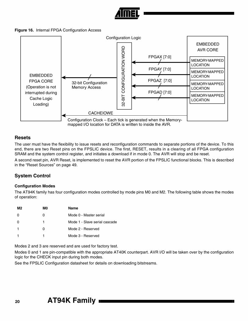
Figure 16. Internal FPGA Configuration Access
ResetsThe user must have the flexibility to issue resets and reconfiguration commands to separate portions of the device. To thisend, there are two Reset pins on the FPSLIC device. The first, RESET, results in a clearing of all FPGA configurationSRAM and the system control register, and initiates a download if in mode 0. The AVR will stop and be reset.
A second reset pin, AVR Reset, is implemented to reset the AVR portion of the FPSLIC functional blocks. This is describedin the “Reset Sources” on page 49.
System Control
Configuration Modes
The AT94K family has four configuration modes controlled by mode pins M0 and M2. The following table shows the modesof operation:
Modes 2 and 3 are reserved and are used for factory test.
Modes 0 and 1 are pin-compatible with the appropriate AT40K counterpart. AVR I/O will be taken over by the configurationlogic for the CHECK input pin during both modes.
See the FPSLIC Configuration datasheet for details on downloading bitstreams.
M2 M0 Name
0 0 Mode 0 - Master serial
0 1 Mode 1 - Slave serial cascade
1 0 Mode 2 - Reserved
1 1 Mode 3 - Reserved
EMBEDDEDFPGA CORE
(Operation is notinterrupted during
Cache LogicLoading)
EMBEDDEDAVR CORE
32-B
IT C
ON
FIG
UR
ATIO
N W
OR
D
Configuration Logic
FPGAD [7:0]
32-bit Configuration Memory Access
FPGAX [7:0]
FPGAY [7:0]
FPGAZ [7:0]
Configuration Clock – Each tick is generated when the Memory-mapped I/O location for DATA is written to inside the AVR.
MEMORY-MAPPEDLOCATION
MEMORY-MAPPEDLOCATION
MEMORY-MAPPEDLOCATION
MEMORY-MAPPEDLOCATION
CACHEIOWE
AT94K Family20
AT94K Family
System Control Register – FPGA/AVR
The configuration control register in the FPSLIC consists of 8 bytes of data, which are loaded at power-up from externalnonvolatile memory. FPSLIC System Control Register defaults are set in the system designer software.
SCR2 controls the operation of the dual-function I/O CSOUT. When SCR2 is set, the CSOUT pin is not used by the config-uration during downloads.
SCR3 controls the operation of the CHECK pin and enables the Check Function. When SCR3 is set, the CHECK pin is notused by the configuration during downloads.
SCR4 is the Security Flag and controls the writing and checking of configuration memory during any subsequent configura-tion download. When SCR4 is set, any subsequent configuration download initiated by the user, whether a normaldownload or a CHECK function download, causes the INIT pin to immediately activate. CON is released, and no furtherconfiguration activity takes place. The download sequence during which SCR4 is set is NOT affected. The Control Registerwrite is also prohibited, so bit SCR4 may only be cleared by a power-on reset or manual reset.
Setting SCR6 makes the OTS pin an input which controls the global tri-state control for all user I/O.
SCR0 : Reserved
SCR1 : Reserved
SCR2 : 0 = Enable cascading
1 = Disable cascading
SCR3 : 0 = Check function enabled
1 = Check function disabled
SCR4 : 0 = Memory lockout disabled
1 = Memory lockout enabled
SCR5 : Reserved
SCR6 : 0 = OTS disabled
1 = OTS enabled
SCR7 : Reserved
SCR8 : Reserved
SCR9 : Reserved
SCR10 : Reserved
SCR11 : Reserved
SCR12 : Reserved
SCR13 : 0 = CCLK normal operation
1 = CCLK continues after configuration
21
Setting bit SCR13 allows the CCLK pin to continue to run after configuration download is completed. This bit is valid forMaster mode.
Bits SCR14 and SCR15 speed up the internal oscillator and allow the Master mode to drive CCLK at 1, 2, 4 or 8 MHz.Setting these bits immediately enables the higher CCLK frequency used in mode 0 configuration.
Setting SCR16:SCR23 allows the user to disable the input buffers driving the global clocks. The clock buffers are enabledand disabled synchronously with the rising edge of the respective GCLK signal, and stop in a high “1” state. Setting one ofthese bits disables the appropriate GCLK input buffer only and has no effect on the connection from the input buffer to theFPGA array.
Setting SCR24:SCR25 allows the user to disable the input buffers driving the fast clocks. The clock buffers are enabledand disabled synchronously with the rising edge of the respective FCLK signal, and stop in a high “1” state. Setting one ofthese bits disables the appropriate FCLK input buffer only and has no effect on the connection from the input buffer to theFPGA array.
SCR30 allows the Global set/reset hold the core DFFs in reset during any configuration download. The Global set/reset netis released at the end of configuration download on the rising edge of CON.
SCR31 forces all user defined I/O pins to go tri-state during configuration download. Tri-state is released at the end ofconfiguration download on the rising edge of CON.
SCR14 : SCR15 : 00 = 1 MHz
01 = 2 MHz
10 = 4 MHz
11 = 8 MHz
SCR16 : SCR23 : 0 = GCLK 0:7 always enabled
1 = GCLK 0:7 disabled during configuration download
SCR24 : SCR25 : 0 = FCLK 0:1 always enabled
1 = FCLK 0:1 disabled during configuration download.
SCR26 : Reserved
SCR27 : Reserved
SCR28 : Reserved
SCR29 : Reserved
SCR30 : 0 = Global set/reset normal
1 = Global set/reset active (low) during configuration
SCR31 : 0 = Disable I/O tri-state
1 = I/O tri-state during configuration
SCR32 : Reserved
AT94K Family22

AT94K Family
SCR36 protects AVR program code from writes by the FPGA Data SRAM writes.
SCR40 : SCR41 AVR program/data SRAM partitioning (Set by System Designer):
SCR48 : SCR53 Defaults dependent on package selected.
On packages less than 144-pins, there is reduced access to AVR ports. Port D is not available externally in the smallestpackage and Port E becomes dual-purpose I/O to maintain access to the UARTs and external interrupt pins. The Pin List(East Side), page 120 shows exactly which pins are available in each package.
SCR33 : Reserved
SCR34 : Reserved
SCR35 : 0 = AVR reset pin disabled
1 = AVR reset pin enabled
SCR36 : 0 = Protect AVR program SRAM (Excluding Boot Block)
1 = Allow writes to AVR program SRAM (Excluding Boot Block)
SCR37 : 0 = AVR program SRAM Boot Block protect
1 = AVR program SRAM Boot Block allows over write
SCR38 : Reserved
SCR39 : Reserved
SCR40 : SCR41 00 = 16K Program/4K Data
01 = 14K Program/8K Data
10 = 12K Program/12K Data
11 = 10K Program/16K Data
SCR42 : SCR46 Reserved
SCR47 : Reserved
SCR48 : 0 = EXT-INT0 driven by Port E<4>
1 = EXT-INT0 driven by INTP0 pad
SCR49 : 0 = EXT-INT1 driven by Port E<5>
1 = EXT-INT1 driven by INTP1 pad
SCR50 : 0 = EXT-INT2 driven by Port E<6>
1 = EXT-INT2 driven by INTP2 pad
23
SCR51 : 0 = EXT-INT3 driven by Port E<7>
1 = EXT-INT3 driven by INTP3 pad
SCR52 : 0 = UART0 pins assigned to Port E<1:0>
1 = UART0 pins assigned to UART0 pads
SCR53 : 0 = UART1 pins assigned to Port E<3:2>
1 = UART1 pins assigned to UART1 pads
SCR54 : 0 = AVR port D I/O with 6 mA drive
1 = AVR port D I/O with 24 mA drive
SCR55 : 0 = AVR port E I/O with 6 mA drive
1 = AVR port E I/O with 24 mA drive
SCR56 : Reserved
SCR57 : Reserved
SCR58 : XTAL2 pad I/O buffer disable
SCR59 : Reserved
SCR60 : SCR61 Global Clock 6 mux select:
00 = “1”
01 = AVR system clock
10 = Timer oscillator clock (TOSC)
11 = Watchdog clock
SCR62 : 0 = disable cache writes to FPGA by AVR
1 = enable cache writes to FPGA by AVR
SCR63 : 0 = disable writes to SRAM by FPGA
1 = enable writes to SRAM by FPGA
AT94K Family24
AT94K Family
Section 3 – AVR Core and Peripherals• AVR Core
• Watchdog Timer/On-chip Oscillator
• Oscillator-to-Internal Clock Circuit
• Oscillator -to-Timer/Counter for Real-time Clock
• 16-bit Timer/Counter and Two 8-bit Timer/Counters
• Interrupt Unit
• UART (0)
• UART (1)
• I/O Port D (full 8 bits available on 144 pin or higher devices)
• I/O Port E
The embedded AVR core is a low-power CMOS 8-bit microcontroller based on the AVR RISC architecture. By executingpowerful instructions in a single-clock-cycle, the embedded AVR core achieves throughputs approaching 1 MIPS per MHzallowing the system architect to optimize power consumption versus processing speed.
The AVR core is based on an enhanced RISC architecture that combines a rich instruction set with 32 x 8 general-purpose working registers. All the 32 x 8 registers are directly connected to the Arithmetic Logic Unit (ALU), allowing twoindependent register bytes to be accessed in one single instruction executed in 1-clock-cycle. The resulting architecture ismore code efficient while achieving throughputs up to ten times faster than conventional CISC microcontrollers.
The embedded AVR core provides the following features: 4K bytes SRAM, 16 general-purpose I/O lines, 32 x 8 general-purpose working registers, Real-time Counter (RTC), 3 flexible timer/counters with compare modes and PWM, 2 UARTs,programmable Watchdog Timer with internal oscillator, 2-wire serial port and three software-selectable Power-savingmodes. The Idle mode stops the CPU while allowing the SRAM, timer/counters, two-wire serial port and interrupt system tocontinue functioning. The Power-down mode saves the register contents but freezes the oscillator, disabling all other chipfunctions until the next interrupt or hardware reset. In Power-save mode, the timer oscillator continues to run, allowing theuser to maintain a timer base while the rest of the device is sleeping.
The embedded AVR core is supported with a full suite of program and system development tools including: C compilers,macro assemblers, program debugger/simulators and evaluation kits.
Instruction Set Nomenclature (Summary)Full instruction details available in the AVR Instruction Set document.
Status Register (SREG)
SREG: Status register
C: Carry flag in status register
Z: Zero flag in status register
N: Negative flag in status register
V: Two’s complement overflow indicator
S: N ⊕ V, For signed tests
H: Half-carry flag in the status register
T: Transfer bit used by BLD and BST instructions
I: Global interrupt enable/disable flag
25
Registers and Operands
Rd: Destination (and source) register in the register file
Rr: Source register in the register file
R: Result after instruction is executed
K: Constant data
k: Constant address
b: Bit in the register file or I/O register (0 ≤ b ≤ 7)
s: Bit in the status register (0 ≤ s ≤ 2)
X,Y,Z: Indirect address register (X=R27:R26, Y=R29:R28 and Z=R31:R30)
A: I/O location address
q: Displacement for direct addressing (0 ≤ q ≤ 63)
I/O Registers
Stack
STACK: Stack for return address and pushed registers
SP: Stack Pointer to STACK
Flags
⇔: Flag affected by instruction
0: Flag cleared by instruction
1: Flag set by instruction
-: Flag not affected by instruction
The instructions EIJMP, EICALL, ELPM, GPM, ESPM (from megaAVR™ Instruction Set) are not supported in the FPSLICdevice.
Conditional Branch Summary
Test Boolean Mnemonic Complementary Boolean Mnemonic Comment
Rd > Rr Z•(N ⊕ V) = 0 BRLT Rd ≤ Rr Z+(N ⊕ V) = 1 BRGE Signed
Rd ≥ Rr (N ⊕ V) = 0 BRGE Rd < Rr (N ⊕ V) = 1 BRLT Signed
Rd = Rr Z = 1 BREQ Rd ≠ Rr Z = 0 BRNE Signed
Rd ≤ Rr Z+(N ⊕ V) = 1 BRGE Rd > Rr Z•(N ⊕ V) = 0 BRLT Signed
Rd < Rr (N ⊕ V) = 1 BRLT Rd ≥ Rr (N ⊕ V) = 0 BRGE Signed
Rd > Rr C + Z = 0 BRLO Rd ≤ Rr C + Z = 1 BRSH Unsigned
Rd ≥ Rr C = 0 BRSH/BRCC Rd < Rr C = 1 BRLO/BRCS Unsigned
Rd = Rr Z = 1 BREQ Rd ≠ Rr Z = 0 BRNE Unsigned
Rd ≤ Rr C + Z = 1 BRSH Rd > Rr C + Z = 0 BRLO Unsigned
Rd < Rr C = 1 BRLO/BRCS Rd ≥ Rr C = 0 BRSH/BRCC Unsigned
Carry C = 1 BRCS No carry C = 0 BRCC Simple
Negative N = 1 BRMI Positive N = 0 BRPL Simple
Overflow V = 1 BRVS No overflow V = 0 BRVC Simple
Zero Z = 1 BREQ Not zero Z = 0 BRNE Simple
AT94K Family26
AT94K Family
Complete Instruction Set Summary
Instruction Set Summary
Mnemonics Operands Description Operation Flags#Clock Note
Arithmetic and Logic Instructions
ADD Rd, Rr Add without Carry Rd ← Rd + Rr Z,C,N,V,S,H 1
ADC Rd, Rr Add with Carry Rd ← Rd + Rr + C Z,C,N,V,S,H 1
ADIW Rd, K Add Immediate to Word Rd+1:Rd ← Rd+1:Rd + K Z,C,N,V,S 2
SUB Rd, Rr Subtract without Carry Rd ← Rd - Rr Z,C,N,V,S,H 1
SUBI Rd, K Subtract Immediate Rd ← Rd - K Z,C,N,V,S,H 1
SBC Rd, Rr Subtract with Carry Rd ← Rd - Rr - C Z,C,N,V,S,H 1
SBCI Rd, K Subtract Immediate with Carry Rd ← Rd - K - C Z,C,N,V,S,H 1
SBIW Rd, K Subtract Immediate from Word Rd+1:Rd ← Rd+1:Rd - K Z,C,N,V,S 2
AND Rd, Rr Logical AND Rd ← Rd • Rr Z,N,V,S 1
ANDI Rd, K Logical AND with Immediate Rd ← Rd • K Z,N,V,S 1
OR Rd, Rr Logical OR Rd ← Rd v Rr Z,N,V,S 1
ORI Rd, K Logical OR with Immediate Rd ← Rd v K Z,N,V,S 1
EOR Rd, Rr Exclusive OR Rd ← Rd ⊕ Rr Z,N,V,S 1
COM Rd One’s Complement Rd ← $FF - Rd Z,C,N,V,S 1
NEG Rd Two’s Complement Rd ← $00 - Rd Z,C,N,V,S,H 1
SBR Rd, K Set Bit(s) in Register Rd ← Rd v K Z,N,V,S 1
CBR Rd, K Clear Bit(s) in Register Rd ← Rd • ($FFh - K) Z,N,V,S 1
INC Rd Increment Rd ← Rd + 1 Z,N,V,S 1
DEC Rd Decrement Rd ← Rd - 1 Z,N,V,S 1
TST Rd Test for Zero or Minus Rd ← Rd • Rd Z,N,V,S 1
CLR Rd Clear Register Rd ← Rd ⊕ Rd Z,N,V,S 1
SER Rd Set Register Rd ← $FF None 1
MUL Rd, Rr Multiply Unsigned R1:R0 ← Rd × Rr (UU) Z,C 2
MULS Rd, Rr Multiply Signed R1:R0 ← Rd × Rr (SS) Z,C 2
MULSU Rd, Rr Multiply Signed with Unsigned R1:R0 ← Rd × Rr (SU) Z,C 2
FMUL Rd, Rr Fractional Multiply Unsigned R1:R0 ← (Rd × Rr)<<1 (UU) Z,C 2
FMULS Rd, Rr Fractional Multiply Signed R1:R0 ← (Rd × Rr)<<1 (SS) Z,C 2
FMULSU Rd, Rr Fractional Multiply Signed with Unsigned
R1:R0 ← (Rd × Rr)<<1 (SU) Z,C 2
Branch Instructions
RJMP k Relative Jump PC ← PC + k + 1 None 2
IJMP Indirect Jump to (Z) PC(15:0) ← Z None 2
JMP k Jump PC ← k None 3
27

RCALL k Relative Call Subroutine PC ← PC + k + 1 None 3
ICALL Indirect Call to (Z) PC(15:0) ← Z None 3
CALL k Call Subroutine PC ← k None 4
RET Subroutine Return PC ← STACK None 4
RETI Interrupt Return PC ← STACK I 4
CPSE Rd, Rr Compare, Skip if Equal if (Rd = Rr) PC ← PC + 2 or 3 None 1 / 2 / 3
CP Rd, Rr Compare Rd - Rr Z,C,N,V,S,H 1
CPC Rd, Rr Compare with Carry Rd - Rr - C Z,C,N,V,S,H 1
CPI Rd, K Compare with Immediate Rd - K Z,C,N,V,S,H 1
SBRC Rr, b Skip if Bit in Register Cleared if (Rr(b)=0) PC ← PC + 2 or 3 None 1 / 2 / 3
SBRS Rr, b Skip if Bit in Register Set if (Rr(b)=1) PC ← PC + 2 or 3 None 1 / 2 / 3
SBIC A, b Skip if Bit in I/O Register Cleared if(I/O(A,b)=0) PC ← PC + 2 or 3 None 1 / 2 / 3
SBIS A, b Skip if Bit in I/O Register Set If(I/O(A,b)=1) PC ← PC + 2 or 3 None 1 / 2 / 3
BRBS s, k Branch if Status Flag Set if (SREG(s) = 1) then PC ←PC+k + 1 None 1 / 2
BRBC s, k Branch if Status Flag Cleared if (SREG(s) = 0) then PC ←PC+k + 1 None 1 / 2
BREQ k Branch if Equal if (Z = 1) then PC ← PC + k + 1 None 1 / 2
BRNE k Branch if Not Equal if (Z = 0) then PC ← PC + k + 1 None 1 / 2
BRCS k Branch if Carry Set if (C = 1) then PC ← PC + k + 1 None 1 / 2
BRCC k Branch if Carry Cleared if (C = 0) then PC ← PC + k + 1 None 1 / 2
BRSH k Branch if Same or Higher if (C = 0) then PC ← PC + k + 1 None 1 / 2
BRLO k Branch if Lower if (C = 1) then PC ← PC + k + 1 None 1 / 2
BRMI k Branch if Minus if (N = 1) then PC ← PC + k + 1 None 1 / 2
BRPL k Branch if Plus if (N = 0) then PC ← PC + k + 1 None 1 / 2
BRGE k Branch if Greater or Equal, Signed if (N ⊕ V= 0) then PC ← PC + k + 1 None 1 / 2
BRLT k Branch if Less Than, Signed if (N ⊕ V= 1) then PC ← PC + k + 1 None 1 / 2
BRHS k Branch if Half-carry Flag Set if (H = 1) then PC ← PC + k + 1 None 1 / 2
BRHC k Branch if Half-carry Flag Cleared if (H = 0) then PC ← PC + k + 1 None 1 / 2
BRTS k Branch if T Flag Set if (T = 1) then PC ← PC + k + 1 None 1 / 2
BRTC k Branch if T Flag Cleared if (T = 0) then PC ← PC + k + 1 None 1 / 2
BRVS k Branch if Overflow Flag is Set if (V = 1) then PC ← PC + k + 1 None 1 / 2
BRVC k Branch if Overflow Flag is Cleared if (V = 0) then PC ← PC + k + 1 None 1 / 2
BRIE k Branch if Interrupt Enabled if (I = 1) then PC ← PC + k + 1 None 1 / 2
BRID k Branch if Interrupt Disabled if (I = 0) then PC ← PC + k + 1 None 1 / 2
Instruction Set Summary (Continued)
Mnemonics Operands Description Operation Flags#Clock Note
AT94K Family28

AT94K Family
Data Transfer Instructions
MOV Rd, Rr Copy Register Rd ← Rr None 1
MOVW Rd, Rr Copy Register Pair Rd+1:Rd ← Rr+1:Rr None 1
LDI Rd, K Load Immediate Rd ← K None 1
LDS Rd, k Load Direct from data space Rd ← (k) None 2
LD Rd, X Load Indirect Rd ← (X) None 2
LD Rd, X+ Load Indirect and Post-Increment Rd ← (X), X ← X + 1 None 2
LD Rd, -X Load Indirect and Pre-Decrement X ← X - 1, Rd ← (X) None 2
LD Rd, Y Load Indirect Rd ← (Y) None 2
LD Rd, Y+ Load Indirect and Post-Increment Rd ← (Y), Y ← Y + 1 None 2
LD Rd, -Y Load Indirect and Pre-Decrement Y ← Y - 1, Rd ← (Y) None 2
LDD Rd, Y+q Load Indirect with Displacement Rd ← (Y + q) None 2
LD Rd, Z Load Indirect Rd ← (Z) None 2
LD Rd, Z+ Load Indirect and Post-Increment Rd ← (Z), Z ← Z+1 None 2
LD Rd, -Z Load Indirect and Pre-Decrement Z ← Z - 1, Rd ← (Z) None 2
LDD Rd, Z+q Load Indirect with Displacement Rd ← (Z + q) None 2
STS k, Rr Store Direct to data space Rd ← (k) None 2
ST X, Rr Store Indirect (X) ← Rr None 2
ST X+, Rr Store Indirect and Post-Increment (X) ← Rr, X ← X + 1 None 2
ST -X, Rr Store Indirect and Pre-Decrement X ← X - 1, (X) ← Rr None 2
ST Y, Rr Store Indirect (Y) ← Rr None 2
ST Y+, Rr Store Indirect and Post-Increment (Y) ← Rr, Y ← Y + 1 None 2
ST -Y, Rr Store Indirect and Pre-Decrement Y ← Y - 1, (Y) ← Rr None 2
STD Y+q, Rr Store Indirect with Displacement (Y + q) ← Rr None 2
ST Z, Rr Store Indirect (Z) ← Rr None 2
ST Z+, Rr Store Indirect and Post-Increment (Z) ← Rr, Z ← Z + 1 None 2
ST -Z, Rr Store Indirect and Pre-Decrement Z ← Z - 1, (Z) ← Rr None 2
STD Z+q, Rr Store Indirect with Displacement (Z + q) ← Rr None 2
LPM Load Program Memory R0 ← (Z) None 3
LPM Rd, Z Load Program Memory Rd ← (Z) None 3
LPM Rd, Z+ Load Program Memory and Post-Increment
Rd ← (Z), Z ← Z + 1 None 3
IN Rd, A In From I/O Location Rd ← I/O(A) None 1
OUT A, Rr Out To I/O Location I/O(A) ← Rr None 1
PUSH Rr Push Register on Stack STACK ← Rr None 2
POP Rd Pop Register from Stack Rd ← STACK None 2
Instruction Set Summary (Continued)
Mnemonics Operands Description Operation Flags#Clock Note
29

Bit and Bit-test Instructions
LSL Rd Logical Shift Left Rd(n+1)←Rd(n),Rd(0)←0,C←Rd(7) Z,C,N,V,H 1
LSR Rd Logical Shift Right Rd(n)←Rd(n+1),Rd(7)←0,C←Rd(0) Z,C,N,V 1
ROL Rd Rotate Left Through Carry Rd(0)←C,Rd(n+1)←Rd(n),C←Rd(7) Z,C,N,V,H 1
ROR Rd Rotate Right Through Carry Rd(7)←C,Rd(n)←Rd(n+1),C←Rd(0) Z,C,N,V 1
ASR Rd Arithmetic Shift Right Rd(n) ← Rd(n+1), n=0..6 Z,C,N,V 1
SWAP Rd Swap Nibbles Rd(3..0) ↔ Rd(7..4) None 1
BSET s Flag Set SREG(s) ← 1 SREG(s) 1
BCLR s Flag Clear SREG(s) ← 0 SREG(s) 1
SBI A, b Set Bit in I/O Register I/O(A, b) ← 1 None 2
CBI A, b Clear Bit in I/O Register I/O(A, b) ← 0 None 2
BST Rr, b Bit Store from Register to T T ← Rr(b) T 1
BLD Rd, b Bit load from T to Register Rd(b) ← T None 1
SEC Set Carry C ← 1 C 1
CLC Clear Carry C ← 0 C 1
SEN Set Negative Flag N ← 1 N 1
CLN Clear Negative Flag N ← 0 N 1
SEZ Set Zero Flag Z ← 1 Z 1
CLZ Clear Zero Flag Z ← 0 Z 1
SEI Global Interrupt Enable I ← 1 I 1
CLI Global Interrupt Disable I ← 0 I 1
SES Set Signed Test Flag S ← 1 S 1
CLS Clear Signed Test Flag S ← 0 S 1
SEV Set Two’s Complement Overflow V ← 1 V 1
CLV Clear Two’s Complement Overflow V ← 0 V 1
SET Set T in SREG T ← 1 T 1
CLT Clear T in SREG T ← 0 T 1
SEH Set Half-carry Flag in SREG H ← 1 H 1
CLH Clear Half-carry Flag in SREG H ← 0 H 1
NOP No Operation None 1
SLEEP Sleep (see specific descr. for Sleep) None 1
WDR Watchdog Reset (see specific descr. for WDR) None 1
Instruction Set Summary (Continued)
Mnemonics Operands Description Operation Flags#Clock Note
AT94K Family30

AT94K Family
Pin Descriptions
VCC
Supply voltage
GND
Ground
Port D (PD7..PD0)
Port D is an 8-bit bi-directional I/O port with internal programmable pull-up resistors. The Port D output buffers can be pro-grammed to sink/source either 6 or 24 mA (SCR54 – see System Control Register on page 24). As inputs, Port D pins thatare externally pulled low will source current if the programmable pull-up resistors are activated.
The port D pins are tri-stated when a reset condition becomes active, even if the clock is not running. On lower pin countpackages Port D may not be available. Check the Pin List for details.
Port E (PE7..PE0)
Port E is an 8-bit bi-directional I/O port with internal programmable pull-up resistors. The Port E output buffers can be pro-grammed to sink/source either 6 or 24 mA (SCR55 – see System Control Register on page 24). As inputs, Port E pins thatare externally pulled low will source current if the pull-up resistors are activated.
Port E also serves the functions of various special features.
The port E pins are tri-stated when a reset condition becomes active, even if the clock is not running
RX0
Input (receive) from UART(0) – See SCR52
TX0
Output (transmit) from UART(0) – See SCR52
RX1
Input (receive) from UART(1) – See SCR53
TX1
Output (transmit) from UART(1) – See SCR53
XTAL1
Input to the inverting oscillator amplifier and input to the internal clock operating circuit.
XTAL2
Output from the inverting oscillator amplifier
TOSC1
Input to the inverting timer/counter oscillator amplifier
TOSC2
Output from the inverting timer/counter oscillator amplifier
SCL
2-wire serial input/output clock
SDA
2-wire serial input/output data
31

Clock Options
Crystal Oscillator
XTAL1 and XTAL2 are input and output, respectively, of an inverting amplifier which can be configured for use as anon-chip oscillator, as shown in Figure 17. Either a quartz crystal or a ceramic resonator may be used.
Figure 17. Oscillator Connections
External Clock
To drive the device from an external clock source, XTAL2 should be left unconnected while XTAL1 is driven as shown inFigure 18.
Figure 18. External Clock Drive Configuration
Timer Oscillator
For the timer oscillator pins, TOSC1 and TOSC2, the crystal is connected directly between the pins. No external capacitorsare needed. The oscillator is optimized for use with a 32,768 Hz watch crystal. An external clock signal applied to this pingoes through the same amplifier having a bandwidth of 1 MHz. The external clock signal should therefore be in the range0 Hz -1 MHz.
XTAL2
XTAL1
GND
C2
C1
MAX 1 HC BUFFER
HC
RBIAS
XTAL2
XTAL1
GND
NC
EXTERNALOSCILLATOR
SIGNAL
AT94K Family32
AT94K Family
Architectural OverviewThe AVR uses a Harvard architecture concept – with separate memories and buses for program and data. The programmemory is accessed with a single level pipeline. While one instruction is being executed, the next instruction is pre-fetchedfrom the program memory. This concept enables instructions to be executed in every clock-cycle. The program memory isin-system programmable SRAM memory. With a few exceptions, AVR instructions have a single 16-bit word format, mean-ing that every program memory address contains a single 16-bit instruction.
During interrupts and subroutine calls, the return address program counter (PC) is stored on the stack. The stack is effec-tively allocated in the general data SRAM, and consequently the stack size is only limited by the total SRAM size and theusage of the SRAM. All user programs must initialize the SP (stack pointer) in the reset routine (before subroutines or inter-rupts are executed). The 16-bit stack pointer (SP) is read/write accessible in the I/O space.
The data SRAM can be easily accessed through the five different addressing modes supported in the AVR architecture.
A flexible interrupt module has its control registers in the I/O space with an additional global interrupt enable bit in the statusregister. All the different interrupts have a separate interrupt vector in the interrupt vector table at the beginning of the pro-gram memory. The different interrupts have priority in accordance with their interrupt vector position. The lower theinterrupt vector address, the higher the priority.
The memory spaces in the AVR architecture are all linear and regular memory maps.
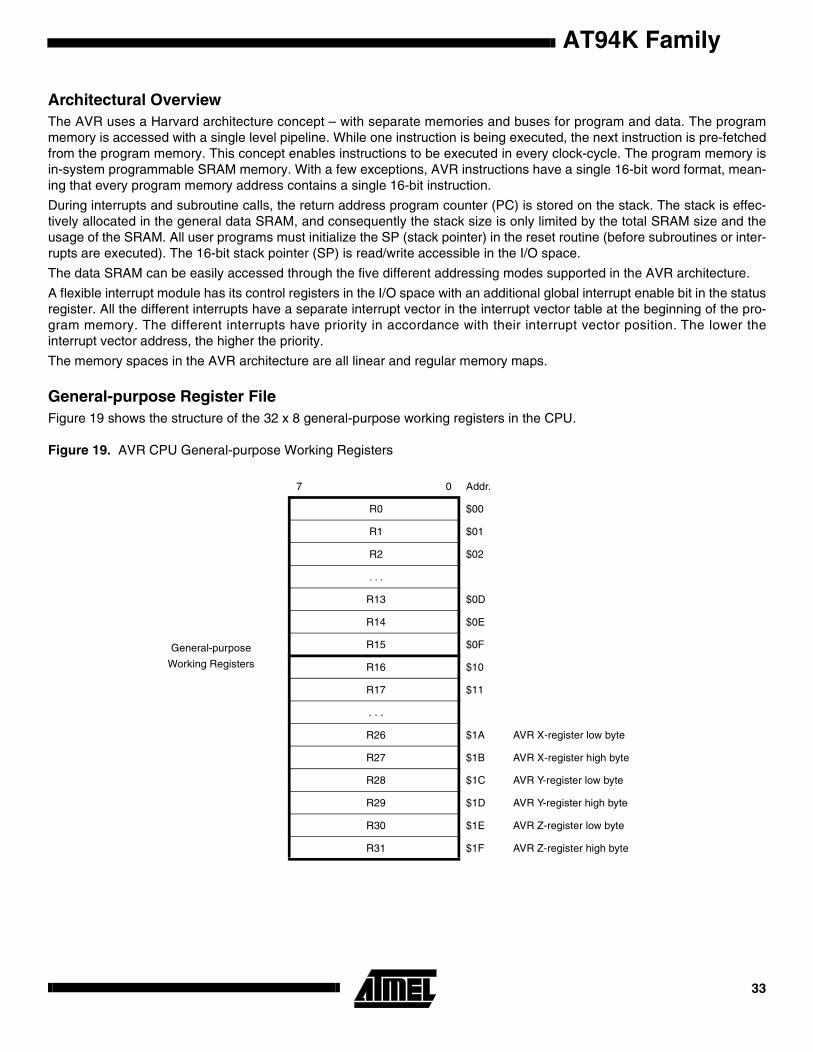
General-purpose Register FileFigure 19 shows the structure of the 32 x 8 general-purpose working registers in the CPU.
Figure 19. AVR CPU General-purpose Working Registers
7 0 Addr.
R0 $00
R1 $01
R2 $02
. . .
R13 $0D
General-purpose
Working Registers
R14 $0E
R15 $0F
R16 $10
R17 $11
. . .
R26 $1A AVR X-register low byte
R27 $1B AVR X-register high byte
R28 $1C AVR Y-register low byte
R29 $1D AVR Y-register high byte
R30 $1E AVR Z-register low byte
R31 $1F AVR Z-register high byte
33
All the register operating instructions in the instruction set have direct- and single-cycle access to all registers. The onlyexception is the five constant arithmetic and logic instructions SBCI, SUBI, CPI, ANDI and ORI between a constant and aregister and the LDI instruction for load-immediate constant data. These instructions apply to the second half of the regis-ters in the register file – R16..R31. The general SBC, SUB, CP, AND and OR and all other operations between tworegisters or on a single-register apply to the entire register file.
As shown in Figure 5 each register is also assigned a data memory address, mapping them directly into the first 32 loca-tions of the user Data Space. Although not being physically implemented as SRAM locations, this memory organizationprovides great flexibility in access of the registers, as the X,Y and Z registers can be set to index any register in the file.
The 4K to 16K bytes of data SRAM, as configured during FPSLIC download, are available for general data are imple-mented starting at address $0060 as follows:
Addresses beyond the maximum amount of data SRAM are unavailable for write or read and will return unknown data ifaccessed. Ghost memory is not implemented.
X-register, Y-register and Z-registerThe registers R26..R31 have some added functions to their general-purpose usage. These registers are address pointersfor indirect addressing of the SRAM. The three indirect address registers X, Y and Z have functions as fixed displacement,automatic increment and decrement (see the descriptions for the different instructions).
ALU – Arithmetic Logic UnitThe high-performance AVR ALU operates in direct connection with all the 32 general-purpose working registers. Within asingle-clock-cycle, ALU operations between registers in the register file are executed. The ALU operations are divided intothree main categories – arithmetic, logical and bit-functions.
Multiplier UnitThe high-performance AVR Multiplier operates in direct connection with all the 32 general-purpose working registers. Thisunit performs 8 x 8 multipliers every two clock cycles.
SRAM Data MemoryExternal data SRAM (or program) cannot be used with the FPSLIC AT94K family.
The five different addressing modes for the data memory cover: Direct, Indirect with Displacement, Indirect, Indirect withPre-decrement and Indirect with Post-increment. In the register file, registers R26 to R31 feature the indirect addressingpointer registers.
The Indirect with Displacement mode features a 63 address locations reach from the base address given by the Y orZ-register.
When using register indirect addressing modes with automatic Pre-decrement and Post-increment, the address registersX, Y and Z are decremented and incremented.
The entire data address space including the 32 general-purpose working registers and the 64 I/O registers are all accessi-ble through all these addressing modes. See the next section for a detailed description of the different addressing modes.
4K $0060 : $0FFF
8K $0060 : $1FFF
12K $0060 : $2FFF
16K $0060 : $3FFF
AT94K Family34
AT94K Family
Program and Data Addressing ModesThe embedded AVR core supports powerful and efficient addressing modes for access to the program memory (SRAM)and data memory (SRAM, Register File and I/O Memory). This section describes the different addressing modes supportedby the AVR architecture.
Register Direct, Single-register RdThe operand is contained in register d (Rd).
Register Direct, Two Registers Rd and RrOperands are contained in register r (Rr) and d (Rd). The result is stored in register d (Rd).
I/O DirectOperand address is contained in 6 bits of the instruction word. n is the destination or source register address.
Data DirectA 16-bit data address is contained in the 16 LSBs of a two-word instruction. Rd/Rr specify the destination or sourceregister.
Data Indirect with DisplacementOperand address is the result of the Y or Z-register contents added to the address contained in 6 bits of the instructionword.
Data IndirectOperand address is the contents of the X, Y or the Z-register.
Data Indirect with Pre-decrementThe X, Y or the Z-register is decremented before the operation. Operand address is the decremented contents of the X, Yor the Z-register.
Data Indirect with Post-incrementThe X, Y or the Z-register is incremented after the operation. Operand address is the content of the X, Y or the Z-registerprior to incrementing.
Direct Program Address, JMP and CALLProgram execution continues at the address immediate in the instruction words.
Indirect Program Addressing, IJMP and ICALLProgram execution continues at address contained by the Z-register (i.e. the PC is loaded with the contents of theZ-register).
Relative Program Addressing, RJMP and RCALLProgram execution continues at address PC + k + 1. The relative address k is -2048 to 2047.
35
Memory Access Times and Instruction Execution TimingThis section describes the general access timing concepts for instruction execution and internal memory access.
The AVR CPU is driven by the XTAL1 input directly generated from the external clock crystal for the chip. No internal clockdivision is used.
Figure 20 shows the parallel instruction fetches and instruction executions enabled by the Harvard architecture and thefast-access register file concept. This is the basic pipelining concept to obtain up to 1 MIPS per MHz with the correspondingunique results for functions per cost, functions per clocks, and functions per power-unit.
Figure 21 shows the internal timing concept for the register file. In a single-clock-cycle an ALU operation using two registeroperands is executed, and the result is stored back to the destination register.
Figure 20. The Parallel Instruction Fetches and Instruction Executions
Figure 21. Single Cycle ALU Operation
AVR CLK
1st Instruction Fetch
1st Instruction Execute2nd Instruction Fetch
2nd Instruction Execute3rd Instruction Fetch
3rd Instruction Execute4th Instruction Fetch
T1 T2 T3 T4
AVR CLK
Total Execution Time
Register Operands Fetch
ALU Operation Execute
Result Write Back
T1 T2 T3 T4
AT94K Family36

AT94K Family
The internal data SRAM access is performed in two system clock cycles as described in Figure 22.
Figure 22. On-chip Data SRAM Access Cycles
AVR CLK
WR
RD
Data
Data
Address Address
T1 T2 T3 T4
Prev. Address
Rea
dW
rite
37

Memory-mapped I/OThe I/O space definition of the embedded AVR core is shown in the following table.
AT94K40/20/10 Register Summary
Address Name Bit 7 Bit 6 Bit 5 Bit 4 Bit 3 Bit 2 Bit 1 Bit 0
$3F ($5F) SREG I T H S V N Z C
$3E ($5E) SPH SP15 SP14 SP13 SP12 SP11 SP10 SP9 SP8
$3D ($5D) SPL SP7 SP6 SP5 SP4 SP3 SP2 SP1 SP0
$3C ($5C) Reserved
$3B ($5B) EIMF INTF7 INTF5 INTF3 INTF1 INT7 INT5 INT3 INT1
$3A ($5A) SFTCR SRST
$39 ($59) TIMSK TOIE1 OCIE1A OCIE13 TOIE2 TICIE1 OCIE2 TOIE0 OCIE0
$38 ($58) TIFR TOV1 OCF1A OCF1B TOV2 ICF1 OCF2 TOV0 OCF0
$37 ($57) Reserved
$36 ($56) I2CR I2INT I2EA I2STA I2STO I2WC I2EN I2IE
$35 ($55) MCUR SE SM1 SM0 WDRF EXTRF
$34 ($54) Reserved
$33 ($53) TCCR0 FOC0 PWM0 COM01 COM00 CTC0 CS02 CS01 CS00
$32 ($52) TCNT0 Timer/Counter0 (8-bit)
$31 ($51) OCR0 Timer/Counter0 Output Compare Register
$30 ($50) SFIOR PSR2 PSR10
$2F ($4F) TCCR1A COM1A1 COM1A0 COM1B1 COM1B0 FOC1A FOC1B PWM11 PWM10
$2E ($4E) TCCR1B ICNC1 ICES1 ICPE CTC1 CS12 CS11 CS10
$2D ($4D) TCNT1H Timer/Counter1 - Counter Register High Byte
$2C ($4C) TCNT1L Timer/Counter1 - Counter Register Low Byte
$2B ($4B) OCR1AH Timer/Counter1 - Output Compare Register A High Byte
$2A ($4A) OCR1AL Timer/Counter1 - Output Compare Register A Low Byte
$29 ($49) OCR1BH Timer/Counter1 - Output Compare Register B High Byte
$28 ($48) OCR1BL Timer/Counter1 - Output Compare Register B Low Byte
$27 ($47) TCCR2 FOC2 PWM2 COM21 COM20 CTC2 CS22 CS21 CS20
$26 ($46) ASSR AS2 TCN20B OCR2UB TCR2UB
$25 ($45) ICR1H Timer/Counter1 - Input Capture Register High Byte
$24 ($44) ICR1L Timer/Counter1 - Input Capture Register Low Byte
$23 ($43) TCNT2 Timer/Counter2 (8-bit)
$22 ($42) OCR2 Timer/Counter 2 Output Compare Register
$21 ($41) WDTCR WDTOE WDE WDP2 WDP1 WDP0
$20 ($40) UBRRHI UBRR1[11] UBRR1[10] UBRR1[9] UBRR1[8] UBRR0[11] UBRR0[10] UBRR0[9] UBRR0[8]
$1F ($3F) I2DR 2-wire Serial Data Register
$1E ($3E) I2AR 2-wire Serial Address Register
$1D ($3D) I2SR 2-wire Serial Status Register
$1C ($3C) I2BR 2-wire Serial Bit Rate Register
$1B ($3B) FPGAD FPGA Cache Data Register (D7 - D0)
$1A ($3A) FPGAZ FPGA Cache Z Address Register (T3 - T0) (Z3 - Z0)
$19 ($39) FPGAY FPGA Cache Y Address Register (47 - 40)
$18 ($38) FPGAX FPGA Cache X Address Register (X7 - X0)
$17 ($37) FISUD FPGA I/O Select, Interrupt Mask/Flag Register D
AT94K Family38

AT94K Family
All the different embedded AVR core I/Os and peripherals are placed in the I/O space. All FPGA virtual peripherals areplaced in the I/O space. The different I/O locations are directly accessed by the IN and OUT instructions transferring databetween the 32 x 8 general-purpose working registers and the I/O space. I/O registers within the address range $00 - $1Fare directly bit-accessible using the SBI and CBI instructions. In these registers, the value of single bits can be checked byusing the SBIS and SBIC instructions. When using the I/O specific instructions IN, OUT, the I/O register address $00 - $3Fare used. When addressing I/O registers as SRAM, $20 must be added to this address. All I/O register addresses through-out this document are shown with the SRAM address in parentheses.
$16 ($36) FISUC FPGA I/O Select, Interrupt Mask/Flag Register C
$15 ($35) FISUB FPGA I/O Select, Interrupt Mask/Flag Register B
$14 ($34) FISUA FPGA I/O Select, Interrupt Mask/Flag Register A
$13 ($33) FISCR FIADR XFIS1 XFIS0
$12 ($32) PORTD PORTD7 PORTD6 PORTD5 PORTD4 PORTD3 PORTD2 PORTD1 PORTD0
$11 ($31) DDRD DDRD7 DDRD6 DDRD5 DDRD4 DDRD3 DDRD2 DDRD1 DDRD0
$10 ($30) PIND PIND7 PIND6 PIND5 PIND4 PIND3 PIND2 PIND1 PIND0
$0F ($2F) Reserved
$0E ($2E) Reserved
$0D ($2D) Reserved
$0C ($2C) UDR0 UART0 I/O Data Register
$0B ($2B) USCR0A RXC0 TXC0 UCRE0 FE0 OR0 U2X0 MPCM0
$0A ($2A) USCR0B RXCIE0 TXCIE0 UDRIE0 RXEN0 TXEN0 CHR90 RXB80 TXB80
$09 ($29) UBRR0 UART0 Baud-rate Register
$08 ($28) Reserved
$07 ($27) PORTE PORTE7 PORTE6 PORTE5 PORTE4 PORTE3 PORTE2 PORTE1 PORTE0
$06 ($26) DDRE DDRE7 DDRE6 DDRE5 DDRE4 DDRE3 DDRE2 DDRE1 DDRE0
$05 ($25) PINE PINE7 PINE6 PINE5 PINE4 PINE3 PINE2 PINE1 PINE0
$04 ($24) Reserved
$03 ($23) UDR1 UART1 I/O Data Register
$02 ($22) USCR1A RXC1 TXC1 UCRE1 FE1 OR1 U2X1 MPCM1
$01 ($21) USCR1B RXCIE1 TXCIE1 UDRIE1 RXEN1 TXEN1 CHR91 RXB81 TXB81
$00 ($20) UBRR1 UART1 Baud-rate Register
AT94K40/20/10 Register Summary (Continued)
Address Name Bit 7 Bit 6 Bit 5 Bit 4 Bit 3 Bit 2 Bit 1 Bit 0
39
Figure 23. Memory-mapped I/O
For single-cycle access (In/Out Commands) to I/O, the instruction has to be less than 16 bits:
In the data SRAM, the registers are located at memory addresses $00 - $1F and the I/O space is located at memoryaddresses $20 - $5F.
As there are only 6 bits available to refer to the I/O space, the address is shifted down 2 bits. This means the In/Out com-mands access $00 to $3F which goes directly to the I/O and maps to $20 to $5F in SRAM. All other instructions access theI/O space through the $20 - 5F addressing.
For compatibility with future devices, reserved bits should be written to zero if accessed. Reserved I/O memory addressesshould never be written.
The status flags are cleared by writing a logical one to them. Note that the CBI and SBI instructions will operate on all bitsin the I/O register, writing a one back into any flag read as set, thus clearing the flag. The CBI and SBI instructions workwith registers $00 to $1F only.
The different I/O and peripherals control registers are explained in the following sections.
opcode register address
5 bitsr0 - 31 ($1F)5 bits
r0 - 63 ($3F)6 bits
$00
$1F
$5FSRAM Space
I/O Space
$00
$3F Memory-mappedI/O
Registers r0 - r31
Used for In/OutInstructions
Used for allOther Instructions
AT94K Family40
AT94K Family
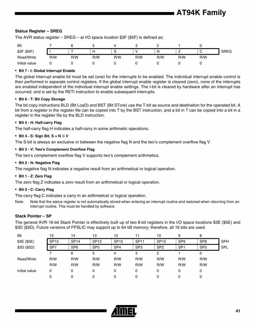
Status Register – SREG
The AVR status register – SREG – at I/O space location $3F ($5F) is defined as:
• Bit 7 - I: Global Interrupt Enable
The global interrupt enable bit must be set (one) for the interrupts to be enabled. The individual interrupt enable control isthen performed in separate control registers. If the global interrupt enable register is cleared (zero), none of the interruptsare enabled independent of the individual interrupt enable settings. The I-bit is cleared by hardware after an interrupt hasoccurred, and is set by the RETI instruction to enable subsequent interrupts.
• Bit 6 - T: Bit Copy Storage
The bit copy instructions BLD (Bit LoaD) and BST (Bit STore) use the T-bit as source and destination for the operated bit. Abit from a register in the register file can be copied into T by the BST instruction, and a bit in T can be copied into a bit in aregister in the register file by the BLD instruction.
• Bit 5 - H: Half-carry Flag
The half-carry flag H indicates a half-carry in some arithmetic operations.
• Bit 4 - S: Sign Bit, S = N ⊕ V
The S-bit is always an exclusive or between the negative flag N and the two’s complement overflow flag V.
• Bit 3 - V: Two’s Complement Overflow Flag
The two’s complement overflow flag V supports two’s complement arithmetics.
• Bit 2 - N: Negative Flag
The negative flag N indicates a negative result from an arithmetical or logical operation.
• Bit 1 - Z: Zero Flag
The zero flag Z indicates a zero result from an arithmetical or logical operation.
• Bit 0 - C: Carry Flag
The carry flag C indicates a carry in an arithmetical or logical operation. Note: Note that the status register is not automatically stored when entering an interrupt routine and restored when returning from an
interrupt routine. This must be handled by software.
Stack Pointer – SP
The general AVR 16-bit Stack Pointer is effectively built up of two 8-bit registers in the I/O space locations $3E ($5E) and$3D ($5D). Future versions of FPSLIC may support up to 64 kB memory; therefore, all 16 bits are used.
Bit 7 6 5 4 3 2 1 0
$3F ($5F) I T H S V N Z C SREG
Read/Write R/W R/W R/W R/W R/W R/W R/W R/W
Initial value 0 0 0 0 0 0 0 0
Bit 15 14 13 12 11 10 9 8
$3E ($5E) SP15 SP14 SP13 SP12 SP11 SP10 SP9 SP8 SPH
$3D ($5D) SP7 SP6 SP5 SP4 SP3 SP2 SP1 SP0 SPL
7 6 5 4 3 2 1 0
Read/Write R/W R/W R/W R/W R/W R/W R/W R/W
R/W R/W R/W R/W R/W R/W R/W R/W
Initial value 0 0 0 0 0 0 0 0
0 0 0 0 0 0 0 0
41

The Stack Pointer points to the data SRAM stack area where the Subroutine and Interrupt Stacks are located. This Stackspace in the data SRAM must be defined by the program before any subroutine calls are executed or interrupts areenabled. The stack pointer must be set to point above $60. The Stack Pointer is decremented by one when data is pushedonto the Stack with the PUSH instruction, and it is decremented by two when an address is pushed onto the Stack withsubroutine calls and interrupts. The Stack Pointer is incremented by one when data is popped from the Stack with the POPinstruction, and it is incremented by two when an address is popped from the Stack with return from subroutine RET orreturn from interrupt RETI.
Software Control of System Configuration
The software control register will allow the software to manage select system level configuration bits. Currently, only resetcontrol by software is available.
Software Control Register – SFTCR
• Bit 7..1 - Res: Reserved Bits
These bits are reserved in the AT94K and always read as 0.
• Bit 0 - SRST: Software Reset
When this bit is set to 1, a reset request is sent to the system configuration. Appropriate reset signals are generated andconfiguration download is initiated. During AVR reset, the SRST bit is cleared by hardware.
MCU Control Status/Register – MCUR
The MCU Register contains control bits for general MCU functions and status bits to indicate the source of an MCU reset.
• Bit 5 - SE: Sleep Enable
The SE bit must be set (one) to make the MCU enter the Sleep mode when the SLEEP instruction is executed. To avoidthe MCU entering the Sleep mode unless it is the programmers purpose, it is recommended to set the Sleep Enable SE bitjust before the execution of the SLEEP instruction.
• Bits 4, 3 - SM1/SM0: Sleep Mode Select Bits 1 and 0
This bit selects between the three available Sleep modes as shown in Table 3.
• Bits 2 - Res: Reserved Bit
This bit is reserved in the AT94K and will always read zero.
• Bit 1 - WDRF: Watchdog Reset Flag
This bit is set if a watchdog reset occurs. The bit is cleared by writing a logic zero to the flag.
Bit 7 6 5 4 3 2 1 0
$3A ($5A) - - - - - - - SRST
Read/Write R R R R R R R R/W
Initial value 0 0 0 0 0 0 0 0
Bit 5 4 3 2 1 0
$35 ($55) SE SM1 SM0 - WDRF EXTRF MCUR
Read/Write R/W R/W R/W R R R
Initial value 0 0 0 0 0 0
AT94K Family42
AT94K Family
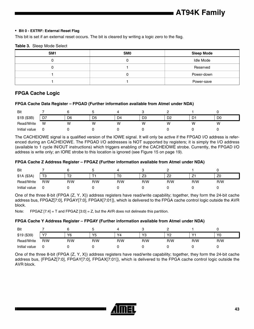
• Bit 0 - EXTRF: External Reset Flag
This bit is set if an external reset occurs. The bit is cleared by writing a logic zero to the flag.
FPGA Cache Logic
FPGA Cache Data Register – FPGAD (Further information available from Atmel under NDA)
The CACHEIOWE signal is a qualified version of the IOWE signal. It will only be active if the FPGAD I/O address is refer-enced during an CACHEIOWE. The FPGAD I/O addresses is NOT supported by registers; it is simply the I/O address(available to 1 cycle IN/OUT instructions) which triggers enabling of the CACHEIOWE strobe. Currently, the FPGAD I/Oaddress is write only; an IORE strobe to this location is ignored (see Figure 15 on page 19).
FPGA Cache Z Address Register – FPGAZ (Further information available from Atmel under NDA)
One of the three 8-bit (FPGA {Z, Y, X}) address registers have read/write capability; together, they form the 24-bit cacheaddress bus, FPGAZ[7:0], FPGAY[7:0], FPGAX[7:01]}, which is delivered to the FPGA cache control logic outside the AVRblock.
Note: FPGAZ [7:4] = T and FPGAZ [3:0] = Z, but the AVR does not delineate this partition.
FPGA Cache Y Address Register – FPGAY (Further information available from Atmel under NDA)
One of the three 8-bit (FPGA {Z, Y, X}) address registers have read/write capability; together, they form the 24-bit cacheaddress bus, {FPGAZ[7:0], FPGAY[7:0], FPGAX[7:01]}, which is delivered to the FPGA cache control logic outside theAVR block.
Table 3. Sleep Mode Select
SM1 SM0 Sleep Mode
0 0 Idle Mode
0 1 Reserved
1 0 Power-down
1 1 Power-save
Bit 7 6 5 4 3 2 1 0
$1B ($3B) D7 D6 D5 D4 D3 D2 D1 D0
Read/Write W W W W W W W W
Initial value 0 0 0 0 0 0 0 0
Bit 7 6 5 4 3 2 1 0
$1A ($3A) T3 T2 T1 T0 Z3 Z2 Z1 Z0
Read/Write R/W R/W R/W R/W R/W R/W R/W R/W
Initial value 0 0 0 0 0 0 0 0
Bit 7 6 5 4 3 2 1 0
$19 ($39) Y7 Y6 Y5 Y4 Y3 Y2 Y1 Y0
Read/Write R/W R/W R/W R/W R/W R/W R/W R/W
Initial value 0 0 0 0 0 0 0 0
43

FPGA Cache X Address Register – FPGAX (Further information available from Atmel under NDA)
One of the three 8-bit (FPGA {Z, Y, X}) address registers have read/write capability; together, they form the 24-bit cacheaddress bus, {FPGAZ[7:0], FPGAY[7:0], FPGAX[7:01}, which is delivered to the FPGA cache control logic outside the AVRblock.
FPGA I/O Selection by AVRSixteen select signals are sent to the FPGA for I/O addressing. These signals are decoded from four I/O registry addresses(FISU{D, C, B, A}) and extended to sixteen with two bits from the FPGA I/O Select Control Register (FISCR). In addition,the FPGAIORE and FPGAIOWE signals are qualified versions of the IORE and IOWE signals. Each will only be active ifone of the four base I/O addresses are referenced. It remains the responsibility of the FPGA Designer to implementany necessary registers for each select line. Only the FISCR registers physically exist. The FISU {A, B, C, D} I/Oaddresses for the purpose of FPGA I/O selection are NOT supported by AVR Core I/O space registers; they are simply I/Oaddresses (available to 1 cycle IN/OUT instructions) which trigger appropriate enabling of the FPGA select lines and theFPGA IORE/IOWE strobes (see Figure 12 on page 15).
FPGA I/O Select Control Register – FISCR
• Bit 7 - FIADR: FPGA Interrupt Addressing Enable
When FIADR is set to 1 accessing FISUD$17($37)-FISUA$14($34) will access the FPGA interrupt Mask/Flag Registers inthe normal AVR register space. When FIADR is set to 0 accessing FISUD-FISUA will enable one of four groups of fourselect signals set to the FPGA. The current XFIS[1:0] bit values determine which signal in the group is selected (seebelow). The FIADR bit is cleared during reset.
• Bit 6..2 - Res: Reserved Bits
These bits are reserved in the AT94K and always read as 0.
• Bit 1 - XFIS1: Extended FPGA I/O Select Bit 1
Bit 7 6 5 4 3 2 1 0
$18 ($38) X7 X6 X5 X4 X3 X2 X1 X0
Read/Write R/W R/W R/W R/W R/W R/W R/W R/W
Initial value 0 0 0 0 0 0 0 0
Bit 7 6 5 4 3 2 1 0
$13 ($33) FIADR - - - - - XFIS1 XFIS0
Read/Write R/W R R R R R R/W R/W
Initial value 0 0 0 0 0 0 0 0
AT94K Family44
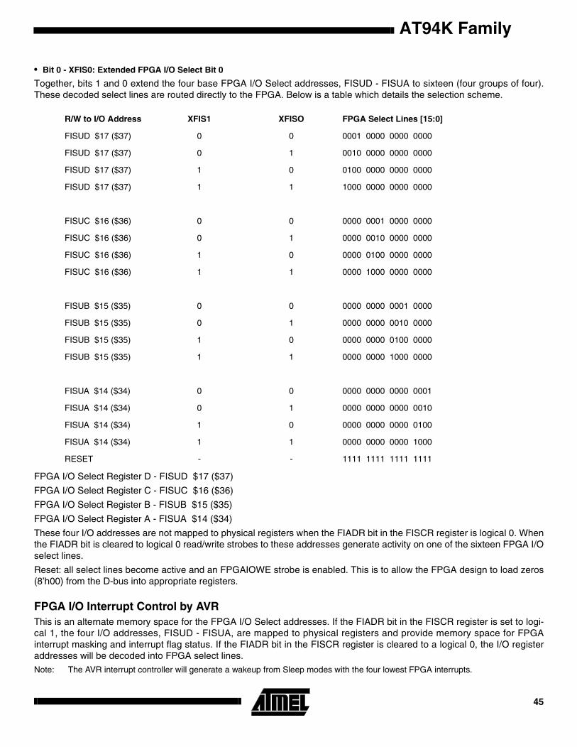
AT94K Family
• Bit 0 - XFIS0: Extended FPGA I/O Select Bit 0
Together, bits 1 and 0 extend the four base FPGA I/O Select addresses, FISUD - FISUA to sixteen (four groups of four).These decoded select lines are routed directly to the FPGA. Below is a table which details the selection scheme.
FPGA I/O Select Register D - FISUD $17 ($37)
FPGA I/O Select Register C - FISUC $16 ($36)
FPGA I/O Select Register B - FISUB $15 ($35)
FPGA I/O Select Register A - FISUA $14 ($34)
These four I/O addresses are not mapped to physical registers when the FIADR bit in the FISCR register is logical 0. Whenthe FIADR bit is cleared to logical 0 read/write strobes to these addresses generate activity on one of the sixteen FPGA I/Oselect lines.
Reset: all select lines become active and an FPGAIOWE strobe is enabled. This is to allow the FPGA design to load zeros(8’h00) from the D-bus into appropriate registers.
FPGA I/O Interrupt Control by AVRThis is an alternate memory space for the FPGA I/O Select addresses. If the FIADR bit in the FISCR register is set to logi-cal 1, the four I/O addresses, FISUD - FISUA, are mapped to physical registers and provide memory space for FPGAinterrupt masking and interrupt flag status. If the FIADR bit in the FISCR register is cleared to a logical 0, the I/O registeraddresses will be decoded into FPGA select lines.
Note: The AVR interrupt controller will generate a wakeup from Sleep modes with the four lowest FPGA interrupts.
R/W to I/O Address XFIS1 XFISO FPGA Select Lines [15:0]
FISUD $17 ($37) 0 0 0001 0000 0000 0000
FISUD $17 ($37) 0 1 0010 0000 0000 0000
FISUD $17 ($37) 1 0 0100 0000 0000 0000
FISUD $17 ($37) 1 1 1000 0000 0000 0000
FISUC $16 ($36) 0 0 0000 0001 0000 0000
FISUC $16 ($36) 0 1 0000 0010 0000 0000
FISUC $16 ($36) 1 0 0000 0100 0000 0000
FISUC $16 ($36) 1 1 0000 1000 0000 0000
FISUB $15 ($35) 0 0 0000 0000 0001 0000
FISUB $15 ($35) 0 1 0000 0000 0010 0000
FISUB $15 ($35) 1 0 0000 0000 0100 0000
FISUB $15 ($35) 1 1 0000 0000 1000 0000
FISUA $14 ($34) 0 0 0000 0000 0000 0001
FISUA $14 ($34) 0 1 0000 0000 0000 0010
FISUA $14 ($34) 1 0 0000 0000 0000 0100
FISUA $14 ($34) 1 1 0000 0000 0000 1000
RESET - - 1111 1111 1111 1111
45
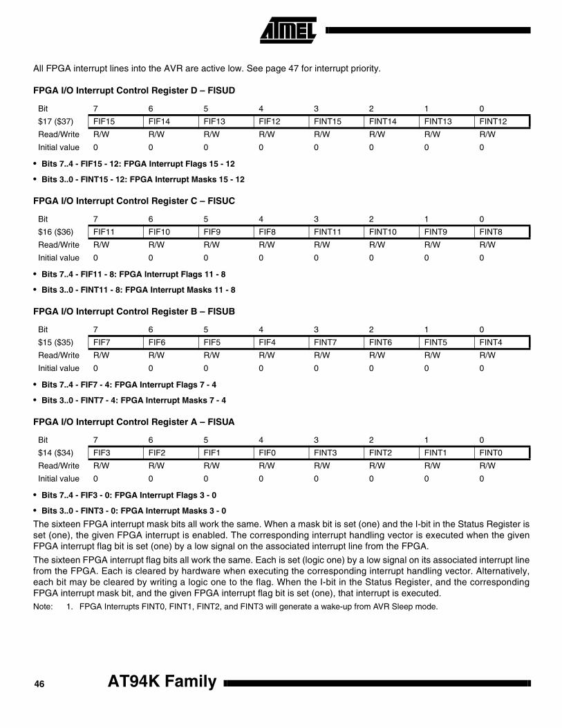
All FPGA interrupt lines into the AVR are active low. See page 47 for interrupt priority.
FPGA I/O Interrupt Control Register D – FISUD
• Bits 7..4 - FIF15 - 12: FPGA Interrupt Flags 15 - 12
• Bits 3..0 - FINT15 - 12: FPGA Interrupt Masks 15 - 12
FPGA I/O Interrupt Control Register C – FISUC
• Bits 7..4 - FIF11 - 8: FPGA Interrupt Flags 11 - 8
• Bits 3..0 - FINT11 - 8: FPGA Interrupt Masks 11 - 8
FPGA I/O Interrupt Control Register B – FISUB
• Bits 7..4 - FIF7 - 4: FPGA Interrupt Flags 7 - 4
• Bits 3..0 - FINT7 - 4: FPGA Interrupt Masks 7 - 4
FPGA I/O Interrupt Control Register A – FISUA
• Bits 7..4 - FIF3 - 0: FPGA Interrupt Flags 3 - 0
• Bits 3..0 - FINT3 - 0: FPGA Interrupt Masks 3 - 0
The sixteen FPGA interrupt mask bits all work the same. When a mask bit is set (one) and the I-bit in the Status Register isset (one), the given FPGA interrupt is enabled. The corresponding interrupt handling vector is executed when the givenFPGA interrupt flag bit is set (one) by a low signal on the associated interrupt line from the FPGA.
The sixteen FPGA interrupt flag bits all work the same. Each is set (logic one) by a low signal on its associated interrupt linefrom the FPGA. Each is cleared by hardware when executing the corresponding interrupt handling vector. Alternatively,each bit may be cleared by writing a logic one to the flag. When the I-bit in the Status Register, and the correspondingFPGA interrupt mask bit, and the given FPGA interrupt flag bit is set (one), that interrupt is executed.Note: 1. FPGA Interrupts FINT0, FINT1, FINT2, and FINT3 will generate a wake-up from AVR Sleep mode.
Bit 7 6 5 4 3 2 1 0
$17 ($37) FIF15 FIF14 FIF13 FIF12 FINT15 FINT14 FINT13 FINT12
Read/Write R/W R/W R/W R/W R/W R/W R/W R/W
Initial value 0 0 0 0 0 0 0 0
Bit 7 6 5 4 3 2 1 0
$16 ($36) FIF11 FIF10 FIF9 FIF8 FINT11 FINT10 FINT9 FINT8
Read/Write R/W R/W R/W R/W R/W R/W R/W R/W
Initial value 0 0 0 0 0 0 0 0
Bit 7 6 5 4 3 2 1 0
$15 ($35) FIF7 FIF6 FIF5 FIF4 FINT7 FINT6 FINT5 FINT4
Read/Write R/W R/W R/W R/W R/W R/W R/W R/W
Initial value 0 0 0 0 0 0 0 0
Bit 7 6 5 4 3 2 1 0
$14 ($34) FIF3 FIF2 FIF1 FIF0 FINT3 FINT2 FINT1 FINT0
Read/Write R/W R/W R/W R/W R/W R/W R/W R/W
Initial value 0 0 0 0 0 0 0 0
AT94K Family46
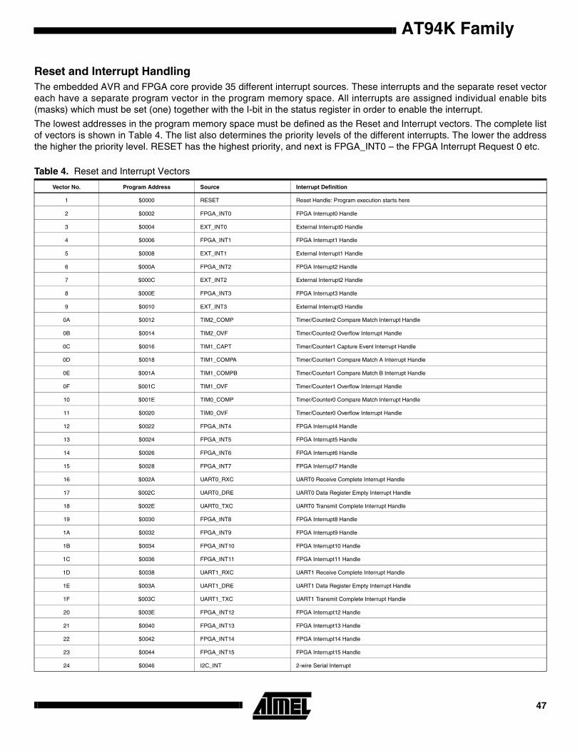
AT94K Family
Reset and Interrupt HandlingThe embedded AVR and FPGA core provide 35 different interrupt sources. These interrupts and the separate reset vectoreach have a separate program vector in the program memory space. All interrupts are assigned individual enable bits(masks) which must be set (one) together with the I-bit in the status register in order to enable the interrupt.
The lowest addresses in the program memory space must be defined as the Reset and Interrupt vectors. The complete listof vectors is shown in Table 4. The list also determines the priority levels of the different interrupts. The lower the addressthe higher the priority level. RESET has the highest priority, and next is FPGA_INT0 – the FPGA Interrupt Request 0 etc.
Table 4. Reset and Interrupt Vectors
Vector No. Program Address Source Interrupt Definition
1 $0000 RESET Reset Handle: Program execution starts here
2 $0002 FPGA_INT0 FPGA Interrupt0 Handle
3 $0004 EXT_INT0 External Interrupt0 Handle
4 $0006 FPGA_INT1 FPGA Interrupt1 Handle
5 $0008 EXT_INT1 External Interrupt1 Handle
6 $000A FPGA_INT2 FPGA Interrupt2 Handle
7 $000C EXT_INT2 External Interrupt2 Handle
8 $000E FPGA_INT3 FPGA Interrupt3 Handle
9 $0010 EXT_INT3 External Interrupt3 Handle
0A $0012 TIM2_COMP Timer/Counter2 Compare Match Interrupt Handle
0B $0014 TIM2_OVF Timer/Counter2 Overflow Interrupt Handle
0C $0016 TIM1_CAPT Timer/Counter1 Capture Event Interrupt Handle
0D $0018 TIM1_COMPA Timer/Counter1 Compare Match A Interrupt Handle
0E $001A TIM1_COMPB Timer/Counter1 Compare Match B Interrupt Handle
0F $001C TIM1_OVF Timer/Counter1 Overflow Interrupt Handle
10 $001E TIM0_COMP Timer/Counter0 Compare Match Interrupt Handle
11 $0020 TIM0_OVF Timer/Counter0 Overflow Interrupt Handle
12 $0022 FPGA_INT4 FPGA Interrupt4 Handle
13 $0024 FPGA_INT5 FPGA Interrupt5 Handle
14 $0026 FPGA_INT6 FPGA Interrupt6 Handle
15 $0028 FPGA_INT7 FPGA Interrupt7 Handle
16 $002A UART0_RXC UART0 Receive Complete Interrupt Handle
17 $002C UART0_DRE UART0 Data Register Empty Interrupt Handle
18 $002E UART0_TXC UART0 Transmit Complete Interrupt Handle
19 $0030 FPGA_INT8 FPGA Interrupt8 Handle
1A $0032 FPGA_INT9 FPGA Interrupt9 Handle
1B $0034 FPGA_INT10 FPGA Interrupt10 Handle
1C $0036 FPGA_INT11 FPGA Interrupt11 Handle
1D $0038 UART1_RXC UART1 Receive Complete Interrupt Handle
1E $003A UART1_DRE UART1 Data Register Empty Interrupt Handle
1F $003C UART1_TXC UART1 Transmit Complete Interrupt Handle
20 $003E FPGA_INT12 FPGA Interrupt12 Handle
21 $0040 FPGA_INT13 FPGA Interrupt13 Handle
22 $0042 FPGA_INT14 FPGA Interrupt14 Handle
23 $0044 FPGA_INT15 FPGA Interrupt15 Handle
24 $0046 I2C_INT 2-wire Serial Interrupt
47

The most typical program setup for the Reset and Interrupt Vector Addresses are:Address Labels Code Comments
$0000 jmp RESET Reset Handle: Program execution starts here
$0002 jmp FPGA_INT0 ; FPGA Interrupt0 Handle
$0004 jmp EXT_INT0 ; External Interrupt0 Handle
$0006 jmp FPGA_INT1 ; FPGA Interrupt1 Handle
$0008 jmp EXT_INT1 ; External Interrupt1 Handle
$000A jmp FPGA_INT2 ; FPGA Interrupt2 Handle
$000C jmp EXT_INT2 ; External Interrupt2 Handle
$000E jmp FPGA_INT3 ; FPGA Interrupt3 Handle
$0010 jmp EXT_INT3 ; External Interrupt3 Handle
$0012 jmp TIM2_COMP ; Timer/Counter2 Compare Match Interrupt Handle
$0014 jmp TIM2_OVF ; Timer/Counter2 Overflow Interrupt Handle
$0016 jmp TIM1_CAPT ; Timer/Counter1 Capture Event Interrupt Handle
$0018 jmp TIM1_COMPA ; Timer/Counter1 Compare Match A Interrupt Handle
$001A jmp TIM1_COMPB ; Timer/Counter1 Compare Match B Interrupt Handle
$001C jmp TIM1_OVF ; Timer/Counter1 Overflow Interrupt Handle
$001E jmp TIM0_COMP ; Timer/Counter0 Compare Match Interrupt Handle
$0020 jmp TIM0_OVF ; Timer/Counter0 Overflow Interrupt Handle
$0022 jmp FPGA_INT4 ; FPGA Interrupt4 Handle
$0024 jmp FPGA_INT5 ; FPGA Interrupt5 Handle
$0026 jmp FPGA_INT6 ; FPGA Interrupt6 Handle
$0028 jmp FPGA_INT7 ; FPGA Interrupt7 Handle
$002A jmp UART0_RXC ; UART0 Receive Complete Interrupt Handle
$002C jmp UART0_DRE ; UART0 Data Register Empty Interrupt Handle
$002E jmp UART0_TXC ; UART0 Transmit Complete Interrupt Handle
$0030 jmp FPGA_INT8 ; FPGA Interrupt8 Handle
$0032 jmp FPGA_INT9 ; FPGA Interrupt9 Handle
$0034 jmp FPGA_INT10 ; FPGA Interrupt10 Handle
$0036 jmp FPGA_INT11 ; FPGA Interrupt11 Handle
$0038 jmp UART1_RXC ; UART1 Receive Complete Interrupt Handle
$003A jmp UART1_DRE ; UART1 Data Register Empty Interrupt Handle
$003C jmp UART1_TXC ; UART1 Transmit Complete Interrupt Handle
$003E jmp FPGA_INT12 ; FPGA Interrupt12 Handle
$0040 jmp FPGA_INT13 ; FPGA Interrupt13 Handle
$0042 jmp FPGA_INT14 ; FPGA Interrupt14 Handle
$0044 jmp FPGA_INT15 ; FPGA Interrupt15 Handle
$0046 jmp I2C_INT ; 2-wire Serial Interrupt
;
$0048 RESET: ldi r16, high(RAMEND); Main program start
$0049 out SPH,r16
$004A ldi r16, low(RAMEND)
$004B out SPL,r16
$004C <instr> xxx
... ... ... ...
AT94K Family48
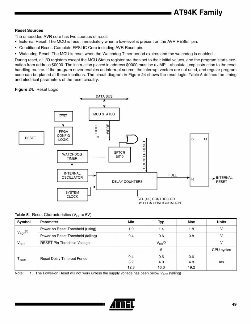
AT94K Family
Reset Sources
The embedded AVR core has two sources of reset:• External Reset. The MCU is reset immediately when a low-level is present on the AVR RESET pin.
• Conditional Reset. Complete FPSLIC Core including AVR Reset pin.
• Watchdog Reset. The MCU is reset when the Watchdog Timer period expires and the watchdog is enabled.
During reset, all I/O registers except the MCU Status register are then set to their initial values, and the program starts exe-cution from address $0000. The instruction placed in address $0000 must be a JMP – absolute jump instruction to the resethandling routine. If the program never enables an interrupt source, the interrupt vectors are not used, and regular programcode can be placed at these locations. The circuit diagram in Figure 24 shows the reset logic. Table 5 defines the timingand electrical parameters of the reset circuitry.
Figure 24. Reset Logic
Note: 1. The Power-on Reset will not work unless the supply voltage has been below VPOT (falling)
MCU STATUS
DATA BUS
RESET
WATCHDOGTIMER
INTERNALOSCILLATOR
SYSTEMCLOCK
DELAY COUNTERS
QS
R INTERNALRESET
POR
CO
UN
TE
R R
ES
ET
SEL [4:0] CONTROLLEDBY FPGA CONFIGURATION
FULL
FPGACONFIGLOGIC
EX
TR
F
WD
RF
SFTCRBIT 0
Table 5. Reset Characteristics (VCC = 5V)
Symbol Parameter Min Typ Max Units
VPOT(1)
Power-on Reset Threshold (rising) 1.0 1.4 1.8 V
Power-on Reset Threshold (falling) 0.4 0.6 0.8 V
VRST RESET Pin Threshold Voltage VCC/2 V
TTOUT Reset Delay Time-out Period
5 CPU cycles
0.43.2
12.8
0.54.0
16.0
0.64.819.2
ms
49
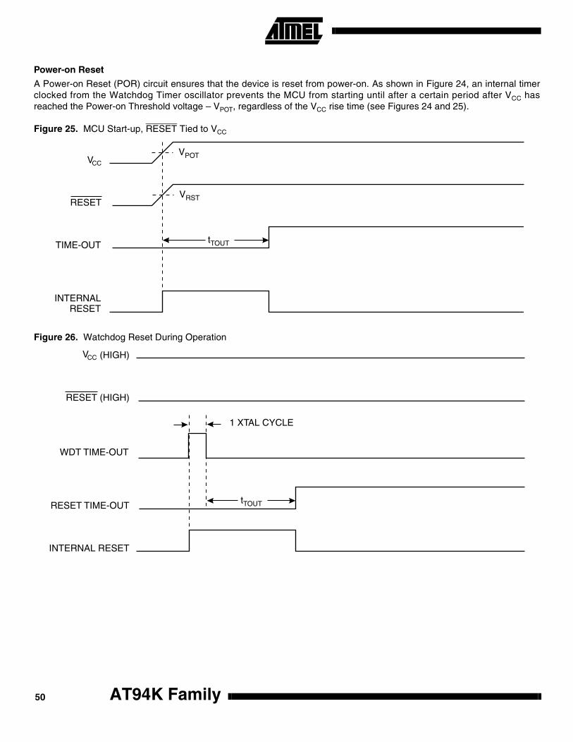
Power-on Reset
A Power-on Reset (POR) circuit ensures that the device is reset from power-on. As shown in Figure 24, an internal timerclocked from the Watchdog Timer oscillator prevents the MCU from starting until after a certain period after VCC hasreached the Power-on Threshold voltage – VPOT, regardless of the VCC rise time (see Figures 24 and 25).
Figure 25. MCU Start-up, RESET Tied to VCC
Figure 26. Watchdog Reset During Operation
V
RESET
TIME-OUT
INTERNALRESET
tTOUT
VPOT
VRST
CC
(HIGH)
RESET (HIGH)
RESET TIME-OUT
INTERNAL RESET
WDT TIME-OUT
tTOUT
1 XTAL CYCLE
VCC
AT94K Family50
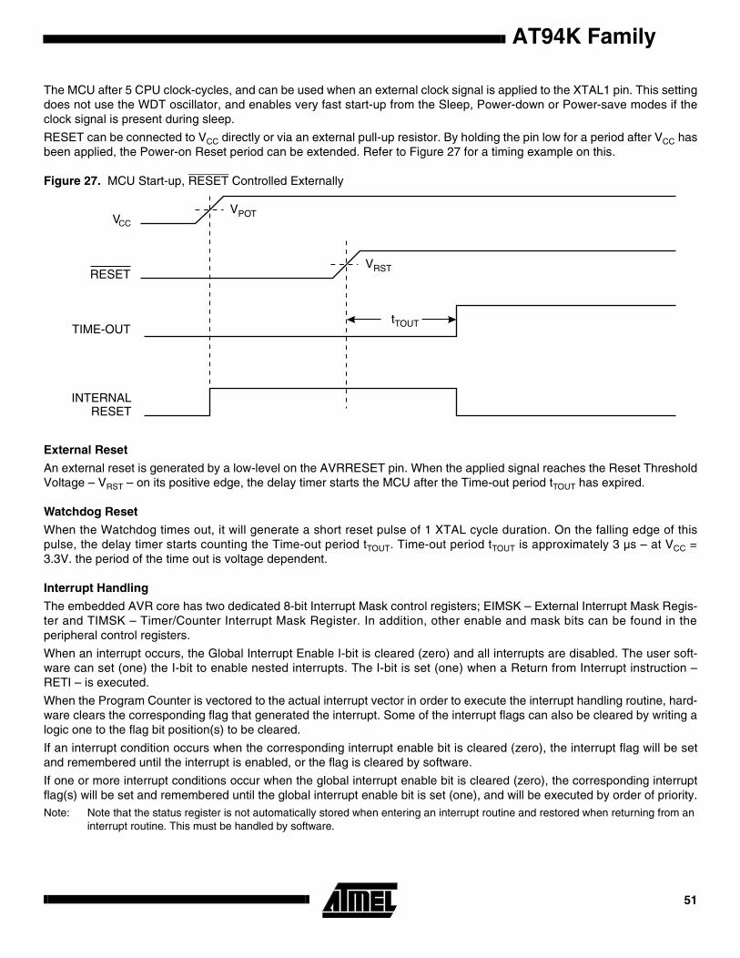
AT94K Family
The MCU after 5 CPU clock-cycles, and can be used when an external clock signal is applied to the XTAL1 pin. This settingdoes not use the WDT oscillator, and enables very fast start-up from the Sleep, Power-down or Power-save modes if theclock signal is present during sleep.
RESET can be connected to VCC directly or via an external pull-up resistor. By holding the pin low for a period after VCC hasbeen applied, the Power-on Reset period can be extended. Refer to Figure 27 for a timing example on this.
Figure 27. MCU Start-up, RESET Controlled Externally
External Reset
An external reset is generated by a low-level on the AVRRESET pin. When the applied signal reaches the Reset ThresholdVoltage – VRST – on its positive edge, the delay timer starts the MCU after the Time-out period tTOUT has expired.
Watchdog Reset
When the Watchdog times out, it will generate a short reset pulse of 1 XTAL cycle duration. On the falling edge of thispulse, the delay timer starts counting the Time-out period tTOUT. Time-out period tTOUT is approximately 3 µs – at VCC =3.3V. the period of the time out is voltage dependent.
Interrupt Handling
The embedded AVR core has two dedicated 8-bit Interrupt Mask control registers; EIMSK – External Interrupt Mask Regis-ter and TIMSK – Timer/Counter Interrupt Mask Register. In addition, other enable and mask bits can be found in theperipheral control registers.
When an interrupt occurs, the Global Interrupt Enable I-bit is cleared (zero) and all interrupts are disabled. The user soft-ware can set (one) the I-bit to enable nested interrupts. The I-bit is set (one) when a Return from Interrupt instruction –RETI – is executed.
When the Program Counter is vectored to the actual interrupt vector in order to execute the interrupt handling routine, hard-ware clears the corresponding flag that generated the interrupt. Some of the interrupt flags can also be cleared by writing alogic one to the flag bit position(s) to be cleared.
If an interrupt condition occurs when the corresponding interrupt enable bit is cleared (zero), the interrupt flag will be setand remembered until the interrupt is enabled, or the flag is cleared by software.
If one or more interrupt conditions occur when the global interrupt enable bit is cleared (zero), the corresponding interruptflag(s) will be set and remembered until the global interrupt enable bit is set (one), and will be executed by order of priority.Note: Note that the status register is not automatically stored when entering an interrupt routine and restored when returning from an
interrupt routine. This must be handled by software.
RESET
TIME-OUT
INTERNALRESET
tTOUT
VPOT
VRST
VCC
51

External Interrupt Mask/Flag Register – EIMF
• Bits 7..4 - INTF3, 2, 1, 0 - INT4: External Interrupt Request Flags Enable
• Bits 3..0 - INT3, 2, 1, 0: External Interrupt Request 3, 2, 1, 0 Enable
When an INT3 - INT0 bit is set (one) and the I-bit in the Status Register (SREG) is set (one), the corresponding external pininterrupt is enabled. The external interrupts are always low-level-triggered interrupts.
• Bits 7..4 - INTF3, 2, 1, 0: External Interrupt 3, 2, 1, 0 Flags
When a low level is detected on the INT3, 2, 1, 0 pins an interrupt request is triggered. The corresponding interrupt flag,INTF3, 2, 1, 0 becomes set (one). If the I-bit in SREG and the corresponding interrupt enable bit, INT3, 2, 1, 0 in EIMF, areset (one), the MCU will jump to the interrupt vector. The flag is cleared when the interrupt routine is executed. Alternatively,the flag is cleared by writing a logical one to it.
Timer/Counter Interrupt Mask Register – TIMSK
• Bit 7 - TOIE1: Timer/Counter1 Overflow Interrupt Enable
When the TOIE1 bit is set (one) and the I-bit in the Status Register is set (one), the Timer/Counter1 Overflow interrupt isenabled. The corresponding interrupt is executed if an overflow in Timer/Counter1 occurs, i.e., when the TOV1 bit is set inthe Timer/Counter Interrupt Flag Register – TIFR.
• Bit 6 - OCIE1A: Timer/Counter1 Output CompareA Match Interrupt Enable
When the OCIE1A bit is set (one) and the I-bit in the Status Register is set (one), the Timer/Counter1 CompareA Matchinterrupt is enabled. The corresponding interrupt is executed if a CompareA match in Timer/Counter1 occurs, i.e., when theOCF1A bit is set in the Timer/Counter Interrupt Flag Register – TIFR.
• Bit 5 - OCIE1B: Timer/Counter1 Output CompareB Match Interrupt Enable
When the OCIE1B bit is set (one) and the I-bit in the Status Register is set (one), the Timer/Counter1 CompareB Matchinterrupt is enabled. The corresponding interrupt is executed if a CompareB match in Timer/Counter1 occurs, i.e., when theOCF1B bit is set in the Timer/Counter Interrupt Flag Register – TIFR.
• Bit 4 - TOIE2: Timer/Counter2 Overflow Interrupt Enable
When the TOIE2 bit is set (one) and the I-bit in the Status Register is set (one), the Timer/Counter2 overflow interrupt isenabled. The corresponding interrupt is executed if an overflow in Timer/Counter2 occurs, i.e., when the TOV2 bit is set inthe Timer/Counter interrupt flag register – TIFR.
• Bit 3 - TICIE1: Timer/Counter1 Input Capture Interrupt Enable
When the TICIE1 bit is set (one) and the I-bit in the Status Register is set (one), the Timer/Counter1 input capture eventinterrupt is enabled. The corresponding interrupt is executed if a capture-triggering event occurs on pin 29, (IC1), i.e., whenthe ICF1 bit is set in the Timer/Counter interrupt flag register – TIFR.
• Bit 2 - OCIE2: Timer/Counter2 Output Compare Interrupt Enable
When the OCIE2 bit is set (one) and the I-bit in the Status Register is set (one), the Timer/Counter2 Compare Match inter-rupt is enabled. The corresponding interrupt is executed if a Compare match in Timer/Counter2 occurs, i.e., when theOCF2 bit is set in the Timer/Counter interrupt flag register – TIFR.
Bit 7 6 5 4 3 2 1 0
$3B ($5B) INTF3 INTF2 INTF1 INTF0 INT3 INT2 INT1 INT0 EIMF
Read/Write R/W R/W R/W R/W R/W R/W R/W R/W
Initial value 0 0 0 0 0 0 0 0
Bit 7 6 5 4 3 2 1 0
$39 ($39) TOIE1 OCIE1A OCIE1B TOIE2 TICIE1 OCIE2 TOIE0 OCIE0 TIMSK
Read/Write R/W R/W R/W R/W R/W R/W R/W R/W
Initial value 0 0 0 0 0 0 0 0
AT94K Family52
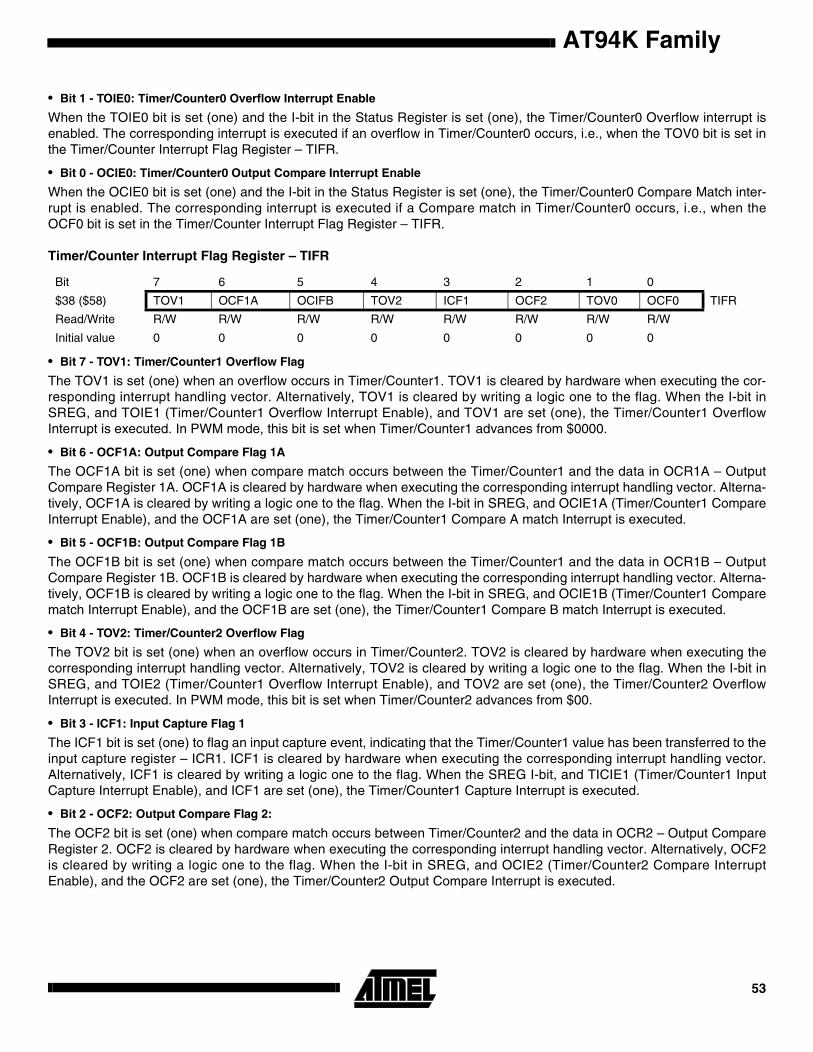
AT94K Family
• Bit 1 - TOIE0: Timer/Counter0 Overflow Interrupt Enable
When the TOIE0 bit is set (one) and the I-bit in the Status Register is set (one), the Timer/Counter0 Overflow interrupt isenabled. The corresponding interrupt is executed if an overflow in Timer/Counter0 occurs, i.e., when the TOV0 bit is set inthe Timer/Counter Interrupt Flag Register – TIFR.
• Bit 0 - OCIE0: Timer/Counter0 Output Compare Interrupt Enable
When the OCIE0 bit is set (one) and the I-bit in the Status Register is set (one), the Timer/Counter0 Compare Match inter-rupt is enabled. The corresponding interrupt is executed if a Compare match in Timer/Counter0 occurs, i.e., when theOCF0 bit is set in the Timer/Counter Interrupt Flag Register – TIFR.
Timer/Counter Interrupt Flag Register – TIFR
• Bit 7 - TOV1: Timer/Counter1 Overflow Flag
The TOV1 is set (one) when an overflow occurs in Timer/Counter1. TOV1 is cleared by hardware when executing the cor-responding interrupt handling vector. Alternatively, TOV1 is cleared by writing a logic one to the flag. When the I-bit inSREG, and TOIE1 (Timer/Counter1 Overflow Interrupt Enable), and TOV1 are set (one), the Timer/Counter1 OverflowInterrupt is executed. In PWM mode, this bit is set when Timer/Counter1 advances from $0000.
• Bit 6 - OCF1A: Output Compare Flag 1A
The OCF1A bit is set (one) when compare match occurs between the Timer/Counter1 and the data in OCR1A – OutputCompare Register 1A. OCF1A is cleared by hardware when executing the corresponding interrupt handling vector. Alterna-tively, OCF1A is cleared by writing a logic one to the flag. When the I-bit in SREG, and OCIE1A (Timer/Counter1 CompareInterrupt Enable), and the OCF1A are set (one), the Timer/Counter1 Compare A match Interrupt is executed.
• Bit 5 - OCF1B: Output Compare Flag 1B
The OCF1B bit is set (one) when compare match occurs between the Timer/Counter1 and the data in OCR1B – OutputCompare Register 1B. OCF1B is cleared by hardware when executing the corresponding interrupt handling vector. Alterna-tively, OCF1B is cleared by writing a logic one to the flag. When the I-bit in SREG, and OCIE1B (Timer/Counter1 Comparematch Interrupt Enable), and the OCF1B are set (one), the Timer/Counter1 Compare B match Interrupt is executed.
• Bit 4 - TOV2: Timer/Counter2 Overflow Flag
The TOV2 bit is set (one) when an overflow occurs in Timer/Counter2. TOV2 is cleared by hardware when executing thecorresponding interrupt handling vector. Alternatively, TOV2 is cleared by writing a logic one to the flag. When the I-bit inSREG, and TOIE2 (Timer/Counter1 Overflow Interrupt Enable), and TOV2 are set (one), the Timer/Counter2 OverflowInterrupt is executed. In PWM mode, this bit is set when Timer/Counter2 advances from $00.
• Bit 3 - ICF1: Input Capture Flag 1
The ICF1 bit is set (one) to flag an input capture event, indicating that the Timer/Counter1 value has been transferred to theinput capture register – ICR1. ICF1 is cleared by hardware when executing the corresponding interrupt handling vector.Alternatively, ICF1 is cleared by writing a logic one to the flag. When the SREG I-bit, and TICIE1 (Timer/Counter1 InputCapture Interrupt Enable), and ICF1 are set (one), the Timer/Counter1 Capture Interrupt is executed.
• Bit 2 - OCF2: Output Compare Flag 2:
The OCF2 bit is set (one) when compare match occurs between Timer/Counter2 and the data in OCR2 – Output CompareRegister 2. OCF2 is cleared by hardware when executing the corresponding interrupt handling vector. Alternatively, OCF2is cleared by writing a logic one to the flag. When the I-bit in SREG, and OCIE2 (Timer/Counter2 Compare InterruptEnable), and the OCF2 are set (one), the Timer/Counter2 Output Compare Interrupt is executed.
Bit 7 6 5 4 3 2 1 0
$38 ($58) TOV1 OCF1A OCIFB TOV2 ICF1 OCF2 TOV0 OCF0 TIFR
Read/Write R/W R/W R/W R/W R/W R/W R/W R/W
Initial value 0 0 0 0 0 0 0 0
53

• Bit 1 - TOV0: Timer/Counter0 Overflow Flag
The bit TOV0 is set (one) when an overflow occurs in Timer/Counter0. TOV0 is cleared by hardware when executing thecorresponding interrupt handling vector. Alternatively, TOV0 is cleared by writing a logic one to the flag. When the SREG I-bit, and TOIE0 (Timer/Counter0 Overflow Interrupt Enable), and TOV0 are set (one), the Timer/Counter0 Overflow interruptis executed. In PWM mode, this bit is set when Timer/Counter0 advances from $00.
• Bit 0 - OCF0: Output Compare Flag 0
The OCF0 bit is set (one) when compare match occurs between Timer/Counter0 and the data in OCR0 – Output CompareRegister 0. OCF0 is cleared by hardware when executing the corresponding interrupt handling vector. Alternatively, OCF0is cleared by writing a logic one to the flag. When the I-bit in SREG, and OCIE0 (Timer/Counter2 Compare InterruptEnable), and the OCF0 are set (one), the Timer/Counter0 Output Compare Interrupt is executed.
Interrupt Response Time
The interrupt execution response for all the enabled AVR interrupts is 4-clock-cycles minimum. 4-clock-cycles after theinterrupt flag has been set, the program vector address for the actual interrupt handling routine is executed. During this 4-clock-cycle period, the Program Counter (2 bytes) is pushed onto the Stack, and the Stack Pointer is decremented by 2.The vector is normally a jump to the interrupt routine, and this jump takes 3-clock-cycles. If an interrupt occurs during exe-cution of a multi-cycle instruction, this instruction is completed before the interrupt is served.
A return from an interrupt handling routine (same as for a subroutine call routine) takes 4-clock-cycles. During these 4-clock-cycles, the Program Counter (2 bytes) is popped back from the Stack, and the Stack Pointer is incremented by 2.When the AVR exits from an interrupt, it will always return to the main program and execute one more instruction beforeany pending interrupt is served.
Sleep Modes
To enter any of the three Sleep modes, the SE bit in MCUR must be set (one) and a SLEEP instruction must be executed.The SM1 and SM0 bits in the MCUR register select which Sleep mode (Idle, Power-down, or Power-save) will be activatedby the SLEEP instruction, see Table 3 on page 43.
If an enabled interrupt occurs while the MCU is in a Sleep mode, the MCU awakes, executes the interrupt routine, andresumes execution from the instruction following SLEEP. The contents of the register file, SRAM, and I/O memory are unal-tered. If a reset occurs during Sleep mode, the MCU wakes up and executes from the Reset vector
Idle Mode
When the SM1/SM0 bits are set to 00, the SLEEP instruction makes the MCU enter the Idle mode, stopping the CPU butallowing UARTs, Timer/Counters, Watchdog 2-wire Serial and the Interrupt System to continue operating. This enables theMCU to wake-up from external triggered interrupts as well as internal ones like the Timer Overflow and UART ReceiveComplete interrupts. When the MCU wakes up from Idle mode, the CPU starts program execution immediately.
Power-down Mode
When the SM1/SM0 bits are set to 10, the SLEEP instruction makes the MCU enter the Power-down mode. In this mode,the external oscillator is stopped, while the external interrupts and the watchdog (if enabled) continue operating. Only anexternal reset, a watchdog reset (if enabled), or an external level interrupt can wake-up the MCU.
Note that if a level-triggered interrupt is used for wake-up from Power-down mode, the changed level must be held forsome time to wake-up the MCU. This makes the MCU less sensitive to noise. The changed level is sampled twice by thewatchdog oscillator clock, and if the input has the required level during this time, the MCU will wake-up. The period of thewatchdog oscillator is 1 us (nominal) at 3.3V and 25°C. The frequency of the watchdog oscillator is voltage dependent.
When waking up from Power-down mode, there is a delay from the wake-up condition occurs until the wake-up becomeseffective. This allows the clock to restart and become stable after having been stopped. The wake-up period is defined bythe same time-set bits that define the reset time-out period. The wake-up period is equal to the clock reset period, asshown in Table 6.
If the wake-up condition disappears before the MCU wakes up and starts to execute, e.g., a low-level on is not held longenough, the interrupt causing the wake-up will not be executed.
No AVR Clock to FPGA in this mode.
AT94K Family54
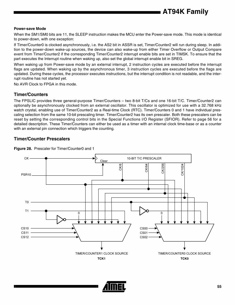
AT94K Family
Power-save Mode
When the SM1/SM0 bits are 11, the SLEEP instruction makes the MCU enter the Power-save mode. This mode is identicalto power-down, with one exception:
If Timer/Counter0 is clocked asynchronously, i.e. the AS2 bit in ASSR is set, Timer/Counter2 will run during sleep. In addi-tion to the power-down wake-up sources, the device can also wake-up from either Timer Overflow or Output Compareevent from Timer/Counter2 if the corresponding Timer/Counter2 interrupt enable bits are set in TIMSK. To ensure that thepart executes the Interrupt routine when waking up, also set the global interrupt enable bit in SREG.
When waking up from Power-save mode by an external interrupt, 2 instruction cycles are executed before the interruptflags are updated. When waking up by the asynchronous timer, 3 instruction cycles are executed before the flags areupdated. During these cycles, the processor executes instructions, but the interrupt condition is not readable, and the inter-rupt routine has not started yet.
No AVR Clock to FPGA in this mode.
Timer/CountersThe FPSLIC provides three general-purpose Timer/Counters – two 8-bit T/Cs and one 16-bit T/C. Timer/Counter2 canoptionally be asynchronously clocked from an external oscillator. This oscillator is optimized for use with a 32.768 kHzwatch crystal, enabling use of Timer/Counter2 as a Real-time Clock (RTC). Timer/Counters 0 and 1 have individual pres-caling selection from the same 10-bit prescaling timer. Timer/Counter2 has its own prescaler. Both these prescalers can bereset by setting the corresponding control bits in the Special Functions I/O Register (SFIOR). Refer to page 56 for adetailed description. These Timer/Counters can either be used as a timer with an internal clock time-base or as a counterwith an external pin connection which triggers the counting.
Timer/Counter Prescalers
Figure 28. Prescaler for Timer/Counter0 and 1
PSR10
Clear
TCK1 TCK0
55
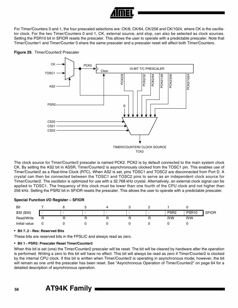
For Timer/Counters 0 and 1, the four prescaled selections are: CK/8, CK/64, CK/256 and CK/1024, where CK is the oscilla-tor clock. For the two Timer/Counters 0 and 1, CK, external source, and stop, can also be selected as clock sources.Setting the PSR10 bit in SFIOR resets the prescaler. This allows the user to operate with a predictable prescaler. Note thatTimer/Counter1 and Timer/Counter 0 share the same prescaler and a prescaler reset will affect both Timer/Counters.
Figure 29. Timer/Counter2 Prescaler
The clock source for Timer/Counter2 prescaler is named PCK2. PCK2 is by default connected to the main system clockCK. By setting the AS2 bit in ASSR, Timer/Counter2 is asynchronously clocked from the TOSC1 pin. This enables use ofTimer/Counter2 as a Real-time Clock (RTC). When AS2 is set, pins TOSC1 and TOSC2 are disconnected from Port D. Acrystal can then be connected between the TOSC1 and TOSC2 pins to serve as an independent clock source forTimer/Counter2. The oscillator is optimized for use with a 32.768 kHz crystal. Alternatively, an external clock signal can beapplied to TOSC1. The frequency of this clock must be lower than one fourth of the CPU clock and not higher than256 kHz. Setting the PSR2 bit in SFIOR resets the prescaler. This allows the user to operate with a predictable prescaler.
Special Function I/O Register – SFIOR
• Bit 7..2 - Res: Reserved Bits
These bits are reserved bits in the FPSLIC and always read as zero.
• Bit 1 - PSR2: Prescaler Reset Timer/Counter2
When this bit is set (one) the Timer/Counter2 prescaler will be reset. The bit will be cleared by hardware after the operationis performed. Writing a zero to this bit will have no effect. This bit will always be read as zero if Timer/Counter2 is clockedby the internal CPU clock. If this bit is written when Timer/Counter2 is operating in asynchronous mode; however, the bitwill remain as one until the prescaler has been reset. See “Asynchronous Operation of Timer/Counter2” on page 64 for adetailed description of asynchronous operation.
Bit 7 6 5 4 3 2 1 0
$30 ($50) - - - - - - PSR2 PSR10 SFIOR
Read/Write R R R R R R R/W R/W
Initial value 0 0 0 0 0 0 0 0
10-BIT T/C PRESCALER
TIMER/COUNTER2 CLOCK SOURCE
CK PCK2
TOSC1
AS2
CS20CS21CS22
PC
K2/
8
PC
K2/
64
PC
K2/
128
PC
K2/
1024
PC
K2/
256
PC
K2/
32
0PSR2
Clear
TCK2
AT94K Family56
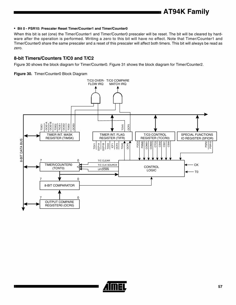
AT94K Family
• Bit 0 - PSR10: Prescaler Reset Timer/Counter1 and Timer/Counter0
When this bit is set (one) the Timer/Counter1 and Timer/Counter0 prescaler will be reset. The bit will be cleared by hard-ware after the operation is performed. Writing a zero to this bit will have no effect. Note that Timer/Counter1 andTimer/Counter0 share the same prescaler and a reset of this prescaler will affect both timers. This bit will always be read aszero.
8-bit Timers/Counters T/C0 and T/C2Figure 30 shows the block diagram for Timer/Counter0. Figure 31 shows the block diagram for Timer/Counter2.
Figure 30. Timer/Counter0 Block Diagram
8-B
IT D
ATA
BU
S
TIMER INT. FLAGREGISTER (TIFR)
TIMER/COUNTER0(TCNT0)
8-BIT COMPARATOR
OUTPUT COMPAREREGISTER0 (OCR0)
TIMER INT. MASKREGISTER (TIMSK)
0
0
0
7
7
7
T/C CLK SOURCE
UP/DOWN
T/C CLEAR
CONTROLLOGIC
TO
V1
OC
F1B
OC
F1A
ICF
1
TO
V2
OC
F2
OC
F0
TO
V0
CK
T/C0 OVER-FLOW IRQ
T/C0 COMPAREMATCH IRQ
OC
F0
TO
V0
TO
IE0
TO
IE1
OC
IE1A
OC
IE1B
TIC
IE1
TO
IE2
OC
IE2
OC
IE0
T/C0 CONTROLREGISTER (TCCR0)
CS
02
CO
M01
PW
M0
CS
01
CO
M00
CS
00
CT
C0
FO
C0
PS
R2
PS
R10
SPECIAL FUNCTIONSIO REGISTER (SFIOR)
T0
57

Figure 31. Timer/Counter2 Block Diagram
The 8-bit Timer/Counter0 can select clock source from CK, prescaled CK, or an external pin.
The 8-bit Timer/Counter2 can select clock source from CK, prescaled CK or external TOSC1.
Both Timers/Counters can be stopped as described in section “Timer/Counter0 Control Register – TCCR0” on page 59 and“Timer/Counter2 Control Register – TCCR2” on page 59
The various status flags (overflow and compare match) are found in the Timer/Counter Interrupt Flag Register – TIFR. Con-trol signals are found in the Timer/Counter Control Register – TCCR0 and TCCR2. The interrupt enable/disable settingsare found in the Timer/Counter Interrupt Mask Register – TIMSK.
When Timer/Counter0 is externally clocked, the external signal is synchronized with the oscillator frequency of the CPU. Toassure proper sampling of the external clock, the minimum time between two external clock transitions must be at least oneinternal CPU clock period. The external clock signal is sampled on the rising edge of the internal CPU clock.
The 8-bit Timer/Counters feature both a high-resolution and a high-accuracy usage with the lower prescaling opportunities.Similarly, the high prescaling opportunities make the Timer/Counter0 useful for lower speed functions or exact-timing func-tions with infrequent actions.
Timer/Counter0 and 2 can also be used as 8-bit Pulse-width Modulators. In this mode, the Timer/Counter and the outputcompare register serve as a glitch-free, stand-alone PWM with centered pulses. Refer to page 61 for a detailed descriptionon this function.
8-BIT DATA BUS
8-BIT ASYNCH T/C2 DATA BUS
ASYNCH. STATUSREGISTER (ASSR)
TIMER INT. FLAGREGISTER (TIFR)
TIMER/COUNTER2(TCNT2)
SYNCH UNIT
8-BIT COMPARATOR
OUTPUT COMPAREREGISTER2 (OCR2)
TIMER INT. MASKREGISTER (TIMSK)
0
0
0
7
7
7
T/C CLK SOURCE
UP/DOWN
T/C CLEAR
CONTROLLOGIC
OC
F2
TO
V2
TO
IE0
TO
IE1
OC
IE1A
OC
IE1B
TIC
IE1
TO
IE2
OC
IE2
OC
R2U
B
TC
2UB
ICR
2UB
TOSC1
CKTCK2
T/C2 OVER-FLOW IRQ
T/C2 COMPAREMATCH IRQ
AS
2
TO
V1
OC
F1B
OC
F1A
ICF
1
TO
V2
OC
F2
OC
F0
TO
V0
OC
IE0
T/C2 CONTROLREGISTER (TCCR2)
CS
22
CO
M21
PW
M2
CS
21
CO
M20
CS
20
CT
C2
FO
C2
PS
R2
PS
R10
SPECIAL FUNCTIONSIO REGISTER (SFIOR)
CK
AT94K Family58
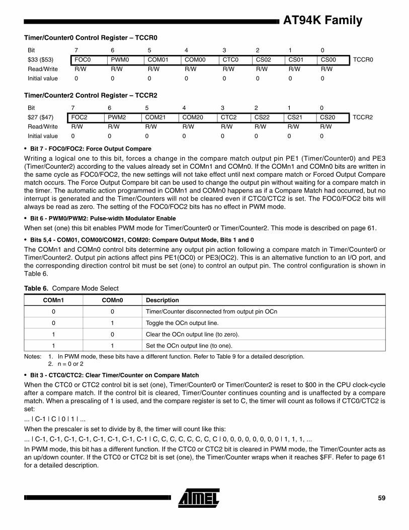
AT94K Family
Timer/Counter0 Control Register – TCCR0Timer/Counter2 Control Register – TCCR2
• Bit 7 - FOC0/FOC2: Force Output Compare
Writing a logical one to this bit, forces a change in the compare match output pin PE1 (Timer/Counter0) and PE3(Timer/Counter2) according to the values already set in COMn1 and COMn0. If the COMn1 and COMn0 bits are written inthe same cycle as FOC0/FOC2, the new settings will not take effect until next compare match or Forced Output Comparematch occurs. The Force Output Compare bit can be used to change the output pin without waiting for a compare match inthe timer. The automatic action programmed in COMn1 and COMn0 happens as if a Compare Match had occurred, but nointerrupt is generated and the Timer/Counters will not be cleared even if CTC0/CTC2 is set. The FOC0/FOC2 bits willalways be read as zero. The setting of the FOC0/FOC2 bits has no effect in PWM mode.
• Bit 6 - PWM0/PWM2: Pulse-width Modulator Enable
When set (one) this bit enables PWM mode for Timer/Counter0 or Timer/Counter2. This mode is described on page 61.
• Bits 5,4 - COM01, COM00/COM21, COM20: Compare Output Mode, Bits 1 and 0
The COMn1 and COMn0 control bits determine any output pin action following a compare match in Timer/Counter0 orTimer/Counter2. Output pin actions affect pins PE1(OC0) or PE3(OC2). This is an alternative function to an I/O port, andthe corresponding direction control bit must be set (one) to control an output pin. The control configuration is shown inTable 6.
Notes: 1. In PWM mode, these bits have a different function. Refer to Table 9 for a detailed description.2. n = 0 or 2
• Bit 3 - CTC0/CTC2: Clear Timer/Counter on Compare Match
When the CTC0 or CTC2 control bit is set (one), Timer/Counter0 or Timer/Counter2 is reset to $00 in the CPU clock-cycleafter a compare match. If the control bit is cleared, Timer/Counter continues counting and is unaffected by a comparematch. When a prescaling of 1 is used, and the compare register is set to C, the timer will count as follows if CTC0/CTC2 isset:
... | C-1 | C | 0 | 1 | ...
When the prescaler is set to divide by 8, the timer will count like this:
... | C-1, C-1, C-1, C-1, C-1, C-1, C-1, C-1 | C, C, C, C, C, C, C, C | 0, 0, 0, 0, 0, 0, 0, 0 | 1, 1, 1, ...
In PWM mode, this bit has a different function. If the CTC0 or CTC2 bit is cleared in PWM mode, the Timer/Counter acts asan up/down counter. If the CTC0 or CTC2 bit is set (one), the Timer/Counter wraps when it reaches $FF. Refer to page 61for a detailed description.
Bit 7 6 5 4 3 2 1 0
$33 ($53) FOC0 PWM0 COM01 COM00 CTC0 CS02 CS01 CS00 TCCR0
Read/Write R/W R/W R/W R/W R/W R/W R/W R/W
Initial value 0 0 0 0 0 0 0 0
Bit 7 6 5 4 3 2 1 0
$27 ($47) FOC2 PWM2 COM21 COM20 CTC2 CS22 CS21 CS20 TCCR2
Read/Write R/W R/W R/W R/W R/W R/W R/W R/W
Initial value 0 0 0 0 0 0 0 0
Table 6. Compare Mode Select
COMn1 COMn0 Description
0 0 Timer/Counter disconnected from output pin OCn
0 1 Toggle the OCn output line.
1 0 Clear the OCn output line (to zero).
1 1 Set the OCn output line (to one).
59

• Bits 2,1,0 - CS02, CS01, CS00/ CS22, CS21, CS20: Clock Select Bits 2,1 and 0
The Clock Select bits 2,1 and 0 define the prescaling source of Timer/Counter0 and Timer/Counter2.
The Stop condition provides a Timer Enable/Disable function. The prescaled modes are scaled directly from the CK oscilla-tor clock for Timer/Counter0 and PCK2 for Timer/Counter2. If the external pin modes are used for Timer/Counter0,transitions on PE0/(T0) will clock the counter even if the pin is configured as an output. This feature can give the user SWcontrol of the counting.
Timer Counter0 – TCNT0
Timer/Counter2 – TCNT2
These 8-bit registers contain the value of the Timer/Counters.
Table 7. Clock 0 Prescale Select
CS02 CS01 CS00 Description
0 0 0 Stop, the Timer/Counter0 is stopped.
0 0 1 CK
0 1 0 CK/8
0 1 1 CK/64
1 0 0 CK/256
1 0 1 CK/1024
1 1 0 External Pin PB0(T0), falling edge
1 1 1 External Pin PB0(T0), rising edge
Table 8. Clock 2 Prescale Select
CS22 CS21 CS20 Description
0 0 0 Stop, the Timer/Counter2 is stopped.
0 0 1 PCK2
0 1 0 PCK2/8
0 1 1 PCK2/32
1 0 0 PCK2/64
1 0 1 PCK2/128
1 1 0 PCK2/256
1 1 1 PCK2/1024
Bit 7 6 5 4 3 2 1 0
$32 ($52) MSB LSB TCNT0
Read/Write R/W R/W R/W R/W R/W R/W R/W R/W
Initial value 0 0 0 0 0 0 0 0
Bit 7 6 5 4 3 2 1 0
$23 ($43) MSB LSB TCNT2
Read/Write R/W R/W R/W R/W R/W R/W R/W R/W
Initial value 0 0 0 0 0 0 0 0
AT94K Family60
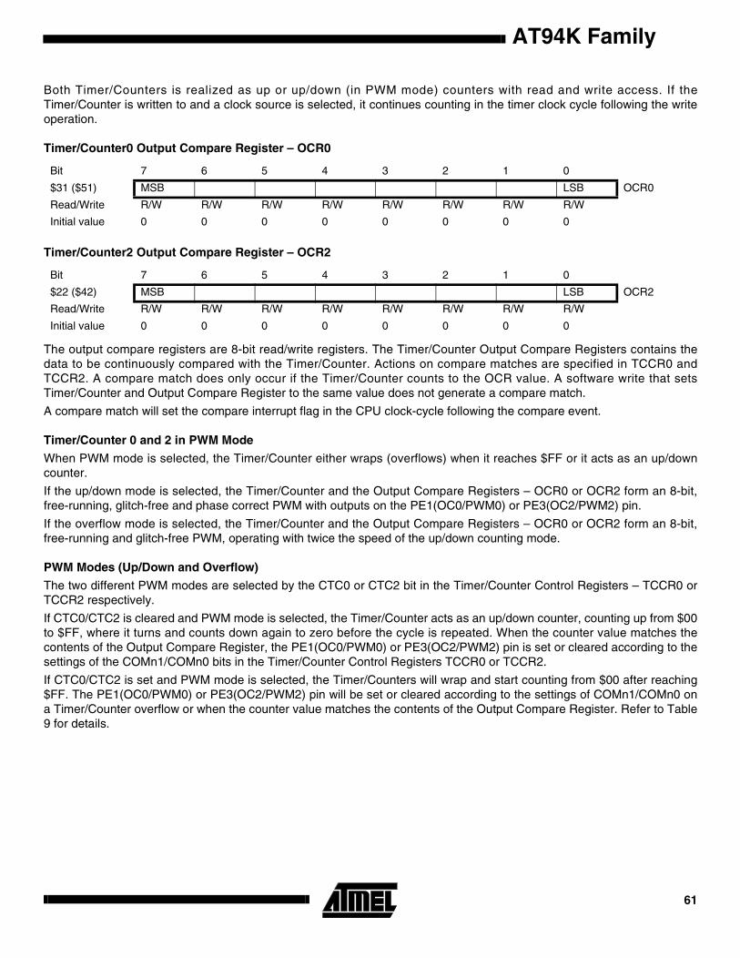
AT94K Family
Both Timer/Counters is realized as up or up/down (in PWM mode) counters with read and write access. If theTimer/Counter is written to and a clock source is selected, it continues counting in the timer clock cycle following the writeoperation.
Timer/Counter0 Output Compare Register – OCR0
Timer/Counter2 Output Compare Register – OCR2
The output compare registers are 8-bit read/write registers. The Timer/Counter Output Compare Registers contains thedata to be continuously compared with the Timer/Counter. Actions on compare matches are specified in TCCR0 andTCCR2. A compare match does only occur if the Timer/Counter counts to the OCR value. A software write that setsTimer/Counter and Output Compare Register to the same value does not generate a compare match.
A compare match will set the compare interrupt flag in the CPU clock-cycle following the compare event.
Timer/Counter 0 and 2 in PWM Mode
When PWM mode is selected, the Timer/Counter either wraps (overflows) when it reaches $FF or it acts as an up/downcounter.
If the up/down mode is selected, the Timer/Counter and the Output Compare Registers – OCR0 or OCR2 form an 8-bit,free-running, glitch-free and phase correct PWM with outputs on the PE1(OC0/PWM0) or PE3(OC2/PWM2) pin.
If the overflow mode is selected, the Timer/Counter and the Output Compare Registers – OCR0 or OCR2 form an 8-bit,free-running and glitch-free PWM, operating with twice the speed of the up/down counting mode.
PWM Modes (Up/Down and Overflow)
The two different PWM modes are selected by the CTC0 or CTC2 bit in the Timer/Counter Control Registers – TCCR0 orTCCR2 respectively.
If CTC0/CTC2 is cleared and PWM mode is selected, the Timer/Counter acts as an up/down counter, counting up from $00to $FF, where it turns and counts down again to zero before the cycle is repeated. When the counter value matches thecontents of the Output Compare Register, the PE1(OC0/PWM0) or PE3(OC2/PWM2) pin is set or cleared according to thesettings of the COMn1/COMn0 bits in the Timer/Counter Control Registers TCCR0 or TCCR2.
If CTC0/CTC2 is set and PWM mode is selected, the Timer/Counters will wrap and start counting from $00 after reaching$FF. The PE1(OC0/PWM0) or PE3(OC2/PWM2) pin will be set or cleared according to the settings of COMn1/COMn0 ona Timer/Counter overflow or when the counter value matches the contents of the Output Compare Register. Refer to Table9 for details.
Bit 7 6 5 4 3 2 1 0
$31 ($51) MSB LSB OCR0
Read/Write R/W R/W R/W R/W R/W R/W R/W R/W
Initial value 0 0 0 0 0 0 0 0
Bit 7 6 5 4 3 2 1 0
$22 ($42) MSB LSB OCR2
Read/Write R/W R/W R/W R/W R/W R/W R/W R/W
Initial value 0 0 0 0 0 0 0 0
61
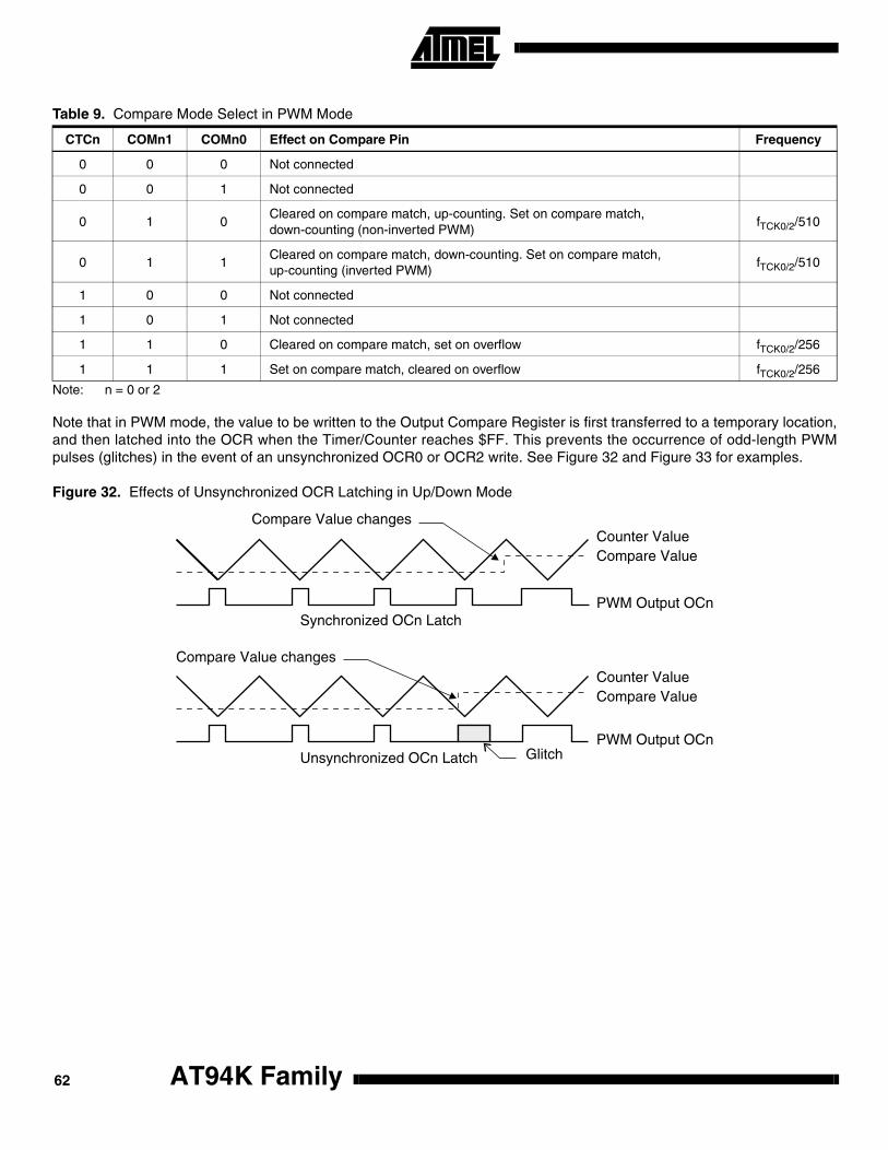
Note: n = 0 or 2
Note that in PWM mode, the value to be written to the Output Compare Register is first transferred to a temporary location,and then latched into the OCR when the Timer/Counter reaches $FF. This prevents the occurrence of odd-length PWMpulses (glitches) in the event of an unsynchronized OCR0 or OCR2 write. See Figure 32 and Figure 33 for examples.
Figure 32. Effects of Unsynchronized OCR Latching in Up/Down Mode
Table 9. Compare Mode Select in PWM Mode
CTCn COMn1 COMn0 Effect on Compare Pin Frequency
0 0 0 Not connected
0 0 1 Not connected
0 1 0Cleared on compare match, up-counting. Set on compare match, down-counting (non-inverted PWM)
fTCK0/2/510
0 1 1Cleared on compare match, down-counting. Set on compare match, up-counting (inverted PWM)
fTCK0/2/510
1 0 0 Not connected
1 0 1 Not connected
1 1 0 Cleared on compare match, set on overflow fTCK0/2/256
1 1 1 Set on compare match, cleared on overflow fTCK0/2/256
PWM Output OCn
PWM Output OCnUnsynchronized OCn Latch
Synchronized OCn Latch
Compare Value changesCounter ValueCompare Value
Glitch
Counter ValueCompare Value
Compare Value changes
AT94K Family62
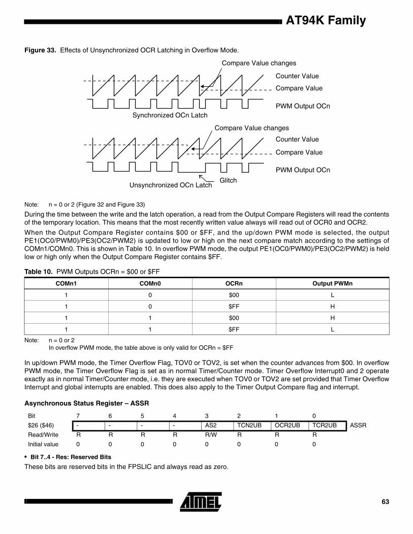
AT94K Family
Figure 33. Effects of Unsynchronized OCR Latching in Overflow Mode.
Note: n = 0 or 2 (Figure 32 and Figure 33)
During the time between the write and the latch operation, a read from the Output Compare Registers will read the contentsof the temporary location. This means that the most recently written value always will read out of OCR0 and OCR2.
When the Output Compare Register contains $00 or $FF, and the up/down PWM mode is selected, the outputPE1(OC0/PWM0)/PE3(OC2/PWM2) is updated to low or high on the next compare match according to the settings ofCOMn1/COMn0. This is shown in Table 10. In overflow PWM mode, the output PE1(OC0/PWM0)/PE3(OC2/PWM2) is heldlow or high only when the Output Compare Register contains $FF.
Note: n = 0 or 2In overflow PWM mode, the table above is only valid for OCRn = $FF
In up/down PWM mode, the Timer Overflow Flag, TOV0 or TOV2, is set when the counter advances from $00. In overflowPWM mode, the Timer Overflow Flag is set as in normal Timer/Counter mode. Timer Overflow Interrupt0 and 2 operateexactly as in normal Timer/Counter mode, i.e. they are executed when TOV0 or TOV2 are set provided that Timer OverflowInterrupt and global interrupts are enabled. This does also apply to the Timer Output Compare flag and interrupt.
Asynchronous Status Register – ASSR
• Bit 7..4 - Res: Reserved Bits
These bits are reserved bits in the FPSLIC and always read as zero.
Table 10. PWM Outputs OCRn = $00 or $FF
COMn1 COMn0 OCRn Output PWMn
1 0 $00 L
1 0 $FF H
1 1 $00 H
1 1 $FF L
Bit 7 6 5 4 3 2 1 0
$26 ($46) - - - - AS2 TCN2UB OCR2UB TCR2UB ASSR
Read/Write R R R R R/W R R R
Initial value 0 0 0 0 0 0 0 0
PWM Output OCn
PWM Output OCn
Unsynchronized OCn Latch
Synchronized OCn Latch
Counter Value
Compare Value
Counter Value
Compare Value
Compare Value changes
Compare Value changes
Glitch
63
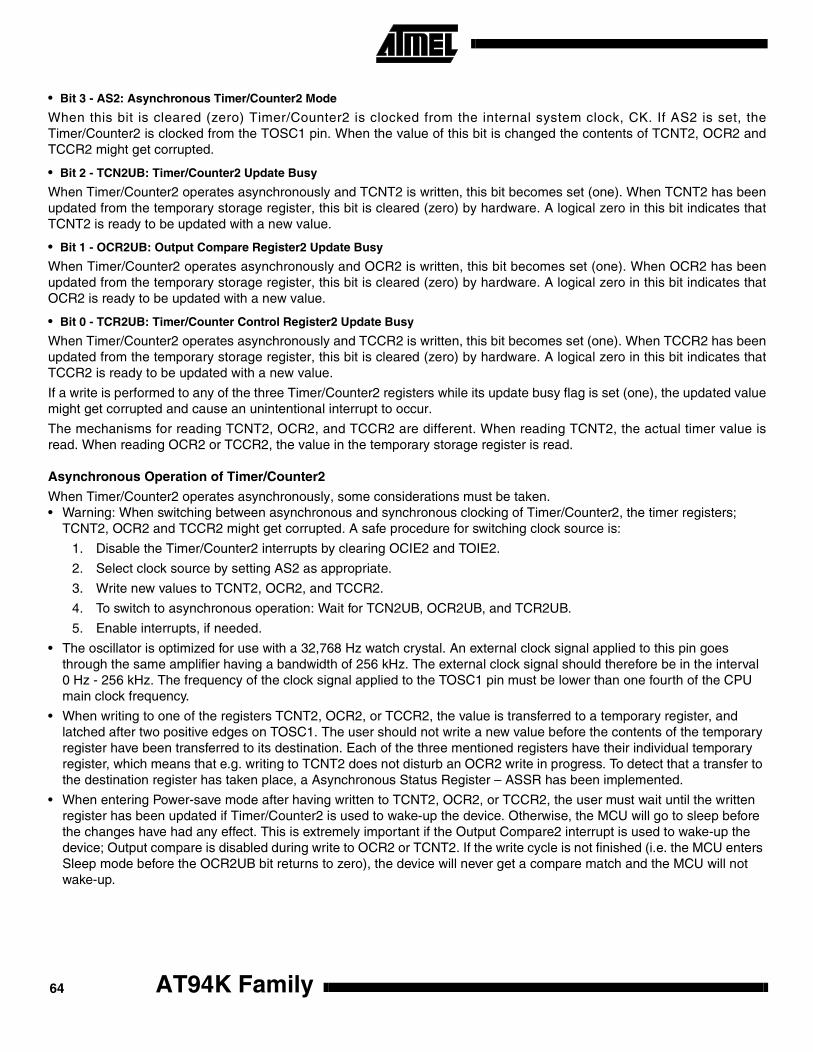
• Bit 3 - AS2: Asynchronous Timer/Counter2 Mode
When this bit is cleared (zero) Timer/Counter2 is clocked from the internal system clock, CK. If AS2 is set, theTimer/Counter2 is clocked from the TOSC1 pin. When the value of this bit is changed the contents of TCNT2, OCR2 andTCCR2 might get corrupted.
• Bit 2 - TCN2UB: Timer/Counter2 Update Busy
When Timer/Counter2 operates asynchronously and TCNT2 is written, this bit becomes set (one). When TCNT2 has beenupdated from the temporary storage register, this bit is cleared (zero) by hardware. A logical zero in this bit indicates thatTCNT2 is ready to be updated with a new value.
• Bit 1 - OCR2UB: Output Compare Register2 Update Busy
When Timer/Counter2 operates asynchronously and OCR2 is written, this bit becomes set (one). When OCR2 has beenupdated from the temporary storage register, this bit is cleared (zero) by hardware. A logical zero in this bit indicates thatOCR2 is ready to be updated with a new value.
• Bit 0 - TCR2UB: Timer/Counter Control Register2 Update Busy
When Timer/Counter2 operates asynchronously and TCCR2 is written, this bit becomes set (one). When TCCR2 has beenupdated from the temporary storage register, this bit is cleared (zero) by hardware. A logical zero in this bit indicates thatTCCR2 is ready to be updated with a new value.
If a write is performed to any of the three Timer/Counter2 registers while its update busy flag is set (one), the updated valuemight get corrupted and cause an unintentional interrupt to occur.
The mechanisms for reading TCNT2, OCR2, and TCCR2 are different. When reading TCNT2, the actual timer value isread. When reading OCR2 or TCCR2, the value in the temporary storage register is read.
Asynchronous Operation of Timer/Counter2
When Timer/Counter2 operates asynchronously, some considerations must be taken.• Warning: When switching between asynchronous and synchronous clocking of Timer/Counter2, the timer registers;
TCNT2, OCR2 and TCCR2 might get corrupted. A safe procedure for switching clock source is:
1. Disable the Timer/Counter2 interrupts by clearing OCIE2 and TOIE2.
2. Select clock source by setting AS2 as appropriate.
3. Write new values to TCNT2, OCR2, and TCCR2.
4. To switch to asynchronous operation: Wait for TCN2UB, OCR2UB, and TCR2UB.
5. Enable interrupts, if needed.
• The oscillator is optimized for use with a 32,768 Hz watch crystal. An external clock signal applied to this pin goes through the same amplifier having a bandwidth of 256 kHz. The external clock signal should therefore be in the interval 0 Hz - 256 kHz. The frequency of the clock signal applied to the TOSC1 pin must be lower than one fourth of the CPU main clock frequency.
• When writing to one of the registers TCNT2, OCR2, or TCCR2, the value is transferred to a temporary register, and latched after two positive edges on TOSC1. The user should not write a new value before the contents of the temporary register have been transferred to its destination. Each of the three mentioned registers have their individual temporary register, which means that e.g. writing to TCNT2 does not disturb an OCR2 write in progress. To detect that a transfer to the destination register has taken place, a Asynchronous Status Register – ASSR has been implemented.
• When entering Power-save mode after having written to TCNT2, OCR2, or TCCR2, the user must wait until the written register has been updated if Timer/Counter2 is used to wake-up the device. Otherwise, the MCU will go to sleep before the changes have had any effect. This is extremely important if the Output Compare2 interrupt is used to wake-up the device; Output compare is disabled during write to OCR2 or TCNT2. If the write cycle is not finished (i.e. the MCU enters Sleep mode before the OCR2UB bit returns to zero), the device will never get a compare match and the MCU will not wake-up.
AT94K Family64
AT94K Family
• If Timer/Counter2 is used to wake-up the device from Power-save mode, precautions must be taken if the user wants to re-enter Power-save mode: The interrupt logic needs one TOSC1 cycle to be reset. If the time between wake-up and reentering Power-save mode is less than one TOSC1 cycle, the interrupt will not occur and the device will fail to wakeup. If the user is in doubt whether the time before re-entering power-save is sufficient, the following algorithm can be used to ensure that one TOSC1 cycle has elapsed:
1. Write a value to TCCR2, TCNT2, or OCR2
2. Wait until the corresponding Update Busy flag in ASSR returns to zero.
3. Enter Power-save mode
• When asynchronous operation is selected, the 32 kHz oscillator for Timer/Counter2 is always running, except in Power-down mode. After a power-up reset or wake-up from power-down, the user should be aware of the fact that this oscillator might take as long as one second to stabilize. Therefore, the contents of all Timer2 registers must be considered lost after a wake-up from power-down, due to the unstable clock signal. The user is advised to wait for at least one second before using Timer/Counter2 after power-up or wake-up from power-down.
• Description of wake-up from Power-save mode when the timer is clocked asynchronously: When the interrupt condition is met, the wake-up process is started on the following cycle of the timer clock, that is, the timer is always advanced by at least one before the processor can read the counter value. The interrupt flags are updated 3 processor cycles after the processor clock has started. During these cycles, the processor executes instructions, but the interrupt condition is not readable, and the interrupt routine has not started yet.
• During asynchronous operation, the synchronization of the interrupt flags for the asynchronous timer takes 3 processor cycles plus one timer cycle. The timer is therefore advanced by at least one before the processor can read the timer value causing the setting of the interrupt flag. The output compare pin is changed on the timer clock and is not synchronized to the processor clock.
65

Timer/Counter1Figure 34 shows the block diagram for Timer/Counter1.
Figure 34. Timer/Counter1 Block Diagram
The 16-bit Timer/Counter1 can select clock source from CK, prescaled CK, or an external pin. In addition it can be stoppedas described in section “Timer/Counter1 Control Register B – TCCR1B” on page 68. The different status flags (overflow,compare match and capture event) are found in the Timer/Counter Interrupt Flag Register – TIFR. Control signals arefound in the Timer/Counter1 Control Registers – TCCR1A and TCCR1B. The interrupt enable/disable settings forTimer/Counter1 are found in the Timer/Counter Interrupt Mask Register – TIMSK.
When Timer/Counter1 is externally clocked, the external signal is synchronized with the oscillator frequency of the CPU. Toassure proper sampling of the external clock, the minimum time between two external clock transitions must be at least oneinternal CPU clock period. The external clock signal is sampled on the rising edge of the internal CPU clock.
The 16-bit Timer/Counter1 features both a high-resolution and a high-accuracy usage with the lower prescaling opportuni-ties. Similarly, the high-prescaling opportunities makes the Timer/Counter1 useful for lower speed functions or exact-timingfunctions with infrequent actions.
The Timer/Counter1 supports two Output Compare functions using the Output Compare Register 1 A and B – OCR1A andOCR1B as the data sources to be compared to the Timer/Counter1 contents. The Output Compare functions includeoptional clearing of the counter on compareA match, and actions on the Output Compare pins on both compare matches.
TO
IE0
TO
IE1
OC
IE1A
OC
IE1B
TIC
IE1
TO
IE2
OC
IE2
OC
IE0
TO
V0
TO
V1
OC
F1A
OC
F1B
ICF
1
TO
V2
OC
F2
OC
F0
TIMER INT. FLAGREGISTER (TIFR)
CONTROLLOGIC
TIMER/COUNTER1 (TCNT1)
TIMER INT. MASKREGISTER (TIMSK)
T/C1 INPUT CAPTURE REGISTER (ICR1)
T/C1 OVER-FLOW IRQ
T/C1 COMPAREMATCHA IRQ
T/C1 COMPAREMATCHB IRQ
T/C1 INPUTCAPTURE IRQ
8-B
IT D
AT
A B
US
16 BIT COMPARATOR
TIMER/COUNTER1 OUTPUT COMPARE REGISTER A
16 BIT COMPARATOR
TIMER/COUNTER1 OUTPUT COMPARE REGISTER B
CAPTURETRIGGER
CK
07815
07815
07815
07815 07815
07815
T/C CLEAR
T/C CLOCK SOURCE
UP/DOWN
T/C1 CONTROLREGISTER A (TCCR1A)
T/C1 CONTROLREGISTER B (TCCR1B)
FO
C1A
FO
C1B
CO
M1A
1
CO
M1A
0
CO
M1B
1
CO
M1B
0
PW
M11
PW
M10
ICN
C1
ICE
S1
CT
C1
CS
12
CS
11
CS
10
PS
R2
PS
R10
SPECIAL FUNCTIONSIO REGISTER (SFIOR)
TO
V1
OC
F1B
OC
F1A
ICF
1
TO
V2
OC
F2
OC
F0
TO
V0
T1
AT94K Family66
AT94K Family
Timer/Counter1 can also be used as a 8-, 9- or 10-bit Pulse-with Modulator. In this mode the counter and theOCR1A/OCR1B registers serve as a dual-glitch-free stand-alone PWM with centered pulses. Alternatively, theTimer/Counter1 can be configured to operate at twice the speed in PWM mode, but without centered pulses. Refer topage 71 for a detailed description on this function.
The Input Capture function of Timer/Counter1 provides a capture of the Timer/Counter1 contents to the Input CaptureRegister – ICR1, triggered by an external event on the Input Capture Pin – PE7(ICP). The actual capture event settings aredefined by the Timer/Counter1 Control Register – TCCR1B.
Figure 35. ICP Pin Schematic Diagram
If the noise canceler function is enabled, the actual trigger condition for the capture event is monitored over 4 samples, andall 4 must be equal to activate the capture flag.
Timer/Counter1 Control Register A – TCCR1A
• Bits 7,6 - COM1A1, COM1A0: Compare Output Mode1A, Bits 1 and 0
The COM1A1 and COM1A0 control bits determine any output pin action following a compare match in Timer/Counter1.Any output pin actions affect pin OC1A – Output CompareA pin PE6. This is an alternative function to an I/O port, and thecorresponding direction control bit must be set (one) to control an output pin. The control configuration is shown in Table11.
• Bits 5,4 - COM1B1, COM1B0: Compare Output Mode1B, Bits 1 and 0
The COM1B1 and COM1B0 control bits determine any output pin action following a compare match in Timer/Counter1.Any output pin actions affect pin OC1B – Output CompareB pin PE5. This is an alternative function to an I/O port, and thecorresponding direction control bit must be set (one) to control an output pin. The following control configuration is given:
Note: X = A or BIn PWM mode, these bits have a different function. Refer to Table 15 for a detailed description.
Bit 7 6 5 4 3 2 1 0
$2F ($4F) COM1A1 COM1A0 COM1B1 COM1B0 FOC1A FOC1B PWM11 PWM10 TCCR1A
Read/Write R/W R/W R/W R/W R/w R/W R/W R/W
Initial value 0 0 0 0 0 0 0 0
Table 11. Compare 1 Mode Select
COM1X1 COM1X0 Description
0 0 Timer/Counter1 disconnected from output pin OC1X
0 1 Toggle the OC1X output line.
1 0 Clear the OC1X output line (to zero).
1 1 Set the OC1X output line (to one).
ICPE
ICPE: Input Capture Pin Enable
67

• Bit 3 - FOC1A: Force Output Compare1A
Writing a logical one to this bit, forces a change in the compare match output pin PE6 according to the values already set inCOM1A1 and COM1A0. If the COM1A1 and COM1A0 bits are written in the same cycle as FOC1A, the new settings willnot take effect until next compare match or forced compare match occurs. The Force Output Compare bit can be used tochange the output pin without waiting for a compare match in the timer. The automatic action programmed in COM1A1 andCOM1A0 happens as if a Compare Match had occurred, but no interrupt is generated and it will not clear the timer even ifCTC1 in TCCR1B is set. The FOC1A bit will always be read as zero. The setting of the FOC1A bit has no effect in PWMmode.
• Bit 2 - FOC1B: Force Output Compare1B
Writing a logical one to this bit, forces a change in the compare match output pin PE5 according to the values already set inCOM1B1 and COM1B0. If the COM1B1 and COM1B0 bits are written in the same cycle as FOC1B, the new settings willnot take effect until next compare match or forced compare match occurs. The Force Output Compare bit can be used tochange the output pin without waiting for a compare match in the timer. The automatic action programmed in COM1B1 andCOM1B0 happens as if a Compare Match had occurred, but no interrupt is generated. The FOC1B bit will always be readas zero. The setting of the FOC1B bit has no effect in PWM mode.
• Bits 1..0 - PWM11, PWM10: Pulse-width Modulator Select Bits
These bits select PWM operation of Timer/Counter1 as specified in Table 12. This mode is described on page 71.
Timer/Counter1 Control Register B – TCCR1B
• Bit 7 - ICNC1: Input Capture1 Noise Canceler (4 CKs)
When the ICNC1 bit is cleared (zero), the input capture trigger noise canceler function is disabled. The input capture is trig-gered at the first rising/falling edge sampled on the PE7(ICP) – input capture pin – as specified. When the ICNC1 bit is set(one), four successive samples are measures on the PE7(ICP) – input capture pin, and all samples must be high/lowaccording to the input capture trigger specification in the ICES1 bit. The actual sampling frequency is XTAL clockfrequency.
• Bit 6 - ICES1: Input Capture1 Edge Select
While the ICES1 bit is cleared (zero), the Timer/Counter1 contents are transferred to the Input Capture Register – ICR1 –on the falling edge of the input capture pin – PE7(ICP). While the ICES1 bit is set (one), the Timer/Counter1 contents aretransferred to the Input Capture Register – ICR1 – on the rising edge of the input capture pin – PE7(ICP).
• Bit 5 - ICPE: Input Captive Pin Enable
This bit must be set by the user to enable the Input Capture Function of timer1. Disabling prevents necessary registercopies during normal use of the PE7 port.
• Bit 4 - Res: Reserved Bit
This bit is reserved in the FPSLIC and will always read zero.
Table 12. PWM Mode Select
PWM11 PWM10 Description
0 0 PWM operation of Timer/Counter1 is disabled
0 1 Timer/Counter1 is an 8-bit PWM
1 0 Timer/Counter1 is a 9-bit PWM
1 1 Timer/Counter1 is a 10-bit PWM
Bit 7 6 5 4 3 2 1 0
$2E ($4E) ICNC1 ICES1 ICPE - CTC1 CS12 CS11 CS10 TCCR1B
Read/Write R/W R/W R/W R R/W R/W R/W R/W
Initial value 0 0 0 0 0 0 0 0
AT94K Family68
AT94K Family
• Bit 3 - CTC1: Clear Timer/Counter1 on Compare Match
When the CTC1 control bit is set (one), the Timer/Counter1 is reset to $0000 in the clock cycle after a compareA match. Ifthe CTC1 control bit is cleared, Timer/Counter1 continues counting and is unaffected by a compare match. When a pres-caling of 1 is used, and the compareA register is set to C, the timer will count as follows if CTC1 is set:
... | C-1 | C | 0 | 1 | ...
When the prescaler is set to divide by 8, the timer will count like this:
... | C-1, C-1, C-1, C-1, C-1, C-1, C-1, C-1 | C, C, C, C, C, C, C, C | 0, 0, 0, 0, 0, 0, 0, 0 | ...
In PWM mode, this bit has a different function. If the CTC1 bit is cleared in PWM mode, the Timer/Counter1 acts as anup/down counter. If the CTC1 bit is set (one), the Timer/Counter wraps when it reaches the TOP value. Refer to page 71 fora detailed description.
• Bits 2,1,0 - CS12, CS11, CS10: Clock Select1, bit 2,1 and 0
The Clock Select1 bits 2,1 and 0 define the prescaling source of Timer/Counter1.
The Stop condition provides a Timer Enable/Disable function. The CK down-divided modes are scaled directly from the CKoscillator clock. If the external pin modes are used for Timer/Counter1, transitions on PE4/(T1) will clock the counter even ifthe pin is configured as an output. This feature can give the user SW control of the counting.
Timer/Counter1 Register – TCNT1H AND TCNT1L
This 16-bit register contains the prescaled value of the 16-bit Timer/Counter1. To ensure that both the high and low bytesare read and written simultaneously when the CPU accesses these registers, the access is performed using an 8-bit tem-porary register (TEMP). This temporary register is also used when accessing OCR1A, OCR1B and ICR1. If the mainprogram and also interrupt routines perform access to registers using TEMP, interrupts must be disabled during accessfrom the main program and interrupt routines.
Table 13. Clock 1 Prescale Select
CS12 CS11 CS10 Description
0 0 0 Stop, the Timer/Counter1 is stopped.
0 0 1 CK
0 1 0 CK/8
0 1 1 CK/64
1 0 0 CK/256
1 0 1 CK/1024
1 1 0 External Pin T1, falling edge
1 1 1 External Pin T1, rising edge
Bit 15 14 13 12 11 10 9 8
$2D ($4D) MSB TCNT1H
$2C ($4C) LSB TCNT1L
7 6 5 4 3 2 1 0
Read/Write R/W R/W R/W R/W R/W R/W R/W R/W
R/W R/W R/W R/W R/W R/W R/W R/W
Initial value 0 0 0 0 0 0 0 0
0 0 0 0 0 0 0 0
69
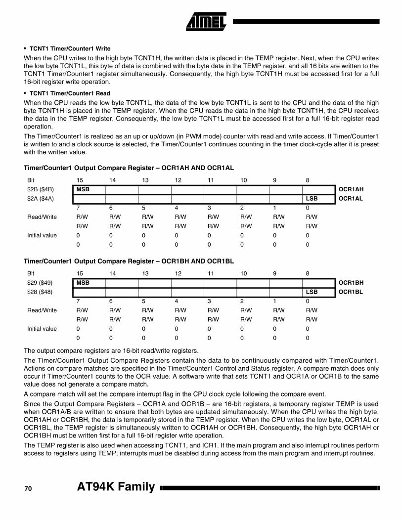
• TCNT1 Timer/Counter1 Write
When the CPU writes to the high byte TCNT1H, the written data is placed in the TEMP register. Next, when the CPU writesthe low byte TCNT1L, this byte of data is combined with the byte data in the TEMP register, and all 16 bits are written to theTCNT1 Timer/Counter1 register simultaneously. Consequently, the high byte TCNT1H must be accessed first for a full16-bit register write operation.
• TCNT1 Timer/Counter1 Read
When the CPU reads the low byte TCNT1L, the data of the low byte TCNT1L is sent to the CPU and the data of the highbyte TCNT1H is placed in the TEMP register. When the CPU reads the data in the high byte TCNT1H, the CPU receivesthe data in the TEMP register. Consequently, the low byte TCNT1L must be accessed first for a full 16-bit register readoperation.
The Timer/Counter1 is realized as an up or up/down (in PWM mode) counter with read and write access. If Timer/Counter1is written to and a clock source is selected, the Timer/Counter1 continues counting in the timer clock-cycle after it is presetwith the written value.
Timer/Counter1 Output Compare Register – OCR1AH AND OCR1AL
Timer/Counter1 Output Compare Register – OCR1BH AND OCR1BL
The output compare registers are 16-bit read/write registers.
The Timer/Counter1 Output Compare Registers contain the data to be continuously compared with Timer/Counter1.Actions on compare matches are specified in the Timer/Counter1 Control and Status register. A compare match does onlyoccur if Timer/Counter1 counts to the OCR value. A software write that sets TCNT1 and OCR1A or OCR1B to the samevalue does not generate a compare match.
A compare match will set the compare interrupt flag in the CPU clock cycle following the compare event.
Since the Output Compare Registers – OCR1A and OCR1B – are 16-bit registers, a temporary register TEMP is usedwhen OCR1A/B are written to ensure that both bytes are updated simultaneously. When the CPU writes the high byte,OCR1AH or OCR1BH, the data is temporarily stored in the TEMP register. When the CPU writes the low byte, OCR1AL orOCR1BL, the TEMP register is simultaneously written to OCR1AH or OCR1BH. Consequently, the high byte OCR1AH orOCR1BH must be written first for a full 16-bit register write operation.
The TEMP register is also used when accessing TCNT1, and ICR1. If the main program and also interrupt routines performaccess to registers using TEMP, interrupts must be disabled during access from the main program and interrupt routines.
Bit 15 14 13 12 11 10 9 8
$2B ($4B) MSB OCR1AH
$2A ($4A) LSB OCR1AL
7 6 5 4 3 2 1 0
Read/Write R/W R/W R/W R/W R/W R/W R/W R/W
R/W R/W R/W R/W R/W R/W R/W R/W
Initial value 0 0 0 0 0 0 0 0
0 0 0 0 0 0 0 0
Bit 15 14 13 12 11 10 9 8
$29 ($49) MSB OCR1BH
$28 ($48) LSB OCR1BL
7 6 5 4 3 2 1 0
Read/Write R/W R/W R/W R/W R/W R/W R/W R/W
R/W R/W R/W R/W R/W R/W R/W R/W
Initial value 0 0 0 0 0 0 0 0
0 0 0 0 0 0 0 0
AT94K Family70
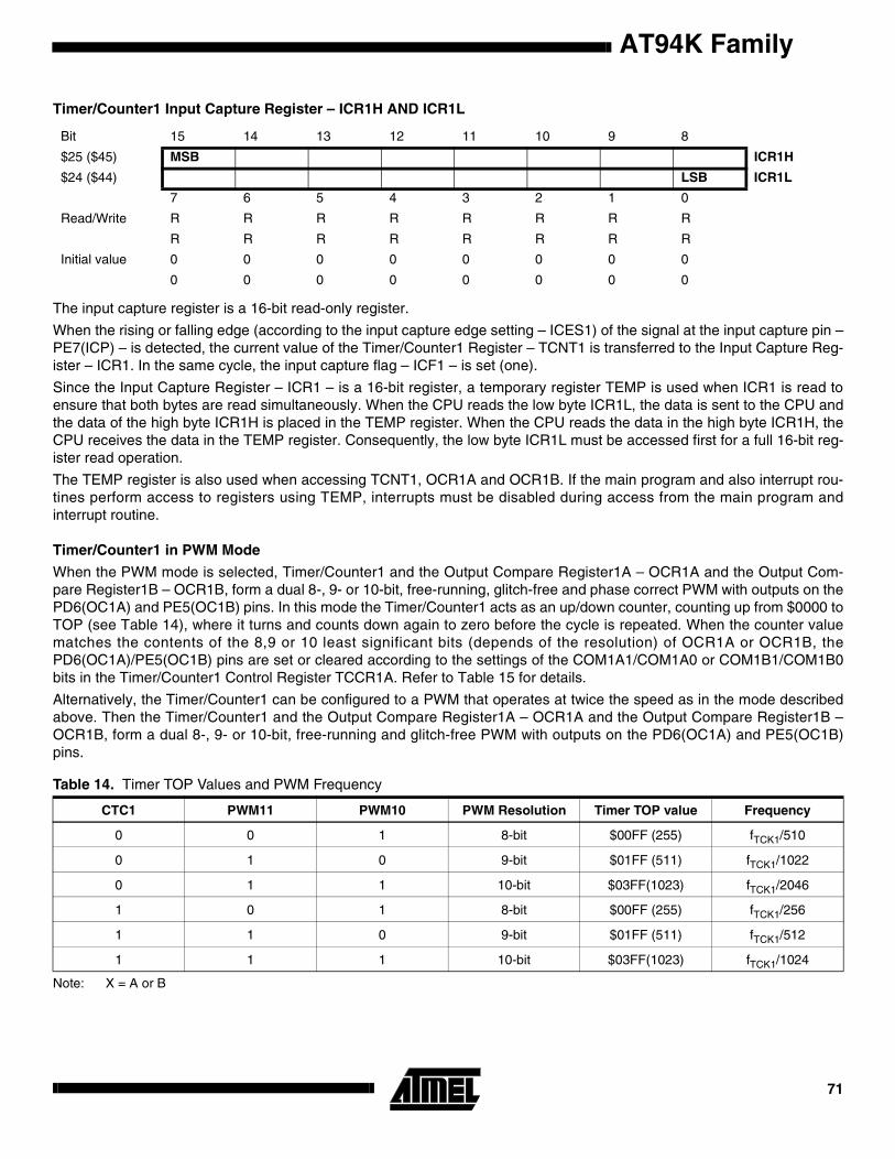
AT94K Family
Timer/Counter1 Input Capture Register – ICR1H AND ICR1L
The input capture register is a 16-bit read-only register.
When the rising or falling edge (according to the input capture edge setting – ICES1) of the signal at the input capture pin –PE7(ICP) – is detected, the current value of the Timer/Counter1 Register – TCNT1 is transferred to the Input Capture Reg-ister – ICR1. In the same cycle, the input capture flag – ICF1 – is set (one).
Since the Input Capture Register – ICR1 – is a 16-bit register, a temporary register TEMP is used when ICR1 is read toensure that both bytes are read simultaneously. When the CPU reads the low byte ICR1L, the data is sent to the CPU andthe data of the high byte ICR1H is placed in the TEMP register. When the CPU reads the data in the high byte ICR1H, theCPU receives the data in the TEMP register. Consequently, the low byte ICR1L must be accessed first for a full 16-bit reg-ister read operation.
The TEMP register is also used when accessing TCNT1, OCR1A and OCR1B. If the main program and also interrupt rou-tines perform access to registers using TEMP, interrupts must be disabled during access from the main program andinterrupt routine.
Timer/Counter1 in PWM Mode
When the PWM mode is selected, Timer/Counter1 and the Output Compare Register1A – OCR1A and the Output Com-pare Register1B – OCR1B, form a dual 8-, 9- or 10-bit, free-running, glitch-free and phase correct PWM with outputs on thePD6(OC1A) and PE5(OC1B) pins. In this mode the Timer/Counter1 acts as an up/down counter, counting up from $0000 toTOP (see Table 14), where it turns and counts down again to zero before the cycle is repeated. When the counter valuematches the contents of the 8,9 or 10 least significant bits (depends of the resolution) of OCR1A or OCR1B, thePD6(OC1A)/PE5(OC1B) pins are set or cleared according to the settings of the COM1A1/COM1A0 or COM1B1/COM1B0bits in the Timer/Counter1 Control Register TCCR1A. Refer to Table 15 for details.
Alternatively, the Timer/Counter1 can be configured to a PWM that operates at twice the speed as in the mode describedabove. Then the Timer/Counter1 and the Output Compare Register1A – OCR1A and the Output Compare Register1B –OCR1B, form a dual 8-, 9- or 10-bit, free-running and glitch-free PWM with outputs on the PD6(OC1A) and PE5(OC1B)pins.
Note: X = A or B
Bit 15 14 13 12 11 10 9 8
$25 ($45) MSB ICR1H
$24 ($44) LSB ICR1L
7 6 5 4 3 2 1 0
Read/Write R R R R R R R R
R R R R R R R R
Initial value 0 0 0 0 0 0 0 0
0 0 0 0 0 0 0 0
Table 14. Timer TOP Values and PWM Frequency
CTC1 PWM11 PWM10 PWM Resolution Timer TOP value Frequency
0 0 1 8-bit $00FF (255) fTCK1/510
0 1 0 9-bit $01FF (511) fTCK1/1022
0 1 1 10-bit $03FF(1023) fTCK1/2046
1 0 1 8-bit $00FF (255) fTCK1/256
1 1 0 9-bit $01FF (511) fTCK1/512
1 1 1 10-bit $03FF(1023) fTCK1/1024
71
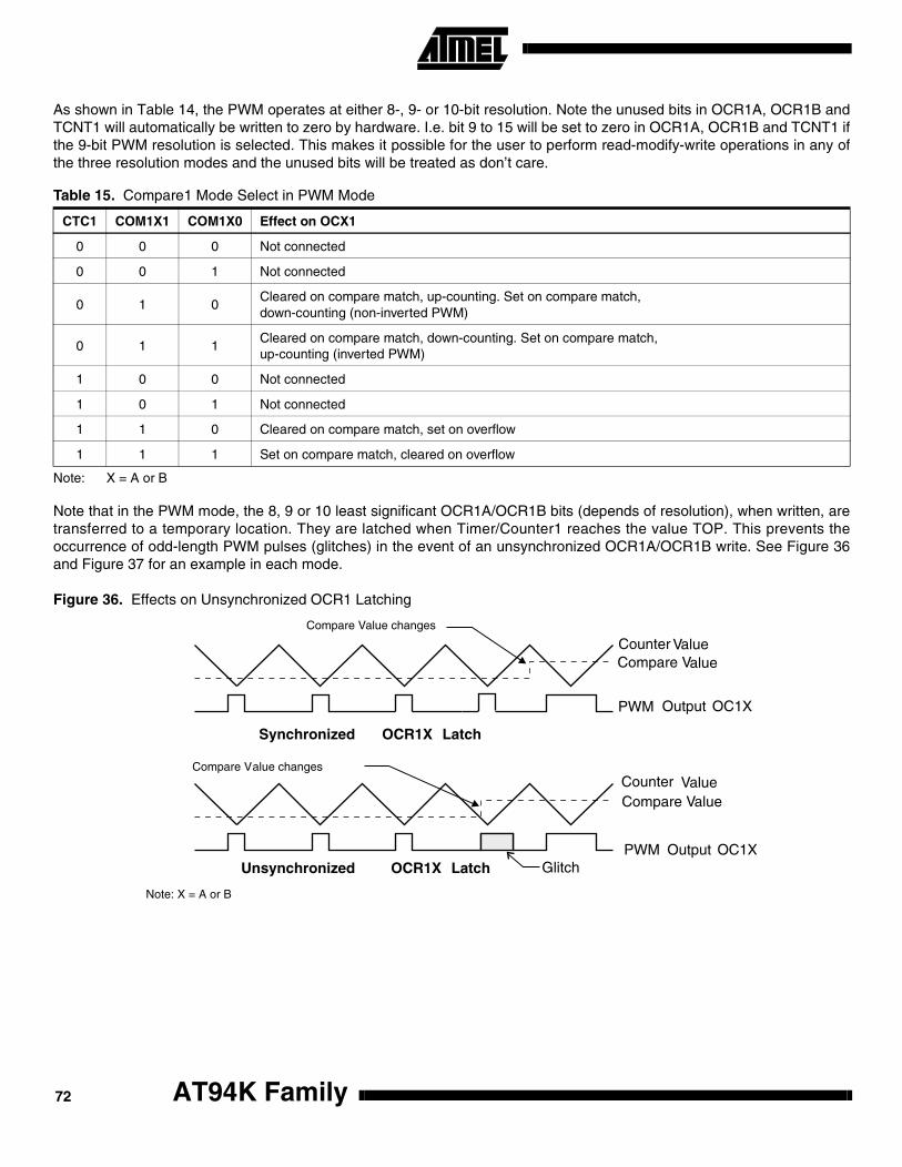
As shown in Table 14, the PWM operates at either 8-, 9- or 10-bit resolution. Note the unused bits in OCR1A, OCR1B andTCNT1 will automatically be written to zero by hardware. I.e. bit 9 to 15 will be set to zero in OCR1A, OCR1B and TCNT1 ifthe 9-bit PWM resolution is selected. This makes it possible for the user to perform read-modify-write operations in any ofthe three resolution modes and the unused bits will be treated as don’t care.
Note: X = A or B
Note that in the PWM mode, the 8, 9 or 10 least significant OCR1A/OCR1B bits (depends of resolution), when written, aretransferred to a temporary location. They are latched when Timer/Counter1 reaches the value TOP. This prevents theoccurrence of odd-length PWM pulses (glitches) in the event of an unsynchronized OCR1A/OCR1B write. See Figure 36and Figure 37 for an example in each mode.
Figure 36. Effects on Unsynchronized OCR1 Latching
Table 15. Compare1 Mode Select in PWM Mode
CTC1 COM1X1 COM1X0 Effect on OCX1
0 0 0 Not connected
0 0 1 Not connected
0 1 0Cleared on compare match, up-counting. Set on compare match, down-counting (non-inverted PWM)
0 1 1Cleared on compare match, down-counting. Set on compare match, up-counting (inverted PWM)
1 0 0 Not connected
1 0 1 Not connected
1 1 0 Cleared on compare match, set on overflow
1 1 1 Set on compare match, cleared on overflow
Counter ValueCompare Value
PWM Output OC1X
Synchronized OCR1X Latch
Counter ValueCompare Value
PWM Output OC1XUnsynchronized OCR1X Latch Glitch
Compare Value changes
Note: X = A or B
Compare Value changes
AT94K Family72
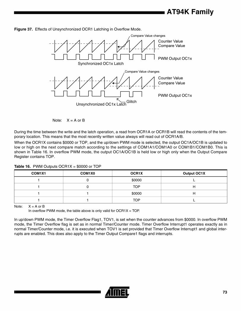
AT94K Family
Figure 37. Effects of Unsynchronized OCR1 Latching in Overflow Mode.
During the time between the write and the latch operation, a read from OCR1A or OCR1B will read the contents of the tem-porary location. This means that the most recently written value always will read out of OCR1A/B.
When the OCR1X contains $0000 or TOP, and the up/down PWM mode is selected, the output OC1A/OC1B is updated tolow or high on the next compare match according to the settings of COM1A1/COM1A0 or COM1B1/COM1B0. This isshown in Table 16. In overflow PWM mode, the output OC1A/OC1B is held low or high only when the Output CompareRegister contains TOP.
Note: X = A or BIn overflow PWM mode, the table above is only valid for OCR1X = TOP.
In up/down PWM mode, the Timer Overflow Flag1, TOV1, is set when the counter advances from $0000. In overflow PWMmode, the Timer Overflow flag is set as in normal Timer/Counter mode. Timer Overflow Interrupt1 operates exactly as innormal Timer/Counter mode, i.e. it is executed when TOV1 is set provided that Timer Overflow Interrupt1 and global inter-rupts are enabled. This does also apply to the Timer Output Compare1 flags and interrupts.
Table 16. PWM Outputs OCR1X = $0000 or TOP
COM1X1 COM1X0 OCR1X Output OC1X
1 0 $0000 L
1 0 TOP H
1 1 $0000 H
1 1 TOP L
PWM Output OC1x
PWM Output OC1x
Unsynchronized OC1x Latch
Synchronized OC1x Latch
Note: X = A or B
73
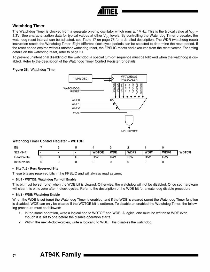
Watchdog TimerThe Watchdog Timer is clocked from a separate on-chip oscillator which runs at 1MHz. This is the typical value at VCC =3.3V. See characterization data for typical values at other VCC levels. By controlling the Watchdog Timer prescaler, thewatchdog reset interval can be adjusted, see Table 17 on page 75 for a detailed description. The WDR (watchdog reset)instruction resets the Watchdog Timer. Eight different clock cycle periods can be selected to determine the reset period. Ifthe reset period expires without another watchdog reset, the FPSLIC resets and executes from the reset vector. For timingdetails on the watchdog reset, refer to page 51.
To prevent unintentional disabling of the watchdog, a special turn-off sequence must be followed when the watchdog is dis-abled. Refer to the description of the Watchdog Timer Control Register for details.
Figure 38. Watchdog Timer
Watchdog Timer Control Register – WDTCR
• Bits 7..5 - Res: Reserved Bits
These bits are reserved bits in the FPSLIC and will always read as zero.
• Bit 4 - WDTOE: Watchdog Turn-off Enable
This bit must be set (one) when the WDE bit is cleared. Otherwise, the watchdog will not be disabled. Once set, hardwarewill clear this bit to zero after 4-clock-cycles. Refer to the description of the WDE bit for a watchdog disable procedure.
• Bit 3 - WDE: Watchdog Enable
When the WDE is set (one) the Watchdog Timer is enabled, and if the WDE is cleared (zero) the Watchdog Timer functionis disabled. WDE can only be cleared if the WDTOE bit is set(one). To disable an enabled the Watchdog Timer, the follow-ing procedure must be followed:
1. In the same operation, write a logical one to WDTOE and WDE. A logical one must be written to WDE even though it is set to one before the disable operation starts.
2. Within the next 4-clock-cycles, write a logical 0 to WDE. This disables the watchdog.
Bit 7 6 5 4 3 2 1 0
$21 ($41) - - - WDTOE WDE WDP2 WDP1 WDP0 WDTCR
Read/Write R R R R/W R/W R/W R/W R/W
Initial value 0 0 0 0 0 0 0 0
AT94K Family74

AT94K Family
• Bits 2..0 - WDP2, WDP1, WDP0: Watchdog Timer Prescaler 2, 1 and 0
The WDP2, WDP1 and WDP0 bits determine the Watchdog Timer prescaling when the Watchdog Timer is enabled. Thedifferent prescaling values and their corresponding Time-out periods are shown in Table 17.
Note: The frequency of the watchdog oscillator is voltage dependent as shown in the Electrical Characteristics section.The WDR (watchdog reset) instruction should always be executed before the Watchdog Timer is enabled. This ensures that the reset period will be in accordance with the Watchdog Timer prescale settings. If the Watchdog Timer is enabled without reset, the Watchdog Timer may not start counting from zero.
UARTsThe FPSLIC features two full duplex (separate receive and transmit registers) Universal Asynchronous Receiver andTransmitter (UART). The main features are:• Baud-rate Generator Generates any Baud-rate
• High Baud-rates at Low XTAL Frequencies
• 8 or 9 Bits Data
• Noise Filtering
• Overrun Detection
• Framing Error Detection
• False Start Bit Detection
• Three Separate Interrupts on TX Complete, TX Data Register Empty and RX Complete
• Multi-processor Communication Mode
• Double Speed UART Mode
Table 17. Watchdog Timer Prescale Select
WDP2 WDP1 WDP0Number of WDTOscillator cycles
Typical Time-out at VCC = 3.0V
0 0 0 16K cycles 47 ms
0 0 1 32K cycles 94 ms
0 1 0 64K cycles 0.19 s
0 1 1 128K cycles 0.38 s
1 0 0 256K cycles 0.75 s
1 0 1 512K cycles 1.5 s
1 1 0 1,024K cycles 3.0 s
1 1 1 2,048K cycles 6.0 s
75

Data TransmissionA block schematic of the UART transmitter is shown in Figure 39. The two UARTs are identical and the functionality isdescribed in general for the two UARTs.
Figure 39. UART Transmitter
Data transmission is initiated by writing the data to be transmitted to the UART I/O Data Register, UDRn. Data is trans-ferred from UDRn to the Transmit shift register when:• A new character has been written to UDRn after the stop bit from the previous character has been shifted out. The shift
register is loaded immediately.
• A new character has been written to UDRn before the stop bit from the previous character has been shifted out. The shift register is loaded when the stop bit of the character currently being transmitted has been shifted out.
If the 10(11)-bit Transmitter shift register is empty, data is transferred from UDRn to the shift register. At this time theUDREn (UART Data Register Empty) bit in the UART Control and Status Register, UCSRnA, is set. When this bit is set(one), the UART is ready to receive the next character. At the same time as the data is transferred from UDRn to the10(11)-bit shift register, bit 0 of the shift register is cleared (start bit) and bit 9 or 10 is set (stop bit). If 9 bit data word isselected (the CHR9n bit in the UART Control and Status Register, UCSRnB is set), the TXB8 bit in UCSRnB is transferredto bit 9 in the Transmit shift register.
On the Baud-rate clock following the transfer operation to the shift register, the start bit is shifted out on the TXDn pin. Thenfollows the data, LSB first. When the stop bit has been shifted out, the shift register is loaded if any new data has been writ-ten to the UDRn during the transmission. During loading, UDREn is set. If there is no new data in the UDRn register to send
PE0/PE2
U2X
n
10(11)-BIT TXSHIFT REGISTER
PIN CONTROLLOGIC
UART CONTROL ANDSTATUS REGISTER
(UCSRnA)
UART CONTROL ANDSTATUS REGISTER
(UCSRnB)
CONTROL LOGIC
BAUD RATEGENERATOR
TXCnIRQ
UDREnIRQ
DATA BUSRX
CIE
n
TX
CIE
n
UD
RIE
n
TX
Cn
UD
RE
n
RX
EN
nT
XE
Nn
CH
R9n
RX
B8n
TX
B8n
RX
Cn
TX
Cn
UD
RE
nF
En
MP
CM
Pn
OR
n
IDLE
BAUD
STORE UDRnSHIFT ENABLE
DATA BUS
BAUD x 16/16 UART I/O DATA
REGISTER (UDRn)XTAL
TXDn
n = 0,1
AT94K Family76
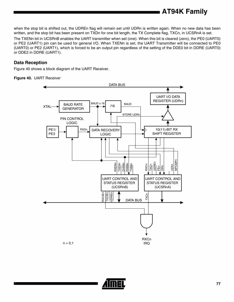
AT94K Family
when the stop bit is shifted out, the UDREn flag will remain set until UDRn is written again. When no new data has beenwritten, and the stop bit has been present on TXDn for one bit length, the TX Complete flag, TXCn, in UCSRnA is set.
The TXENn bit in UCSRnB enables the UART transmitter when set (one). When this bit is cleared (zero), the PE0 (UART0)or PE2 (UART1) pin can be used for general I/O. When TXENn is set, the UART Transmitter will be connected to PE0(UART0) or PE2 (UART1), which is forced to be an output pin regardless of the setting of the DDE0 bit in DDRE (UART0)or DDE2 in DDRE (UART1).
Data ReceptionFigure 40 shows a block diagram of the UART Receiver.
Figure 40. UART Receiver
PE1/PE3
DATA BUS
BAUD
UART I/O DATAREGISTER (UDRn)
10(11)-BIT RXSHIFT REGISTER
STORE UDRn
/16BAUD x 16
RX
EN
nT
XE
Nn
CH
R9n
RX
B8n
TX
B8n
U2X
n
RX
Cn
TX
Cn
UD
RE
nF
En
MP
CM
Pn
OR
n
UART CONTROL ANDSTATUS REGISTER
(UCSRnB)
UART CONTROL ANDSTATUS REGISTER
(UCSRnA)
RX
CIE
n
TX
CIE
n
UD
RIE
n
TX
Cn
DATA BUS
PIN CONTROLLOGIC
BAUD RATEGENERATOR
XTAL
n = 0,1RXCnIRQ
DATA RECOVERYLOGIC
RXDn
77
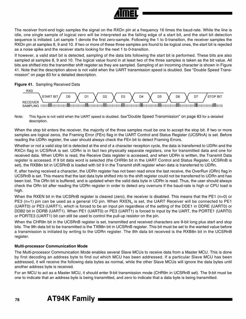
The receiver front-end logic samples the signal on the RXDn pin at a frequency 16 times the baud-rate. While the line isidle, one single sample of logical zero will be interpreted as the falling edge of a start bit, and the start bit detectionsequence is initiated. Let sample 1 denote the first zero-sample. Following the 1 to 0-transition, the receiver samples theRXDn pin at samples 8, 9 and 10. If two or more of these three samples are found to be logical ones, the start bit is rejectedas a noise spike and the receiver starts looking for the next 1 to 0-transition.
If however, a valid start bit is detected, sampling of the data bits following the start bit is performed. These bits are alsosampled at samples 8, 9 and 10. The logical value found in at least two of the three samples is taken as the bit value. Allbits are shifted into the transmitter shift register as they are sampled. Sampling of an incoming character is shown in Figure41. Note that the description above is not valid when the UART transmission speed is doubled. See “Double Speed Trans-mission” on page 83 for a detailed description.
Figure 41. Sampling Received Data
Note: This figure is not valid when the UART speed is doubled. See“Double Speed Transmission” on page 83 for a detailed description.
When the stop bit enters the receiver, the majority of the three samples must be one to accept the stop bit. If two or moresamples are logical zeros, the Framing Error (FEn) flag in the UART Control and Status Register (UCSRnA) is set. Beforereading the UDRn register, the user should always check the FEn bit to detect Framing Errors.
Whether or not a valid stop bit is detected at the end of a character reception cycle, the data is transferred to UDRn and theRXCn flag in UCSRnA is set. UDRn is in fact two physically separate registers, one for transmitted data and one forreceived data. When UDRn is read, the Receive Data register is accessed, and when UDRn is written, the Transmit Dataregister is accessed. If 9 bit data word is selected (the CHR9n bit in the UART Control and Status Register, UCSRnB isset), the RXB8n bit in UCSRnB is loaded with bit 9 in the Transmit shift register when data is transferred to UDRn.
If, after having received a character, the UDRn register has not been read since the last receive, the OverRun (ORn) flag inUCSRnB is set. This means that the last data byte shifted into to the shift register could not be transferred to UDRn and hasbeen lost. The ORn bit is buffered, and is updated when the valid data byte in UDRn is read. Thus, the user should alwayscheck the ORn bit after reading the UDRn register in order to detect any overruns if the baud-rate is high or CPU load ishigh.
When the RXEN bit in the UCSRnB register is cleared (zero), the receiver is disabled. This means that the PE1 (n=0) orPE3 (n=1) pin can be used as a general I/O pin. When RXENn is set, the UART Receiver will be connected to PE1(UART0) or PE3 (UART1), which is forced to be an input pin regardless of the setting of the DDE1 in DDRE (UART0) orDDB2 bit in DDRB (UART1). When PE1 (UART0) or PE3 (UART1) is forced to input by the UART, the PORTE1 (UART0)or PORTE3 (UART1) bit can still be used to control the pull-up resistor on the pin.
When the CHR9n bit in the UCSRnB register is set, transmitted and received characters are 9-bit long plus start and stopbits. The 9th data bit to be transmitted is the TXB8n bit in UCSRnB register. This bit must be set to the wanted value beforea transmission is initiated by writing to the UDRn register. The 9th data bit received is the RXB8n bit in the UCSRnBregister.
Multi-processor Communication Mode
The Multi-processor Communication Mode enables several Slave MCUs to receive data from a Master MCU. This is doneby first decoding an address byte to find out which MCU has been addressed. If a particular Slave MCU has beenaddressed, it will receive the following data bytes as normal, while the other Slave MCUs will ignore the data bytes untilanother address byte is received.
For an MCU to act as a Master MCU, it should enter 9-bit transmission mode (CHR9n in UCSRnB set). The 9-bit must beone to indicate that an address byte is being transmitted, and zero to indicate that a data byte is being transmitted.
AT94K Family78

AT94K Family
For the Slave MCUs, the mechanism appears slightly differently for 8-bit and 9-bit reception mode. In 8-bit reception mode(CHR9n in UCSRnB cleared), the stop bit is one for an address byte and zero for a data byte. In 9-bit reception mode(CHR9n in UCSRnB set), the 9-bit is one for an address byte and zero for a data byte, whereas the stop bit is always high.
The following procedure should be used to exchange data in Multi-processor Communication Mode:
1. All Slave MCUs are in Multi-processor Communication Mode (MPCMn in UCSRnA is set).
2. The Master MCU sends an address byte, and all Slaves receive and read this byte. In the Slave MCUs, the RXCn flag in UCSRnA will be set as normal.
3. Each Slave MCU reads the UDRn register and determines if it has been selected. If so, it clears the MPCMn bit in UCSRnA, otherwise it waits for the next address byte.
4. For each received data byte, the receiving MCU will set the receive complete flag (RXCn in UCSRnA. In 8-bit mode, the receiving MCU will also generate a framing error (FEn in UCSRnA set), since the stop bit is zero. The other Slave MCUs, which still have the MPCMn bit set, will ignore the data byte. In this case, the UDRn register and the RXCn, FEn, or flags will not be affected.
5. After the last byte has been transferred, the process repeats from step 2.
UART Control
UART0 I/O Data Register – UDR0
UART1 I/O Data Register – UDR1
The UDRn register is actually two physically separate registers sharing the same I/O address. When writing to the register,the UART Transmit Data register is written. When reading from UDRn, the UART Receive Data register is read.
UART0 Control and Status Registers – UCSR0A
UART1 Control and Status Registers – UCSR1A
Bit 7 6 5 4 3 2 1 0
$0C ($2C) MSB LSB UDR0
Read/Write R/W R/W R/W R/W R/W R/W R/W R/W
Initial value 0 0 0 0 0 0 0 0
Bit 7 6 5 4 3 2 1 0
$03 ($23) MSB LSB UDR1
Read/Write R/W R/W R/W R/W R/W R/W R/W R/W
Initial value 0 0 0 0 0 0 0 0
Bit 7 6 5 4 3 2 1 0
$0B ($2B) RXC0 TXC0 UDRE0 FE0 OR0 - U2X0 MPCM0 UCSR0A
Read/Write R R/W R R R R R/W R/W
Initial value 0 0 1 0 0 0 0 0
Bit 7 6 5 4 3 2 1 0
$02 ($22) RXC1 TXC1 UDRE1 FE1 OR1 - U2X1 MPCM1 UCSR1A
Read/Write R R/W R R R R R/W R/W
Initial value 0 0 1 0 0 0 0 0
79

• Bit 7 - RXC0/RXC1: UART Receive Complete
This bit is set (one) when a received character is transferred from the Receiver Shift register to UDRn. The bit is set regard-less of any detected framing errors. When the RXCIEn bit in UCSRnB is set, the UART Receive Complete interrupt will beexecuted when RXCn is set(one). RXCn is cleared by reading UDRn. When interrupt-driven data reception is used, theUART Receive Complete Interrupt routine must read UDRn in order to clear RXCn, otherwise a new interrupt will occuronce the interrupt routine terminates.
• Bit 6 - TXC0/TXC1: UART Transmit Complete
This bit is set (one) when the entire character (including the stop bit) in the Transmit Shift register has been shifted out andno new data has been written to UDRn. This flag is especially useful in half-duplex communications interfaces, where atransmitting application must enter receive mode and free the communications bus immediately after completing thetransmission.
When the TXCIEn bit in UCSRnB is set, setting of TXCn causes the UART Transmit Complete interrupt to be executed.TXCn is cleared by hardware when executing the corresponding interrupt handling vector. Alternatively, the TXCn bit iscleared (zero) by writing a logical one to the bit.
• Bit 5 - UDRE0/UDRE1: UART Data Register Empty
This bit is set (one) when a character written to UDRn is transferred to the Transmit shift register. Setting of this bit indi-cates that the transmitter is ready to receive a new character for transmission.
When the UDRIEn bit in UCSRnB is set, the UART Transmit Complete interrupt will be executed as long as UDREn is setand the global interrupt enable bit in SREG is set. UDREn is cleared by writing UDRn. When interrupt-driven data transmit-tal is used, the UART Data Register Empty Interrupt routine must write UDRn in order to clear UDREn, otherwise a newinterrupt will occur once the interrupt routine terminates.
UDREn is set (one) during reset to indicate that the transmitter is ready.
• Bit 4 - FE0/FE1: Framing Error
This bit is set if a Framing Error condition is detected, i.e. when the stop bit of an incoming character is zero.
The FEn bit is cleared when the stop bit of received data is one.
• Bit 3 - OR0/OR1: OverRun
This bit is set if an Overrun condition is detected, i.e. when a character already present in the UDRn register is not readbefore the next character has been shifted into the Receiver Shift register. The ORn bit is buffered, which means that it willbe set once the valid data still in UDRn is read.
The ORn bit is cleared (zero) when data is received and transferred to UDRn.
• Bit 2 - Res: Reserved Bit
This bit is reserved bit in the FPSLIC and will always read as zero.
• Bits 1 - U2X0/U2X1: Double the UART Transmission Speed
When this bit is set (one) the UART speed will be doubled. This means that a bit will be transmitted/received in 8 CPU clockperiods instead of 16 CPU clock periods. For a detailed description, see “Double Speed Transmission” on page 83”.
• Bit 0 - MPCM0/MPCM1: Multi-processor Communication Mode
This bit is used to enter Multi-processor Communication Mode. The bit is set when the Slave MCU waits for an addressbyte to be received. When the MCU has been addressed, the MCU switches off the MPCMn bit, and starts data reception.
For a detailed description, see “Multi-processor Communication Mode”.
AT94K Family80
AT94K Family
UART0 Control and Status Registers – UCSR0B
UART1 Control and Status Registers – UCSR1B
• Bit 7 - RXCIE0/RXCIE1: RX Complete Interrupt Enable
When this bit is set (one), a setting of the RXCn bit in UCSRnA will cause the Receive Complete interrupt routine to beexecuted provided that global interrupts are enabled.
• Bit 6 - TXCIE0/TXCIE1: TX Complete Interrupt Enable
When this bit is set (one), a setting of the TXCn bit in UCSRnA will cause the Transmit Complete interrupt routine to beexecuted provided that global interrupts are enabled.
• Bit 5 - UDRIE0/UDREI1: UART Data Register Empty Interrupt Enable
When this bit is set (one), a setting of the UDREn bit in UCSRnA will cause the UART Data Register Empty interrupt routineto be executed provided that global interrupts are enabled.
• Bit 4 - RXEN0/RXEN1: Receiver Enable
This bit enables the UART receiver when set (one). When the receiver is disabled, the TXCn, ORn and FEn status flagscannot become set. If these flags are set, turning off RXENn does not cause them to be cleared.
• Bit 3 - TXEN0/TXEN1: Transmitter Enable
This bit enables the UART transmitter when set (one). When disabling the transmitter while transmitting a character, thetransmitter is not disabled before the character in the shift register plus any following character in UDRn has been com-pletely transmitted.
• Bit 2 - CHR90/CHR91: 9-bit Characters
When this bit is set (one) transmitted and received characters are 9-bit long plus start and stop bits. The 9-bit is read andwritten by using the RXB8n and TXB8 bits in UCSRnB, respectively. The 9th data bit can be used as an extra stop bit or aparity bit.
• Bit 1 - RXB80/RXB81: Receive Data Bit 8
When CHR9n is set (one), RXB8n is the 9th data bit of the received character.
• Bit 0 - TXB80/TXB81: Transmit Data Bit 8
When CHR9n is set (one), TXB8n is the 9th data bit in the character to be transmitted.
Baud-rate Generator
The baud-rate generator is a frequency divider which generates baud-rates according to the following equation:
• BAUD = Baud-rate
• fCK= Crystal Clock frequency
• UBR = Contents of the UBRRHI and UBRRn registers, (0-4095)
Bit 7 6 5 4 3 2 1 0
$0A ($2A) RXCIE0 TXCIE0 UDRIE0 RXEN0 TXEN0 CHR90 RXB80 TXB80 UCSR0B
Read/Write R/W R/W R/W R/W R/W R/W R R/W
Initial value 0 0 0 0 0 0 1 0
Bit 7 6 5 4 3 2 1 0
$01 ($21) RXCIE1 TXCIE1 UDRIE1 RXEN1 TXEN1 CHR91 RXB81 TXB81 UCSR1B
Read/Write R/W R/W R/W R/W R/W R/W R R/W
Initial value 0 0 0 0 0 0 1 0
BAUDfCK
16(UBR 1 )+---------------------------------=
81
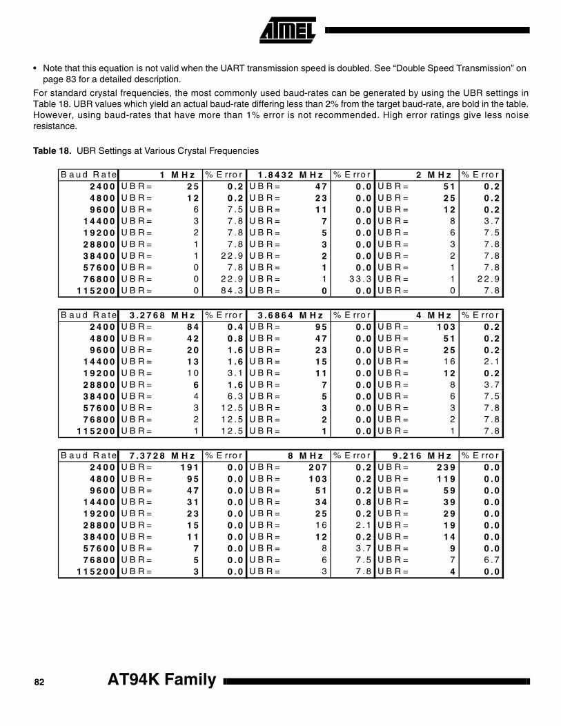
• Note that this equation is not valid when the UART transmission speed is doubled. See “Double Speed Transmission” on page 83 for a detailed description.
For standard crystal frequencies, the most commonly used baud-rates can be generated by using the UBR settings inTable 18. UBR values which yield an actual baud-rate differing less than 2% from the target baud-rate, are bold in the table.However, using baud-rates that have more than 1% error is not recommended. High error ratings give less noiseresistance.
Table 18. UBR Settings at Various Crystal Frequencies
B a u d R a t e 1 M H z % E rro r 1 . 8 4 3 2 M H z % E rro r 2 M H z % E rro r2 4 0 0 U B R = 2 5 0 . 2 U B R = 4 7 0 . 0 U B R = 5 1 0 . 24 8 0 0 U B R = 1 2 0 . 2 U B R = 2 3 0 . 0 U B R = 2 5 0 . 29 6 0 0 U B R = 6 7 . 5 U B R = 1 1 0 . 0 U B R = 1 2 0 . 2
1 4 4 0 0 U B R = 3 7 . 8 U B R = 7 0 . 0 U B R = 8 3 . 71 9 2 0 0 U B R = 2 7 . 8 U B R = 5 0 . 0 U B R = 6 7 . 52 8 8 0 0 U B R = 1 7 . 8 U B R = 3 0 . 0 U B R = 3 7 . 83 8 4 0 0 U B R = 1 2 2 . 9 U B R = 2 0 . 0 U B R = 2 7 . 85 7 6 0 0 U B R = 0 7 . 8 U B R = 1 0 . 0 U B R = 1 7 . 87 6 8 0 0 U B R = 0 2 2 . 9 U B R = 1 3 3 . 3 U B R = 1 2 2 . 9
1 1 5 2 0 0 U B R = 0 8 4 . 3 U B R = 0 0 . 0 U B R = 0 7 . 8
B a u d R a t e 3 . 2 7 6 8 M H z % E rro r 3 . 6 8 6 4 M H z % E rro r 4 M H z % E rro r2 4 0 0 U B R = 8 4 0 . 4 U B R = 9 5 0 . 0 U B R = 1 0 3 0 . 24 8 0 0 U B R = 4 2 0 . 8 U B R = 4 7 0 . 0 U B R = 5 1 0 . 29 6 0 0 U B R = 2 0 1 . 6 U B R = 2 3 0 . 0 U B R = 2 5 0 . 2
1 4 4 0 0 U B R = 1 3 1 . 6 U B R = 1 5 0 . 0 U B R = 1 6 2 . 11 9 2 0 0 U B R = 1 0 3 . 1 U B R = 1 1 0 . 0 U B R = 1 2 0 . 22 8 8 0 0 U B R = 6 1 . 6 U B R = 7 0 . 0 U B R = 8 3 . 73 8 4 0 0 U B R = 4 6 . 3 U B R = 5 0 . 0 U B R = 6 7 . 55 7 6 0 0 U B R = 3 1 2 . 5 U B R = 3 0 . 0 U B R = 3 7 . 87 6 8 0 0 U B R = 2 1 2 . 5 U B R = 2 0 . 0 U B R = 2 7 . 8
1 1 5 2 0 0 U B R = 1 1 2 . 5 U B R = 1 0 . 0 U B R = 1 7 . 8
B a u d R a t e 7 . 3 7 2 8 M H z % E rro r 8 M H z % E rro r 9 . 2 1 6 M H z % E rro r2 4 0 0 U B R = 1 9 1 0 . 0 U B R = 2 0 7 0 . 2 U B R = 2 3 9 0 . 04 8 0 0 U B R = 9 5 0 . 0 U B R = 1 0 3 0 . 2 U B R = 1 1 9 0 . 09 6 0 0 U B R = 4 7 0 . 0 U B R = 5 1 0 . 2 U B R = 5 9 0 . 0
1 4 4 0 0 U B R = 3 1 0 . 0 U B R = 3 4 0 . 8 U B R = 3 9 0 . 01 9 2 0 0 U B R = 2 3 0 . 0 U B R = 2 5 0 . 2 U B R = 2 9 0 . 02 8 8 0 0 U B R = 1 5 0 . 0 U B R = 1 6 2 . 1 U B R = 1 9 0 . 03 8 4 0 0 U B R = 1 1 0 . 0 U B R = 1 2 0 . 2 U B R = 1 4 0 . 05 7 6 0 0 U B R = 7 0 . 0 U B R = 8 3 . 7 U B R = 9 0 . 07 6 8 0 0 U B R = 5 0 . 0 U B R = 6 7 . 5 U B R = 7 6 . 7
1 1 5 2 0 0 U B R = 3 0 . 0 U B R = 3 7 . 8 U B R = 4 0 . 0
AT94K Family82

AT94K Family
UART0 and UART1 High byte Baud-rate Register UBRRHI
The UART baud register is a 12-bit register. The 4 most significant bits are located in a separate register, UBRRHI. Notethat both UART0 and UART1 share this register. Bit 7 to bit 4 of UBRRHI contain the 4 most significant bits of the UART1baud register. Bit3 to Bit0 contain the 4 most significant bits of the UART0 baud register.
UART0 Baud-rate Register Low Byte – UBRR0
UART1 Baud-rate Register Low Byte – UBRR1
UBRRn stores the 8 least significant bits of the UART baud-rate register.
Double Speed TransmissionThe FPSLIC provides a separate UART mode that allows the user to double the communication speed. By setting the U2Xbit in UART Control and Status Register UCSRnA, the UART speed will be doubled. The data reception will differ slightlyfrom normal mode. Since the speed is doubled, the receiver front-end logic samples the signals on RXDn pin at a fre-quency 8 times the baud-rate. While the line is idle, one single sample of logical zero will be interpreted as the falling edgeof a start bit, and the start bit detection sequence is initiated. Let sample 1 denote the first zero-sample. Following the 1 to0-transition, the receiver samples the RXDn pin at samples 4, 5 and 6. If two or more of these three samples are found tobe logical ones, the start bit is rejected as a noise spike and the receiver starts looking for the next 1 to 0-transition.
If however, a valid start bit is detected, sampling of the data bits following the start bit is performed. These bits are alsosampled at samples 4, 5 and 6. The logical value found in at least two of the three samples is taken as the bit value. All bitsare shifted into the transmitter shift register as they are sampled. Sampling of an incoming character is shown in Figure 42.
Figure 42. Sampling Received Data when the transmission speed is doubled
Bit 7 6 5 4 3 2 1 0
$20 ($40) MSB1 LSB1 MSB0 LSB0 UBRRHI
Read/Write R/W R/W R/W R/W R/W R/W R/W R/W
Initial value 0 0 0 0 0 0 0 0
Bit 7 6 5 4 3 2 1 0
$09 ($29) MSB LSB UBRR0
Read/Write R/W R/W R/W R/W R/W R/W R/W R/W
Initial value 0 0 0 0 0 0 0 0
Bit 7 6 5 4 3 2 1 0
$00 ($20) MSB LSB UBRR1
Read/Write R/W R/W R/W R/W R/W R/W R/W R/W
Initial value 0 0 0 0 0 0 0 0
START BIT D0 D1 D2 D3 D4 D5 D6 D7 STOP BIT
RXD
RECEIVERSAMPLING
83

The Baud-rate Generator in Double UART Speed Mode
Note that the baud-rate equation is different from the equation at page 81 when the UART speed is doubled:
• BAUD = Baud-rate
• fCK= Crystal Clock frequency
• UBR = Contents of the UBRRHI and UBRRn registers, (0-4095)
• Note that this equation is only valid when the UART transmission speed is doubled.
For standard crystal frequencies, the most commonly used baud-rates can be generated by using the UBR settings inTable 18. UBR values which yield an actual baud-rate differing less than 1.5% from the target baud-rate, are bold in thetable. However since the number of samples are reduced and the system clock might have some variance (this appliesespecially when using resonators), it is recommended that the baud-rate error is less than 0.5%.
BAUDfCK
8(UBR 1 )+------------------------------=
AT94K Family84

AT94K Family
Table 19. UBR Settings at Various Crystal Frequencies in Double Speed Mode
Baud-rate 1.0000 MHz % Error 1.8432 MHz % Error 2.0000 MHz % Error
240048009600144001920028800384005760076800115200230400
UBR = 51UBR = 25UBR = 12UBR = 8UBR = 6
UBR = 3UBR = 2UBR = 1
UBR = 1UBR = 0-
0.20.20.23.77.5
7.87.87.8
22.984.3-
UBR = 95UBR = 47UBR = 23UBR = 15UBR = 11UBR = 7UBR = 5UBR = 3UBR = 2UBR = 1UBR = 0
0.00.00.00.00.00.00.00.00.00.00.0
UBR = 103UBR = 51UBR = 25UBR = 16UBR = 12UBR = 8UBR = 6UBR = 3
UBR = 2UBR = 1UBR = 0
0.20.20.22.10.23.77.57.8
7.87.884.3
Baud-rate 3.2768 MHz % Error 3.6864 MHz % Error 4.0000 MHz % Error
240048009600144001920028800384005760076800115200230400460800912600
UBR = 170UBR = 84UBR = 42UBR = 27UBR = 20UBR = 13
UBR = 10UBR = 6UBR = 4
UBR = 3UBR = 1UBR = 0
-
0.20.40.81.61.61.6
3.11.66.2
12.512.512.5
-
UBR = 191UBR = 95UBR = 47UBR = 31UBR = 23UBR = 15UBR = 11UBR = 7UBR = 5UBR = 3UBR = 1UBR = 0-
0.00.00.00.00.00.00.00.00.00.00.00.0-
UBR = 207UBR = 103UBR = 51UBR = 34UBR = 25UBR = 16
UBR = 12UBR = 8UBR = 6
UBR = 3UBR = 1UBR = 0
UBR = 0
0.20.20.20.80.22.1
0.23.77.5
7.87.87.8
84.3
Baud-rate 7.3728 MHz % Error 8.0000 MHz % Error 9.2160 MHz % Error
240048009600144001920028800384005760076800115200230400460800912600
UBR = 383UBR = 191UBR = 95UBR = 63UBR = 47UBR = 31UBR = 23UBR = 15UBR = 11UBR = 7UBR = 3UBR = 1UBR = 0
0.00.00.00.00.00.00.00.00.00.00.00.00.0
UBR = 416UBR = 207UBR = 103UBR = 68UBR = 51UBR = 34UBR = 25UBR = 16
UBR = 12UBR = 8UBR = 3
UBR = 1UBR = 0
0.10.20.20.60.20.80.22.1
0.23.77.8
7.87.8
UBR = 479UBR = 239UBR = 119UBR = 79UBR = 59UBR = 39UBR = 29UBR = 19UBR = 14UBR = 9UBR = 4UBR = 2UBR = 0
0.00.00.00.00.00.00.00.00.00.00.020.020.0
85
2-wire Serial Interface (Byte Oriented)The 2-wire serial bus is a bi-directional two-wire serial communication standard. It is designed primarily for simple but effi-cient integrated circuit (IC) control. The system is comprised of two lines, SCL (Serial Clock) and SDA (Serial Data) thatcarry information between the ICs connected to them. Various communication configurations can be designed using thisbus. Figure 43 shows a typical 2-wire serial bus configuration. Any device connected to the bus can be Master or Slave.
Figure 43. 2-wire Serial Bus Configuration
The 2-wire Serial Interface provides a serial interface that meets the 2-wire serial bus specification and supports Mas-ter/Slave and Transmitter/Receiver operation at up to 400 kHz bus clock rate. The 2-wire Serial Interface has hardwaresupport for the 7-bit addressing, but is easily extended to 10-bit addressing format in software. When operating in 2-wireserial mode, i.e., when I2EN is set, a glitch filter is enabled for the input signals from the pins PC0 and PC1, and the outputfrom these pins are slew-rate controlled. The 2-wire Serial Interface is byte oriented. The operation of the serial 2-wireserial bus is shown as a pulse diagram in Figure 44, including the START and STOP conditions and generation of ACK sig-nal by the bus receiver.
Figure 44. 2-wire Serial Bus Timing Diagram
The block diagram of the 2-wire serial bus interface is shown in Figure 45.
Device 1 Device 2 Device 3 Device n.......
VCC
R1 R2
SCL
SDA
SDA
SCL
MSB R/WBIT
STOP CONDITION
STARTCONDITION REPEATED START CONDITION
1 2 7 8 9 1 2 8 9ACK ACK
ACKNOWLEDGEFROM RECEIVER
AT94K Family86
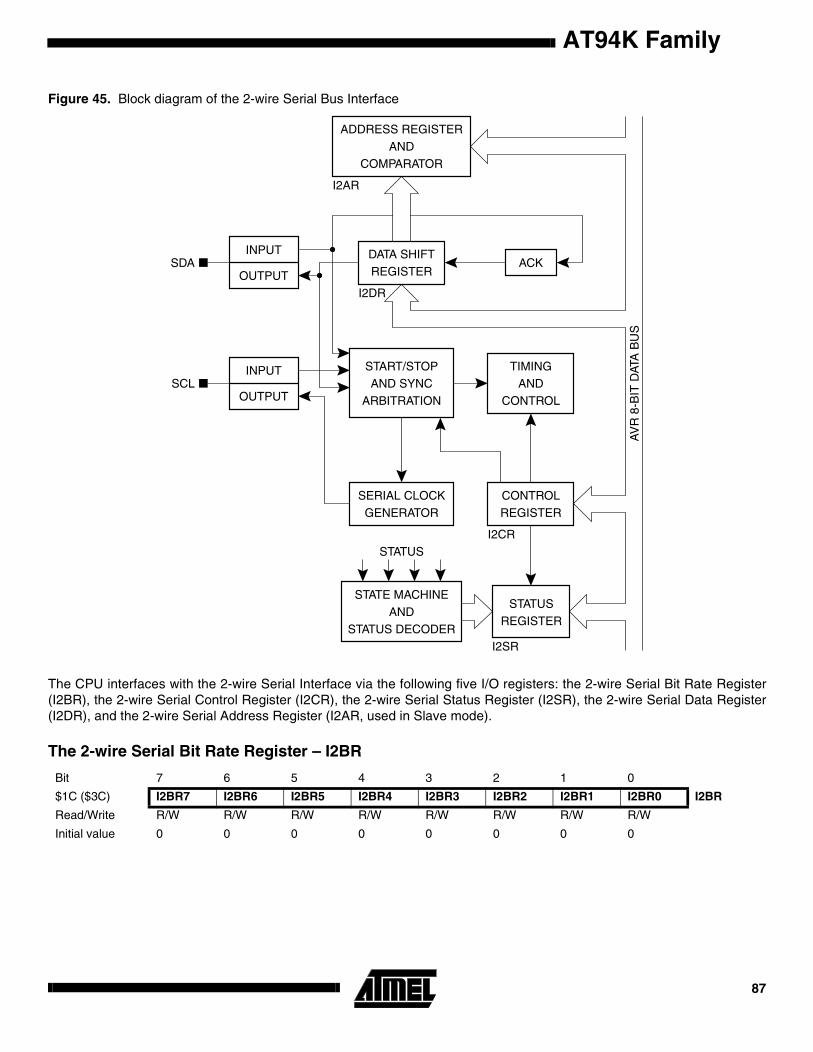
AT94K Family
Figure 45. Block diagram of the 2-wire Serial Bus Interface
The CPU interfaces with the 2-wire Serial Interface via the following five I/O registers: the 2-wire Serial Bit Rate Register(I2BR), the 2-wire Serial Control Register (I2CR), the 2-wire Serial Status Register (I2SR), the 2-wire Serial Data Register(I2DR), and the 2-wire Serial Address Register (I2AR, used in Slave mode).
The 2-wire Serial Bit Rate Register – I2BR
Bit 7 6 5 4 3 2 1 0
$1C ($3C) I2BR7 I2BR6 I2BR5 I2BR4 I2BR3 I2BR2 I2BR1 I2BR0 I2BR
Read/Write R/W R/W R/W R/W R/W R/W R/W R/W
Initial value 0 0 0 0 0 0 0 0
ACKINPUT
OUTPUT
INPUT
OUTPUT
START/STOPAND SYNC
ARBITRATION
TIMINGAND
CONTROL
SERIAL CLOCKGENERATOR
STATE MACHINEAND
STATUS DECODER
DATA SHIFTREGISTER
ADDRESS REGISTERAND
COMPARATOR
I2AR
SDA
SCL
I2DR
CONTROLREGISTER
STATUSREGISTER
STATUSI2CR
I2SRA
VR
8-B
IT D
ATA
BU
S
87

• Bits 7..0 - 2-wire Serial Bit Rate Register
I2BR selects the division factor for the bit rate generator. The bit rate generator is a frequency divider which generates theSCL clock frequency in the Master modes according to the following equation:
• Bit Rate = SCL frequency
• fCK = CPU Clock frequency
• I2BR = Contents of the 2-wire Serial Bit Rate Register
Note: Both the receiver and the transmitter can stretch the low period of the SCL line when waiting for user response, thereby reduc-ing the average bit rate.
The 2-wire Serial Control Register – I2CR
• Bit 7 - I2INT: 2-wire Serial Interrupt Flag
This bit is set by hardware when the 2-wire Serial Interface has finished its current job and expects application softwareresponse. If the I-bit in the SREG and I2IE in the I2CR register are set (one), the MCU will jump to the interrupt vector ataddress $011. While the I2INT flag is set, the bus SCL clock line low period is stretched. The I2INT flag must be cleared bysoftware by writing a logic one to it. Note that this flag is not automatically cleared by hardware when executing the interruptroutine. Also note that clearing this flag starts the operation of the 2-wire Serial Interface, so all accesses to the 2-wireSerial Address Register – I2AR, 2-wire Serial Status Register – I2SR, and 2-wire Serial Data Register – I2DR must be com-plete before clearing this flag.
• Bit 6 - I2EA: 2-wire Serial Enable Acknowledge Flag
I2EA flag controls the generation of the acknowledge pulse. If the I2EA bit is set, the ACK pulse is generated on the 2-wireSerial Bus if the following conditions are met:
1. The device’s own Slave address has been detected
2. A general call has been received, while the I2GCE bit in the I2AR is set
3. A data byte has been received in Master Receiver or Slave receiver mode
By setting the I2EA bit low the device can be virtually disconnected from the 2-wire Serial Bus temporarily. Address recog-nition can then be resumed by setting the I2EA bit again.
• Bit 5 - I2STA: 2-wire Serial Bus START Condition Flag
The I2STA flag is set by the CPU when it desires to become a Master on the 2-wire Serial Bus. The 2-wire serial hardwarechecks if the bus is available, and generates a Start condition on the bus if it is free. However, if the bus is not free, the 2-wire Serial Interface waits until a STOP condition is detected, and then generates a new Start condition to claim the busMaster status.
• Bit 4 - I2STO: 2-wire Serial Bus STOP Condition Flag
I2STO is a stop condition flag. In Master mode setting the I2STO bit in the control register will generate a STOP conditionon the 2-wire Serial Bus. When the STOP condition is executed on the bus, the I2STO bit is cleared automatically. In Slavemode setting the I2STO bit can be used to recover from an error condition. No stop condition is generated on the bus then,but the 2-wire Serial Interface returns to a well-defined unaddressed Slave mode.
• Bit 3 - I2WC: 2-wire Serial Write Collision Flag
Set when attempting to write to the 2-wire Serial Data Register – I2DR when I2INT is low. This flag is updated at eachattempt to write the I2DR register.
Bit 7 6 5 4 3 2 1 0
$36 ($56) I2INT I2EA I2STA I2STO I2WC I2EN - I2IE I2CR
Read/Write R/W R/W R/W R/W R R/W R R/W
Initial value 0 0 0 0 0 0 0 0
Bit RatefCK
16 + 2(I2BR)----------------------------------=
AT94K Family88

AT94K Family
• Bit 2 - I2EN: 2-wire Serial Interface Enable Flag
The I2EN bit enables 2-wire serial operation. If this flag is cleared (zero), the bus outputs SDA and SCL are set to highimpedance state, and the input signals are ignored. The interface is activated by setting this flag (one).
• Bit 1 - Res: Reserved Bit
This bit is a reserved bit in the ATmega83/163 and will always read as zero.
• Bit 0 - I2IE: 2-wire Serial Interrupt Enable
When this bit is enabled, and the I-bit in SREG is set, the 2-wire Serial Interrupt will be activated for as long as the I2INTflag is high.
The I2CR is used to control the operation of the 2-wire Serial Interface. It is used to enable the 2-wire Serial Interface, to ini-tiate a Master access, to generate a receiver acknowledge, to generate a stop condition, and control halting of the buswhile the data to be written to the bus are written to the I2DR. It also indicates a write collision if data is attempted written toI2DR while the register is inaccessible.
The 2-wire Serial Status Register – I2SR
• Bits 7..3 - I2S: 2-wire Serial Status
These 5 bits reflect the status of the 2-wire Serial Logic and the 2-wire Serial Bus.
• Bits 2..0 - Res: Reserved Bits
These bits are reserved in ATmega83/163 and will always read as zero
The I2SR is read only. It contains a status code which reflects the status of the 2-wire Serial Logic and the 2-wire SerialBus. There are 26 possible status codes. When I2SR contains $F8, no relevant state information is available and no 2-wireSerial Interrupt is requested. A valid status code is available in I2SR one CPU clock cycle after the 2-wire Serial Interruptflag (I2INT) is set by hardware and is valid until one CPU clock cycle after I2INT is cleared by software. Table 23 to Table27 give the status information for the various modes.
The 2-wire Serial Data Register – I2DR
• Bits 7..0 - I2D: 2-wire Serial Data Register
These eight bits constitute the next data byte to be transmitted, or the latest data byte received on the 2-wire Serial Bus.
In transmit mode, I2DR contains the next byte to be transmitted. In receive mode, the I2DR contains the last byte received.It is writable while the 2-wire Serial Interface is not in the process of shifting a byte. This occurs when the 2-wire SerialInterrupt flag (I2INT) is set by hardware. Note that the data register cannot be initialized by the user before the first interruptoccurs. The data in I2DR remain stable as long as I2INT is set. While data is shifted out, data on the bus is simultaneouslyshifted in. I2DR always contains the last byte present on the bus, except after a wake up from Power Down Mode, or PowerSave Mode by the 2-wire Serial Interrupt. For example, in the case of the lost bus arbitration, no data is lost in the transitionfrom Master-to-Slave. Receiving the ACK flag is controlled by the 2-wire Serial Logic automatically, the CPU cannot accessthe ACK bit directly.
Bit 7 6 5 4 3 2 1 0
$1D ($3D) I2S7 I2S6 I2S5 I2S4 I2S3 - - - I2SR
Read/Write R R R R R R R R
Initial value 1 1 1 1 1 0 0 0
Bit 7 6 5 4 3 2 1 0
$1F ($3F) I2D7 I2D6 I2D5 I2D4 I2D3 I2D2 I2D1 I2D0 I2DR
Read/Write R/W R/W R/W R/W R/W R/W R/W R/W
Initial value 1 1 1 1 1 1 1 1
89

The 2-wire Serial (Slave)Address Register – I2AR
• Bits 7..1 - I2A: 2-wire Serial Slave Address Register
These seven bits constitute the Slave address of the 2-wire Serial Bus interface unit.
• Bit 0 - I2GCE: 2-wire Serial General Call Recognition Enable Bit
This bit enables, if set, the recognition of the General Call given over the 2-wire Serial Bus.
The I2AR should be loaded with the 7-bit Slave address (in the seven most significant bits of I2AR) to which the 2-wireSerial Interface will respond when programmed as a Slave transmitter or receiver, and not needed in the Master modes.The LSB of I2AR is used to enable recognition of the general call address ($00). There is an associated address compara-tor that looks for the Slave address (or general call address if enabled) in the received serial address. If a match is found,an interrupt request is generated.
2-wire Serial ModesThe 2-wire Serial Interface can operate in four different modes:• Master Transmitter
• Master Receiver
• Slave Receiver
• Slave Transmitter
Data transfer in each mode of operation is shown in Figure 46 to Figure 49. These figures contain the followingabbreviations:
S: START condition
R: Read bit (high level at SDA)
W: Write bit (low level at SDA)
A: Acknowledge bit (low level at SDA)
A: Not acknowledge bit (high level at SDA)
Data: 8-bit data byte
P: STOP condition
In Figure 46 to Figure 49, circles are used to indicate that the 2-wire Serial Interrupt flag is set. The numbers in the circlesshow the status code held in I2SR. At these points, an interrupt routine must be executed to continue or complete the 2-wire Serial Transfer. The 2-wire Serial Transfer is suspended until the 2-wire Serial Interrupt flag is cleared by software.
The 2-wire Serial Interrupt flag is not automatically cleared by hardware when executing the interrupt routine. Also note thatthe 2-wire Serial Interface starts execution as soon as this bit is cleared, so that all access to I2AR, I2DR, and I2SR musthave been completed before clearing this flag.
When the 2-wire Serial Interrupt flag is set, the status code in I2SR is used to determine the appropriate software action.For each status code, the required software action and details of the following serial transfer are given in Table 23 to Table27.
Bit 7 6 5 4 3 2 1 0
$1E ($3E) I2A6 I2A5 I2A4 I2A3 I2A2 I2A1 I2A0 I2GCE I2AR
Read/Write R/W R/W R/W R/W R/W R/W R/W R/W
Initial value 1 1 1 1 1 1 1 0
AT94K Family90

AT94K Family
Master Transmitter ModeIn the Master Transmitter mode, a number of data bytes are transmitter to a Slave receiver (see Figure 46). Before MasterTransmitter mode can be entered, the I2CR must be initialized as follows:
I2EN must be set to enable the 2-wire Serial Interface, I2STA and I2STO must be cleared.
The Master Transmitter mode may now be entered by setting the I2STA bit. The 2-wire Serial Logic will now test the 2-wireSerial Bus and generate a START condition as soon as the bus becomes free. When a START condition is transmitted, the2-wire Serial Interrupt flag (I2INT) is set by hardware, and the status code in I2SR will be $08. I2DR must then be loadedwith the Slave address and the data direction bit (SLA+W). The I2INT flag must then be cleared by software before the 2-wire Serial Transfer can continue. The I2INT flag is cleared by writing a logic one to the flag.
When the Slave address and the direction bit have been transmitted and an acknowledgment bit has been received, I2INTis set again and a number of status codes in I2SR are possible. Status codes $18, $20, or $38 apply to Master mode, andstatus codes $68, $78, or $B0 apply to Slave mode. The appropriate action to be taken for each of these status codes isdetailed in Table 23. The data must be loaded when I2INT is high only. If not, the access will be discarded, and the WriteCollision bit – I2WC will be set in the I2CR register. This scheme is repeated until a STOP condition is transmitted by writ-ing a logic one to the I2STO bit in the I2CR register.
After a repeated START condition (state $10) the 2-wire Serial Interface may switch to the Master Receiver mode by load-ing I2DR with SLA+R.
Master Receiver ModeIn the Master Receiver mode, a number of data bytes are received from a Slave transmitter (see Figure 47). The transfer isinitialized as in the Master Transmitter mode. When the START condition has been transmitted, the I2INT flag is set byhardware. The software must then load I2DR with the 7-bit Slave address and the data direction bit (SLA+R). The 2-wireSerial Interrupt flag must then be cleared by software before the 2-wire Serial Transfer can continue.
When the Slave address and the direction bit have been transmitted and an acknowledgment bit has been received, I2INTis set again and a number of status codes in I2SR are possible. Status codes $40, $48, or $38 apply to Master mode, andstatus codes $68, $78, or $B0 apply to Slave mode. The appropriate action to be taken for each of these status codes isdetailed in Table 24. Received data can be read from the I2DR register when the I2INT flag is set high by hardware. Thisscheme is repeated until a STOP condition is transmitted by writing a logic one to the I2STO bit in the I2CR register.
After a repeated START condition (state $10), the 2-wire Serial Interface may switch to the Master Transmitter mode byloading I2DR with SLA+W.
Slave Receiver ModeIn the Slave Receiver mode, a number of data bytes are received from a Master Transmitter (see Figure 48). To initiate theSlave Receiver mode, I2AR and I2CR must be initialized as follows:
The upper 7 bits are the address to which the 2-wire Serial Interface will respond when addressed by a Master. If the LSBis set, the 2-wire Serial Interface will respond to the general call address ($00), otherwise it will ignore the general calladdress.
Table 20. I2CR: Master Transmitter Mode initialization
I2CR I2INT I2EA I2STA I2STO I2WC I2EN - I2IE
value 0 X 0 0 0 1 0 X
Table 21. I2AR: Slave Receiver Mode Initialization
I2AR I2A6 I2A5 I2A4 I2A3 I2A2 I2A1 I2A0 I2GCE
value Device’s own Slave address
91
I2EN must be set to enable the 2-wire Serial Interface. The I2EA bit must be set to enable the acknowledgment of thedevice’s own Slave address or the general call address. I2STA and I2STO must be cleared.
When I2AR and I2CR have been initialized, the 2-wire Serial Interface waits until it is addressed by its own Slave address(or the general call address if enabled) followed by the data direction bit which must be “0” (write) for the 2-wire Serial Inter-face to operate in the Slave Receiver mode. After its own Slave address and the write bit have been received, the 2-wireSerial Interrupt flag is set and a valid status code can be read from I2SR. The status code is used to determine the appro-priate software action. The appropriate action to be taken for each status code is detailed in Table 25. The Slave Receivermode may also be entered if arbitration is lost while the 2-wire Serial Interface is in the Master mode (see states $68 and$78).
If the I2EA bit is reset during a transfer, the 2-wire Serial Interface will return a “Not Acknowledged” (1) to SDA after thenext received data byte. While I2EA is reset, the 2-wire Serial Interface does not respond to its own Slave address. How-ever, the 2-wire Serial Bus is still monitored and address recognition may resume at any time by setting I2EA. This impliesthat the I2EA bit may be used to temporarily isolate the 2-wire Serial Interface from the 2-wire serial bus.
In ADC Noise Reduction Mode, Power Down Mode, and Power Save Mode, the clock system to the 2-wire Serial Interfaceis turned off. If the Slave Receiver mode is enabled, the interface can still acknowledge a general call and its own Slaveaddress by using the 2-wire serial bus clock as a clock source. The part will then wake up from sleep and the 2-wire SerialInterface will hold the SCL clock will low during the wake up and until the I2CINT flag is cleared.
Note that the 2-wire Serial Data Register – I2DR does not reflect the last byte present on the bus when waking up fromthese Sleep Modes.
Slave Transmitter ModeIn the Slave Transmitter mode, a number of data bytes are transmitted to a Master Receiver (see Figure 49). The transferis initialized as in the Slave Receiver mode. When I2AR and I2CR have been initialized, the 2-wire Serial Interface waitsuntil it is addressed by its own Slave address (or the general call address if enabled) followed by the data direction bit whichmust be “1” (read) for the 2-wire Serial Interface to operate in the Slave Transmitter mode. After its own Slave address andthe read bit have been received, the 2-wire Serial Interrupt flag is set and a valid status code can be read from I2SR. Thestatus code is used to determine the appropriate software action. The appropriate action to be taken for each status code isdetailed in Table 26. The Slave Transmitter mode may also be entered if arbitration is lost while the 2-wire Serial Interfaceis in the Master mode (see state $B0).
If the I2EA bit is reset during a transfer, the 2-wire Serial Interface will transmit the last byte of the transfer and enter state$C0 or state $C8. the 2-wire Serial Interface is switched to the not addressed Slave mode, and will ignore the Master if itcontinues the transfer. Thus the Master Receiver receives all “1” as serial data. While I2EA is reset, the 2-wire Serial Inter-face does not respond to its own Slave address. However, the 2-wire serial bus is still monitored and address recognitionmay resume at any time by setting I2EA. This implies that the I2EA bit may be used to temporarily isolate the 2-wire SerialInterface from the 2-wire serial bus.
Miscellaneous statesThere are two status codes that do not correspond to a defined 2-wire Serial Interface state, see Table 27.
Status $F8 indicates that no relevant information is available because the 2-wire Serial Interrup flag (I2INT) is not set yet.This occurs between other states, and when the 2-wire Serial Interface is not involved in a serial transfer.
Status $00 indicates that a bus error has occurred during a 2-wire serial transfer. A bus error occurs when a START orSTOP condition occurs at an illegal position in the format frame. Examples of such illegal positions are during the serialtransfer of an address byte, a data byte or an acknowledge bit. When a bus error occurs, I2INT is set. To recover from abus error, the I2STO flag must set and I2INT must be cleared by writing a logic one to it. This causes the 2-wire Serial Inter-face to enter the not addressed Slave mode and to clear the I2STO flag (no other bits in I2CR are affected). The SDA andSCL lines are released and no STOP condition is transmitted.
Table 22. I2CR: Slave Receiver Mode initialization
I2CR I2INT I2EA I2STA I2STO I2WC I2EN - I2IE
value 0 1 0 0 0 1 0 X
AT94K Family92
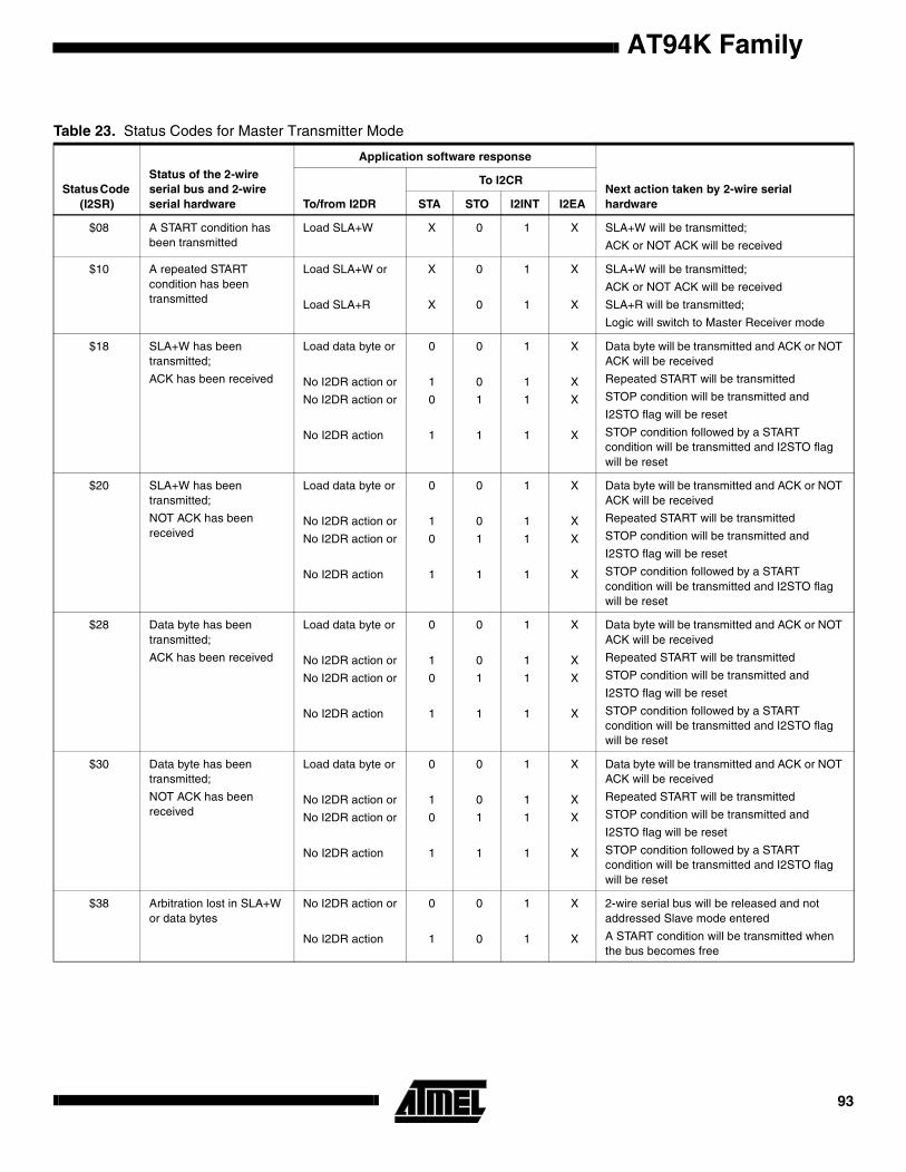
AT94K Family
Table 23. Status Codes for Master Transmitter Mode
Status Code (I2SR)
Status of the 2-wire serial bus and 2-wire serial hardware
Application software response
Next action taken by 2-wire serial hardwareTo/from I2DR
To I2CR
STA STO I2INT I2EA
$08 A START condition has been transmitted
Load SLA+W X 0 1 X SLA+W will be transmitted;
ACK or NOT ACK will be received
$10 A repeated START condition has been transmitted
Load SLA+W or
Load SLA+R
X
X
0
0
1
1
X
X
SLA+W will be transmitted;
ACK or NOT ACK will be received
SLA+R will be transmitted;
Logic will switch to Master Receiver mode
$18 SLA+W has been transmitted;
ACK has been received
Load data byte or
No I2DR action or
No I2DR action or
No I2DR action
0
1
0
1
0
0
1
1
1
1
1
1
X
X
X
X
Data byte will be transmitted and ACK or NOT ACK will be received
Repeated START will be transmitted
STOP condition will be transmitted and
I2STO flag will be reset
STOP condition followed by a START condition will be transmitted and I2STO flag will be reset
$20 SLA+W has been transmitted;
NOT ACK has been received
Load data byte or
No I2DR action or
No I2DR action or
No I2DR action
0
1
0
1
0
0
1
1
1
1
1
1
X
X
X
X
Data byte will be transmitted and ACK or NOT ACK will be received
Repeated START will be transmitted
STOP condition will be transmitted and
I2STO flag will be reset
STOP condition followed by a START condition will be transmitted and I2STO flag will be reset
$28 Data byte has been transmitted;
ACK has been received
Load data byte or
No I2DR action or
No I2DR action or
No I2DR action
0
1
0
1
0
0
1
1
1
1
1
1
X
X
X
X
Data byte will be transmitted and ACK or NOT ACK will be received
Repeated START will be transmitted
STOP condition will be transmitted and
I2STO flag will be reset
STOP condition followed by a START condition will be transmitted and I2STO flag will be reset
$30 Data byte has been transmitted;
NOT ACK has been received
Load data byte or
No I2DR action or
No I2DR action or
No I2DR action
0
1
0
1
0
0
1
1
1
1
1
1
X
X
X
X
Data byte will be transmitted and ACK or NOT ACK will be received
Repeated START will be transmitted
STOP condition will be transmitted and
I2STO flag will be reset
STOP condition followed by a START condition will be transmitted and I2STO flag will be reset
$38 Arbitration lost in SLA+W or data bytes
No I2DR action or
No I2DR action
0
1
0
0
1
1
X
X
2-wire serial bus will be released and not addressed Slave mode entered
A START condition will be transmitted when the bus becomes free
93

Figure 46. Formats and States in the Master Transmitter Mode
S SLA W A DATA A P
$08 $18 $28
S SLA W
$10
A P
$20
P
$30
A or A
$38
A
Other mastercontinues A or A
$38
Other mastercontinues
R
A
$68
Other mastercontinues
$78 $B0To correspondingstates in slave mode
MT
MR
Successfulltransmissionto a slavereceiver
Next transferstarted with arepeated startcondition
Not acknowledgereceived after theslave address
Not acknowledgereceived after a databyte
Arbitration lost in slaveaddress or data byte
Arbitration lost andaddressed as slave
DATA A
n
From master to slave
From slave to master
Any number of data bytesand their associated acknowledge bits
This number (contained in I2SR) correspondsto a defined state of the I2C bus
AT94K Family94
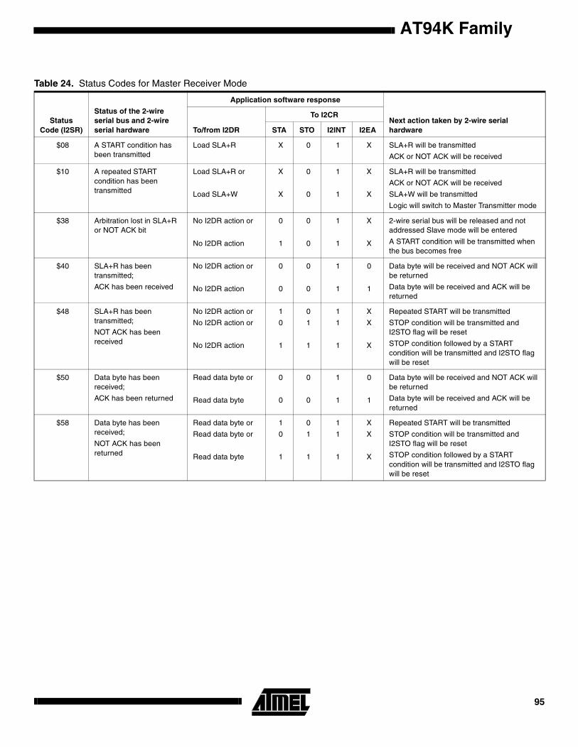
AT94K Family
Table 24. Status Codes for Master Receiver Mode
Status Code (I2SR)
Status of the 2-wire serial bus and 2-wire serial hardware
Application software response
Next action taken by 2-wire serial hardwareTo/from I2DR
To I2CR
STA STO I2INT I2EA
$08 A START condition has been transmitted
Load SLA+R X 0 1 X SLA+R will be transmitted
ACK or NOT ACK will be received
$10 A repeated START condition has been transmitted
Load SLA+R or
Load SLA+W
X
X
0
0
1
1
X
X
SLA+R will be transmitted
ACK or NOT ACK will be received
SLA+W will be transmitted
Logic will switch to Master Transmitter mode
$38 Arbitration lost in SLA+R or NOT ACK bit
No I2DR action or
No I2DR action
0
1
0
0
1
1
X
X
2-wire serial bus will be released and not addressed Slave mode will be entered
A START condition will be transmitted when the bus becomes free
$40 SLA+R has been transmitted;
ACK has been received
No I2DR action or
No I2DR action
0
0
0
0
1
1
0
1
Data byte will be received and NOT ACK will be returned
Data byte will be received and ACK will be returned
$48 SLA+R has been transmitted;
NOT ACK has been received
No I2DR action or
No I2DR action or
No I2DR action
1
0
1
0
1
1
1
1
1
X
X
X
Repeated START will be transmitted
STOP condition will be transmitted and I2STO flag will be reset
STOP condition followed by a START condition will be transmitted and I2STO flag will be reset
$50 Data byte has been received;
ACK has been returned
Read data byte or
Read data byte
0
0
0
0
1
1
0
1
Data byte will be received and NOT ACK will be returned
Data byte will be received and ACK will be returned
$58 Data byte has been received;
NOT ACK has been returned
Read data byte or
Read data byte or
Read data byte
1
0
1
0
1
1
1
1
1
X
X
X
Repeated START will be transmitted
STOP condition will be transmitted and I2STO flag will be reset
STOP condition followed by a START condition will be transmitted and I2STO flag will be reset
95
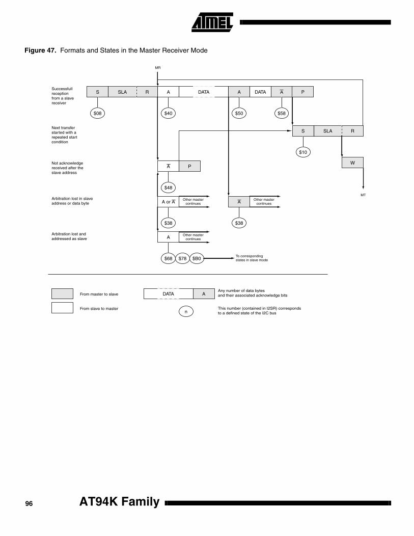
Figure 47. Formats and States in the Master Receiver Mode
S SLA R A DATA A
$08 $40 $50
S SLA R
$10
A P
$48
A or A
$38
Other mastercontinues
$38
Other mastercontinues
W
A
$68
Other mastercontinues
$78 $B0To correspondingstates in slave mode
MR
MT
Successfullreceptionfrom a slavereceiver
Next transferstarted with arepeated startcondition
Not acknowledgereceived after theslave address
Arbitration lost in slaveaddress or data byte
Arbitration lost andaddressed as slave
DATA A
n
From master to slave
From slave to master
Any number of data bytesand their associated acknowledge bits
This number (contained in I2SR) correspondsto a defined state of the I2C bus
PDATA A
$58
A
AT94K Family96

AT94K Family
Table 25. Status Codes for Slave Receiver Mode
Status Code (I2SR)
Status of the 2-wire serial bus and 2-wire serial hardware
Application software response
Next action taken by 2-wire serial hardwareTo/from I2DR
To I2CR
STA STO I2INT I2EA
$60 Own SLA+W has been received;
ACK has been returned
No I2DR action or
No I2DR action
X
X
0
0
1
1
0
1
Data byte will be received and NOT ACK will be returned
Data byte will be received and ACK will be returned
$68 Arbitration lost in SLA+R/W as Master; own SLA+W has been received;
ACK has been returned
No I2DR action or
No I2DR action
X
X
0
0
1
1
0
1
Data byte will be received and NOT ACK will be returned
Data byte will be received and ACK will be returned
$70 General call address has been received;
ACK has been returned
No I2DR action or
No I2DR action
X
X
0
0
1
1
0
1
Data byte will be received and NOT ACK will be returned
Data byte will be received and ACK will be returned
$78 Arbitration lost in SLA+R/W as Master; General call address has been received;
ACK has been returned
No I2DR action or
No I2DR action
X
X
0
0
1
1
0
1
Data byte will be received and NOT ACK will be returned
Data byte will be received and ACK will be returned
$80 Previously addressed with own SLA+W; data has been received;
ACK has been returned
No I2DR action or
No I2DR action
X
X
0
0
1
1
0
1
Data byte will be received and NOT ACK will be returned
Data byte will be received and ACK will be returned
$88 Previously addressed with own SLA+W; data has been received;
NOT ACK has been returned
Read data byte or
Read data byte or
Read data byte or
Read data byte
0
0
1
1
0
0
0
0
1
1
1
1
0
1
0
1
Switched to the not addressed Slave mode;
no recognition of own SLA or GCA
Switched to the not addressed Slave mode;
own SLA will be recognized;
GCA will be recognized if GC = “1”
Switched to the not addressed Slave mode;
no recognition of own SLA or GCA;
a START condition will be transmitted when the bus becomes free
Switched to the not addressed Slave mode;
own SLA will be recognized;
GCA will be recognized if GC = “1”;
a START condition will be transmitted when the bus becomes free
97
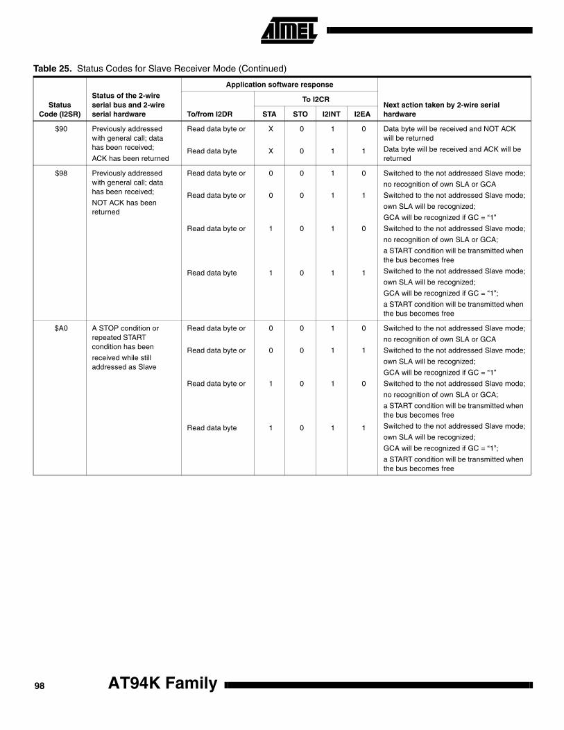
$90 Previously addressed with general call; data has been received;
ACK has been returned
Read data byte or
Read data byte
X
X
0
0
1
1
0
1
Data byte will be received and NOT ACK will be returned
Data byte will be received and ACK will be returned
$98 Previously addressed with general call; data has been received;
NOT ACK has been returned
Read data byte or
Read data byte or
Read data byte or
Read data byte
0
0
1
1
0
0
0
0
1
1
1
1
0
1
0
1
Switched to the not addressed Slave mode;
no recognition of own SLA or GCA
Switched to the not addressed Slave mode;
own SLA will be recognized;
GCA will be recognized if GC = “1”
Switched to the not addressed Slave mode;
no recognition of own SLA or GCA;
a START condition will be transmitted when the bus becomes free
Switched to the not addressed Slave mode;
own SLA will be recognized;
GCA will be recognized if GC = “1”;
a START condition will be transmitted when the bus becomes free
$A0 A STOP condition or repeated START condition has been
received while still addressed as Slave
Read data byte or
Read data byte or
Read data byte or
Read data byte
0
0
1
1
0
0
0
0
1
1
1
1
0
1
0
1
Switched to the not addressed Slave mode;
no recognition of own SLA or GCA
Switched to the not addressed Slave mode;
own SLA will be recognized;
GCA will be recognized if GC = “1”
Switched to the not addressed Slave mode;
no recognition of own SLA or GCA;
a START condition will be transmitted when the bus becomes free
Switched to the not addressed Slave mode;
own SLA will be recognized;
GCA will be recognized if GC = “1”;
a START condition will be transmitted when the bus becomes free
Table 25. Status Codes for Slave Receiver Mode (Continued)
Status Code (I2SR)
Status of the 2-wire serial bus and 2-wire serial hardware
Application software response
Next action taken by 2-wire serial hardwareTo/from I2DR
To I2CR
STA STO I2INT I2EA
AT94K Family98

AT94K Family
Figure 48. Formats and States in the Slave Receiver Mode
S SLA W A DATA A
$60 $80
$88
A
$68
Reception of the ownslave address and one ormore data bytes. All areacknowledged
Last data byte receivedis not acknowledged
Arbitration lost as masterand addressed as slave
Reception of the general calladdress and one or more databytes
Last data byte received isnot acknowledged
n
From master to slave
From slave to master
Any number of data bytesand their associated acknowledge bits
This number (contained in I2SR) correspondsto a defined state of the I2C bus
P or SDATA A
$80 $A0
P or SA
A DATA A
$70 $90
$98
A
$78
P or SDATA A
$90 $A0
P or SA
General Call
Arbitration lost as master andaddressed as slave by general call
DATA A
99
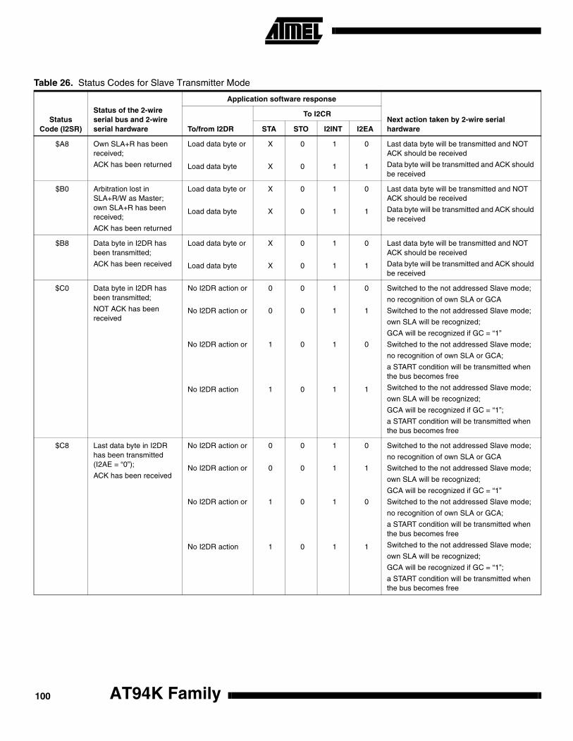
Table 26. Status Codes for Slave Transmitter Mode
Status Code (I2SR)
Status of the 2-wire serial bus and 2-wire serial hardware
Application software response
Next action taken by 2-wire serial hardwareTo/from I2DR
To I2CR
STA STO I2INT I2EA
$A8 Own SLA+R has been received;
ACK has been returned
Load data byte or
Load data byte
X
X
0
0
1
1
0
1
Last data byte will be transmitted and NOT ACK should be received
Data byte will be transmitted and ACK should be received
$B0 Arbitration lost in SLA+R/W as Master; own SLA+R has been received;
ACK has been returned
Load data byte or
Load data byte
X
X
0
0
1
1
0
1
Last data byte will be transmitted and NOT ACK should be received
Data byte will be transmitted and ACK should be received
$B8 Data byte in I2DR has been transmitted;
ACK has been received
Load data byte or
Load data byte
X
X
0
0
1
1
0
1
Last data byte will be transmitted and NOT ACK should be received
Data byte will be transmitted and ACK should be received
$C0 Data byte in I2DR has been transmitted;
NOT ACK has been received
No I2DR action or
No I2DR action or
No I2DR action or
No I2DR action
0
0
1
1
0
0
0
0
1
1
1
1
0
1
0
1
Switched to the not addressed Slave mode;
no recognition of own SLA or GCA
Switched to the not addressed Slave mode;
own SLA will be recognized;
GCA will be recognized if GC = “1”
Switched to the not addressed Slave mode;
no recognition of own SLA or GCA;
a START condition will be transmitted when the bus becomes free
Switched to the not addressed Slave mode;
own SLA will be recognized;
GCA will be recognized if GC = “1”;
a START condition will be transmitted when the bus becomes free
$C8 Last data byte in I2DR has been transmitted (I2AE = “0”);
ACK has been received
No I2DR action or
No I2DR action or
No I2DR action or
No I2DR action
0
0
1
1
0
0
0
0
1
1
1
1
0
1
0
1
Switched to the not addressed Slave mode;
no recognition of own SLA or GCA
Switched to the not addressed Slave mode;
own SLA will be recognized;
GCA will be recognized if GC = “1”
Switched to the not addressed Slave mode;
no recognition of own SLA or GCA;
a START condition will be transmitted when the bus becomes free
Switched to the not addressed Slave mode;
own SLA will be recognized;
GCA will be recognized if GC = “1”;
a START condition will be transmitted when the bus becomes free
AT94K Family100
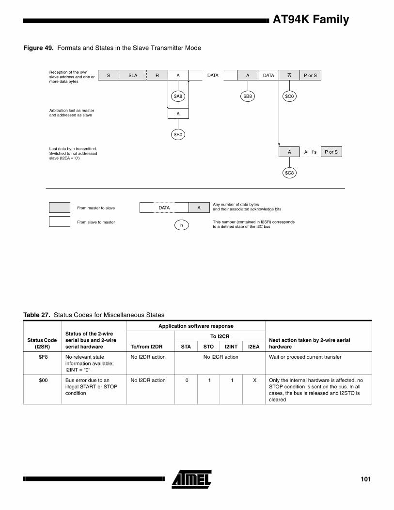
AT94K Family
Figure 49. Formats and States in the Slave Transmitter Mode
Table 27. Status Codes for Miscellaneous States
Status Code (I2SR)
Status of the 2-wire serial bus and 2-wire serial hardware
Application software response
Next action taken by 2-wire serial hardwareTo/from I2DR
To I2CR
STA STO I2INT I2EA
$F8 No relevant state information available; I2INT = “0”
No I2DR action No I2CR action Wait or proceed current transfer
$00 Bus error due to an illegal START or STOP condition
No I2DR action 0 1 1 X Only the internal hardware is affected, no STOP condition is sent on the bus. In all cases, the bus is released and I2STO is cleared
S SLA R A DATA A
$A8 $B8
A
$B0
Reception of the ownslave address and one ormore data bytes
Last data byte transmitted.Switched to not addressedslave (I2EA = '0')
Arbitration lost as masterand addressed as slave
n
From master to slave
From slave to master
Any number of data bytesand their associated acknowledge bits
This number (contained in I2SR) correspondsto a defined state of the I2C bus
P or SDATA
$C0
DATA A
A
$C8
P or SAll 1's
A
101

I/O-portsAll AVR ports have true read-modify-write functionality when used as general I/O ports. This means that the direction ofone port pin can be changed without unintentionally changing the direction of any other pin with the SBI and CBI instruc-tions. The same applies for changing drive value (if configured as output) or enabling/disabling of pull-up resistors (ifconfigured as input).
Port DPort D is an 8-bit bi-directional I/O port with internal pull-up resistors.
Three I/O memory address locations are allocated for the Port D, one each for the Data Register – PORTD, $12($32), DataDirection Register – DDRD, $11($31) and the Port D Input Pins – PIND, $10($30). The Port D Input Pins address is readonly, while the Data Register and the Data Direction Register are read/write.
The Port D output buffers can sink 20 mA. As inputs, Port D pins that are externally pulled low will source current if the pull-up resistors are activated.
Port D Data Register – PORTD
Port D Data Direction Register – DDRD
Port D Input Pins Address – PIND
The Port D Input Pins address – PIND – is not a register, and this address enables access to the physical value on eachPort D pin. When reading PORTD, the Port D Data Latch is read, and when reading PIND, the logical values present on thepins are read.
Bit 7 6 5 4 3 2 1 0
$12 PORTD7 PORTD6 PORTD5 PORTD4 PORTD3 PORTD2 PORTD1 PORTD0 PORTD
Read/Write R/W R/W R/W R/W R/W R/W R/W R/W
Initial value 0 0 0 0 0 0 0 0
Bit 7 6 5 4 3 2 1 0
$11 DDD7 DDD6 DDD5 DDD4 DDD3 DDD2 DDD1 DDD0 DDRD
Read/Write R/W R/W R/W R/W R/W R/W R/W R/W
Initial value 0 0 0 0 0 0 0 0
Bit 7 6 5 4 3 2 1 0
$10 PIND7 PIND6 PIND5 PIND4 PIND3 PIND2 PIND1 PIND0 PIND
Read/Write R R R R R R R R
Initial value Hi-Z Hi-Z Hi-Z Hi-Z Hi-Z Hi-Z Hi-Z Hi-Z
AT94K Family102

AT94K Family
Port D as general digital I/O
PDn, General I/O pin: The DDDn bit in the DDRD register selects the direction of this pin. If DDDn is set (one), PDn is con-figured as an output pin. If DDDn is cleared (zero), PDn is configured as an input pin. If PDn is set (one) when configuredas an input pin the MOS pull up resistor is activated. To switch the pull up resistor off the PDn has to be cleared (zero) orthe pin has to be configured as an output pin. The port pins are tri-stated when a reset condition becomes active, even ifthe clock is not running.
Note: n: 7,6...0, pin number
Figure 50. Port D Schematic Diagram (Pins PD0)
Table 28. DDDn Bits on Port D Pins
DDDn PORTDn I/O Pull-up Comment
0 0 Input No Tri-state (Hi-Z)
0 1 Input Yes PDn will source current if external pulled low
1 0 Output No Push-pull Zero Output
1 1 Output No Push-pull One Output
PD* DA
TA
BU
SRL
WL
DDD*Q D
R
PORTD*Q D
R
RESET
RESET
WD
RD
RP
GTS
DL
MOSPULLUP
RESETDL
GTS: Global Tri-StateDL: Configuration DownloadWL: Write PORTDWD: Write DDRDRL: Read PORTD LatchRD: Read DDRDRP: Read PORTD Pin
103

Port E
Port E is an 8-bit bi-directional I/O port with internal pull-up resistors.
Three I/O memory address locations are allocated for the Port E, one each for the Data Register – PORTE, $03($23), DataDirection Register – DDRE, $02($22) and the Port E Input Pins – PINE, $01($21). The Port E Input Pins address is readonly, while the Data Register and the Data Direction Register are read/write.
The Port E output buffers can sink 20 mA. As inputs, Port E pins that are externally pulled low will source current if the pull-up resistors are activated.
All Port E pins have alternate functions as shown in the following table:
When the pins are used for the alternate function the DDRE and PORTE register has to be set according to the alternatefunction description.
Port E Data Register – PORTE
Port E Data Direction Register – DDRE
Port E Input Pins Address – PINE
The Port E Input Pins address – PINE – is not a register, and this address enables access to the physical value on eachPort E pin. When reading PORTE, the Port E Data Latch is read, and when reading PINE, the logical values present on thepins are read.
Table 29. Port E Pins Alternate Functions Controlled by ACR and AVR I/O Registers
Port Pin Alternate Function Input Output
PE1 RX0 (UART0 Receive Pin) - Output Compare Timer0/PWM0
PE0 TX0 (UART0 Transmit Pin) External Timer0 Clock -
PE3 RX1 (UART1 Receive Pin) - Output Compare Timer2/PWM2
PE2 TX1 (UART1 Transmit Pin) - -
PE4 INT4 (External Interrupt4 Input)External Timer1 Clock
-
PE5 INT5 (External Interrupt5 Input) - Output Compare Timer1B/PWM1B
PE6 INT6 (External Interrupt6 Input) - Output Compare Timer1A/PWM1A
PE7 INT7 (External Interrupt7 Input) Input Capture Counter1
Bit 7 6 5 4 3 2 1 0
$03 ($23) PORTE7 PORTE6 PORTE5 PORTE4 PORTE3 PORTE2 PORTE1 PORTE0 PORTE
Read/Write R/W R/W R/W R/W R/W R/W R/W R/W
Initial value 0 0 0 0 0 0 0 0
Bit 7 6 5 4 3 2 1 0
$02 ($22) DDE7 DDE6 DDE5 DDE4 DDE3 DDE2 DDE1 DDE0 DDRE
Read/Write R/W R/W R/W R/W R/W R/W R/W R/W
Initial value 0 0 0 0 0 0 0 0
Bit 7 6 5 4 3 2 1 0
$01 ($21) PINE7 PINE6 PINE5 PINE4 PINE3 PINE2 PINE1 PINE0 PINE
Read/Write R R R R R R R R
Initial value Hi-Z Hi-Z Hi-Z Hi-Z Hi-Z Hi-Z Hi-Z Hi-Z
AT94K Family104
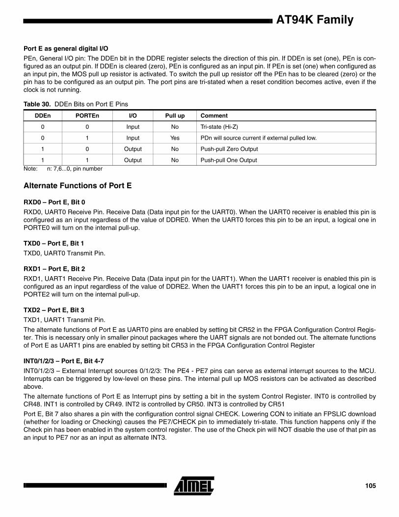
AT94K Family
Port E as general digital I/O
PEn, General I/O pin: The DDEn bit in the DDRE register selects the direction of this pin. If DDEn is set (one), PEn is con-figured as an output pin. If DDEn is cleared (zero), PEn is configured as an input pin. If PEn is set (one) when configured asan input pin, the MOS pull up resistor is activated. To switch the pull up resistor off the PEn has to be cleared (zero) or thepin has to be configured as an output pin. The port pins are tri-stated when a reset condition becomes active, even if theclock is not running.
Note: n: 7,6...0, pin number
Alternate Functions of Port E
RXD0 – Port E, Bit 0
RXD0, UART0 Receive Pin. Receive Data (Data input pin for the UART0). When the UART0 receiver is enabled this pin isconfigured as an input regardless of the value of DDRE0. When the UART0 forces this pin to be an input, a logical one inPORTE0 will turn on the internal pull-up.
TXD0 – Port E, Bit 1
TXD0, UART0 Transmit Pin.
RXD1 – Port E, Bit 2
RXD1, UART1 Receive Pin. Receive Data (Data input pin for the UART1). When the UART1 receiver is enabled this pin isconfigured as an input regardless of the value of DDRE2. When the UART1 forces this pin to be an input, a logical one inPORTE2 will turn on the internal pull-up.
TXD2 – Port E, Bit 3
TXD1, UART1 Transmit Pin.
The alternate functions of Port E as UART0 pins are enabled by setting bit CR52 in the FPGA Configuration Control Regis-ter. This is necessary only in smaller pinout packages where the UART signals are not bonded out. The alternate functionsof Port E as UART1 pins are enabled by setting bit CR53 in the FPGA Configuration Control Register
INT0/1/2/3 – Port E, Bit 4-7
INT0/1/2/3 – External Interrupt sources 0/1/2/3: The PE4 - PE7 pins can serve as external interrupt sources to the MCU.Interrupts can be triggered by low-level on these pins. The internal pull up MOS resistors can be activated as describedabove.
The alternate functions of Port E as Interrupt pins by setting a bit in the system Control Register. INT0 is controlled byCR48. INT1 is controlled by CR49. INT2 is controlled by CR50. INT3 is controlled by CR51
Port E, Bit 7 also shares a pin with the configuration control signal CHECK. Lowering CON to initiate an FPSLIC download(whether for loading or Checking) causes the PE7/CHECK pin to immediately tri-state. This function happens only if theCheck pin has been enabled in the system control register. The use of the Check pin will NOT disable the use of that pin asan input to PE7 nor as an input as alternate INT3.
Table 30. DDEn Bits on Port E Pins
DDEn PORTEn I/O Pull up Comment
0 0 Input No Tri-state (Hi-Z)
0 1 Input Yes PDn will source current if external pulled low.
1 0 Output No Push-pull Zero Output
1 1 Output No Push-pull One Output
105
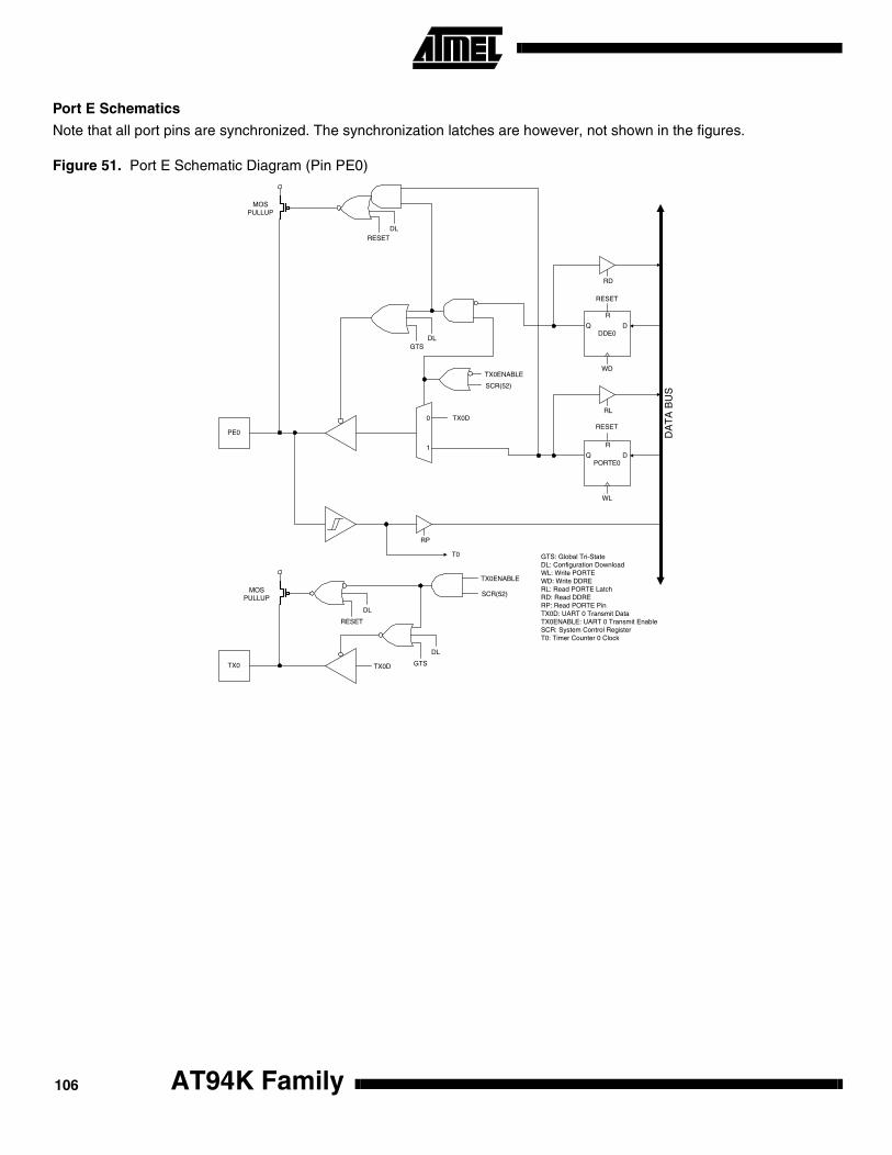
Port E Schematics
Note that all port pins are synchronized. The synchronization latches are however, not shown in the figures.
Figure 51. Port E Schematic Diagram (Pin PE0)
PE0
TX0D
DA
TA
BU
S
GTSDL
SCR(52)
MOSPULLUP
RL
WL
DDE0Q D
R
PORTE0Q D
R
RESET
RESET
WD
RD
RP
GTS: Global Tri-StateDL: Configuration DownloadWL: Write PORTEWD: Write DDRERL: Read PORTE LatchRD: Read DDRERP: Read PORTE PinTX0D: UART 0 Transmit DataTX0ENABLE: UART 0 Transmit EnableSCR: System Control RegisterT0: Timer Counter 0 Clock
1
0
T0
TX0
MOSPULLUP
TX0D
SCR(52)
TX0ENABLE
TX0ENABLE
RESETDL
DL
RESET
DL
GTS
AT94K Family106
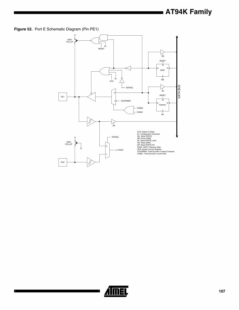
AT94K Family
Figure 52. Port E Schematic Diagram (Pin PE1)
PE1 DA
TA
BU
S
GTSDL
SCR(52)
RL
WL
DDE1Q D
R
PORTE1Q D
R
RESET
RESET
WD
RD
RP
GTS: Global Tri-StateDL: Configuration DownloadWL: Write PORTEWD: Write DDRERL: Read PORTE LatchRD: Read DDRERP: Read PORTE PinRX0D: UART 0 Receive DataSCR: System Control RegisterOC0/PMW0: Timer/Counter 0 Output CompareCOM0*: Timer/Counter 0 control bits
RX0
RX0D
SCR(52)
0
1
MOSPULLUP
OC0/PMW01
0
COM00
COM01
MOSPULLUP
RESETDL
107
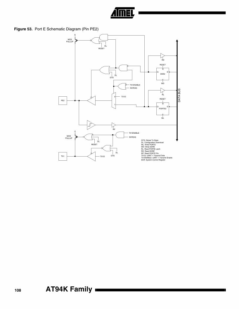
Figure 53. Port E Schematic Diagram (Pin PE2)
PE2 DA
TA
BU
S
RL
WL
DDE2Q D
R
PORTE2Q D
R
RESET
RESET
WD
RD
RP
GTS: Global Tri-StateDL: Configuration DownloadWL: Write PORTEWD: Write DDRERL: Read PORTE LatchRD: Read DDRERP: Read PORTE PinTX1D: UART 1 Transmit DataTX1ENABLE: UART 1 Transmit EnableSCR: System Control Register
TX1D
GTSDL
SCR(53)
1
0
TX1ENABLE
MOSPULLUP
RESETDL
TX1
MOSPULLUP
TX1D
SCR(53)
TX1ENABLE
DL
RESET
DL
GTS
AT94K Family108

AT94K Family
Figure 54. Port E Schematic Diagram (Pin PE3)
PE3 DA
TA
BU
S
GTSDL
SCR(53)
RL
WL
DDE3Q D
R
PORTE3Q D
R
RESET
RESET
WD
RD
RP
GTS: Global Tri-StateDL: Configuration DownloadWL: Write PORTEWD: Write DDRERL: Read PORTE LatchRD: Read DDRERP: Read PORTE PinRX1D: UART 1 Receive DataSCR: System Control RegisterOC2/PMW2: Timer/Counter 2 Output CompareCOM2*: Timer/Counter 2 control bitsRX1
RX1D
SCR(53)
0
1
MOSPULLUP
OC2/PMW21
0
COM20
COM21
MOSPULLUP
RESETDL
109

Figure 55. Port E Schematic Diagram (Pin PE4)
PE4 DA
TA
BU
S
GTSDL
SCR(48)
RL
DDE4Q D
R
RESET
WD
RD
RP
GTS: Global Tri-StateDL: Configuration DownloadWL: Write PORTEWD: Write DDRERL: Read PORTE LatchRD: Read DDRERP: Read PORTE Pinextintp0: External Interrupt 0SCR: System Control RegisterT1: Timer/Counter1 External clockINTP0
extintp0
SCR(48)
0
1
MOSPULLUP
WL
PORTE4Q D
R
RESET
T1
MOSPULLUP
RESETDL
AT94K Family110

AT94K Family
Figure 56. Port E Schematic Diagram (Pin PE5)
PE5 DA
TA
BU
S
GTSDL
SCR(49)
RL
DDE5Q D
R
RESET
WD
RD
RP
GTS: Global Tri-StateDL: Configuration DownloadWL: Write PORTEWD: Write DDRERL: Read PORTE LatchRD: Read DDRERP: Read PORTE Pinextintp1: External Interrupt 1SCR: System Control RegisterOC1B: Timer/Counter1 Output CompareBCOM1B*: Timer/Counter1 B control bits
INTP1
extintp1
SCR(49)
0
1
MOSPULLUP
WL
PORTE5Q D
R
RESET
OC1B
COM1B0
COM1B1
1
0
MOSPULLUP
RESETDL
111

Figure 57. Port E Schematic Diagram (Pin PE6)
PE6 DA
TA
BU
S
GTSDL
SCR(50)
RL
DDE6Q D
R
RESET
WD
RD
RP
GTS: Global Tri-StateDL: Configuration DownloadWL: Write PORTEWD: Write DDRERL: Read PORTE LatchRD: Read DDRERP: Read PORTE Pinextintp2: External Interrupt 2SCR: System Control RegisterOC1A: Timer/Counter1 Output Compare ACOM1A*: Timer/Counter1 A control bits
INTP2
extintp2
SCR(50)
0
1
MOSPULLUP
WL
PORTE6Q D
R
RESET
OC1A
COM1A0
COM1A1
1
0
MOSPULLUP
RESETDL
AT94K Family112

AT94K Family
Figure 58. Port E Schematic Diagram (Pin PE7)
PE7 DA
TA
BU
S
GTSDL
SCR(51)
RL
DDE7Q D
R
RESET
WD
RD
RP
GTS: Global Tri-StateDL: Configuration DownloadWL: Write PORTEWD: Write DDRERL: Read PORTE LatchRD: Read DDRERP: Read PORTE Pinextintp3: External Interrupt 3SCR: System Control RegisterICP: Timer/Counter Input Capture PinINTP3
extintp3
SCR(51)
0
1
MOSPULLUP
WL
PORTE7Q D
R
RESET
ICP
MOSPULLUP
RESETDL
113
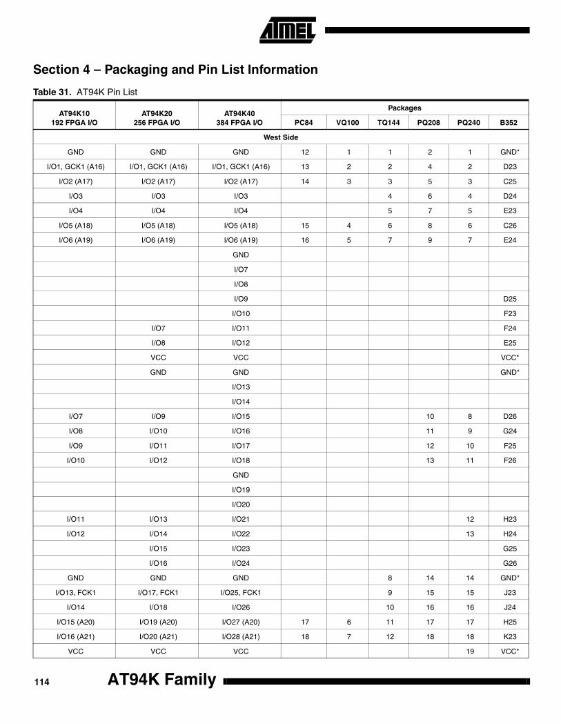
Section 4 – Packaging and Pin List Information
Table 31. AT94K Pin List
AT94K10192 FPGA I/O
AT94K20256 FPGA I/O
AT94K40384 FPGA I/O
Packages
PC84 VQ100 TQ144 PQ208 PQ240 B352
West Side
GND GND GND 12 1 1 2 1 GND*
I/O1, GCK1 (A16) I/O1, GCK1 (A16) I/O1, GCK1 (A16) 13 2 2 4 2 D23
I/O2 (A17) I/O2 (A17) I/O2 (A17) 14 3 3 5 3 C25
I/O3 I/O3 I/O3 4 6 4 D24
I/O4 I/O4 I/O4 5 7 5 E23
I/O5 (A18) I/O5 (A18) I/O5 (A18) 15 4 6 8 6 C26
I/O6 (A19) I/O6 (A19) I/O6 (A19) 16 5 7 9 7 E24
GND
I/O7
I/O8
I/O9 D25
I/O10 F23
I/O7 I/O11 F24
I/O8 I/O12 E25
VCC VCC VCC*
GND GND GND*
I/O13
I/O14
I/O7 I/O9 I/O15 10 8 D26
I/O8 I/O10 I/O16 11 9 G24
I/O9 I/O11 I/O17 12 10 F25
I/O10 I/O12 I/O18 13 11 F26
GND
I/O19
I/O20
I/O11 I/O13 I/O21 12 H23
I/O12 I/O14 I/O22 13 H24
I/O15 I/O23 G25
I/O16 I/O24 G26
GND GND GND 8 14 14 GND*
I/O13, FCK1 I/O17, FCK1 I/O25, FCK1 9 15 15 J23
I/O14 I/O18 I/O26 10 16 16 J24
I/O15 (A20) I/O19 (A20) I/O27 (A20) 17 6 11 17 17 H25
I/O16 (A21) I/O20 (A21) I/O28 (A21) 18 7 12 18 18 K23
VCC VCC VCC 19 VCC*
AT94K Family114
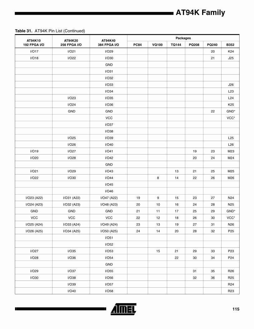
AT94K Family
I/O17 I/O21 I/O29 20 K24
I/O18 I/O22 I/O30 21 J25
GND
I/O31
I/O32
I/O33 J26
I/O34 L23
I/O23 I/O35 L24
I/O24 I/O36 K25
GND GND 22 GND*
VCC VCC*
I/O37
I/O38
I/O25 I/O39 L25
I/O26 I/O40 L26
I/O19 I/O27 I/O41 19 23 M23
I/O20 I/O28 I/O42 20 24 M24
GND
I/O21 I/O29 I/O43 13 21 25 M25
I/O22 I/O30 I/O44 8 14 22 26 M26
I/O45
I/O46
I/O23 (A22) I/O31 (A22) I/O47 (A22) 19 9 15 23 27 N24
I/O24 (A23) I/O32 (A23) I/O48 (A23) 20 10 16 24 28 N25
GND GND GND 21 11 17 25 29 GND*
VCC VCC VCC 22 12 18 26 30 VCC*
I/O25 (A24) I/O33 (A24) I/O49 (A24) 23 13 19 27 31 N26
I/O26 (A25) I/O34 (A25) I/O50 (A25) 24 14 20 28 32 P25
I/O51
I/O52
I/O27 I/O35 I/O53 15 21 29 33 P23
I/O28 I/O36 I/O54 22 30 34 P24
GND
I/O29 I/O37 I/O55 31 35 R26
I/O30 I/O38 I/O56 32 36 R25
I/O39 I/O57 R24
I/O40 I/O58 R23
Table 31. AT94K Pin List (Continued)
AT94K10192 FPGA I/O
AT94K20256 FPGA I/O
AT94K40384 FPGA I/O
Packages
PC84 VQ100 TQ144 PQ208 PQ240 B352
115
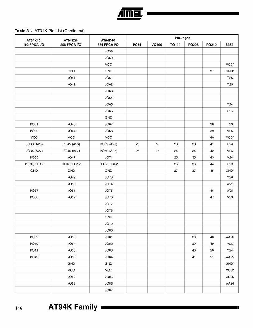
I/O59
I/O60
VCC VCC*
GND GND 37 GND*
I/O41 I/O61 T26
I/O42 I/O62 T25
I/O63
I/O64
I/O65 T24
I/O66 U25
GND
I/O31 I/O43 I/O67 38 T23
I/O32 I/O44 I/O68 39 V26
VCC VCC VCC 40 VCC*
I/O33 (A26) I/O45 (A26) I/O69 (A26) 25 16 23 33 41 U24
I/O34 (A27) I/O46 (A27) I/O70 (A27) 26 17 24 34 42 V25
I/O35 I/O47 I/O71 25 35 43 V24
I/O36, FCK2 I/O48, FCK2 I/O72, FCK2 26 36 44 U23
GND GND GND 27 37 45 GND*
I/O49 I/O73 Y26
I/O50 I/O74 W25
I/O37 I/O51 I/O75 46 W24
I/O38 I/O52 I/O76 47 V23
I/O77
I/O78
GND
I/O79
I/O80
I/O39 I/O53 I/O81 38 48 AA26
I/O40 I/O54 I/O82 39 49 Y25
I/O41 I/O55 I/O83 40 50 Y24
I/O42 I/O56 I/O84 41 51 AA25
GND GND GND*
VCC VCC VCC*
I/O57 I/O85 AB25
I/O58 I/O86 AA24
I/O87
Table 31. AT94K Pin List (Continued)
AT94K10192 FPGA I/O
AT94K20256 FPGA I/O
AT94K40384 FPGA I/O
Packages
PC84 VQ100 TQ144 PQ208 PQ240 B352
AT94K Family116

AT94K Family
I/O88
I/O43 (A28) I/O59 (A28) I/O89 (A28) 27 18 28 42 52 Y23
I/O44 I/O60 I/O90 19 29 43 53 AC26
GND
I/O91 AD26
I/O92 AC25
I/O45 I/O61 I/O93 30 44 54 AA23
I/O46 I/O62 I/O94 31 45 55 AB24
I/O47 (OTS) I/O63 (OTS) I/O95 (OTS) 28 20 32 46 56 AD25
I/O48, GCK2 (A29) I/O64, GCK2 (A29) I/O96, GCK2 (A29) 29 21 33 47 57 AC24
AVRRESET AVRRESET AVRRESET 30 22 34 48 58 AB23
GND GND GND 31 23 35 49 59 GND*
M0 M0 M0 32 24 36 50 60 AD24
South Side
VCC VCC VCC 33 25 37 55 61 VCC*
M2 M2 M2 34 26 38 56 62 AC23
I/O49, GCK3 I/O65, GCK3 I/O97, GCK3 35 27 39 57 63 AE24
I/O50 (HDC) I/O66 (HDC) I/O98 (HDC) 36 28 40 58 64 AD23
I/O51 I/O67 I/O99 41 59 65 AC22
I/O52 I/O68 I/O100 42 60 66 AF24
I/O53 I/O69 I/O101 29 43 61 67 AD22
I/O54 (LDC) I/O70 (LDC) I/O102 (LDC) 37 30 44 62 68 AE23
GND
I/O103
I/O104
I/O105 AC21
I/O106 AD21
I/O71 I/O107 AE22
I/O72 I/O108 AF23
VCC VCC VCC*
GND GND GND*
I/O55 I/O73 I/O109 63 69 AD20
I/O56 I/O74 I/O110 64 70 AE21
I/O57 I/O75 I/O111 65 71 AF21
I/O58 I/O76 I/O112 66 72 AC19
I/O113
I/O114
Table 31. AT94K Pin List (Continued)
AT94K10192 FPGA I/O
AT94K20256 FPGA I/O
AT94K40384 FPGA I/O
Packages
PC84 VQ100 TQ144 PQ208 PQ240 B352
117
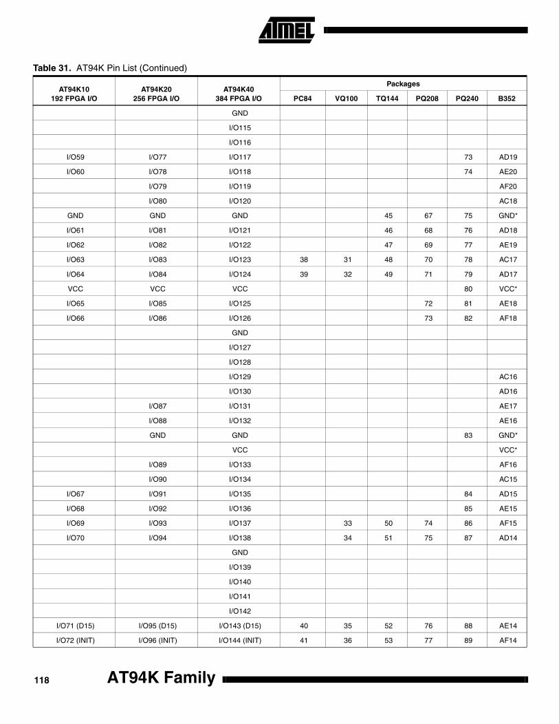
GND
I/O115
I/O116
I/O59 I/O77 I/O117 73 AD19
I/O60 I/O78 I/O118 74 AE20
I/O79 I/O119 AF20
I/O80 I/O120 AC18
GND GND GND 45 67 75 GND*
I/O61 I/O81 I/O121 46 68 76 AD18
I/O62 I/O82 I/O122 47 69 77 AE19
I/O63 I/O83 I/O123 38 31 48 70 78 AC17
I/O64 I/O84 I/O124 39 32 49 71 79 AD17
VCC VCC VCC 80 VCC*
I/O65 I/O85 I/O125 72 81 AE18
I/O66 I/O86 I/O126 73 82 AF18
GND
I/O127
I/O128
I/O129 AC16
I/O130 AD16
I/O87 I/O131 AE17
I/O88 I/O132 AE16
GND GND 83 GND*
VCC VCC*
I/O89 I/O133 AF16
I/O90 I/O134 AC15
I/O67 I/O91 I/O135 84 AD15
I/O68 I/O92 I/O136 85 AE15
I/O69 I/O93 I/O137 33 50 74 86 AF15
I/O70 I/O94 I/O138 34 51 75 87 AD14
GND
I/O139
I/O140
I/O141
I/O142
I/O71 (D15) I/O95 (D15) I/O143 (D15) 40 35 52 76 88 AE14
I/O72 (INIT) I/O96 (INIT) I/O144 (INIT) 41 36 53 77 89 AF14
Table 31. AT94K Pin List (Continued)
AT94K10192 FPGA I/O
AT94K20256 FPGA I/O
AT94K40384 FPGA I/O
Packages
PC84 VQ100 TQ144 PQ208 PQ240 B352
AT94K Family118
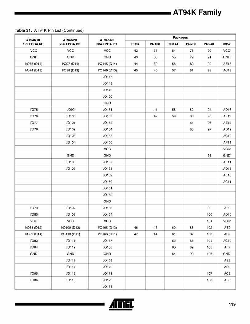
AT94K Family
VCC VCC VCC 42 37 54 78 90 VCC*
GND GND GND 43 38 55 79 91 GND*
I/O73 (D14) I/O97 (D14) I/O145 (D14) 44 39 56 80 92 AE13
I/O74 (D13) I/O98 (D13) I/O146 (D13) 45 40 57 81 93 AC13
I/O147
I/O148
I/O149
I/O150
GND
I/O75 I/O99 I/O151 41 58 82 94 AD13
I/O76 I/O100 I/O152 42 59 83 95 AF12
I/O77 I/O101 I/O153 84 96 AE12
I/O78 I/O102 I/O154 85 97 AD12
I/O103 I/O155 AC12
I/O104 I/O156 AF11
VCC VCC*
GND GND 98 GND*
I/O105 I/O157 AE11
I/O106 I/O158 AD11
I/O159 AE10
I/O160 AC11
I/O161
I/O162
GND
I/O79 I/O107 I/O163 99 AF9
I/O80 I/O108 I/O164 100 AD10
VCC VCC VCC 101 VCC*
I/O81 (D12) I/O109 (D12) I/O165 (D12) 46 43 60 86 102 AE9
I/O82 (D11) I/O110 (D11) I/O166 (D11) 47 44 61 87 103 AD9
I/O83 I/O111 I/O167 62 88 104 AC10
I/O84 I/O112 I/O168 63 89 105 AF7
GND GND GND 64 90 106 GND*
I/O113 I/O169 AE8
I/O114 I/O170 AD8
I/O85 I/O115 I/O171 107 AC9
I/O86 I/O116 I/O172 108 AF6
I/O173
Table 31. AT94K Pin List (Continued)
AT94K10192 FPGA I/O
AT94K20256 FPGA I/O
AT94K40384 FPGA I/O
Packages
PC84 VQ100 TQ144 PQ208 PQ240 B352
119

I/O174
GND
I/O175
I/O176
I/O87 I/O117 I/O177 91 109 AE7
I/O88 I/O118 I/O178 92 110 AD7
I/O89 I/O119 I/O179 93 111 AE6
I/O90 I/O120 I/O180 94 112 AE5
GND GND GND*
VCC VCC VCC*
I/O121 I/O181 AD6
I/O122 I/O182 AC7
I/O91 (D10) I/O123 (D10) I/O183 (D10) 48 45 65 95 113 AF4
I/O92 (D9) I/O124 (D9) I/O184 (D9) 49 46 66 96 114 AF3
I/O185 AE4
I/O186 AC6
GND
I/O187
I/O188
I/O93 I/O125 I/O189 67 97 115 AD5
I/O94 I/O126 I/O190 68 98 116 AE3
I/O95 (D8) I/O127 (D8) I/O191 (D8) 50 47 69 99 117 AD4
I/O96, GCK4 I/O128, GCK4 I/O192, GCK4 51 48 70 100 118 AC5
GND GND GND 52 49 71 101 119 GND*
CON 53 50 72 103 120 AD3
East Side
VCC VCC VCC 54 51 73 106 121 VCC*
RESET RESET 55 52 74 108 122 AC4
PE0 (D7) PE0 (D7) PE0 (D7) 56 53 75 109 123 AD2
PE1 PE1 PE1 57 54 76 110 124 AC3
PD0 PD0 PD0 77 111 125 AB4
PD1 PD1 PD1 78 112 126 AD1
AB3
AC2
GND
127 AA4
128 AA3
Table 31. AT94K Pin List (Continued)
AT94K10192 FPGA I/O
AT94K20256 FPGA I/O
AT94K40384 FPGA I/O
Packages
PC84 VQ100 TQ144 PQ208 PQ240 B352
AT94K Family120

AT94K Family
AB2
AC1
VCC VCC VCC*
GND GND GND*
PE2 (D6) PE2 (D6) PE2 (D6) 58 55 79 113 129 Y3
PD2 PD2 PD2 56 80 114 130 AA2
115 131 AA1
116 132 W4
GND
117 133 W3
118 134 Y2
Y1
V4
GND GND GND 81 119 135 GND*
136 V3
137 W2
PD3 PD3 PD3 82 120 138 U4
PD4 PD4 PD4 83 121 139 U3
VCC VCC VCC 140 VCC*
PE3 (D5) PE3 (D5) PE3 (D5) 59 57 84 122 141 V2
CS0 CS0 CS0 60 58 85 123 142 V1
GND
T4
T3
U2
T2
GND GND 143 GND*
VCC VCC*
T1
R4
SDA SDA SDA 124 144 R3
SCL SCL SCL 125 145 R2
GND
PD5 PD5 PD5 59 86 126 146 R1
PD6 PD6 PD6 60 87 127 147 P3
PE4 (D4) PE4 (D4) PE4 (D4) 61 61 88 128 148 P2
PE5 PE5 PE5 62 62 89 129 149 P1
Table 31. AT94K Pin List (Continued)
AT94K10192 FPGA I/O
AT94K20256 FPGA I/O
AT94K40384 FPGA I/O
Packages
PC84 VQ100 TQ144 PQ208 PQ240 B352
121
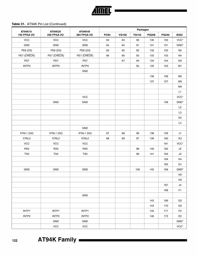
VCC VCC VCC 63 63 90 130 150 VCC*
GND GND GND 64 64 91 131 151 GND*
PE6 (D3) PE6 (D3) PE6 (D3) 65 65 92 132 152 N2
PE7 (CHECK) PE7 (CHECK) PE7 (CHECK) 66 66 93 133 153 N4
PD7 PD7 PD7 67 94 134 154 N3
INTP0 INTP0 INTP0 95 135 155 M1
GND
136 156 M2
137 157 M3
M4
L1
VCC VCC*
GND GND 158 GND*
L2
L3
K2
L4
GND
XTAL1 (D2) XTAL1 (D2) XTAL1 (D2) 67 68 96 138 159 J1
XTAL2 XTAL2 XTAL2 68 69 97 139 160 K3
VCC VCC VCC 161 VCC*
RX0 RX0 RX0 98 140 162 J2
TX0 TX0 TX0 99 141 163 J3
164 K4
165 G1
GND GND GND 100 142 166 GND*
H2
H3
167 J4
168 F1
GND
143 169 G2
144 170 G3
INTP1 INTP1 INTP1 145 171 F2
INTP2 INTP2 INTP2 146 172 E2
GND GND GND*
VCC VCC VCC*
Table 31. AT94K Pin List (Continued)
AT94K10192 FPGA I/O
AT94K20256 FPGA I/O
AT94K40384 FPGA I/O
Packages
PC84 VQ100 TQ144 PQ208 PQ240 B352
AT94K Family122

AT94K Family
TOSC1 (D1) TOSC1 (D1) TOSC1 (D1) 69 70 101 147 173 F3
TOSC2 TOSC2 TOSC2 70 71 102 148 174 G4
D1
C1
GND
D2
F4
RX1 RX1 RX1 103 149 175 E3
TX1 TX1 TX1 104 150 176 C2
D0 D0 D0 71 72 105 151 177 D3
INTP3 (CSOUT) INTP3 (CSOUT) INTP3 (CSOUT) 72 73 106 152 178 E4
CCLK CCLK CCLK 73 74 107 153 179 C3
VCC VCC VCC 74 75 108 154 180 VCC*
I/O97:144 are unbonded
I/O129:192 are unbonded
I/O193:288 are unbonded
North Side
GND GND GND 76 77 110 160 182 GND*
I/O145 (A0) I/O193 (A0) I/O289 (A0) 77 78 111 161 183 B3
I/O146, GCK7 (A1) I/O194, GCK7 (A1) I/O290, GCK7 (A1) 78 79 112 162 184 C4
I/O147 I/O195 I/O291 113 163 185 D5
I/O148 I/O196 I/O292 114 164 186 A3
I/O293
I/O294
GND
I/O295 C5
I/O296 B4
I/O149 (CS1, A2) I/O197 (CS1, A2) I/O297 (CS1, A2) 79 80 115 165 187 D6
I/O150 (A3) I/O198 (A3) I/O298 (A3) 80 81 116 166 188 C6
I/O199 I/O299 B5
I/O200 I/O300 A4
VCC VCC VCC*
GND GND GND*
I/O151 I/O201 I/O301 75 76 109 159 189 C7
I/O152 I/O202 I/O302 190 B6
I/O153 I/O203 I/O303 117 167 191 A6
I/O154 I/O204 I/O304 75* 76* 109* 168 192 D8
I/O305 C8
I/O306
Table 31. AT94K Pin List (Continued)
AT94K10192 FPGA I/O
AT94K20256 FPGA I/O
AT94K40384 FPGA I/O
Packages
PC84 VQ100 TQ144 PQ208 PQ240 B352
123
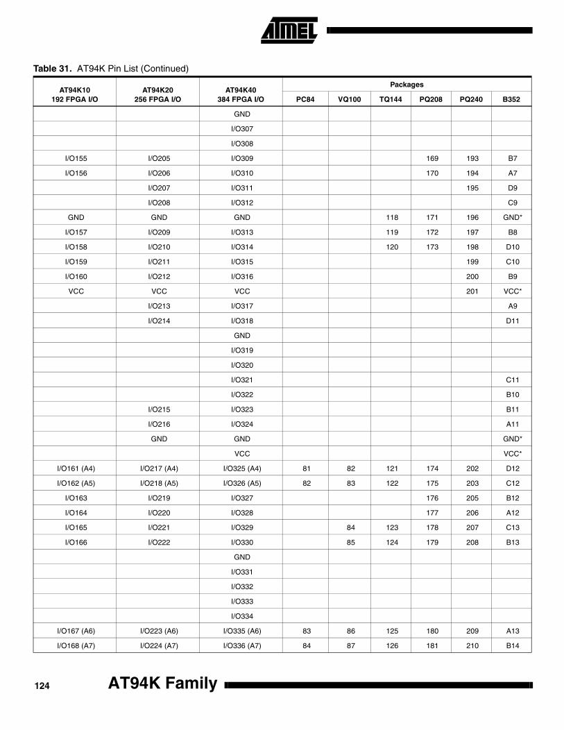
GND
I/O307
I/O308
I/O155 I/O205 I/O309 169 193 B7
I/O156 I/O206 I/O310 170 194 A7
I/O207 I/O311 195 D9
I/O208 I/O312 C9
GND GND GND 118 171 196 GND*
I/O157 I/O209 I/O313 119 172 197 B8
I/O158 I/O210 I/O314 120 173 198 D10
I/O159 I/O211 I/O315 199 C10
I/O160 I/O212 I/O316 200 B9
VCC VCC VCC 201 VCC*
I/O213 I/O317 A9
I/O214 I/O318 D11
GND
I/O319
I/O320
I/O321 C11
I/O322 B10
I/O215 I/O323 B11
I/O216 I/O324 A11
GND GND GND*
VCC VCC*
I/O161 (A4) I/O217 (A4) I/O325 (A4) 81 82 121 174 202 D12
I/O162 (A5) I/O218 (A5) I/O326 (A5) 82 83 122 175 203 C12
I/O163 I/O219 I/O327 176 205 B12
I/O164 I/O220 I/O328 177 206 A12
I/O165 I/O221 I/O329 84 123 178 207 C13
I/O166 I/O222 I/O330 85 124 179 208 B13
GND
I/O331
I/O332
I/O333
I/O334
I/O167 (A6) I/O223 (A6) I/O335 (A6) 83 86 125 180 209 A13
I/O168 (A7) I/O224 (A7) I/O336 (A7) 84 87 126 181 210 B14
Table 31. AT94K Pin List (Continued)
AT94K10192 FPGA I/O
AT94K20256 FPGA I/O
AT94K40384 FPGA I/O
Packages
PC84 VQ100 TQ144 PQ208 PQ240 B352
AT94K Family124
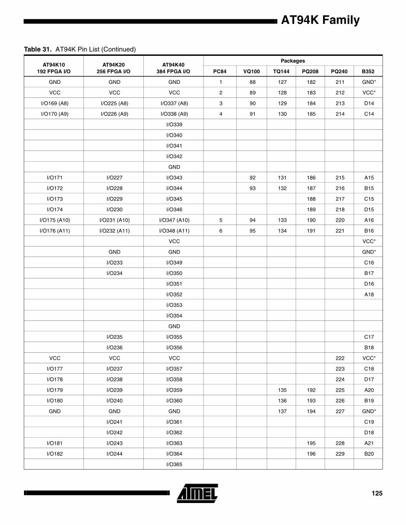
AT94K Family
GND GND GND 1 88 127 182 211 GND*
VCC VCC VCC 2 89 128 183 212 VCC*
I/O169 (A8) I/O225 (A8) I/O337 (A8) 3 90 129 184 213 D14
I/O170 (A9) I/O226 (A9) I/O338 (A9) 4 91 130 185 214 C14
I/O339
I/O340
I/O341
I/O342
GND
I/O171 I/O227 I/O343 92 131 186 215 A15
I/O172 I/O228 I/O344 93 132 187 216 B15
I/O173 I/O229 I/O345 188 217 C15
I/O174 I/O230 I/O346 189 218 D15
I/O175 (A10) I/O231 (A10) I/O347 (A10) 5 94 133 190 220 A16
I/O176 (A11) I/O232 (A11) I/O348 (A11) 6 95 134 191 221 B16
VCC VCC*
GND GND GND*
I/O233 I/O349 C16
I/O234 I/O350 B17
I/O351 D16
I/O352 A18
I/O353
I/O354
GND
I/O235 I/O355 C17
I/O236 I/O356 B18
VCC VCC VCC 222 VCC*
I/O177 I/O237 I/O357 223 C18
I/O178 I/O238 I/O358 224 D17
I/O179 I/O239 I/O359 135 192 225 A20
I/O180 I/O240 I/O360 136 193 226 B19
GND GND GND 137 194 227 GND*
I/O241 I/O361 C19
I/O242 I/O362 D18
I/O181 I/O243 I/O363 195 228 A21
I/O182 I/O244 I/O364 196 229 B20
I/O365
Table 31. AT94K Pin List (Continued)
AT94K10192 FPGA I/O
AT94K20256 FPGA I/O
AT94K40384 FPGA I/O
Packages
PC84 VQ100 TQ144 PQ208 PQ240 B352
125
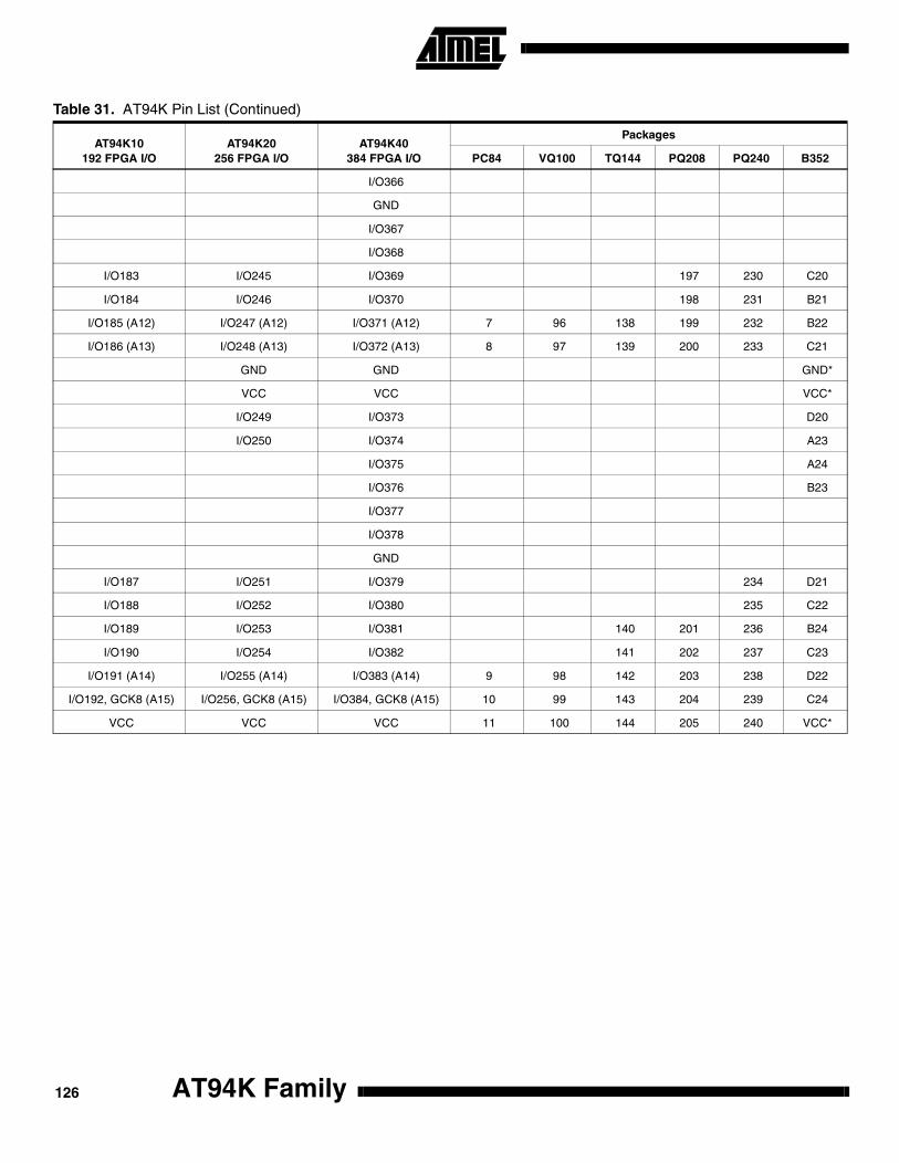
I/O366
GND
I/O367
I/O368
I/O183 I/O245 I/O369 197 230 C20
I/O184 I/O246 I/O370 198 231 B21
I/O185 (A12) I/O247 (A12) I/O371 (A12) 7 96 138 199 232 B22
I/O186 (A13) I/O248 (A13) I/O372 (A13) 8 97 139 200 233 C21
GND GND GND*
VCC VCC VCC*
I/O249 I/O373 D20
I/O250 I/O374 A23
I/O375 A24
I/O376 B23
I/O377
I/O378
GND
I/O187 I/O251 I/O379 234 D21
I/O188 I/O252 I/O380 235 C22
I/O189 I/O253 I/O381 140 201 236 B24
I/O190 I/O254 I/O382 141 202 237 C23
I/O191 (A14) I/O255 (A14) I/O383 (A14) 9 98 142 203 238 D22
I/O192, GCK8 (A15) I/O256, GCK8 (A15) I/O384, GCK8 (A15) 10 99 143 204 239 C24
VCC VCC VCC 11 100 144 205 240 VCC*
Table 31. AT94K Pin List (Continued)
AT94K10192 FPGA I/O
AT94K20256 FPGA I/O
AT94K40384 FPGA I/O
Packages
PC84 VQ100 TQ144 PQ208 PQ240 B352
AT94K Family126
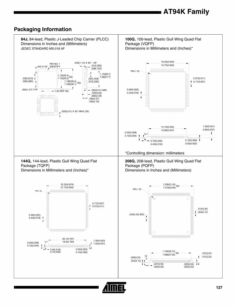
AT94K Family
Packaging Information
*Controlling dimension: millimeters
PIN 1 ID
0.56(0.022)0.44(0.018)
16.25(0.640)
15.75(0.620)
0.27(0.011)
0.17(0.007)
14.10(0.555)13.90(0.547)
0.15(0.006)0.05(0.002)
0.75(0.030)0.45(0.018)
0-70.20(0.008)0.10(0.004)
1.05(0.041)0.95(0.037)
84J, 84-lead, Plastic J-Leaded Chip Carrier (PLCC)Dimensions in Inches and (Millimeters)JEDEC STANDARD MS-018 AF
100Q, 100-lead, Plastic Gull Wing Quad Flat Package (VQFP)Dimensions in Millimeters and (Inches)*
144Q, 144-lead, Plastic Gull Wing Quad Flat Package (TQFP)Dimensions in Millimeters and (Inches)*
208Q, 208-lead, Plastic Gull Wing Quad Flat Package (PQFP)Dimensions in Inches and (Millimeters)
127
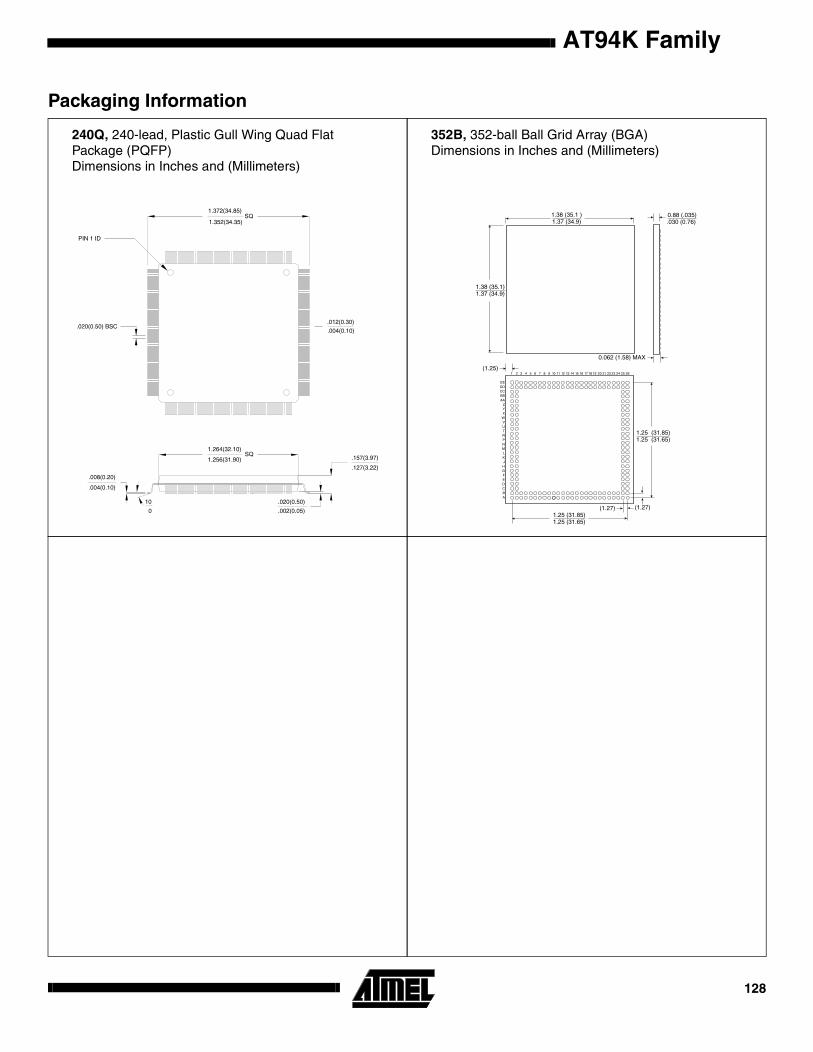
AT94K Family
Packaging Information
1.38 (35.1 )1.37 (34.9)
0.062 (1.58) MAX
EEDDCCBBAA
ZYXWVUTRPNMLKJHGFEDCBA
1(1.25)
(1.27)(1.27)
2 3 4 5 6 7 8 9 10 11 12 13 14 15 16 17
1.25 (31.85)1.25 (31.65)
1.25 (31.85)1.25 (31.65)
0.88 (.035).030 (0.76)
1819 20 21 2223 24 25 26
1.38 (35.1)1.37 (34.9)
240Q, 240-lead, Plastic Gull Wing Quad Flat Package (PQFP)Dimensions in Inches and (Millimeters)
352B, 352-ball Ball Grid Array (BGA)Dimensions in Inches and (Millimeters)
128
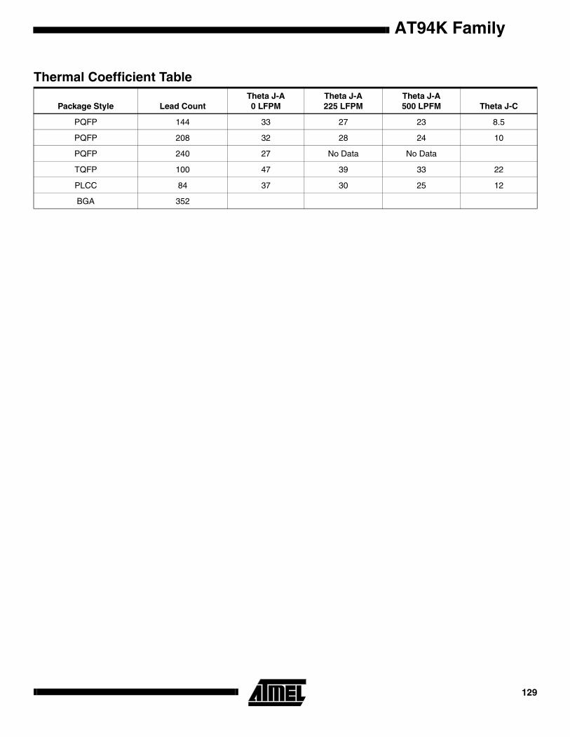
AT94K Family
129
Thermal Coefficient Table
Package Style Lead CountTheta J-A0 LFPM
Theta J-A225 LFPM
Theta J-A500 LPFM Theta J-C
PQFP 144 33 27 23 8.5
PQFP 208 32 28 24 10
PQFP 240 27 No Data No Data
TQFP 100 47 39 33 22
PLCC 84 37 30 25 12
BGA 352
© Atmel Corporation 1999.Atmel Corporation makes no warranty for the use of its products, other than those expressly contained in the Company’s standard war-ranty which is detailed in Atmel’s Terms and Conditions located on the Company’s web site. The Company assumes no responsibility forany errors which may appear in this document, reserves the right to change devices or specifications detailed herein at any time withoutnotice, and does not make any commitment to update the information contained herein. No licenses to patents or other intellectual prop-erty of Atmel are granted by the Company in connection with the sale of Atmel products, expressly or by implication. Atmel’s products arenot authorized for use as critical components in life support devices or systems.
Atmel Headquarters Atmel Operations
Corporate Headquarters2325 Orchard ParkwaySan Jose, CA 95131TEL (408) 441-0311FAX (408) 487-2600
EuropeAtmel U.K., Ltd.Coliseum Business CentreRiverside WayCamberley, Surrey GU15 3YLEnglandTEL (44) 1276-686-677FAX (44) 1276-686-697
AsiaAtmel Asia, Ltd.Room 1219Chinachem Golden Plaza77 Mody Road TsimhatsuiEast KowloonHong KongTEL (852) 2721-9778FAX (852) 2722-1369
JapanAtmel Japan K.K.9F, Tonetsu Shinkawa Bldg.1-24-8 ShinkawaChuo-ku, Tokyo 104-0033JapanTEL (81) 3-3523-3551FAX (81) 3-3523-7581
Atmel Colorado Springs1150 E. Cheyenne Mtn. Blvd.Colorado Springs, CO 80906TEL (719) 576-3300FAX (719) 540-1759
Atmel RoussetZone Industrielle13106 Rousset CedexFranceTEL (33) 4-4253-6000FAX (33) 4-4253-6001
Fax-on-DemandNorth America:1-(800) 292-8635
International:1-(408) 441-0732
Web Sitehttp://www.atmel.com
BBS1-(408) 436-4309
Printed on recycled paper.
1138B–12/99/xM
Marks bearing ® and/or ™ are registered trademarks and trademarks of Atmel Corporation.
Terms and product names in this document may be trademarks of others.


![ZYBO - Digilent Documentation [Reference.Digilentinc] Z7 B.2 out of 14 2017 MIPI, General I/O 10K R60 10K R62 10K R64 10K R67 GND VCC3V3 SW3 SW2 SW1 SW0 10K R57 10K R71 10K R72 GND](https://static.fdocuments.in/doc/165x107/5abecaa37f8b9a3a428d6851/zybo-digilent-documentation-z7-b2-out-of-14-2017-mipi-general-io-10k-r60.jpg)