109EE0602.pdf
69
EFFECT OF IMPULSE VOLTAGE ON SOLID INSULATION A Thesis submitted in partial fulfillment of the requirements for the degree of Bachelor of Technology in “Electrical Engineering” By ASHISH KUMAR SINGH(109EE0602) SULUGANTI CHANDRA PRAKASH(109EE0655) UNDER SUPERVISION PROF. SUBRATA KARMAKAR Department of Electrical Engineering NATIONAL INSTITUTE OF TECHNOLOGY Rourkela-769008,INDIA
-
Upload
rijilpoothadi -
Category
Documents
-
view
6 -
download
3
Transcript of 109EE0602.pdf
EFFECT OF IMPULSE VOLTAGE
ON SOLID INSULATION
A Thesis submitted in partial fulfillment of the requirements for the degree of
Bachelor of Technology in “Electrical Engineering”
By
ASHISH KUMAR SINGH(109EE0602)
SULUGANTI CHANDRA PRAKASH(109EE0655)
UNDER SUPERVISION
PROF. SUBRATA KARMAKAR
Department of Electrical Engineering
NATIONAL INSTITUTE OF TECHNOLOGY
Rourkela-769008,INDIA

2
DEPARTMENT OF ELECTRICAL ENGINEERING
NATIONAL INSTITUTE OF TECHNOLOGY, ROURKELA- 769 008
ODISHA, INDIA
CERTIFICATE
This is to certify that the draft report/thesis titled “Effect of impulse voltage on solid
insulation”, submitted to the National Institute of Technology, Rourkela by Mr.Ashish Kumar
Singh,Roll No: 109EE0602 and Mr.S.ChandraPrakash,Roll No. 109EE0655 for the award of
Bachelor of Technologyin Electrical Engineering, is a bonafide record of research work carried out
by him under my supervision and guidance.
The candidate has fulfilled all the prescribed requirements.
The draft report/thesis which is based on candidate’s own work, has not submitted elsewhere
for a degree/diploma.
In my opinion, the draft report/thesis is of standard required for the award of a Bachelor of
Technologyin Electrical Engineering.
Prof. S.Karmakar
Supervisor
Department of Electrical Engineering
National Institute of Technology
Rourkela – 769 008 (ODISHA)

3
Acknowledgement
The present research work related to this thesis has been carried out at the High Voltage
laboratory,Department of Electrical Engineering, National Institute of Technology,Rourkela. We
would like to acknowledge the contribution and guidance of several people without whom it
would have been impossible to carryout this work. First of all, I would like to extend my
profound gratitude to our supervisor Prof. S.Karmakar,Professor of Department of Electrical
Engineering at NIT Rourkela, for his tremendous support and consistent encouragement
throughout our research work and sharing his technical expertise which has led to many
difficulties easily. I simply thank for his exemplary guidance and encouragement in every
aspects for my career growth. His endless drive for better and new results is highly appreciated.
His trust and support inspired me in the most important moments of making right decisions and
I am glad to work under his supervision.
I am very thankful to our Head of the Department Prof. A.K. Panda for providing his timely
suggestions and with the best facilities in the Department. I extent my sincere thanks to all
faculty and non-faculty members of the Department and specially SEM lab of the Metallurgical
Department
I would like to thank my parents and friends for being with us when encountering difficulties.
Their loving support has been always most precious possession on earth
ASHISH KUMAR SINGH
S.CHANDRA PARAKASH

4
CONTENTS
Page No.
ABSTRACT 6
LIST OF FIGURES 7
LIST OF TABLES 8
LIST OF EQUATIONS 9
ACRONYMS AND ABBREVIATIONS 10
CHAPTER 1THESIS OVERVIEW
1.1 Introduction. 13
1.2 Objective. 13
1.3 Literature review. 13
1.4 Organization of the thesis. 14
CHAPTER 2 INTRODUCTION AND BREAKDOWN OF SOLID INSULATING MATERIAL
2.1 Impulse Voltage. 17
2.2 Impulse Voltage Generator. 20
2.3 Breakdown of solid insulating material. 22
2.4 Factors affecting breakdown of solid insulators. 25
2.5 Tolerances on size, shape and surface of sphere and their shanks. 29
2.6 Solid insulating material. 29
2.7 Classes of insulators. 30
CHAPTER 3 EXPERIMENTAL SETUP FOR THE EFFECT OF IMPULSE VOLTAGE ON SOLID
INSULATING MATERIAL USING SPHERE-SPHERE ELECTRODE ARRANGEMENT
3.1 Apparatus required for the effect of impulse voltage on solid insulating

5
material. 32
3.2 Description of used apparatus. 32
CHAPTER 4 EXPERIMENTAL PROCEDURE AND OBSERVATION
4.1 Sample Preparation 40
4.2 Measurement of breakdown voltage of insulating sheets 41
4.3 Monitoring of the state of solid insulating material 42
4.4 Scanning Electron Microscope (SEM) 43
4.5 Interpretation of SEM Images 44
CHAPTER 5 RESULTS AND DISCUSSION
5.1 Result 52
CHAPTER 6 CONCLUSION AND FUTURE SCOPE OF WORK
6.1 Conclusion 60
6.2 Future scope of work 61
REFERENCES

6
ABSTRACT
One of the main problems of the high voltage engineering is the degradation of the insulation
of the solid insulating material.It has been revealed through the several researches and studies
that the high voltage power equipment are directly and mainly subjected with the spark over
voltage caused by impulse voltage like lightening strokes and switching action.The sphere-
sphere electrode arrangements are mainly used for the measurement of the peak values of the
high voltages as adopted by the IEC and IEEE. Generally in the electrical power equipment, the
standard sphere gaps are widely used. The effect of the impulse voltage on different insulations
like Nomex,Lather Minilex,White Minilex and Glass Cloth has been studied.To study and
observe the effect on insulation of the solid material due to breakdown mechanism, the
insulation samples are collected after the application of the impulse voltage test and analysis is
done with the help of scanning electron microscope(SEM).A standard sphere of 25cm in
diameter is used to measure the effect of impulse voltage. Finally the experimental data is
generated and compared with the theoretical and the graphical interpretation is done.
Hence the determination of the breakdown voltage of various insulating material gives a major
area of interest to the electrical engineers and in particular to the high voltage
engineers.Therefore,the possibility of developing solid insulating materials with excellent
breakdown strength is viable through study and research.The few basic and important topics
affecting the breakdown and study of different composite insulating materials are reviewed.
7
LIST OF FIGURES
Figure No. Figure Name Page No.
2.1 Full Impulse Voltage 19
2.2 Impulse voltage generator 20
2.3 Simplified equivalent circuit of an impulse generator circuit 22
2.4 Variation of breakdown strength with time after application of voltage 23
2.5 Vertical sphere-sphere arrangement 28
3.1 Control module 33
3.2 Medium Impulse Voltage Generator 34
3.3 High Voltage Transformer 36
3.4 Sphere-Sphere Electrode 38
4.1 Scanning Electron Microscope (SEM) 44
4.2 SEM Images of Lather Minilex Paper 45
4.3 SEM Images of White Minilex Paper 47
4.4 SEM Images of Glass Cloth Paper 48
4.5 SEM Images of Nomex Paper 50
8
LIST OF TABLES
Table No. Table title Page No.
2.1 Variation of breakdown strength on application of voltage 24
2.2 Breakdown voltage of Polyethylene with thickness 27
4.1 Breakdown Voltage of Nomex Paper 42
4.2 Breakdown Voltage of Lather Minilex Paper 42
4.3 Breakdown Voltage of Glass Cloth Paper 43
4.4 Breakdown Voltage of White Minilex Paper 43

9
LIST OF EQUATIONS
S.NO EQUATION NAME PAGE NO.
1. Inverse power model 25
2. Naidu’s equation 27
3. Mason and Dakin’s equation 27

10
ACRONYMS AND ABBREVIATIONS
SEM Scanning Electron Microscope
Ɛ0 Permittivity of free space
Ɛr Relative permittivity
V Voltage
HV High voltage
VBD Breakdown voltage

11
CHAPTER 1 THESIS OVERVIEW
12
CHAPTER-1
THESIS OVERVIEW
_______________________________________
1.1Introduction
Rapid growth over recent years in the power sector of the country has given the
opportunity to the power engineers to protect the power equipment during their operating
life for reliable operation. Therefore it becomes necessary for the todays electrical
engineers to know various types of solid insulations and their properties in order to
economize the cost applications and keeping safety considerations on the other hand. One
of the main problems of the high voltage engineering is the degradation of the insulation of
the solid insulating material. It has been revealed through the several research and studies.
As the high voltage power equipment are directly and mainly subjected with the spark over
voltage caused by impulse voltage like lightening strokes and switching action. The sphere-
sphere electrode arrangements are mainly used for the measurement of the peak values of
the high voltages as adopted by the IEC and IEEE. Generally in the electrical power
equipment, the standard sphere gaps are widely used. The effect of the impulse voltage on
different insulations like Nomex,Lather Minilex,White Minilex and Glass Cloth has been
studied. To study and observe the effect on insulation of the solid material due to
breakdown mechanism, the insulation samples are collected after the application of the
impulse voltage test and analysis is done with the help of scanning electron microscope
(SEM).A standard sphere of 25cm in diameter is used to measure the effect of impulse
voltage. Finally the experimental data is generated and compared with the theoretical and
the graphical interpretation is done.

13
Thesis overview
1.2 Objective
The objective of the present thesis work is to find the effect of impulse voltage on solid
insulation material like Nomex Paper, Glass Cloth, White minilex Paper and Lather minilex
Paper. The Sphere-sphere gap geometry is used for the conduction of experiment which is
available in the high voltage laboratory of NIT Rourkela. The knowledge of the breakdown
voltage of the various solid insulating materials helps us to determine the insulation type and
their strength inorder to protect the equipment to perform efficiently and avoid failure.
1.3 Literature review
The book written on High Voltage Engineering by C.L Wadhwa has helped us to get basic
idea on the impulse voltage[1]. E.Kuffel, W.SZeangle and J.Kuffel have published book on High
Voltage Engineering Fundamentals for getting basic fundamental for our thesis work[2].Author
M.S Naidu and V. Kamaraju have published book on High Voltage Engineering which helped in
assimilating our work[3].C.Forthergill presented paper on the Ageing, space charge and
nanodielectrics[4].A short method of estimating lifetime of propylene film using steep stress
test has been conducted by P.Cygan, W. Khechen and R.Laghari[5].The residual a.c breakdown
voltage of 6.6 kV dry –cured XPLE power cable under wet – accelerated aging test has been
proposed by T.Hashizume, C.Shinoda, K.Nakamura, M.Hotta and
T.Tani[6].U.Riechert,M.Eberhardt, J.Kindersberger and J.Speek presented paper on the
breakdown behavior of polyethylene at d.c voltage stress[8].P. Basappa, S.Jang and J.Kim have
done work the electrical breakdown studies on electro active paper[9]. S. Grzybowski, E.A
Feilat, P. Knight and L. Doriott have presented paper on the breakdown voltage behavior of
thermoplastics at d.c and a.c voltages[10].The breakdown mechanism of solid insulating
material like polyethylene and nanocomposite is done by various researchers[11-13].K.

14
Elanseralathan, J. Thomas ans G.R Nagabhusana have done the work on breakdown solid
insulating materials under high frequency high voltage stress[14]. The work on determination of
aging model constants under high frequency and high electric fields has been done by W.
Khachen and J.R Laghari[15]. J.H Mason has presented the work on effect of thickness and area
on the electric strength of polymers[16].Breakdown voltage behavior of leatherite paper with
or without void is shown in paper of S.Ghosh and N.K Kishore[17].M.G Dakins has proposed
breakdown strength of silicone rubber[18].Electrical breakdown due to discharges on different
types of insulation has been proposed by C. Laurent, C. Mayoux and A.Sergeant[21]. G.L
Atkinson and W.R Thomas presented paper on an epoxy paper insulation system for high
voltage applications [24]. P.H.F Morshius has done work on the degradation of solid dielectrics
due to internal partial discharges [29]. K.S Naidu, S.K Jain, V.N Maller and P.Satyanarayan have
conducted studies on the partial discharges study non uniform fields with insulating barrier [31-
33].
1.4 ORGANIZATION OF THE THESIS
The thesis has been organized into siximportant chapters in which each chapter has its
own way of describing and analyzing the fundamentals of the work followed by theoretical and
experimental results which reveals the lubricity of the work.
Chapter 1 : The first chapter deals with basic introduction, objective of the thesis and
literature review on the Effect of Impulse Voltage on solid insulation. It also
includes the organization of the thesis.
Chapter 2 : In this chapter the basic definition of the Impulse Voltage is described and the
factors affecting the breakdown voltage of solid insulating material is studied.
The basic theoretical study of the Impulse Voltage Generator is carried out and
the breakdown mechanism in solid dielectrics is studied. It also describes the
different class of insulators.

15
Thesis overview
______________________________________________________________________________
Chapter 3 : This chapter deals with experimental setup for the breakdown voltage of solid
insulating material using standard sphere-sphere electrode arrangement. In this
chapter the apparatus required for the measurement of the effect of impulse
voltage on solid insulating material and the description of the apparatus used is
discussed.
Chapter 4 : This chapter deals with experimental procedures and observations. It covers
the task of sample preparation of the solid insulating material which is
commercially available in the market. The measurement of the breakdown
voltage of the insulating sheets, monitoring of the state of solid insulating
material and interpretation of the SEM images is done in this chapter.
Chapter 5 : This chapter deals with the results and discussion of the research work. The
graph is plotted for the characteristic performance of the insulating sheets under
various parameters such as thickness of the insulating sheet and gap geometry
of the electrodes.
Chapter 6 : Finally, in this chapter the conclusion of the project work is included and future
scope of the work for the advancement of technology is discussed.

16
CHAPTER 2 INTRODUCTION AND BREAKDOWN VOLTAGE
OF SOLID INSULATING MATERIAL

17
CHAPTER-2
INTRODUCTION AND BREAKDOWN VOLTAGE OF SOLID
INSULATING MATERIAL
____________________________________________________
2.1IMPULSE VOLTAGE
An impulse voltage is a unidirectional voltage, which, rises rapidly to a maximum value
and falls to zero instantly. The maximum value is called the peak value of the impulse voltage.
The impulse voltage is specified by this value. Small oscillations which have amplitude less than
5% of the peal value of impulse voltage are tolerated. A mean curve should be considered in
case of oscillations in the wave shape. Full impulse voltage can be defined as an impulse voltage
which develops without causing flash over or puncture.
Chopped impulse voltage can be defined as flash over or puncture occur which causes a
sudden collapse of the impulse voltage. A full impulse voltage is characterized by its peak value
and by the wave front and wave tail, which is its two time interval. The wave front time of an
impulse wave is defined as the time taken by the wave to reach to its maximum value starting
from zero value. Generally it is difficult to identify the start and peak points of the impulse wave
and so the wave front time is specified as 1.25 times (t2 – t1), where t2 is defined as the time for
the impulse wave to reach its 90% of the peak value and t1 defined as the time to reach 10% of
its peak value. Since (t2 – t1) represents 80% of the wave front time, to give total wave front
time, it is multiplied by 1.25 to give the total wave front time.. The point where the line CB
intersects the time axis is known to be the nominal starting point of the impulse wave.The
nominal wave tail time is the point on the wave tail where the voltage is 50% of the peak value
and between the nominal starting point t0 i.e. wave fail time is expressed as (t3 – t0)[1].

18
Introduction and Breakdown Voltage of Solid insulating material
______________________________________________________________________________
(a)
(b)

19
Introduction and Breakdown Voltage of Solid insulating material
______________________________________________________________________________
(c)
FIG 2.1(a)Full impulse voltage(b)Chopped on the tail impulse voltage(c)Chopped on front
impulse voltage.T1:Front time.T2:Time to half value.TC: Time to chopping.O1:Virtual origin .
2.1.1 IMPULSE FLASH OVER VOLTAGE
Whenever an impulse voltage is applied to an insulating medium of different thickness, it
is not certain that the flash over may or may not take place. If out of a total ten applications of
impulse voltage about 5 of them flash over then the probability of flash over of the impulse
voltage is 50%. However, it is to be noted that the flash over occurs at an instant subsequent to
the attainment of the peak value. The flash over also depends upon the polarity, duration of
wave front and wave tails of the applied impulse voltages. The impulse flash over

20
Introduction and Breakdown Voltage of Solid insulating material
______________________________________________________________________________
Voltage for flash over on the wave front is the value of the impulse voltage at the instant of
flash over on the wave front. If the flash over occurs more than 50% of the number of
applications, it is defined as impulse flash over voltage in excess of 50%.
The impulse puncture voltage can be defined as the peak value of the impulse voltage which
causes puncture of any material like solid insulations when puncture is on the wave tail and is
the value of the voltage at the instant when puncture occurs on the wave front. Impulse ratio
for the flash over is defined as the ratio of impulse flash over voltage to the peak value of
power frequency flash over voltage. Impulse ratio for flash over is not constant for any
particular object but depends on the polarity and the shape of the impulse voltage. The impulse
ratio for puncture is defined as the ratio of the impulse puncture voltage to the peak value of
the power frequency of the puncture voltage [1-3].
2.2IMPULSE VOLTAGE GENERATOR
FIG 2.2 Impulse voltage generator.
C2
D.C.Supply
L4
1
2
R3
R4
Test
Specimen
R2
L31 2
R1
C4
C1
L1
1
2
21
Introduction and Breakdown Voltage of Solid insulating material
______________________________________________________________________________
The figure shows the exact equivalent circuit of a single stage impulse voltage generator along
with the typical load.C1 is the capacitance of the generator which is charged a DC source to a
suitable voltage which causes discharge through the sphere gap. The capacitance C1 may
consists of a single capacitance where the generator is known as the single stage impulse
voltage generator. When C1 is the total capacitance of group of capacitors charged in parallel
and discharged in series then it is known as multi stage generator. L1 is the inductance of the
generator and leads connecting the generator to the discharge circuit and is usually kept small.
The resistance R1 consists of series resistance of the capacitances and leads to additional
lumped resistance inserted within the generator which is for damping purpose and for output
waveform control.L3 and R3 are the external elements which are connected at the generator
terminal for waveform control. The function of R2 and R4 is to control the duration of the wave.
Also R4 serves the purpose of a potential divider when a CRO is used for measurement
purposes.C2 and C4 represent the capacitances to earth of the high voltage components and
leads.C4 also contains the capacitance of the test object and of any other load capacitance
which is required for producing the required wave shape. L4 represents the inductance of the
test object and can affect the wave shape considerably. Basically for practical reasons one
terminal of the impulse voltage generator is grounded solidly. The polarity of the output
voltage is changed by changing the polarity of D.C. charging voltage [2].
For the evaluation of various impulse voltage circuit elements, its analysis using the equivalent
circuit is quite important and complex. To simplified and practical forms of impulse voltage
generator are shown in figures.

22
Introduction and Breakdown Voltage of Solid insulating material
______________________________________________________________________________
FIG 2.3 Simplified equivalent circuit of an impulse voltage generator.
The two circuits shown are widely used. They differ only in the position of the wave tail control
resistance R2.When R2 is on the load side of the R1 as shown in the figure (a) the two resistances
forms a potential divider which reduces the output voltage but when R2 is on the generator side
of R1 as shown in figure (b) this particular loss of output voltage is absent.
The impulse capacitor C1 is charged through a charging resistance to a DC voltage V0 which is
discharged by flashing over the switching gap with the suitable value of pulse. Across the load
capacitance C2 the desired impulse voltage appears. The shape of the output impulse voltage is
determined by the value of the circuit elements.
2.3 BREAKDOWN OF SOLID INSULATING MATERIAL
Solid insulation forms an important and an integral part of high voltage engineering. The
solid insulating materials insulate conductors from one another. Therefore the knowledge and
study of the failure mechanisms of solid insulating mechanisms under various electric and
voltage stresses is of great importance. However numerous investigations and research on
breakdown of solids have been done and a number of theories have been given to explain the
breakdown processes in solids still the state of knowledge in this field is very inconclusive. The
breakdown in solid insulation can be broadly categorized as [3].

23
Introduction and Breakdown Voltage of Solid insulating material
______________________________________________________________________________
(a) Intrinsic or ionic breakdown
(b) Electromechanical breakdown
(c) Failure due to treeing and tracking
(d) Thermal breakdown
(e) Electrochemical breakdown
(f) Breakdown due to internal discharges
Fig 2.4 Variation of breakdown strength with time after application of voltage.
Fothergill very clearly showed the between the breakdown and degradation of a solid insulating
material. According to him, the breakdown phenomenon that is sudden and catastrophic and
the insulation of the solid insulating material cannot withstand the service voltage which leads
to the breakdown. The degradation of solid insulating material, on the other hand takes place
over a period of time. It increases the probability of the. Breakdown process and decreases the
breakdown voltage of material. The erosion and pit formation are important in the degradation
process and are followed by tree formation and final dielectric failure. The degradation process
after a long period of hours and weeks, leads to breakdown. Well-designed insulation systems,
operated within the scope and aim of design parameters, do

24
Introduction and Breakdown Voltage of Solid insulating material
_____________________________________________________________________________
not break or degrade easily. Both these processes are irreversible. Table 2.1 shows some
of the differences between breakdown degradation for a solid insulating material [4].
Table 2.1 Shows the variation of breakdown strength on application of voltage with time.
FEATURES BREAKDOWN DEGRADATION
Effect Catastrophic insulation cannot be used
afterwards.
Leads to breakdown, reduces
breakdown voltage
Speed Fast occurs<<1s Hours and years
Evidence Direct observation by eye Observation would require
microscope
Examples Intrinsic,thermal,electromechanical,electroche
mical,partial discharge in cavities
Electrical trees, water trees
25
Introduction and Breakdown Voltage of Solid insulating material
____________________________________________________
2.4 FACTORS AFFECTING BREAKDOWN OF SOLID INSULATING
MATERIALS
The breakdown of solid insulating materials depends on the following factors:
2.4.1 NATURE OF WAVEFORM
The breakdown voltage of solid insulating materials largely depends on the nature of the
voltage waveform applied to it that is DC, AC and impulse [5-12].
2.4.2 FREQUENCY
The variation of frequency on solid insulating material has an important role to play in
affecting the breakdown voltage of solid dielectrics. At higher frequency, the breakdown
voltage is much lower than the breakdown voltage at 50 Hz [13-14].
2.4.3 AGEING
The breakdown voltage of solid insulating material decreases with the ageing of the
dielectric. The deterioration process is due to acceleration of partial discharges and heat which
is build up in the voids and micro cavities of the solid insulating materials when frequency is
increased. The constant n of the power model remains constant when frequency is increased.
The inverse power model is given by [13].
L=k*V-n (2.1)
Where L=time to failure
V=applied voltage
K and n are constants determined from the experimental data
26
Introduction and Breakdown Voltage of Solid insulating material
____________________________________________________
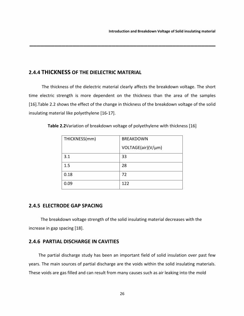
2.4.4 THICKNESS OF THE DIELECTRIC MATERIAL
The thickness of the dielectric material clearly affects the breakdown voltage. The short
time electric strength is more dependent on the thickness than the area of the samples
[16].Table 2.2 shows the effect of the change in thickness of the breakdown voltage of the solid
insulating material like polyethylene [16-17].
Table 2.2Variation of breakdown voltage of polyethylene with thickness [16]
THICKNESS(mm) BREAKDOWN
VOLTAGE(air)(V/µm)
3.1 33
1.5 28
0.18 72
0.09 122
2.4.5 ELECTRODE GAP SPACING
The breakdown voltage strength of the solid insulating material decreases with the
increase in gap spacing [18].
2.4.6 PARTIAL DISCHARGE IN CAVITIES
The partial discharge study has been an important field of solid insulation over past few
years. The main sources of partial discharge are the voids within the solid insulating materials.
These voids are gas filled and can result from many causes such as air leaking into the mold

27
Introduction and Breakdown Voltage of Solid insulating material
______________________________________________________________________________
during curing. If the voltage between the electrodes is increased to the level that the field
within the Voids goes above the breakdown strength of the gas, a partial discharge can take
place. The time taken for the breakdown to actually occur depends on the size of the cavity and
the applied voltage [19-29].
2.4.7 THICKNESS AND RELATIVE PERMITTIVITY OF THE INSULATING MATERIAL
The authors have developed mathematical relationships between the breakdown voltage
due to the partial discharge in the cavities and with the thickness and relative permittivity of
the solid insulating materials. The brief description of these relationships is as follows [30-33].
1) Naidu has shown that breakdown voltage due to the partial discharge decreases with the
increase in thickness of the material. It depends on the relative permittivity Ɛr, dielectric
strength of the air Eg, and the thickness of the material and the air gap length as
V=A*Eg (g+t/Ɛr)n (2.2)
Where A=0.9508 and n=0.3496 [31].
2)Mason and Dakin have shown that the breakdown due to the partial discharge depends on
the thickness of the material and the relative permittivity, Ɛr of the material as
V=k*(t/Ɛr)0.46 (2.3)
Where k=0.2 [32-33].

28
Introduction and Breakdown Voltage of Solid insulating material
______________________________________________________________________________
2.4.8 SPHERE GAPS
The two adjacent metal spheres of equal diameters whose separation distance is
constant form a sphere gap for the measurement of the peak value of either DC, AC or impulse
voltages.If the duration of the peak region is not too short in time, the ability to respond to the
peak values of voltages is governed by a short statistical time lag which is defined as the waiting
time for an electron to appear and to initiate an electron avalanche and breakdown streamer.
The limitation in gap distance of the sphere gaps provides a fairly homogenous field distribution
so that no corona or pre-discharge appears before breakdown. The permanent presence of
primary electrons within the regions of maximum field gradients to start avalanches within a
short time is of great importance. The electric field distribution of the sphere gaps within the
high field regions must be sufficiently controlled by the electrode geometry and the air density
[2].
Fig 2.5 1.Insulating support. 2. Sphere shank. 3. Operating gear showing maximum dimensions. 4. High
voltage connection with series resistor.5. Stress distributor. P=sparking point of high voltage sphere.
A=height of P above ground plane. B=radius of space free from external structure.

29
Introduction and Breakdown Voltage of Solid insulating material
______________________________________________________________________________
2.5 TOLERANCES ON SIZE, SHAPE AND SURFACE OF SPHERES AND
THEIR SHANKS
The spheres should be carefully made so that their surfaces are smooth and their
curvature is uniform. The diameter should not differ by 2% from the nominal value. They should
be free from surface irregularities in the region of the sparking point. The surfaces of the
spheres near by the sparking point should be free from any trace of varnish, protective coating
or grease. They should be clean and dry but not necessary to be polish. If the spheres become
excessive rough or pitted in use they should be refinished or replaced. The sphere shanks
should be reasonably in line and the shanks of the high voltage sphere should be free from
corners or sharp edges, but the diameter of the shank should not exceed 0.2D over a length D
[2].
2.6 SOLID INSULATING MATERIAL
There are various solid insulating material used in electronic and electrical equipment.
Although this list does not covers all but focuses on some of the important solid insulating
material. The various solid insulating materials can be categorized as:
CERAMIC: Ceramics are used to fabricate circuit boards, insulators and other components.The
good thermal conductivity can be complemented by the good electrical insulating properties.
EPOXY/FIBREGLASS: This type of insulating material quite good because of its superior strength
and excellent electrical properties even in humid condition.
GLASS: Glass insulation comes in a variety of forms including solid glass, fiber tapes, mats
fiberglass sheets and mats, woven tubing and cloth, and various composites. High temperature
Operation is an important feature of this type.

30
Introduction and Breakdown Voltage of Solid insulating material
______________________________________________________________________________
NOMEX: Nomex is a Dupont polyamide with working temperature range over220 degrees
centigrade and with very high voltage breakdown. It is a very good choice for Standardization
because it outperforms many other solid insulating materials.
SILICONE/FIBRE GLASS: It is a type of solid insulating material in which the glass cloth is
impregnated with a silicone resin binder that makes an excellent laminate with good dielectric
loss when it is kept dry.
PVC: Polyvinyl chloride is the most commonly used solid insulating material used. Most wiring is
insulated with PVC including house wiring. They have superior strength and excellent resistance
to heat.
2.7 CLASS OF INSULATORS
i) Class-Y insulation: Withstands a temperature of up to 90°C; typically made of
cotton, silk or paper.
ii) Class-A insulation: Withstands a temperature of up to 105°C; reinforced Class-Y
materials with impregnated varnish or insulation oil.
iii) Class-E insulation: Withstands a temperature of up to 120 degree centigrade.
iv) Class-B insulation: Withstands a temperature of up to 130°C. This has a form that
inorganic material is hardened with adhesives. This is the first insulator using this
structure.
v) Class-F insulation: Withstands a temperature of up to 155°C; for example, made of
Class-B materials that are upgraded with adhesives, silicon, and alkyd-resin varnish
of higher thermal endurance.
vi) Class H insulation: Withstands a temperature of up to 180°C; for example, made of
inorganic material glued with silicone resin or adhesives of equivalent performance.

31
CHAPTER 3
EXPERIMENTAL SETUP FOR THE EFFECT OF IMPULSE
VOLTAGE ON SOLID INSULATING MATERIAL USING
SPHERE-SPHERE ELECTRODE ARRANGEMENT

32
CHAPTER 3
EXPERIMENTAL SETUP FOR THE EFFECT OF IMPULSE VOLTAGE
ON SOLID INSULATING MATERIAL USING SPHERE-SPHERE
ELECTRODE ARRANGEMENT
____________________________________________________
3.1 APPARATUS REQIURED FOR THE EFFECT OF IMPULSE VOLTAGE ON
SOLID INSULATING MATERIAL
To conduct the effect of impulse voltage on solid insulating material using standard sphere-
sphere electrode arrangement in high voltage engineering laboratory the following apparatus is
used
(a) Haefely multitest control module type 273
(b) Impulse voltage generator
(c) Circuit breaker
(d) High voltage transformer
(e) High voltage filter
(f) Voltage divider
(g) Sphere-sphere arrangement
3.2 DESCRIPTION OF THE USED APPARATUS
The brief description of all used apparatus for impulse voltage testing on solid insulating
material is discussed below:

33
Experimental setup for the Effect of Impulse Voltage on Solid Insulating material
___________________________________________________________________________
(a) Control module
It allows comfortable and flexible control of the impulse generator system. The unit can
be connected with impulse measurement device to form an integral control and
measurement system. The unit supports manual as well as test sequence. The device is
primarily intended for use in automated test bays, which are controlled by a host computer.
Beside this the instrument can also be used for stand-alone impulse generators, which do
not require embedded solutions.
Fig 3.1Haefelymultitest set control module Type 273

34
Experimental setup for the Effect of Impulse Voltage on Solid Insulating material
___________________________________________________________________________
(b) Medium Impulse voltage generator
It is used to generate impulse voltages simulating lighting strokes and switching surges
.The state energy is 5 or 10 kJ. Maximum charging voltage is 3 MV. The basic system can be
upgraded in various ways for the special tests and for the greater ease of operation. A
number of additional circuits and components allow optimizing the impulse test system for
tests on different kind of high voltage test objects. Also the internal inductance is the
lowest.
Fig 3.2 Medium impulse voltage generator
35
Experimental setup for the Effect of Impulse Voltage on Solid Insulating material
___________________________________________________________________________
(c) Circuit breaker
The duty of circuit breakers and fuses is to rapidly interrupt fault current. When a short
circuit occurs on the power system, currents of the order of tens of thousands of Ampere
flow. A fault on the power system is usually caused by failure or breakdown of the
insulation of some equipment on the power system. Often the fault current is caused by air
breakdown due to overvoltage’s, typically caused by system disturbances by factors such as
lightning. These discharges develop into arcs, providing a path for the power frequency
follow current. The presence of these power frequency fault currents are detected by the
protection relays and the output contacts of the relays energize the circuit breaker trip
coils. The trip coils activate mechanisms that release stored energy (usually a charged
spring) to force the contacts apart to interrupt the current. This is an onerous task and the
arc quenching is assisted in various ways, depending on the type of circuit breaker. With AC
circuit breakers arc interruption is assisted by the presence of current zero crossings. The
interruption of DC arcs is more difficult.
(d) High voltage transformer
A transformer is a static device. It transfers electrical energy from one circuit to another
circuit through inductively coupled conductors the transformer's coils. A varying current in
primary winding creates a varying magnetic flux in the transformer's core and thus a varying
magnetic field through the secondary winding. This varying magnetic field induces a varying
electromotive force (EMF) in the secondary winding. This effect is called mutual induction.
In this arrangement high voltage step up transformer having power rating of 15 kVA,
400V/100kV is used which is shown in Fig. 3.2. As the voltage goes up, the current goes
down by the same proportion.

36
Experimental setup for the Effect of Impulse Voltage on Solid Insulating material
___________________________________________________________________________
Figure 3.3High Voltage Transformer
(e) Voltage divider
Voltage divider is fast and has good response parameters. Therefore they are normally
used for the measurements of full and front chopped lighting impulses or impulse voltage
with steep wave fronts. The response time of the divider is in accordance with IEC 600060.
37
Experimental setup for the Effect of Impulse Voltage on Solid Insulating material
___________________________________________________________________________
Resistive voltage dividers are used when an additional capacitance in the test circuit is not
permissible due to the slowdown effect of the time rise. The voltage divider cannot be used
as a load .This voltage divider cannot be used as a load capacitor for the impulse generator.
(f) High voltage filter
In high voltage power networks are suffered mainly with higher order harmonics
in the supply, to reduce these harmonics high voltage filters are mostly used. Due to
the higher order harmonics; increased losses, resonance problems between the inductive
and capacitive parts of the power network, overloading of capacitors, leading to
malfunctioning and premature aging, interference with telecommunications and
computers, disturbances in ripple control systems and high currents in neutral conductors
problems are occurred. These filters have several benefits like higher power factor,
improved voltage stability and network losses, filtering of harmonics in the system,
avoidance of resonance problems and amplification of electrical disturbances
.
(g) Sphere - Sphere electrode
Two electrode of spherical in shape which are identical are used for the measurement of
the breakdown voltage of insulating sheet. The sphere electrodes are made of aluminum
coated with nickel and air acts as the insulating medium. The sphere electrodes used for the
experiment is vertically aligned. The top sphere electrode is connected to the HV connector
whereas the down electrode is grounded. The used sphere electrode has the diameter of 25
cm each. Before conducting the experiment the two electrodes are cleaned so that the dust

38
Experimental setup for the Effect of Impulse Voltage on Solid Insulating material
___________________________________________________________________________
Particles residing over the surface are cleaned. As the surface of the electrode is non-
uniform, anon-uniform electric field is generated as we apply the high voltage between the
sphere electrodes. A 50 Hz transformer with a power rating of 15 kVA and transformation
ratio of 400V/100kV, the HV electrode is energized.
Fig 3.4Sphere-Sphere Arrangement

39
CHAPTER 4 EXPERIMENTAL PROCEDURE AND
OBSERVATIONS

40
CHAPTER-4
EXPERIMENTAL PROCEDURE AND OBSERVATIONS
____________________________________________________
As mentioned earlier the primary object of the present thesis work is to see the state of the
various solid insulating materials under the effect of impulse voltage and its suitability for
different application in power system application .In order to carry out above objective
scanning electron microscope (SEM) is used. Breakdown voltage of various solid insulating
materials is generated experimentally under the effect of impulse voltage. In addition the
experimental data is graphically analyzed.
4.1 SAMPLE PREPARATION
In order to find the effect of impulse voltage on solid insulating material, four commercially
available insulating sheets namely nomex, lather minilex, glass cloth and white minilex paper of
different thickness are used. The variation of thickness of these insulating are as follows:
Nomex : 5 mm and 7mm (Grey in color)
Glass cloth: 5mm and 7 mm (Yellow in color)
Lather minilex: 5mm and 7mm (Brown in color)
White minilex: 5mm and 7mm (White in color)
Before testing the effect of impulse voltage on solid insulating sheets, the procedure was
followed as laid down in ASTM handbook. This makes sure that the surface insulating sheet is
clean and dry, since contamination of the insulating sheet with dust particles and moisture may
affect the result.
41
Experimental procedure and observation
____________________________________________________
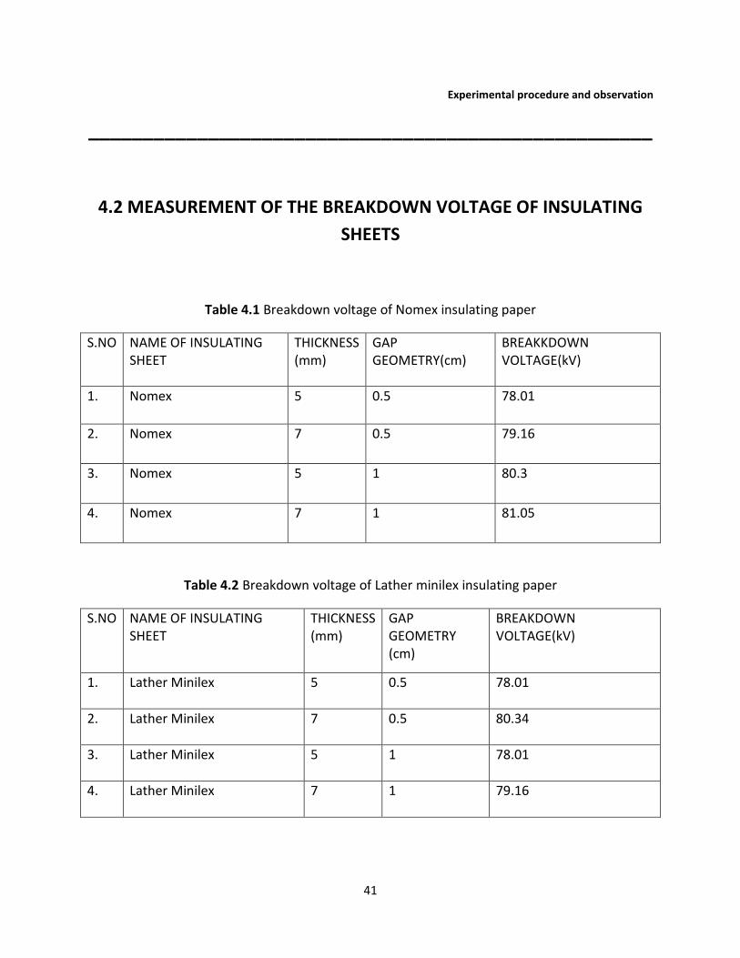
4.2 MEASUREMENT OF THE BREAKDOWN VOLTAGE OF INSULATING
SHEETS
Table 4.1 Breakdown voltage of Nomex insulating paper
S.NO NAME OF INSULATING SHEET
THICKNESS (mm)
GAP GEOMETRY(cm)
BREAKKDOWN VOLTAGE(kV)
1. Nomex 5 0.5 78.01
2. Nomex 7 0.5 79.16
3. Nomex 5 1 80.3
4. Nomex 7 1 81.05
Table 4.2 Breakdown voltage of Lather minilex insulating paper
S.NO NAME OF INSULATING SHEET
THICKNESS (mm)
GAP GEOMETRY (cm)
BREAKDOWN VOLTAGE(kV)
1. Lather Minilex 5 0.5 78.01
2. Lather Minilex 7 0.5 80.34
3. Lather Minilex 5 1 78.01
4. Lather Minilex 7 1 79.16

42
Experimental procedure and observation
____________________________________________________
Table 4.3 Breakdown voltage of Glass cloth insulating paper
S.NO NAME OF INSULATING SHEET
THICKNESS(mm) GAP GEOMETRY (cm)
BREAKDOWN VOLTAGE
1. Glass Cloth 5 0.5 76.85
2. Glass Cloth 7 0.5 80.34
3. Glass Cloth 5 1 76.85
4. Glass Cloth 7 1 78.01
Table 4.4 Breakdown voltage of White minilex insulating paper
S.NO NAME OF INSULATING SHEET
THICKNESS (mm)
GAP GEOMETRY (cm)
BREAKDOWN VOLTAGE(kV)
1. White Minilex 5 0.5 72.19
2. White Minilex 7 0.5 73.35
3. White minilex 5 1 80.3
4. White minilex 7 1 81.5
4.3 MONITORING OF THE STATE OF SOLID INSULATING MATERIALS
Apart from the generation of the breakdown voltage of the insulating sheets
experimentally, the monitoring of the state of the insulating sheet is very important and
43
Experimental procedure and observation
____________________________________________________
challenging task. In order to monitor the state of the insulating sheet at various voltage
stresses, scanning electron microscope (SEM) is utilized. The SEM was operated under low
vacuum mode, in order to visualize and observe the sample, which otherwise would be difficult
due excessive surface charging.
4.4 SCANNING ELECTRON MICROSCOPE (SEM)
A scanning electron microscope (SEM) is a type of electron microscope that uses high
energy beam of electrons in a raster scan pattern to find the image of the sample by scanning
it. The electrons interact with the atoms that make up sample producing signals and that
contain information about the samples composition, surface topography, and other properties
such as electrical conductivity. Secondary electrons back scattered electrons (BSC),
characteristic X-rays, Specimen current, transmitted electrons and light (cathodoluminescence)
are some of the types of signals produced by an scanning electron microscope. It is rare that a
single machine would have detector for all possible signals but secondary electron detectors
are common in all scanning electron microscopes. The signals result from the interaction of the
atoms at or near the surface of the samples with electron beams. In most common or standard
detection mode, the SEM can produce very high resolution images of a sample surface
revealing information and details about less than 1 to 5 nm in size. This is known as secondary
electron imaging or SEI. SEM micrographs have a large depth of field yielding due to very
narrow electron beam; a characteristic three dimensional appearance can be obtained which
could be useful for understanding the surface structure of the sample.
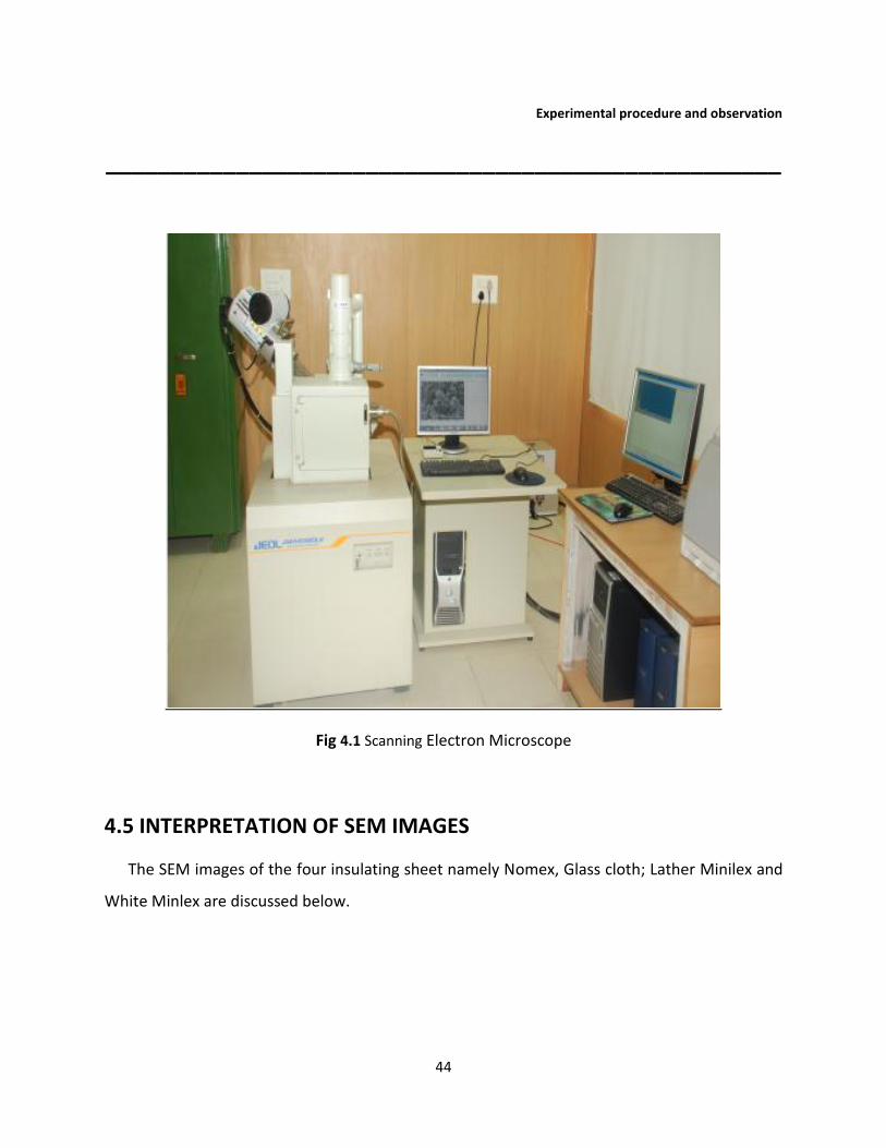
The SEM test is conducted at SEM laboratory in the Metallurgical Department, NIT Rourkela
using JEOL-JSM-6408LV SEM instrument. The figures of the four insulating sheet namely nomex,
lather minilex, white minilex and glass cloth after the effect of impulse voltage was taken by
SEM.
44
Experimental procedure and observation
____________________________________________________
Fig 4.1 Scanning Electron Microscope
4.5 INTERPRETATION OF SEM IMAGES
The SEM images of the four insulating sheet namely Nomex, Glass cloth; Lather Minilex and
White Minlex are discussed below.

45
Experimental procedure and observation
(a)
(b)
Fig 4.2SEM observation Of Lather Minilex Paper (a) Virgin sample(b) Stressed sample

46
Experimental procedure and observation
____________________________________________________
Figure 4.2 shows the SEM observations for the (a) virgin samples of Lather Minilex paper. The
breakdown of the sample took place at a voltage level of 78.01kV. The accelerated voltage of
the scanning electron microscope was kept at 15kV and the vacuum level was 30Pa. The center
of the lather minilex paper was magnified to 200 times. Figure (a) clearly shows the healthy
sample of the lather minilex paper. Figure (b) shows the increased roughness of the sample
with shallow cracks and some spots.
Figure 4.3 shows the SEM observations for the (a) virgin samples of White minilex
paper. The breakdown of the sample took place at a voltage level of 80.34kV. The accelerated
voltage of the scanning electron microscope was kept at 15kV and the vacuum level was 30Pa.
The center of the White Minilex paper was magnified to 200 times. Figure (a) clearly shows the
healthy sample of the White Minilex paper. Figure (b) shows the increased roughness of the
sample with shallow cracks and some spots.

47
Experimental procedure and observation
____________________________________________________
(a)
(b)
Fig4.3SEM observation Of White Minilex Paper (a) Virgin sample (b) stressed sample

48
Experimental procedure and observation
(a)
(b)
Fig4.4SEM observation Of Glass Cloth (a) Virgin sample (b) Stressed sample

49
Experimental procedure and observation
____________________________________________________
Figure 4.4 shows the SEM observations for the (a) virgin samples of Glass Cloth paper. The
breakdown of the sample took place at a voltage level of 78.01kV. The accelerated voltage of
the scanning electron microscope was kept at 15kV and the vacuum level was 30Pa. The centre
of the Glass Cloth paper was magnified to 250 times. Figure (a) clearly shows the healthy
sample of the glass cloth paper. Figure (b) shows the increased roughness of the sample with
shallow cracks and some spots.
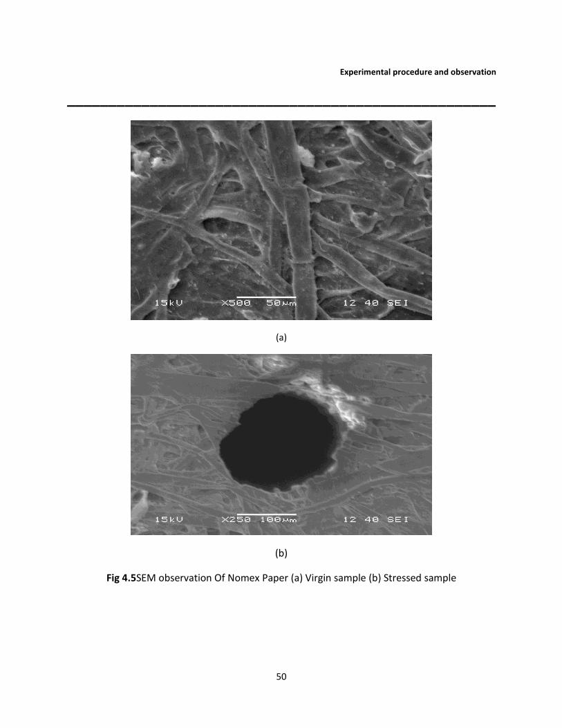
Figure4.5 shows the SEM observations for the (a) virgin samples of Nomex paper. The
breakdown of the sample took place at a voltage level of 80.34kV. The accelerated voltage of
the scanning electron microscope was kept at 15kV and the vacuum level was 30Pa. The center
of the Nomex paper was magnified to 250 times. Figure (a) clearly shows the healthy sample of
the Nomex paper. Figure (b) shows the increased roughness of the sample with shallow cracks
and some spots.
50
Experimental procedure and observation
____________________________________________________
(a)
(b)
Fig 4.5SEM observation Of Nomex Paper (a) Virgin sample (b) Stressed sample

51
CHAPTER 5 RESULTS AND DISCUSSIONS
52
CHAPTER 5
RESULTS AND DISCUSSIONS
____________________________________________________
The effect of impulse voltage on various solid insulating materials like Nomex paper,
Lather Minilex, Glass Cloth and White Minilex sheets was experimentally performed in the
sphere - sphere electrode arrangement and experimental data was obtained. The graph was
plotted for the breakdown voltage of insulating sheets against the thickness of the insulating
sheet. On analyzing the graph 5.1(a) it was obtained that breakdown voltage for the various
insulating sheet increases as the thickness of the material was increased. The graph is plotted
for the gap distance of 0.5 c.m. The graph 5.1(b) was plotted for the same parameters and was
inferred that Lather Minilex is better insulating material compared to the Nomex paper as the
slope of the Lather Minilex was more than the Nomex paper slope. The graph 5.1(c) was plotted
for the Glass cloth and White Minilex paper for the same parameter and was inferred that Glass
cloth is better than White Minilex for insulating purpose at high voltage. The graph 5.1(d) was
plotted for the parameter of breakdown voltage and gap geometry of the electrode. The
thickness of the material was 5 mm for all material. On analysis of the graph 5.1(d) it was
inferred that breakdown voltage of the insulating sheet increases as the gap distance is
increased. The graph 5.1(e) was plotted for the same parameter for Nomex, Lather Minilex and
Glass Cloth. The graph 5.1(f) was plotted for same parameter for lather minilex, glass cloth and
white minilex .The graph 5.1(g) was plotted for same parameter but the thickness of all the
material was kept 7mm.

53
Results and Discussions
____________________________________________________
FIG 5.1(a).Variation of Breakdown Voltage with Thickness of insulating sheets.
Graph 5.1(a) shows the curve variation for the breakdown voltage with the thickness of the
material for all insulating sheets namely Glass Cloth, Nomex, White Minilex and Lather Minilex
paper. From the graph it is clear that as the thickness of the glass cloth increases there is a
considerable increase in its breakdown voltage. Nomex insulating sheet has the breakdown
voltage lower than the Glass Cloth and Lather Minilex while White Minilex has the lowest
breakdown voltage among the all insulating sheets.

54
Results and Discussions
____________________________________________________
FIG 5.1(b).Variation of Breakdown voltage with thickness of insulating sheet for Nomex and
Lather Minilex.
Graph 5.1(b) shows the comparison of the breakdown voltage with thickness of the insulating
sheet for Nomex and Lather Minilex.The curve variation clearly shows that Lather Minilex is
better insulating material at high voltage than the Nomex insulating sheet.
77
78
79
80
81
82
83
4 5 6 7 8 9 10
BR
EAK
DO
WN
VO
LTA
GE
(kV
)
THICKNESS OF INSULATING SHEET(mm)
NOMEX
LATHER MINILEX

55
Results and Discussions
____________________________________________________
FIG 5.1(c)Variation of Breakdown Voltage with thickness of insulating sheet for Glass Cloth and
White Minilex.
Graph 5.1(c) shows the comparison of the breakdown voltage with thickness of the
insulating sheet for Glass Cloth and White Minilex.The curve variation clearly shows that Glass
Cloth is better insulating material at high voltage than the White Minilex insulating sheet as the
slope of Glass Cloth is more than the White Minilex.
71
73
75
77
79
81
83
4 5 6 7 8 9 10
BR
EAK
DLO
WN
VO
LTA
GE
(kV
)
THICKNESS OF INSULATING SHEET(mm)
GLASS CLOTH
WHITE MINILEX

56
Results and Discussions
____________________________________________________
FIG 5.1(d) Variation of Breakdown Voltage with Gap Geometry of Sphere-Sphere Electrode for
Nomex, Lather Minilex, Glass Cloth and White Minilex.(5 mm thickness).
The graph 5.1(d) shows the variation for the breakdown voltage of the insulating sheet with
gap geometry of the electrode sphere. From the graph it is clear that as the gap distance of the
sphere electrode increases the breakdown voltage of the solid insulating material increases.The
graph shows the variation of breakdown voltage of solid insulating material with gap geometry
for all the insulating sheets keeping thickness 5 mm.
71
73
75
77
79
81
83
85
87
89
0.4 0.9 1.4
BR
EAK
DO
WN
VO
LTA
GE(
kV)
SPHERE GAP (cm.)
NOMEX
LATHER MINILEX
GLASS CLOTH
WHITE MINILEX

57
Results and discussions
FIG 5.1 (e) Variation of Breakdown Voltage with Gap Geometry of Sphere-Sphere Electrode for
Nomex, Lather Minilex and Glass Cloth.
The graph shows the variation of the breakdown voltage of the solid insulating sheet with
gap geometry of the electrode for Nomex, Lather Minilex and glass cloth. The graph clearly
shows that Nomex has better insulating property than Lather Minilex and glass cloth when the
thickness of entire insulating sheet was kept 5 mm.
75
76
77
78
79
80
81
82
83
84
0.4 0.6 0.8 1 1.2 1.4 1.6BR
EAK
DO
WN
VO
LTA
GE
(kV
)
SPHERE GAP (cm.)
NOMEX
LATHER MINILEX
GLASS CLOTH

58
Results and Discussions
______________________________________________________________________________
FIG 5.1(f).Variation of Breakdown Voltage with Gap Geometry of Sphere-Sphere Electrode for
Lather Minilex, Glass Cloth and White Minilex.
The graph shows the variation of the breakdown voltage of the solid insulating sheet with
gap geometry of the electrode for White Minilex, Lather Minilex and Glass Cloth. The graph
clearly shows that Lather Minilex has better insulating property as its slope is greater than
white minilex and glass cloth when the entire thickness of the insulating sheet was kept 5 mm.
71
73
75
77
79
81
83
85
87
89
0.4 0.6 0.8 1 1.2 1.4 1.6
BR
EAK
DO
WN
VO
LTA
GE
(kV
)
SPHERE GAP (cm.)
LATHER MINILEX
GLASS CLOTH
WHITE MINILEX

59
Results and discussions
FIG 5.1(g).Variation of Breakdown Voltage with Gap Geometry of Sphere-Sphere Elecrode for
Nomex,Lather Minilex, Glass Cloth and White Minilex(7 mm thickness).
Graph 5.1 (g) shows the curve variation for the breakdown voltage with gap geometry of the
sphere- sphere electrode arrangement for Nomex, Glass Cloth, White Minilex and Lather
Minilex when thickness of the entire insulating sheet was kept 7mm.
73
75
77
79
81
83
85
87
89
0 0.5 1 1.5 2
BR
EAK
DO
WN
VO
LTA
GE
(kV
)
SPHERE GAP ( cm. )
NOMEX
LATHER MINILEX
GLASS CLOTH
WHITE MINILEX

60
CHAPTER 6 CONCLUSIONS AND FUTURE SCOPE OF WORK
61
CHAPTER-6
CONCLUSIONS AND FUTURE SCOPE OF WORK
____________________________________________________
6.1 CONCLUSION
It becomes necessary for the todays electrical engineers to know various types of solid
insulations and their properties in order to economize the cost applications and keeping safety
considerations on the other hand. One of the main problems of the high voltage engineering is
the degradation of the insulation of the solid insulating material. It has been revealed through
the several research and studies. As the high voltage power equipment are directly and mainly
subjected with the spark over voltage caused by impulse voltage like lightening strokes and
switching action. The sphere-sphere electrode arrangement is mainly used for the
measurement of the peak values of the high voltages as adopted by the IEC and IEEE. Generally
in the electrical power equipment, the standard sphere gaps are widely used. The effect of the
impulse voltage on different insulations like Nomex,Lather Minilex,White Minilex and Glass
cloth has been studied. To study and observe the effect on insulation of the solid material due
to breakdown mechanism, the insulation samples are collected after the application of the
impulse voltage test and analysis is done with the help of scanning electron microscope (SEM).A
standard sphere of 25cm in diameter is used to measure the effect of impulse voltage. Finally
the experimental data is generated and compared with the theoretical and the graphical
interpretation is done. Hence the determination of the breakdown voltage of various insulating
material gives a major area of interest to the electrical engineers and in particular to the high
voltage engineers. Therefore, the possibility of developing solid insulating materials with
excellent breakdown strength is viable through study and research.
62
Conclusions and Future Scope of Work
____________________________________________________
6.2 FUTURE SCOPE OF THE WORK
The present research work is focused on the experimental validation of the breakdown
characteristics in high voltage test laboratory of the solid insulating material like Lather Minilex,
Glass Cloth, White Minilex and Nomex paper and comparison is made with the theoretical
calculations. The complete analysis provides an analytical framework for designing the
withstand capacity of the high voltage insulation systems. This study can be extended for
analyzing breakdown and pre-breakdown strength of the solid insulating material and the
performance characteristics for measuring AC, DC and impulse voltages. This work also gives
the future work opportunity using different types of electrodes (i.e., needle-plate, plate-plate,
needle-sphere, rod-rod etc.).
63
REFERENCES

64
REFERENCES
______________________________________________________________________________
[1] C. L. Wadhwa, “High Voltage Engineering”, published by New Age International (P)
Limited,2nd edition 2007.
[2] E.Kuffel, W.S. Zeangle& J. Kuffel, “High Voltage Engineering Fundamentals”, published
by Butterworth-Heinemann 2nd edition, 2000.
[3] M.S. Naidu and V. Kamaraju, “High Voltage Engineering”, published by Tata McGraw-Hill
3rd edition, 2004.
[4] C. Fothergill, “Ageing, Space Charge and Nanodielectrics: Ten things we don’t know
about dielectrics”,IEEE 9thInternational Conference on Solid Dielectrics, U.K.,
Winchester, July 2007,pp. 1-10.
[5] J. R. Laghari, P. Cyganand W. Khechen, “A Short method of estimating lifetime
of Polypropylene film using step-stress Tests”, IEEE Transactions on Electrical Insulation,
Vol. 25.
[6] T. Hashizume, C.Shinoda, K.Nakamura, M.Hotta and T. Tani, “The residual ac Breakdown
voltage of 6.6 kV Dry – Cured XLPE Power Cable under wet-accelerated aging tests”, IEEE
Transactions on Dielectrics and Electrical Insulation, Vol. 5, No.2, April 98, pp. 169-173.
[7] U. Riechert, M. Eberhardt, J. Kindersberger and J. Speek, “Breakdownbehaviour of
Polyethylene at dc voltage Stress”, IEEE International Conference on Conduction and
Breakdown in Solid Dielectrics, 2008, pp. 510-513.
[8] P. Basappa, S. Jang and J. Kim, “Electrical Breakdown Studies on Electro-Active Paper”,
IEEE Transactions on Dielectrics and Electrical Insulation, Vol. 14, No. 5, Oct. 2007, pp.
1125-1132.
[9] S. Grzybowski, E. A. Feilat, P. Knight and L. Doriott, “Breakdown voltage behaviour of
PET thermoplastics at dc and ac voltages”, Proceedings of IEEE, Southeastcon, U.S.A.,
Kentucky, 1999, pp. 284-287.
Nedjarand A. Beroual, “Aging under ac voltage of Polyurethane by Weibull “IEEE.
[10] Y. Yin, X. Dong, Z. Li and X. Li, “The effect of electrically prestressing on dc
breakdown strength in the nanocomposite of low density Polyethylene/ Nano SiOx”,
IEEE, 9th International Conference on Solid Dielectrics, U.K., Winchester, July 2007, pp.
372-376.
[11] T. Mori, T. Matsaoka and T. Mizutani, “The breakdown mechanism of Poly-p-
xylene film”, IEEE Transactions on Dielectrics and Electrical Insulation, Vol. No. 1, Feb.
1994, pp. 71-76.

65
K. Elanseralathan, J. Thomas and G.R. Nagabhusana, “Breakdown of solid insulating
materials under high frequency high voltage Stress”, Proceedings of the 6th
International Conference on Properties and Applications Of Dielectric Materials, China,
June 2000, pp. 999-1001.
[12] W. Khachen and J. R. Laghari, “Determination of aging-model constants under
high frequency and high electric fields”, IEEE Transactions on Dielectrics and Electrical
Insulation, Vol. 1, No. 6, Dec. 1994, pp. 1034-1038.
[13] J. H. Mason, “Effect of thickness and area on the electric strength of polymers”,
IEEE Transactions on Electrical Insulation, Vol. 26, No. 2, April 1991, pp. 318-322.
[14] S. Ghosh and N. K. Kishore, “Breakdown voltage behaviour of Leatherite paper
with or without a void,” Proceedings of IEEE Conference, ICIT, India, Mumbai, 2006, pp.
2990-2992.
[15] M.G. Danikas, “On the breakdown strength of Silicon Rubber”, IEEE Transactions
on Dielectrics and Electrical Insulation, Vol. 1, No. 6, Dec. 1994, pp. 1196-1200.
[16] C.A. Bailey, “A study of internal discharges in cable insulation”, IEEE Transactions
on Electrical Insulation,Vol. EI-2, No. 3, 1967, pp.155-159.
[17] F. J. Pohnan, “Voids and wax in solid high-voltage cables”, AIEE Transactions on
Electrical Insulation, Vol. 70, Issue 2, 1951, pp. 1372-1376.
[18] C. Laurent, C. Mayoux and A. Sergent, “Electrical breakdown due to discharges in
different types of insulation”, IEEE Transactions on Electrical Insulation ,Vol. EI-16, No. 1,
1981, pp.52-58.
[19] A.W.W. Cameron, “Diagnoses of ac generator insulation condition by
nondestructive tests”, Power Apparatus and Systems, Part III, Transactions of A.I.E.E.,
Vol. 71, 1952, pp. 263-274.
[20] G.J. Crowdes, “A 35 kV Polyethylene-insulated cable insulation”, Power
Apparatus and Systems, Part III, Transactions of A.I.E.E., Vol. 78, 1959, pp. 1086-1090.
[21] G.L. Atkinson and W.R. Thomas, “An Epoxy-paper insulation system for high-
voltage applications”, IEEE Transactions on Electrical Insulation, Vol. EI-2, No. 1, 1967,
pp. 1824.
[22] D.A. Nattrass, “Partial discharge XVIII: The early history of partial discharge
research”, IEEE Electrical Insulation Magazine , Vol. 9, No. 4, 1993,pp. 27-31.
[23] F.H. Kreuger, M.G. Wezelenburg, A.G. Wiemer and W.A. Sonneveld, “Partial
discharge part XVIII: errors in the location of partial discharges in high voltage cables”,
IEEE Electrical Insulation Magazine, Vol. 9, No. 6, 1993, pp. 15-25.
[24] T. Tanaka, Y. Ohki, M. Ochi , M. Harada and T. Imai, “Enhanced partial discharge
resistance of Epoxy/ Clay nanocomposite prepared by newly developed organic
modification and solubilization methods” ,IEEE Transactions on Dielectrics and
66
Electrical Insulation ,Vol. 15, No. 1, 2008, pp. 81-89.
[25] Y. Kikuchi, T. Murata, Y.Uozumi, N. Fukumoto, M. Nagata, “Effects of ambient
humidity and temperature on partial discharge characteristics of conventional and
nanocompsite enameled magnet wires” ,IEEE Transactions on Dielectrics and Electrical
Insulation , Vol. 15,No. 6, 2008, pp. 1617-1625.
[26] P. H.F. Morshuis, “Degradation of solid dielectrics due to internal partial
discharge: some thoughts on progress made and where to go now”, IEEE Transactions
on Dielectrics and Electrical Insulation , Vol.12, No. 5, 2005, pp. 905-913.
[27] S. Cygan and J.R. Laghari, “Dependence of the electric strength on the thickness,
area and volume of polypropylene”, IEEE Transactions on Electrical Insulation , Vol.22,
No. 6, 1987, pp. 835-837.
[28] K.S. Naidu, S.K. Jain, V.N. Maller and P. Satyanarayana, “Partial discharge studies
in non-uniform fields with insulating barriers”, IEEE Transaction on Electrical Insulation
,Vol. EI-14, No. 5, 1979, pp. 285-287.
[29] J.H. Mason, “Discharges”, IEEE Transactions on Electrical Insulation ,Vol. EI-13,
No.4, 1978, pp. 211-238.
[30] T.W. Dakin, H.M. Philofsky and W.C. Divens ,“Effect of electric discharges on
breakdown of solid insulation”, Transactions A.I.E.E. Electrical Insulation ,73, pt.1, 1954,
pp. 155-162.

67
.

68

69