1 java applet-based virtual laboratory for emi/emc training
54
1 JAVA APPLET-BASED VIRTUAL LABORATORY FOR EMI/EMC TRAINING C. Christopoulos*, A.C. Cangellaris**, U. Ravaioli** and J. Schutt-Ainé** (*) School of Electrical and Electronic Engineering, University of Nottingham,NG7 2RD, UK Ph:+44 115 951 5580; Fax:+44 115 951 5616 [email protected] (**) ECE Department, University of Illinois at Urbana-Champaign 1406 W. Green Street, Urbana, IL 61801, USA Ph: 217-333-6037; Fax: 217-333-5962; [email protected], [email protected], [email protected] The objectives of this Tutorial are to explain some of the basic EMI/EMC interactions through the application of numerical experimentation based on the use of applets. The advantages of this approach are twofold: First, complex mathematics are avoided thus focusing on physical principles and making this material accessible to a wider audience. Second, sophisticated computer codes and numerical techniques are not employed giving the user an easy to drive interface which resembles the simplicity and immediacy of a physical experiment. The emphasis of the Tutorial is on fundamentals and no attempt is made to tackle complex problems. The Tutorial is based around a Powerpoint presentation describing the strengths and limitations of the models employed. These models are then implemented as Java Applets and are embedded in the presentation. Thus, an interactive simulation environment is provided that enables engineers to explore how each parameter affects EMC and thus help them to devise effective approaches to mitigation. The Tutorial focuses on three fundamental aspects of EMI/EMC namely electromagnetic shielding, electromagnetic emissions, and electromagnetic immunity. Internet access to selected Java Applets for personal use after completion of the Tutorial will be given to all registered Tutorial participants. Keywords: Electromagnetic Compatibility, EMC/EMI Training, Electromagnetic Shielding, Emission, Immunity.
Transcript of 1 java applet-based virtual laboratory for emi/emc training
1
JAVA APPLET-BASED VIRTUAL LABORATORY FOR EMI/EMC TRAINING
C. Christopoulos*, A.C. Cangellaris**, U. Ravaioli** and J. Schutt-Ainé**
(*) School of Electrical and Electronic Engineering, University of Nottingham,NG7 2RD, UKPh:+44 115 951 5580; Fax:+44 115 951 5616
[email protected] (**) ECE Department, University of Illinois at Urbana-Champaign
1406 W. Green Street, Urbana, IL 61801, USAPh: 217-333-6037; Fax: 217-333-5962;
[email protected], [email protected], [email protected]
The objectives of this Tutorial are to explain some of the basic EMI/EMC interactions through the application of numerical experimentationbased on the use of applets. The advantages of this approach are twofold: First, complex mathematics are avoided thus focusing on physicalprinciples and making this material accessible to a wider audience. Second, sophisticated computer codes and numerical techniques are notemployed giving the user an easy to drive interface which resembles the simplicity and immediacy of a physical experiment. The emphasis ofthe Tutorial is on fundamentals and no attempt is made to tackle complex problems.
The Tutorial is based around a Powerpoint presentation describing the strengths and limitations of the models employed. These models are thenimplemented as Java Applets and are embedded in the presentation. Thus, an interactive simulation environment is provided that enablesengineers to explore how each parameter affects EMC and thus help them to devise effective approaches to mitigation. The Tutorial focuses onthree fundamental aspects of EMI/EMC namely electromagnetic shielding, electromagnetic emissions, and electromagnetic immunity. Internetaccess to selected Java Applets for personal use after completion of the Tutorial will be given to all registered Tutorial participants.
Keywords: Electromagnetic Compatibility, EMC/EMI Training, Electromagnetic Shielding, Emission, Immunity.

1
2
JAVA APPLET-BASEDVIRTUAL LABORATORYFOR EMI/EMC TRAINING
C. Christopoulos*, A.C. Cangellaris**,U. Ravaioli** and J. Schutt-Aine**
(*) University of Nottingham U.K.(**) University of Illinois at Urbana-
Champaign, U.S.A.
3
Contents:
• Introduction• EM Shielding Effectiveness• EM Emissions• EM Immunity• Concluding Remarks

2
4
INTRODUCTIONEMC/EMI Training is challenging due to the
•complexity of EM interactions
•abstract nature of mathematical formulations
•complexity of practical systems
•very wide frequency range
•large differences in physical scale•……..
We need flexible educational tools that suit thecomplexities of practical problems, the
background of our engineers and their style ofliving and learning
5
JAVA Applet-based training offers a virtual laboratorywith many advantages including:
•delivery close to the normal place of work (online)
•can be tailored to the application area of the trainee
•allows rapid experimentation for illustrating concepts/techniques
•can be easily revisited by the trainee
•can be easily updated with new developments/requirements
•allows rapid access to the instructor
•can provide a framework for study at different depths
...We show below three examples under development...

3
6
EM Shielding Effectiveness (SE)
•Introduction and Aims•General Objectives•Basic Concepts
•Detailed Model Development•Model Extensions
•Applet-based Experimentation for SE•Appendix and Further Reading
7
•Introduction and Aims
A basic electromagnetic interaction (EM) affecting EMC/SQ iswhen an external EM field (e.g. due to a radio transmitter)penetrates through apertures (e.g. cooling holes, accessopenings) to establish EM fields inside enclosures (e.g.equipment cabinets).
Depending on the magnitude and spectral content of these fields,signals may be induced on circuits inside the enclosure whichmay cause malfunction and/or permanent damage (asusceptibility problem). Similarly, fields generated by circuitsinside enclosure may ‘leak’ through apertures to propagate in theexternal environment potentially causing EMI to other users(emission problem).
In both these cases of paramount importance is theestablishment of the shielding effectiveness (SE) of the cabinet.

4
8
In practical systems a certain amount of shielding is required tominimise emissions and immunity problems. The following givesome idea of what is expected:
•SE of the order of 20dB is the minimum worthwhile value
•A SE of 50 to 60 dB is a typical average to cope with mostproblems
•For some test equipment and transmitters a SE of the order of100dB may be necessary
•SE in excess of 120dB is very difficult to get in practice (stateof the art)
For further details see: “Principles and Techniques ofElectromagnetic Compatibility”, C. Christopoulos, CRCPress 1995
9
Penetration of EM energy through the equipment cabinet may bedue to one of more of the following mechanisms:
•EM energy penetration through the walls of the cabinet
This is done by diffusion in cases where the electricalconductivity of the wall material is not high. Also, low-frequency magnetic fields can penetrate even throughhigh-conductivity walls.
•EM energy penetration along wire interconnects
This typically happens when EM energy is guided by wirepenetrations such as signal and mains cables
•EM energy penetration through apertures
Apertures may be, access holes, ventilation openings,doors, poorly joined panels etc.
In this unit we focus on the calculation of the shieldingeffectiveness of cabinets with apertures (assuming perfectlyconducting walls).
5
10
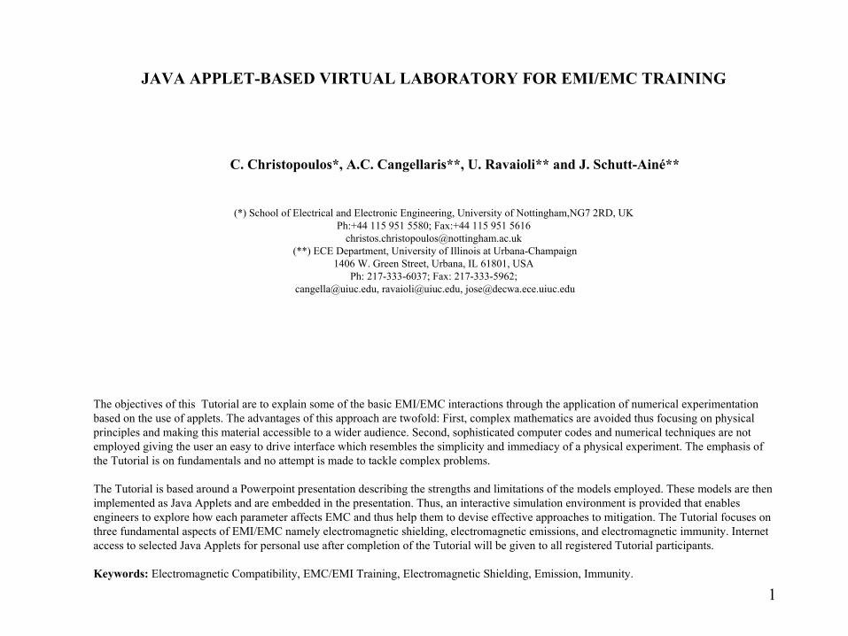
The central aim of this unit is to:
Understand the penetration of external incident EM fields throughapertures on equipment cabinets and calculate the Shielding
Effectiveness (SE). SE is the same whether one considersimmunity or emission.
H
E
k
external incident field
equipment cabinetaperture
?Estimate the amount by which the cabinet/aperture
attenuates the external incident field !
11
•General Objectives:
•establish the basic modelling methodology for understandingfield penetration through apertures
•study the impact of cabinet dimensions on SE.
•study the impact of aperture dimensions and number ofapertures on SE.
•quantify the influence of the cabinet contents on SE
•Establish design rules for SE

6
12
•Basic Concepts:
•A simple type of EM wave which can help us understand thebehaviour of more complex waves is the uniform plane wave.For this type of wave the electric E and magnetic H fieldcomponents are perpendicular to each other and to thedirection of propagation k.
k
E
Hy
x
z
In this example the electricfield has only an x-component, the magneticfield a y-component and thepropagation direction isalong z.
13
•More complex waves may be often analysed in terms of planewaves. All the essential concepts can be illustrated by focusingon plane waves.•The worst case as far as penetration is concerned is when theelectric field is perpendicular to the longest dimension of theaperture. This is easy to understand:
E E
Here the electric field is parallel to the walls of the slot, but the tangential component of the electric field should be
zero on a conducting surface-hence the field finds itdifficult to penetrate
Here the field fits exactlythe boundary conditions-hence
it penetrates easily

7
14
•The aperture (the slot in this case) will allow certain frequenciesto penetrate relatively easily while energy at other frequencies willpenetrate with difficulty. Intuition indicates that frequencies withwavelengths larger that the largest physical dimension of the slotwill not penetrate easily.
•As stated above, penetration through the slot is frequency-dependent. In addition, since the cabinet resonates at certainfrequencies, the EM energy which has penetrated past the slot willdistribute unevenly at different frequencies according to theresonant properties of the cabinet. The presence of PCBs andother components inside the cabinet complicates matters stillfurther. A formula for resonances in an empty box is given next.
15
•All these factors must taken into account in any model used topredict SE
2 2 2150MHz
m n pfa b d
Ê ˆ Ê ˆ Ê ˆ= + +Ë ¯ Ë ¯ Ë ¯
Resonance frequencies of an empty rectangular boxwith conducting walls and without apertures:
Where, the frequencies are in MHz, (a,b,d) are the internaldimensions of the box in meters, and (m,n,p) are integerswhich specify the particular mode or resonance. No morethan one of these integers can be zero. Each integers givesthe number of half wavelengths fitting in each direction.

8
16
•The Shielding Effectiveness (SE) is defined as the ratio indecibels of the incident electric field E0 without the cabinet, to thefield with the cabinet present Ec. In both cases the field iscalculated or measured at the same point.
020log( )c
ESEE
=
E
H
k
H
k
OBSERVATION POINT
E0
Ec
incident field
17
d
a
b wz
Output point
EMI source
boxaperture
Basic configuration:

9
18
•Detailed Model Development
The basic strategy is to derive simplified models of the slot(slotline) and of the cabinet (short-circuited waveguide) andcombine them to study penetration and coupling .
Each part in this interaction is modelled in the simplest possibleway. The following parts need to be modelled:
•The incident field
•The aperture/slot
•The cabinet
We develop models for each of the above part in turn.
19
Model for the Incident Field:
As far as the cabinet is concerned, the incident field can bedescribed by a Thevenin equivalent circuit where the voltagesource is V0, and the impedance is the intrinsic impedance of themedium (377 Ohm in air). The exact value of V0 is not importantfor SE calculation as it cancels out when the ratio of the two fieldsis formed.
V0
0h

10
20
Model for the Aperture:
w bA
AAt
/ 2 / 2
aperture
We will construct an equivalent circuit for the aperture as seenacross its centre (points A-AA).
Propagation along the aperture is similar to propagation along acoplanar stripline. There are in fact two such lines each of lengthl/2, which are, to the left and to the right, terminated by short-circuits (the front walls of the cabinet). The characteristicimpedance of this line Zocs may obtained from the literature.
21
Hence, the equivalent circuit across points A-AA is:
Zocs Zocs
A
AA
s/c s/c
/ 2/ 2
ZIN ZIN
( )0
0
tan / 22 /
IN ocsZ jZwhere
bb p l
==
Hence, the equivalent slot impedanceis equal to the input impedanceslooking left and right in parallel: ( )0
1 tan / 22slot ocsZ jZa
b=
Zslot
Scaling factor l/a accounts for the different length of slot and cabinet.Formulae for Zocs are given in the
appendix at the end of this presentation.

11
22
Model for the Cabinet:
a
bx
zƒy
We consider the cabinet as a rectangular waveguide withpropagation along z. The cutoff wavelength is
2c anl = n is and integer and we choose n=1 to get the
lowest possible cutoff frequency
The guide wavelength is then: ( )1g
c
l
l
ll
=-
23
This corresponds to waves bouncing between the sidewalls withno variation in x and n number of half sinusoidal variations in they-direction ( TE0,n mode). The guide characteristic impedance is:
meh
ll
Ê ˆ- Á ˜Ë ¯
=2
1g
cChoosing n=1 (lowest frequency mode) and expressingthe guide quantities in terms of the dimensions, we get:
( )0
21 2
g
a
hhl
=- ( )20 1 2g a
lb b= -
0 0 2, 377 ,where ph b l= W =

12
24
Hence, the model for the cabinet looks as follows:
,g gh b
Short-circuit at the wall opposite the aperture
To slotmodel
d
25
Complete model of the System:
We now put together all the various elements to form thecomplete model of the system:
Zslot
V0
0h,g gh b s/c
d
z
V(z)
In this model, the field inside the cabinet and at a distance z fromthe side with the slot is represented by the voltage V(z).

13
26
,g gh b s/c
d
z
V(z)
Vs
Zs
00
0 0,slot slot
s sslot slot
Z ZV V ZZ Z
hh h
= =+ +
The incident field and the slot models may be combined to form aThevenin equivalent as shown below;
This is now a standard TL circuit which can be solved for V(z).
27
,g gh b s/c
d
z
V(z)Vs
Zs
LEFT RIGHT
To simplify calculations, we replace the circuit to the LEFT and tothe RIGHT of the output point at z by their Thevenin equivalents:

14
28
RIGHT
V(z)
LEFTV1
Z1
Z2
( ) ( )1
cos sinss
g gg
VV Zz j zb bh
=+
( )( )
1tan
1 tan
s g g
sg
g
Z j zZ Zj z
h b
bh
+=
+
( )2 tang gZ j d zh bÈ ˘= -Î ˚
Thevenin equivalent at a distance z from the slot:
29
The voltage at z representing the electric field inside the box is then:
21
1 2( ) ZV z V
Z Z=
+
In the absence of the box the field is given by the followingequivalent:
V0
0h0h
Vnc 0 / 2ncV V=
Hence, the shielding effectiveness of the cabinet at point z is:
0 020log 20log2 ( )c
E VSEE V z
Ê ˆ Ê ˆ= = Á ˜Á ˜ Ë ¯Ë ¯

15
30
•Model Extensions
The procedure outlined shows how to obtain the electric fieldshielding effectiveness for an empty (unloaded) cabinet. Themagnetic field shielding effectiveness may also simply beobtained by calculating the ratio of currents rather than voltagesat point z.
We now investigate two additional aspects of shieldingeffectiveness which affect the behaviour of practical systems:
•loaded cabinets
•multiple apertures
These two extensions to the theory are dealt with by modifyingthe standard TL model described for the unloaded cabinet.
31
Loaded cabinet:
A simple, phenomenological, way to take account of the contentsof the cabinet and their impact on SE is to assume that thewaveguide representing the cabinet is lossy. In its simplest formthis model assumes distributed losses and a correction term ζthus replacing the guide characteristic impedance Zg andpropagation constant βg by
h z z h b z z b= + - = + -¢ ¢(1 ) , (1 )g g g gj j
The correction factor is of the order of the inverse of the loadedcabinet Q-factor
1 1Qz -
The use of the correction factor is explained in “Immittancetransformation using precision air-dielectric coaxial lines andconnectors” D. Woods, Proc. IEE, Vol. 118, 1971, pp. 1667-1674

16
32
Multiple apertures:
( )01 tan / 22slot ocsZ n jZa
b=
If there are n identical apertures then the equivalent slotimpedance is:
Circular apertures:
If the aperture is circular of diameter dh then to a goodapproximation the previous formulae may be used if we set
2 hw dp= =
33
•Applet-based Experimentation for SE•Show how the size and shape of the cabinet affects SE
•Show how the size and shape of the slot affects SE
•Learn about the particular behaviour of SE near cabinetresonances
•Understand the merits of using a larger number of smaller slotsto increase SE
•Assess how the contents of a cabinet affect SE especially nearresonances

17
34
Semi-empirical formula for SE*:
* H.W. Ott, “Noise Reduction Techniques in Electronic Systems”,2nd edition, Wiley 1988
A simple approximate formula used often to estimate the SE of acabinet with a slot is
20log2
SE lÊ ˆ= Ë ¯
This formula does not take into account the width of the slot orthe dimensions of the cabinet and therefore gives at best veryapproximate results. SE curves obtained using this formula areplotted for comparison with the results of the more sophisticatedmodel shown here (see numerical experiments that follow).
35
Using the Applet you can estimate the shielding effectiveness of acabinet:
See an example of this applet
in the next slide!
You will need to specify the following-
•dimensions of the cabinet
•dimensions of the slot
•position of the output point z (SE will be different depending onwhere the field is measured inside the box

18
36
37
Completion of this exercise should have given you an insightinto the following:
•the way in which cabinet size and shape affect SE
•the way in which slot size and shape affect SE
•the frequencies at which SE is at its lowest
•the configuration of slots that gives maximum SE
•effect of loading inside the cabinet on SE
•practically achievable values of SE at different frequencies
•distribution of field inside the cabinet

19
38
APPENDIX: Formulae for Zocs
Formulae for the characteristic impedance of a coplanarmicrostrip line may be found in , “Microstrip Lines and Slotlines”,K.C. Gupta, R. Garg, I. J. Bahl, Artech House,1979 (chapter 7).
They are summarised below: ( ) ( )120 / / /ocs e eZ K w b K w bp= ¢Where, K and K’ are elliptic integrals and we is the effective width
5 41 ln4et ww w
tp
pÈ ˘Ê ˆ= - +Í ˙Ë ¯Î ˚
Approximate formula: 124
224
1 1 ( / )120 ln 2
1 1 ( / )
/ 2
eocs
e
e
w bZw b
for w b
p
-È ˘Ê ˆ+ -Í ˙= Á ˜Á ˜Í ˙- -Ë ¯Î ˚
<
39
FURTHER READING:
1. “Shielding effectivenessof a rectangular enclosure with arectangular aperture”, M.P. Robinson et al, ElectronicsLetters, 15 Aug. 1996, Vol.32, No 17, pp.1559-1560
2. “Analytical evaluation of the shielding effectiveness ofenclosures with apertures”, M.P. Robinson et al, IEEETrans. on EMC, Vol. 40, No 3, 1998, pp.240-248
3. “Assessment of the shielding effectiveness of a real enclosure”, R. De Smedt et al, Int. Symp. On EMC, Sept.14-18, Rome, Italy, pp. 248-253
4. “Numerical and experimental study of the SE of a metallicenclosure”, F. Olyslager et al, IEEE Trans. On EMC, Vol.41, No 3, 1999, pp. 202-213

20
40
ELECTROMAGNETIC EMISSIONS
•Introduction and Aims•General Objectives
•Basic Concepts•Wire Interconnects as Radiating Antennas
•Applet-based Experimentation for Emissions•Further Reading
41
A basic electromagnetic interaction (EM) affecting EMC/SQ iswhen signals on wire interconnects or other componentsgenerate fields which couple to adjacent circuits or whichpropagate by radiation over large distances to couple to othercircuits.
Depending on the magnitude and spectral content of theseradiated fields circuits may malfunction and/or be permanentlydamaged.
Investigations into the level of radiated fields from circuits aredescribed under the term emission studies.
The reverse problem whereby a circuit is the victim to EM energyis referred to as a susceptibility/immunity study.
In this unit we focus on emission studies.
•Introduction and Aims

21
42
Radiation of EM energy from a wire interconnect may be studiedin connection with :
•impact on adjacent wires/circuits
•general pattern of radiated fields
The first case is normally studied under the heading of cross-talk(implying near-filed coupling described by mutualcapacitance/inductance). It is relevant to intra-system EMC.
The second case implies radiation some times over largedistances and therefore near-field and far-field radiation fromcircuits acting very much like antennas. It is relevant to inter-system EMC.
Both processes are important and often the boundaries betweenthem are not easy to establish.
However, the methodology of dealing with these two cases isdifferent and hence it is profitable to tackle each case separately.
In this unit we deal with the second case of general radiated fieldpatterns.
43
The central aim of this unit is to:
Understand the radiation of EM fields from wire interconnects andcalculate, in simple cases,the radiated field patterns.
Radiated EMI
V
I
voltages andcurrentsflowing in theinterconnect
Wire interconnect
22
44
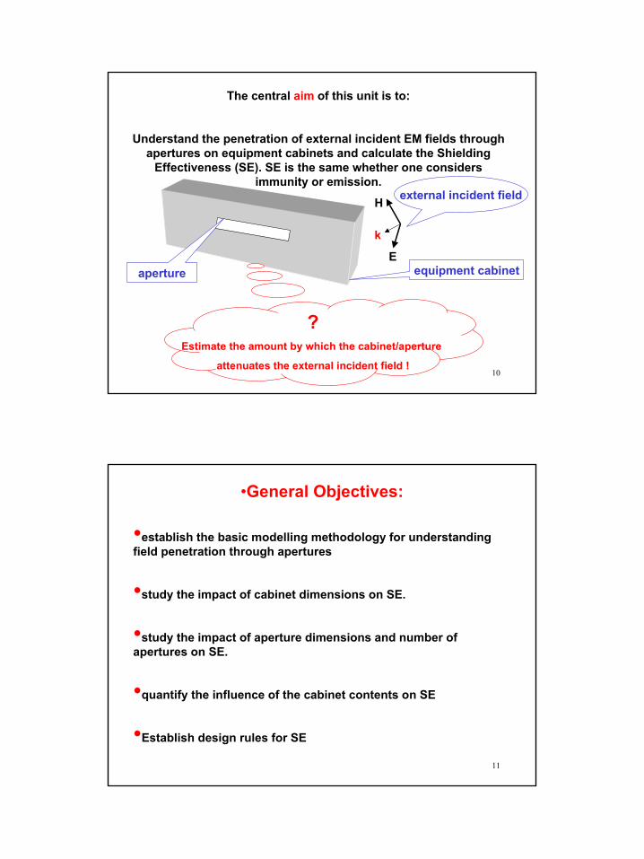
•General Objectives
•establish the basics for understanding radiated emissions fromsimple wire interconnects
•study the patterns of radiation from interconnects
•study the impact of line length, configuration, presence ofconducting planes and of terminations
•Discuss emissions from more complex configurations
45
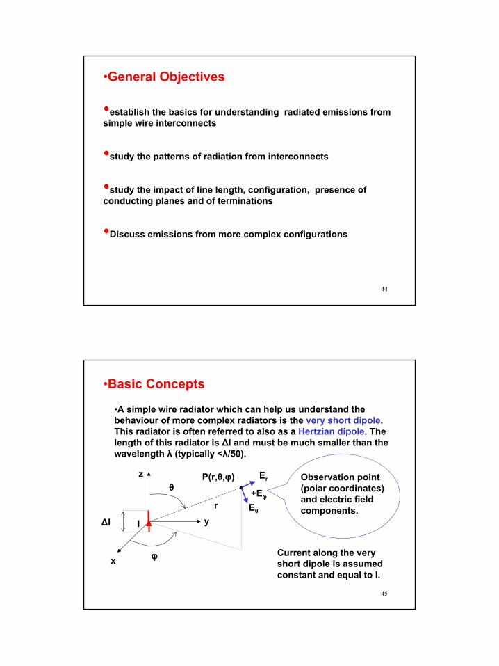
•Basic Concepts
•A simple wire radiator which can help us understand thebehaviour of more complex radiators is the very short dipole.This radiator is often referred to also as a Hertzian dipole. Thelength of this radiator is ∆l and must be much smaller than thewavelength λ (typically <λ/50).
Observation point(polar coordinates)and electric fieldcomponents.
x
y
z
∆l
θ
φ
r
I
P(r,θ,φ) Er
Eθ
+Εφ
Current along the veryshort dipole is assumedconstant and equal to I.

23
46
The field components at a point a distance r away from a veryshort dipole are given by the formulae:
2
2
1 1( ) sin 14 ( )
1 1( ) cos2 ( )
0
j r
j r
r
j eE I lr j r j r
j eE I lr j r j r
E
β
ϑ
β
ϕ
ωµ ϑπ β β
ωµ ϑπ β β
−
−
= ∆ + +
= ∆ +
=
0
( ) 1sin4
rj r
H HI l eH j
r r
ϑ
β
ϕ ϑ βπ
−
= =
∆ = + 2,where πβ λ=
47
We see that emissions, even from this simple structure displaycomplex behaviour, depending on r and θ. Also several termsappear which vary as 1/r, 1/r2, 1/r3.
At large distances (several wavelengths) only the 1/r termsremains and the emitted field has practically only two non-zerocomponents Eθ and Hφ. We are then at the far-field region.
( ) sin4
( ) sin4
, 377
j r
j r
I l eE jr
I l eH jr
where
β
ϑ
β
ϕ
βη ϑπ
β ϑπ
η
−
−
∆
∆
≡ ΩIntrinsic impedance of free space
24
48
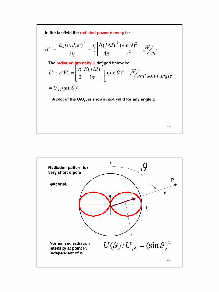
In the far-field the radiated power density is:
2 2 2
22
( , , ) ( ) (sin ) ,2 2 4r
E r I l WW mrϑ ϑ ϕ η β ϑ
η π∆
= =
The radiation intensity U defined below is:2
2 2
2
( ) (sin ) ,2 4
(sin )
r
pk
I l WU r W unit solid angle
U
η β ϑπ
ϑ
∆≡ =
=
A plot of the U/Upk is shown next valid for any angle φ.
49
P1
0Un
thn
ϑ
1
2( ) / (sin )pkU Uϑ ϑ=Normalised radiationintensity at point P,independent of φ.
r
Radiation pattern forvery short dipole
I
φ=const.

25
50
•Wire Interconnects as Radiating AntennasThe voltage and current distribution on an open-circuittransmission line is similar to that found on open-ended antennas.It therefore follows that we can learn a lot about emissions fromwire interconnects by studying the properties on antennas.
We will do this first to gain a broad appreciation of the emissionproperties of wires before looking at systematic computer-basedways of computing emissions.
∼
Open-ended antennacurrent distribution is a
standing wave pattern
Travelling-wave antennacurrent distribution can be
a travelling wave pattern
Antennatypes
51
•A standing wave pattern can be constructed as thesuperposition of travelling waves propagating in oppositedirections.
•In a travelling wave antenna where there is a single travellingwave, the amplitude of the wave is constant and the phase islinearly varying.
•In an open-ended (resonant) antenna the amplitude varies butthe phase is constant.
•The pattern of emission depends on the mix of travelling waveson the radiating structure.
26
52
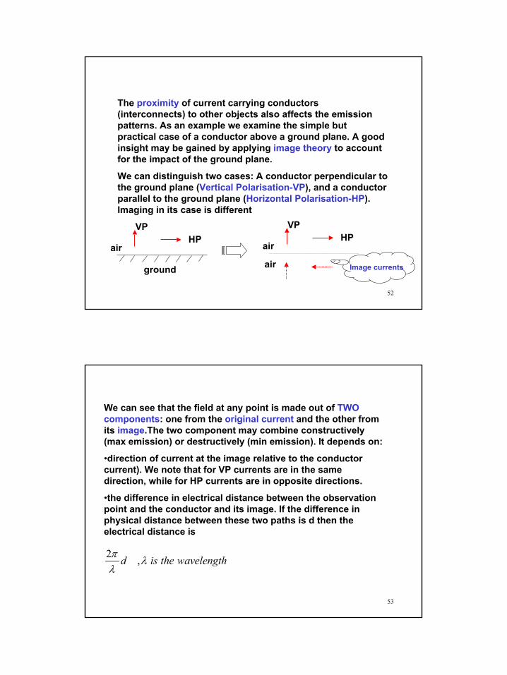
The proximity of current carrying conductors(interconnects) to other objects also affects the emissionpatterns. As an example we examine the simple butpractical case of a conductor above a ground plane. A goodinsight may be gained by applying image theory to accountfor the impact of the ground plane.
We can distinguish two cases: A conductor perpendicular tothe ground plane (Vertical Polarisation-VP), and a conductorparallel to the ground plane (Horizontal Polarisation-HP).Imaging in its case is different
VPHP
ground
air
VPHP
air
air Image currents
53
We can see that the field at any point is made out of TWOcomponents: one from the original current and the other fromits image.The two component may combine constructively(max emission) or destructively (min emission). It depends on:
•direction of current at the image relative to the conductorcurrent). We note that for VP currents are in the samedirection, while for HP currents are in opposite directions.
•the difference in electrical distance between the observationpoint and the conductor and its image. If the difference inphysical distance between these two paths is d then theelectrical distance is
2 ,d is the wavelengthπ λλ

27
54
The strength of the emitted field at the observation point willtherefore depend on whether we have VP or HP and on thefrequency as it affects directly electrical distance and thereforephase. This explains why in EMC measurements we do heightscans at each frequency etc.
In complex practical systems it can be difficult to predictemissions without resort to computational models. However, inorder to get a better understanding, we will present here threedifferent models of increasing levels of complexity
•emissions from single wires where there is a mix of forward andbackward travelling current waves
•emission from wires driven by asymmetrically placed sources
•emissions from complete circuits where the current is knownfrom numerical or other studies
55
Emissions from single wires where there is a mix of forward andbackward travelling current waves
Forward propagating current wave IFBackward propagating current wave IB
Observationpoint in the farfield region
ϑIF
IB
The configuration we examineis a wire with forward andbackward waves a shown. Weplot the radiation pattern.

28
56
0
7.5
15
22.5
30
37.5
45
52.560
67.57582.59097.5105
112.5120
127.5
135
142.5
150
157.5
165
172.5
180
187.5
195
202.5
210
217.5
225
232.5240
247.5255 262.5 270 277.5 285
292.5300
307.5
315
322.5
330
337.5
345
352.5
0.3
0.27
0.24
0.21
0.18
0.15
0.12
0.089
0.06
0.03
0
0.298
0En
thn
•Only forward wave (IB=0)
•Ratio of wire length towavelength is 5
•Maximum radiation in theforward direction at about 22degrees
57
0
7.5
15
22.5
30
37.5
45
52.560
67.57582.59097.5105
112.5120
127.5
135
142.5
150
157.5
165
172.5
180
187.5
195
202.5
210
217.5
225
232.5240
247.5255 262.5 270 277.5 285
292.5300
307.5
315
322.5
330
337.5
345
352.5
0.31
0.28
0.25
0.22
0.19
0.15
0.12
0.093
0.062
0.031
0
0.309
0En
thn
•As before,but forward andbackward current wavesare equal

29
58
0
7.5
15
22.5
30
37.5
45
52.560
67.57582.59097.5105
112.5120
127.5
135
142.5
150
157.5
165
172.5
180
187.5
195
202.5
210
217.5
225
232.5240
247.5255 262.5 270 277.5 285
292.5300
307.5
315
322.5
330
337.5
345
352.5
0.3
0.27
0.24
0.21
0.18
0.15
0.12
0.091
0.061
0.03
0
0.304
0En
thn
•As before, but backwardcurrent is 50% of theforward current
59
Emission from wires driven by asymmetrically placed sources
The problem we tackle here has two aspects (see ref. [3]):
• first, we work out the current distribution along a wire drivenby a sinusoidal source anywhere along its length
•second, based on this current distribution, we work out theemitted field
We can then plot I(z) and E(θ)z =
sz z=
0z =
∼
I(z)radius=a
r0E(θ)
V0

30
60
4
0
/ 100.33151.0
s
azkV Volts
−====
0 0.2 0.4 0.6 0.8 10
0.38
0.75
1.13
1.5
1.88
2.25
2.63
32.701
0
modn
IIk
10.01 znn zzk,/z
( )I zin mA
0
3.140.63
km
r m
===
0
30
60
90
120
150
180
210
240
270
300
330
0.0353
0.0309
0.0265
0.0221
0.0177
0.0132
0.0088
0.0044
0
0.035
0Ethetan
thetan
,VE mϑ
61
Emissions from complete circuits where the current is knownfrom numerical or other studies
( , , )n n n nI x y z
, ,( )n rE ϑ ϕ nn
E E= ∑
( , , )r ϑ ϕ
If the current distribution(CM and DM) isknown, then:
•separate wires into very short segments
•from each segment calculate emittedfield (very short dipole formula)
•use superposition to find total emittedfield

31
62
See an example ofthis applet in thenext slide!
•Applet-based Experimentation for Emissions
63

32
64
Completion of this exercise should have given you an insightinto the following:
•the way in which terminations affect emission
•the way in which line length and spacing affect emissions
•the directional patterns of emission from interconnects
•the impact of ground planes on emissions
65
•FURTHER READING
1. “Analysis of Multiconductor Transmission Lines”, C. R.Paul, Wiley 1994, (chapters 4,5)
2. “Principles and Techniques of Electromagnetic Compatibility”, C. Christopoulos, CRC Press 1995, (chapters 7,8)
3. “EMC Analysis Methods and Computational Models”, F.M. Tesche, M. V. Ianoz and T. Karlsson, Wiley 1997, (chapter 4)
4. “Antenna Theory: Analysis and Design”, C A Balanis,Wiley 1997 2nd Edition (Chapter 10)
5. “Control and Measurement of Unintentional EM Radiation”, W Scott Bennett, Wiley 1997

33
66
Electromagnetic Immunity
•Introduction and Aims•General Objectives•Basic Concepts•Model Formulation
•Models and Applet-basedexperimentation for Immunity
•Further Reading
67
A basic electromagnetic interaction (EM) affecting EMC/SQ iswhen an EM field couples to wires (i.e. induces voltages/currentson wire interconnects between circuits).
Depending on the magnitude and spectral content of theseinduced signals circuits may malfunction and/or be permanentlydamaged.
Investigations into the level of induced signals and the likelybehaviour of circuits are variously described as susceptibility orimmunity studies.
The reverse problem whereby the circuit emits EM energy isreferred to as emission study.
In this unit we focus on susceptibility/immunity studies.
•Introduction and Aims

34
68
Coupling of EM energy into a wire interconnect may be caused by:
•adjacent wires/circuits
•EM fields from distant wires/circuits
The first case is normally studied under the heading of cross-talk(implying near-filed coupling described by mutualcapacitance/inductance). It is relevant to intra-system EMC.
The second case implies interaction of circuits with an incidentfield (often a plane wave) representing far-field radiation fromdistant circuits acting very much like antennas. It is relevant tointer-system EMC.
Both processes are important and often the boundaries betweenthem are not easy to establish.
However, the methodology of dealing with these two cases isdifferent and hence it is profitable to tackle each case separately.
In this unit we deal with the second, far-field case.
69
The central aim of this unit is to:
Understand the coupling of external incident EM fields into wireinterconnects and calculate, in simple cases, induced voltages
and currents at circuit terminals.
Sourceof EMI
V
I
Inducedvoltagesandcurrents
Wire interconnect

35
70
•General Objectives
•establish the basic modelling methodology for understandingfield-to-wire coupling
•study the impact of field polarisation and propagation directionon coupling
•study the impact of line length, configuration, presence ofconducting planes and of terminations
•establish basic guidelines to reduce field-to-wire coupling
71
•Basic Concepts
•A simple type of EM wave which can help us understand thebehaviour of more complex waves is the uniform plane wave.For this type of wave the electric E and magnetic H fieldcomponents are perpendicular to each other and to thedirection of propagation k.
k
E
Hy
x
z
In this example the electricfield has only an x-component, the magneticfield a y-component and thepropagation direction isalong z.

36
72
•Polarisation of the electric field refers to the direction of theelectric field relative to the configuration of the line (e.g. electricfield vector parallel to the line, transverse to the line, or, in someother direction). Physical intuition suggests that polarisationaffects the strength of coupling.
•Direction of propagation refers to the direction in which EMenergy is transported in space by the wave. Clearly, the directionof incidence of EM energy on the line will affect coupling. Seebelow some simple wave propagation directions for exciting aline :
line ƒ
Arrows show direction of propagation k:
Broadside excitation
Endfire excitation
Sidefire excitation
E
73
•Line terminations refers to the loads at the two ends of a wireinterconnect. As an EM waves impinges on the line the inducedcurrents and voltages and wave reflections will depend on theterminations
•TEM conditions in wire interconnects refer to the situation wherethe electric and magnetic field between the wires have onlytransverse components to the direction of propagation (strictlytrue only for lossless lines)
•Conducting planes in the vicinity of the interconnect, or as a partof it, may affect coupling e.g. by causing reflections to incidentwaves.
37
74
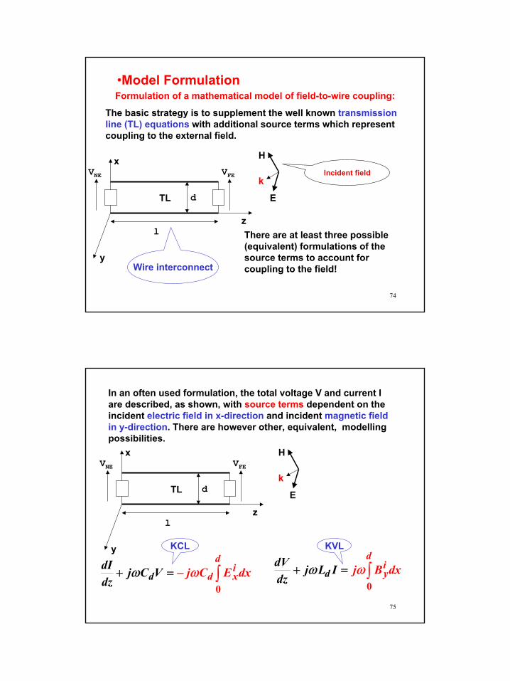
Formulation of a mathematical model of field-to-wire coupling:
The basic strategy is to supplement the well known transmissionline (TL) equations with additional source terms which representcoupling to the external field.
x
y
z
TL
l
d
VFEVNEH
E
kIncident field
There are at least three possible(equivalent) formulations of thesource terms to account forcoupling to the field!Wire interconnect
•Model Formulation
75
x
y
z
TL
l
d
VFEVNEH
E
k
w w+ = Ú0
d
ydidV j L jI
dzB dxw w= -+ Ú
0
di
d xd jdI j EC V dxdz
C
In an often used formulation, the total voltage V and current Iare described, as shown, with source terms dependent on theincident electric field in x-direction and incident magnetic fieldin y-direction. There are however other, equivalent, modellingpossibilities.
KCL KVL

38
76
The main alternative model formulations are in terms of sourceterms depending on the incident, electric field only, or, themagnetic field only.
For a critical discussion of the various models and theirequivalence see:
“On the contribution of the EM field components in field-totransmission line interaction”
C.A. Nucci and F. Rachidi, IEEE Trans. On EMC, 37, No. 4, Nov.1995, pp. 505-508.
The model as shown is formulated in the frequency-domain(time is not the independent variable, harmonic excitations offrequency f are assumed). If a pulsed field is applied it mustfirst be analysed into its frequency components, the lineresponse to each component found by solving the previousequations, and the results combined to obtain the totalresponse (only possible for linear systems).
77
Alternatively, the model may be formulated in the time-domain toobtain a more direct solution for the effects of pulsed fields on theline which is also valid for general non-linear systems.
Both, frequency- and time-domain approaches are used informulating models which can be solved either analytically (forsimple cases) ,or, numerically.
Analytical solutions are possible for many cases especially at low-frequencies where neglecting transmission line effects simplifiesthe equations. Although low-frequency results cannot be used athigh frequencies they nevertheless provide an insight into basiccoupling mechanisms which is invaluable to the designer.

39
78
Numerical solutions are obtained by dividing the line into manysmall segments, each smaller than a wavelength, and inserting ineach segment voltage and current sources which represent thecoupling to the electric and magnetic field componentsrespectively, as explained earlier. This process is illustratedbelow:
Ld∆z
Cd∆z
Vs∆z
Is∆z
+
∆z
w= Ú0
( ) ( , )s
diyz j xV B z dx
w= - Ú0
( ) ( , )d
id xs z j C xI E z dx
Parameters of the TL segment
Source terms
79
There are THREE types of solutions to the coupling models:
Simple model
This is a low-frequency model where all excitation sources arelumped together, the inductance and capacitance of the line isneglected and the near-end and far-end impedances are assumedto be approximately equal to the characteristic impedance of theline. This model is sketched out below.
+Vsrc
IsrcVNE VFERs Rl

40
80
TEM model
This a model valid up to medium frequencies and it is based onsolving the TL equations assuming TEM approximation (linelength much larger than separation, no losses). This solution canbe done in either the frequency or time domains. Here, thefrequency-domain solution is used.
High-frequency model
A high-frequency field model valid for all frequencies includinglines with substantial losses and arbitrary separation. Here asolution based on the Method of Moments (MoM) must be used.This model is beyond the scope of this presentation.
81
We now look at some specific examples to get some intuitiveunderstanding and quantitative information regarding coupling towires.
There are three basic interconnect configurations:
•A parallel wire interconnect
•A wire-above-ground interconnect
•A parallel wire interconnect above ground
For each configuration we apply one or more of the three differentmodels described (Simple, TEM and High-frequency models).
Examples of sidefire, broadside and endfire excitations arestudied.

41
82
•Show how the length, spacing,and line terminations affectinduced voltages
•Establish the range of validity of the different models
•Learn about the inaccuracies of coupling predictions based onthe assumption of electrically very short lines
•Study the behaviour of an electrically long line that radiatessubstantially (requires high-frequency model)
•Compare the severity of coupling due to different excitationmodes (sidefire, broadside and endfire). Establish worst case andsuggest possible remedies.
•Models and Applet-based Experimentationfor Immunity
83
objectives (cont.):
•Compare coupling for parallel wire, wire-above-conductingplane, and parallel wires above conducting plane lines
•Establish the circumstances when a full-field solution for theinterconnect configuration is necessary
•Based on the numerical experiments you have done, suggestbroad design guidelines to minimise coupling from external fieldsto wire interconnects

42
84
NEV FEV
x
z
y
dsZ
Z
iHiE
k⊗
sidefire
SIDEFIRE Excitation:The configuration studied is shown below. The line length is and the spacing is d. The near-end (NE) and far-end (FE)quantities are shown, together with the correspondingterminations Zs and Z .
85
For this excitation the electric filed has only a z-component andthe magnetic field a y-component. Using these field componentsthe equivalent sources are calculated and inserted into the field-to-wire coupling model described earlier.
Basic transmission line theory is then used to obtain solutions forthe terminal voltages at the line terminations.
The following information is required:
•magnitude of the electric field component E0 .The magnetic fieldneed not be explicitly supplied as for a plane wave
where η is the intrinsic impedance of the medium. In air,
h= /H E
mh h e= = = W00 0377

43
86
•the frequency of the excitation f. This permits the calculation ofthe line phase constant,
•vp is the velocity of propagation on the line. We assume alossless line.
•the geometrical and material properties of the line. These allowthe calculation of the per unit length capacitance and inductanceof the line, its characteristic impedance, velocity of propagationetc.
•the impedance of line terminations. For simplicity, we assumethat the impedances at terminations are resistive.
b p l w= =2 / / pv
In the next slides we summarise the formulae used and in theWEB-based exercises for sidefire coupling
87
Simple model for sidefire coupling on parallel wire interconnect:
( ) ( )( )
( )bbbb
-È ˘= - -Í ˙+ Î ˚
/ 20
sin / 2/ 2
j dsNE
s
dZV j d E eZ Z d
[ ]FEs
ZV as aboveZ Z
=+
In these formulae :
b p l= -=
= +0
12 /, ( 0)NE FE
j
V V are phasors E E j

44
88
Advantages of the simple model:
•very easy to use, results obtained quickly
•clear physical understanding of parameters affecting coupling
Limitations of the simple model:
•line must be electrically very short (line length<<λ)
•excitation sources lumped together
•line L and C are neglected
•impedance at line terminations must be of the same order asthe line characteristic impedance
•re-radiation from the line is neglected
89
NEV FEV
x
z
y
hsZ
Z
iHiE
k⊗
sidefire
SIDEFIRE Excitation:The configuration studied is shown below. The line length is and the height is h. The near-end (NE) and far-end (FE)quantities are shown, together with the correspondingterminations Zs and Z .
Conducting plane
Wire-above conducting
plane configuration

45
90
Simple model for sidefire excitation in an wire-above-conducting-plane configuration:
( ) bbb
È ˘= - Í ˙+ Í ˙Î ˚
0sin( )2
( )s
NEs
Z hV j h EZ Z h
[ ]=+FEs
ZV as aboveZ Z
91
TEM model for the sidefire excitation of a parallel-wireinterconnect :
[ ]bbb b b- È ˘
= - +Í ˙Î ˚
sin( / 2)/ 20( / 2) cos( ) 1 sin( )dj d
NE s d c
E ZV Z de jD Z
[ ]b b b bb
- È ˘= - - +Í ˙Î ˚
/ 20 sin( / 2) cos( ) 1 sin( )( / 2)
j d sFE
c
E d ZV Z de jD d Z
where,
b b Ê ˆ= + + +Á ˜Ë ¯
cos( )( ) sin( ) ss c
c
Z ZD Z Z j ZZ

46
92
TEM model for the sidefire excitation of a wire-above-conducting-plane interconnect :
[ ]b b bb
È ˘= - - +Í ˙
Î ˚0 sin( )2 cos( ) 1 sin( )
( )NE sc
E h ZV Z h jD h Z
[ ]b b bb
È ˘= - +Í ˙Î ˚
0 sin( )2 cos( ) 1 sin( )( )
sFE
c
E h ZV Z h jD h Z
b b= + + +cos( )( ) sin( )( )ss c
c
Z ZD Z Z j ZZ
where,
93
See an exampleof this applet inthe next slide!
Find out how the length, spacingand line terminations affect thenear- and far-end voltages.
How do the simple and TEMmodels compare?
Sidefire excitation of aparallel-wire and wire-above-conducting-planeinterconnects.

47
94
95

48
96
NEV FEV
x
z
y
dsZ
Z
iH
iE
k ⊗broadside
Broadside Excitation:The configuration studied is shown below. The line length is and the spacing is d. The near-end (NE) and far-end (FE)quantities are shown, together with the correspondingterminations Zs and Z .
97
For this excitation, the electric field has only an x-component andthe magnetic field a z-component. The same approach andnotation as for the sidefire excitation is adopted.
Three models are employed and each has the same advantagesand limitations as for the sidefire case.
You should now look at the predictions of these models andobtain results to compare with the sidefire excitation.
Simple model for the broadside excitation of a parallel-wire line :
[ ]0( )sNE FE d
s
Z ZV V j C d EZ Z
w= = -+

49
98
NEV FEV
x
z
y
hsZ
Z
iH
iE
k ⊗broadside
BROADSIDE Excitation:The configuration studied is shown below. The line length is and the height is h. The near-end (NE) and far-end (FE)quantities are shown, together with the correspondingterminations Zs and Z .
Conducting plane
Wire-above conducting
plane configuration
99
Simple model of the broadside excitation of a wire-above-conducting-plane interconnect :
[ ]02( )sNE FE d
s
Z ZV V j C h EZ Z
w= = -+

50
100
TEM model for the broadside excitation of a parallel-wireinterconnect :
0 cos( ) 1 sin( )NE sc
dE ZV Z jD Z
b bÈ ˘= - - +Í ˙Î ˚
b bÈ ˘= - -Í ˙Î ˚
0 1 cos( ) sin( )sFE
c
dE ZV Z jD Z
where,
b b= + + +cos( )( ) sin( )( )ss c
c
Z ZD Z Z j ZZ
101
TEM model for the broadside excitation of a wire-above-conducting-plane interconnect :
02 cos( ) 1 sin( )NE sc
hE ZV Z jD Z
b bÈ ˘= - - +Í ˙
Î ˚
b bÈ ˘= - -Í ˙
Î ˚02 1 cos( ) sin( )s
FEc
hE ZV Z jD Z
where,
b b= + + +cos( )( ) sin( )( )ss c
c
Z ZD Z Z j ZZ
Now trythe applet!

51
102
NEV FEV
x
z
y
dsZ
Z
iH
iE
kendfire
ENDFIRE Excitation:The configuration studied is shown below. The line length is and the spacing is d. The near-end (NE) and far-end (FE)quantities are shown, together with the correspondingterminations Zs and Z .
103
For this type of excitation the electric field has an x-componentonly and the magnetic field a y-component. The relevant modelsare given below:Simple model of an endfire excitation of an interconnect:
= - ++ +s s
NE src srcs l s
Z Z ZV V IZ Z Z Z
= ++ +
sFE src src
s s
Z Z ZV V IZ Z Z Z
where,bb -= / 2
0( ) jsrcV j d E e
/ 20( ) j
src dI j C d E e bw -= -
For a parallel-wire interconnect
For a wire-above-conducting-plane interconnect replaced by 2h in the formulae for Vsrc and Isrc.

52
104
TEM model of endfire excitation of wire interconnect:
b È ˘= - +Í ˙
Î ˚0 sin( ) 1NE s
c
dE ZV jZD Z
[ ]b bÈ ˘= - - +Í ˙Î ˚
0 1 1 cos(2 ) sin(2 )2
sFE
c
dE ZV Z jD Z
cos( )( ) sin( ) ss c
c
Z ZD Z Z j ZZ
b b Ê ˆ= + + +Á ˜Ë ¯
where,
For parallel-wire
interconnect
For wire-above-conducting-plane interconnectreplace d by 2h in the above formulae.
105
Completion of these exercises should have given you an insightinto the following:
•the way in which line length affects coupling (i.e. resonances)•the way in which the loop area of the line (d ) affects coupling
•in what way the three excitations are different and whether thereis any merit in configuring the line in any particular way if theprimary EMI excitation threat is known
•the influence of terminations on severity of coupling for thedifferent excitations
•worst case coupling and best configuration/excitation formaximum immunity (design guidelines)
•range of applicability of the three modelsSimple model (low frequency), TEM model (medium frequency), High-frequencymodel

53
106
•Further Reading
1. “Analysis of Multiconductor Transmission Lines”, C. R.Paul, Wiley 1994, (chapter 7)
2. “Principles and Techniques of Electromagnetic Compatibility”, C. Christopoulos, CRC Press 1995, (chapter 7)
3. “EMC Analysis Methods and Computational Models”, F.M. Tesche, M. V. Ianoz and T. Karlsson, Wiley 1997, (chapter 7)
107
CONCLUDING REMARKS
•Many important EMC phenomena can bestudied by simple models
•Applets can be used to relieve the student fromexcessive calculation and to illustrate trends indesign
•Applet based material offers a virtual laboratoryaccessible from anywhere via the internet
•We plan to enhance and extend this work toprovide a sophisticated and effective learningenvironment