1. General description - NXP Semiconductors | …. General description The TDA8296 is an...
87
1. General description The TDA8296 is an alignment-free digital multistandard vision and sound low IF signal PLL demodulator for positive and negative video modulation including AM and FM mono sound processing. It can be used in all countries worldwide for M/N, B/G/H, I, D/K, L and L-accent standard. CVBS and SSIF/mono audio are provided via two DACs. FM radio preprocessing is included for simple interfacing with demodulator/stereo decoder backends. The IC is especially suited for the application with the NXP Silicon Tuner TDA1827x. All the processing is done in the digital domain. The chip has an ‘easy programming’ mode to make the I 2 C-bus protocol very simple. In principle, only one bit sets the proper standard with recommended content. However, if this is not suitable, free programming is always possible. Note: Register 06h has to be reprogrammed to new value C4h (see Section 9.2 and Section 9.3.1 ). 2. Features and benefits Digital IF demodulation for all analog TV standards worldwide (M/N, B/G/H, D/K, I, L and L-accent standard) Multistandard true synchronous demodulation with active carrier regeneration Alignment-free 16 MHz typical reference frequency input (from low IF tuner) or operating as crystal oscillator Internal PLL synthesizer which allows the use of a low-cost crystal (typically 16 MHz) Especially suited for the NXP Silicon Tuner TDA1827x No SAW filter needed Low application effort and external component count in combination with the TDA1827x Simple upgrade of TDA8295 possible 12-bit low power IF ADC on chip running with 54 MHz or 27 MHz Two 10-bit DACs on chip for CVBS and SSIF or audio Easy programming for I 2 C-bus High flexibility due to various I 2 C-bus programming registers I 2 C-bus interface and I 2 C-bus feed-through for tuner programming Four I 2 C-bus addresses selectable via two external pins TDA8296 Digital global standard low IF demodulator for analog TV and FM radio Rev. 1 — 3 March 2011 Product data sheet
Transcript of 1. General description - NXP Semiconductors | …. General description The TDA8296 is an...

1. General description
The TDA8296 is an alignment-free digital multistandard vision and sound low IF signal PLL demodulator for positive and negative video modulation including AM and FM mono sound processing. It can be used in all countries worldwide for M/N, B/G/H, I, D/K, L and L-accent standard. CVBS and SSIF/mono audio are provided via two DACs. FM radio preprocessing is included for simple interfacing with demodulator/stereo decoder backends.
The IC is especially suited for the application with the NXP Silicon Tuner TDA1827x.
All the processing is done in the digital domain.
The chip has an ‘easy programming’ mode to make the I2C-bus protocol very simple. In principle, only one bit sets the proper standard with recommended content. However, if this is not suitable, free programming is always possible.
Note: Register 06h has to be reprogrammed to new value C4h (see Section 9.2 and Section 9.3.1).
2. Features and benefits
Digital IF demodulation for all analog TV standards worldwide (M/N, B/G/H, D/K, I, L and L-accent standard)Multistandard true synchronous demodulation with active carrier regenerationAlignment-free16 MHz typical reference frequency input (from low IF tuner) or operating as crystal oscillatorInternal PLL synthesizer which allows the use of a low-cost crystal (typically 16 MHz)Especially suited for the NXP Silicon Tuner TDA1827xNo SAW filter neededLow application effort and external component count in combination with the TDA1827xSimple upgrade of TDA8295 possible12-bit low power IF ADC on chip running with 54 MHz or 27 MHzTwo 10-bit DACs on chip for CVBS and SSIF or audioEasy programming for I2C-busHigh flexibility due to various I2C-bus programming registersI2C-bus interface and I2C-bus feed-through for tuner programmingFour I2C-bus addresses selectable via two external pins
TDA8296Digital global standard low IF demodulator for analog TV and FM radioRev. 1 — 3 March 2011 Product data sheet
NXP Semiconductors TDA8296Digital global standard low IF demodulator for analog TV and FM radio
Gated IF AGC acting on black level by using H/V PLL or peak IF AGC (I2C-bus selectable)Internal digital logarithmic IF AGC amplifier with up to 48 dB gain and 68 dB control rangePeak search tuner IF AGC for optimal adaptive drive of the IF ADCSwitchable IF PLL and IF AGC loop bandwidthsPrecise AFC and lock detectorAccurate group delay equalization for all standardsVery robust IF demodulator coping with adverse field conditionsWide PLL pull-in range up to ±1 660 kHz (I2C-bus selectable)CVBS and SSIF or audio output with simple postfilter (capacitor only)CVBS gain levelling stage to provide nearly constant signal amplitude during over modulationVideo equalizer with eight settingsNyquist filter in video basebandExcellent video S/N (typically 60 dB weighted)High selectivity video low-pass filter for all standardsLow video into sound crosstalkSSIF AGCSound performance comparable to QSS single reference conceptsAM/FM mono sound demodulatorSwitchable de-emphasisExcellent FM soundGood AM soundHigh FM Deviation mode for ChinaPreprocessing of FM radio (mono and stereo) with highly selective digital band-pass filterNo ceramic filter or external components needed for FM radioFM radio available in monoAutomatic or forced mute for mono soundAutomatic or forced blank for videoMostly digital FIR filter implementation (NSC notches and video low-pass filters)Three GPIO pinsPower-On Reset (POR) block for reliable power-up behaviorVery low total power dissipation (typically 150 mW)No power sequence requirementStandby mode (typically 5 mW)40-pin HVQFN packageCMOS technology (0.090 μm 1.2 V and 3.3 V)
3. Applications
TV applicationsRecordingPC TV applications
TDA8296 All information provided in this document is subject to legal disclaimers. © NXP B.V. 2011. All rights reserved.
Product data sheet Rev. 1 — 3 March 2011 2 of 87
NXP Semiconductors TDA8296Digital global standard low IF demodulator for analog TV and FM radio
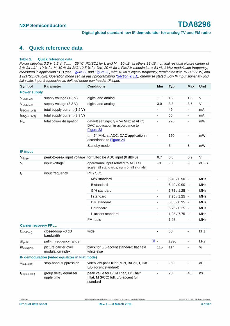
4. Quick reference data
Table 1. Quick reference data Power supplies 3.3 V, 1.2 V; Tamb = 25 °C; PC/SC1 for L and M = 10 dB, all others 13 dB; nominal residual picture carrier of 3 % for L/L’ , 10 % for M, 10 % for B/G, 12.5 % for D/K, 20 % for I; FM/AM modulation = 54 %, 1 kHz modulation frequency; measured in application PCB (see Figure 22 and Figure 23) with 16 MHz crystal frequency, terminated with 75 Ω (CVBS) and 1 kΩ (SSIF/audio). Operation mode set via easy programming (Section 9.3.1), otherwise stated. Low IF input signal at -3dB full scale, input frequencies as defined under row header IF input.
Symbol Parameter Conditions Min Typ Max UnitPower supplyVDD(1V2) supply voltage (1.2 V) digital and analog 1.1 1.2 1.3 V
VDD(3V3) supply voltage (3.3 V) digital and analog 3.0 3.3 3.6 V
IDD(tot)(1V2) total supply current (1.2 V) - 49 - mA
IDD(tot)(3V3) total supply current (3.3 V) - 65 - mA
Ptot total power dissipation default settings; fs = 54 MHz at ADC; DAC application in accordance to Figure 23
- 270 - mW
fs = 54 MHz at ADC; DAC application in accordance to Figure 24
- 150 - mW
Standby mode - 5 8 mW
IF inputVi(p-p) peak-to-peak input voltage for full-scale ADC input (0 dBFS) 0.7 0.8 0.9 V
Vi input voltage operational input related to ADC full scale; all standards; sum of all signals
−3 −3 −3 dBFS
fi input frequency PC / SC1
M/N standard - 5.40 / 0.90 - MHz
B standard - 6.40 / 0.90 - MHz
G/H standard - 6.75 / 1.25 - MHz
I standard - 7.25 / 1.25 - MHz
D/K standard - 6.85 / 0.35 - MHz
L standard - 6.75 / 0.25 - MHz
L-accent standard - 1.25 / 7.75 - MHz
FM radio - 1.25 - MHz
Carrier recovery FPLLB−3dB(cl) closed-loop −3 dB
bandwidthwide - 60 - kHz
Δfpullin pull-in frequency range [1] - ±830 - kHz
mover(PC) picture carrier over modulation index
black for L/L-accent standard; flat field white else
115 117 - %
IF demodulation (video equalizer in Flat mode)αsup(stpb) stop-band suppression video low-pass filter (M/N, B/G/H, I, D/K,
L/L-accent standard)- −60 - dB
tripple(GDE) group delay equalizer ripple time
peak value for B/G/H half, D/K half, I flat, M (FCC) full, L/L-accent full standard
- 20 40 ns
TDA8296 All information provided in this document is subject to legal disclaimers. © NXP B.V. 2011. All rights reserved.
Product data sheet Rev. 1 — 3 March 2011 3 of 87
NXP Semiconductors TDA8296Digital global standard low IF demodulator for analog TV and FM radio
CVBS outputVo(p-p) peak-to-peak output
voltagenegative PC modulation (all standards except L/L-accent); 75 Ω DC load; sync-white modulation; 90 % (nominal)
0.9 1.0 1.1 V
positive PC modulation (L/L-accent standard); 75 Ω DC load; sync-white modulation; 97 % (nominal)
0.9 1.0 1.1 V
Bvideo(−3dB) −3 dB video bandwidth overall video response; CVBS equalizer flat
all standards except M/N 4.7 4.85 - MHz
M/N standard 3.8 3.9 - MHz
αresp(f) frequency response video equalizer; 8 equally spaced settings; value at 3.9 MHz
−5 - +4.5 dB
Gdif differential gain “ITU-T J.63 line 330” - 1.5 5 %
ϕdif differential phase “ITU-T J.63 line 330” - 1.0 3 deg
(S/N)w weighted signal-to-noise ratio
all standards; unified weighting filter (“ITU-T J.61”); PC at −6 dBFS
57 60 - dB
SSIF/mono sound outputVo(SSIF)(RMS) RMS SSIF output voltage 1 kΩ DC or AC load; no modulation;
PC / SC1 = 13 dB
M standard 105 115 127 mV
B standard 97 104 116 mV
G/H standard 97 104 116 mV
D/K standard 89 96 106 mV
I standard 93 100 111 mV
L standard 89 96 106 mV
L-accent standard 89 96 106 mV
FM radio (single carrier) 94 103 115 mV
Vo(AF)(RMS) RMS AF output voltage 1 kΩ DC or AC load
M standard; 54 % modulation degree (±13.5 kHz FM deviation before pre-emphasis)
98 116 135 mV
B, G/H, I, D/K standard; 54 % modulation degree (±27 kHz FM deviation before pre-emphasis)
107 126 144 mV
αhr(AF) AF headroom before clipping; 1 kΩ DC or AC load
M standard; related to ±25 kHz peak deviation before pre-emphasis
- 7 - dB
B, G/H, I, D/K standard; related to ±50 kHz peak deviation before pre-emphasis
- 7 - dB
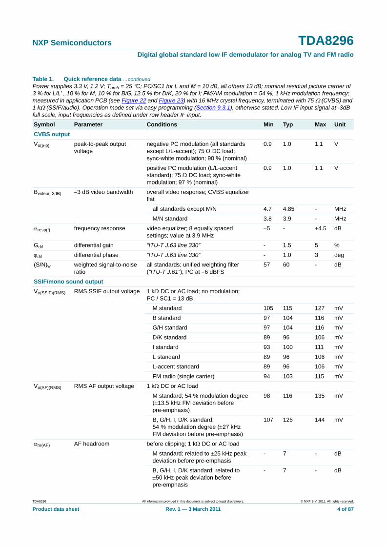
Table 1. Quick reference data …continuedPower supplies 3.3 V, 1.2 V; Tamb = 25 °C; PC/SC1 for L and M = 10 dB, all others 13 dB; nominal residual picture carrier of 3 % for L/L’ , 10 % for M, 10 % for B/G, 12.5 % for D/K, 20 % for I; FM/AM modulation = 54 %, 1 kHz modulation frequency; measured in application PCB (see Figure 22 and Figure 23) with 16 MHz crystal frequency, terminated with 75 Ω (CVBS) and 1 kΩ (SSIF/audio). Operation mode set via easy programming (Section 9.3.1), otherwise stated. Low IF input signal at -3dB full scale, input frequencies as defined under row header IF input.
Symbol Parameter Conditions Min Typ Max Unit
TDA8296 All information provided in this document is subject to legal disclaimers. © NXP B.V. 2011. All rights reserved.
Product data sheet Rev. 1 — 3 March 2011 4 of 87

NXP Semiconductors TDA8296Digital global standard low IF demodulator for analog TV and FM radio
[1] The pull-in range can be doubled to ±1 660 kHz by I2C-bus register like described in Table 16. Then the AFC read-out has 256 steps.
[2] To set audio gain to +6 dB for internal sound demodulation, register 22h has to be programmed to 08h.
5. Ordering information
THD total harmonic distortion FM; for 50 kHz deviation before pre-emphasis (25 kHz for M standard)
- 0.15 0.3 %
AM; m = 80 % - 0.5 1 %
BAF(−3dB) −3 dB AF bandwidth AM 20 27 - kHz
FM 40 50 - kHz
(S/N)w(AF) AF weighted signal-to-noise ratio
via internal mono sound demodulator; “ITU-R BS.468-4”; FM mode related to 27 kHz deviation before pre-emphasis; 10 % residual PC; SC1; color bar picture
52 54 - dB
via internal mono sound demodulator; (audio gain +6 dB) “ITU-R BS.468-4”; AM; m = 54 %; 3 % residual PC; SC1; color bar picture
[2] 40 44 - dB
Table 1. Quick reference data …continuedPower supplies 3.3 V, 1.2 V; Tamb = 25 °C; PC/SC1 for L and M = 10 dB, all others 13 dB; nominal residual picture carrier of 3 % for L/L’ , 10 % for M, 10 % for B/G, 12.5 % for D/K, 20 % for I; FM/AM modulation = 54 %, 1 kHz modulation frequency; measured in application PCB (see Figure 22 and Figure 23) with 16 MHz crystal frequency, terminated with 75 Ω (CVBS) and 1 kΩ (SSIF/audio). Operation mode set via easy programming (Section 9.3.1), otherwise stated. Low IF input signal at -3dB full scale, input frequencies as defined under row header IF input.
Symbol Parameter Conditions Min Typ Max Unit
Table 2. Ordering information Type number Package
Name Description VersionTDA8296HN HVQFN40 plastic thermal enhanced very thin quad flat package; no leads;
40 terminals; body 6 × 6 × 0.85 mmSOT618-1
TDA8296 All information provided in this document is subject to legal disclaimers. © NXP B.V. 2011. All rights reserved.
Product data sheet Rev. 1 — 3 March 2011 5 of 87
xxxx xxxxxxxxxxxxxxxxxxxxxxxxxxxxxx x xxxxxxxxxxxxxx xxxxxxxxxx xxx xxxxxx xxxxxxxxxxxxxxxxxxxxxxx xxxxxxxxxxxxxxxxxxxxxx xxxxx xxxxxx xx xxxxxxxxxxxxxxxxxxxxxxxxxxxxx xxxxxxxxxxxxxxxxxxxxxx xxxxxxxxxxx xxxxxxx xxxxxxxxxxxxxxxxxxx xxxxxxxxxxxxxxxx xxxxxxxxxxxxxx xxxxxx xx xxxxxxxxxxxxxxxxxxxxxxxxxxxxxxxx xxxxxxxxxxxxxxxxxxxxxxxx xxxxxxx xxxxxxxxxxxxxxxxxxxxxxxxxxxxxxxxxxxxxxxxxxxxxx xxxxxxxxxxx xxxxx x x
TDA8296
Product data sh
NXP Sem
iconducto
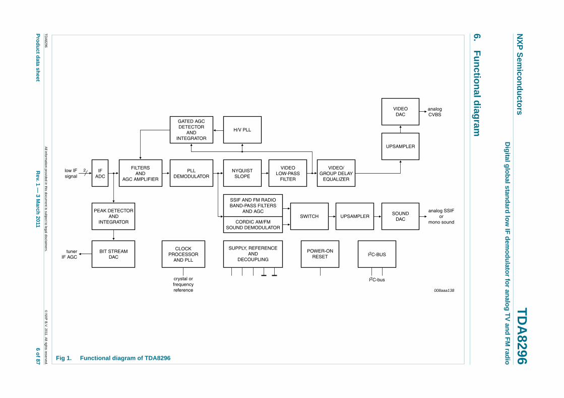
6. Functional d
eet
rsTD
A8296
Digital global standard low
IF demodulator for analog TV and FM
radio
iagram
008aaa138
analogCVBS
analog SSIFor
mono sound
C-bus
VIDEODAC
UPSAMPLER
C-BUS
SOUNDDAC
All information provided in this docum
ent is subject to legal disclaimers.
© N
XP B
.V. 2011. All rights reserved.
Rev. 1 —
3 March 2011
6 of 87 Fig 1. Functional diagram of TDA8296
2low IFsignal
tunerIF AGC
I2
GATED AGCDETECTOR
ANDINTEGRATOR
H/V PLL
VIDEO/GROUP DELAY
EQUALIZER
VIDEOLOW-PASS
FILTER
SWITCH
I2
UPSAMPLER
NYQUISTSLOPE
PLLDEMODULATOR
FILTERSAND
AGC AMPLIFIER
PEAK DETECTORAND
INTEGRATOR
BIT STREAMDAC
crystal orfrequencyreference
CLOCKPROCESSOR
AND PLL
SUPPLY, REFERENCEAND
DECOUPLING
IFADC
SSIF AND FM RADIOBAND-PASS FILTERS
AND AGC
CORDIC AM/FMSOUND DEMODULATOR
POWER-ONRESET
NXP Semiconductors TDA8296Digital global standard low IF demodulator for analog TV and FM radio
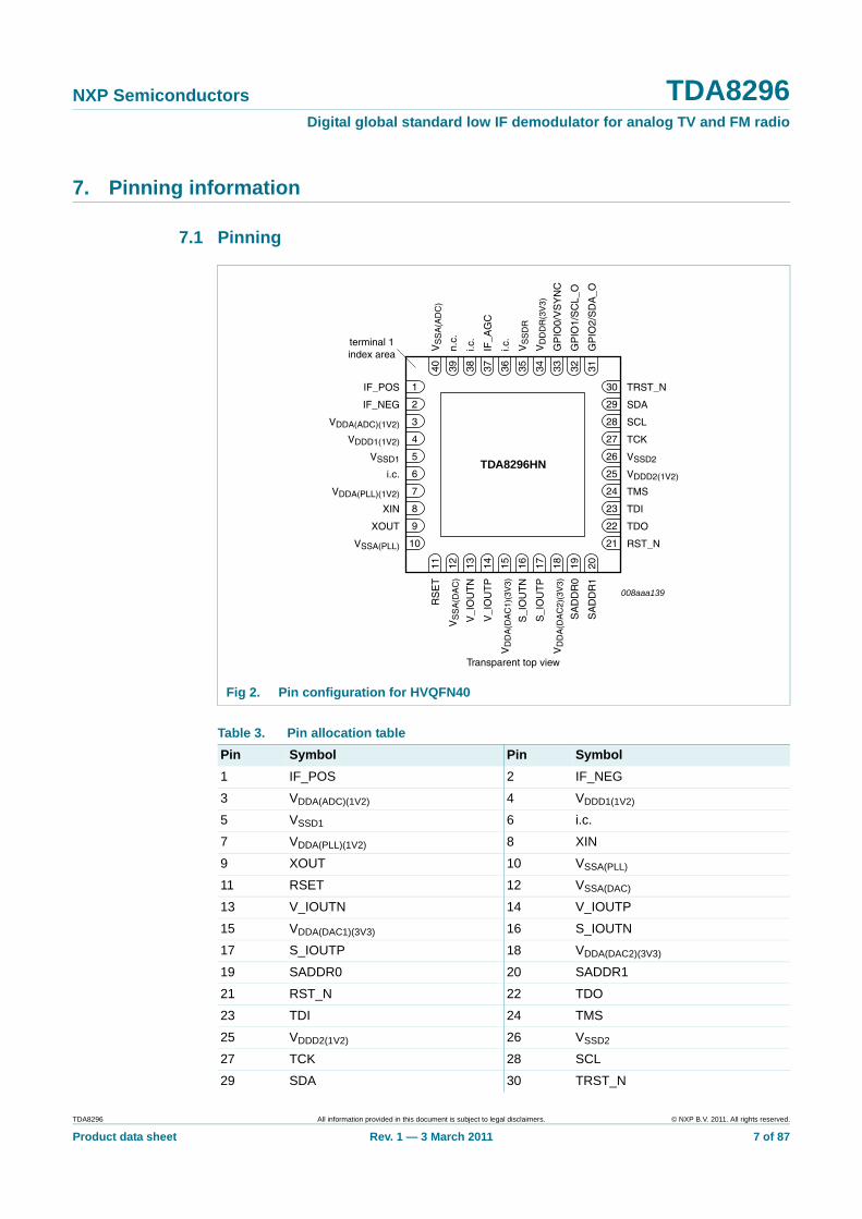
7. Pinning information
7.1 Pinning
Fig 2. Pin configuration for HVQFN40
Table 3. Pin allocation table Pin Symbol Pin Symbol1 IF_POS 2 IF_NEG
3 VDDA(ADC)(1V2) 4 VDDD1(1V2)
5 VSSD1 6 i.c.
7 VDDA(PLL)(1V2) 8 XIN
9 XOUT 10 VSSA(PLL)
11 RSET 12 VSSA(DAC)
13 V_IOUTN 14 V_IOUTP
15 VDDA(DAC1)(3V3) 16 S_IOUTN
17 S_IOUTP 18 VDDA(DAC2)(3V3)
19 SADDR0 20 SADDR1
21 RST_N 22 TDO
23 TDI 24 TMS
25 VDDD2(1V2) 26 VSSD2
27 TCK 28 SCL
29 SDA 30 TRST_N
008aaa139
TDA8296HN
RST_N
XOUT
VSSA(PLL)
TDO
XIN TDI
VDDA(PLL)(1V2) TMS
i.c. VDDD2(1V2)
VSSD1 VSSD2
VDDD1(1V2) TCK
VDDA(ADC)(1V2) SCL
IF_NEG SDA
IF_POS TRST_N
RS
ET
VS
SA
(DA
C)
V_I
OU
TN
V_I
OU
TP
VD
DA
(DA
C1)
(3V
3)
S_I
OU
TN
S_I
OU
TP
VD
DA
(DA
C2)
(3V
3)
SA
DD
R0
SA
DD
R1
VS
SA
(AD
C)
n.c.
i.c.
IF_A
GC
i.c.
VS
SD
R
VD
DD
R(3
V3)
GP
IO0/
VS
YN
C
GP
IO1/
SC
L_O
GP
IO2/
SD
A_O
10 21
9 22
8 23
7 24
6 25
5 26
4 27
3 28
2 29
1 30
11 12 13 14 15 16 17 18 19 20
40 39 38 37 36 35 34 33 32 31
terminal 1index area
Transparent top view
TDA8296 All information provided in this document is subject to legal disclaimers. © NXP B.V. 2011. All rights reserved.
Product data sheet Rev. 1 — 3 March 2011 7 of 87

NXP Semiconductors TDA8296Digital global standard low IF demodulator for analog TV and FM radio
7.2 Pin description
31 GPIO2/SDA_O 32 GPIO1/SCL_O
33 GPIO0/VSYNC 34 VDDDR(3V3)
35 VSSDR 36 i.c.
37 IF_AGC 38 i.c.
39 n.c. 40 VSSA(ADC)
die pad global ground at backside contact
Table 3. Pin allocation table …continued
Pin Symbol Pin Symbol
Table 4. Pin description Symbol Pin Type[1] DescriptionResetRST_N 21 I The RST_N input is asynchronous and active LOW, and clears the TDA8296. When
RST_N goes LOW, the circuit immediately enters its Reset mode and normal operation will resume four XIN signal falling edges later after RST_N returns HIGH. Internal register contents are all initialized to their default values. The minimum width of RST_N at LOW level is four XIN clock periods.
ReferenceXIN 8 I Crystal oscillator input pin. In Slave mode (typically), the XIN input simply receives a
16 MHz clock signal (fREF) from an external device (typically from the TDA1827x). In Oscillator mode, a fundamental 16 MHz (typically) crystal is connected between pin XIN and pin XOUT.
XOUT 9 O Crystal oscillator output pin. In Slave mode, the XOUT output is not connected. In Oscillator mode a fundamental 16 MHz (typically) crystal is connected between pin XIN and pin XOUT.
I2C-busSDA 29 I/O, OD I2C-bus bidirectional serial data. SDA is an open-drain output and therefore requires
an external pull-up resistor (typically 4.7 kΩ).
SCL 28 I I2C-bus clock input. SCL is nominally a square wave with a maximum frequency of 400 kHz. It is generated by the system I2C-bus master.
SADDR0 19 I These two bits allow to select four possible I2C-bus addresses, and therefore permits to use several TDA8296 in the same application and/or to avoid conflict with other ICs. The complete I2C-bus address is: 1, 0, 0, SADDR1, 0, 1, SADDR0, R/W (see also Section 9.1).
SADDR1 20 I
I2C-bus feed-through switch or GPIOGPIO2/SDA_O 31 I/O, OD SDA_O is equivalent to SDA but can be 3-stated by I2C-bus programming. It is the
output of a switch controlled by I2CSW_EN parameter. SDA_O is an open-drain output and therefore requires an external pull-up resistor (see Section 9.3.18).
GPIO1/SCL_O 32 I/O, OD SCL_O is equivalent to SCL input but can be 3-stated by I2C-bus programming. SCL_O is an open-drain output and therefore requires an external pull-up resistor (see Section 9.3.18). For proper functioning of the I2C-bus feed-through, a capacitor C = 33 pF to GND must be added (see Section 13.6).
V-sync or GPIOGPIO0/VSYNC 33 I/O, OD vertical synchronization pulse needed for the NXP Silicon Tuner
(see Section 9.3.18)
Tuner IF AGCIF_AGC 37 I/O, OD, T tuner IF AGC output
TDA8296 All information provided in this document is subject to legal disclaimers. © NXP B.V. 2011. All rights reserved.
Product data sheet Rev. 1 — 3 March 2011 8 of 87

NXP Semiconductors TDA8296Digital global standard low IF demodulator for analog TV and FM radio
[1] The pin types are defined in Table 5.
Boundary scanTMS 24 I Test mode select provides the logic levels needed to change the TAP controller from
state to state during the boundary scan test.
TRST_N 30 I Test reset is used to reset the TAP controller (active LOW). Grounding is mandatory in Functional mode.
TCK 27 I Test clock is used to drive the TAP controller.
TDI 23 I Test data input is the serial data input for the test data instruction.
TDO 22 O Test data output is the serial test data output pin. The data is provided on the falling edge of TCK.
ADCIF_POS 1 AI IF positive analog input for internal ADC
IF_NEG 2 AI IF negative analog input for internal ADC
DACV_IOUTP 14 AO positive analog current output of the video output
V_IOUTN 13 AO negative analog current output of the video output
S_IOUTP 17 AO positive analog current output of the SSIF/mono sound output
S_IOUTN 16 AO negative analog current output of the SSIF/mono sound output
RSET 11 I External bias setting of the DACs. An external resistor (1 kΩ typical) has to be connected between RSET and the analog ground of the board. This resistor generates the current into the DACs and also defines the full scale output current. The total parasitic capacitance seen externally from the RSET pin has to be lower than 20 pF.
Supplies and groundsVDDA(DAC1)(3V3) 15 PS DAC1 (video DAC) and DAC reference module analog supply voltage (3.3 V typical)
VDDA(DAC2)(3V3) 18 PS DAC2 (sound DAC) analog supply voltage (3.3 V typical)
VSSA(DAC) 12 GND DAC reference module analog ground supply voltage (0 V typical)
VDDA(ADC)(1V2) 3 PS IF ADC analog supply voltage (1.2 V typical)
VSSA(ADC) 40 GND ADC analog ground supply voltage (0 V typical)
VDDD1(1V2) 4 PS ADC, PLL and DACs digital supply voltage (1.2 V typical)
VSSD1 5 GND ADC, PLL and DACs digital ground supply voltage (0 V typical)
VDDA(PLL)(1V2) 7 PS crystal oscillator and clock PLL analog supply voltage (1.2 V typical)
VSSA(PLL) 10 GND crystal oscillator and clock PLL analog ground supply voltage (0 V typical)
VDDD2(1V2) 25 PS core digital supply voltage (1.2 V typical)
VSSD2 26 GND core digital ground supply voltage (0 V typical)
VDDDR(3V3) 34 PS ring digital supply voltage (3.3 V typical)
VSSDR 35 GND ring digital ground supply voltage (0 V typical)
VSS die pad GND
Other pinsi.c. 6, 36,
38I internally connected; connect to ground
n.c. 39 I not connected
Table 4. Pin description …continued
Symbol Pin Type[1] Description
TDA8296 All information provided in this document is subject to legal disclaimers. © NXP B.V. 2011. All rights reserved.
Product data sheet Rev. 1 — 3 March 2011 9 of 87
NXP Semiconductors TDA8296Digital global standard low IF demodulator for analog TV and FM radio
8. Functional description
8.1 IF ADCThe low IF spectrum (1 MHz to 10 MHz) from the Silicon Tuner TDA1827x is fed symmetrically to the 12-bit IF ADC of the TDA8296, where it is sampled with 54 MHz or 27 MHz. All the anti-aliasing filtering is already done in the Silicon Tuner.
8.2 FiltersThe internal filters permit to reduce the sampling rate to 13.5 MHz, and to form a complex signal to ease the effort of further signal processing. Before this, the DC offset (coming from the ADC) is removed.
In addition, standard dependent notch filters for the adjacent sound carriers protect the picture carrier PLL from malfunctioning and avoid disturbances (i.e. moire) becoming visible in the video output.
8.3 PLL demodulatorThe second-order PLL is the core block of the whole IC. It is very robust against adverse field conditions, like excessive over modulation, no residual carrier presence or unwanted phase or frequency modulation of the picture carrier. The PLL output is the synchronously demodulated channel.
The AFC data is available via the I2C-bus.
8.4 Nyquist filter, video low-pass filter, video and group delay equalizer, video levelingThe afore-mentioned down-mixed complex signal at the mixer CORDIC output, already consisting of the demodulated content of the picture carrier together with the sound carriers (the so-called intercarriers), is running through a Nyquist filter to get a flat video response and is made real.
Afterwards, a video low-pass filter suppresses the sound carriers and other disturbers.
Next comes the equalizer circuit to remove the transmitter group delay predistortion.
Table 5. Pin type description Type DescriptionAI analog input
AO analog output
GND ground
I digital input
I/O digital input and output
O digital output
OD open-drain output
PS power supply
T 3-state
TDA8296 All information provided in this document is subject to legal disclaimers. © NXP B.V. 2011. All rights reserved.
Product data sheet Rev. 1 — 3 March 2011 10 of 87
NXP Semiconductors TDA8296Digital global standard low IF demodulator for analog TV and FM radio
A video leveling stage follows, which brings the output within the SCART specification (±3 dB overall), despite heavy over modulation. The response time is made very slow.
Finally, a video equalizer allows to compensate the perhaps non-flat frequency response from the tuner or to change the overall video response according to customer wish (i.e. peaking or early roll-off).
8.5 Upsampler and video DACThe filtered and compensated CVBS signal is connected to the oversampled 10-bit video DAC (fs = 108 MHz) via an interpolation stage. The strong oversampling replaces a former complicated LCR postfiltering by a simple first-order RC low-pass filter to remove the DAC image frequencies sufficiently. This holds also for the sound DAC, described in Section 8.6.
8.6 SSIF/mono sound processingThe complex signal is routed via a band-pass, AGC and interpolation filter to the 10-bit sound DAC for the recovery of the second sound carriers (SSIF). A very sharp band-pass filter at 5.5 MHz is added in the FM Radio mode to remove neighbor channels. This also eases the dynamic burden on the following ADC in the demodulator/decoder chip. The afore-mentioned high-selectivity band-pass, which replaces the former ceramic filter, is located behind a frequency shifter. In there, the incoming wanted FM radio channel from the Silicon Tuner is changed from 1.25 MHz to 5.5 MHz.
Moreover, the complex signal is demodulated in a linear CORDIC detector and low-pass filtered to attenuate the video spectrum and the second sound carrier, respectively other disturbers above the intercarrier. The output of the linear CORDIC (phase information) is differentiated for getting the demodulated FM audio. The AM demodulation is executed in a synchronous fashion by using a narrow-band PLL demodulator.
A de-emphasis filter is implemented for FM standards, before the audio is interpolated to 108 MHz as in the CVBS case.
The mono audio is made available in the sound DAC via an I2C-bus controlled selector in case the intercarrier path is not used for driving an external stereo demodulator.
However, if the mono audio output has to meet the SCART specification, an external cheap operational amplifier with 12 dB gain becomes necessary, because the low supply voltage for the TDA8296 doesn’t allow such high levels like 2 V (RMS) maximum.
8.7 Tuner IF AGCThis AGC controls the tuner IF AGC amplifier in the TDA1827x in such a way, that the IF ADC is always running with a permanent headroom of 3 dB for the sum of all signals present at the ADC input. This ensures an always optimal exploitation of the dynamic range in the IF ADC.
The detection is done in peak Search mode during a field period. The attack time is made much faster than the decay time in order to avoid transient clipping effects in the IF ADC. This can happen during channel change or airplane flutter conditions.
TDA8296 All information provided in this document is subject to legal disclaimers. © NXP B.V. 2011. All rights reserved.
Product data sheet Rev. 1 — 3 March 2011 11 of 87

NXP Semiconductors TDA8296Digital global standard low IF demodulator for analog TV and FM radio
The above wideband, slowly acting AGC loop (uncorrelated) is of first-order integral action. It is closed via the continuous tuner IF AGC amplifier in the Silicon Tuner via a bit stream DAC (PWM signal at 13.5 MHz, 27 MHz or 54 MHz) and an external and uncritical first-order RC low-pass.
8.8 Digital IF AGCCommon to both IF AGC concepts is the peak search algorithm as long as the H/V PLL is not locked. This is of advantage for the acquisition by avoiding hang-ups due to excessive overloading, so being able to leave the saturated condition by reducing the gain.
Two Detection modes are made available in the IC via I2C-bus.
• Black level gated AGC:The first mode uses an IF AGC detector which is gated with a very robust and well-proven H/V sync PLL block on board. Gating occurs on the black level (most of the time on the back porch) of the video signal and the control is delivered after an error integration and exponential weighting to the internal IF AGC amplifier. This IF AGC amplifier, in fact a multiplier, has a control range of −20 dB to +48 dB.
• Peak AGC:A fast attack and slow decay action cares for a good and nearly clip-free transient behavior. This proved to be more robust for non-standard signals, like sync clipping along the transmitter/receiver chain.With respect to the IF AGC speed generally, only the gated black level or peak sync digital IF AGC can be made fast. However the peak search tuner IF AGC, used for positive modulation standards (L and L-accent standard), is rather slow because the VITS is present only once in a field.The correlated or narrow-band AGC loop, closed via the continuous IF AGC amplifier in the TDA8296, is of first-order integral action and settles at a constant IF input level with a permanent headroom of 12 dB (picture carrier). This headroom is needed for the own sound carriers and the leaking neighbor (N − 1) spectrum.
8.9 Clock generationFinally, either an external reference frequency (i.e. from the Silicon Tuner) or an own on-chip crystal oscillator in the TDA8296 feeds the internal PLL synthesizer to generate the necessary clock signals.
9. I2C-bus control
9.1 Protocol of the I2C-bus serial interfaceThe TDA8296 internal registers are accessible by means of the I2C-bus serial interface. The SDA bidirectional pin is used as the data input/output pin and SCL as the clock input pin. The highest SCL speed is 400 kHz.
TDA8296 All information provided in this document is subject to legal disclaimers. © NXP B.V. 2011. All rights reserved.
Product data sheet Rev. 1 — 3 March 2011 12 of 87

NXP Semiconductors TDA8296Digital global standard low IF demodulator for analog TV and FM radio
9.1.1 Write mode
Fig 3. I2C-bus Write mode
Table 6. Address format7 6 5 4 3 2 1 01 0 0 SADDR1 0 1 SADDR0 R/W
Table 7. I2C-bus transfer description Field Bit DescriptionS - START condition
Byte 1 7 to 5 device address
4 SADDR1
3 and 2 device address
1 SADDR0
0 R/W = 0 for write action
A - acknowledge
Byte 2 7 to 0 start index
A - acknowledge
Byte 3 7 to 0 data 1
A - acknowledge
:
Byte n 7 to 0 data n
A - acknowledge
P - STOP condition
a. Address 84h, write 02h in register 01h
b. Address 84h, write 05h in register 02h and 04h in register 03h
Fig 4. Examples I2C-bus Write mode
001aad381
BYTE 1 BYTE 2 BYTE 3 BYTE nS A A A A P
address 0 start index data 1 data nstart ack ack ack .... ack stop
001aah355
BYTE 1S A
1000 0100
BYTE 2
0000 0001
BYTE 3
0000 0010start ack
A
ack
A
ack
P
stop
001aah356
BYTE 1S
1000 0100
BYTE 2
0000 0010
BYTE 3
0000 0101
BYTE 4
0000 0100start
A
ack
A
ack
A
ack
A
ack
P
stop
TDA8296 All information provided in this document is subject to legal disclaimers. © NXP B.V. 2011. All rights reserved.
Product data sheet Rev. 1 — 3 March 2011 13 of 87
NXP Semiconductors TDA8296Digital global standard low IF demodulator for analog TV and FM radio
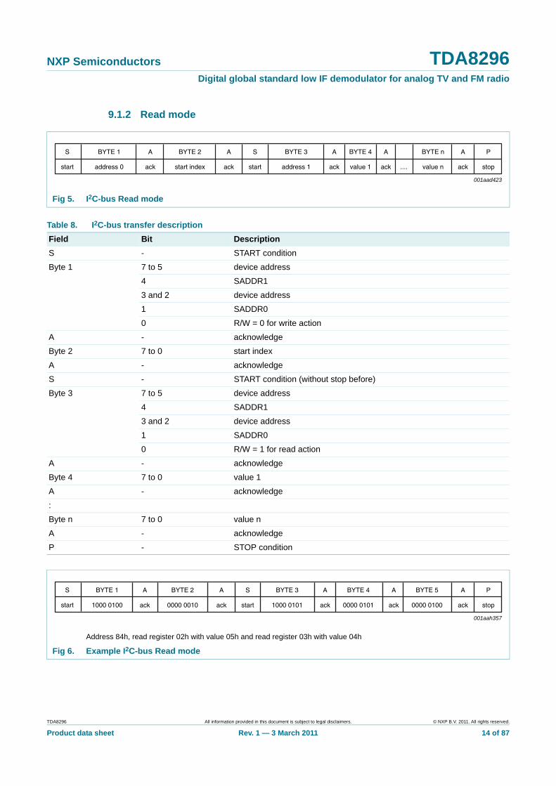
9.1.2 Read mode
Fig 5. I2C-bus Read mode
001aad423
BYTE 1S
address 0
BYTE 2
start index
BYTE 3
address 1
BYTE 4
value 1
BYTE n
value nstart
A
ack
A
ack
A
ack
A
ack ....
A
ack
P
stop
S
start
Table 8. I2C-bus transfer description Field Bit DescriptionS - START condition
Byte 1 7 to 5 device address
4 SADDR1
3 and 2 device address
1 SADDR0
0 R/W = 0 for write action
A - acknowledge
Byte 2 7 to 0 start index
A - acknowledge
S - START condition (without stop before)
Byte 3 7 to 5 device address
4 SADDR1
3 and 2 device address
1 SADDR0
0 R/W = 1 for read action
A - acknowledge
Byte 4 7 to 0 value 1
A - acknowledge
:
Byte n 7 to 0 value n
A - acknowledge
P - STOP condition
Address 84h, read register 02h with value 05h and read register 03h with value 04h
Fig 6. Example I2C-bus Read mode
001aah357
BYTE 1S
1000 0100
BYTE 2
0000 0010
BYTE 3
1000 0101
BYTE 4
0000 0101
BYTE 5
0000 0100start
A
ack
A
ack
A
ack
A
ack
A
ack
P
stop
S
start
TDA8296 All information provided in this document is subject to legal disclaimers. © NXP B.V. 2011. All rights reserved.
Product data sheet Rev. 1 — 3 March 2011 14 of 87

NXP Semiconductors TDA8296Digital global standard low IF demodulator for analog TV and FM radio
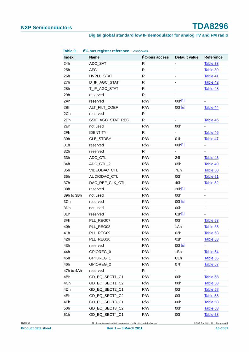
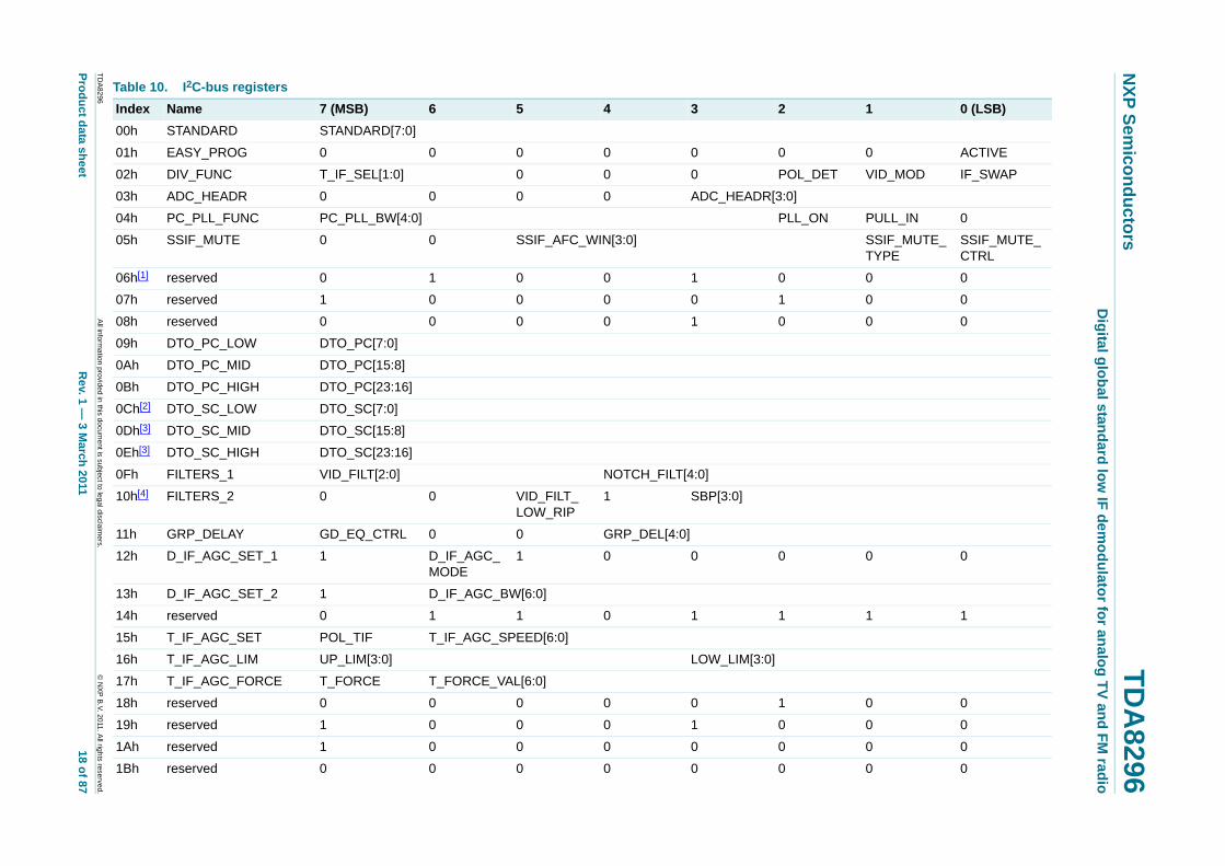
9.2 Register overviewThe TDA8296 internal registers are accessible by means of the I2C-bus serial interface as described in Section 9.1. In Table 10 and Table 9 an overview of all the registers is given, the register description can be found in Section 9.3.
Table 9. I2C-bus register reference Index Name I2C-bus access Default value Reference00h STANDARD R/W 01h Table 11
01h EASY_PROG R/W 00h Table 12
02h DIV_FUNC R/W 04h Table 14
03h ADC_HEADR R/W 01h Table 15
04h PC_PLL_FUNC R/W 24h Table 16
05h SSIF_MUTE R/W 04h Table 33
06h reserved R/W 48h[1] -
07h reserved R/W 84h[1] -
08h reserved R/W 08h[1] -
09h DTO_PC_LOW R/W 9Ah Table 17
0Ah DTO_PC_MID R/W 99h Table 17
0Bh DTO_PC_HIGH R/W 99h Table 17
0Ch DTO_SC_LOW R/W 3Dh Table 19
0Dh DTO_SC_MID R/W 20h Table 19
0Eh DTO_SC_HIGH R/W 59h Table 19
0Fh FILTERS_1 R/W 21h Table 21
10h FILTERS_2 R/W 31h Table 22
11h GRP_DELAY R/W 01h Table 23
12h D_IF_AGC_SET_1 R/W A0h Table 24
13h D_IF_AGC_SET_2 R/W 90h Table 25
14h reserved R/W 67h[1] -
15h T_IF_AGC_SET R/W 88h Table 26
16h T_IF_AGC_LIM R/W F0h Table 27
17h T_IF_AGC_FORCE R/W 3Fh Table 28
18h reserved R/W 02h[1] -
19h reserved R/W 88h[1] -
1Ah reserved R/W 80h[1] -
1Bh reserved R/W 00h[1] -
1Ch V_SYNC_DEL R/W 6Fh Table 29
1Dh CVBS_SET R/W 31h Table 30
1Eh CVBS_LEVEL R/W 73h Table 31
1Fh CVBS_EQ R/W 10h Table 32
20h SOUNDSET_1 R/W 21h Table 34
21h SOUNDSET_2 R/W 22h Table 35
22h SOUND_LEVEL R/W 08h Table 36
23h SSIF_LEVEL R/W AFh Table 37
TDA8296 All information provided in this document is subject to legal disclaimers. © NXP B.V. 2011. All rights reserved.
Product data sheet Rev. 1 — 3 March 2011 15 of 87
NXP Semiconductors TDA8296Digital global standard low IF demodulator for analog TV and FM radio
24h ADC_SAT R - Table 38
25h AFC R - Table 39
26h HVPLL_STAT R - Table 41
27h D_IF_AGC_STAT R - Table 42
28h T_IF_AGC_STAT R - Table 43
29h reserved R - -
2Ah reserved R/W 00h[1] -
2Bh ALT_FILT_COEF R/W 00h[1] Table 44
2Ch reserved R - -
2Dh SSIF_AGC_STAT_REG R - Table 45
2Eh not used R/W 00h -
2Fh IDENTITY R - Table 46
30h CLB_STDBY R/W 01h Table 47
31h reserved R/W 00h[1] -
32h reserved R - -
33h ADC_CTL R/W 24h Table 48
34h ADC_CTL_2 R/W 05h Table 49
35h VIDEODAC_CTL R/W 7Eh Table 50
36h AUDIODAC_CTL R/W 00h Table 51
37h DAC_REF_CLK_CTL R/W 40h Table 52
38h reserved R/W 20h[1] -
39h to 3Bh not used R/W 00h -
3Ch reserved R/W 00h[1] -
3Dh not used R/W 00h -
3Eh reserved R/W 61h[1] -
3Fh PLL_REG07 R/W 00h Table 53
40h PLL_REG08 R/W 1Ah Table 53
41h PLL_REG09 R/W 02h Table 53
42h PLL_REG10 R/W 01h Table 53
43h reserved R/W 00h[1] -
44h GPIOREG_0 R/W 1Bh Table 54
45h GPIOREG_1 R/W C1h Table 55
46h GPIOREG_2 R/W 07h Table 57
47h to 4Ah reserved R - -
4Bh GD_EQ_SECT1_C1 R/W 00h Table 58
4Ch GD_EQ_SECT1_C2 R/W 00h Table 58
4Dh GD_EQ_SECT2_C1 R/W 00h Table 58
4Eh GD_EQ_SECT2_C2 R/W 00h Table 58
4Fh GD_EQ_SECT3_C1 R/W 00h Table 58
50h GD_EQ_SECT3_C2 R/W 00h Table 58
51h GD_EQ_SECT4_C1 R/W 00h Table 58
Table 9. I2C-bus register reference …continued
Index Name I2C-bus access Default value Reference
TDA8296 All information provided in this document is subject to legal disclaimers. © NXP B.V. 2011. All rights reserved.
Product data sheet Rev. 1 — 3 March 2011 16 of 87

NXP Semiconductors TDA8296Digital global standard low IF demodulator for analog TV and FM radio
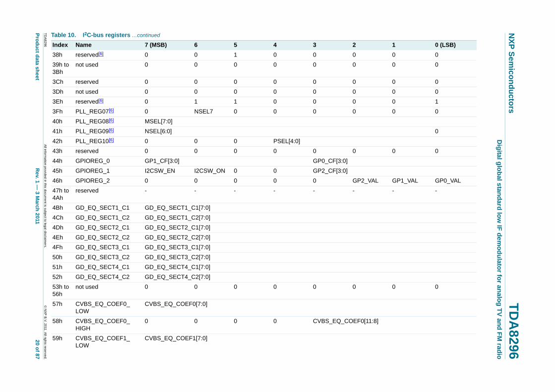
[1] This register must not be written with values other than default.
52h GD_EQ_SECT4_C2 R/W 00h Table 58
53h to 56h not used R/W 00h -
57h CVBS_EQ_COEF0_LOW R/W 00h Table 60
58h CVBS_EQ_COEF0_HIGH R/W 00h Table 60
59h CVBS_EQ_COEF1_LOW R/W 00h Table 60
5Ah CVBS_EQ_COEF1_HIGH R/W 00h Table 60
5Bh CVBS_EQ_COEF2_LOW R/W 00h Table 60
5Ch CVBS_EQ_COEF2_HIGH R/W 00h Table 60
5Dh CVBS_EQ_COEF3_LOW R/W 00h Table 60
5Eh CVBS_EQ_COEF3_HIGH R/W 00h Table 60
5Fh CVBS_EQ_COEF4_LOW R/W 00h Table 60
60h CVBS_EQ_COEF4_HIGH R/W 00h Table 60
61h CVBS_EQ_COEF5_LOW R/W 00h Table 60
62h CVBS_EQ_COEF5_HIGH R/W 04h Table 60
63h to 66h not used R/W 00h -
67h reserved R/W FEh[1] -
68h reserved R/W 0Fh[1] -
69h reserved R/W FAh[1] -
6Ah reserved R/W 0Fh[1] -
6Bh reserved R/W EFh[1] -
6Ch reserved R/W 0Fh[1] -
6Dh reserved R/W DDh[1] -
6Eh reserved R/W 0Fh[1] -
6Fh reserved R/W BEh[1] -
70h reserved R/W 0Fh[1] -
71h reserved R/W 8Ah[1] -
72h reserved R/W 0Fh[1] -
73h reserved R/W 32h[1] -
74h reserved R/W 0Fh[1] -
75h reserved R/W 6Fh[1] -
76h reserved R/W 0Eh[1] -
77h reserved R/W F4h[1] -
78h reserved R/W 0Ah[1] -
79h to 7Bh not used R/W 00h -
7Ch to 9Ch reserved R/W 00h[1] -
9Dh to A0h not used R/W 00h -
A1h and A2h reserved R/W 00h[1] -
Table 9. I2C-bus register reference …continued
Index Name I2C-bus access Default value Reference
TDA8296 All information provided in this document is subject to legal disclaimers. © NXP B.V. 2011. All rights reserved.
Product data sheet Rev. 1 — 3 March 2011 17 of 87
xxxxxxxxxxxxxxxxxxxxx xxxxxxxxxxxxxxxxxxxxxxxxxx xxxxxxx x x x xxxxxxxxxxxxxxxxxxxxxxxxxxxxxx xxxxxxxxxxxxxxxxxxx xx xx xxxxx xxxxxxxxxxxxxxxxxxxxxxxxxxx xxxxxxxxxxxxxxxxxxx xxxxxx xxxxxxxxxxxxxxxxxxxxxxxxxxxxxxxxxxx xxxxxxxxxxxx x x xxxxxxxxxxxxxxxxxxxxx xxxxxxxxxxxxxxxxxxxxxxxxxxxxxx xxxxx xxxxxxxxxxxxxxxxxxxxxxxxxxxxxxxxxxxxxxxxxxxxxxxxxx xxxxxxxx xxxxxxxxxxxxxxxxxxxxxxxxx xxxxxxxxxxxxxxxxxxxx xxx
TDA8296
Product data sh
NXP Sem
iconductorsTD
A8296
Digital global standard low
IF demodulator for analog TV and FM
radio
Table 10. I2C-bus registers Index Name 7 (MSB) 6 5 4 3 2 1 0 (LSB)00h STANDARD STANDARD[7:0]
01h EASY_PROG 0 0 0 0 0 0 0 ACTIVE
DET VID_MOD IF_SWAP
ON PULL_IN 0
SSIF_MUTE_ TYPE
SSIF_MUTE_ CTRL
0 0
0 0
0 0
0 0
1 1
0 0
0 0
0 0
0 0
All information provided in this docum
ent is subject to legal disclaimers.
© N
XP B
.V. 2011. All rights reserved.
eetR
ev. 1 — 3 M
arch 2011 18 of 87
02h DIV_FUNC T_IF_SEL[1:0] 0 0 0 POL_
03h ADC_HEADR 0 0 0 0 ADC_HEADR[3:0]
04h PC_PLL_FUNC PC_PLL_BW[4:0] PLL_
05h SSIF_MUTE 0 0 SSIF_AFC_WIN[3:0]
06h[1] reserved 0 1 0 0 1 0
07h reserved 1 0 0 0 0 1
08h reserved 0 0 0 0 1 0
09h DTO_PC_LOW DTO_PC[7:0]
0Ah DTO_PC_MID DTO_PC[15:8]
0Bh DTO_PC_HIGH DTO_PC[23:16]
0Ch[2] DTO_SC_LOW DTO_SC[7:0]
0Dh[3] DTO_SC_MID DTO_SC[15:8]
0Eh[3] DTO_SC_HIGH DTO_SC[23:16]
0Fh FILTERS_1 VID_FILT[2:0] NOTCH_FILT[4:0]
10h[4] FILTERS_2 0 0 VID_FILT_ LOW_RIP
1 SBP[3:0]
11h GRP_DELAY GD_EQ_CTRL 0 0 GRP_DEL[4:0]
12h D_IF_AGC_SET_1 1 D_IF_AGC_MODE
1 0 0 0
13h D_IF_AGC_SET_2 1 D_IF_AGC_BW[6:0]
14h reserved 0 1 1 0 1 1
15h T_IF_AGC_SET POL_TIF T_IF_AGC_SPEED[6:0]
16h T_IF_AGC_LIM UP_LIM[3:0] LOW_LIM[3:0]
17h T_IF_AGC_FORCE T_FORCE T_FORCE_VAL[6:0]
18h reserved 0 0 0 0 0 1
19h reserved 1 0 0 0 1 0
1Ah reserved 1 0 0 0 0 0
1Bh reserved 0 0 0 0 0 0

xxxxxxxxxxxxxxxxxxxxx xxxxxxxxxxxxxxxxxxxxxxxxxx xxxxxxx x x x xxxxxxxxxxxxxxxxxxxxxxxxxxxxxx xxxxxxxxxxxxxxxxxxx xx xx xxxxx xxxxxxxxxxxxxxxxxxxxxxxxxxx xxxxxxxxxxxxxxxxxxx xxxxxx xxxxxxxxxxxxxxxxxxxxxxxxxxxxxxxxxxx xxxxxxxxxxxx x x xxxxxxxxxxxxxxxxxxxxx xxxxxxxxxxxxxxxxxxxxxxxxxxxxxx xxxxx xxxxxxxxxxxxxxxxxxxxxxxxxxxxxxxxxxxxxxxxxxxxxxxxxx xxxxxxxx xxxxxxxxxxxxxxxxxxxxxxxxx xxxxxxxxxxxxxxxxxxxx xxx
TDA8296
Product data sh
NXP Sem
iconductorsTD
A8296
Digital global standard low
IF demodulator for analog TV and FM
radio1Ch V_SYNC_DEL VS_WIDTH[1:0] VS_POL VS_DEL[4:0]
1Dh CVBS_SET 0 0 1[5] 1 CVBS_EQ_ FOR_BLK AUTO_BLK 1
_ SSIF_SND[1:0]
CK F_H_LOCK N_H_LOCK
- -
0 0
ALT_FILT_COEF[1:0]
- -
0 0
STDBY CLB
0 0
- -
SLEEP PD_ADC
0 AD_SR54M
PD_DA_V
PD_DA_S
0 PD_DA_REF
Table 10. I2C-bus registers …continued
Index Name 7 (MSB) 6 5 4 3 2 1 0 (LSB)
All information provided in this docum
ent is subject to legal disclaimers.
© N
XP B
.V. 2011. All rights reserved.
eetR
ev. 1 — 3 M
arch 2011 19 of 87
CTRL
1Eh CVBS_LEVEL CVBS_LVL[7:0]
1Fh CVBS_EQ CVBS_EQ[7:0]
20h SOUNDSET_1 0 AM_FM_SND[1:0] DEEMPH[4:0]
21h SOUNDSET_2 0 SSIF_AGC_TC
SSIF_AGC_ CTRL
HD_DK FOR_MUTE AUTOMUTE
22h SOUND_LEVEL 0 0 0 SND_LVL[4:0]
23h SSIF_LEVEL SSIF_LVL[7:0]
24h ADC_SAT ADC_SAT[7:0]
25h AFC AFC[7:0]
26h HVPLL_STAT - - NOISE_DET MAC_DET FIDT V_LO
27h D_IF_AGC_STAT D_IF_AGC_STAT[7:0]
28h T_IF_AGC_STAT T_IF_AGC_STAT[7:0]
29h reserved - - - - - -
2Ah reserved 0 0 0 0 0 0
2Bh ALT_FILT_COEF[6] 0 0 0 0 0 0
2Ch reserved - - - - - -
2Dh SSIF_AGC_STAT SSIF_AGC_STAT[7:0]
2Eh not used 0 0 0 0 0 0
2Fh IDENTITY IDENTITY[7:0]
30h CLB_STDBY 0 0 0 0 0 0
31h reserved 0 0 0 0 0 0
32h reserved - - - - - -
33h ADC_CTL 0 0 1 0 DCIN 1
34h ADC_CTL_2 0 0 0 0 0 1
35h VIDEODAC_CTL 0 B_DA_V[5:0]
36h AUDIODAC_CTL 0 B_DA_S[5:0]
37h DAC_REF_CLK_CTL 0 1 0 0 0 0
xxxxxxxxxxxxxxxxxxxxx xxxxxxxxxxxxxxxxxxxxxxxxxx xxxxxxx x x x xxxxxxxxxxxxxxxxxxxxxxxxxxxxxx xxxxxxxxxxxxxxxxxxx xx xx xxxxx xxxxxxxxxxxxxxxxxxxxxxxxxxx xxxxxxxxxxxxxxxxxxx xxxxxx xxxxxxxxxxxxxxxxxxxxxxxxxxxxxxxxxxx xxxxxxxxxxxx x x xxxxxxxxxxxxxxxxxxxxx xxxxxxxxxxxxxxxxxxxxxxxxxxxxxx xxxxx xxxxxxxxxxxxxxxxxxxxxxxxxxxxxxxxxxxxxxxxxxxxxxxxxx xxxxxxxx xxxxxxxxxxxxxxxxxxxxxxxxx xxxxxxxxxxxxxxxxxxxx xxx
TDA8296
Product data sh
NXP Sem
iconductorsTD
A8296
Digital global standard low
IF demodulator for analog TV and FM
radio38h reserved[6] 0 0 1 0 0 0 0 0
39h to not used 0 0 0 0 0 0 0 0
0 0
0 0
0 1
0 0
0
0 0
VAL GP1_VAL GP0_VAL
- -
0 0
11:8]
Table 10. I2C-bus registers …continued
Index Name 7 (MSB) 6 5 4 3 2 1 0 (LSB)
All information provided in this docum
ent is subject to legal disclaimers.
© N
XP B
.V. 2011. All rights reserved.
eetR
ev. 1 — 3 M
arch 2011 20 of 87
3Bh
3Ch reserved 0 0 0 0 0 0
3Dh not used 0 0 0 0 0 0
3Eh reserved[6] 0 1 1 0 0 0
3Fh PLL_REG07[6] 0 NSEL7 0 0 0 0
40h PLL_REG08[6] MSEL[7:0]
41h PLL_REG09[6] NSEL[6:0]
42h PLL_REG10[6] 0 0 0 PSEL[4:0]
43h reserved 0 0 0 0 0 0
44h GPIOREG_0 GP1_CF[3:0] GP0_CF[3:0]
45h GPIOREG_1 I2CSW_EN I2CSW_ON 0 0 GP2_CF[3:0]
46h GPIOREG_2 0 0 0 0 0 GP2_
47h to 4Ah
reserved - - - - - -
4Bh GD_EQ_SECT1_C1 GD_EQ_SECT1_C1[7:0]
4Ch GD_EQ_SECT1_C2 GD_EQ_SECT1_C2[7:0]
4Dh GD_EQ_SECT2_C1 GD_EQ_SECT2_C1[7:0]
4Eh GD_EQ_SECT2_C2 GD_EQ_SECT2_C2[7:0]
4Fh GD_EQ_SECT3_C1 GD_EQ_SECT3_C1[7:0]
50h GD_EQ_SECT3_C2 GD_EQ_SECT3_C2[7:0]
51h GD_EQ_SECT4_C1 GD_EQ_SECT4_C1[7:0]
52h GD_EQ_SECT4_C2 GD_EQ_SECT4_C2[7:0]
53h to 56h
not used 0 0 0 0 0 0
57h CVBS_EQ_COEF0_ LOW
CVBS_EQ_COEF0[7:0]
58h CVBS_EQ_COEF0_ HIGH
0 0 0 0 CVBS_EQ_COEF0[
59h CVBS_EQ_COEF1_ LOW
CVBS_EQ_COEF1[7:0]

xxxxxxxxxxxxxxxxxxxxx xxxxxxxxxxxxxxxxxxxxxxxxxx xxxxxxx x x x xxxxxxxxxxxxxxxxxxxxxxxxxxxxxx xxxxxxxxxxxxxxxxxxx xx xx xxxxx xxxxxxxxxxxxxxxxxxxxxxxxxxx xxxxxxxxxxxxxxxxxxx xxxxxx xxxxxxxxxxxxxxxxxxxxxxxxxxxxxxxxxxx xxxxxxxxxxxx x x xxxxxxxxxxxxxxxxxxxxx xxxxxxxxxxxxxxxxxxxxxxxxxxxxxx xxxxx xxxxxxxxxxxxxxxxxxxxxxxxxxxxxxxxxxxxxxxxxxxxxxxxxx xxxxxxxx xxxxxxxxxxxxxxxxxxxxxxxxx xxxxxxxxxxxxxxxxxxxx xxx
TDA8296
Product data sh
NXP Sem
iconductorsTD
A8296
Digital global standard low
IF demodulator for analog TV and FM
radio5Ah CVBS_EQ_COEF1_
HIGH0 0 0 0 CVBS_EQ_COEF1[11:8]
11:8]
11:8]
11:8]
11:8]
0 0
1 0
1 1
1 0
1 1
1 1
1 1
0 1
1 1
1 0
1 1
1 0
1 1
1 0
Table 10. I2C-bus registers …continued
Index Name 7 (MSB) 6 5 4 3 2 1 0 (LSB)
All information provided in this docum
ent is subject to legal disclaimers.
© N
XP B
.V. 2011. All rights reserved.
eetR
ev. 1 — 3 M
arch 2011 21 of 87
5Bh CVBS_EQ_COEF2_ LOW
CVBS_EQ_COEF2[7:0]
5Ch CVBS_EQ_COEF2_ HIGH
0 0 0 0 CVBS_EQ_COEF2[
5Dh CVBS_EQ_COEF3_ LOW
CVBS_EQ_COEF3[7:0]
5Eh CVBS_EQ_COEF3_ HIGH
0 0 0 0 CVBS_EQ_COEF3[
5Fh CVBS_EQ_COEF4_ LOW
CVBS_EQ_COEF4[7:0]
60h CVBS_EQ_COEF4_ HIGH
0 0 0 0 CVBS_EQ_COEF4[
61h CVBS_EQ_COEF5_ LOW
CVBS_EQ_COEF5[7:0]
62h CVBS_EQ_COEF5_ HIGH
0 0 0 0 CVBS_EQ_COEF5[
63h to 66h
not used 0 0 0 0 0 0
67h reserved 1 1 1 1 1 1
68h reserved 0 0 0 0 1 1
69h reserved 1 1 1 1 1 0
6Ah reserved 0 0 0 0 1 1
6Bh reserved 1 1 1 0 1 1
6Ch reserved 0 0 0 0 1 1
6Dh reserved 1 1 0 1 1 1
6Eh reserved 0 0 0 0 1 1
6Fh reserved 1 0 1 1 1 1
70h reserved 0 0 0 0 1 1
71h reserved 1 0 0 0 1 0
72h reserved 0 0 0 0 1 1
73h reserved 0 0 1 1 0 0

xxxxxxxxxxxxxxxxxxxxx xxxxxxxxxxxxxxxxxxxxxxxxxx xxxxxxx x x x xxxxxxxxxxxxxxxxxxxxxxxxxxxxxx xxxxxxxxxxxxxxxxxxx xx xx xxxxx xxxxxxxxxxxxxxxxxxxxxxxxxxx xxxxxxxxxxxxxxxxxxx xxxxxx xxxxxxxxxxxxxxxxxxxxxxxxxxxxxxxxxxx xxxxxxxxxxxx x x xxxxxxxxxxxxxxxxxxxxx xxxxxxxxxxxxxxxxxxxxxxxxxxxxxx xxxxx xxxxxxxxxxxxxxxxxxxxxxxxxxxxxxxxxxxxxxxxxxxxxxxxxx xxxxxxxx xxxxxxxxxxxxxxxxxxxxxxxxx xxxxxxxxxxxxxxxxxxxx xxx
TDA8296
Product data sh
NXP Sem
iconductorsTD
A8296
Digital global standard low
IF demodulator for analog TV and FM
radio
sample frequency.
74h reserved 0 0 0 0 1 1 1 1
75h reserved 0 1 1 0 1 1 1 1
1 0
0 0
1 0
0 0
0 0
0 0
0 0
Table 10. I2C-bus registers …continued
Index Name 7 (MSB) 6 5 4 3 2 1 0 (LSB)
All information provided in this docum
ent is subject to legal disclaimers.
© N
XP B
.V. 2011. All rights reserved.
eetR
ev. 1 — 3 M
arch 2011 22 of 87
[1] Register 06h has to be reprogrammed to new value C4h.
[2] Register 0Ch has to be reprogrammed to new value 00h.
[3] For M/N standard (ADC clock at 54 MHz) register 0Dh and 0Eh have to be reprogrammed to new value 55h.
[4] For M/N standard use narrow SSIF band-pass filter (SBP[3:0] = 0100).
[5] For L/L-accent standard the bit has to be programmed to 0.
[6] These registers have to be programmed to the alternative value in Table 66, if an other frequency is required than 54 MHz for ADC
76h reserved 0 0 0 0 1 1
77h reserved 1 1 1 1 0 1
78h reserved 0 0 0 0 1 0
79h to 7Bh
not used 0 0 0 0 0 0
7Ch to 9Ch
reserved 0 0 0 0 0 0
9Dh to A0h
not used 0 0 0 0 0 0
A1h and A2h
reserved 0 0 0 0 0 0

NXP Semiconductors TDA8296Digital global standard low IF demodulator for analog TV and FM radio
9.3 Register descriptionIf registers (or bit groups contained in registers) are programmed with invalid values, i.e. values different from those described in the tables below, the default behavior is chosen for the related block. Other settings than described in the tables are not allowed.
9.3.1 Standard setting with easy programmingWith the implemented ‘easy programming’, only one bit sets the TV or FM radio standard with recommended register content. If not suitable however, any of these registers can be written with other settings. With the rising edge of the bit ACTIVE, some of the registers 02h to 23h are programmed internally with the standard dependent settings according to Table 13. The content of registers with address 24h and higher is untouched.
In addition to application specific software settings following general recommendation should be used (deviating from easy programming values):
• Register 06h: new value C4h• Register 0Ch: new value 00h• M/N standard:
– Register 10h: use narrow SSIF band-pass filter (SBP[3:0] = 0100)– Register 0Dh and 0Eh: new value 55h
Remark: When using alternative ADC sampling frequencies the DTO settings have to be adapted accordingly.
Table 11. STANDARD register (address 00h) bit description Legend: * = default value.
Bit Symbol Access Value Description7 to 0 STANDARD[7:0
]R/W TV or FM radio standard selection (easy
programming)
0000 0001* M/N standard
0000 0010 B standard
0000 0100 G/H standard
0000 1000 I standard
0001 0000 D/K standard
0010 0000 L standard
0100 0000 L-accent standard
1000 0000 FM radio
Table 12. EASY_PROG register (address 01h) bit description Legend: * = default value.
Bit Symbol Access Value Description7 to 1 - R/W 000 0000* not used
0 ACTIVE R/W With the rising edge of this bit, the registers 02h to 23h are programmed with the standard dependent settings (see Table 13).
0* no action
1 no action
0 to 1 activate easy programming
TDA8296 All information provided in this document is subject to legal disclaimers. © NXP B.V. 2011. All rights reserved.
Product data sheet Rev. 1 — 3 March 2011 23 of 87
NXP Semiconductors TDA8296Digital global standard low IF demodulator for analog TV and FM radio
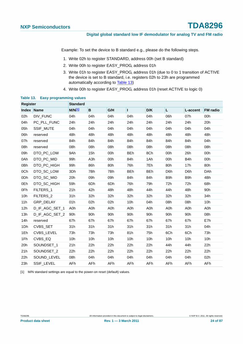
Example: To set the device to B standard e.g., please do the following steps.
1. Write 02h to register STANDARD, address 00h (set B standard)2. Write 00h to register EASY_PROG, address 01h3. Write 01h to register EASY_PROG, address 01h (due to 0 to 1 transition of ACTIVE
the device is set to B standard, i.e. registers 02h to 23h are programmed automatically according to Table 13)
4. Write 00h to register EASY_PROG, address 01h (reset ACTIVE to logic 0)
[1] M/N standard settings are equal to the power-on reset (default) values.
Table 13. Easy programming values Register StandardIndex Name M/N[1] B G/H I D/K L L-accent FM radio02h DIV_FUNC 04h 04h 04h 04h 04h 06h 07h 00h
04h PC_PLL_FUNC 24h 24h 24h 24h 24h 24h 24h 20h
05h SSIF_MUTE 04h 04h 04h 04h 04h 04h 04h 04h
06h reserved 48h 48h 48h 48h 48h 48h 48h 48h
07h reserved 84h 84h 84h 84h 84h 84h 84h 04h
08h reserved 08h 08h 08h 08h 08h 08h 08h 08h
09h DTO_PC_LOW 9Ah 15h 00h BEh 8Ch 00h 26h 00h
0Ah DTO_PC_MID 99h A3h 00h 84h 1Ah 00h B4h 00h
0Bh DTO_PC_HIGH 99h 86h 80h 76h 7Eh 80h 17h 80h
0Ch DTO_SC_LOW 3Dh 7Bh 7Bh BEh BEh D6h D6h DAh
0Dh DTO_SC_MID 20h 09h 09h 84h 84h B9h B9h 4Bh
0Eh DTO_SC_HIGH 59h 6Dh 6Dh 76h 79h 72h 72h 68h
0Fh FILTERS_1 21h 42h 48h 48h 44h 44h 48h 90h
10h FILTERS_2 31h 32h 32h 32h 32h 32h 32h 34h
11h GRP_DELAY 01h 02h 02h 10h 04h 08h 08h 10h
12h D_IF_AGC_SET_1 A0h A0h A0h A0h A0h A0h A0h A0h
13h D_IF_AGC_SET_2 90h 90h 90h 90h 90h 90h 90h 08h
14h reserved 67h 67h 67h 67h 67h 67h 67h E7h
1Dh CVBS_SET 31h 31h 31h 31h 31h 31h 31h 04h
1Eh CVBS_LEVEL 73h 73h 73h 81h 75h 6Ch 6Ch 73h
1Fh CVBS_EQ 10h 10h 10h 10h 10h 10h 10h 10h
20h SOUNDSET_1 21h 22h 22h 22h 22h 44h 44h 22h
21h SOUNDSET_2 22h 22h 22h 22h 22h 22h 22h 22h
22h SOUND_LEVEL 08h 04h 04h 04h 04h 04h 04h 02h
23h SSIF_LEVEL AFh AFh AFh AFh AFh AFh AFh AFh
TDA8296 All information provided in this document is subject to legal disclaimers. © NXP B.V. 2011. All rights reserved.
Product data sheet Rev. 1 — 3 March 2011 24 of 87
NXP Semiconductors TDA8296Digital global standard low IF demodulator for analog TV and FM radio
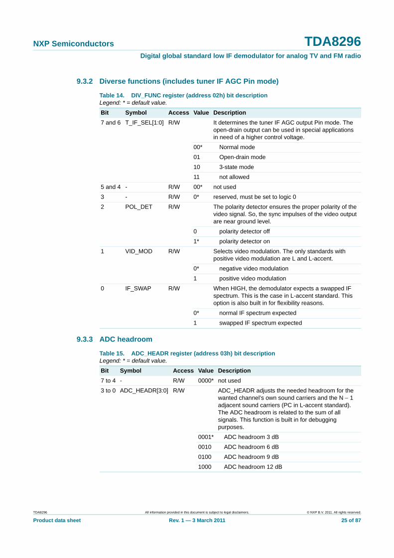
9.3.2 Diverse functions (includes tuner IF AGC Pin mode)
9.3.3 ADC headroom
Table 14. DIV_FUNC register (address 02h) bit description Legend: * = default value.
Bit Symbol Access Value Description7 and 6 T_IF_SEL[1:0] R/W It determines the tuner IF AGC output Pin mode. The
open-drain output can be used in special applications in need of a higher control voltage.
00* Normal mode
01 Open-drain mode
10 3-state mode
11 not allowed
5 and 4 - R/W 00* not used
3 - R/W 0* reserved, must be set to logic 0
2 POL_DET R/W The polarity detector ensures the proper polarity of the video signal. So, the sync impulses of the video output are near ground level.
0 polarity detector off
1* polarity detector on
1 VID_MOD R/W Selects video modulation. The only standards with positive video modulation are L and L-accent.
0* negative video modulation
1 positive video modulation
0 IF_SWAP R/W When HIGH, the demodulator expects a swapped IF spectrum. This is the case in L-accent standard. This option is also built in for flexibility reasons.
0* normal IF spectrum expected
1 swapped IF spectrum expected
Table 15. ADC_HEADR register (address 03h) bit description Legend: * = default value.
Bit Symbol Access Value Description7 to 4 - R/W 0000* not used
3 to 0 ADC_HEADR[3:0] R/W ADC_HEADR adjusts the needed headroom for the wanted channel’s own sound carriers and the N − 1 adjacent sound carriers (PC in L-accent standard). The ADC headroom is related to the sum of all signals. This function is built in for debugging purposes.
0001* ADC headroom 3 dB
0010 ADC headroom 6 dB
0100 ADC headroom 9 dB
1000 ADC headroom 12 dB
TDA8296 All information provided in this document is subject to legal disclaimers. © NXP B.V. 2011. All rights reserved.
Product data sheet Rev. 1 — 3 March 2011 25 of 87
NXP Semiconductors TDA8296Digital global standard low IF demodulator for analog TV and FM radio
9.3.4 Picture carrier PLL functions
[1] The DTO_PC frequency is set via register 09h to 0Bh
[2] The DTO_PC frequency is controlled by VIF_PLL function
9.3.5 Picture and sound carrier DTO
Table 16. PC_PLL_FUNC register (address 04h) bit description Legend: * = default value.
Bit Symbol Access Value Description7 to 3 PC_PLL_BW[4:0] R/W picture carrier PLL loop bandwidth selection
0 0001 loop bandwidth 15 kHz (not recommanded)
0 0010 loop bandwidth 30 kHz
0 0100* loop bandwidth 60 kHz
0 1000 loop bandwidth 130 kHz
1 0000 loop bandwidth 280 kHz (not recommanded)
2 PLL_ON R/W the picture carrier PLL can be disengaged (e.g. in FM radio standard)
0 PLL off (FM radio)[1]
1* PLL on[2]
1 PULL_IN R/W PULL_IN selects the pull-in range of the picture carrier PLL/FPLL
0* pull-in range ±1.66 MHz
1 pull-in range ±830 kHz
0 - R/W 0* reserved, must be set to logic 0
Table 17. DTO_PC_LOW, DTO_PC_MID and DTO_PC_HIGH register (address 09h to 0Bh) bit description Legend: * = default value.
Address Register Bit Symbol Access Value Description09h DTO_PC_LOW 7 to 0 DTO_PC[7:0] R/W 9Ah* For picture processing the digital tuned oscillator
(DTO_PC) provides its oscillation signal to the demodulator part. For demodulation the oscillation frequency of the DTO_PC is controlled by the VIF_PLL. Optional the DTO_PC can operate at fixed programmed frequency. This will be the case if PLL_ON register is set to “off” mode. In case of VIF_PLL mode of the DTO_PC the register value defines the nominal frequency of AFC register (seeTable 39). If PLL_ON register is set to “off” mode the DTO_PC register defines the fixed oscillation frequency value of the DTO_PC. The frequency of the DTO_PC is in relation to the register value by following formula:
.
In case of standard L’ please use the following
formula:
0Ah DTO_PC_MID 7 to 0 DTO_PC[15:8] R/W 99h*
0Bh DTO_PC_HIGH 7 to 0 DTO_PC[23:16] R/W 99h*
DTO_PCfADC 4⁄ fPC–
fADC 4⁄--------------------------------- 224×=
DTO_PC fPC4
fADC-----------× 224×=
TDA8296 All information provided in this document is subject to legal disclaimers. © NXP B.V. 2011. All rights reserved.
Product data sheet Rev. 1 — 3 March 2011 26 of 87
NXP Semiconductors TDA8296Digital global standard low IF demodulator for analog TV and FM radio
[1] Deviating from easy programming values for DTO_SC[23:0] the values from Table 20 should be used.
(1) relation for L’(2) relation for systems L; M/N; B/G; I; D/K
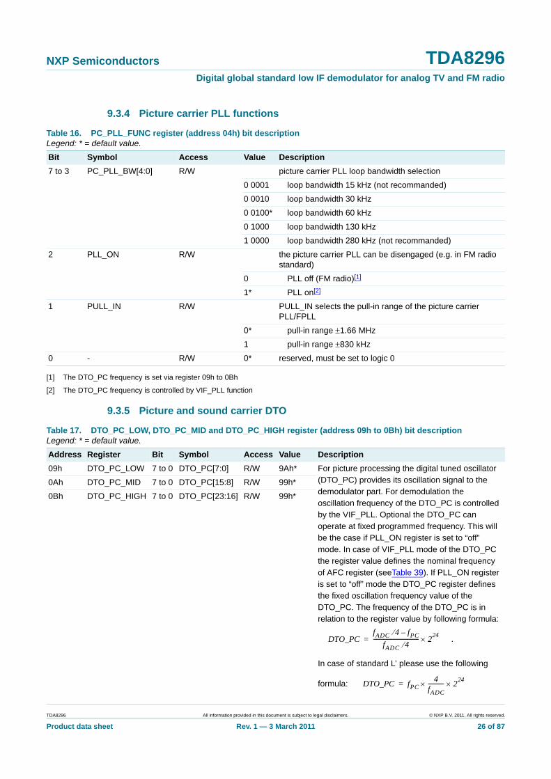
Fig 7. TDA8296 DTO_PC characteristic
DTO_PC reg val (dec) (1E6)0 1284
001aan388
4
6
2
8
10DTO_PCfrequency
value(MHz)
0
(1)
(2)
Table 18. Values of DTO_PC per TV standard at 54 MHz sampling frequencyStandard DTO_SC[23:16] DTO_SC[15:8] DTO_SC[7:0] DTO_PC frequency valueM/N 99h 99h 9Ah 5.40 MHz
B 86h A3h 15h 6.40 MHz
G 80h 00h 00h 6.75 MHz
I 76h 84h BEh 7.25 MHz
D/K 7Eh 1Ah 8Ch 6.85 MHz
L 80h 00h 00h 6.75 MHz
L-accent 17h B4h 26h 1.25 MHz
Table 19. DTO_SC_LOW, DTO_SC_MID and DTO_SC_HIGH register (address 0Ch to 0Eh) bit description Legend: * = default value.[1]
Address Register Bit Symbol Access Value Description0Ch DTO_SC_LOW 7 to 0 DTO_SC[7:0] R/W 00h* The DTO_SC is suited for SSIF band-pass filter
tuning. DTO_SC is calculated according to the following formula, whereas fSC is the SSIF band-pass center frequency:
.
0Dh DTO_SC_MID 7 to 0 DTO_SC[15:8] R/W 20h*
0Eh DTO_SC_HIGH 7 to 0 DTO_SC[23:16] R/W 59h*
DTO_SCfSC
fADC 4⁄------------------ 224×=
TDA8296 All information provided in this document is subject to legal disclaimers. © NXP B.V. 2011. All rights reserved.
Product data sheet Rev. 1 — 3 March 2011 27 of 87

NXP Semiconductors TDA8296Digital global standard low IF demodulator for analog TV and FM radio
9.3.6 Filter settings
Fig 8. TDA8296 DTO_SC characteristic
DTO reg val (dec) (1E6)0 1284
001aam354
4
6
2
8
10
Fsc[MHz]
0
Table 20. Values for SSIF mode at 54 MHz sampling frequency Standard DTO_SC[23:16] DTO_SC[15:8] DTO_SC[7:0] Band-pass center frequencyM/N 55h 55h 00h 4.5 MHz
B 6Dh 09h 00h 5.75 MHz
G/H 6Dh 09h 00h 5.75 MHz
I 76h 84h 00h 6.25 MHz
D/K 76h 84h 00h 6.25 MHz
L/L-accent 72h B9h 00h 6.05 MHz
FM radio 68h 4Bh 00h 5.5 MHz
Table 21. FILTERS_1 register (address 0Fh) bit description Legend: * = default value.
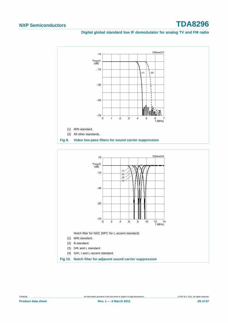
Bit Symbol Access Value Description7 to 5 VID_FILT[2:0] R/W video low-pass filter to remove all unwanted frequencies
(own sound carriers) above video content (see Figure 9)
001* video low-pass filter 4 MHz
010 video low-pass filter 5 MHz
100 video low-pass filter off
4 to 0 NOTCH_FILT[4:0] R/W The notch filter attenuates the adjacent sound carrier N − 1, which is located differently dependent on standard (see Figure 10).
0 0001* notch filter at 6.9 MHz for M/N standard
0 0010 notch filter at 7.9 MHz for B standard
0 0100 notch filter at 8.3 MHz for D/K and L standard
0 1000 notch filter at 9.25 MHz for G/H, I and L-accent standard
1 0000 notch filter bypass
TDA8296 All information provided in this document is subject to legal disclaimers. © NXP B.V. 2011. All rights reserved.
Product data sheet Rev. 1 — 3 March 2011 28 of 87
NXP Semiconductors TDA8296Digital global standard low IF demodulator for analog TV and FM radio
(1) M/N standard.(2) All other standards.
Fig 9. Video low-pass filters for sound carrier suppression
Notch filter for NSC (NPC for L-accent standard)(1) M/N standard.(2) B standard.(3) D/K and L standard.(4) G/H, I and L-accent standard.
Fig 10. Notch filter for adjacent sound carrier suppression
f (MHz)0 762 4 51 3
008aaa223
−30
−50
−10
10
αresp(f)(dB)
−70
(1) (2)
f (MHz)0 14124 8 102 6
008aaa224
−30
−50
−10
10
αresp(f)(dB)
−70
(1)(2)(3)(4)
TDA8296 All information provided in this document is subject to legal disclaimers. © NXP B.V. 2011. All rights reserved.
Product data sheet Rev. 1 — 3 March 2011 29 of 87
NXP Semiconductors TDA8296Digital global standard low IF demodulator for analog TV and FM radio
[1] SSIF band-pass center frequency is controlled by DTO_SC[23:0]. See Table 20 for recommended DTO values.
[2] Deviating from easy programming values for FILTERS_2, the narrow SSIF band-pass filter (SPB[3:0] = 0100) should be used for M/N standard.
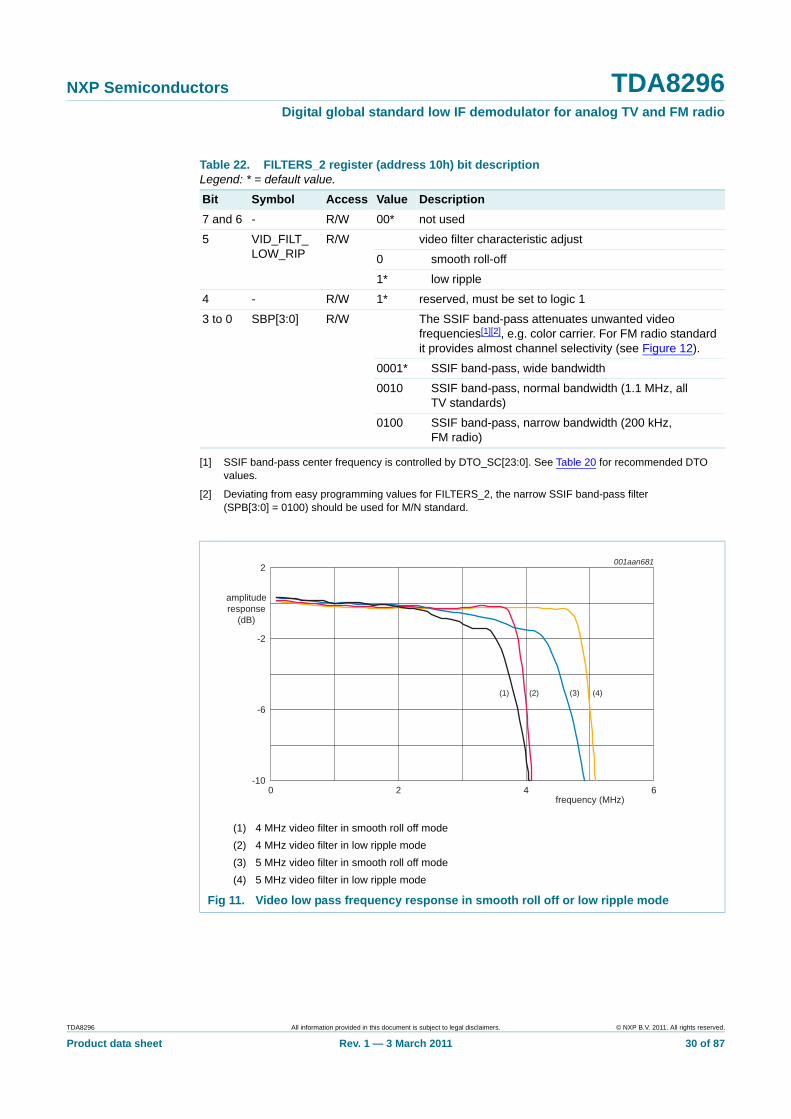
Table 22. FILTERS_2 register (address 10h) bit description Legend: * = default value.
Bit Symbol Access Value Description7 and 6 - R/W 00* not used
5 VID_FILT_ LOW_RIP
R/W video filter characteristic adjust
0 smooth roll-off
1* low ripple
4 - R/W 1* reserved, must be set to logic 1
3 to 0 SBP[3:0] R/W The SSIF band-pass attenuates unwanted video frequencies[1][2], e.g. color carrier. For FM radio standard it provides almost channel selectivity (see Figure 12).
0001* SSIF band-pass, wide bandwidth
0010 SSIF band-pass, normal bandwidth (1.1 MHz, all TV standards)
0100 SSIF band-pass, narrow bandwidth (200 kHz, FM radio)
(1) 4 MHz video filter in smooth roll off mode(2) 4 MHz video filter in low ripple mode(3) 5 MHz video filter in smooth roll off mode(4) 5 MHz video filter in low ripple mode
Fig 11. Video low pass frequency response in smooth roll off or low ripple mode
frequency (MHz)0 62
-6
-2
2
amplituderesponse
(dB)
-10
(1) (2) (3) (4)
4
001aan681
TDA8296 All information provided in this document is subject to legal disclaimers. © NXP B.V. 2011. All rights reserved.
Product data sheet Rev. 1 — 3 March 2011 30 of 87

NXP Semiconductors TDA8296Digital global standard low IF demodulator for analog TV and FM radio
9.3.7 Group delay equalization
(1) Wide bandwidth (e.g. for search mode).(2) All TV standards, normal bandwidth (1.1 MHz).(3) FM radio, narrow bandwidth (200 kHz).
Fig 12. SSIF and FM radio band-pass filters (center frequency 5.5 MHz chosen)
f (MHz)0 14124 8 102 6
008aaa228
−30
−50
−10
10
αresp(f)(dB)
−70
(1)(2)(3)
Table 23. GRP_DELAY register (address 11h) bit description Legend: * = default value.
Bit Symbol Access Value Description7 GD_EQ_CTRL R/W group delay equalizer control; this is the control for
the freely programmable group delay equalizer; for details see Section 9.3.19
0* off (equalizer bypassed)
1 on (equalizer active)
6 and 5 - R/W 00* reserved, must be set to logic 00
4 to 0 GRP_DEL[4:0] R/W group delay equalization to correct the transmitter predistortion
0 0001* group delay M/N standard
0 0010 group delay B/G/H standard
0 0100 group delay D/K standard
0 1000 group delay L/L-accent standard
1 0000 group delay I (flat) standard
TDA8296 All information provided in this document is subject to legal disclaimers. © NXP B.V. 2011. All rights reserved.
Product data sheet Rev. 1 — 3 March 2011 31 of 87

NXP Semiconductors TDA8296Digital global standard low IF demodulator for analog TV and FM radio
9.3.8 Digital IF AGC functions
9.3.9 Tuner IF AGC functions
Table 24. D_IF_AGC_SET_1 register (address 12h) bit description Legend: * = default value.
Bit Symbol Access Value Description7 - R/W 1* reserved, must be set to logic 1
6 D_IF_AGC_MODE R/W If HIGH, the digital IF AGC detection and gating is done during the back porch of the video signal. This Detection mode can be used for all standards (also L/L-accent standard) without impact on the IF AGC loop speed.
0* peak sync AGC (slow peak white L/L-accent standard)
1 black level AGC detection
5 to 0 - R/W 10 0000* reserved, must be set to logic 10 0000
Table 25. D_IF_AGC_SET_2 register (address 13h) bit description Legend: * = default value.
Bit Symbol Access Value Description7 - R/W 1* reserved, must be set to logic 1
6 to 0 D_IF_AGC_BW[6:0] R/W digital IF AGC 3 dB-loop bandwidth setting
000 0001 25 Hz
000 0010 50 Hz
000 0100 100 Hz
000 1000 200 Hz
001 0000* 400 Hz
010 0000 800 Hz
100 0000 1.6 kHz (not recommended)
Table 26. T_IF_AGC_SET register (address 15h) bit description Legend: * = default value.
Bit Symbol Access Value Description7 POL_TIF R/W tuner IF AGC polarity
0 inverted tuner IF AGC polarity
1* normal tuner IF AGC polarity: the higher the necessary gain, the higher the IF AGC voltage
TDA8296 All information provided in this document is subject to legal disclaimers. © NXP B.V. 2011. All rights reserved.
Product data sheet Rev. 1 — 3 March 2011 32 of 87
NXP Semiconductors TDA8296Digital global standard low IF demodulator for analog TV and FM radio
6 to 0 T_IF_AGC_SPEED[6:0] R/W T_IF_AGC_SPEED determines the tuner IF AGC loop speed
000 0001 −18 dB nominal
000 0010 −12 dB nominal
000 0100 −6 dB nominal
000 1000* nominal speed (determined by the tuner IF control slope)
001 0000 +6 dB nominal
010 0000 +12 dB nominal
100 0000 +18 dB nominal
Table 27. T_IF_AGC_LIM register (address 16h) bit description Legend: * = default value.
Bit Symbol Access Value Description7 to 4 UP_LIM[3:0] R/W The tuner IF AGC output voltage can be limited to
interface with concepts having power supply < 3.3 V. UP_LIM determines the upper limit from 1∨2 FS (= 0h) to FS (= Fh). The format is straight binary.
1111* set upper limit to maximum
3 to 0 LOW_LIM[3:0] R/W LOW_LIM determines the lower tuner IF AGC output limit from 0 (= 0h) to 1∨2 FS (= Fh). The format is straight binary.
0000* set lower limit to minimum
Table 28. T_IF_AGC_FORCE register (address 17h) bit description Legend: * = default value.
Bit Symbol Access Value Description7 T_FORCE R/W the tuner IF AGC output voltage can be forced
externally to a fixed voltage, determined by T_FORCE_VAL
0* tuner IF AGC normal operation
1 tuner IF AGC output voltage determined by T_FORCE_VAL
6 to 0 T_FORCE_VAL[6:0] R/W T_FORCE_VAL determines the tuner IF AGC forced value. So the tuner IF AGC can be fixed to a certain value for debugging purposes. Format is straight binary.
3Fh* 0.5 × VDD(3V3), i.e. 1.65 V nominally
XXh don’t care if T_FORCE = 0
Table 26. T_IF_AGC_SET register (address 15h) bit description …continuedLegend: * = default value.
Bit Symbol Access Value Description
TDA8296 All information provided in this document is subject to legal disclaimers. © NXP B.V. 2011. All rights reserved.
Product data sheet Rev. 1 — 3 March 2011 33 of 87
NXP Semiconductors TDA8296Digital global standard low IF demodulator for analog TV and FM radio
9.3.10 V-sync adjustment
9.3.11 CVBS settings
Table 29. V_SYNC_DEL register (address 1Ch) bit description Legend: * = default value.
Bit Symbol Access Value Description7 and 6 VS_WIDTH[1:0] R/W VS_WIDTH determines the width (in horizontal
lines) of the V-sync gating pulse (needed for gating of tuner RF AGC2)
00 width 1 line (64 μs)
01* width 2 lines
10 width 4 lines
11 width 16 lines
5 VS_POL R/W VS_POL determines the polarity of the V-sync pulse: if VS_POL = 1, the first edge of the pulse is positive, else negative.
0 first edge negative
1* first edge positive
4 to 0 VS_DEL[4:0] R/W VS_DEL determines the first edge position of the output V-sync pulse compared to the beginning of the vertical blanking interval:
0Fh* first edge 3 lines after beginning of vertical interval
pulse_position VS_DEL 12–( ) lines=
Table 30. CVBS_SET register (address 1Dh) bit description Legend: * = default value.
Bit Symbol Access Value Description7 and 6 - R/W 00* not used
5 and 4 - R/W 11* must be set to logic 11 or in case of L/L-accent to 01
3 CVBS_EQ_CTRL
R/W video equalizer mode control
0* mode using predefined settings like described in Table 32
1 free programmable mode; for details see Section 9.3.19
2 FOR_BLK R/W when active, the video output is always blanked, e.g. for channel change (forced blank)
0* no action
1 video blanked
1 AUTO_BLK R/W when active, the video output is blanked if the horizontal line lock flag (N_H_LOCK, see Table 41) is not present
0* auto-blanking off
1 auto-blanking on
0 - R/W 1* reserved, must be set to logic 1
TDA8296 All information provided in this document is subject to legal disclaimers. © NXP B.V. 2011. All rights reserved.
Product data sheet Rev. 1 — 3 March 2011 34 of 87
NXP Semiconductors TDA8296Digital global standard low IF demodulator for analog TV and FM radio
Table 31. CVBS_LEVEL register (address 1Eh) bit description Legend: * = default value.
Bit Symbol Access Value Description7 to 0 CVBS_LVL[7:0] R/W With this byte, the nominal video output level is freely
programmable. The format is unsigned integer (offset binary). Settings below 40h and above C0h, which correspond to −5 dB (40h) and +4.5 dB (C0h) related to the default value, are forbidden. In the following some possible settings in 1 dB steps are shown.
51h −3 dB nominal
5Bh −2 dB nominal
66h −1 dB nominal
73h* nominal: 1 V (p-p) video output level (sync-peak)
81h +1 dB nominal
91h +2 dB nominal
A2h +3 dB nominal
Table 32. CVBS_EQ register (address 1Fh) bit description Legend: * = default value.
Bit Symbol Access Value Description7 to 0 CVBS_EQ[7:0] R/W The video equalizer can be used for the
compensation of a principal tuner tilt or to change the video frequency according to customer taste. The figures given are at 5 MHz CVBS with respect to low frequencies (see Figure 13).
0000 0001 The video frequency response is −8 dB for 5 MHz.
0000 0010 The video frequency response is −6 dB for 5 MHz.
0000 0100 The video frequency response is −4 dB for 5 MHz.
0000 1000 The video frequency response is −2 dB for 5 MHz.
0001 0000* The video frequency response is made flat in this mode.
0010 0000 The video frequency response is +2 dB (peaking) for 5 MHz.
0100 0000 The video frequency response is +4 dB (peaking) for 5 MHz.
1000 0000 The video frequency response is +6 dB (peaking) for 5 MHz.
TDA8296 All information provided in this document is subject to legal disclaimers. © NXP B.V. 2011. All rights reserved.
Product data sheet Rev. 1 — 3 March 2011 35 of 87

NXP Semiconductors TDA8296Digital global standard low IF demodulator for analog TV and FM radio
9.3.12 SSIF and mono sound settings
Fig 13. Video equalizer curves
f (MHz)0 762 41 3 5
001aah361
−2
2
−6
6
10
αresp(f)(dB)
−10
Table 33. SSIF_MUTE register (address 05h) bit description Legend: * = default value.
Bit Symbol Access Value Description7 and 6 - R/W 00* not used
5 to 2 SSIF_AFC_WIN[3:0] R/W SSIF AFC mute window configuration
0001* ±100 kHz
0010 ±200 kHz
0100 ±400 kHz
1000 ±800 kHz
1 SSIF_MUTE_TYPE R/W SSIF auto-mute behavior
0* reduced gain
1 mute
0 SSIF_MUTE_CTRL R/W auto-mute of SSIF output
0* off
1 on
Table 34. SOUNDSET_1 register (address 20h) bit description Legend: * = default value.
Bit Symbol Access Value Description7 - R/W 0* reserved, must be set to logic 0
6 and 5 AM_FM_SND[1:0] R/W Output mode for inbuilt FM/AM mono sound demodulator
01* FM sound
10 AM sound (only L/L-accent standard)
XX don’t care if SSIF output is chosen (SSIF_SND[1:0] = 10)
TDA8296 All information provided in this document is subject to legal disclaimers. © NXP B.V. 2011. All rights reserved.
Product data sheet Rev. 1 — 3 March 2011 36 of 87

NXP Semiconductors TDA8296Digital global standard low IF demodulator for analog TV and FM radio
4 to 0 DEEMPH[4:0] R/W mono sound de-emphasis adjustment to compensate transmitter pre-emphasis; or low-pass filter to remove out of audio band interferers
0 0001* de-emphasis of 75 μs for M/N standard or non-European FM radio to compensate the transmitter pre-emphasis
0 0010 de-emphasis of 50 μs for B/G/H, D/K and I standard or European FM radio to compensate the transmitter pre-emphasis
0 0100 low-pass filter with 30 kHz −3 dB cut-off frequency to remove out of audio band interferers
0 1000 low-pass filter with 140 kHz −3 dB cut-off frequency to drive an external BTSC stereo decoder
1 0000 The de-emphasis filter is bypassed. This can be used for debugging or other purposes.
Table 34. SOUNDSET_1 register (address 20h) bit description …continuedLegend: * = default value.
Bit Symbol Access Value Description
Table 35. SOUNDSET_2 register (address 21h) bit description Legend: * = default value.
Bit Symbol Access Value Description7 - R/W 0* reserved, must be set to logic 0
6 SSIF_AGC_TC R/W SSIF AGC time constant for L/L-accent standard
0* slow (normal)
1 fast
5 SSIF_AGC_CTRL R/W SSIF AGC control
0 SSIF AGC off
1* SSIF AGC on
4 HD_DK R/W When active, the internal FM mono sound demodulator can handle excessive FM deviations up to 400 kHz. This might happen in D/K standard China. To activate this mode, it is mandatory to set D/K standard first. The sound output level has to be adapted accordingly by the microprocessor to avoid sound DAC clipping. E.g. for 400 kHz FM deviation, the −12 dB setting of the sound level register (see Table 36) is recommended.
0* high Deviation mode off
1 high Deviation mode on
X don’t care if SSIF output is chosen (SSIF_SND[1:0] = 10)
3 FOR_MUTE R/W When active, the mono sound signal is always muted. This setting only makes sense in case the sound DAC output is also set to mono sound (SSIF_SND[1:0] = 01). FOR_MUTE has no function if SSIF_SND[1:0] = 10.
0* off
1 on
X don’t care if SSIF output is chosen (SSIF_SND[1:0] = 10)
TDA8296 All information provided in this document is subject to legal disclaimers. © NXP B.V. 2011. All rights reserved.
Product data sheet Rev. 1 — 3 March 2011 37 of 87

NXP Semiconductors TDA8296Digital global standard low IF demodulator for analog TV and FM radio
[1] Before activating mono sound, the TV standard needs to be set via easy programming
2 AUTO_MUTE R/W When active, the mono sound signal is muted if the horizontal lock flag (N_H_LOCK) disappears. This setting only makes sense in case the sound DAC output is also set to mono sound (SSIF_SND[1:0] = 01). FOR_MUTE has no function if SSIF_SND[1:0] =10.
0* off
1 on
X don’t care if SSIF output is chosen (SSIF_SND[1:0] = 10)
1 and 0 SSIF_SND[1:0] R/W either mono sound or SSIF can be chosen for the sound DAC output
01 mono sound[1]
10* SSIF
Table 35. SOUNDSET_2 register (address 21h) bit description …continuedLegend: * = default value.
Bit Symbol Access Value Description
Table 36. SOUND_LEVEL register (address 22h) bit description Legend: * = default value.
Bit Symbol Access Value Description7 to 5 - R/W 000* not used
4 to 0 SND_LVL[4:0] R/W mono sound output level
0 0001 −12 dB nominal; implemented for flexibility reasons. With this setting, the adaptation to different standard requirements can be done.
0 0010 −6 dB nominal; implemented for flexibility reasons. With this setting, the adaptation to different standard requirements can be done. It is chosen for FM radio because of the large FM deviation involved.
0 0100 Nominal setting; FM deviations up to 100 kHz can be processed without sound DAC clipping. The clipping level is 535 mV (RMS) typically.
0 1000* +6 dB nominal; chosen for M/N standard due to less nominal frequency deviation
1 0000 +12 dB nominal; implemented for flexibility reasons. With this setting, the adaptation to different standard requirements can be done.
X XXXX don’t care if SSIF output is chosen (SSIF_SND[1:0] = 10)
TDA8296 All information provided in this document is subject to legal disclaimers. © NXP B.V. 2011. All rights reserved.
Product data sheet Rev. 1 — 3 March 2011 38 of 87
NXP Semiconductors TDA8296Digital global standard low IF demodulator for analog TV and FM radio
Remark: The SSIF level depends also on the used capacitor CS. Please refer to Figure 14
Table 37. SSIF_LEVEL register (address 23h) bit description Legend: * = default value.
Bit Symbol Access Value Description7 to 0 SSIF_LVL[7:0] R/W SSIF output level adjustment; SSIF AGC on
(21h[5] = 1)
1111 1111 +3 dB
: :
1010 1111* 0 dB
: :
0100 0000 to 0000 0000
−8.7 dB
SSIF output level adjustment; SSIF AGC off (21h[5] = 0)
XXX0 0001 −12 dB nominal; implemented for flexibility reasons. With this setting, the adaptation to different standard requirements can be done.
XXX0 0010 −6 dB nominal; implemented for flexibility reasons. With this setting, the adaptation to different standard requirements can be done.
XXX0 0100 Nominal setting; typical output level is 55 mV (RMS) for PC / SC ratio of 13 dB (see Section 12, SSIF/mono sound output).
XXX0 1000 +6 dB nominal; implemented for flexibility reasons. With this setting, the adaptation to different standard requirements can be done.
XXX1 0000 +12 dB nominal; implemented for flexibility reasons. With this setting, the adaptation to different standard requirements can be done.
XXXX XXXX don’t care if mono sound output is chosen (SSIF_SND[1:0] = 01)
TDA8296 All information provided in this document is subject to legal disclaimers. © NXP B.V. 2011. All rights reserved.
Product data sheet Rev. 1 — 3 March 2011 39 of 87
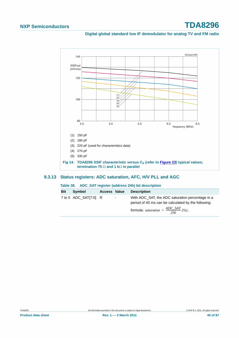
NXP Semiconductors TDA8296Digital global standard low IF demodulator for analog TV and FM radio
9.3.13 Status registers: ADC saturation, AFC, H/V PLL and AGC
(1) 150 pF(2) 180 pF(3) 220 pF (used for characteristics data)(4) 270 pF(5) 330 pF
Fig 14. TDA8296 SSIF characteristic versus CS (refer to Figure 23) typical values; termination 75 Ω and 1 kΩ in parallel
frequency (MHz)4.5 6.56.05.55.0
001aam355
100
120
140
SSIFout(mVrms)
80
(1)(2)(3)(4)(5)
Table 38. ADC_SAT register (address 24h) bit description Bit Symbol Access Value Description7 to 0 ADC_SAT[7:0] R - With ADC_SAT, the ADC saturation percentage in a
period of 40 ms can be calculated by the following
formula: .saturation ADC_SAT256
------------------------- (%)=
TDA8296 All information provided in this document is subject to legal disclaimers. © NXP B.V. 2011. All rights reserved.
Product data sheet Rev. 1 — 3 March 2011 40 of 87

NXP Semiconductors TDA8296Digital global standard low IF demodulator for analog TV and FM radio
[1] See Section 12 for nominal IF frequencies.
Table 39. AFC register (address 25h) bit description Bit Symbol Access Value Description7 to 0 AFC[7:0] R - This is the readout for AFC. AFC contains the
frequency deviation from nominal IF picture carrier. The format is twos complement, 13.2 kHz steps are done per LSB. See Table 40 for details. The frequency deviation could also be given by the following formula:
. For a frequency
deviation from the nominal IF picture carrier greater than the FPLL pull-in capability (−830.6 kHz to +843.8 kHz or −1 674.3 kHz to +1 687.5 kHz), the output reading is undefined. The AFC lock indication can be taken from the N_H_LOCK information from the H-sync PLL. The lock occurs inside a frequency window, which is determined by the pull-in capability of the FPLL.
Table 40. Calculation of frequency deviation from AFC valueDeviation from nominal IF frequency[1]
AFC[7] AFC[6] AFC[5] AFC[4] AFC[3] AFC[2] AFC[1] AFC[0]
fIF = fnom − 1 674.3 kHz 0 1 1 1 1 1 1 1
fIF = fnom − 1 661.1 kHz 0 1 1 1 1 1 1 0
: : : : : : : : :
fIF = fnom − 830.6 kHz 0 0 1 1 1 1 1 1
fIF = fnom − 817.4 kHz 0 0 1 1 1 1 1 0
: : : : : : : : :
fIF = fnom − 13.2 kHz 0 0 0 0 0 0 0 1
fIF = fnom 0 0 0 0 0 0 0 0
fIF = fnom + 13.2 kHz 1 1 1 1 1 1 1 1
: : : : : : : : :
fIF = fnom + 830.6 kHz 1 1 0 0 0 0 0 1
fIF = fnom + 843.8 kHz 1 1 0 0 0 0 0 0
: : : : : : : : :
fIF = fnom + 1 674.3 kHz 1 0 0 0 0 0 0 1
fIF = fnom + 1 687.5 kHz 1 0 0 0 0 0 0 0
fIF fnom– AFC– 6 750×512
---------------------------------- (kHz)=
TDA8296 All information provided in this document is subject to legal disclaimers. © NXP B.V. 2011. All rights reserved.
Product data sheet Rev. 1 — 3 March 2011 41 of 87

NXP Semiconductors TDA8296Digital global standard low IF demodulator for analog TV and FM radio
(1) Undefined area in 1660 kHz mode(2) Undefined area in 830 kHz mode
Fig 15. TDA8296 AFC characteristic
Table 41. HVPLL_STAT register (address 26h) bit description Bit Symbol Access Value Description7 and 6 - R - not used
5 NOISE_DET R - This flag gets HIGH in case the video S/N (weighted) drops below 30 dB. For proper and noise free video signals it stays LOW. It can be used for debugging and other purposes.
4 MAC_DET R - This flag indicates the presence of copy-guarded video content from STBs or VCRs. It can be used for debugging and other purposes.
3 FIDT R - This flag indicates the frame rate (50 Hz or 60 Hz). When active, 60 Hz is detected. It can be used for debugging and other purposes.
2 V_LOCK R - This flag is active, if a proper frame (50 Hz or 60 Hz) is detected. It can be used for debugging and other purposes.
1 F_H_LOCK R - This flag is active, if a proper H-sync (15.625 kHz or 15.734 kHz) is detected (Fast mode). It can be used for debugging and other purposes.
0 N_H_LOCK R - This flag is active, if a proper H-sync (15.625 kHz or 15.734 kHz) is detected (Normal mode). It can be used for debugging and other purposes.
001aam356
Df (MHz)−2000 200010000−1000
−50
50
150
AFCreg val
−150
(1) (1)(2) (2)±830 kHz PLL lock mode
±1660 kHz PLL lock mode
TDA8296 All information provided in this document is subject to legal disclaimers. © NXP B.V. 2011. All rights reserved.
Product data sheet Rev. 1 — 3 March 2011 42 of 87
NXP Semiconductors TDA8296Digital global standard low IF demodulator for analog TV and FM radio
9.3.14 Chip identification and Standby mode
Table 42. D_IF_AGC_STAT register (address 27h) bit description Bit Symbol Access Value Description7 to 0 D_IF_AGC_STAT[7:0] R - D_IF_AGC_STAT is the digital IF AGC status
readout byte. Contains the digital IF AGC loop DC information. The format is twos complement. To get the internal gain in dB, the following formula can be used:
.
Table 43. T_IF_AGC_STAT register (address 28h) bit description Bit Symbol Access Value Description7 to 0 T_IF_AGC_STAT[7:0] R - T_IF_AGC_STAT is the IF AGC status readout
byte. Contains the tuner IF AGC loop DC information. The format is offset binary.
Table 44. ALT_FILT_COEF register (address 2Bh) bit description Bit Symbol Access Value Description Frequency7 to 2 not used R/W 0 not used.
1 to 0 ALT_FILT_COEF R/W 00 internal selection of fixed coefficients for video low pass filter using an ADC sampling frequency of
54.00 MHz
01 50.75 MHz
10 57.25 MHz
Table 45. SSIF_AGC_STAT register (address 2Dh) bit description Bit Symbol Access Value Description7 to 0 SSIF_AGC_STAT[7:0] R - SSIF_AGC_STAT contains the SSIF AGC gain
information. To get the internal gain in dB, the following formula can be used:
. The value is
approximately the PC / SC ratio.
gain D_IF_AGC_STAT 50+3.675
-------------------------------------------------------- (dB)=
gain 20 SSIF_AGC_STAT8
-------------------------------------------10
log=
Table 46. IDENTITY register (address 2Fh) bit description Bit Symbol Access Value Description7 to 0 IDENTITY[7:0] R 1000 1100* chip identification, value corresponds to TDA8296
Table 47. CLB_STDBY register (address 30h) bit description Legend: * = default value.
Bit Symbol Access Value Description7 to 3 - R/W 0000 0* not used
2 - R/W 0* reserved, must be set to logic 0
TDA8296 All information provided in this document is subject to legal disclaimers. © NXP B.V. 2011. All rights reserved.
Product data sheet Rev. 1 — 3 March 2011 43 of 87

NXP Semiconductors TDA8296Digital global standard low IF demodulator for analog TV and FM radio
9.3.15 ADC controlIn the TDA8296 a 12-bit ADC is implemented sampling with a 54 MHz clock (27 MHz optional).
1 STDBY R/W When STDBY is set to logic 1, the chip enters in Standby mode, and its power consumption is reduced. The IF AGC pin is set to high-ohmic. The default value is logic 0, which means that the chip is active.
0* Normal mode
1 Standby mode
0 CLB R/W This signal clears the TDA8296 through the I2C-bus interface (software reset). To activate the reset, just write CLB = 0. This software reset will not affect the content of the registers.
0 activate soft reset
1* normal operation
Table 47. CLB_STDBY register (address 30h) bit description …continuedLegend: * = default value.
Bit Symbol Access Value Description
Table 48. ADC_CTL register (address 33h) bit description Legend: * = default value.
Bit Symbol Access Value Description7 to 4 - R/W 0010* reserved, must be set to logic 0010
3 DCIN R/W The input signal of the ADC can be either AC coupled by means of two capacitors or connected directly to the inputs (DC coupled).
0* AC coupling
1 DC coupling
2 - R/W 1* reserved, must be set to logic 1
1 SLEEP R/W When HIGH, SLEEP sets the ADC into its Sleep mode. Both bias current and clock are switched off. In this mode, the current consumption is reduced by a factor of 6. The reference circuit will remain active in order to guarantee a fast recovery from Sleep mode.
0* Normal mode
1 ADC Sleep mode
0 PD_ADC R/W When HIGH, PD_ADC sets the ADC into its Power-down mode. All internal currents are switched off. In this mode, the current consumption is near zero (leakage current only).
0* Normal mode
1 ADC Power-down mode
Table 49. ADC_CTL_2 register (address 34h) bit description Legend: * = default value.
Bit Symbol Access Value Description7 to 3 - R/W 0000 0* not used
2 and 1 - R/W 10* reserved, must be set to logic 10
TDA8296 All information provided in this document is subject to legal disclaimers. © NXP B.V. 2011. All rights reserved.
Product data sheet Rev. 1 — 3 March 2011 44 of 87

NXP Semiconductors TDA8296Digital global standard low IF demodulator for analog TV and FM radio
9.3.16 Video and sound DAC controlThe TDA8296 implements two 10-bit DAC modules (CVBS and sound outputs) which are sampled by a 108 MHz clock. A reference module derives biasing currents for the two DACs.
0 AD_SR54M R/W AD_SR54M sets the ADC sampling rate
0 ADC sampling rate 27 MHz; first decimation filter is bypassed
1* ADC sampling rate 54 MHz
(1) ADC sample rate 27 MHz(2) ADC sample rate 54 MHz
ADC sample rate of 54 MHz recommended for optimum aliasing suppression. Internal low IF tilt in 54 MHz mode can be compensated by CVBS_EQ[7:0] set to −2 dB
Fig 16. Internal low IF frequency response in front of the VIF demodulator
Table 49. ADC_CTL_2 register (address 34h) bit description …continuedLegend: * = default value.
Bit Symbol Access Value Description
frequency (MHz)0 142 1210864
001aan682
-10
-5
-15
0
5
-20
(2)
(1)
amplituderesponse
(dB)
Table 50. VIDEODAC_CTL register (address 35h) bit description Legend: * = default value.
Bit Symbol Access Value Description7 - R/W 0* reserved, must be set to logic 0
6 to 1 B_DA_V[5:0] R/W B_DA_V modifies between 50% to 100% the full scale DAC output current. See Section 13.3.
00 0000 minimum current setting
11 1111* maximum current setting
0 PD_DA_V R/W When HIGH, PD_DA_V sets the video DAC into its Power-down mode.
0* Normal mode
1 video DAC Power-down mode
TDA8296 All information provided in this document is subject to legal disclaimers. © NXP B.V. 2011. All rights reserved.
Product data sheet Rev. 1 — 3 March 2011 45 of 87

NXP Semiconductors TDA8296Digital global standard low IF demodulator for analog TV and FM radio
9.3.17 Clock generation (PLL and crystal oscillator)The TDA8296 implements a crystal oscillator which can be used either in Slave mode or in Oscillator mode (see Section 13.7), and a multipurpose PLL which receives XIN as input clock, and delivers the system clock of the IC (108 MHz).
The PLL output frequency (108 MHz) can be calculated with the following formula:
(1)
Table 51. AUDIODAC_CTL register (address 36h) bit description Legend: * = default value.
Bit Symbol Access Value Description7 - R/W 0* reserved, must be set to logic 0
6 to 1 B_DA_S[5:0] R/W B_DA_S modifies between 50% to 100% the full scale DAC output current. See Section 13.3.
00 0000* minimum current setting
11 1111 maximum current setting
0 PD_DA_S R/W When HIGH, PD_DA_S sets the sound DAC into its Power-down mode.
0* Normal mode
1 sound DAC Power-down mode
Table 52. DAC_REF_CLK_CTL register (address 37h) bit description Legend: * = default value.
Bit Symbol Access Value Description7 - R/W 0* not used
6 to 1 - R/W 10 0000* reserved, must be set to logic 10 0000
0 PD_DA_REF R/W When HIGH, PD_DA_REF sets the reference module into its Power-down mode.
0* Normal mode
1 Power-down mode
Table 53. PLL_REG07, PLL_REG08, PLL_REG09 and PLL_REG10 register (address 3Fh to 42h) bit description Legend: * = default value.
Address Register Bit Symbol Access Value Description3Fh PLL_REG07 7 - R/W 0* not used
6 NSEL7 R/W 0* It programs bit 7 of the N parameter (N = NSEL + 1). N is the PLL pre-divider. See below for bits NSEL[6:0].
5 to 0 - R/W 00h* reserved, must be set to 00h
40h PLL_REG08 7 to 0 MSEL[7:0] R/W 1Ah* It programs the M parameter (M = MSEL + 1). M is the PLL feedback-divider.
41h PLL_REG09 7 to 1 NSEL[6:0] R/W 01h* It programs bits 6 to 0 of the N parameter (N = NSEL + 1). N is the PLL pre-divider.
0 - R/W 0* reserved, must be set to logic 0
42h PLL_REG10 7 to 5 - R/W 000* reserved, must be set to logic 000
4 to 0 PSEL[4:0] R/W 01h* It programs the P parameter (P = PSEL + 1). P is the PLL post-divider.
fclk(o)(PLL)fVCO2 P×------------
fi M×N P×--------------= =
TDA8296 All information provided in this document is subject to legal disclaimers. © NXP B.V. 2011. All rights reserved.
Product data sheet Rev. 1 — 3 March 2011 46 of 87

NXP Semiconductors TDA8296Digital global standard low IF demodulator for analog TV and FM radio
For optimum performances, the following relations must be respected:
• 275 MHz ≤ fVCO ≤ 550 MHz• 4 kHz ≤ fi / N ≤ 150 MHz
9.3.18 GPIOsIn the TDA8296, three general purpose input/outputs are implemented.
Table 54. GPIOREG_0 register (address 44h) bit description Legend: * = default value.
Bit Symbol Access Value Description7 to 4 GP1_CF[3:0] R/W It determines how the general purpose pin GPIO1 is
configured.
0000 The GPIO1 pin is in Input mode. The input value is stored in GP1_VAL.
0001* The GPIO1 pin is in Open-drain mode. The output value is determined by GP1_VAL.
0011 The GPIO1 pin is in Output mode. The PLL output clock divided by two is delivered.
0100 to 1011
The GPIO1 pin is in Output mode. HVPLL signals are delivered. The HVPLL signal is chosen according to Table 56.
XXXX Don’t care if I2CSW_EN = 1. Then the pad is configured as I2C-bus feed-through like described in Table 55.
3 to 0 GP0_CF[3:0] R/W It determines how the general purpose pin GPIO0 is configured.
0000 The GPIO0 pin is in Input mode. The input value is stored in GP0_VAL.
0001 The GPIO0 pin is in Open-drain mode. The output value is determined by GP0_VAL.
0011 The GPIO0 pin is in Output mode. The PLL output clock divided by two is delivered.
0100 to 1011*
The GPIO0 pin is in Output mode. HVPLL signals are delivered. The HVPLL signal is chosen according to Table 56.
Table 55. GPIOREG_1 register (address 45h) bit description Legend: * = default value.
Bit Symbol Access Value Description7 I2CSW_EN R/W 1* When I2CSW_EN = 1, GPIO1 and GPIO2 are
configured as an I2C-bus feed-through independently of the GP1_CF and GP2_CF value. When I2CSW_ON = 0, the feed-through switch is open, and GPIO1 and GPIO2 are in 3-state. When the switch is closed (I2CSW_ON = 1), the I2C-bus clock and data signals (SCL and SDA) are available on the GPIO1 and GPIO2 pins.
6 I2CSW_ON R/W 0*
5 and 4 - R/W 00* not used
TDA8296 All information provided in this document is subject to legal disclaimers. © NXP B.V. 2011. All rights reserved.
Product data sheet Rev. 1 — 3 March 2011 47 of 87
NXP Semiconductors TDA8296Digital global standard low IF demodulator for analog TV and FM radio
3 to 0 GP2_CF[3:0] R/W It determines how the general purpose pin GPIO2 is configured.
0000 The GPIO2 pin is in Input mode. The input value is stored in GP2_VAL.
0001* The GPIO2 pin is in Open-drain mode. The output value is determined by GP2_VAL.
0011 The GPIO2 pin is in Output mode. The PLL output clock divided by two is delivered.
0100 to 1011
The GPIO2 pin is in Output mode. HVPLL signals are delivered. The HVPLL signal is chosen according to Table 56.
XXXX Don’t care if I2CSW_EN = 1. Then the pad is configured as I2C-bus feed-through.
Table 56. HVPLL signal configuration HVPLL_BUS bit SignalGPx_CF[3:0] = 1011 V_SYNC
GPx_CF[3:0] = 1010 H_SYNC
GPx_CF[3:0] = 1001 NOISE_DET
GPx_CF[3:0] = 1000 MAC_DET
GPx_CF[3:0] = 0111 FIDT
GPx_CF[3:0] = 0110 V_LOCK
GPx_CF[3:0] = 0101 F_H_LOCK
GPx_CF[3:0] = 0100 N_H_LOCK
Table 57. GPIOREG_2 register (address 46h) bit description Legend: * = default value.
Bit Symbol Access Value Description7 to 5 - R/W 000* reserved, must be set to logic 000
4 and 3 - R/W 00* not used
2 GP2_VAL R/W 1* GP2_VAL controls the value of the pin GPIO2 when GP2_CF[3:0] = 0001. When GP2_CF[3:0] = 0000, GPIO2 is an input pin which value can be read through the I2C-bus stored in GP2_VAL.
1 GP1_VAL R/W 1* GP1_VAL controls the value of the pin GPIO1 when GP1_CF[3:0] = 0001. When GP1_CF[3:0] = 0000, GPIO1 is an input pin which value can be read through the I2C-bus stored in GP1_VAL.
0 GP0_VAL R/W 1* GP0_VAL controls the value of the pin GPIO0 when GP0_CF[3:0] = 0001. When GP0_CF[3:0] = 0000, GPIO0 is an input pin which value can be read through the I2C-bus stored in GP0_VAL.
Table 55. GPIOREG_1 register (address 45h) bit description …continuedLegend: * = default value.
Bit Symbol Access Value Description
TDA8296 All information provided in this document is subject to legal disclaimers. © NXP B.V. 2011. All rights reserved.
Product data sheet Rev. 1 — 3 March 2011 48 of 87

NXP Semiconductors TDA8296Digital global standard low IF demodulator for analog TV and FM radio
9.3.19 Special equalizer functions for group delay and video (CVBS)To realize special customer demands or accurate compensation of the tuner influence, the TDA8296 has got freely programmable equalizers for the group delay and video (CVBS) response.
In Table 58 the programming of the group delay equalizer is explained, in Table 60 the programming of the video equalizer. For each equalizer type an example is given.
[1] Don’t care if GD_EQ_CTRL = 0; see Table 23.
Remark: The group delay equalizer consists of four cascaded all-pass Infinite Impulse Response (IIR) sections of second order (8th order in sum). The transfer function H(z) of one section is as follows, while the sampling rate is 13.5 MHz:
GD_EQ_SECTx_C1 and GD_EQ_SECTx_C2 (x = 1 to 4) are defining the linear and square coefficient of each section, i.e. GD_EQ_SECTx_C1 = b1 and GD_EQ_SECTx_C2 = b2. The coefficients are in signed fixed-point format, the representation is in two’s complement. There is one sign bit, one magnitude bit and 6 fractional bits. Each fractional bit represents an inverse power of two, so that the highest value for a coefficient is 20 + 2−1 + ... + 2−6 = 21 − 2−6 = 1.984375. The binary representation for this value is 01.11 1111 (= 7Fh) and all bits except the sign bit are logic 1. As two’s complement is chosen, the lowest value for a coefficient is −2, which is 10.00 0000 (= 80h) in the binary representation. So, for the lowest possible value, only the sign bit is logic 1. The shown default values for GD_EQ_SECTx_C1 and GD_EQ_SECTx_C2 (x = 1 to 4) implement a flat equalizer response.
Example of Table 58: If e.g. a flat group delay response up to 4 MHz and −70 ns from 4.43 MHz to 5 MHz on the CVBS signal is wanted, one might realize a characteristic like shown in Figure 17.
Table 58. GD_EQ_SECTx_C1 and GD_EQ_SECTx_C2 (x = 1 to 4) register (address 4Bh to 52h) bit description
Legend: * = default value[1].
Address Register Bit Symbol Access Value4Bh GD_EQ_SECT1_C1 7 to 0 GD_EQ_SECT1_C1[7:0] R/W 00h*
4Ch GD_EQ_SECT1_C2 7 to 0 GD_EQ_SECT1_C2[7:0] R/W 00h*
4Dh GD_EQ_SECT2_C1 7 to 0 GD_EQ_SECT2_C1[7:0] R/W 00h*
4Eh GD_EQ_SECT2_C2 7 to 0 GD_EQ_SECT2_C2[7:0] R/W 00h*
4Fh GD_EQ_SECT3_C1 7 to 0 GD_EQ_SECT3_C1[7:0] R/W 00h*
50h GD_EQ_SECT3_C2 7 to 0 GD_EQ_SECT3_C2[7:0] R/W 00h*
51h GD_EQ_SECT4_C1 7 to 0 GD_EQ_SECT4_C1[7:0] R/W 00h*
52h GD_EQ_SECT4_C2 7 to 0 GD_EQ_SECT4_C2[7:0] R/W 00h*
H z( )b2 b1+ z 1– z 2–+×
1 b1+ z 1– b2 z 2–×+×-----------------------------------------------------=
TDA8296 All information provided in this document is subject to legal disclaimers. © NXP B.V. 2011. All rights reserved.
Product data sheet Rev. 1 — 3 March 2011 49 of 87
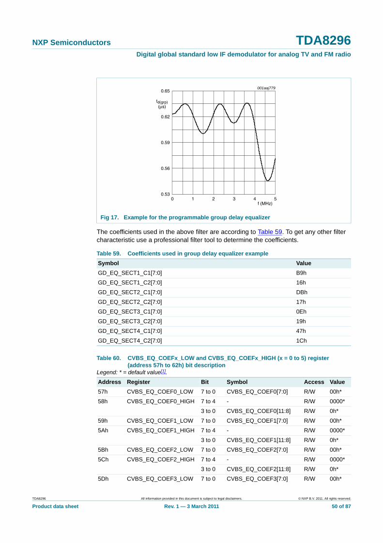
NXP Semiconductors TDA8296Digital global standard low IF demodulator for analog TV and FM radio
The coefficients used in the above filter are according to Table 59. To get any other filter characteristic use a professional filter tool to determine the coefficients.
Fig 17. Example for the programmable group delay equalizer
Table 59. Coefficients used in group delay equalizer example Symbol ValueGD_EQ_SECT1_C1[7:0] B9h
GD_EQ_SECT1_C2[7:0] 16h
GD_EQ_SECT2_C1[7:0] DBh
GD_EQ_SECT2_C2[7:0] 17h
GD_EQ_SECT3_C1[7:0] 0Eh
GD_EQ_SECT3_C2[7:0] 19h
GD_EQ_SECT4_C1[7:0] 47h
GD_EQ_SECT4_C2[7:0] 1Ch
Table 60. CVBS_EQ_COEFx_LOW and CVBS_EQ_COEFx_HIGH (x = 0 to 5) register (address 57h to 62h) bit description
Legend: * = default value[1].
Address Register Bit Symbol Access Value57h CVBS_EQ_COEF0_LOW 7 to 0 CVBS_EQ_COEF0[7:0] R/W 00h*
58h CVBS_EQ_COEF0_HIGH 7 to 4 - R/W 0000*
3 to 0 CVBS_EQ_COEF0[11:8] R/W 0h*
59h CVBS_EQ_COEF1_LOW 7 to 0 CVBS_EQ_COEF1[7:0] R/W 00h*
5Ah CVBS_EQ_COEF1_HIGH 7 to 4 - R/W 0000*
3 to 0 CVBS_EQ_COEF1[11:8] R/W 0h*
5Bh CVBS_EQ_COEF2_LOW 7 to 0 CVBS_EQ_COEF2[7:0] R/W 00h*
5Ch CVBS_EQ_COEF2_HIGH 7 to 4 - R/W 0000*
3 to 0 CVBS_EQ_COEF2[11:8] R/W 0h*
5Dh CVBS_EQ_COEF3_LOW 7 to 0 CVBS_EQ_COEF3[7:0] R/W 00h*
f (MHz)0 542 31
001aaj779
0.59
0.56
0.62
0.65
td(grp)(μs)
0.53
TDA8296 All information provided in this document is subject to legal disclaimers. © NXP B.V. 2011. All rights reserved.
Product data sheet Rev. 1 — 3 March 2011 50 of 87
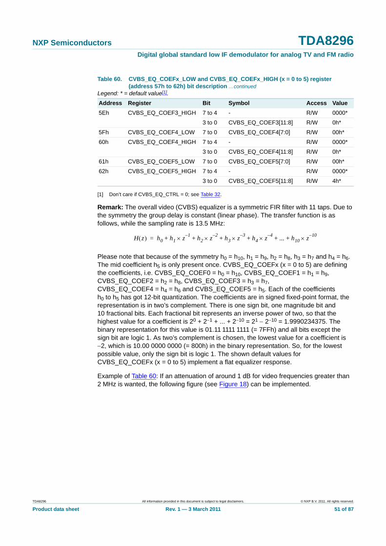
NXP Semiconductors TDA8296Digital global standard low IF demodulator for analog TV and FM radio
[1] Don’t care if CVBS_EQ_CTRL = 0; see Table 32.
Remark: The overall video (CVBS) equalizer is a symmetric FIR filter with 11 taps. Due to the symmetry the group delay is constant (linear phase). The transfer function is as follows, while the sampling rate is 13.5 MHz:
Please note that because of the symmetry h0 = h10, h1 = h9, h2 = h8, h3 = h7 and h4 = h6. The mid coefficient h5 is only present once. CVBS_EQ_COEFx (x = 0 to 5) are defining the coefficients, i.e. CVBS_EQ_COEF0 = h0 = h10, CVBS_EQ_COEF1 = h1 = h9, CVBS_EQ_COEF2 = h2 = h8, CVBS_EQ_COEF3 = h3 = h7, CVBS_EQ_COEF4 = h4 = h6 and CVBS_EQ_COEF5 = h5. Each of the coefficients h0 to h5 has got 12-bit quantization. The coefficients are in signed fixed-point format, the representation is in two’s complement. There is one sign bit, one magnitude bit and 10 fractional bits. Each fractional bit represents an inverse power of two, so that the highest value for a coefficient is 20 + 2−1 + ... + 2−10 = 21 − 2−10 = 1.9990234375. The binary representation for this value is 01.11 1111 1111 (= 7FFh) and all bits except the sign bit are logic 1. As two’s complement is chosen, the lowest value for a coefficient is −2, which is 10.00 0000 0000 (= 800h) in the binary representation. So, for the lowest possible value, only the sign bit is logic 1. The shown default values for CVBS_EQ_COEFx (x = 0 to 5) implement a flat equalizer response.
Example of Table 60: If an attenuation of around 1 dB for video frequencies greater than 2 MHz is wanted, the following figure (see Figure 18) can be implemented.
5Eh CVBS_EQ_COEF3_HIGH 7 to 4 - R/W 0000*
3 to 0 CVBS_EQ_COEF3[11:8] R/W 0h*
5Fh CVBS_EQ_COEF4_LOW 7 to 0 CVBS_EQ_COEF4[7:0] R/W 00h*
60h CVBS_EQ_COEF4_HIGH 7 to 4 - R/W 0000*
3 to 0 CVBS_EQ_COEF4[11:8] R/W 0h*
61h CVBS_EQ_COEF5_LOW 7 to 0 CVBS_EQ_COEF5[7:0] R/W 00h*
62h CVBS_EQ_COEF5_HIGH 7 to 4 - R/W 0000*
3 to 0 CVBS_EQ_COEF5[11:8] R/W 4h*
Table 60. CVBS_EQ_COEFx_LOW and CVBS_EQ_COEFx_HIGH (x = 0 to 5) register (address 57h to 62h) bit description …continued
Legend: * = default value[1].
Address Register Bit Symbol Access Value
H z( ) h0 h1 z 1–× h2 z 2– h3 z 3– h4 z 4– ... h10 z 10–×+ +×+×+×+ +=
TDA8296 All information provided in this document is subject to legal disclaimers. © NXP B.V. 2011. All rights reserved.
Product data sheet Rev. 1 — 3 March 2011 51 of 87
NXP Semiconductors TDA8296Digital global standard low IF demodulator for analog TV and FM radio
Fig 18. Example for the programmable video equalizer
Table 61. Coefficients used in video equalizer example Symbol ValueCVBS_EQ_COEF0[11:0] 005h
CVBS_EQ_COEF1[11:0] FFDh
CVBS_EQ_COEF2[11:0] 016h
CVBS_EQ_COEF3[11:0] FFFh
CVBS_EQ_COEF4[11:0] 018h
CVBS_EQ_COEF5[11:0] 39Ch
f (MHz)751 6420 3
001aaj780
−1.2
−1.6
−0.4
−0.8
0
αresp(f)(dB)
−2.0
TDA8296 All information provided in this document is subject to legal disclaimers. © NXP B.V. 2011. All rights reserved.
Product data sheet Rev. 1 — 3 March 2011 52 of 87
NXP Semiconductors TDA8296Digital global standard low IF demodulator for analog TV and FM radio
10. Limiting values
[1] Stresses above the absolute maximum ratings may cause permanent damage to the device. Exposure to absolute maximum ratings conditions for extended periods may affect device reliability.
[2] Tj depends on the assembly condition of the package and especially on the design of the PCB. The application mounting must be done in such a way that the maximum junction temperature Tj(max) is never exceeded.
[3] No power sequence requirement
[4] Class IV according to EIA/JESD22-C101.
11. Thermal characteristics
The thermal resistance depends strongly on the nature of the PCB used in the application and on its design. The thermal resistance given in Table 63 corresponds to the value that can be measured on a multilayer PCB (4 layers) as defined by EIA/JESD51-2. This value is given for information only.
The junction temperature influences strongly the reliability of an IC. The PCB used in the application contributes on a large part to the overall thermal characteristic. It must therefore be designed to insure that the junction temperature of the IC never exceeds Tj(max) = 125 °C at the maximum ambient temperature.
The IC has to be soldered to ground with its die-attached paddle. Plenty of vias are recommended to remove the heat.
Table 62. Limiting values In accordance with the Absolute Maximum Rating System (IEC 60134).[1][2][3]
Symbol Parameter Conditions Min Max UnitVDDD(1V2) digital supply voltage (1.2 V) −0.5 +1.5 V
VDDDR(3V3) ring digital supply voltage (3.3 V) −0.5 +4.6 V
VDDA(ADC)(1V2) ADC analog supply voltage (1.2 V) −0.5 +1.5 V
VDDA(PLL)(1V2) PLL analog supply voltage (1.2 V) −0.5 +1.5 V
VDDA(DAC)(3V3) DAC analog supply voltage (3.3 V) −0.5 +4.6 V
Vi input voltage pins XIN, IF_POS and IF_NEG
−0.5 +1.3 V
digital input pins −0.5 +4.6 V
Tlead lead temperature - 300 °C
Ptot total power dissipation Tamb = 85 °C - 0.5 W
Tstg storage temperature −40 +125 °C
Tj junction temperature - +125 °C
Tamb ambient temperature −20 +85 °C
VESD electrostatic discharge voltage all pins:
Field ind. Charge Device Model (FCDM)
[4] - ±1000 V
Human Body Model (HBM) - ±4000 V
Table 63. Thermal characteristics Symbol Parameter Conditions Typ UnitRth(j-a) thermal resistance from junction to
ambientin still air 36.8 K/W
TDA8296 All information provided in this document is subject to legal disclaimers. © NXP B.V. 2011. All rights reserved.
Product data sheet Rev. 1 — 3 March 2011 53 of 87
NXP Semiconductors TDA8296Digital global standard low IF demodulator for analog TV and FM radio
12. Characteristics
Table 64. Characteristics Power supplies 3.3 V, 1.2 V; Tamb = 25 °C; PC/SC1 for L and M = 10 dB, all others 13 dB; nominal residual picture carrier of 3 % for L/L’ , 10 % for M, 10 % for B/G, 12.5 % for D/K, 20 % for I; FM/AM modulation = 54 %, 1 kHz modulation frequency; measured in application PCB (see Figure 22 and Figure 23) with 16 MHz crystal frequency, terminated with 75 Ω (CVBS) and 1 kΩ (SSIF/audio). Operation mode set via easy programming (Section 9.3.1), otherwise stated. Low IF input signal at -3dB full scale, input frequencies as defined under row header IF input.
Symbol Parameter Conditions Min Typ Max UnitPower supplyVDD(1V2) supply voltage (1.2 V) digital and analog 1.1 1.2 1.3 V
VDD(3V3) supply voltage (3.3 V) digital and analog 3.0 3.3 3.6 V
IDD(tot)(1V2) total supply current (1.2 V) - 49 - mA
IDD(tot)(3V3) total supply current (3.3 V) - 65 - mA
Ptot total power dissipation default settings; fs = 54 MHz at ADC; DAC application in accordance to Figure 23
- 270 - mW
fs = 54 MHz at ADC; DAC application in accordance to Figure 24
- 150 - mW
Standby mode - 5 8 mW
Digital I/OsVIH HIGH-level input voltage all inputs (except pin XIN);
including voltage on outputs in 3-state mode
0.7 × VDD(3V3) - 6.0 V
VIL LOW-level input voltage all inputs (except pin XIN); including voltage on outputs in 3-state mode
- - 0.8 V
VOH HIGH-level output voltage source current 4 mA VDD(3V3) − 0.4 - - V
VOL LOW-level output voltage sink current 4 mA - - 0.4 V
Ci input capacitance - - 5 pF
Master clockfclk(o)(PLL) PLL output clock frequency [1] - 108 - MHz
Δf/fclk relative frequency deviation from clock frequency
- - ±200 10−6
Reference frequency in Slave modefclk(ext) external clock frequency - 16 - MHz
Vi(RMS) RMS input voltage AC coupled 200 250 - mV
SRr rising slew rate external clock 30 - - mV/ns
tjit(cc) cycle-to-cycle jitter time RMS value - 12.5 - ps
Ci input capacitance on pin XIN - 3 - pF
TDA8296 All information provided in this document is subject to legal disclaimers. © NXP B.V. 2011. All rights reserved.
Product data sheet Rev. 1 — 3 March 2011 54 of 87
NXP Semiconductors TDA8296Digital global standard low IF demodulator for analog TV and FM radio
Reference frequency in Oscillator mode (with a crystal)fxtal crystal frequency - 16 - MHz
Δfxtal/fxtal relative crystal frequency variation
temperature, ageing and spreading
- - ±200 10−6
IF inputVi(p-p) peak-to-peak input voltage for full-scale ADC input
(0 dBFS)0.7 0.8 0.9 V
Ri(dif) differential input resistance 10 15 - kΩ
Ci(dif) differential input capacitance
- 2 3 pF
Vi input voltage operational input related to ADC full scale; all standards; sum of all signals
−3 −3 −3 dBFS
fi input frequency PC / SC1
M/N standard - 5.40 / 0.90 - MHz
B standard - 6.40 / 0.90 - MHz
G/H standard - 6.75 / 1.25 - MHz
I standard - 7.25 / 1.25 - MHz
D/K standard - 6.85 / 0.35 - MHz
L standard - 6.75 / 0.25 - MHz
L-accent standard - 1.25 / 7.75 - MHz
FM radio - 1.25 - MHz
IF selectivityαsup(stpb) stop-band suppression Hilbert filter stop-band −60 - - dB
decimation filter stop-band −40 - - dB
notch for NSC (NPC for L-accent standard)
[2] −40 - - dB
Carrier recovery FPLLB−3dB(cl) closed-loop −3 dB
bandwidthultrawide - 280 - kHz
superwide - 130 - kHz
wide - 60 - kHz
medium - 30 - kHz
narrow - 15 - kHz
Δfpullin pull-in frequency range [3] - ±830 - kHz
mover(PC) picture carrier over modulation index
black for L/L-accent standard; flat field white else
115 117 - %
fstep(AFC) AFC step frequency 128 steps [3] 13 - - kHz
Table 64. Characteristics …continuedPower supplies 3.3 V, 1.2 V; Tamb = 25 °C; PC/SC1 for L and M = 10 dB, all others 13 dB; nominal residual picture carrier of 3 % for L/L’ , 10 % for M, 10 % for B/G, 12.5 % for D/K, 20 % for I; FM/AM modulation = 54 %, 1 kHz modulation frequency; measured in application PCB (see Figure 22 and Figure 23) with 16 MHz crystal frequency, terminated with 75 Ω (CVBS) and 1 kΩ (SSIF/audio). Operation mode set via easy programming (Section 9.3.1), otherwise stated. Low IF input signal at -3dB full scale, input frequencies as defined under row header IF input.
Symbol Parameter Conditions Min Typ Max Unit
TDA8296 All information provided in this document is subject to legal disclaimers. © NXP B.V. 2011. All rights reserved.
Product data sheet Rev. 1 — 3 March 2011 55 of 87
NXP Semiconductors TDA8296Digital global standard low IF demodulator for analog TV and FM radio
IF demodulation (video equalizer in Flat mode)BT(tot) total transition bandwidth Nyquist filter; all standards - 1 - MHz
αsup(stpb) stop-band suppression Nyquist filter; all standards −60 - - dB
video low-pass filter (M/N, B/G/H, I, D/K, L/L-accent standard)
- −60 - dB
Bvideo(−1dB) −1 dB video bandwidth M/N standard - 3.8 - MHz
B/G/H, I, D/K, L/L-accent standard
- 4.8 - MHz
tripple(GDE) group delay equalizer ripple time
peak value for B/G/H half, D/K half, I flat, M (FCC) full, L/L-accent full standard
- 20 40 ns
Digital IF AGC (internal loop)B−3dB(cl) closed-loop −3 dB
bandwidthnegative modulation (all standards except L/L-accent)
[4] 400 - - Hz
positive modulation (L/L-accent standard)
0.2 - - Hz
tresp response time ±20 dB level change; video settled within ±3 dB
negative modulation (all standards except L/L-accent)
- 3 - ms
positive modulation (L/L-accent standard)
- 100 - ms
ΔGAGC AGC gain range −20 - +48 dB
Tuner IF AGC (external loop)tresp response time at 60 dBμV (RMS) PC input;
±20 dB level change; video settled within ±3 dB
[5]
with TDA1827x; positive modulation
- 3 000 - ms
with TDA1827x; negative modulation
- 600 - ms
f−3dB(lpf) low-pass filter −3 dB frequency
IF AGC postfilter 0.9 1.0 1.1 kHz
Table 64. Characteristics …continuedPower supplies 3.3 V, 1.2 V; Tamb = 25 °C; PC/SC1 for L and M = 10 dB, all others 13 dB; nominal residual picture carrier of 3 % for L/L’ , 10 % for M, 10 % for B/G, 12.5 % for D/K, 20 % for I; FM/AM modulation = 54 %, 1 kHz modulation frequency; measured in application PCB (see Figure 22 and Figure 23) with 16 MHz crystal frequency, terminated with 75 Ω (CVBS) and 1 kΩ (SSIF/audio). Operation mode set via easy programming (Section 9.3.1), otherwise stated. Low IF input signal at -3dB full scale, input frequencies as defined under row header IF input.
Symbol Parameter Conditions Min Typ Max Unit
TDA8296 All information provided in this document is subject to legal disclaimers. © NXP B.V. 2011. All rights reserved.
Product data sheet Rev. 1 — 3 March 2011 56 of 87
NXP Semiconductors TDA8296Digital global standard low IF demodulator for analog TV and FM radio
CVBS outputVo(p-p) peak-to-peak output
voltagenegative PC modulation (all standards except L/L-accent); 75 Ω DC load; sync-white modulation
65 % - 0.7 - V
nominal 0.9 1.0 1.1 V
115 % - 1.0 - V
positive PC modulation (L/L-accent standard); 75 Ω DC load; sync-white modulation
65 % - 0.7 - V
nominal 0.9 1.0 1.1 V
115 % - 1.0 - V
Bvideo(−3dB) −3 dB video bandwidth overall video response; CVBS equalizer flat
all standards except M/N 4.7 4.85 - MHz
M/N standard 3.8 3.9 - MHz
αresp(f) frequency response video equalizer; 8 equally spaced settings; value at 3.9 MHz
−5 - +4.5 dB
Gdif differential gain “ITU-T J.63 line 330” [6] - 1.5 5 %
ϕdif differential phase “ITU-T J.63 line 330” - 1.0 3 deg
Vvideo/Vsync video voltage to sync voltage ratio
video DAC application according to Figure 23
1.9 2.33 3.0
Vsync synchronization voltage video DAC application according to Figure 23
160 200 240 mV
Vstlt/VCVBS(p-p) synchronization tilt voltage to peak-to-peak CVBS voltage ratio
- 1 2 %
Vftlt/VCVBS(p-p) frame tilt voltage to peak-to-peak CVBS voltage ratio
all standards except L/L-accent
- 1 3 %
L/L-accent standard in peak white AGC detection
- 1 5 %
ΔVtro/Vtro relative transient response overshoot voltage variation
2T pulse [7] - 2 5 %
Table 64. Characteristics …continuedPower supplies 3.3 V, 1.2 V; Tamb = 25 °C; PC/SC1 for L and M = 10 dB, all others 13 dB; nominal residual picture carrier of 3 % for L/L’ , 10 % for M, 10 % for B/G, 12.5 % for D/K, 20 % for I; FM/AM modulation = 54 %, 1 kHz modulation frequency; measured in application PCB (see Figure 22 and Figure 23) with 16 MHz crystal frequency, terminated with 75 Ω (CVBS) and 1 kΩ (SSIF/audio). Operation mode set via easy programming (Section 9.3.1), otherwise stated. Low IF input signal at -3dB full scale, input frequencies as defined under row header IF input.
Symbol Parameter Conditions Min Typ Max Unit
TDA8296 All information provided in this document is subject to legal disclaimers. © NXP B.V. 2011. All rights reserved.
Product data sheet Rev. 1 — 3 March 2011 57 of 87

NXP Semiconductors TDA8296Digital global standard low IF demodulator for analog TV and FM radio
αIM(blue) intermodulation suppression (blue)
carrier levels related to PC sync; PC = −3.2 dB; CC = −19.2 dB; SC = −13 dB
1.1 MHz (related to black-to-white in RMS, equals CC + 3.6 dB)
- 67 - dB
3.3 MHz (related to CC) - 77 - dB
αIM(yellow) intermodulation suppression (yellow)
carrier levels related to PC sync; PC = −10 dB; CC = −19.2 dB; SC = −13 dB
1.1 MHz (related to black-to-white in RMS, equals CC + 3.6 dB)
- 70 - dB
3.3 MHz (related to CC) - 78 - dB
(S/N)w weighted signal-to-noise ratio
all standards; unified weighting filter (“ITU-T J.61”); PC at −6 dBFS
57 60 - dB
PSRR power supply rejection ratio fripple = 70 Hz; 100 mV (p-p); video signal: gray; level: 50 %; TDA8296 stand alone; input
positive video modulation; L standard; 1.2 V
- 39 - dB
positive video modulation; L standard; 3.3 V
[8] - 47 - dB
negative video modulation; B standard; 1.2 V
- 65 - dB
negative video modulation; B standard; 3.3 V
[8] - 37 - dB
αsup(f)L(unw) unwanted leakage frequency suppression
4.8 MHz video modulation; related to black-to-white in 10 MHz to 200 MHz band, wanted signal (peak-to-peak) and unwanted signal (RMS)
- 56 - dB
Table 64. Characteristics …continuedPower supplies 3.3 V, 1.2 V; Tamb = 25 °C; PC/SC1 for L and M = 10 dB, all others 13 dB; nominal residual picture carrier of 3 % for L/L’ , 10 % for M, 10 % for B/G, 12.5 % for D/K, 20 % for I; FM/AM modulation = 54 %, 1 kHz modulation frequency; measured in application PCB (see Figure 22 and Figure 23) with 16 MHz crystal frequency, terminated with 75 Ω (CVBS) and 1 kΩ (SSIF/audio). Operation mode set via easy programming (Section 9.3.1), otherwise stated. Low IF input signal at -3dB full scale, input frequencies as defined under row header IF input.
Symbol Parameter Conditions Min Typ Max Unit
TDA8296 All information provided in this document is subject to legal disclaimers. © NXP B.V. 2011. All rights reserved.
Product data sheet Rev. 1 — 3 March 2011 58 of 87

NXP Semiconductors TDA8296Digital global standard low IF demodulator for analog TV and FM radio
SSIF/mono sound outputfo(SSIF) SSIF output frequency SC1 or FM radio carrier [9]
M standard - 4.5 - MHz
B/G/H standard - 5.5 - MHz
I standard - 6.0 - MHz
D/K/L/L-accent standard - 6.5 - MHz
FM radio - 5.5 - MHz
Vo(SSIF)(RMS) RMS SSIF output voltage 1 kΩ DC or AC load; no modulation; PC / SC1 = 13 dB; Cs = 220 pF
M standard 105 120 135 mV
B standard 100 115 130 mV
G/H standard 100 115 130 mV
D/K standard 95 110 125 mV
I standard 100 115 130 mV
L standard 95 110 125 mV
L-accent standard 95 110 125 mV
FM radio (single carrier) 100 115 130 mV
Vo(AF)(RMS) RMS AF output voltage 1 kΩ DC or AC load; FM; gain 0 dB
M standard; 54 % modulation degree (±13.5 kHz FM deviation before pre-emphasis)
98 126 135 mV
B, G/H, I, D/K standard; 54 % modulation degree (±27 kHz FM deviation before pre-emphasis)
107 133 144 mV
L/L-accent standard; AM; m = 54 %; gain +6 dB
158 176 196 mV
FM radio; 30 % modulation degree (±22.5 kHz FM deviation before pre-emphasis)
51 54 60 mV
high Deviation mode (D/K standard China); FM deviation before pre-emphasis ±400 kHz; sound level setting: −12 dB
[10] - 425 - mV
Table 64. Characteristics …continuedPower supplies 3.3 V, 1.2 V; Tamb = 25 °C; PC/SC1 for L and M = 10 dB, all others 13 dB; nominal residual picture carrier of 3 % for L/L’ , 10 % for M, 10 % for B/G, 12.5 % for D/K, 20 % for I; FM/AM modulation = 54 %, 1 kHz modulation frequency; measured in application PCB (see Figure 22 and Figure 23) with 16 MHz crystal frequency, terminated with 75 Ω (CVBS) and 1 kΩ (SSIF/audio). Operation mode set via easy programming (Section 9.3.1), otherwise stated. Low IF input signal at -3dB full scale, input frequencies as defined under row header IF input.
Symbol Parameter Conditions Min Typ Max Unit
TDA8296 All information provided in this document is subject to legal disclaimers. © NXP B.V. 2011. All rights reserved.
Product data sheet Rev. 1 — 3 March 2011 59 of 87

NXP Semiconductors TDA8296Digital global standard low IF demodulator for analog TV and FM radio
αhr(AF) AF headroom before clipping; 1 kΩ DC or AC load
M standard; related to ±25 kHz peak deviation before pre-emphasis
- 7 - dB
B, G/H, I, D/K standard; related to ±50 kHz peak deviation before pre-emphasis
- 7 - dB
L/L-accent standard; PC / SC1 ratio for start of audio output clipping; AM; m = 100 %; related to mean SC1
- 9 - dB
FM radio; 30 % modulation degree related to ±22.5 kHz peak deviation before pre-emphasis
- 9 - dB
τdeemp de-emphasis time constant M/N standard (mono); FM radio USA
- 75 - μs
B/G/H, I, D/K standard; FM radio Europe
- 50 - μs
B−3dB −3 dB bandwidth audio low-pass filter
L/L-accent standard - 30 - kHz
M-BTSC standard - 140 - kHz
THD total harmonic distortion FM; for 50 kHz deviation before pre-emphasis (25 kHz for M standard)
- 0.15 0.3 %
AM; m = 80 % - 0.5 1 %
BAF(−3dB) −3 dB AF bandwidth AM 20 27 - kHz
FM 40 50 - kHz
αAM AM suppression of FM demodulator; AM: f = 1 kHz; m = 54 % referenced to 27 kHz FM deviation
40 51 - dB
Table 64. Characteristics …continuedPower supplies 3.3 V, 1.2 V; Tamb = 25 °C; PC/SC1 for L and M = 10 dB, all others 13 dB; nominal residual picture carrier of 3 % for L/L’ , 10 % for M, 10 % for B/G, 12.5 % for D/K, 20 % for I; FM/AM modulation = 54 %, 1 kHz modulation frequency; measured in application PCB (see Figure 22 and Figure 23) with 16 MHz crystal frequency, terminated with 75 Ω (CVBS) and 1 kΩ (SSIF/audio). Operation mode set via easy programming (Section 9.3.1), otherwise stated. Low IF input signal at -3dB full scale, input frequencies as defined under row header IF input.
Symbol Parameter Conditions Min Typ Max Unit
TDA8296 All information provided in this document is subject to legal disclaimers. © NXP B.V. 2011. All rights reserved.
Product data sheet Rev. 1 — 3 March 2011 60 of 87
NXP Semiconductors TDA8296Digital global standard low IF demodulator for analog TV and FM radio
(S/N)w(AF)
AF weighted signal-to-noise ratio
via internal mono sound demodulator; “ITU-R BS.468-4”; FM mode related to 27 kHz deviation before pre-emphasis; 10 % residual PC; SC1
black picture 52 54 - dB
flat field white picture 52 54 - dB
6 kHz sine wave picture 52 54 - dB
250 kHz square wave picture
52 54 - dB
crosshatch picture 52 54 - dB
color bar picture 52 54 - dB
via internal mono sound demodulator; (audio gain +6 dB) “ITU-R BS.468-4”; AM; m = 54 %; 3 % residual PC; SC1
[11]
black picture 40 44 - dB
flat field white picture 41 44 - dB
color bar picture 40 44 - dB
via internal mono sound demodulator; “ITU-R BS.468-4”; FM Radio mode; 22.5 kHz deviation
- 45 - dB
Table 64. Characteristics …continuedPower supplies 3.3 V, 1.2 V; Tamb = 25 °C; PC/SC1 for L and M = 10 dB, all others 13 dB; nominal residual picture carrier of 3 % for L/L’ , 10 % for M, 10 % for B/G, 12.5 % for D/K, 20 % for I; FM/AM modulation = 54 %, 1 kHz modulation frequency; measured in application PCB (see Figure 22 and Figure 23) with 16 MHz crystal frequency, terminated with 75 Ω (CVBS) and 1 kΩ (SSIF/audio). Operation mode set via easy programming (Section 9.3.1), otherwise stated. Low IF input signal at -3dB full scale, input frequencies as defined under row header IF input.
Symbol Parameter Conditions Min Typ Max Unit
TDA8296 All information provided in this document is subject to legal disclaimers. © NXP B.V. 2011. All rights reserved.
Product data sheet Rev. 1 — 3 March 2011 61 of 87
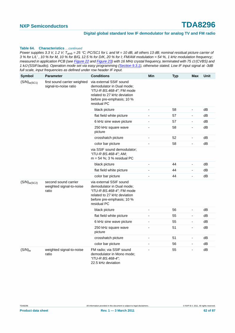
NXP Semiconductors TDA8296Digital global standard low IF demodulator for analog TV and FM radio
(S/N)w(SC1) first sound carrier weighted signal-to-noise ratio
via external SSIF sound demodulator in Dual mode; “ITU-R BS.468-4”; FM mode related to 27 kHz deviation before pre-emphasis; 10 % residual PC
black picture - 58 - dB
flat field white picture - 57 - dB
6 kHz sine wave picture - 57 - dB
250 kHz square wave picture
- 58 - dB
crosshatch picture - 52 - dB
color bar picture - 58 - dB
via SSIF sound demodulator; “ITU-R BS.468-4”; AM; m = 54 %; 3 % residual PC
black picture - 44 - dB
flat field white picture - 44 - dB
color bar picture - 44 - dB
(S/N)w(SC2) second sound carrier weighted signal-to-noise ratio
via external SSIF sound demodulator in Dual mode; “ITU-R BS.468-4”; FM mode related to 27 kHz deviation before pre-emphasis; 10 % residual PC
black picture - 56 - dB
flat field white picture - 55 - dB
6 kHz sine wave picture - 55 - dB
250 kHz square wave picture
- 51 - dB
crosshatch picture - 51 - dB
color bar picture - 56 - dB
(S/N)w weighted signal-to-noise ratio
FM radio; via SSIF sound demodulator in Mono mode; “ITU-R BS.468-4”; 22.5 kHz deviation
- 55 - dB
Table 64. Characteristics …continuedPower supplies 3.3 V, 1.2 V; Tamb = 25 °C; PC/SC1 for L and M = 10 dB, all others 13 dB; nominal residual picture carrier of 3 % for L/L’ , 10 % for M, 10 % for B/G, 12.5 % for D/K, 20 % for I; FM/AM modulation = 54 %, 1 kHz modulation frequency; measured in application PCB (see Figure 22 and Figure 23) with 16 MHz crystal frequency, terminated with 75 Ω (CVBS) and 1 kΩ (SSIF/audio). Operation mode set via easy programming (Section 9.3.1), otherwise stated. Low IF input signal at -3dB full scale, input frequencies as defined under row header IF input.
Symbol Parameter Conditions Min Typ Max Unit
TDA8296 All information provided in this document is subject to legal disclaimers. © NXP B.V. 2011. All rights reserved.
Product data sheet Rev. 1 — 3 March 2011 62 of 87
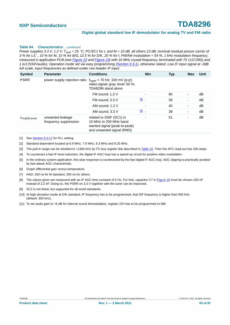
NXP Semiconductors TDA8296Digital global standard low IF demodulator for analog TV and FM radio
[1] See Section 9.3.17 for PLL setting.
[2] Standard dependent located at 6.9 MHz, 7.9 MHz, 8.3 MHz and 9.25 MHz.
[3] The pull-in range can be doubled to ±1 660 kHz by I2C-bus register like described in Table 16. Then the AFC read-out has 256 steps.
[4] To counteract a fast IF level reduction, the digital IF AGC loop has a speed-up circuit for positive video modulation.
[5] In the ordinary system application, this slow response is counteracted by the fast digital IF AGC loop. ADC clipping is practically avoided by fast-attack AGC characteristic.
[6] Graph differential gain versus temperature.
[7] HAD: 250 ns for M standard, 200 ns for others.
[8] The values given are measured with an IF AGC time constant of 5 Hz. For that, capacitor C7 in Figure 19 must be chosen 220 nF instead of 2.2 nF. Doing so, the PSRR on 3.3 V together with the tuner can be improved.
[9] SC2 is not listed, but supported for all world standards.
[10] At high deviation mode at D/K standard, IF frequency has to be programmed, that SIF frequency is higher than 500 kHz (default: 350 kHz).
[11] To set audio gain to +6 dB for internal sound demodulation, register 22h has to be programmed to 08h.
PSRR power supply rejection ratio fripple = 70 Hz; 100 mV (p-p); video signal: gray; level: 50 %; TDA8296 stand alone
FM sound; 1.2 V - 80 - dB
FM sound; 3.3 V [8] - 39 - dB
AM sound; 1.2 V - 40 - dB
AM sound; 3.3 V [8] - 38 - dB
αsup(f)L(unw) unwanted leakage frequency suppression
related to SSIF (SC1) in 10 MHz to 200 MHz band wanted signal (peak-to-peak) and unwanted signal (RMS)
- 51 - dB
Table 64. Characteristics …continuedPower supplies 3.3 V, 1.2 V; Tamb = 25 °C; PC/SC1 for L and M = 10 dB, all others 13 dB; nominal residual picture carrier of 3 % for L/L’ , 10 % for M, 10 % for B/G, 12.5 % for D/K, 20 % for I; FM/AM modulation = 54 %, 1 kHz modulation frequency; measured in application PCB (see Figure 22 and Figure 23) with 16 MHz crystal frequency, terminated with 75 Ω (CVBS) and 1 kΩ (SSIF/audio). Operation mode set via easy programming (Section 9.3.1), otherwise stated. Low IF input signal at -3dB full scale, input frequencies as defined under row header IF input.
Symbol Parameter Conditions Min Typ Max Unit
TDA8296 All information provided in this document is subject to legal disclaimers. © NXP B.V. 2011. All rights reserved.
Product data sheet Rev. 1 — 3 March 2011 63 of 87
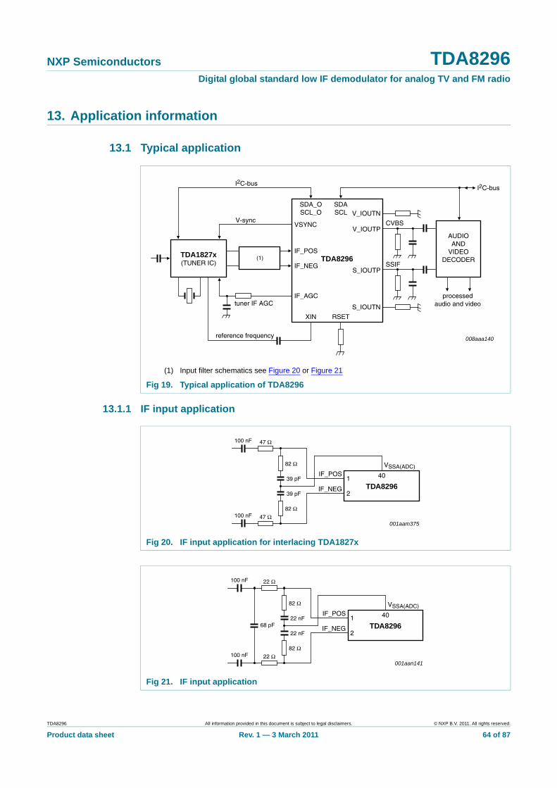
NXP Semiconductors TDA8296Digital global standard low IF demodulator for analog TV and FM radio
13. Application information
13.1 Typical application
13.1.1 IF input application
(1) Input filter schematics see Figure 20 or Figure 21
Fig 19. Typical application of TDA8296
008aaa140
VSYNC
XIN RSET
SDA_OSCL_O
SDASCL
processedaudio and video
TDA1827x(TUNER IC)
AUDIOAND
VIDEODECODERTDA8296
IF_POS
IF_NEG
IF_AGC
S_IOUTN
V_IOUTN
V_IOUTP
S_IOUTPSSIF
CVBS
tuner IF AGC
(1)
reference frequency
V-sync
I2C-busI2C-bus
Fig 20. IF input application for interlacing TDA1827x
Fig 21. IF input application
001aam375
47 Ω
82 Ω
82 Ω
1
VSSA(ADC)
40
2
IF_POS
IF_NEG
100 nF
47 Ω100 nF
39 pF
39 pF
TDA8296
001aan141
22 Ω
82 Ω
82 Ω
1
VSSA(ADC)
40
2
IF_POS
IF_NEG
100 nF
22 Ω100 nF
22 nF
22 nF68 pF TDA8296
TDA8296 All information provided in this document is subject to legal disclaimers. © NXP B.V. 2011. All rights reserved.
Product data sheet Rev. 1 — 3 March 2011 64 of 87
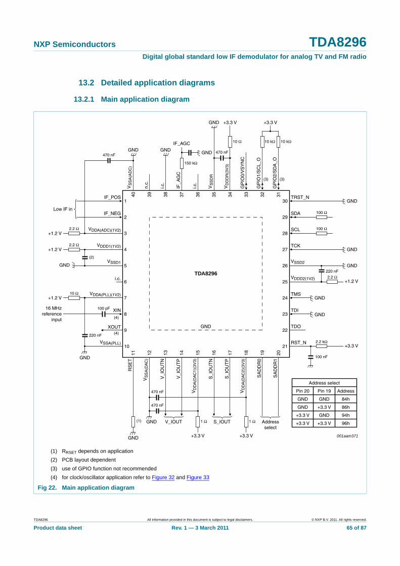
NXP Semiconductors TDA8296Digital global standard low IF demodulator for analog TV and FM radio
13.2 Detailed application diagrams
13.2.1 Main application diagram
(1) RRSET depends on application(2) PCB layout dependent(3) use of GPIO function not recommended(4) for clock/oscillator application refer to Figure 32 and Figure 33
Fig 22. Main application diagram
001aam371
100 Ω
100 Ω
2.2 Ω
2.2 kΩ
10 Ω
1 Ω 1 Ω
10 kΩ10 kΩ10 Ω
150 kΩ
2.2 Ω
2.2 Ω
220 nF
(2)
(1)
(4)
(4)
(3) (3)
220 nF
100 nF
470 nF
470 nF
100 pF
470 nF470 nF
1TRST_N
30IF_POS
GND
GND
GND
GND
GND +3.3 V +3.3 V
GND
2SDA
29IF_NEG
Low IF in
3SCL
28VDDA(ADC)(1V2)
4TCK
27VDDD1(1V2)
5VSSD2
26VSSD1
6VDDD2(1V2)
25i.c.
7TMS
24VDDA(PLL)(1V2)
8TDI
23XIN
+1.2 V
+1.2 V
+1.2 V
16 MHzreference
input
GND9
TDO22
XOUT
10
GND
V_IOUT
+3.3 V +3.3 V
S_IOUT Addressselect
Address select
AddressPin 19Pin 20
84hGNDGND
86h+3.3 VGND
94hGND+3.3 V
96h+3.3 V+3.3 VGND
RST_N+3.3 V
GND
GND
GND
GND
GND
+1.2 V
21VSSA(PLL)
11V
SS
A(A
DC
)40
RS
ET
12n.
c.39
VS
SA
(DA
C)
13i.c
.38
V_I
OU
TN
14IF
_AG
C
IF_AGC
37V
_IO
UT
P
15i.c
.36
VD
DA
(DA
C1)
(3V
3)
16V
SS
DR
35S
_IO
UT
N
17V
DD
DR
(3V
3)34
S_I
OU
TP
18G
PIO
0/V
SY
NC
33V
DD
A(D
AC
2)(3
V3)
19G
PIO
1/S
CL_
O32
SA
DD
R0
20G
PIO
2/S
DA
_O31
SA
DD
R1
TDA8296
TDA8296 All information provided in this document is subject to legal disclaimers. © NXP B.V. 2011. All rights reserved.
Product data sheet Rev. 1 — 3 March 2011 65 of 87
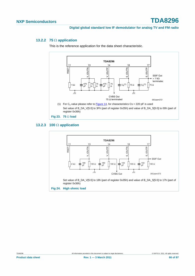
NXP Semiconductors TDA8296Digital global standard low IF demodulator for analog TV and FM radio
13.2.2 75 Ω applicationThis is the reference application for the data sheet characteristic.
13.2.3 100 Ω application
(1) For Cs value please refer to Figure 14, for characteristics Cs = 220 pF is usedSet value of B_DA_V[5:0] to 3Fh (part of register 0x35h) and value of B_DA_S[5:0] to 00h (part of register 0x36h)
Fig 23. 75 Ω load
001aam372
1 kΩ 75 Ω75Ω Cs(1)75
Ω75Ω
470pF
470pF
RS
ET
V_I
OU
TN
S_I
OU
TN
75 ΩCs(1)
S_I
OU
TP
V_I
OU
TP
11 13 16 17
CVBS Out75 Ω terminated
SSIF Out> 1 kΩterminated
14
TDA8296
Set value of B_DA_V[5:0] to 18h (part of register 0x35h) and value of B_DA_S[5:0] to 17h (part of register 0x36h)
Fig 24. High ohmic load
001aam373
2 kΩ 100 Ω100 Ω 150pF
100 Ω180pF
180pF
RS
ET
V_I
OU
TN
S_I
OU
TN
100 Ω150pF
S_I
OU
TP
V_I
OU
TP
11 13 16 17
CVBS Out
SSIF Out
14
TDA8296
TDA8296 All information provided in this document is subject to legal disclaimers. © NXP B.V. 2011. All rights reserved.
Product data sheet Rev. 1 — 3 March 2011 66 of 87

NXP Semiconductors TDA8296Digital global standard low IF demodulator for analog TV and FM radio
13.2.4 Buffer application
13.2.5 Layout recommendations
Set value of B_DA_V[5:0] to 18h (part of register 0x35h) and value of B_DA_S[5:0] to 17h (part of register 0x36h)
Fig 25. Buffer application with 75 Ω load
001aam374
33 Ω2 kΩ 100 Ω 100Ω
150pF
33 Ω 33 Ω
200 Ω
150 Ω
150 Ω
560 Ω
PBSS2515VS
PBSS4140U
CVBS75 Ohm(SCART)
+5 V
VIDEODECODER
68 Ω
220pF
150pF
47 μF
RS
ET
V_I
OU
TN
S_I
OU
TN
S_I
OU
TP
V_I
OU
TP
11 13 16 17
SSIF Out
14
TDA8296
100 nF
(1) Bottom layer(2) Top layer
Fig 26. PCB pattern using circuit diagrams of Figure 20, Figure 22, Figure 23 and 16 MHz reference from XTAL
001aam882001aam882
SDA
SDA-T
SCL-T
IF-AGC
Low-IFp
Low-IFnSCL
SIFp
CVBSp
470
pF
75 Ω
2.2 Ω
47 Ω
47 Ω
82 Ω
82 Ω
39 pF
39 pF
2.2 Ω
10 Ω
100 Ω
100 Ω
470
pF
270
pF
75 Ω
75 Ω
270
pF
470
nF
470
nF
1 nF
150
kΩ
4.7
kΩ
4.7
kΩ
4.7
kΩ
4.7
kΩ
10 Ω
2.2 Ω
1.0 Ω
1.0 Ω
470 nF
470 nF
470
nF47
0 nF
18 p
F18
pF
16 MHz
n.c.
n.c.n.c.
1.0
kΩ
TDA8296HN
18.00
18.00
75 Ω
75 Ω
(1)
(2)
TDA8296 All information provided in this document is subject to legal disclaimers. © NXP B.V. 2011. All rights reserved.
Product data sheet Rev. 1 — 3 March 2011 67 of 87
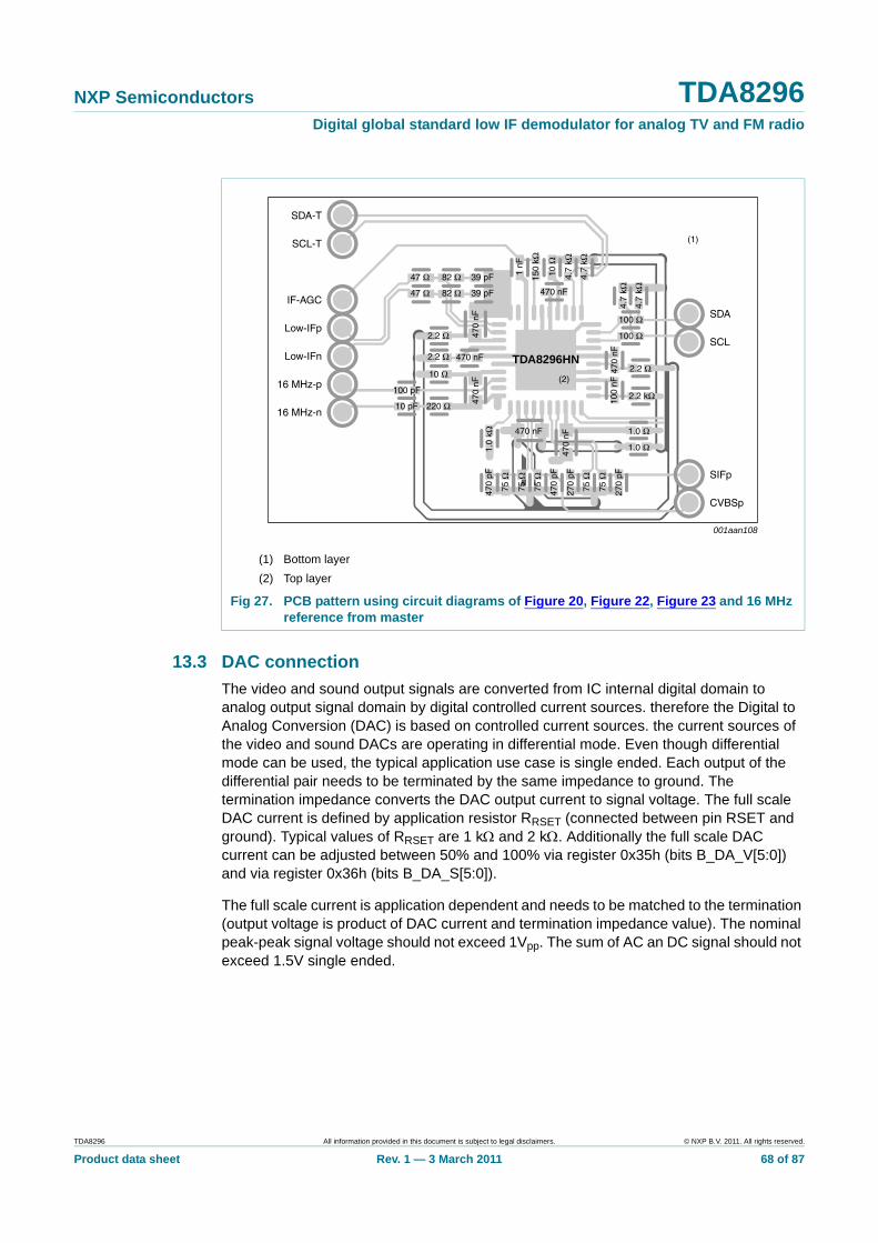
NXP Semiconductors TDA8296Digital global standard low IF demodulator for analog TV and FM radio
13.3 DAC connectionThe video and sound output signals are converted from IC internal digital domain to analog output signal domain by digital controlled current sources. therefore the Digital to Analog Conversion (DAC) is based on controlled current sources. the current sources of the video and sound DACs are operating in differential mode. Even though differential mode can be used, the typical application use case is single ended. Each output of the differential pair needs to be terminated by the same impedance to ground. The termination impedance converts the DAC output current to signal voltage. The full scale DAC current is defined by application resistor RRSET (connected between pin RSET and ground). Typical values of RRSET are 1 kΩ and 2 kΩ. Additionally the full scale DAC current can be adjusted between 50% and 100% via register 0x35h (bits B_DA_V[5:0]) and via register 0x36h (bits B_DA_S[5:0]).
The full scale current is application dependent and needs to be matched to the termination (output voltage is product of DAC current and termination impedance value). The nominal peak-peak signal voltage should not exceed 1Vpp. The sum of AC an DC signal should not exceed 1.5V single ended.
(1) Bottom layer(2) Top layer
Fig 27. PCB pattern using circuit diagrams of Figure 20, Figure 22, Figure 23 and 16 MHz reference from master
001aan108
SDA-T
SCL-T
SDA
SCL
TDA8296HN
SIFp
CVBSp
IF-AGC
Low-IFp
Low-IFn
16 MHz-p
16 MHz-n
470
pF
75 Ω
2.2 Ω
2.2 Ω
10 Ω
220 Ω10 pF
100 pF
47 Ω
47 Ω
82 Ω
82 Ω
39 pF
39 pF
100 Ω
100 Ω
470
pF
270
pF
75 Ω
75 Ω
270
pF
470
nF
470
nF
1 nF
150
kΩ
4.7
kΩ
4.7
kΩ
4.7
kΩ
4.7
kΩ
10 Ω
2.2 Ω
1.0 Ω
1.0 Ω
470 nF
470 nF
470
nF47
0 nF
470 nF
2.2 kΩ
100
nF
1.0
kΩ
75 Ω
75 Ω
(1)
(2)
TDA8296 All information provided in this document is subject to legal disclaimers. © NXP B.V. 2011. All rights reserved.
Product data sheet Rev. 1 — 3 March 2011 68 of 87
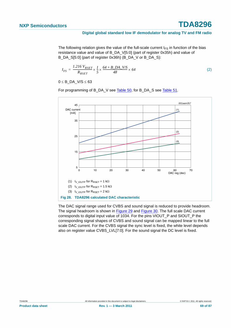
NXP Semiconductors TDA8296Digital global standard low IF demodulator for analog TV and FM radio
The following relation gives the value of the full-scale current IFS in function of the bias resistance value and value of B_DA_V[5:0] (part of register 0x35h) and value of B_DA_S[5:0] (part of register 0x36h) (B_DA_V or B_DA_S):
(2)
0 ≤ B_DA_V/S ≤ 63
For programming of B_DA_V see Table 50, for B_DA_S see Table 51.
The DAC signal range used for CVBS and sound signal is reduced to provide headroom. The signal headroom is shown in Figure 29 and Figure 30. The full scale DAC current corresponds to digital input value of 1034. For the pins VIOUT_P and SIOUT_P the corresponding signal shapes of CVBS and sound signal can be mapped linear to the full scale DAC current. For the CVBS signal the sync level is fixed, the white level depends also on register value CVBS_LVL[7:0]. For the sound signal the DC level is fixed.
(1) IV_IOUTP for RRSET = 1 kΩ
(2) IV_IOUTP for RRSET = 1.5 kΩ
(3) IV_IOUTP for RRSET = 2 kΩ
Fig 28. TDA8296 calculated DAC characteristic
IFS1.216 VRSET
RRSET------------------------------ 1
5---× 64 B_DA_V/S+
48--------------------------------------× 64×=
DAC reg (dec)0 30 7010 5040 6020
001aam35745
5
15
25
35
DAC current[mA]
(1)
(2)
(3)
TDA8296 All information provided in this document is subject to legal disclaimers. © NXP B.V. 2011. All rights reserved.
Product data sheet Rev. 1 — 3 March 2011 69 of 87
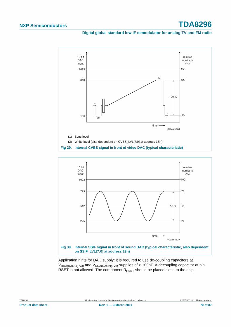
NXP Semiconductors TDA8296Digital global standard low IF demodulator for analog TV and FM radio
Application hints for DAC supply: it is required to use de-coupling capacitors at VDDA(DAC1)(3V3) and VDDA(DAC2)(3V3) supplies of > 100nF. A decoupling capacitor at pin RSET is not allowed. The component RRSET should be placed close to the chip.
(1) Sync level(2) White level (also dependent on CVBS_LVL[7:0] at address 1Eh)
Fig 29. Internal CVBS signal in front of video DAC (typical characteristic)
Fig 30. Internal SSIF signal in front of sound DAC (typical characteristic, also dependent on SSIF_LVL[7:0] at address 23h)
time
20
120(2)
(1)
1501023
818
136
100 %
10 bitDACinput
relativenumbers
(%)
001aam628
time
22
50
78
1001023
799
512
225
56 %
10 bitDACinput
relativenumbers
(%)
001aam629
TDA8296 All information provided in this document is subject to legal disclaimers. © NXP B.V. 2011. All rights reserved.
Product data sheet Rev. 1 — 3 March 2011 70 of 87
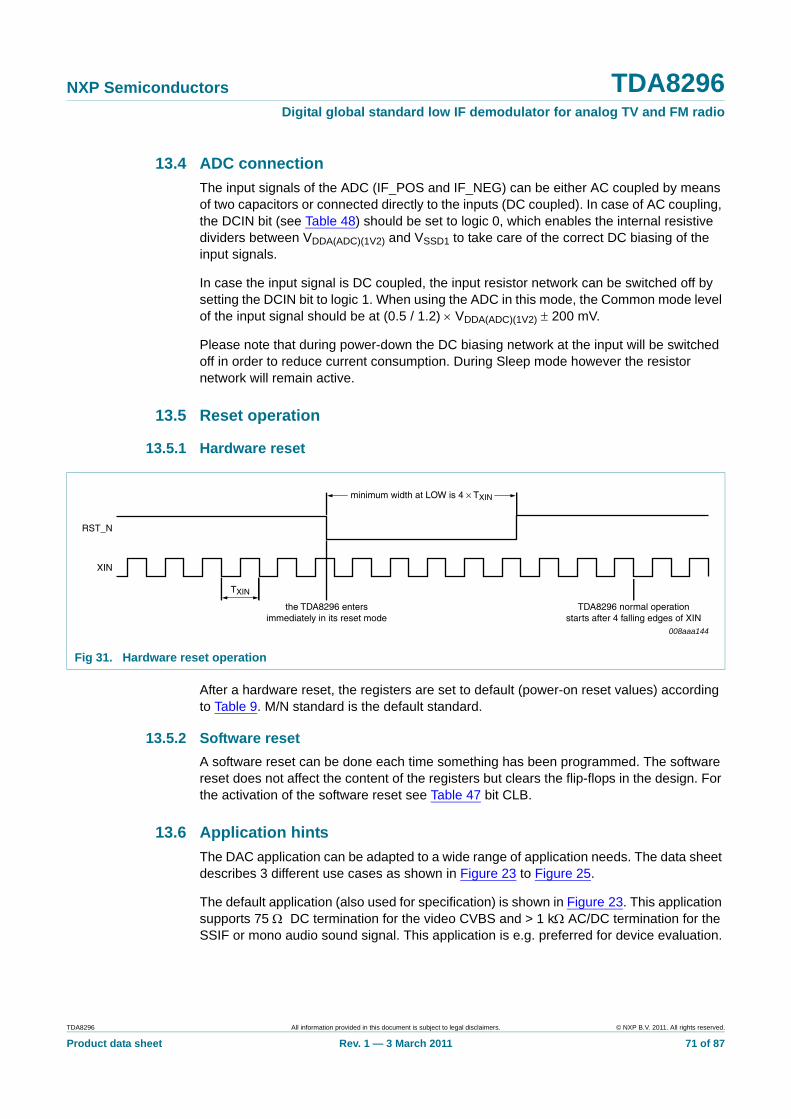
NXP Semiconductors TDA8296Digital global standard low IF demodulator for analog TV and FM radio
13.4 ADC connectionThe input signals of the ADC (IF_POS and IF_NEG) can be either AC coupled by means of two capacitors or connected directly to the inputs (DC coupled). In case of AC coupling, the DCIN bit (see Table 48) should be set to logic 0, which enables the internal resistive dividers between VDDA(ADC)(1V2) and VSSD1 to take care of the correct DC biasing of the input signals.
In case the input signal is DC coupled, the input resistor network can be switched off by setting the DCIN bit to logic 1. When using the ADC in this mode, the Common mode level of the input signal should be at (0.5 / 1.2) × VDDA(ADC)(1V2) ± 200 mV.
Please note that during power-down the DC biasing network at the input will be switched off in order to reduce current consumption. During Sleep mode however the resistor network will remain active.
13.5 Reset operation
13.5.1 Hardware reset
After a hardware reset, the registers are set to default (power-on reset values) according to Table 9. M/N standard is the default standard.
13.5.2 Software resetA software reset can be done each time something has been programmed. The software reset does not affect the content of the registers but clears the flip-flops in the design. For the activation of the software reset see Table 47 bit CLB.
13.6 Application hintsThe DAC application can be adapted to a wide range of application needs. The data sheet describes 3 different use cases as shown in Figure 23 to Figure 25.
The default application (also used for specification) is shown in Figure 23. This application supports 75 Ω DC termination for the video CVBS and > 1 kΩ AC/DC termination for the SSIF or mono audio sound signal. This application is e.g. preferred for device evaluation.
Fig 31. Hardware reset operation
008aaa144
TDA8296 normal operationstarts after 4 falling edges of XIN
the TDA8296 entersimmediately in its reset mode
TXIN
minimum width at LOW is 4 × TXIN
RST_N
XIN
TDA8296 All information provided in this document is subject to legal disclaimers. © NXP B.V. 2011. All rights reserved.
Product data sheet Rev. 1 — 3 March 2011 71 of 87
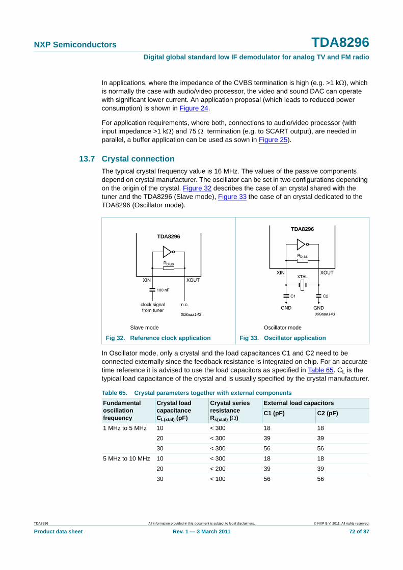
NXP Semiconductors TDA8296Digital global standard low IF demodulator for analog TV and FM radio
In applications, where the impedance of the CVBS termination is high (e.g. >1 kΩ), which is normally the case with audio/video processor, the video and sound DAC can operate with significant lower current. An application proposal (which leads to reduced power consumption) is shown in Figure 24.
For application requirements, where both, connections to audio/video processor (with input impedance >1 kΩ) and 75 Ω termination (e.g. to SCART output), are needed in parallel, a buffer application can be used as sown in Figure 25).
13.7 Crystal connectionThe typical crystal frequency value is 16 MHz. The values of the passive components depend on crystal manufacturer. The oscillator can be set in two configurations depending on the origin of the crystal. Figure 32 describes the case of an crystal shared with the tuner and the TDA8296 (Slave mode), Figure 33 the case of an crystal dedicated to the TDA8296 (Oscillator mode).
In Oscillator mode, only a crystal and the load capacitances C1 and C2 need to be connected externally since the feedback resistance is integrated on chip. For an accurate time reference it is advised to use the load capacitors as specified in Table 65. CL is the typical load capacitance of the crystal and is usually specified by the crystal manufacturer.
Slave mode Oscillator mode
Fig 32. Reference clock application Fig 33. Oscillator application
Table 65. Crystal parameters together with external components Fundamental oscillation frequency
Crystal load capacitance CL(xtal) (pF)
Crystal series resistance Rs(xtal) (Ω)
External load capacitorsC1 (pF) C2 (pF)
1 MHz to 5 MHz 10 < 300 18 18
20 < 300 39 39
30 < 300 56 56
5 MHz to 10 MHz 10 < 300 18 18
20 < 200 39 39
30 < 100 56 56
008aaa142
XOUTXIN
n.c.clock signalfrom tuner
Rbias
100 nF
TDA8296
008aaa143
XOUTXIN
GND GND
Rbias
C1 C2
XTAL
TDA8296
TDA8296 All information provided in this document is subject to legal disclaimers. © NXP B.V. 2011. All rights reserved.
Product data sheet Rev. 1 — 3 March 2011 72 of 87

NXP Semiconductors TDA8296Digital global standard low IF demodulator for analog TV and FM radio
13.8 Alternative ADC sampling ratesIn combination with a tuner front-end an alternative ADC sampling rates could be necessary. Please refer to Table 66
The default register setting is adapted to 16 MHz reference frequency (either from crystal or external source) and a nominal fADC = 54 MHz. In case of crosstalk of clock related signals (e.g. n × 54 MHz) into the RF input of connected tuner circuit, the potential disturbance of the wanted TV channel can be avoided by switching to the alternative ADC clock frequencies of 50.75 MHz or 57.25 MHz.
10 MHz to 15 MHz
10 < 160 18 18
20 < 60 39 39
15 MHz to 20 MHz
10 < 80 18 18
Table 65. Crystal parameters together with external components …continued
Fundamental oscillation frequency
Crystal load capacitance CL(xtal) (pF)
Crystal series resistance Rs(xtal) (Ω)
External load capacitorsC1 (pF) C2 (pF)
Table 66. Alternative ADC clocksFrequenciesADC SR 50.75 MHz 54.00 MHz 57.25 MHz
Clock PLL 101.50 MHz 108.00 MHz 114.50 MHz
Xtal frequency 16.00 MHz 16.00 MHz 16.00 MHz
DividerM 203 27 229
N 16 2 16
P 2 2 2
RegistersRegister 2Bh 01h 01h 02h
Register 38h 23h 23h 23h
Register 3Eh 63h 63h 63h
Register 3Fh 01h 01h 01h
Register 40h CAh 1Ah E4h
Register 41h 1Eh 02h 1Eh
Register 41h 61h 61h 61h
TDA8296 All information provided in this document is subject to legal disclaimers. © NXP B.V. 2011. All rights reserved.
Product data sheet Rev. 1 — 3 March 2011 73 of 87
NXP Semiconductors TDA8296Digital global standard low IF demodulator for analog TV and FM radio
14. Test information
14.1 Boundary scan interface (“IEEE Std. 1149.1”)The TDA8296 implements a boundary scan architecture to allow access to, and control of, board test support features within integrated circuits through a TAP. The TAP controller is a synchronous state machine that controls the sequence of operations on the TAP circuitry when the TMS signal changes. All state transitions occur on the basis of the TMS value on the rising edge of TCK. The instruction register is a shift register based design. It decodes the test to be performed and/or the test data register to be accessed. The instructions are shifted into the register through the TDI and are latched as the current instruction at the completion of the shifting process. The TDA8296 boundary scan architecture includes: a TAP controller, a scannable instruction register and three scannable test data registers: a boundary scan register, a device ID register, and a bypass register.
The supported instructions are: EXTEST, IDCODE, SAMPLE, INTEST, CLAMP, HIGHZ and BYPASS.
The boundary scan register is composed of 16 cells (see Table 67). Each cell is associated either to an input pad, an output pad, a bidirectional pad or to the bidirectional or 3-state command itself. All cells are of ‘observe and control’ type.
The device ID register is a 32-bit identification register that is included in the scan register itself and contains the ID number. It is a fixed value that identifies the chip.
ID number structure is:
ID version [3:0] = 1hID part number [15:0] = 224ChID manufacturer [11:1] = 015hID mandatory [0] = 1hIDCODE [31:0] = 1224 C02Bh
When the boundary scan function is not used, please connect the four dedicated input pins (TRST_N, TCK, TDI and TMS) to GND.
TDA8296 All information provided in this document is subject to legal disclaimers. © NXP B.V. 2011. All rights reserved.
Product data sheet Rev. 1 — 3 March 2011 74 of 87
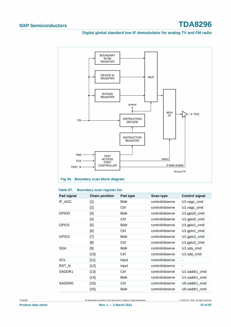
NXP Semiconductors TDA8296Digital global standard low IF demodulator for analog TV and FM radio
Fig 34. Boundary scan block diagram
Table 67. Boundary scan register list Pad signal Chain position Pad type Scan type Control signalIF_AGC [1] Bidir control/observe U1.vagc_cmd
[2] Ctrl control/observe U1.vagc_cmd
GPIO0 [3] Bidir control/observe U1.gpio0_cmd
[4] Ctrl control/observe U1.gpio0_cmd
GPIO1 [5] Bidir control/observe U1.gpio1_cmd
[6] Ctrl control/observe U1.gpio1_cmd
GPIO2 [7] Bidir control/observe U1.gpio2_cmd
[8] Ctrl control/observe U1.gpio2_cmd
SDA [9] Bidir control/observe U1.sda_cmd
[10] Ctrl control/observe U1.sda_cmd
SCL [11] input control/observe -
RST_N [12] input control/observe -
SADDR1 [13] Ctrl control/observe U1.saddr1_cmd
[14] Bidir control/observe U1.saddr1_cmd
SADDR0 [15] Ctrl control/observe U0.saddr1_cmd
[16] Bidir control/observe U0.saddr1_cmd
001aac078
BOUNDARYSCAN
REGISTER
DEVICE IDREGISTER MUX
MUXFF
BYPASSREGISTER
INSTRUCTIONDECODE
INSTRUCTIONREGISTER
TESTACCESS
PORTCONTROLLER
control
TDO
TDI
TMS
TCK
TRST_N3-state enable
select
TDA8296 All information provided in this document is subject to legal disclaimers. © NXP B.V. 2011. All rights reserved.
Product data sheet Rev. 1 — 3 March 2011 75 of 87
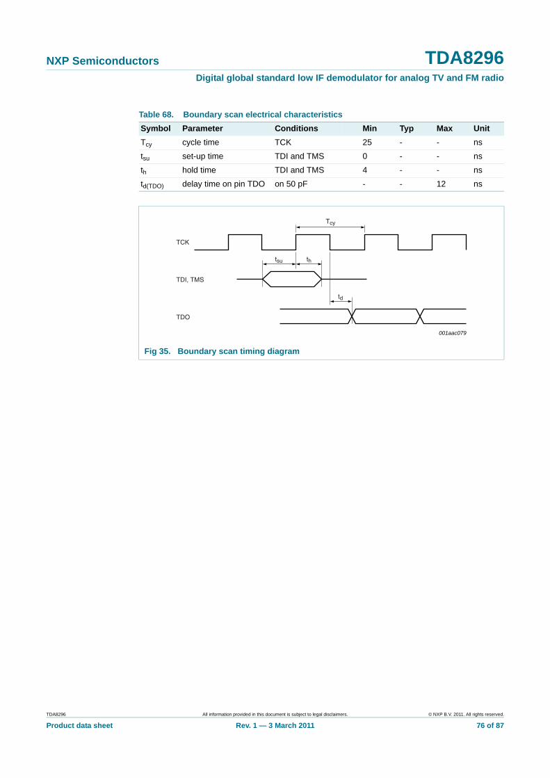
NXP Semiconductors TDA8296Digital global standard low IF demodulator for analog TV and FM radio
Table 68. Boundary scan electrical characteristics Symbol Parameter Conditions Min Typ Max UnitTcy cycle time TCK 25 - - ns
tsu set-up time TDI and TMS 0 - - ns
th hold time TDI and TMS 4 - - ns
td(TDO) delay time on pin TDO on 50 pF - - 12 ns
Fig 35. Boundary scan timing diagram
001aac079
Tcy
TCK
TDI, TMS
TDO
th
td
tsu
TDA8296 All information provided in this document is subject to legal disclaimers. © NXP B.V. 2011. All rights reserved.
Product data sheet Rev. 1 — 3 March 2011 76 of 87

NXP Semiconductors TDA8296Digital global standard low IF demodulator for analog TV and FM radio
15. Package outline
Fig 36. Package outline SOT618-1 (HVQFN40)
terminal 1index area
0.51
A1 EhbUNIT ye
0.2
c
REFERENCESOUTLINEVERSION
EUROPEANPROJECTION ISSUE DATE
IEC JEDEC JEITA
mm 6.15.9
Dh
4.253.95
y1
6.15.9
4.253.95
e1
4.5
e2
4.50.300.18
0.050.00
0.05 0.1
DIMENSIONS (mm are the original dimensions)
SOT618-1 MO-220- - - - - -
0.50.3
L
0.1
v
0.05
w
0 2.5 5 mm
scale
SOT618-1HVQFN40: plastic thermal enhanced very thin quad flat package; no leads;40 terminals; body 6 x 6 x 0.85 mm
A(1)
max.
AA1
c
detail X
yy1 Ce
L
Eh
Dh
e
e1
b11 20
40 31
30
2110
1
X
D
E
C
B A
e2
01-08-0802-10-22
terminal 1index area
1/2 e
1/2 e
ACC
Bv M
w M
Note
1. Plastic or metal protrusions of 0.075 mm maximum per side are not included.
D(1) E(1)
TDA8296 All information provided in this document is subject to legal disclaimers. © NXP B.V. 2011. All rights reserved.
Product data sheet Rev. 1 — 3 March 2011 77 of 87

NXP Semiconductors TDA8296Digital global standard low IF demodulator for analog TV and FM radio
16. Soldering of SMD packages
This text provides a very brief insight into a complex technology. A more in-depth account of soldering ICs can be found in Application Note AN10365 “Surface mount reflow soldering description”.
16.1 Introduction to solderingSoldering is one of the most common methods through which packages are attached to Printed Circuit Boards (PCBs), to form electrical circuits. The soldered joint provides both the mechanical and the electrical connection. There is no single soldering method that is ideal for all IC packages. Wave soldering is often preferred when through-hole and Surface Mount Devices (SMDs) are mixed on one printed wiring board; however, it is not suitable for fine pitch SMDs. Reflow soldering is ideal for the small pitches and high densities that come with increased miniaturization.
16.2 Wave and reflow solderingWave soldering is a joining technology in which the joints are made by solder coming from a standing wave of liquid solder. The wave soldering process is suitable for the following:
• Through-hole components• Leaded or leadless SMDs, which are glued to the surface of the printed circuit board
Not all SMDs can be wave soldered. Packages with solder balls, and some leadless packages which have solder lands underneath the body, cannot be wave soldered. Also, leaded SMDs with leads having a pitch smaller than ~0.6 mm cannot be wave soldered, due to an increased probability of bridging.
The reflow soldering process involves applying solder paste to a board, followed by component placement and exposure to a temperature profile. Leaded packages, packages with solder balls, and leadless packages are all reflow solderable.
Key characteristics in both wave and reflow soldering are:
• Board specifications, including the board finish, solder masks and vias• Package footprints, including solder thieves and orientation• The moisture sensitivity level of the packages• Package placement• Inspection and repair• Lead-free soldering versus SnPb soldering
16.3 Wave solderingKey characteristics in wave soldering are:
• Process issues, such as application of adhesive and flux, clinching of leads, board transport, the solder wave parameters, and the time during which components are exposed to the wave
• Solder bath specifications, including temperature and impurities
TDA8296 All information provided in this document is subject to legal disclaimers. © NXP B.V. 2011. All rights reserved.
Product data sheet Rev. 1 — 3 March 2011 78 of 87

NXP Semiconductors TDA8296Digital global standard low IF demodulator for analog TV and FM radio
16.4 Reflow solderingKey characteristics in reflow soldering are:
• Lead-free versus SnPb soldering; note that a lead-free reflow process usually leads to higher minimum peak temperatures (see Figure 37) than a SnPb process, thus reducing the process window
• Solder paste printing issues including smearing, release, and adjusting the process window for a mix of large and small components on one board
• Reflow temperature profile; this profile includes preheat, reflow (in which the board is heated to the peak temperature) and cooling down. It is imperative that the peak temperature is high enough for the solder to make reliable solder joints (a solder paste characteristic). In addition, the peak temperature must be low enough that the packages and/or boards are not damaged. The peak temperature of the package depends on package thickness and volume and is classified in accordance with Table 69 and 70
Moisture sensitivity precautions, as indicated on the packing, must be respected at all times.
Studies have shown that small packages reach higher temperatures during reflow soldering, see Figure 37.
Table 69. SnPb eutectic process (from J-STD-020C) Package thickness (mm) Package reflow temperature (°C)
Volume (mm3)< 350 ≥ 350
< 2.5 235 220
≥ 2.5 220 220
Table 70. Lead-free process (from J-STD-020C) Package thickness (mm) Package reflow temperature (°C)
Volume (mm3)< 350 350 to 2 000 > 2 000
< 1.6 260 260 260
1.6 to 2.5 260 250 245
> 2.5 250 245 245
TDA8296 All information provided in this document is subject to legal disclaimers. © NXP B.V. 2011. All rights reserved.
Product data sheet Rev. 1 — 3 March 2011 79 of 87
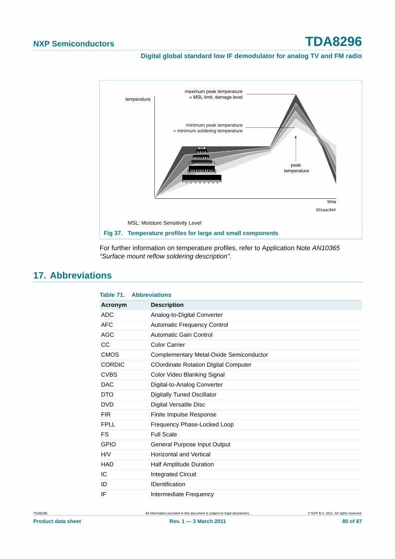
NXP Semiconductors TDA8296Digital global standard low IF demodulator for analog TV and FM radio
For further information on temperature profiles, refer to Application Note AN10365 “Surface mount reflow soldering description”.
17. Abbreviations
MSL: Moisture Sensitivity Level
Fig 37. Temperature profiles for large and small components
001aac844
temperature
time
minimum peak temperature= minimum soldering temperature
maximum peak temperature= MSL limit, damage level
peak temperature
Table 71. Abbreviations Acronym DescriptionADC Analog-to-Digital Converter
AFC Automatic Frequency Control
AGC Automatic Gain Control
CC Color Carrier
CMOS Complementary Metal-Oxide Semiconductor
CORDIC COordinate Rotation DIgital Computer
CVBS Color Video Blanking Signal
DAC Digital-to-Analog Converter
DTO Digitally Tuned Oscillator
DVD Digital Versatile Disc
FIR Finite Impulse Response
FPLL Frequency Phase-Locked Loop
FS Full Scale
GPIO General Purpose Input Output
H/V Horizontal and Vertical
HAD Half Amplitude Duration
IC Integrated Circuit
ID IDentification
IF Intermediate Frequency
TDA8296 All information provided in this document is subject to legal disclaimers. © NXP B.V. 2011. All rights reserved.
Product data sheet Rev. 1 — 3 March 2011 80 of 87
NXP Semiconductors TDA8296Digital global standard low IF demodulator for analog TV and FM radio
18. Revision history
NPC Neighbor Picture Carrier
NSC Neighbor Sound Carrier
PC Picture Carrier
PCB Printed-Circuit Board
PLL Phase-Locked Loop
POR Power-On Reset
PWM Pulse Width Modulation
QSS Quasi Split Sound
SAW Surface Acoustic Wave
SC Sound Carrier
SCART Syndicat des Constructeurs d'Appareils Radiorécepteurs et Téléviseurs Radio and Television Receiver Manufacturers' Association
SMD Surface Mounted Device
SSIF Second Sound Intermediate Frequency
TAP Test Access Port
VITS Vertical Interval Test Signal
Table 71. Abbreviations …continued
Acronym Description
Table 72. Revision history Document ID Release date Data sheet status Change notice SupersedesTDA8296 v.1 20110303 Product data sheet - -
TDA8296 All information provided in this document is subject to legal disclaimers. © NXP B.V. 2011. All rights reserved.
Product data sheet Rev. 1 — 3 March 2011 81 of 87

NXP Semiconductors TDA8296Digital global standard low IF demodulator for analog TV and FM radio
19. Legal information
19.1 Data sheet status
[1] Please consult the most recently issued document before initiating or completing a design.
[2] The term ‘short data sheet’ is explained in section “Definitions”.
[3] The product status of device(s) described in this document may have changed since this document was published and may differ in case of multiple devices. The latest product status information is available on the Internet at URL http://www.nxp.com.
19.2 DefinitionsDraft — The document is a draft version only. The content is still under internal review and subject to formal approval, which may result in modifications or additions. NXP Semiconductors does not give any representations or warranties as to the accuracy or completeness of information included herein and shall have no liability for the consequences of use of such information.
Short data sheet — A short data sheet is an extract from a full data sheet with the same product type number(s) and title. A short data sheet is intended for quick reference only and should not be relied upon to contain detailed and full information. For detailed and full information see the relevant full data sheet, which is available on request via the local NXP Semiconductors sales office. In case of any inconsistency or conflict with the short data sheet, the full data sheet shall prevail.
Product specification — The information and data provided in a Product data sheet shall define the specification of the product as agreed between NXP Semiconductors and its customer, unless NXP Semiconductors and customer have explicitly agreed otherwise in writing. In no event however, shall an agreement be valid in which the NXP Semiconductors product is deemed to offer functions and qualities beyond those described in the Product data sheet.
19.3 DisclaimersLimited warranty and liability — Information in this document is believed to be accurate and reliable. However, NXP Semiconductors does not give any representations or warranties, expressed or implied, as to the accuracy or completeness of such information and shall have no liability for the consequences of use of such information.
In no event shall NXP Semiconductors be liable for any indirect, incidental, punitive, special or consequential damages (including - without limitation - lost profits, lost savings, business interruption, costs related to the removal or replacement of any products or rework charges) whether or not such damages are based on tort (including negligence), warranty, breach of contract or any other legal theory.
Notwithstanding any damages that customer might incur for any reason whatsoever, NXP Semiconductors’ aggregate and cumulative liability towards customer for the products described herein shall be limited in accordance with the Terms and conditions of commercial sale of NXP Semiconductors.
Right to make changes — NXP Semiconductors reserves the right to make changes to information published in this document, including without limitation specifications and product descriptions, at any time and without notice. This document supersedes and replaces all information supplied prior to the publication hereof.
Suitability for use — NXP Semiconductors products are not designed, authorized or warranted to be suitable for use in life support, life-critical or safety-critical systems or equipment, nor in applications where failure or
malfunction of an NXP Semiconductors product can reasonably be expected to result in personal injury, death or severe property or environmental damage. NXP Semiconductors accepts no liability for inclusion and/or use of NXP Semiconductors products in such equipment or applications and therefore such inclusion and/or use is at the customer’s own risk.
Applications — Applications that are described herein for any of these products are for illustrative purposes only. NXP Semiconductors makes no representation or warranty that such applications will be suitable for the specified use without further testing or modification.
Customers are responsible for the design and operation of their applications and products using NXP Semiconductors products, and NXP Semiconductors accepts no liability for any assistance with applications or customer product design. It is customer’s sole responsibility to determine whether the NXP Semiconductors product is suitable and fit for the customer’s applications and products planned, as well as for the planned application and use of customer’s third party customer(s). Customers should provide appropriate design and operating safeguards to minimize the risks associated with their applications and products.
NXP Semiconductors does not accept any liability related to any default, damage, costs or problem which is based on any weakness or default in the customer’s applications or products, or the application or use by customer’s third party customer(s). Customer is responsible for doing all necessary testing for the customer’s applications and products using NXP Semiconductors products in order to avoid a default of the applications and the products or of the application or use by customer’s third party customer(s). NXP does not accept any liability in this respect.
Limiting values — Stress above one or more limiting values (as defined in the Absolute Maximum Ratings System of IEC 60134) will cause permanent damage to the device. Limiting values are stress ratings only and (proper) operation of the device at these or any other conditions above those given in the Recommended operating conditions section (if present) or the Characteristics sections of this document is not warranted. Constant or repeated exposure to limiting values will permanently and irreversibly affect the quality and reliability of the device.
Terms and conditions of commercial sale — NXP Semiconductors products are sold subject to the general terms and conditions of commercial sale, as published at http://www.nxp.com/profile/terms, unless otherwise agreed in a valid written individual agreement. In case an individual agreement is concluded only the terms and conditions of the respective agreement shall apply. NXP Semiconductors hereby expressly objects to applying the customer’s general terms and conditions with regard to the purchase of NXP Semiconductors products by customer.
No offer to sell or license — Nothing in this document may be interpreted or construed as an offer to sell products that is open for acceptance or the grant, conveyance or implication of any license under any copyrights, patents or other industrial or intellectual property rights.
Export control — This document as well as the item(s) described herein may be subject to export control regulations. Export might require a prior authorization from national authorities.
Document status[1][2] Product status[3] Definition
Objective [short] data sheet Development This document contains data from the objective specification for product development.
Preliminary [short] data sheet Qualification This document contains data from the preliminary specification.
Product [short] data sheet Production This document contains the product specification.
TDA8296 All information provided in this document is subject to legal disclaimers. © NXP B.V. 2011. All rights reserved.
Product data sheet Rev. 1 — 3 March 2011 82 of 87

NXP Semiconductors TDA8296Digital global standard low IF demodulator for analog TV and FM radio
Quick reference data — The Quick reference data is an extract of the product data given in the Limiting values and Characteristics sections of this document, and as such is not complete, exhaustive or legally binding.
Non-automotive qualified products — Unless this data sheet expressly states that this specific NXP Semiconductors product is automotive qualified, the product is not suitable for automotive use. It is neither qualified nor tested in accordance with automotive testing or application requirements. NXP Semiconductors accepts no liability for inclusion and/or use of non-automotive qualified products in automotive equipment or applications.
In the event that customer uses the product for design-in and use in automotive applications to automotive specifications and standards, customer (a) shall use the product without NXP Semiconductors’ warranty of the product for such automotive applications, use and specifications, and (b) whenever customer uses the product for automotive applications beyond
NXP Semiconductors’ specifications such use shall be solely at customer’s own risk, and (c) customer fully indemnifies NXP Semiconductors for any liability, damages or failed product claims resulting from customer design and use of the product for automotive applications beyond NXP Semiconductors’ standard warranty and NXP Semiconductors’ product specifications.
19.4 TrademarksNotice: All referenced brands, product names, service names and trademarks are the property of their respective owners.
I2C-bus — logo is a trademark of NXP B.V.
Silicon Tuner — is a trademark of NXP B.V.
20. Contact information
For more information, please visit: http://www.nxp.com
For sales office addresses, please send an email to: [email protected]
TDA8296 All information provided in this document is subject to legal disclaimers. © NXP B.V. 2011. All rights reserved.
Product data sheet Rev. 1 — 3 March 2011 83 of 87

NXP Semiconductors TDA8296Digital global standard low IF demodulator for analog TV and FM radio
21. Tables
Table 1. Quick reference data . . . . . . . . . . . . . . . . . . . . .3Table 2. Ordering information . . . . . . . . . . . . . . . . . . . . .5Table 3. Pin allocation table . . . . . . . . . . . . . . . . . . . . . . .7Table 4. Pin description . . . . . . . . . . . . . . . . . . . . . . . . . .8Table 5. Pin type description . . . . . . . . . . . . . . . . . . . . .10Table 6. Address format . . . . . . . . . . . . . . . . . . . . . . . . .13Table 7. I2C-bus transfer description . . . . . . . . . . . . . . .13Table 8. I2C-bus transfer description . . . . . . . . . . . . . . .14Table 9. I2C-bus register reference . . . . . . . . . . . . . . . .15Table 10. I2C-bus registers . . . . . . . . . . . . . . . . . . . . . . .18Table 11. STANDARD register (address 00h)
bit description . . . . . . . . . . . . . . . . . . . . . . . . .23Table 12. EASY_PROG register (address 01h)
bit description . . . . . . . . . . . . . . . . . . . . . . . . .23Table 13. Easy programming values . . . . . . . . . . . . . . . .24Table 14. DIV_FUNC register (address 02h)
bit description . . . . . . . . . . . . . . . . . . . . . . . . .25Table 15. ADC_HEADR register (address 03h)
bit description . . . . . . . . . . . . . . . . . . . . . . . . .25Table 16. PC_PLL_FUNC register (address 04h)
bit description . . . . . . . . . . . . . . . . . . . . . . . . .26Table 17. DTO_PC_LOW, DTO_PC_MID and
DTO_PC_HIGH register (address 09h to 0Bh) bit description . . . . . . . .26
Table 18. Values of DTO_PC per TV standard at 54 MHz sampling frequency . . . . . . . . . . . . .27
Table 19. DTO_SC_LOW, DTO_SC_MID and DTO_SC_HIGH register (address 0Ch to 0Eh) bit description . . . . . . . . . . . . . . . . . . . . . . . . .27
Table 20. Values for SSIF mode at 54 MHz sampling frequency . . . . . . . . . . . . . . . . . . . . . . . . . . . . .28
Table 21. FILTERS_1 register (address 0Fh) bit description . . . . . . . . . . . . . . . . . . . . . . . . .28
Table 22. FILTERS_2 register (address 10h) bit description . . . . . . . . . . . . . . . . . . . . . . . . .30
Table 23. GRP_DELAY register (address 11h) bit description . . . . . . . . . . . . . . . . . . . . . . . . .31
Table 24. D_IF_AGC_SET_1 register (address 12h) bit description . . . . . . . . . . . . . . . . . . . . . . . . .32
Table 25. D_IF_AGC_SET_2 register (address 13h) bit description . . . . . . . . . . . . . . . . . . . . . . . . .32
Table 26. T_IF_AGC_SET register (address 15h) bit description . . . . . . . . . . . . . . . . . . . . . . . . .32
Table 27. T_IF_AGC_LIM register (address 16h) bit description . . . . . . . . . . . . . . . . . . . . . . . . .33
Table 28. T_IF_AGC_FORCE register (address 17h) bit description . . . . . . . . . . . . . . . . . . . . . . . . .33
Table 29. V_SYNC_DEL register (address 1Ch)
bit description . . . . . . . . . . . . . . . . . . . . . . . . . 34Table 30. CVBS_SET register (address 1Dh)
bit description . . . . . . . . . . . . . . . . . . . . . . . . . 34Table 31. CVBS_LEVEL register (address 1Eh)
bit description . . . . . . . . . . . . . . . . . . . . . . . . . 35Table 32. CVBS_EQ register (address 1Fh)
bit description . . . . . . . . . . . . . . . . . . . . . . . . . 35Table 33. SSIF_MUTE register (address 05h)
bit description . . . . . . . . . . . . . . . . . . . . . . . . . 36Table 34. SOUNDSET_1 register (address 20h)
bit description . . . . . . . . . . . . . . . . . . . . . . . . . 36Table 35. SOUNDSET_2 register (address 21h)
bit description . . . . . . . . . . . . . . . . . . . . . . . . . 37Table 36. SOUND_LEVEL register (address 22h)
bit description . . . . . . . . . . . . . . . . . . . . . . . . . 38Table 37. SSIF_LEVEL register (address 23h)
bit description . . . . . . . . . . . . . . . . . . . . . . . . . 39Table 38. ADC_SAT register (address 24h)
bit description . . . . . . . . . . . . . . . . . . . . . . . . . 40Table 39. AFC register (address 25h) bit description . . . 41Table 40. Calculation of frequency deviation from AFC
value . . . . . . . . . . . . . . . . . . . . . . . . . . . . . . . . 41Table 41. HVPLL_STAT register (address 26h)
bit description . . . . . . . . . . . . . . . . . . . . . . . . . 42Table 42. D_IF_AGC_STAT register (address 27h)
bit description . . . . . . . . . . . . . . . . . . . . . . . . . 43Table 43. T_IF_AGC_STAT register (address 28h)
bit description . . . . . . . . . . . . . . . . . . . . . . . . . 43Table 44. ALT_FILT_COEF register (address 2Bh)
bit description . . . . . . . . . . . . . . . . . . . . . . . . . 43Table 45. SSIF_AGC_STAT register (address 2Dh)
bit description . . . . . . . . . . . . . . . . . . . . . . . . . 43Table 46. IDENTITY register (address 2Fh)
bit description . . . . . . . . . . . . . . . . . . . . . . . . . 43Table 47. CLB_STDBY register (address 30h)
bit description . . . . . . . . . . . . . . . . . . . . . . . . . 43Table 48. ADC_CTL register (address 33h)
bit description . . . . . . . . . . . . . . . . . . . . . . . . . 44Table 49. ADC_CTL_2 register (address 34h)
bit description . . . . . . . . . . . . . . . . . . . . . . . . . 44Table 50. VIDEODAC_CTL register (address 35h)
bit description . . . . . . . . . . . . . . . . . . . . . . . . . 45Table 51. AUDIODAC_CTL register (address 36h)
bit description . . . . . . . . . . . . . . . . . . . . . . . . . 46Table 52. DAC_REF_CLK_CTL register
(address 37h) bit description . . . . . . . . . . . . . . 46Table 53. PLL_REG07, PLL_REG08, PLL_REG09
and PLL_REG10 register (address 3Fh to 42h)
TDA8296 All information provided in this document is subject to legal disclaimers. © NXP B.V. 2011. All rights reserved.
Product data sheet Rev. 1 — 3 March 2011 84 of 87
continued >>
NXP Semiconductors TDA8296Digital global standard low IF demodulator for analog TV and FM radio
bit description . . . . . . . . . . . . . . . . . . . . . . . . .46Table 54. GPIOREG_0 register (address 44h)
bit description . . . . . . . . . . . . . . . . . . . . . . . . .47Table 55. GPIOREG_1 register (address 45h)
bit description . . . . . . . . . . . . . . . . . . . . . . . . .47Table 56. HVPLL signal configuration . . . . . . . . . . . . . . .48Table 57. GPIOREG_2 register (address 46h)
bit description . . . . . . . . . . . . . . . . . . . . . . . . .48Table 58. GD_EQ_SECTx_C1 and GD_EQ_SECTx_C2
(x = 1 to 4) register (address 4Bh to 52h) bit description . . . . . . . . . . . . . . . . . . . . . . . . . .49
Table 59. Coefficients used in group delay equalizer example . . . . . . . . . . . . . . . . . . . . . . . . . . . . . .50
Table 60. CVBS_EQ_COEFx_LOW and CVBS_EQ_COEFx_HIGH (x = 0 to 5) register (address 57h to 62h) bit description . . . . . . . .50
Table 61. Coefficients used in video equalizer example . . . . . . . . . . . . . . . . . . . . . . . . . . . . . .52
Table 62. Limiting values . . . . . . . . . . . . . . . . . . . . . . . . .53Table 63. Thermal characteristics . . . . . . . . . . . . . . . . . .53Table 64. Characteristics . . . . . . . . . . . . . . . . . . . . . . . . .54Table 65. Crystal parameters together with external
components . . . . . . . . . . . . . . . . . . . . . . . . . . .72Table 66. Alternative ADC clocks . . . . . . . . . . . . . . . . . . .73Table 67. Boundary scan register list . . . . . . . . . . . . . . .75Table 68. Boundary scan electrical characteristics . . . . .76Table 69. SnPb eutectic process (from J-STD-020C) . . .79Table 70. Lead-free process (from J-STD-020C) . . . . . .79Table 71. Abbreviations . . . . . . . . . . . . . . . . . . . . . . . . . .80Table 72. Revision history . . . . . . . . . . . . . . . . . . . . . . . .81
TDA8296 All information provided in this document is subject to legal disclaimers. © NXP B.V. 2011. All rights reserved.
Product data sheet Rev. 1 — 3 March 2011 85 of 87

NXP Semiconductors TDA8296Digital global standard low IF demodulator for analog TV and FM radio
22. Figures
Fig 1. Functional diagram of TDA8296 . . . . . . . . . . . . . .6Fig 2. Pin configuration for HVQFN40 . . . . . . . . . . . . . . .7Fig 3. I2C-bus Write mode . . . . . . . . . . . . . . . . . . . . . . .13Fig 4. Examples I2C-bus Write mode. . . . . . . . . . . . . . .13Fig 5. I2C-bus Read mode . . . . . . . . . . . . . . . . . . . . . . .14Fig 6. Example I2C-bus Read mode . . . . . . . . . . . . . . .14Fig 7. TDA8296 DTO_PC characteristic . . . . . . . . . . . .27Fig 8. TDA8296 DTO_SC characteristic . . . . . . . . . . . .28Fig 9. Video low-pass filters for sound carrier
suppression . . . . . . . . . . . . . . . . . . . . . . . . . . . . .29Fig 10. Notch filter for adjacent sound carrier
suppression . . . . . . . . . . . . . . . . . . . . . . . . . . . . .29Fig 11. Video low pass frequency response in
smooth roll off or low ripple mode . . . . . . . . . . . .30Fig 12. SSIF and FM radio band-pass filters
(center frequency 5.5 MHz chosen). . . . . . . . . . .31Fig 13. Video equalizer curves. . . . . . . . . . . . . . . . . . . . .36Fig 14. TDA8296 SSIF characteristic versus CS
(refer to Figure 23) typical values; termination 75 Ω and 1 kΩ in parallel . . . . . . . . . . . . . . . . . . .40
Fig 15. TDA8296 AFC characteristic . . . . . . . . . . . . . . . .42Fig 16. Internal low IF frequency response in front
of the VIF demodulator . . . . . . . . . . . . . . . . . . . .45Fig 17. Example for the programmable group delay
equalizer . . . . . . . . . . . . . . . . . . . . . . . . . . . . . . .50Fig 18. Example for the programmable video
equalizer . . . . . . . . . . . . . . . . . . . . . . . . . . . . . . .52Fig 19. Typical application of TDA8296 . . . . . . . . . . . . . .64Fig 20. IF input application for interlacing TDA1827x . . .64Fig 21. IF input application. . . . . . . . . . . . . . . . . . . . . . . .64Fig 22. Main application diagram. . . . . . . . . . . . . . . . . . .65Fig 23. 75 Ω load . . . . . . . . . . . . . . . . . . . . . . . . . . . . . . .66Fig 24. High ohmic load . . . . . . . . . . . . . . . . . . . . . . . . . .66Fig 25. Buffer application with 75 Ω load . . . . . . . . . . . . .67Fig 26. PCB pattern using circuit diagrams
of Figure 20, Figure 22, Figure 23 and 16 MHz reference from XTAL . . . . . . . . . . . . . . . . . . . . . .67
Fig 27. PCB pattern using circuit diagrams of Figure 20, Figure 22, Figure 23 and 16 MHz reference from master . . . . . . . . . . .68
Fig 28. TDA8296 calculated DAC characteristic . . . . . . .69Fig 29. Internal CVBS signal in front of video DAC
(typical characteristic) . . . . . . . . . . . . . . . . . . . . .70Fig 30. Internal SSIF signal in front of sound DAC
(typical characteristic, also dependent on SSIF_LVL[7:0] at address 23h) . . . . . . . . . . . . . .70
Fig 31. Hardware reset operation . . . . . . . . . . . . . . . . . .71Fig 32. Reference clock application. . . . . . . . . . . . . . . . .72Fig 33. Oscillator application . . . . . . . . . . . . . . . . . . . . . .72Fig 34. Boundary scan block diagram . . . . . . . . . . . . . . .75Fig 35. Boundary scan timing diagram . . . . . . . . . . . . . .76Fig 36. Package outline SOT618-1 (HVQFN40) . . . . . . .77Fig 37. Temperature profiles for large and small
components . . . . . . . . . . . . . . . . . . . . . . . . . . . . .80
TDA8296 All information provided in this document is subject to legal disclaimers. © NXP B.V. 2011. All rights reserved.
Product data sheet Rev. 1 — 3 March 2011 86 of 87
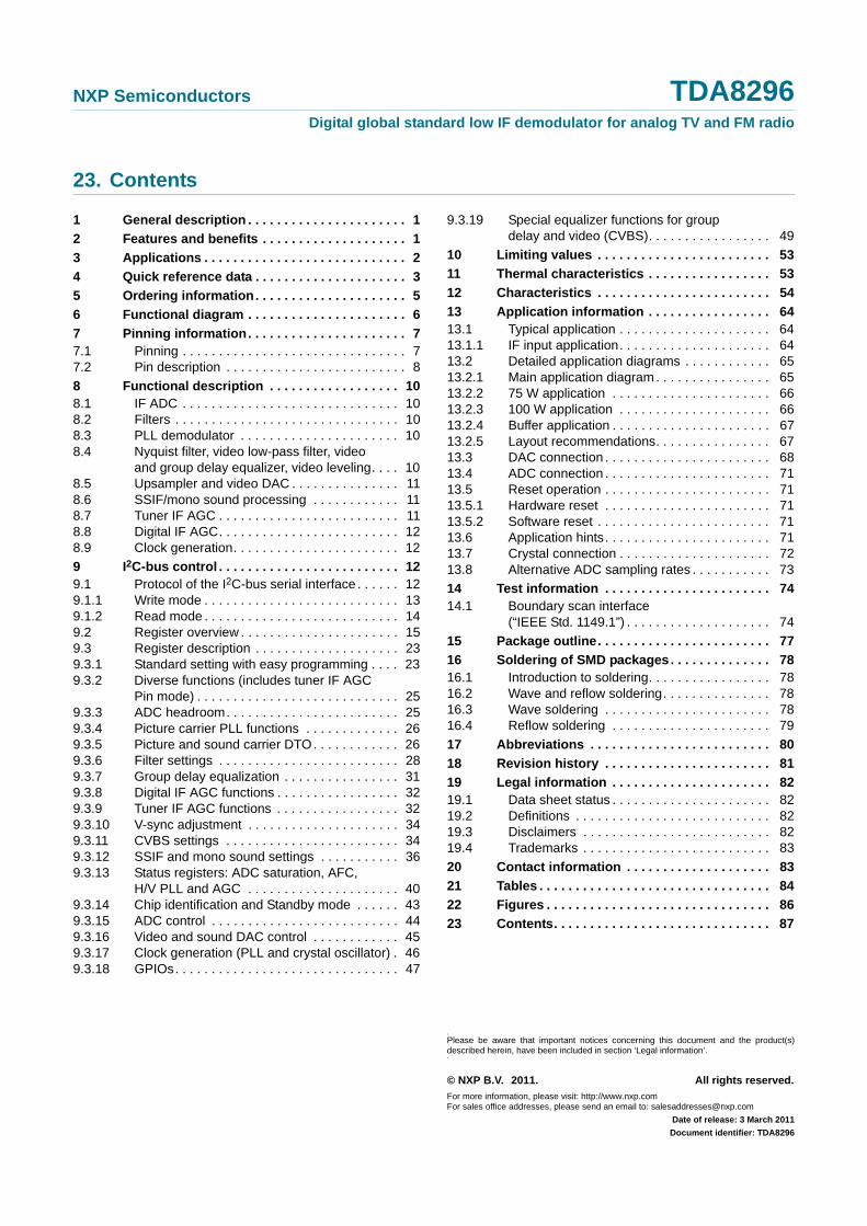
NXP Semiconductors TDA8296Digital global standard low IF demodulator for analog TV and FM radio
23. Contents
1 General description . . . . . . . . . . . . . . . . . . . . . . 12 Features and benefits . . . . . . . . . . . . . . . . . . . . 13 Applications . . . . . . . . . . . . . . . . . . . . . . . . . . . . 24 Quick reference data . . . . . . . . . . . . . . . . . . . . . 35 Ordering information. . . . . . . . . . . . . . . . . . . . . 56 Functional diagram . . . . . . . . . . . . . . . . . . . . . . 67 Pinning information. . . . . . . . . . . . . . . . . . . . . . 77.1 Pinning . . . . . . . . . . . . . . . . . . . . . . . . . . . . . . . 77.2 Pin description . . . . . . . . . . . . . . . . . . . . . . . . . 88 Functional description . . . . . . . . . . . . . . . . . . 108.1 IF ADC . . . . . . . . . . . . . . . . . . . . . . . . . . . . . . 108.2 Filters . . . . . . . . . . . . . . . . . . . . . . . . . . . . . . . 108.3 PLL demodulator . . . . . . . . . . . . . . . . . . . . . . 108.4 Nyquist filter, video low-pass filter, video
and group delay equalizer, video leveling. . . . 108.5 Upsampler and video DAC . . . . . . . . . . . . . . . 118.6 SSIF/mono sound processing . . . . . . . . . . . . 118.7 Tuner IF AGC . . . . . . . . . . . . . . . . . . . . . . . . . 118.8 Digital IF AGC. . . . . . . . . . . . . . . . . . . . . . . . . 128.9 Clock generation. . . . . . . . . . . . . . . . . . . . . . . 129 I2C-bus control . . . . . . . . . . . . . . . . . . . . . . . . . 129.1 Protocol of the I2C-bus serial interface . . . . . . 129.1.1 Write mode . . . . . . . . . . . . . . . . . . . . . . . . . . . 139.1.2 Read mode . . . . . . . . . . . . . . . . . . . . . . . . . . . 149.2 Register overview . . . . . . . . . . . . . . . . . . . . . . 159.3 Register description . . . . . . . . . . . . . . . . . . . . 239.3.1 Standard setting with easy programming . . . . 239.3.2 Diverse functions (includes tuner IF AGC
Pin mode) . . . . . . . . . . . . . . . . . . . . . . . . . . . . 259.3.3 ADC headroom. . . . . . . . . . . . . . . . . . . . . . . . 259.3.4 Picture carrier PLL functions . . . . . . . . . . . . . 269.3.5 Picture and sound carrier DTO. . . . . . . . . . . . 269.3.6 Filter settings . . . . . . . . . . . . . . . . . . . . . . . . . 289.3.7 Group delay equalization . . . . . . . . . . . . . . . . 319.3.8 Digital IF AGC functions . . . . . . . . . . . . . . . . . 329.3.9 Tuner IF AGC functions . . . . . . . . . . . . . . . . . 329.3.10 V-sync adjustment . . . . . . . . . . . . . . . . . . . . . 349.3.11 CVBS settings . . . . . . . . . . . . . . . . . . . . . . . . 349.3.12 SSIF and mono sound settings . . . . . . . . . . . 369.3.13 Status registers: ADC saturation, AFC,
H/V PLL and AGC . . . . . . . . . . . . . . . . . . . . . 409.3.14 Chip identification and Standby mode . . . . . . 439.3.15 ADC control . . . . . . . . . . . . . . . . . . . . . . . . . . 449.3.16 Video and sound DAC control . . . . . . . . . . . . 459.3.17 Clock generation (PLL and crystal oscillator) . 469.3.18 GPIOs. . . . . . . . . . . . . . . . . . . . . . . . . . . . . . . 47
9.3.19 Special equalizer functions for group delay and video (CVBS). . . . . . . . . . . . . . . . . 49
10 Limiting values . . . . . . . . . . . . . . . . . . . . . . . . 5311 Thermal characteristics . . . . . . . . . . . . . . . . . 5312 Characteristics . . . . . . . . . . . . . . . . . . . . . . . . 5413 Application information . . . . . . . . . . . . . . . . . 6413.1 Typical application . . . . . . . . . . . . . . . . . . . . . 6413.1.1 IF input application. . . . . . . . . . . . . . . . . . . . . 6413.2 Detailed application diagrams . . . . . . . . . . . . 6513.2.1 Main application diagram . . . . . . . . . . . . . . . . 6513.2.2 75 W application . . . . . . . . . . . . . . . . . . . . . . 6613.2.3 100 W application . . . . . . . . . . . . . . . . . . . . . 6613.2.4 Buffer application . . . . . . . . . . . . . . . . . . . . . . 6713.2.5 Layout recommendations. . . . . . . . . . . . . . . . 6713.3 DAC connection . . . . . . . . . . . . . . . . . . . . . . . 6813.4 ADC connection . . . . . . . . . . . . . . . . . . . . . . . 7113.5 Reset operation . . . . . . . . . . . . . . . . . . . . . . . 7113.5.1 Hardware reset . . . . . . . . . . . . . . . . . . . . . . . 7113.5.2 Software reset . . . . . . . . . . . . . . . . . . . . . . . . 7113.6 Application hints. . . . . . . . . . . . . . . . . . . . . . . 7113.7 Crystal connection . . . . . . . . . . . . . . . . . . . . . 7213.8 Alternative ADC sampling rates . . . . . . . . . . . 7314 Test information . . . . . . . . . . . . . . . . . . . . . . . 7414.1 Boundary scan interface
(“IEEE Std. 1149.1”) . . . . . . . . . . . . . . . . . . . . 7415 Package outline. . . . . . . . . . . . . . . . . . . . . . . . 7716 Soldering of SMD packages. . . . . . . . . . . . . . 7816.1 Introduction to soldering. . . . . . . . . . . . . . . . . 7816.2 Wave and reflow soldering. . . . . . . . . . . . . . . 7816.3 Wave soldering . . . . . . . . . . . . . . . . . . . . . . . 7816.4 Reflow soldering . . . . . . . . . . . . . . . . . . . . . . 7917 Abbreviations . . . . . . . . . . . . . . . . . . . . . . . . . 8018 Revision history . . . . . . . . . . . . . . . . . . . . . . . 8119 Legal information . . . . . . . . . . . . . . . . . . . . . . 8219.1 Data sheet status . . . . . . . . . . . . . . . . . . . . . . 8219.2 Definitions . . . . . . . . . . . . . . . . . . . . . . . . . . . 8219.3 Disclaimers . . . . . . . . . . . . . . . . . . . . . . . . . . 8219.4 Trademarks . . . . . . . . . . . . . . . . . . . . . . . . . . 8320 Contact information . . . . . . . . . . . . . . . . . . . . 8321 Tables . . . . . . . . . . . . . . . . . . . . . . . . . . . . . . . . 8422 Figures . . . . . . . . . . . . . . . . . . . . . . . . . . . . . . . 8623 Contents. . . . . . . . . . . . . . . . . . . . . . . . . . . . . . 87
© NXP B.V. 2011. All rights reserved.For more information, please visit: http://www.nxp.com For sales office addresses, please send an email to: [email protected]
Date of release: 3 March 2011Document identifier: TDA8296
Please be aware that important notices concerning this document and the product(s) described herein, have been included in section ‘Legal information’.