IF amplifier/demodulator for FM radio receivers Sheets/NXP PDFs/TDA1599.pdf · IF...
22
D A T A SH EET Product specification File under Integrated Circuits, IC01 May 1994 INTEGRATED CIRCUITS TDA1599 IF amplifier/demodulator for FM radio receivers
Transcript of IF amplifier/demodulator for FM radio receivers Sheets/NXP PDFs/TDA1599.pdf · IF...

DATA SHEET
Product specificationFile under Integrated Circuits, IC01
May 1994
INTEGRATED CIRCUITS
TDA1599IF amplifier/demodulator for FMradio receivers

May 1994 2
Philips Semiconductors Product specification
IF amplifier/demodulator for FM radioreceivers
TDA1599
FEATURES
• Balanced limiting amplifier
• Balanced coincidence demodulator
• Two open-collector stop pulse outputs formicrocomputer tuning control
• Simulated behaviour of a ratio detector (internal fieldstrength and detuning dependent voltage for dynamicAF signal muting)
• Mono/stereo blend field strength indication controlvoltage
• AFC output
• 3-state mode switch for FM-MUTE-ON, FM-MUTE-OFFand FM-OFF
• Internal compensation of AF signal total harmonicdistortion (THD)
• Built-in hum and ripple rejection circuits.
GENERAL DESCRIPTION
The TDA1599 provides IF amplification, symmetricalquadrature demodulation and level detection for qualityhome and car FM radio receivers and is suitable for monoand stereo reception. It may also be applied to commonfront ends, stereo decoders and AM receiver circuits.
QUICK REFERENCE DATA
All pin numbers mentioned in this data sheet refer to the SO-version (TDA1599T) unless otherwise specified.
ORDERING INFORMATION
Notes
1. SOT102-1; 1996 August 29.
2. SOT163-1; 1996 August 29.
SYMBOL PARAMETER MIN. TYP. MAX. UNIT
VP positive supply voltage (pin 1) 7.5 8.5 12 V
IP supply current (I2 = I7 = 0) − 20 26 mA
Vi IF input sensitivity for limiting on pin 20 (RMS value) 14 22 35 µV
Vo AF output signal on pin 4 (RMS value) 180 200 220 mV
S/N signal-to-noise ratio (fm = 400 Hz; ∆f = ±75 kHz) − 82 − dB
THD total harmonic distortion (fm = 1 kHz; ∆f = ±75 kHz) − 0.1 0.3 %
with K2 adjustment and FM-MUTE-OFF − 0.07 0.25 %
Tamb operating ambient temperature −40 − +85 °C
EXTENDEDTYPE NUMBER
PACKAGE
PINS PIN POSITION MATERIAL CODE
TDA1599 18 DIL plastic SOT102(1)
TDA1599T 20 mini-pack plastic SOT163A(2)

May 1994 3
Philips Semiconductors Product specification
IF amplifier/demodulator for FM radioreceivers
TDA1599
(1)
to c
onne
ct p
in 1
3 (1
1) to
gro
und
is o
nly
allo
wed
to m
easu
re th
e cu
rren
t on
pin
16 (
14)
(2)
FM
-MU
TE
-OF
F
(3)
FM
-OF
F
(4)
FM
-MU
TE
-ON
Fig
.1 B
lock
dia
gram
and
app
licat
ion
circ
uit (
TD
A15
99 p
inni
ng in
par
enth
esis
).

May 1994 4
Philips Semiconductors Product specification
IF amplifier/demodulator for FM radioreceivers
TDA1599
PINNING; note 1
Note
1. SO-version TDA1599T; pinning for DIL-version in parenthesis.
SYMBOL PIN DESCRIPTION
VP 1 (1) supply voltage (+8.5 V)
LVA 2 (2) level adjustment for stop condition
ULV 3 (3) unweighted level output / K2 adjustment
VoAF 4 (4) audio frequency output (MPX signal)
VREF 5 (5) reference voltage output
WLV 6 (6) weighted level output
MODE 7 (7) mode switch input
DDV 8 (8) detune detector voltage
n.c. 9 (−) not connected
DEMI1 10 (9) demodulator input 1
DEMI2 11 (10) demodulator input 2
n.c. 12 (−) not connected
TSW 13 (11) tau switch input
ST1 14 (12) STOP-1, stop pulse output 1
ST0 15 (13) STOP-0, stop pulse output 0
MUTE 16 (14) muting voltage
GND 17 (15) ground (0 V)
LFB1 18 (16) IF limiter feedback 1
LFB2 19 (17) IF limiter feedback 2
ViIF 20 (18) IF signal input
Fig.2 Pin configuration for DIL-version. Fig.3 Pin configuration for SO-version.
May 1994 5
Philips Semiconductors Product specification
IF amplifier/demodulator for FM radioreceivers
TDA1599
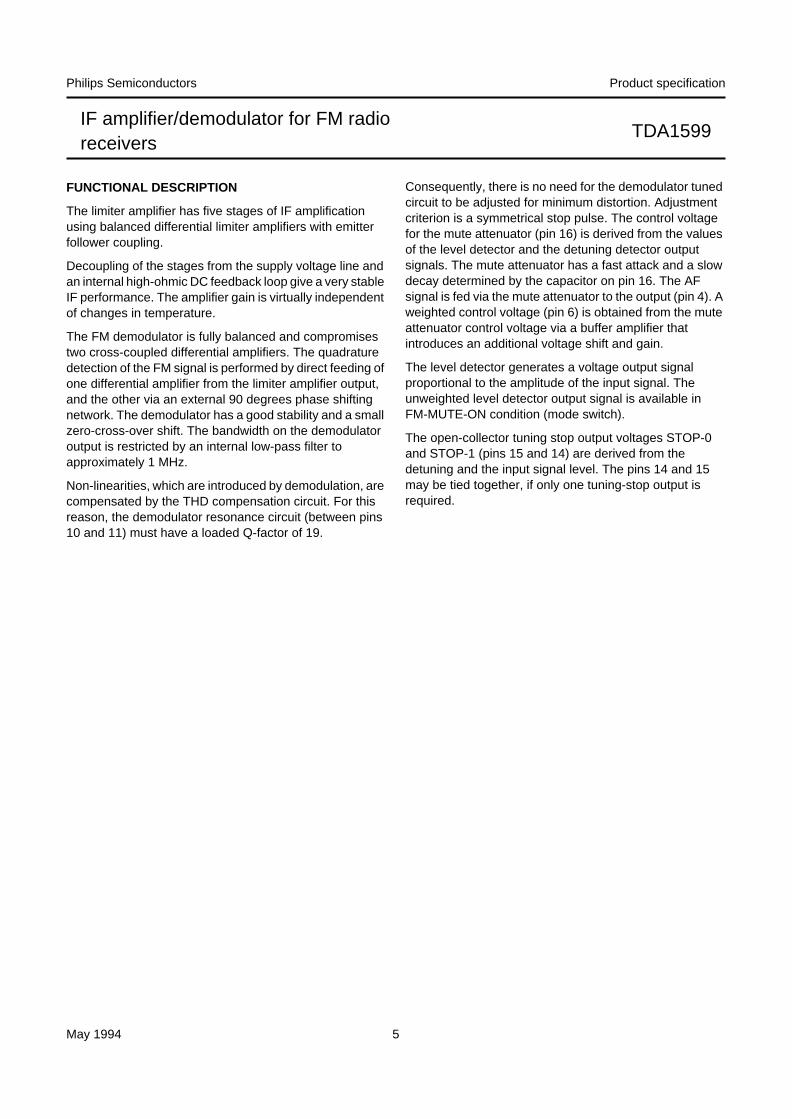
FUNCTIONAL DESCRIPTION
The limiter amplifier has five stages of IF amplificationusing balanced differential limiter amplifiers with emitterfollower coupling.
Decoupling of the stages from the supply voltage line andan internal high-ohmic DC feedback loop give a very stableIF performance. The amplifier gain is virtually independentof changes in temperature.
The FM demodulator is fully balanced and compromisestwo cross-coupled differential amplifiers. The quadraturedetection of the FM signal is performed by direct feeding ofone differential amplifier from the limiter amplifier output,and the other via an external 90 degrees phase shiftingnetwork. The demodulator has a good stability and a smallzero-cross-over shift. The bandwidth on the demodulatoroutput is restricted by an internal low-pass filter toapproximately 1 MHz.
Non-linearities, which are introduced by demodulation, arecompensated by the THD compensation circuit. For thisreason, the demodulator resonance circuit (between pins10 and 11) must have a loaded Q-factor of 19.
Consequently, there is no need for the demodulator tunedcircuit to be adjusted for minimum distortion. Adjustmentcriterion is a symmetrical stop pulse. The control voltagefor the mute attenuator (pin 16) is derived from the valuesof the level detector and the detuning detector outputsignals. The mute attenuator has a fast attack and a slowdecay determined by the capacitor on pin 16. The AFsignal is fed via the mute attenuator to the output (pin 4). Aweighted control voltage (pin 6) is obtained from the muteattenuator control voltage via a buffer amplifier thatintroduces an additional voltage shift and gain.
The level detector generates a voltage output signalproportional to the amplitude of the input signal. Theunweighted level detector output signal is available inFM-MUTE-ON condition (mode switch).
The open-collector tuning stop output voltages STOP-0and STOP-1 (pins 15 and 14) are derived from thedetuning and the input signal level. The pins 14 and 15may be tied together, if only one tuning-stop output isrequired.

May 1994 6
Philips Semiconductors Product specification
IF amplifier/demodulator for FM radioreceivers
TDA1599
LIMITING VALUES (TDA1599T PINNING)In accordance with the Absolute Maximum Rating System (IEC 134).
Note to the limiting values
1. Equivalent to discharging a 100 pF capacitor through a 1.5 kΩ series resistor.
THERMAL RESISTANCE
SYMBOL PARAMETER MIN. MAX. UNIT
VP supply voltage (pin 1) −0.3 +13 V
Vn1 voltage at pins 2, 4, 5, 6, 10, 11 and 16 −0.3 +10 V
Vn2 voltage at pins 7, 3, 8, 14, 15, 18, 19 and 20 −0.3 VP V
V13 voltage on pin 13 − 6 V
I14, 15 current at pins 14 and 15 − 2 mA
Ptot total power dissipation − 360 mW
Tstg storage temperature −55 +150 °CTamb operating ambient temperature −40 +85 °CVESD electrostatic handling; note 1
all pins except 5 and 7 − ±2000 V
pin 5 − +800 V
−2000 V
pin 7 − +1000 V
−2000 V
SYMBOL PARAMETER THERMAL RESISTANCE
Rth j-a from junction to ambient in free air
SOT102 80 K/W
SOT163A 90 K/W
May 1994 7
Philips Semiconductors Product specification
IF amplifier/demodulator for FM radioreceivers
TDA1599
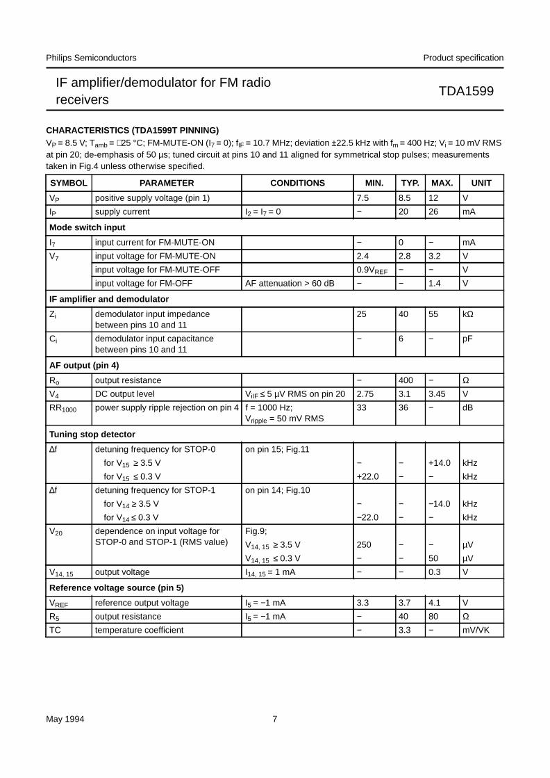
CHARACTERISTICS (TDA1599T PINNING)VP = 8.5 V; Tamb = +25 °C; FM-MUTE-ON (I7 = 0); fIF = 10.7 MHz; deviation ±22.5 kHz with fm = 400 Hz; Vi = 10 mV RMSat pin 20; de-emphasis of 50 µs; tuned circuit at pins 10 and 11 aligned for symmetrical stop pulses; measurementstaken in Fig.4 unless otherwise specified.
SYMBOL PARAMETER CONDITIONS MIN. TYP. MAX. UNIT
VP positive supply voltage (pin 1) 7.5 8.5 12 V
IP supply current I2 = I7 = 0 − 20 26 mA
Mode switch input
I7 input current for FM-MUTE-ON − 0 − mA
V7 input voltage for FM-MUTE-ON 2.4 2.8 3.2 V
input voltage for FM-MUTE-OFF 0.9VREF − − V
input voltage for FM-OFF AF attenuation > 60 dB − − 1.4 V
IF amplifier and demodulator
Zi demodulator input impedancebetween pins 10 and 11
25 40 55 kΩ
Ci demodulator input capacitancebetween pins 10 and 11
− 6 − pF
AF output (pin 4)
Ro output resistance − 400 − ΩV4 DC output level ViIF ≤ 5 µV RMS on pin 20 2.75 3.1 3.45 V
RR1000 power supply ripple rejection on pin 4 f = 1000 Hz;Vripple = 50 mV RMS
33 36 − dB
Tuning stop detector
∆f detuning frequency for STOP-0 on pin 15; Fig.11
for V15 ≥ 3.5 V − − +14.0 kHz
for V15 ≤ 0.3 V +22.0 − − kHz
∆f detuning frequency for STOP-1 on pin 14; Fig.10
for V14 ≥ 3.5 V − − −14.0 kHz
for V14 ≤ 0.3 V −22.0 − − kHz
V20 dependence on input voltage forSTOP-0 and STOP-1 (RMS value)
Fig.9;
V14, 15 ≥ 3.5 V 250 − − µV
V14, 15 ≤ 0.3 V − − 50 µV
V14, 15 output voltage I14, 15 = 1 mA − − 0.3 V
Reference voltage source (pin 5)
VREF reference output voltage I5 = −1 mA 3.3 3.7 4.1 V
R5 output resistance I5 = −1 mA − 40 80 ΩTC temperature coefficient − 3.3 − mV/VK

May 1994 8
Philips Semiconductors Product specification
IF amplifier/demodulator for FM radioreceivers
TDA1599
External muting
V16 muting voltage at I2 = 0 V20 ≤ 5 µV RMS; Fig.12 1.45 1.75 2.05 V
V20 = 1 mV RMS 3.0 3.45 3.9 V
S steepness of control voltage(slope: 100 µV ≤ V20 ≤ 100 mV)20 ∆log V20 = 20 dB (∆V16 / ∆log V20)
− 0.85 − V/dec
Internal mute α = 20 log ( ∆V4(FM-MUTE-OFF)/ ∆V4(FM-MUTE-ON))
α mute voltage V16 ≥ VREF − 0 − dB
V16 = 0.77VREF 1.5 − 4.5 dB
V16 = 0.55VREF − 20 − dB
I16 current for capacitor (pin 16)
charge current V13 = 0 V − −8 − µA
discharge current V13 = 0 V − +120 − µA
charge current V13 = VREF − −100 − µA
discharge current V13 = VREF − +120 − µA
Level detector
R6 output resistance − − 500 ΩV6 output voltage at I2 = 0 V20 ≤ 5 µV RMS; Fig.14 0.1 − 1.1 V
V20 = 1 mV RMS 3.0 − 4.2 V
±200 kHz detuning 1.2 1.5 1.8 V
output voltage at V2 = V5 V20 ≤ 5 µV RMS − − 0.3 V
∆V6 output voltage at detuning ±45 kHz detuning − − 0.2 V
TC temperature coefficient − 3.3 − mV/VK
∆f detuning frequency V6 = 1.8 V; Fig.13 90 − 160 kHz
S steepness of control voltage(slope: 50 µV ≤ V20 ≤ 50 mV)20 ∆log V20 = 20 dB (∆V6 / ∆log V20)
1.4 1.7 2.0 V/dec
∆V6/∆f slope of output voltage at detuning ∆f = 125 ± 20 kHz − 35 − mV/kHz
S level shift adjustments
range by pin 2 ±∆V6/VREF 0.42 0.5 − V/V
gain −∆V6/∆V2 − 1.7 − V/V
range by pin 2 ±∆V16/VREF 0.21 0.25 − V/V
gain −∆V16/∆V2 − 0.85 − V/V
SYMBOL PARAMETER CONDITIONS MIN. TYP. MAX. UNIT
May 1994 9
Philips Semiconductors Product specification
IF amplifier/demodulator for FM radioreceivers
TDA1599
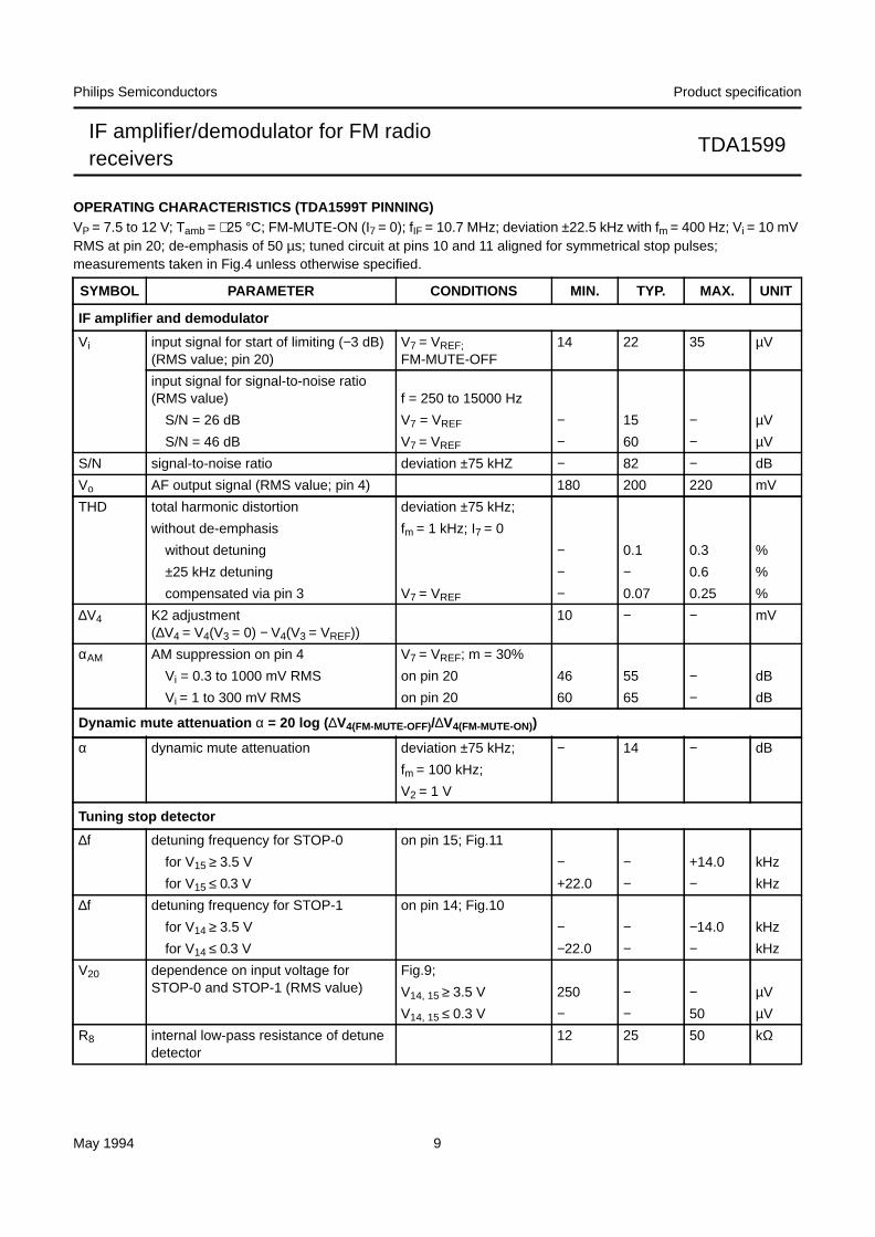
OPERATING CHARACTERISTICS (TDA1599T PINNING)VP = 7.5 to 12 V; Tamb = +25 °C; FM-MUTE-ON (I7 = 0); fIF = 10.7 MHz; deviation ±22.5 kHz with fm = 400 Hz; Vi = 10 mVRMS at pin 20; de-emphasis of 50 µs; tuned circuit at pins 10 and 11 aligned for symmetrical stop pulses;measurements taken in Fig.4 unless otherwise specified.
SYMBOL PARAMETER CONDITIONS MIN. TYP. MAX. UNIT
IF amplifier and demodulator
Vi input signal for start of limiting (−3 dB)(RMS value; pin 20)
V7 = VREF;FM-MUTE-OFF
14 22 35 µV
input signal for signal-to-noise ratio(RMS value) f = 250 to 15000 Hz
S/N = 26 dB V7 = VREF − 15 − µV
S/N = 46 dB V7 = VREF − 60 − µV
S/N signal-to-noise ratio deviation ±75 kHZ − 82 − dB
Vo AF output signal (RMS value; pin 4) 180 200 220 mV
THD total harmonic distortion deviation ±75 kHz;
without de-emphasis fm = 1 kHz; I7 = 0
without detuning − 0.1 0.3 %
±25 kHz detuning − − 0.6 %
compensated via pin 3 V7 = VREF − 0.07 0.25 %
∆V4 K2 adjustment(∆V4 = V4(V3 = 0) − V4(V3 = VREF))
10 − − mV
αAM AM suppression on pin 4 V7 = VREF; m = 30%
Vi = 0.3 to 1000 mV RMS on pin 20 46 55 − dB
Vi = 1 to 300 mV RMS on pin 20 60 65 − dB
Dynamic mute attenuation α = 20 log ( ∆V4(FM-MUTE-OFF)/∆V4(FM-MUTE-ON))
α dynamic mute attenuation deviation ±75 kHz; − 14 − dB
fm = 100 kHz;
V2 = 1 V
Tuning stop detector
∆f detuning frequency for STOP-0 on pin 15; Fig.11
for V15 ≥ 3.5 V − − +14.0 kHz
for V15 ≤ 0.3 V +22.0 − − kHz
∆f detuning frequency for STOP-1 on pin 14; Fig.10
for V14 ≥ 3.5 V − − −14.0 kHz
for V14 ≤ 0.3 V −22.0 − − kHz
V20 dependence on input voltage forSTOP-0 and STOP-1 (RMS value)
Fig.9;
V14, 15 ≥ 3.5 V 250 − − µV
V14, 15 ≤ 0.3 V − − 50 µV
R8 internal low-pass resistance of detunedetector
12 25 50 kΩ

May 1994 10
Philips Semiconductors Product specification
IF amplifier/demodulator for FM radioreceivers
TDA1599
V8 voltage on capacitor I7 = 0; − 2.2 − V
Vi ≤ 5 µV RMS on
input pin 20
Level detector (I 2 = 0)
V6 output voltage V20 ≤ 5 µV RMS 0.1 − 1.1 V
V20 = 1 mV RMS 3.0 − 4.2 V
Reference voltage source (pin 5)
VREF reference output voltage I5 = −1 mA 3.3 3.7 4.1 V
Operation with AM-IF
Level and stop information (on pins 6,13, 14, 15 and 16) is provided for the modes FM-MUTE-ON andFM-MUTE-OFF. This information is also available in the FM-OFF mode when an AM-IF signal is input (for example455 kHz). This can also provide a valid detuning information when a suitable AM-IF resonance circuit is provided fordemodulator (Fig.18).
SYMBOL PARAMETER CONDITIONS MIN. TYP. MAX. UNIT
Fig.4 Test circuit (TDA1599 pinning in parenthesis).
May 1994 11
Philips Semiconductors Product specification
IF amplifier/demodulator for FM radioreceivers
TDA1599
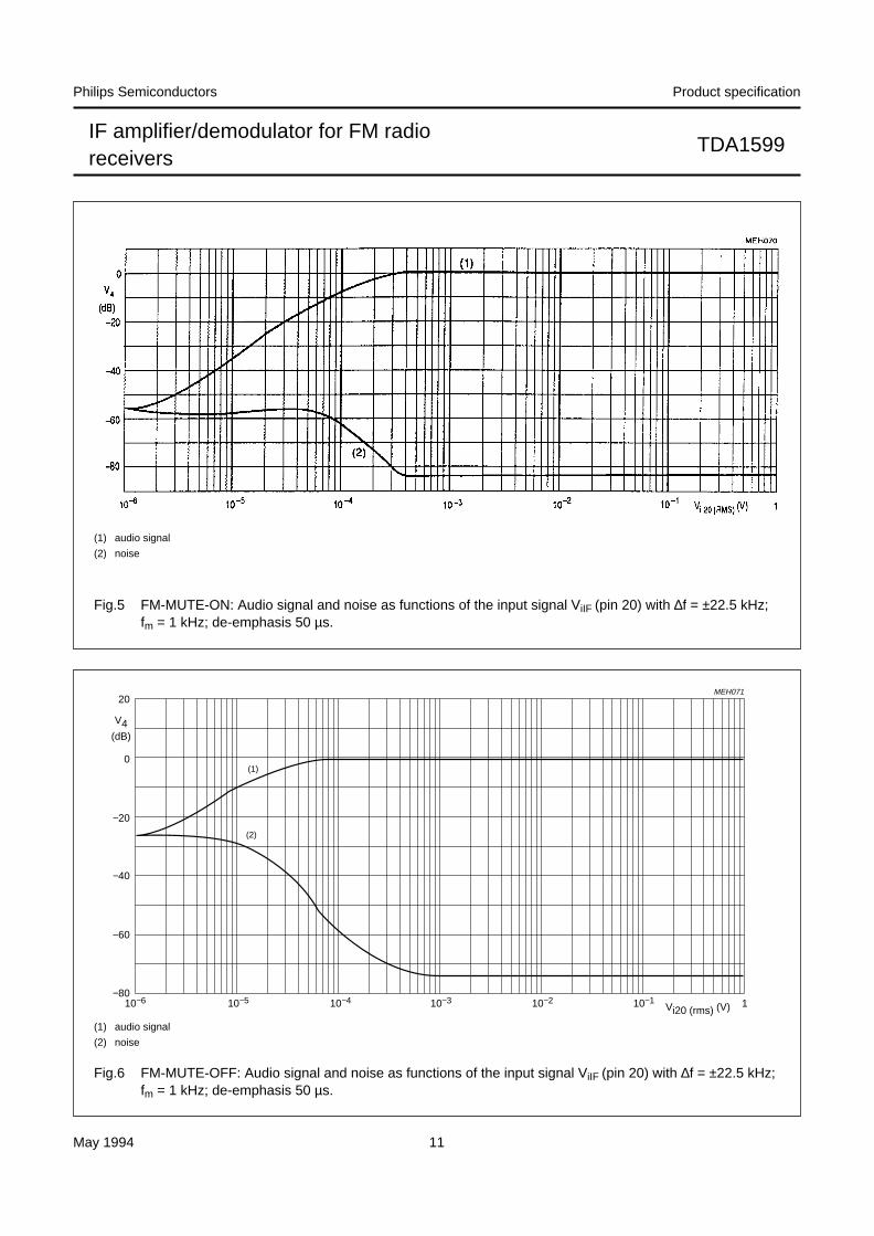
Fig.5 FM-MUTE-ON: Audio signal and noise as functions of the input signal ViIF (pin 20) with ∆f = ±22.5 kHz;fm = 1 kHz; de-emphasis 50 µs.
(1) audio signal
(2) noise
handbook, full pagewidth20
V4 (dB)
−20
−40
−60
−80
0
MEH071
10−6 10−5 10−4 10−3 10−2 10−1 1
(1)
(2)
Vi20 (rms) (V)
Fig.6 FM-MUTE-OFF: Audio signal and noise as functions of the input signal ViIF (pin 20) with ∆f = ±22.5 kHz;fm = 1 kHz; de-emphasis 50 µs.
(1) audio signal
(2) noise
May 1994 12
Philips Semiconductors Product specification
IF amplifier/demodulator for FM radioreceivers
TDA1599
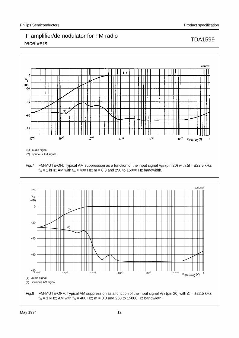
Fig.7 FM-MUTE-ON: Typical AM suppression as a function of the input signal ViIF (pin 20) with ∆f = ±22.5 kHz;fm = 1 kHz; AM with fm = 400 Hz; m = 0.3 and 250 to 15000 Hz bandwidth.
(1) audio signal
(2) spurious AM signal
handbook, full pagewidth20
V4 (dB)
−20
−40
−60
−80
0
MEH073
10−6 10−5 10−4 10−3 10−2 10−1 1
(1)
(2)
Vi20 (rms) (V)
Fig.8 FM-MUTE-OFF: Typical AM suppression as a function of the input signal ViIF (pin 20) with ∆f = ±22.5 kHz;fm = 1 kHz; AM with fm = 400 Hz; m = 0.3 and 250 to 15000 Hz bandwidth.
(1) audio signal
(2) spurious AM signal
May 1994 13
Philips Semiconductors Product specification
IF amplifier/demodulator for FM radioreceivers
TDA1599
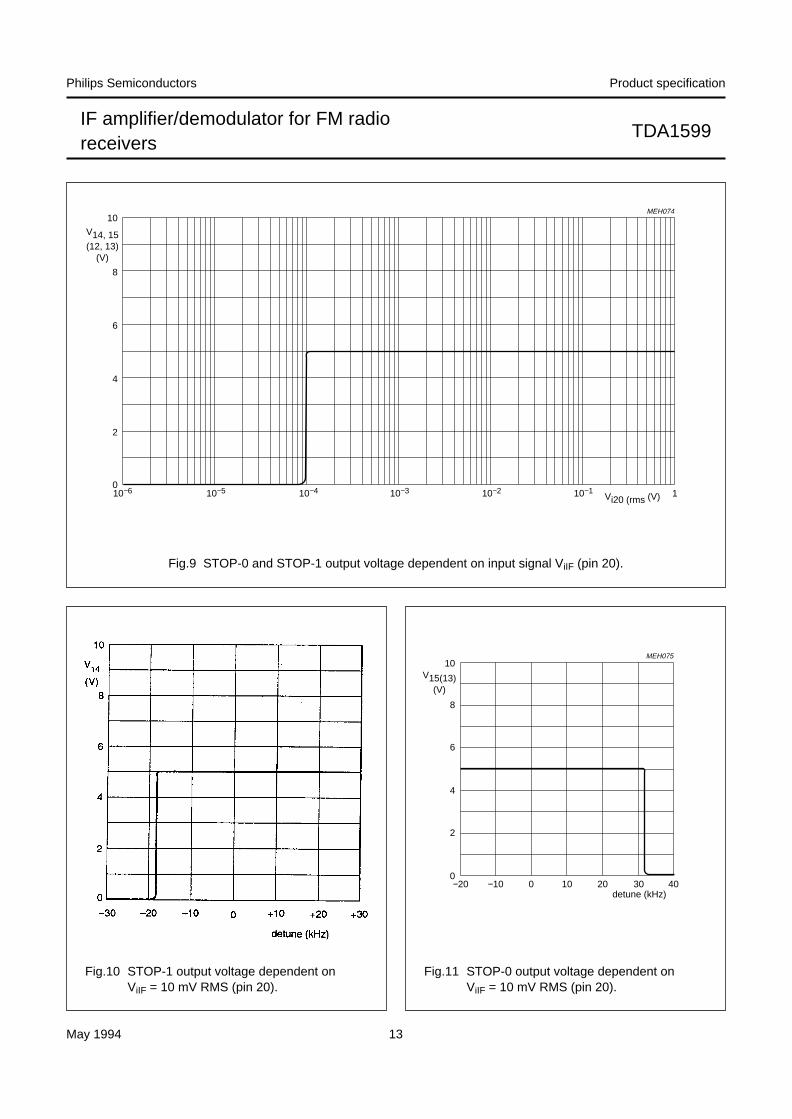
Fig.9 STOP-0 and STOP-1 output voltage dependent on input signal ViIF (pin 20).
handbook, full pagewidth10
V14, 15 (12, 13)
(V)
0
2
4
6
8
MEH074
10−6 10−5 10−4 10−3 10−2 10−1 1Vi20 (rms (V)
Fig.10 STOP-1 output voltage dependent onViIF = 10 mV RMS (pin 20).
Fig.11 STOP-0 output voltage dependent onViIF = 10 mV RMS (pin 20).
handbook, halfpage10
0
8
6
4
2
MEH075
detune (kHz)
V15(13) (V)
−20 −10 10 20 30 400
May 1994 14
Philips Semiconductors Product specification
IF amplifier/demodulator for FM radioreceivers
TDA1599
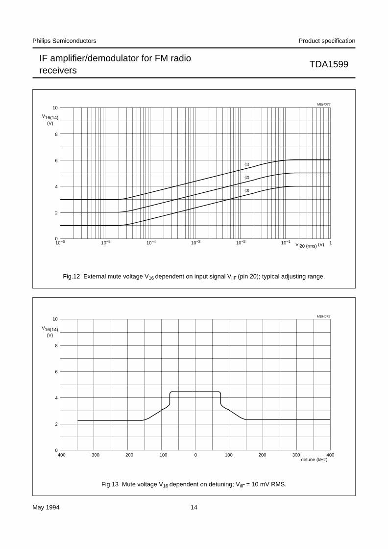
Fig.12 External mute voltage V16 dependent on input signal ViIF (pin 20); typical adjusting range.
handbook, full pagewidth10
V16(14) (V)
0
2
4
6
8
MEH076
10−6 10−5 10−4 10−3 10−2 10−1 1
(1)
(2)
(3)
Vi20 (rms) (V)
Fig.13 Mute voltage V16 dependent on detuning; ViIF = 10 mV RMS.
handbook, full pagewidth
detune (kHz)
10
0−400 −300
V16(14) (V)
−200 −100 1000 200 300 400
2
4
6
8
MEH079

May 1994 15
Philips Semiconductors Product specification
IF amplifier/demodulator for FM radioreceivers
TDA1599
Fig.14 Control voltage V6 dependent on input signal ViIF (pin 20); typical adjusting range.
Fig.15 Control voltage V6 dependent on detuning; ViIF = 10 mV RMS.
handbook, full pagewidth
detune (kHz)
10
0−400 −300
V6 (V)
−200 −100 1000 200 300 400
2
4
6
8
MED834
May 1994 16
Philips Semiconductors Product specification
IF amplifier/demodulator for FM radioreceivers
TDA1599
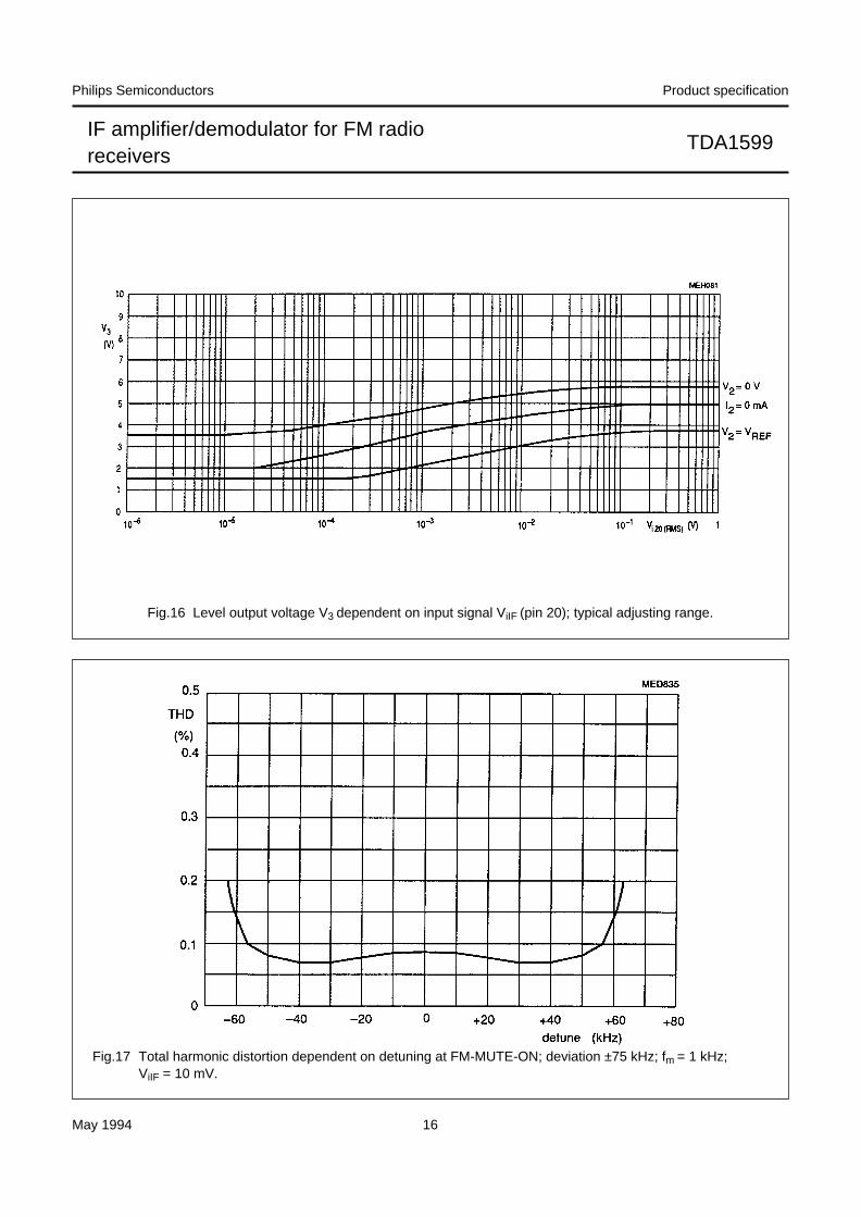
Fig.16 Level output voltage V3 dependent on input signal ViIF (pin 20); typical adjusting range.
Fig.17 Total harmonic distortion dependent on detuning at FM-MUTE-ON; deviation ±75 kHz; fm = 1 kHz;ViIF = 10 mV.

May 1994 17
Philips Semiconductors Product specification
IF amplifier/demodulator for FM radioreceivers
TDA1599
Fig.18 Interface for AM stop pulse application (SO-version).
May 1994 18
Philips Semiconductors Product specification
IF amplifier/demodulator for FM radioreceivers
TDA1599
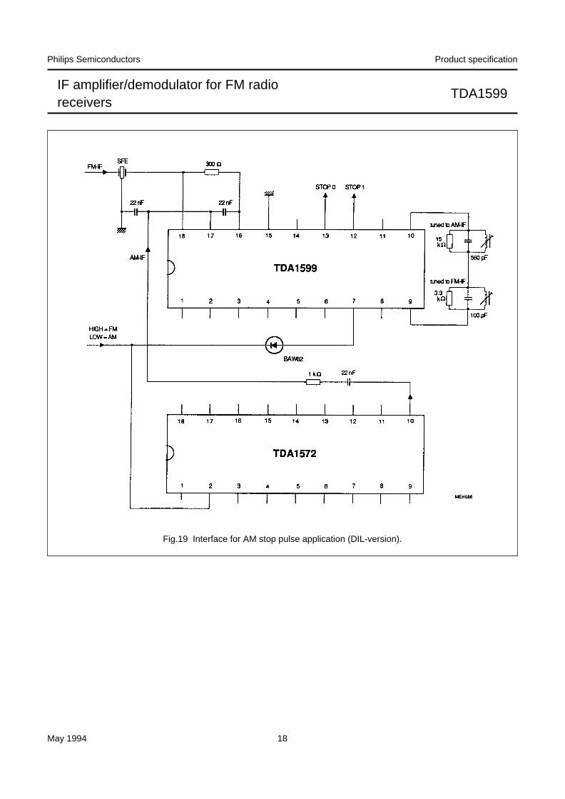
Fig.19 Interface for AM stop pulse application (DIL-version).
May 1994 19
Philips Semiconductors Product specification
IF amplifier/demodulator for FM radioreceivers
TDA1599
PACKAGE OUTLINES
REFERENCESOUTLINEVERSION
EUROPEANPROJECTION ISSUE DATE
IEC JEDEC EIAJ
SOT102-193-10-1495-01-23
UNIT Amax.
1 2 b1(1) (1) (1)
b2 c D E e M ZHL
mm
DIMENSIONS (inch dimensions are derived from the original mm dimensions)
A min.
A max. b
max.wMEe1
1.401.14
0.530.38
0.320.23
21.821.4
6.486.20
3.93.4 0.2542.54 7.62
8.257.80
9.58.3 0.854.7 0.51 3.7
inches 0.0550.044
0.0210.015
0.0130.009
1.401.14
0.0550.044
0.860.84
0.260.24
0.150.13 0.010.10 0.30
0.320.31
0.370.33 0.0330.19 0.020 0.15
MH
c
(e )1
ME
A
L
seat
ing
plan
e
A1
w Mb1
b2
e
D
A2
Z
18
1
10
9
b
E
pin 1 index
0 5 10 mm
scale
Note
1. Plastic or metal protrusions of 0.25 mm maximum per side are not included.
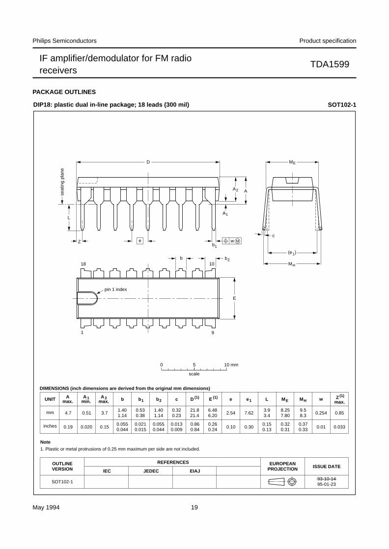
DIP18: plastic dual in-line package; 18 leads (300 mil) SOT102-1
May 1994 20
Philips Semiconductors Product specification
IF amplifier/demodulator for FM radioreceivers
TDA1599
UNITA
max. A1 A2 A3 bp c D (1) E (1) (1)e HE L Lp Q Zywv θ
REFERENCESOUTLINEVERSION
EUROPEANPROJECTION ISSUE DATE
IEC JEDEC EIAJ
mm
inches
2.65 0.300.10
2.452.25
0.490.36
0.320.23
13.012.6
7.67.4 1.27
10.6510.00
1.11.0
0.90.4 8
0
o
o
0.25 0.1
DIMENSIONS (inch dimensions are derived from the original mm dimensions)
Note
1. Plastic or metal protrusions of 0.15 mm maximum per side are not included.
1.10.4
SOT163-192-11-1795-01-24
10
20
w Mbp
detail X
Z
e
11
1
D
y
0.25
075E04 MS-013AC
pin 1 index
0.10 0.0120.004
0.0960.089
0.0190.014
0.0130.009
0.510.49
0.300.29 0.050
1.4
0.0550.420.39
0.0430.039
0.0350.0160.01
0.25
0.01 0.0040.0430.0160.01
0 5 10 mm
scale
X
θ
AA1
A2
HE
Lp
Q
E
c
L
v M A
(A )3
A
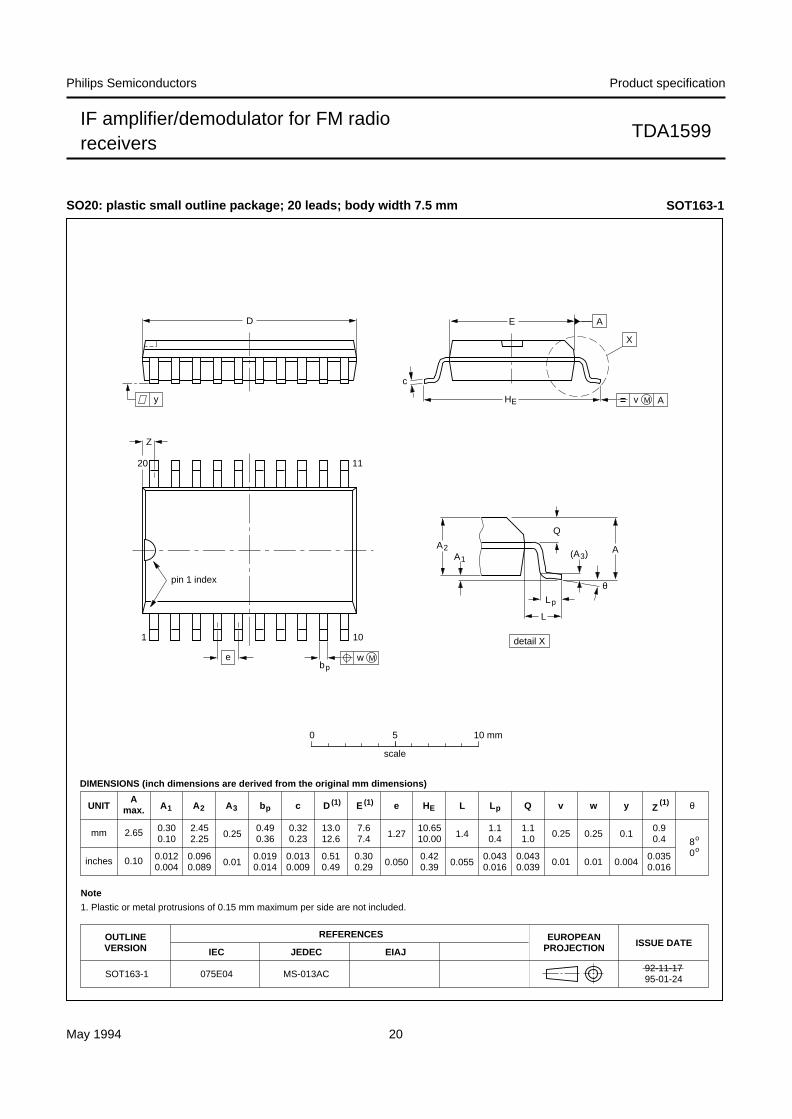
SO20: plastic small outline package; 20 leads; body width 7.5 mm SOT163-1
May 1994 21
Philips Semiconductors Product specification
IF amplifier/demodulator for FM radioreceivers
TDA1599
SOLDERING
Introduction
There is no soldering method that is ideal for all ICpackages. Wave soldering is often preferred whenthrough-hole and surface mounted components are mixedon one printed-circuit board. However, wave soldering isnot always suitable for surface mounted ICs, or forprinted-circuits with high population densities. In thesesituations reflow soldering is often used.
This text gives a very brief insight to a complex technology.A more in-depth account of soldering ICs can be found inour “IC Package Databook” (order code 9398 652 90011).
DIP
SOLDERING BY DIPPING OR BY WAVE
The maximum permissible temperature of the solder is260 °C; solder at this temperature must not be in contactwith the joint for more than 5 seconds. The total contacttime of successive solder waves must not exceed5 seconds.
The device may be mounted up to the seating plane, butthe temperature of the plastic body must not exceed thespecified maximum storage temperature (Tstg max). If theprinted-circuit board has been pre-heated, forced coolingmay be necessary immediately after soldering to keep thetemperature within the permissible limit.
REPAIRING SOLDERED JOINTS
Apply a low voltage soldering iron (less than 24 V) to thelead(s) of the package, below the seating plane or notmore than 2 mm above it. If the temperature of thesoldering iron bit is less than 300 °C it may remain incontact for up to 10 seconds. If the bit temperature isbetween 300 and 400 °C, contact may be up to 5 seconds.
SO
REFLOW SOLDERING
Reflow soldering techniques are suitable for all SOpackages.
Reflow soldering requires solder paste (a suspension offine solder particles, flux and binding agent) to be appliedto the printed-circuit board by screen printing, stencilling orpressure-syringe dispensing before package placement.
Several techniques exist for reflowing; for example,thermal conduction by heated belt. Dwell times varybetween 50 and 300 seconds depending on heatingmethod. Typical reflow temperatures range from215 to 250 °C.
Preheating is necessary to dry the paste and evaporatethe binding agent. Preheating duration: 45 minutes at45 °C.
WAVE SOLDERING
Wave soldering techniques can be used for all SOpackages if the following conditions are observed:
• A double-wave (a turbulent wave with high upwardpressure followed by a smooth laminar wave) solderingtechnique should be used.
• The longitudinal axis of the package footprint must beparallel to the solder flow.
• The package footprint must incorporate solder thieves atthe downstream end.
During placement and before soldering, the package mustbe fixed with a droplet of adhesive. The adhesive can beapplied by screen printing, pin transfer or syringedispensing. The package can be soldered after theadhesive is cured.
Maximum permissible solder temperature is 260 °C, andmaximum duration of package immersion in solder is10 seconds, if cooled to less than 150 °C within6 seconds. Typical dwell time is 4 seconds at 250 °C.
A mildly-activated flux will eliminate the need for removalof corrosive residues in most applications.
REPAIRING SOLDERED JOINTS
Fix the component by first soldering two diagonally-opposite end leads. Use only a low voltage soldering iron(less than 24 V) applied to the flat part of the lead. Contacttime must be limited to 10 seconds at up to 300 °C. Whenusing a dedicated tool, all other leads can be soldered inone operation within 2 to 5 seconds between270 and 320 °C.

May 1994 22
Philips Semiconductors Product specification
IF amplifier/demodulator for FM radioreceivers
TDA1599
DEFINITIONS
LIFE SUPPORT APPLICATIONS
These products are not designed for use in life support appliances, devices, or systems where malfunction of theseproducts can reasonably be expected to result in personal injury. Philips customers using or selling these products foruse in such applications do so at their own risk and agree to fully indemnify Philips for any damages resulting from suchimproper use or sale.
Data sheet status
Objective specification This data sheet contains target or goal specifications for product development.
Preliminary specification This data sheet contains preliminary data; supplementary data may be published later.
Product specification This data sheet contains final product specifications.
Limiting values
Limiting values given are in accordance with the Absolute Maximum Rating System (IEC 134). Stress above one ormore of the limiting values may cause permanent damage to the device. These are stress ratings only and operationof the device at these or at any other conditions above those given in the Characteristics sections of the specificationis not implied. Exposure to limiting values for extended periods may affect device reliability.
Application information
Where application information is given, it is advisory and does not form part of the specification.