1 CMOS R&D for STAR Wieman RNC LBNL Snowmass Review of current R&D and technologies session SG3-1...
28
1 CMOS R&D for STAR Wieman RNC LBNL Snowmass Review of current R&D and technologies session SG3-1 Fri 18 August 2005 1:30-5:00 Pyramid Room
-
Upload
helen-bradley -
Category
Documents
-
view
213 -
download
0
Transcript of 1 CMOS R&D for STAR Wieman RNC LBNL Snowmass Review of current R&D and technologies session SG3-1...
1
CMOS R&D for STAR
Wieman RNCLBNL
Snowmass Review of current R&D and technologiessession SG3-1Fri 18 August 2005 1:30-5:00Pyramid Room

2
Things to cover
Some work on a photo-gate, an attempted improvement on the CMOS pixels, understanding the problem
Forward bias diode, short decay time Avalanche effect in APS, why no gain? Projects in the pipe

3
Y. Chen, S. Kleinfelder, A. Koohi, S. Li University of California, Irvine, California
H. Huang, A. TaiUniversity of California, Los Angeles, California 90095
V. Kushpil, M. SumberaNuclear Physics Institute AS CR, 250 68 Rez/Prague, Czech Republic
C. Colledani, W. Dulinski, A. Himmi, C. Hu, A. Shabetai, M. Szelezniak, I. Valin, M. Winter
Institut de Recherches Subatomique, Strasbourg, FranceF. Bieser, R. Gareus, L. Greiner, H.S. Matis, M. Oldenburg, H.G.
Ritter, L. Pierpoint, F. Retiere, A. Rose, K. Schweda, E. Sichtermann, J.H. Thomas, H. Wieman, E. Yamamoto
Lawrence Berkeley National Laboratory, Berkeley, California 94720
STAR CMOS R&D Participants

4
With the standard CMOS pixel array off chip CDS is required to remove fixed pattern noise and KTC reset noise
In the standard CMOS pixel array the signal is spread over multiple diodes
Penalty in signal to noise Potential advantages of photo-
gate Use like CCD – read voltage,
transfer charge – read voltage again and take difference. Gives on chip CDS
Increase signal by reducing signal spreading to adjacent pixels. The photo gate permits large geometry without adding capacitance to the sense node.
Photo gate purpose – to address standard pixel limitations
P-
P
P+
Standard diode geometry

5
First silicon tests
Photo-gate directly to sense node drain
DC bias:V photo-gate 0.6 VV drain 2.4 V
Accumulated histogram of output signal for Fe55 X-ray test after CDS correction
Signal spreading Reduced gain
Issues:

6
Photo-gate LED test
Used a single pixel in sector 5 (simple structure with photo-gate and small drain on the edge) Photo-gate voltage 1 volt Drain voltage set by full reset
voltage Test sequence
Reset all pixels Clock row and column shift
registers to select a single pixel
Inject 2 red LED pulses Observe output voltage with
oscilloscope throughout sequence
Also did same test with sector 1 ( the standard diode) for comparison
Sector 5
Photo-gate
drain
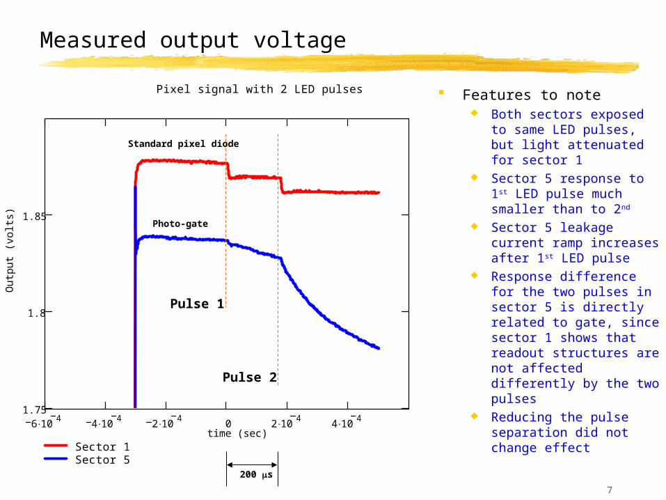
7
Measured output voltage
Pixel signal with 2 LED pulses
6 104
4 104
2 104
0 2 104
4 104
1.75
1.8
1.85
Sector 1Sector 5
time (sec)
Out
put (
volts
)
Pulse 1
Pulse 2
Features to note Both sectors exposed to
same LED pulses, but light attenuated for sector 1
Sector 5 response to 1st LED pulse much smaller than to 2nd
Sector 5 leakage current ramp increases after 1st LED pulse
Response difference for the two pulses in sector 5 is directly related to gate, since sector 1 shows that readout structures are not affected differently by the two pulses
Reducing the pulse separation did not change effect
Standard pixel diode
Photo-gate
200 s

8
Photo-gate time response to two pulses the same, only amplitude difference
Pixel signal with 2 LED pulses
6 104
4 104
2 104
0 2 104
4 104
1.75
1.8
1.85
Sector 1Sector 5
time (sec)
Out
put (
volts
)
Pulse 1
Pulse 2
Adjust amplitude and overlay
Signal fits:
t
exp1
+ plus leakage slope
204 s

9
Photo-gate
Test chip Measured charge transfer (200 s) Shows saturation effects
Has been suggested that surface states at the oxide silicon are the cause
Quantitative check of Transfer delay Saturation Leakage current (large, another feature of the gate)

10
Conditions under the gate in the p epi layer
p- epi p- epi with n type drain
In thermal equilibrium p silicon inverted with accumulation of electrons under the gate
Addition of drain removes electrons leaving depleted region
Depleted space charge region
Field free region, saturated with mobile holes

11
First step of electron collection
Diffusing electrons caught in the vertical space charge field under the gate
GateDrain
Electrons distribute along the surface

12
Check of time constants for different processes tells if surface traps are a reasonable explanation for slow transfer
GateDrain
Idirect
Direct drain current
Itrapped
Trapping current
Idelayed
Detrapping drain current
Surface states
dTime constant for direct diffusion to the drain
Time constant for capture by the traps
Time constant for release from the trapsr
c
If d > c will be trapped
If r is large transfer is delayed

13
Simple diffusion transfer of electrons from gate to drain
tnd
dD n 2
xnd
d
2
n electron density
Dnelectron diffusion constant in silicon
Diffusion equation in 1D
Solve with COSMOS FEA (~3D) – thermal transient solution, analogous diffusion equation
Result:
d = 120 ns
Start with uniform temperature and a heat
sink at the drain
Convert to electron diffusion
photo-gate
drain
drain total electrons under gateN t( ) N 0 expt
d

14
Energy window for contributing traps – how many traps
Less than 100 s decay time
Sze
Traps already filled
Decay time constant back to the conduction band, Zhang Li paper
E trap energy separation from the conduction band
vththermal electron velocity
ncross section
NcEffective density of conduction band states
Nst 2.6 109
1
cm2
Nst Ag 1 104 Number of
contributing traps
More than 15 ms decay time
r1
v th n N c expE
k b T

15
Time constants show delay
d = 120 ns
c = 75 ns
r = 100 s
Capture time easy to calculate, depends on surface trap density, the vertical density profile of the electrons. Surface trap density from literature, determined from capacitance measured as a function of frequency
Trap release time depends on trap energy relative to conduction band. Only counted traps with decay times > 100 s
Capture time for 100 s traps is less than the direct diffusion time to the drain, so trap delay is expected.
Diffusion time constant

16
Number of empty traps is consistent with measured effects
10000 - The number of empty traps from the published densities which are empty and have a lifetime of more than 100 s A trapping time ( 75 ns ), less than diffusion time A consistent with saturation by the estimated 4000 photo
generated electrons. Another reason why photo gate won’t work for us, our signals are too small to saturate the traps.

17
Surface traps also explain large leakage current
Calculated surface generated current using Reed Schockley Hall
32 fA
Based on literature values of surface trap density and the width of the mid gap energy window contributing to thermally generated current
Measured leakage 17 fA
This large leakage current is another feature of the photo gate making it unsuitable for our application. Since, it appears that the surface traps are the problem, the only obvious solution for this approach is buried channels
Close enough
18
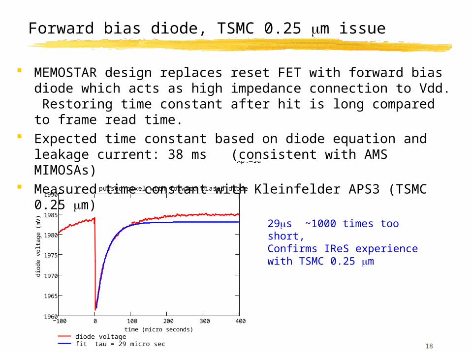
Forward bias diode, TSMC 0.25 m issue
MEMOSTAR design replaces reset FET with forward bias diode which acts as high impedance connection to Vdd. Restoring time constant after hit is long compared to frame read time.
Expected time constant based on diode equation and leakage current: 38 ms (consistent with AMS MIMOSAs)
Measured time constant with Kleinfelder APS3 (TSMC 0.25 m)Xp submatrix M1 115 last M1 0 0 1 0
100 0 100 200 300 4001960
1965
1970
1975
1980
1985
1990
diode voltagefit tau = 29 micro sec
pulsed pixel with forward biased diode
time (micro seconds)
diod
e vo
ltage
(m
V)
29s ~1000 times too short, Confirms IReS experience with TSMC 0.25 m

19
Avalanche gain, why not?
Output voltage of pixel diode. Droop is due to impact ionization in the source follower FET, S. Maestre et al.
Injected signal from 3 equal amplitude LED flashes
Microscopic view shows identical step size. Why no gain on the third pulse?
Kleinfelder APS-3 sector 1
20
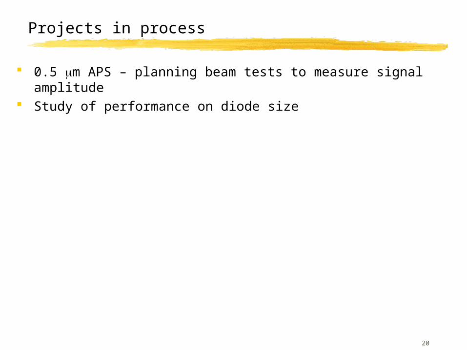
Projects in process
0.5 m APS – planning beam tests to measure signal amplitude Study of performance on diode size

21
Photo gate summary
Some questions remain, but surface traps could explain photo-gate behavior They provide delay on right order They seem to have right number to see saturation effects They are consistent with observed leakage current
Note, both Turchetta and Janesick tell me they have tried and failed to make a working photo-gate in standard CMOS. Janesick saw the same type of delayed signal
Janesick has made photo-gates work using a special process from Jazz Semiconductor with buried channel -- big bucks
Will there eventually be a photo process that available to us with buried channel?

22
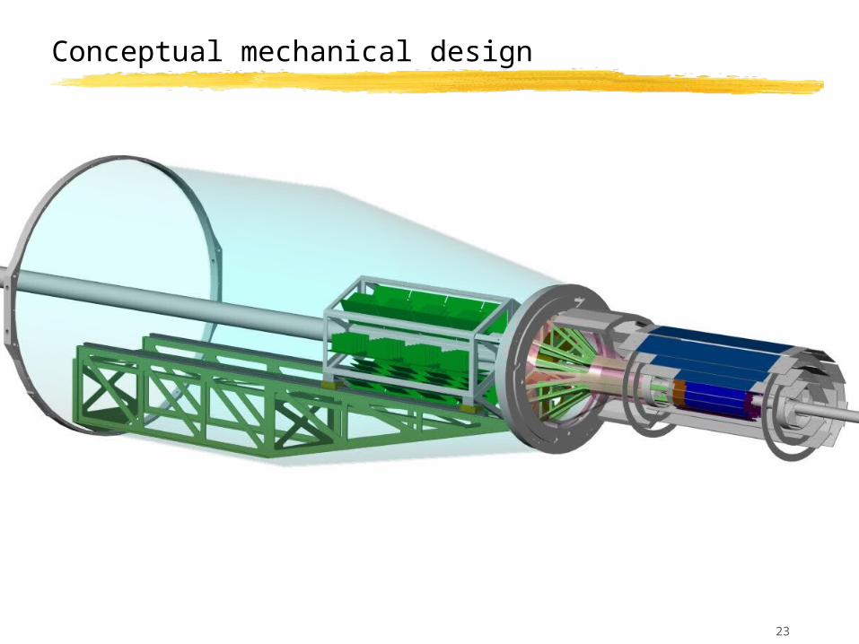
STAR Micro Vertex Detector
Two layers 1.5 cm radius 4.5 cm radius
24 ladders 2 cm X 20 cm each < 0.3% X0
~ 100 Mega Pixels
Purpose:Greatly improve D meson capability in STAR
23
Conceptual mechanical design

24

25
Drain current after light injection
Nano amp drain current
Rapid electron transfer - complete in 60 ns
photo gate
transfer gate drain
Light injection
60 nsSimulation using SILVACO ATLAS running on laptop. Service through eecad, only a few 10s of dollars to run. About to change to per day cost of ~$170
Relied on Zhang Li and Wei Chen to get started
26
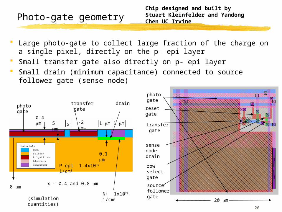
photo gate
source follower gate
reset gate
transfer gate
row select gate
sense node drain
Large photo-gate to collect large fraction of the charge on a single pixel, directly on the p- epi layer
Small transfer gate also directly on p- epi layer Small drain (minimum capacitance) connected to source follower gate
(sense node)
Photo-gate geometry
20 m
x -2 m- 1 m 1 m5 nm
8 m
0.1 m
0.4 m
P epi 1.4x10¹⁵ 1/cm3
N+ 1x10²⁰ 1/cm3
photo gate transfer gate
drain
x = 0.4 and 0.8 m
(simulation quantities)
Chip designed and built by Stuart Kleinfelder and Yandong Chen UC Irvine

27
Density of electrons at the surface left by LED
transient layer of 4000 electrons left by LED signal under 20 m 20 m gate
electron density distribution under the gate
The static electron density n(y) set by condition that diffusion and drift cancel
Dn ynd
d E y( ) n n 0
use Einstein relation Dn
kb T
qe
n
Debye length LD
kb T s
NA qe2
= 110 nm
depletion depth d2 vs s
NA qe = 960 nm
d
y
LED
n y( ) ns expd y
LD2
solution
nsd Ntotal
LD2
Ag ns 8 10
141
cm3
Integrate over volume under gate to get ns
1/e distance = 12 nm

28
tNe
d
dvth n Nst Ag ns rate of loss of electrons into surface states, see Zhang Li and H.
Kramer
vthelectron thermal velocity
nsurface state capture cross section
Nstsurface state density, from Sze
Agarea of the capture surface
nselectron density at the surface (from last page)
Rate of capture into surface states
Capture to surface states faster than direct diffusion to drain therefore surface states will affect transfer rate
st = 75 ns < n = 120 ns
capture direct diffusion
Measured by C vs freq, see Sze
Use number of empty traps
tNe
d
d
Ne
st
st
LD2
d vth n Nst 75ns time constant for capture