
1 Bipolar Junction Transistors (BJTs). Copyright 2004 by Oxford University Press, Inc....
198
1 Bipolar Junction Transistors (BJTs)
-
date post
20-Dec-2015 -
Category
Documents
-
view
248 -
download
8
Transcript of 1 Bipolar Junction Transistors (BJTs). Copyright 2004 by Oxford University Press, Inc....

1
Bipolar JunctionTransistors (BJTs)
Microelectronic Circuits - Fifth Edition Sedra/Smith 2Copyright 2004 by Oxford University Press, Inc.
• Bipolar Junction Transistors, BJT, a three terminal, non-linear electronic device.
• BJT’s are used as amplifiers in analog electronics.
• BJTs are used as switches in digital electronics.
• Invented in 1948 by Bardeen, Brattain, and Shockley at Bell Telephone Labs.
• Popular for three decades before being overtaken by Field Effect Transistors, FETs.
Microelectronic Circuits - Fifth Edition Sedra/Smith 3Copyright 2004 by Oxford University Press, Inc.
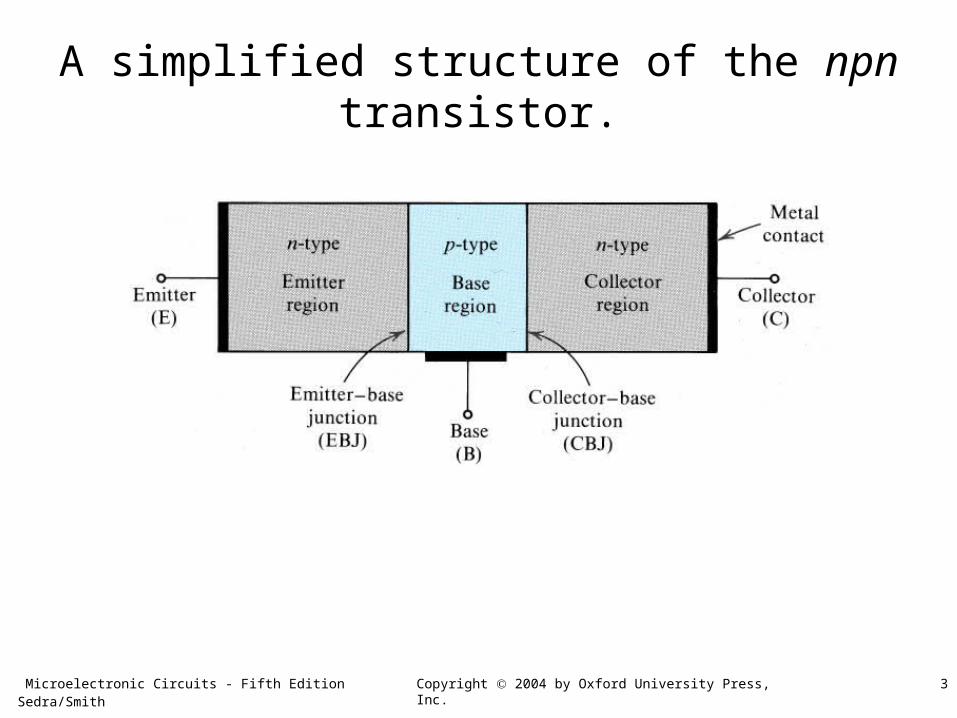
A simplified structure of the npn transistor.
Microelectronic Circuits - Fifth Edition Sedra/Smith 4Copyright 2004 by Oxford University Press, Inc.
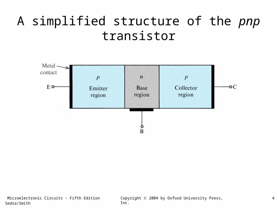
A simplified structure of the pnp transistor
Microelectronic Circuits - Fifth Edition Sedra/Smith 5Copyright 2004 by Oxford University Press, Inc.
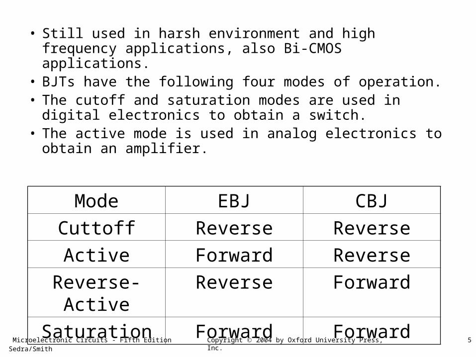
• Still used in harsh environment and high frequency applications, also Bi-CMOS applications.
• BJTs have the following four modes of operation.• The cutoff and saturation modes are used in digital
electronics to obtain a switch.• The active mode is used in analog electronics to obtain
an amplifier.
Mode EBJ CBJ
Cuttoff Reverse Reverse
Active Forward Reverse
Reverse-Active Reverse Forward
Saturation Forward Forward
Microelectronic Circuits - Fifth Edition Sedra/Smith 6Copyright 2004 by Oxford University Press, Inc.
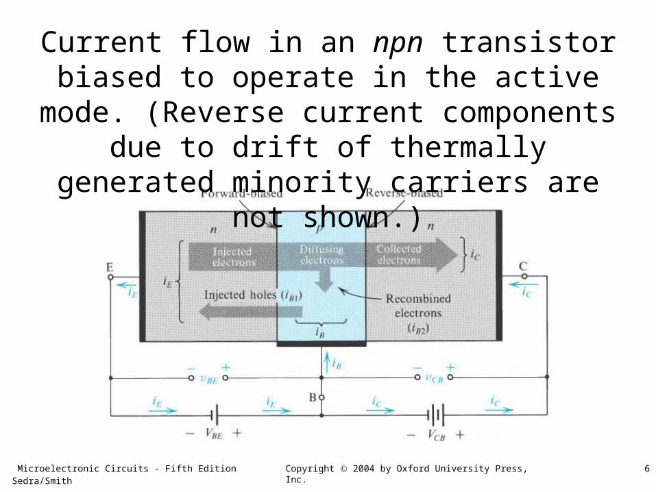
Current flow in an npn transistor biased to operate in the active mode. (Reverse current
components due to drift of thermally generated minority carriers are not shown.)

Microelectronic Circuits - Fifth Edition Sedra/Smith 7Copyright 2004 by Oxford University Press, Inc.
• Ignore the very small drift currents.
• The EBJ is a forward biased pn junction.
• Holes are injected from the base to the emitter and electrons injected from the emitter to the base.
• These two components combine to form the emitter current, iE.
• A highly doped emitter and a lightly doped base keep the hole component of iE small.
Microelectronic Circuits - Fifth Edition Sedra/Smith 8Copyright 2004 by Oxford University Press, Inc.
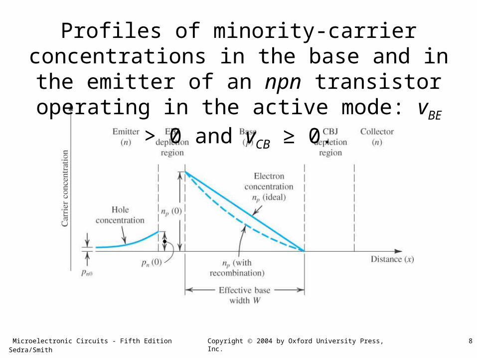
Profiles of minority-carrier concentrations in the base and in the emitter of an npn transistor
operating in the active mode: vBE > 0 and vCB ≥ 0.
Microelectronic Circuits - Fifth Edition Sedra/Smith 9Copyright 2004 by Oxford University Press, Inc.
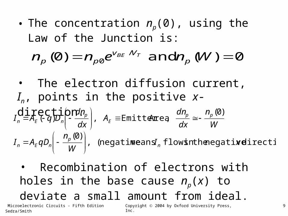
• The concentration np(0), using the Law of the Junction is:
0)(and)0( /0 Wnenn p
Vvpp
TBE
• The electron diffusion current, In, points in the positive x-direction.
direction)negativetheinflowsmeansnegative(,)0(
)0(,AreaEmitter,)(
xIW
nqDAI
W
n
dx
dnA
dx
dnDqAI
np
nEn
ppE
pnEn
• Recombination of electrons with holes in the base cause np(x) to deviate a small amount from ideal.

Microelectronic Circuits - Fifth Edition Sedra/Smith 10Copyright 2004 by Oxford University Press, Inc.
• The collector current, ic, points in the negative x-direction and is equal in magnitude to In.
WN
nqDAIwhereeIi
N
nne
W
nqDAi
ennW
nqDAi
Ii
A
inEs
VvsC
A
ip
VvpnEC
Vvpp
pnEC
nC
TBE
TBE
TBE
2/
2
0/0
/0
,
,
)0(,)0(
• The collector current is directly proportional to the emitter area, AE, and inversely proportional to the effective width of the base, W.
Microelectronic Circuits - Fifth Edition Sedra/Smith 11Copyright 2004 by Oxford University Press, Inc.
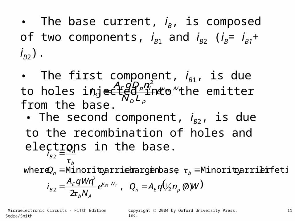
• The base current, iB, is composed of two components, iB1 and iB2 (iB= iB1+ iB2).
• The first component, iB1, is due to holes injected into the emitter from the base.
TBE Vv
pD
ipEB e
LN
nqDAi /
2
1
• The second component, iB2, is due to the recombination of holes and electrons in the base.
WnqAQeN
qWnAi
Q
Qi
pEnVv
Ab
iEB
bn
b
nB
TBE )0(,2
lifetimecarrierMinority,baseinchargecarrierMinoritywhere
21/
2
2
2
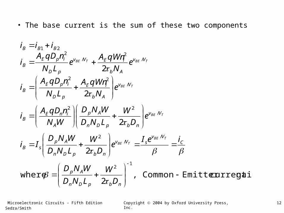
Microelectronic Circuits - Fifth Edition Sedra/Smith 12Copyright 2004 by Oxford University Press, Inc.
• The base current is the sum of these two components
gaincurrentEmitterCommon,2
where
2
2
2
2
12
//
2
/22
/22
/2
/2
21
nbpDn
Ap
CVv
sVv
nbpDn
ApsB
Vv
nbpDn
Ap
A
inEB
Vv
Ab
iE
pD
ipEB
Vv
Ab
iEVv
pD
ipEB
BBB
D
W
LND
WND
ieIe
D
W
LND
WNDIi
eD
W
LND
WND
WN
nqDAi
eN
qWnA
LN
nqDAi
eN
qWnAe
LN
nqDAi
iii
TBE
TBE
TBE
TBE
TBETBE

Microelectronic Circuits - Fifth Edition Sedra/Smith 13Copyright 2004 by Oxford University Press, Inc.
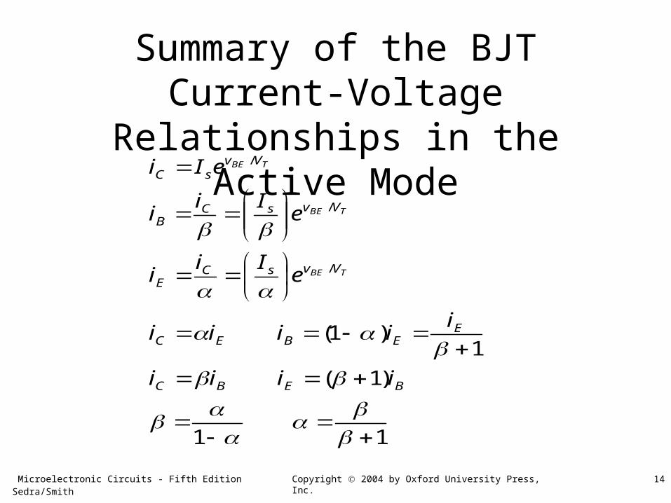
• The emitter current, iE, (using KCL) is equal to the base current plus the collector current.
gaincurrentBaseCommon,1
,
1
1
/
/
CVvsE
VvsE
CC
CE
BCE
ie
Ii
eIi
ii
ii
iii
TBE
TBE
• α = αF, β = βF forward active mode, αR and βR for the reverse active mode.
Microelectronic Circuits - Fifth Edition Sedra/Smith 14Copyright 2004 by Oxford University Press, Inc.
Summary of the BJT Current-Voltage Relationships in the Active Mode
11
)1(
1)1(
/
/
/
BEBC
EEBEC
VvsCE
VvsCB
VvsC
iiii
iiiii
eIi
i
eIi
i
eIi
TBE
TBE
TBE

Microelectronic Circuits - Fifth Edition Sedra/Smith 15Copyright 2004 by Oxford University Press, Inc.
Large-signal equivalent-circuit models of the npn BJT operating in the forward active mode.
Microelectronic Circuits - Fifth Edition Sedra/Smith 16Copyright 2004 by Oxford University Press, Inc.
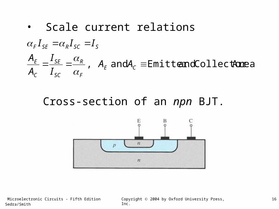
• Scale current relations
AreasCollectorandEmitterand,
CEF
R
SC
SE
C
E
SSCRSEF
AAI
I
A
A
III
Cross-section of an npn BJT.

Microelectronic Circuits - Fifth Edition Sedra/Smith 17Copyright 2004 by Oxford University Press, Inc.
Model for the npn transistor when operated in the reverse active mode (i.e., with the CBJ
forward biased and the EBJ reverse biased).

Microelectronic Circuits - Fifth Edition Sedra/Smith 18Copyright 2004 by Oxford University Press, Inc.
The Ebers-Moll (EM) model of the npn transistor.
Microelectronic Circuits - Fifth Edition Sedra/Smith 19Copyright 2004 by Oxford University Press, Inc.
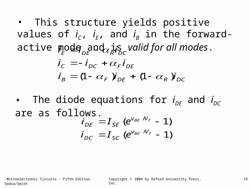
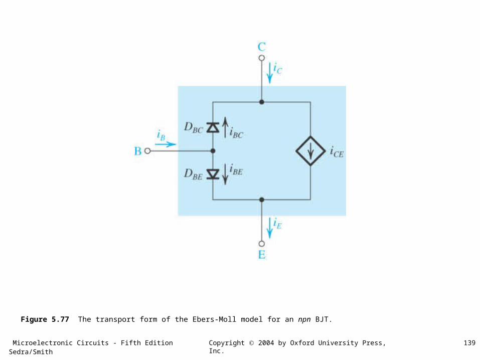
• This structure yields positive values of iC, iE, and iB in the forward-active mode and is valid for all modes.
DCRDEFB
DEFDCC
DCRDEE
iii
iii
iii
)1()1(
• The diode equations for iDE and iDC are as follows.
)1(
)1(/
/
TBC
TBE
VvSCDC
VvSEDE
eIi
eIi

Microelectronic Circuits - Fifth Edition Sedra/Smith 20Copyright 2004 by Oxford University Press, Inc.
• Substituting the diode equations into the expressions for iC, iE, and iB and using the scale current relations we obtain the following equations.
)1()1(
)1()1(
)1()1(
//
//
//
TBCTBE
TBCTBE
TBCTBE
Vv
R
SVv
F
SB
Vv
R
SVvSC
VvS
Vv
F
SE
eI
eI
i
eI
eIi
eIeI
i
Microelectronic Circuits - Fifth Edition Sedra/Smith 21Copyright 2004 by Oxford University Press, Inc.
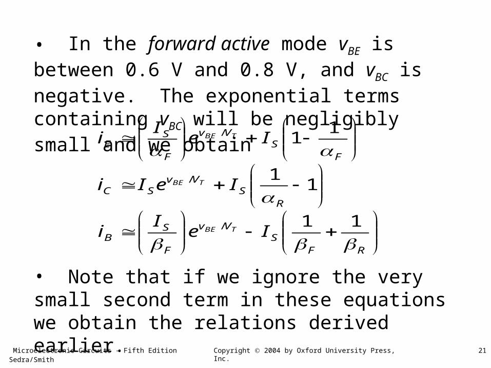
• In the forward active mode vBE is between 0.6 V and 0.8 V, and vBC is negative. The exponential terms containing vBC will be negligibly small and we obtain
RFS
Vv
F
SB
RS
VvSC
FS
Vv
F
SE
IeI
i
IeIi
IeI
i
TBE
TBE
TBE
11
11
11
/
/
/
• Note that if we ignore the very small second term in these equations we obtain the relations derived earlier.

Microelectronic Circuits - Fifth Edition Sedra/Smith 22Copyright 2004 by Oxford University Press, Inc.
The iC –vCB characteristic of an npn transistor fed with a constant emitter current IE. The transistor enters the saturation mode of
operation for vCB < –0.4 V, and the collector current diminishes.

Microelectronic Circuits - Fifth Edition Sedra/Smith 23Copyright 2004 by Oxford University Press, Inc.
Concentration profile of the minority carriers (electrons) in the base of an npn transistor operating in
the saturation mode.
TBCTBE Vv
R
SVvSC e
IeIi //
Ignoring small terms:
0)( /0 TBC Vv
pp enWn
Law of the Junction:
Microelectronic Circuits - Fifth Edition Sedra/Smith 24Copyright 2004 by Oxford University Press, Inc.
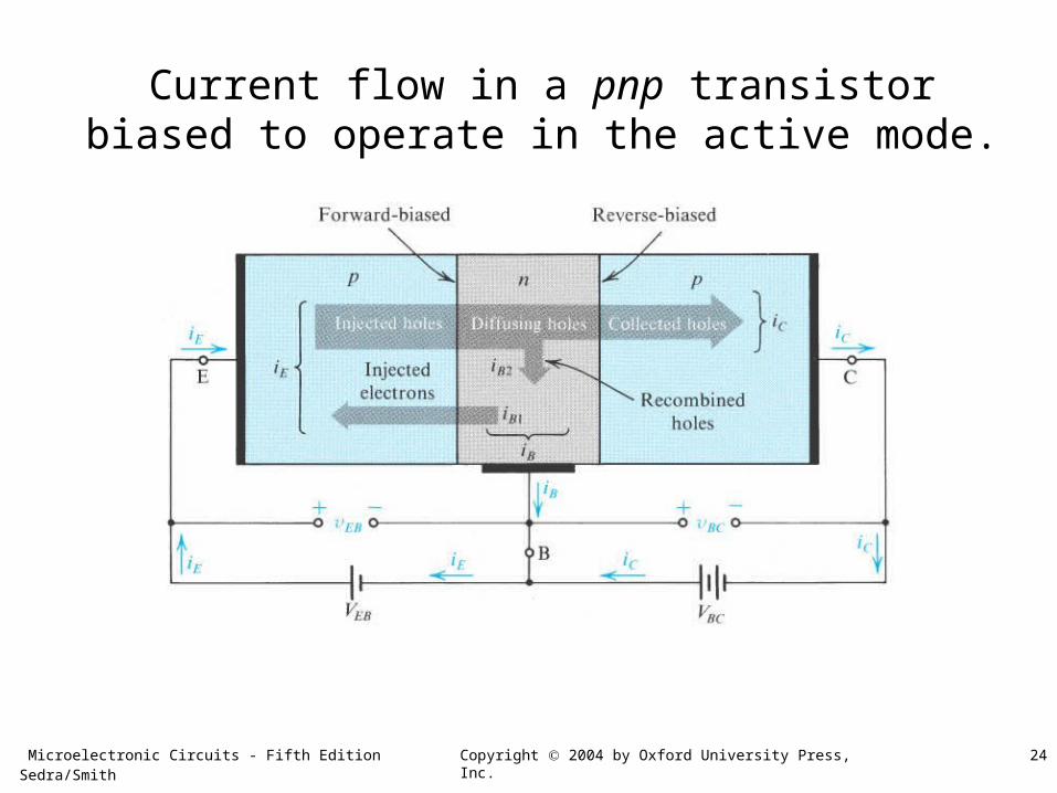
Current flow in a pnp transistor biased to operate in the active mode.

Microelectronic Circuits - Fifth Edition Sedra/Smith 25Copyright 2004 by Oxford University Press, Inc.
Large-signal model for the pnp transistor operating in the active mode.

Microelectronic Circuits - Fifth Edition Sedra/Smith 26Copyright 2004 by Oxford University Press, Inc.
Circuit symbols for BJTs.
Microelectronic Circuits - Fifth Edition Sedra/Smith 27Copyright 2004 by Oxford University Press, Inc.
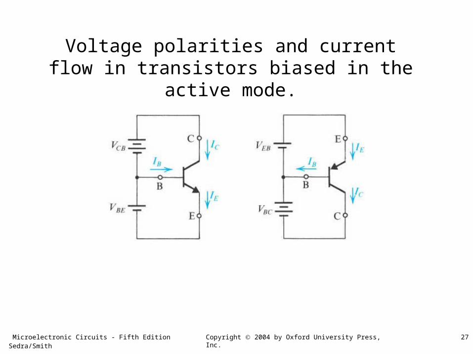
Voltage polarities and current flow in transistors biased in the active mode.
Microelectronic Circuits - Fifth Edition Sedra/Smith 28Copyright 2004 by Oxford University Press, Inc.
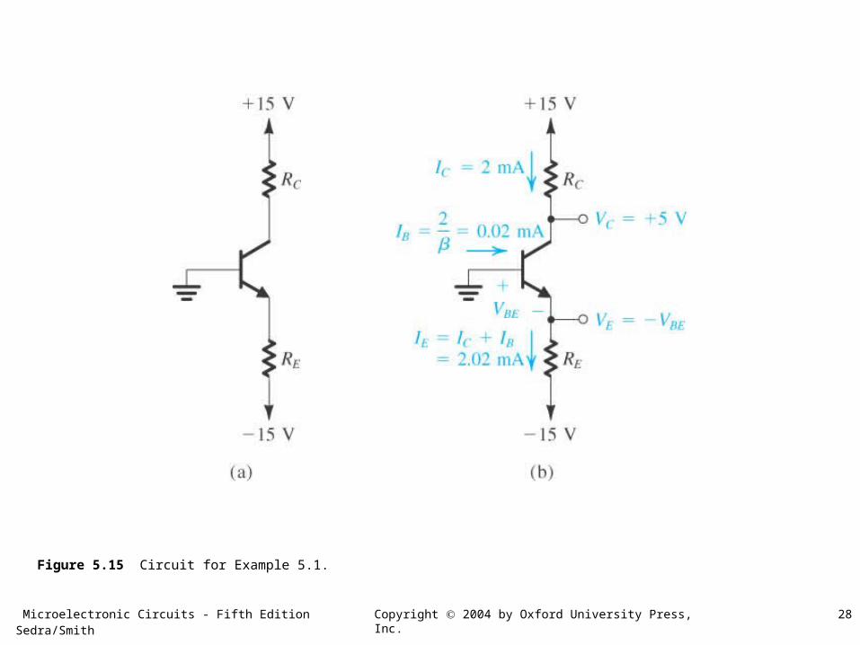
Figure 5.15 Circuit for Example 5.1.
Microelectronic Circuits - Fifth Edition Sedra/Smith 29Copyright 2004 by Oxford University Press, Inc.
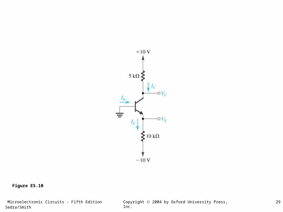
Figure E5.10

Microelectronic Circuits - Fifth Edition Sedra/Smith 30Copyright 2004 by Oxford University Press, Inc.
Figure E5.11
Microelectronic Circuits - Fifth Edition Sedra/Smith 31Copyright 2004 by Oxford University Press, Inc.
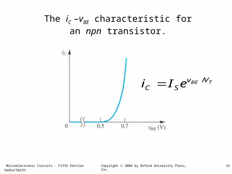
The iC –vBE characteristic for an npn transistor.
TBE VvSC eIi /
Microelectronic Circuits - Fifth Edition Sedra/Smith 32Copyright 2004 by Oxford University Press, Inc.
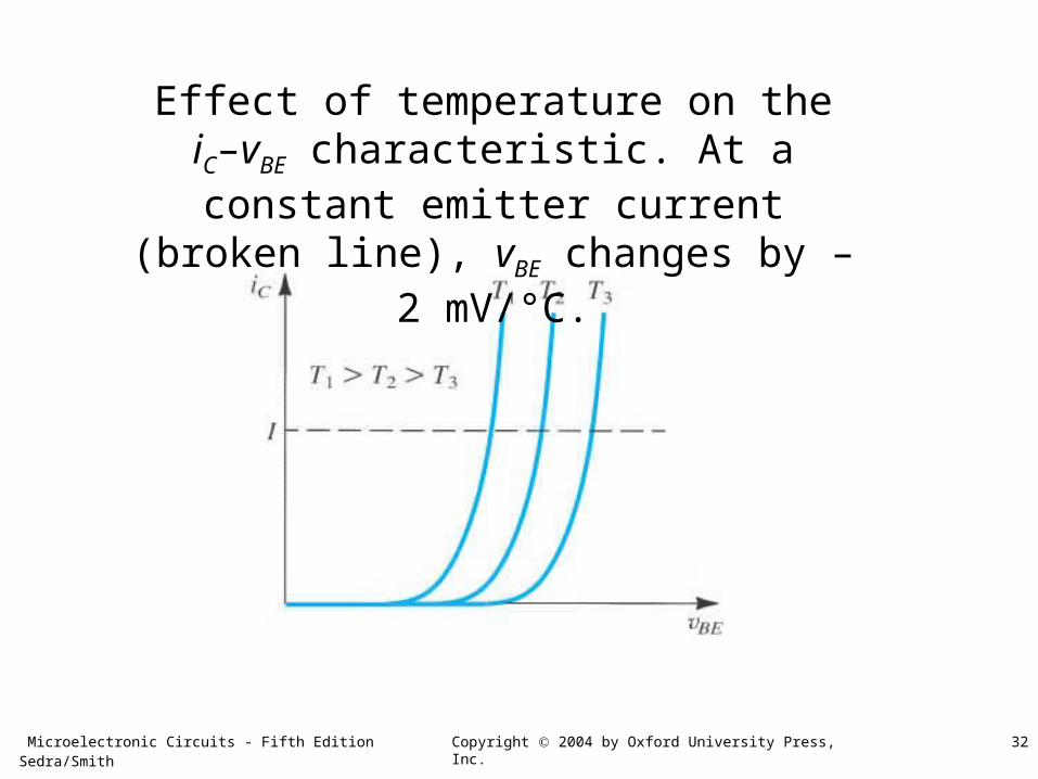
Effect of temperature on the iC–vBE characteristic. At a constant emitter current
(broken line), vBE changes by –2 mV/°C.
Microelectronic Circuits - Fifth Edition Sedra/Smith 33Copyright 2004 by Oxford University Press, Inc.
• Under normal forward-active and saturation modes vBE is between 0.6 V and 0.8 V.
• Use vBE ≈ 0.7 V for rapid calculation.

Microelectronic Circuits - Fifth Edition Sedra/Smith 34Copyright 2004 by Oxford University Press, Inc.
The iC–vCB characteristics of an npn transistor, common-base characteristic.
Microelectronic Circuits - Fifth Edition Sedra/Smith 35Copyright 2004 by Oxford University Press, Inc.
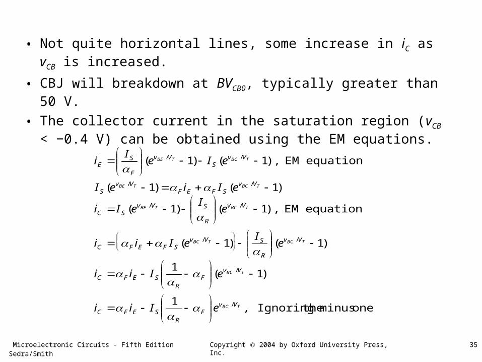
• Not quite horizontal lines, some increase in iC as vCB is increased.
• CBJ will breakdown at BVCB0, typically greater than 50 V.
• The collector current in the saturation region (vCB < −0.4 V) can be obtained using the EM equations.
one.minustheIgnoring,1
)1(1
)1()1(
equationEM),1()1(
)1()1(
equationEM),1()1(
/
/
//
//
//
//
TBC
TBC
TBCTBC
TBCTBE
TBCTBE
TBCTBE
VvF
RSEFC
VvF
RSEFC
Vv
R
SVvSFEFC
Vv
R
SVvSC
VvSFEF
VvS
VvS
Vv
F
SE
eIii
eIii
eI
eIii
eI
eIi
eIieI
eIeI
i
Microelectronic Circuits - Fifth Edition Sedra/Smith 36Copyright 2004 by Oxford University Press, Inc.
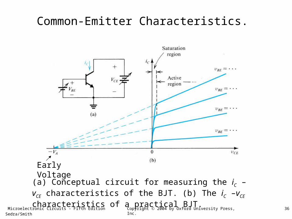
Common-Emitter Characteristics.
(a) Conceptual circuit for measuring the iC –vCE characteristics of the BJT. (b) The iC –vCE characteristics of a practical BJT.
Early Voltage

Microelectronic Circuits - Fifth Edition Sedra/Smith 37Copyright 2004 by Oxford University Press, Inc.
• The linear dependence of the collector current, iC, on the collector-emitter voltage, vCE, is called “The Early Effect”.
A
CEVvSC V
veIi TBE 1/
• The output resistance, ro
TBE
BE
VVS
Ao
vCE
Co
eI
Vr
v
ir
/
1
constant
Microelectronic Circuits - Fifth Edition Sedra/Smith 38Copyright 2004 by Oxford University Press, Inc.
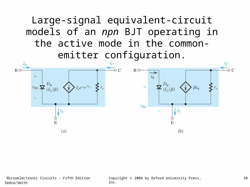
Large-signal equivalent-circuit models of an npn BJT operating in the active mode in the common-emitter
configuration.
Microelectronic Circuits - Fifth Edition Sedra/Smith 39Copyright 2004 by Oxford University Press, Inc.
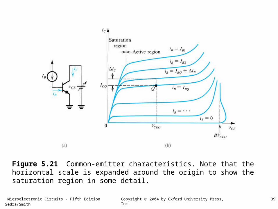
Figure 5.21 Common-emitter characteristics. Note that the horizontal scale is expanded around the origin to show the saturation region in some detail.

Microelectronic Circuits - Fifth Edition Sedra/Smith 40Copyright 2004 by Oxford University Press, Inc.
• Large-signal or dc CE current gain, βdc, (hFE in data books)
BQ
CQdc I
I
• Incremental or ac CE current gain, βac, (hfe in data books)
constant
CEvB
Cac i
i
• βdc and βac differ by 10% to 20%

Microelectronic Circuits - Fifth Edition Sedra/Smith 41Copyright 2004 by Oxford University Press, Inc.
• Typical dependence of β on IC and on temperature in a modern integrated-circuit npn silicon transistor intended for operation around 1 mA.

Microelectronic Circuits - Fifth Edition Sedra/Smith 42Copyright 2004 by Oxford University Press, Inc.
• An expanded view of the common-emitter characteristics in the saturation region.

Microelectronic Circuits - Fifth Edition Sedra/Smith 43Copyright 2004 by Oxford University Press, Inc.
• βac is high in the active region and low in the saturation region.
• IC,sat < βFIB
• βForced = IC,sat /IB < βF
• Overdrive factor: βF / βForced
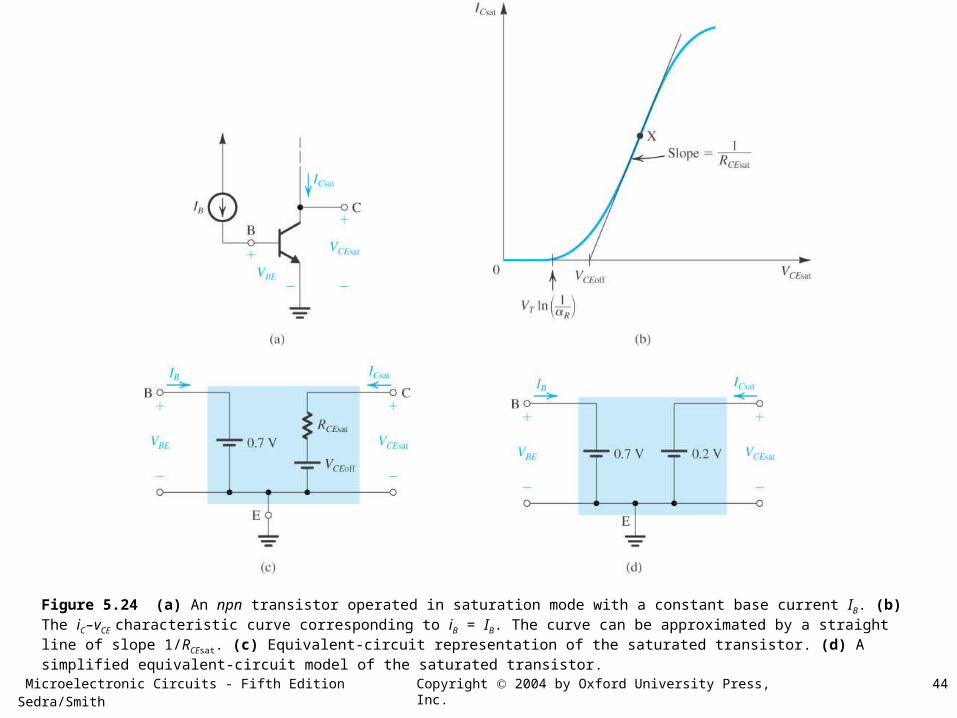
Microelectronic Circuits - Fifth Edition Sedra/Smith 44Copyright 2004 by Oxford University Press, Inc.
Figure 5.24 (a) An npn transistor operated in saturation mode with a constant base current IB. (b) The iC–vCE characteristic curve corresponding to iB = IB. The curve can be approximated by a straight line of slope 1/RCEsat. (c) Equivalent-circuit representation of the saturated transistor. (d) A simplified equivalent-circuit model of the saturated transistor.
Microelectronic Circuits - Fifth Edition Sedra/Smith 45Copyright 2004 by Oxford University Press, Inc.
• Saturation Resistance, RCEsat (~ 3 to 30 ohms)
CsatC
BBIiIiC
CECEsat i
vR
• Model of the saturated transistor
V2.0satsatoffsat CECCECE RIVV
• Using the EM equations for the saturated BJT one obtains the following expression for RCEsat.
)10/(1 BFCEsat IR
Microelectronic Circuits - Fifth Edition Sedra/Smith 46Copyright 2004 by Oxford University Press, Inc.
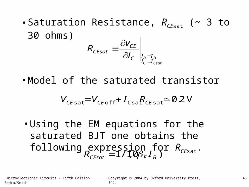
Figure 5.25 Plot of the normalized iC versus vCE for an npn transistor with F = 100 and R = 0.1. This is a plot of Eq. (5.47), which is derived using the Ebers-Moll model.

Microelectronic Circuits - Fifth Edition Sedra/Smith 47Copyright 2004 by Oxford University Press, Inc.
Figure E5.18
Microelectronic Circuits - Fifth Edition Sedra/Smith 48Copyright 2004 by Oxford University Press, Inc.
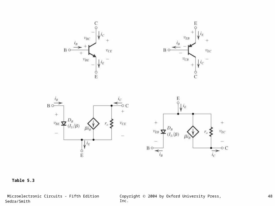
Table 5.3

Microelectronic Circuits - Fifth Edition Sedra/Smith 49Copyright 2004 by Oxford University Press, Inc.
Table 5.3 (Continued)
Microelectronic Circuits - Fifth Edition Sedra/Smith 50Copyright 2004 by Oxford University Press, Inc.
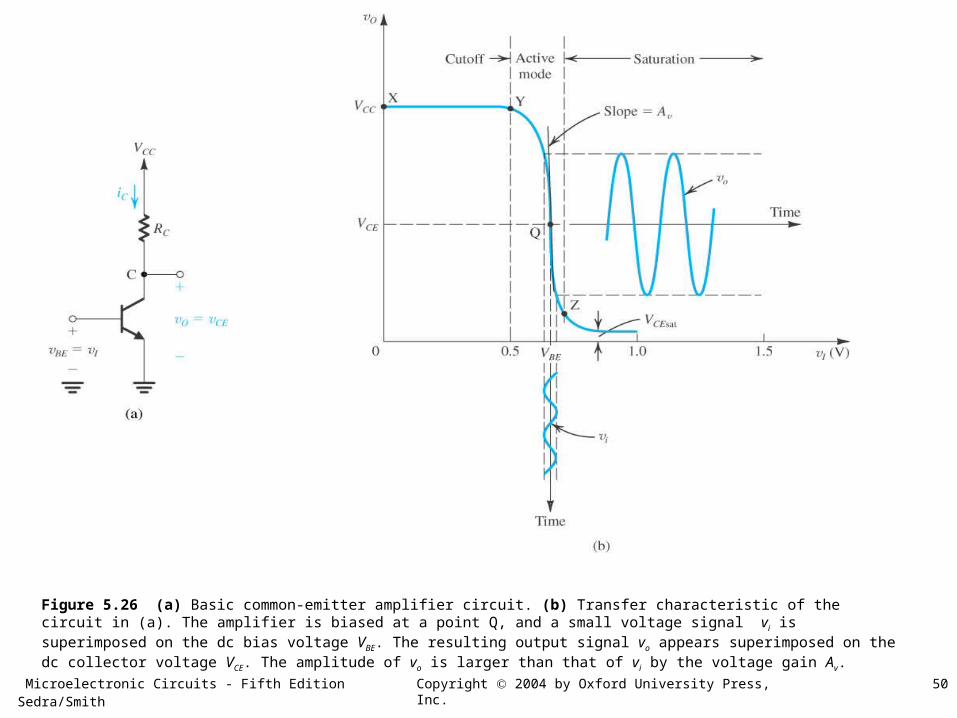
Figure 5.26 (a) Basic common-emitter amplifier circuit. (b) Transfer characteristic of the circuit in (a). The amplifier is biased at a point Q, and a small voltage signal vi is superimposed on the dc bias voltage VBE. The resulting output signal vo appears superimposed on the dc collector voltage VCE. The amplitude of vo is larger than that of vi by the voltage gain Av.
Microelectronic Circuits - Fifth Edition Sedra/Smith 51Copyright 2004 by Oxford University Press, Inc.
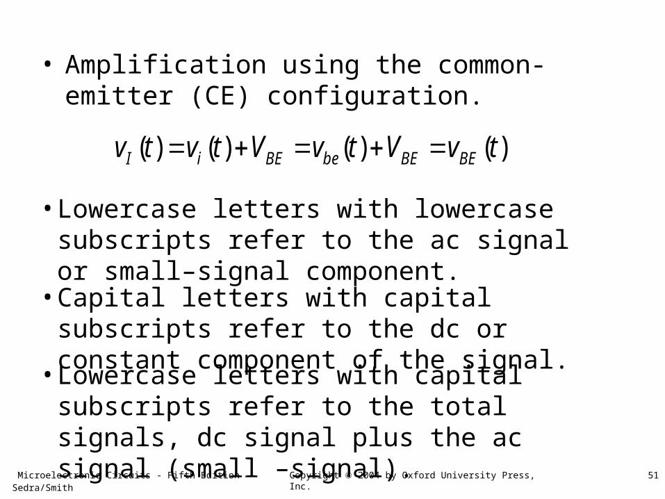
• Amplification using the common-emitter (CE) configuration.
)()()()( tvVtvVtvtv BEBEbeBEiI
• Lowercase letters with capital subscripts refer to the total signals, dc signal plus the ac signal (small –signal).
• Capital letters with capital subscripts refer to the dc or constant component of the signal.
• Lowercase letters with lowercase subscripts refer to the ac signal or small–signal component.
Microelectronic Circuits - Fifth Edition Sedra/Smith 52Copyright 2004 by Oxford University Press, Inc.
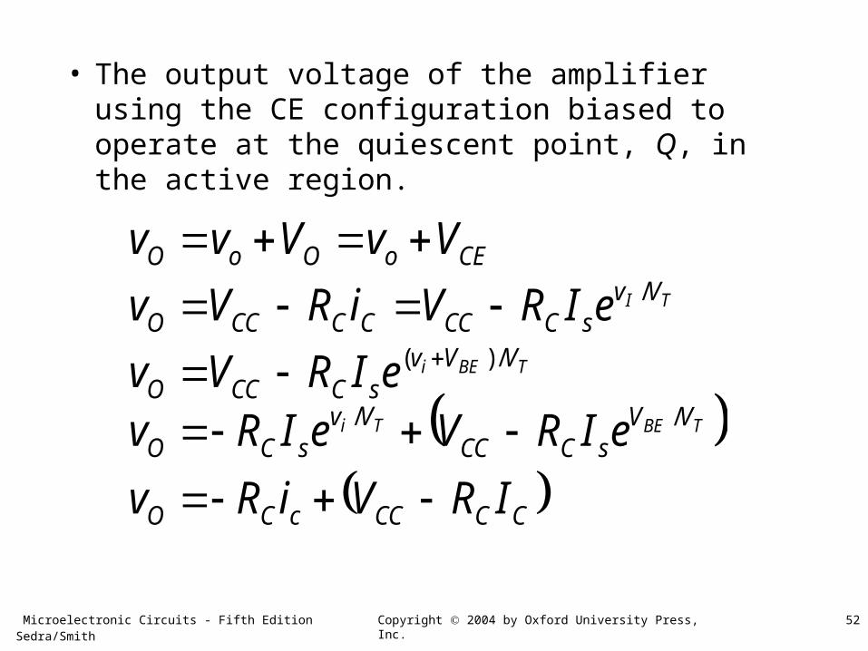
• The output voltage of the amplifier using the CE configuration biased to operate at the quiescent point, Q, in the active region.
CCCCcCO
VVsCCC
VvsCO
VVvsCCCO
VvsCCCCCCCO
CEoOoO
IRViRv
eIRVeIRveIRVv
eIRViRVv
VvVvv
TBETi
TBEi
TI
//
/)(
/
Microelectronic Circuits - Fifth Edition Sedra/Smith 53Copyright 2004 by Oxford University Press, Inc.
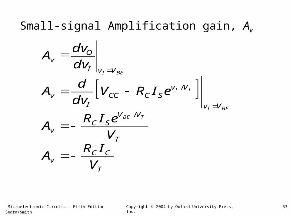
Small-signal Amplification gain, Av
T
CCv
T
VVSC
v
Vv
VvSCCC
Iv
VvI
Ov
V
IRA
V
eIRA
eIRVdv
dA
dv
dvA
TBE
BEI
TI
BEI
/
/

Microelectronic Circuits - Fifth Edition Sedra/Smith 54Copyright 2004 by Oxford University Press, Inc.
Figure 5.27 Circuit whose operation is to be analyzed graphically.

Microelectronic Circuits - Fifth Edition Sedra/Smith 55Copyright 2004 by Oxford University Press, Inc.
Figure 5.28 Graphical construction for the determination of the dc base current in the circuit of Fig. 5.27.

Microelectronic Circuits - Fifth Edition Sedra/Smith 56Copyright 2004 by Oxford University Press, Inc.
Figure 5.29 Graphical construction for determining the dc collector current IC and the collector-to-emitter voltage VCE in the circuit of Fig. 5.27.

Microelectronic Circuits - Fifth Edition Sedra/Smith 57Copyright 2004 by Oxford University Press, Inc.
Figure 5.30 Graphical determination of the signal components vbe, ib, ic, and vce when a signal component vi is superimposed on the dc voltage VBB (see Fig. 5.27).

Microelectronic Circuits - Fifth Edition Sedra/Smith 58Copyright 2004 by Oxford University Press, Inc.
Figure 5.31 Effect of bias-point location on allowable signal swing: Load-line A results in bias point QA with a corresponding VCE which is too close to VCC and thus limits the positive swing of vCE. At the other extreme, load-line B results in an operating point too close to the saturation region, thus limiting the negative swing of vCE.
Microelectronic Circuits - Fifth Edition Sedra/Smith 59Copyright 2004 by Oxford University Press, Inc.
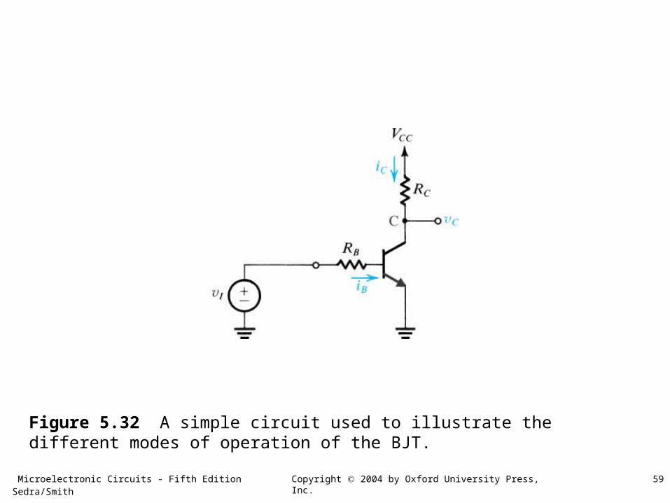
Figure 5.32 A simple circuit used to illustrate the different modes of operation of the BJT.
Microelectronic Circuits - Fifth Edition Sedra/Smith 60Copyright 2004 by Oxford University Press, Inc.
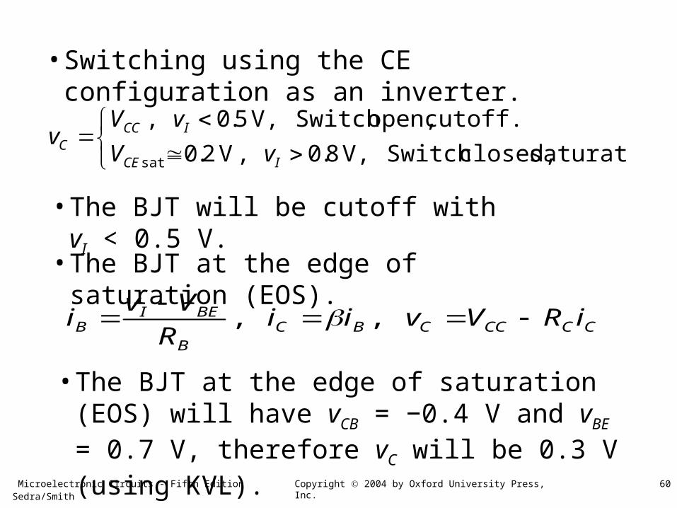
• Switching using the CE configuration as an inverter.
saturation closed,SwitchV,8.0,V2.0
cutoff.open,SwitchV,5.0,
sat ICE
ICCC vV
vVv
• The BJT will be cutoff with vI < 0.5 V.
• The BJT at the edge of saturation (EOS).
CCCCCBCB
BEIB iRVvii
R
Vvi
,,
• The BJT at the edge of saturation (EOS) will have vCB = −0.4 V and vBE = 0.7 V, therefore vC will be 0.3 V (using KVL).
Microelectronic Circuits - Fifth Edition Sedra/Smith 61Copyright 2004 by Oxford University Press, Inc.
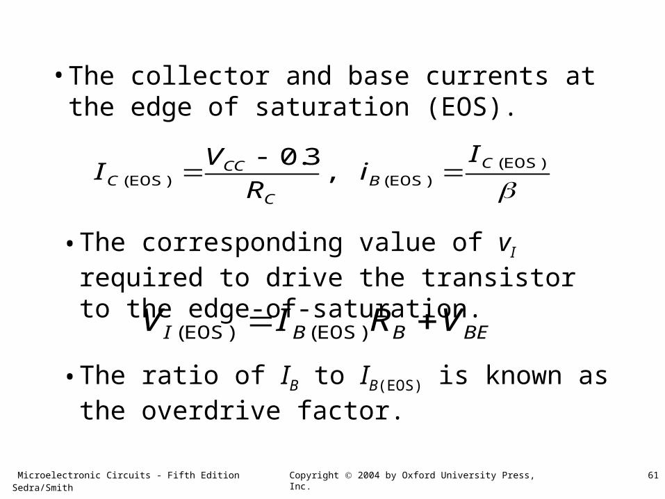
• The collector and base currents at the edge of saturation (EOS).
)EOS(
)EOS()EOS( ,3.0 C
BC
CCC
Ii
R
VI
• The corresponding value of vI required to drive the transistor to the edge-of-saturation.
BEBBI VRIV )EOS()EOS(
• The ratio of IB to IB(EOS) is known as the overdrive factor.

Microelectronic Circuits - Fifth Edition Sedra/Smith 62Copyright 2004 by Oxford University Press, Inc.
Figure 5.33 Circuit for Example 5.3.
Microelectronic Circuits - Fifth Edition Sedra/Smith 63Copyright 2004 by Oxford University Press, Inc.
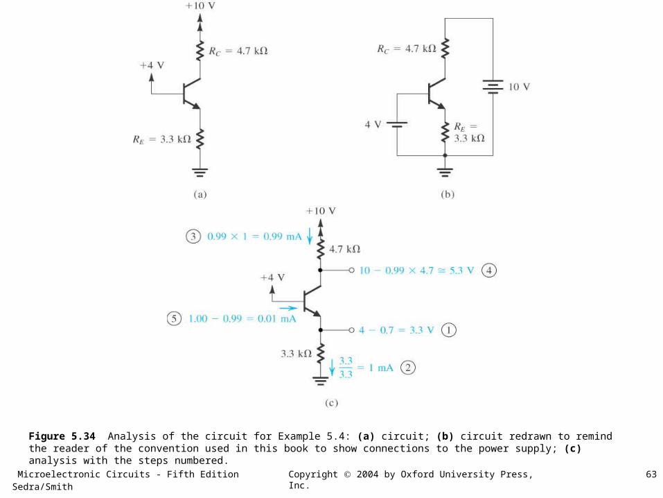
Figure 5.34 Analysis of the circuit for Example 5.4: (a) circuit; (b) circuit redrawn to remind the reader of the convention used in this book to show connections to the power supply; (c) analysis with the steps numbered.
Microelectronic Circuits - Fifth Edition Sedra/Smith 64Copyright 2004 by Oxford University Press, Inc.
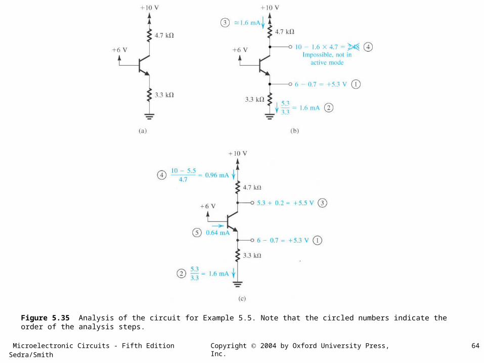
Figure 5.35 Analysis of the circuit for Example 5.5. Note that the circled numbers indicate the order of the analysis steps.

Microelectronic Circuits - Fifth Edition Sedra/Smith 65Copyright 2004 by Oxford University Press, Inc.
Figure 5.36 Example 5.6: (a) circuit; (b) analysis with the order of the analysis steps indicated by circled numbers.

Microelectronic Circuits - Fifth Edition Sedra/Smith 66Copyright 2004 by Oxford University Press, Inc.
Figure 5.37 Example 5.7: (a) circuit; (b) analysis with the steps indicated by circled numbers.

Microelectronic Circuits - Fifth Edition Sedra/Smith 67Copyright 2004 by Oxford University Press, Inc.
Figure 5.38 Example 5.8: (a) circuit; (b) analysis with the steps indicated by the circled numbers.
Microelectronic Circuits - Fifth Edition Sedra/Smith 68Copyright 2004 by Oxford University Press, Inc.
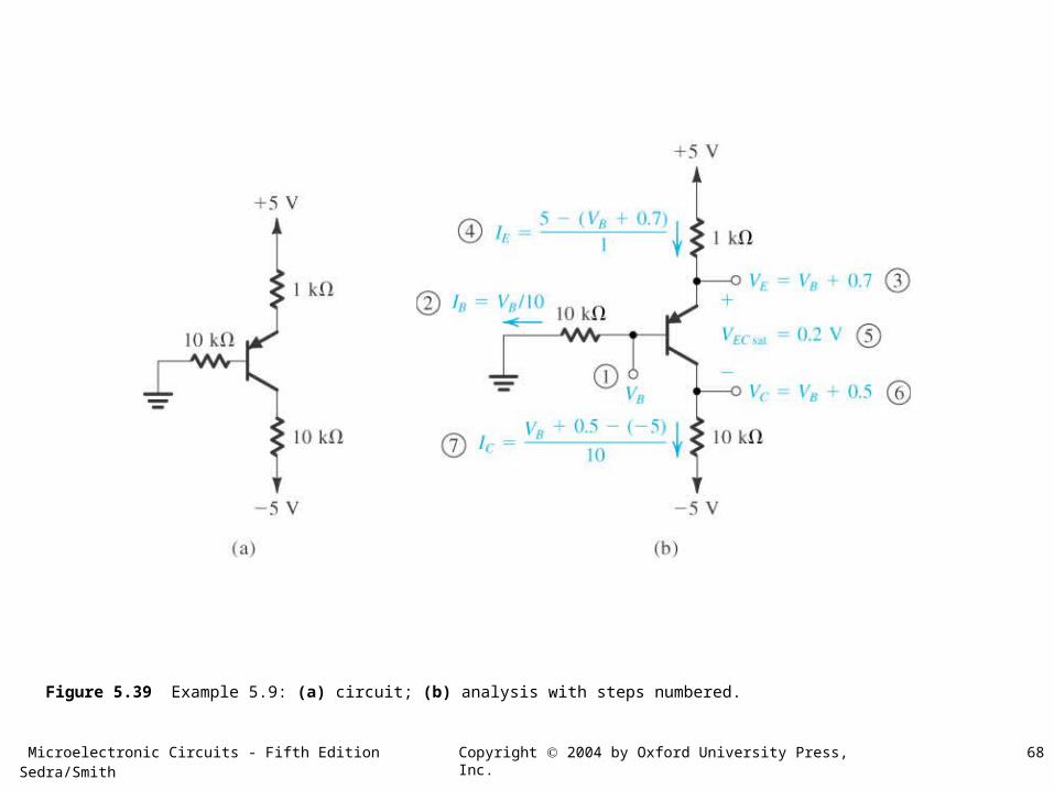
Figure 5.39 Example 5.9: (a) circuit; (b) analysis with steps numbered.

Microelectronic Circuits - Fifth Edition Sedra/Smith 69Copyright 2004 by Oxford University Press, Inc.
Figure 5.40 Circuits for Example 5.10.

Microelectronic Circuits - Fifth Edition Sedra/Smith 70Copyright 2004 by Oxford University Press, Inc.
Figure 5.41 Circuits for Example 5.11.

Microelectronic Circuits - Fifth Edition Sedra/Smith 71Copyright 2004 by Oxford University Press, Inc.
Figure E5.30
Microelectronic Circuits - Fifth Edition Sedra/Smith 72Copyright 2004 by Oxford University Press, Inc.
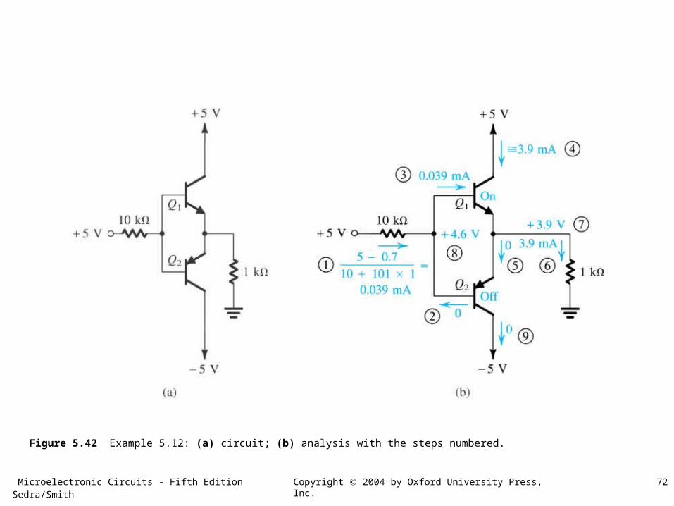
Figure 5.42 Example 5.12: (a) circuit; (b) analysis with the steps numbered.

Microelectronic Circuits - Fifth Edition Sedra/Smith 73Copyright 2004 by Oxford University Press, Inc.
Figure 5.43 Two obvious schemes for biasing the BJT: (a) by fixing VBE; (b) by fixing IB. Both result in wide variations in IC and hence in VCE and therefore are considered to be “bad.” Neither scheme is recommended.

Microelectronic Circuits - Fifth Edition Sedra/Smith 74Copyright 2004 by Oxford University Press, Inc.
Figure 5.44 Classical biasing for BJTs using a single power supply: (a) circuit; (b) circuit with the voltage divider supplying the base replaced with its Thévenin equivalent.

Microelectronic Circuits - Fifth Edition Sedra/Smith 75Copyright 2004 by Oxford University Press, Inc.
Figure 5.45 Biasing the BJT using two power supplies. Resistor RB is needed only if the signal is to be capacitively coupled to the base. Otherwise, the base can be connected directly to ground, or to a grounded signal source, resulting in almost total -independence of the bias current.

Microelectronic Circuits - Fifth Edition Sedra/Smith 76Copyright 2004 by Oxford University Press, Inc.
Figure 5.46 (a) A common-emitter transistor amplifier biased by a feedback resistor RB. (b) Analysis of the circuit in (a).
Microelectronic Circuits - Fifth Edition Sedra/Smith 77Copyright 2004 by Oxford University Press, Inc.
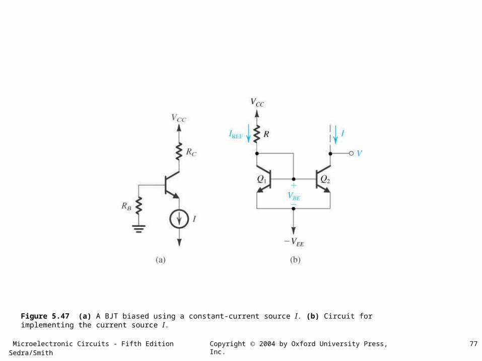
Figure 5.47 (a) A BJT biased using a constant-current source I. (b) Circuit for implementing the current source I.
Microelectronic Circuits - Fifth Edition Sedra/Smith 78Copyright 2004 by Oxford University Press, Inc.
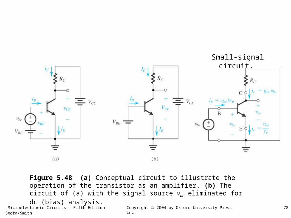
Figure 5.48 (a) Conceptual circuit to illustrate the operation of the transistor as an amplifier. (b) The circuit of (a) with the signal source vbe eliminated for dc (bias) analysis.
Small-signal circuit.
Microelectronic Circuits - Fifth Edition Sedra/Smith 79Copyright 2004 by Oxford University Press, Inc.
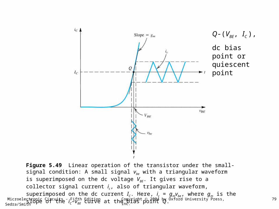
Figure 5.49 Linear operation of the transistor under the small-signal condition: A small signal vbe with a triangular waveform is superimposed on the dc voltage VBE. It gives rise to a collector signal current ic, also of triangular waveform, superimposed on the dc current IC. Here, ic = gmvbe, where gm is the slope of the iC–vBE curve at the bias point Q.
Q-(VBE, IC ),
dc bias point or quiescent point
Microelectronic Circuits - Fifth Edition Sedra/Smith 80Copyright 2004 by Oxford University Press, Inc.
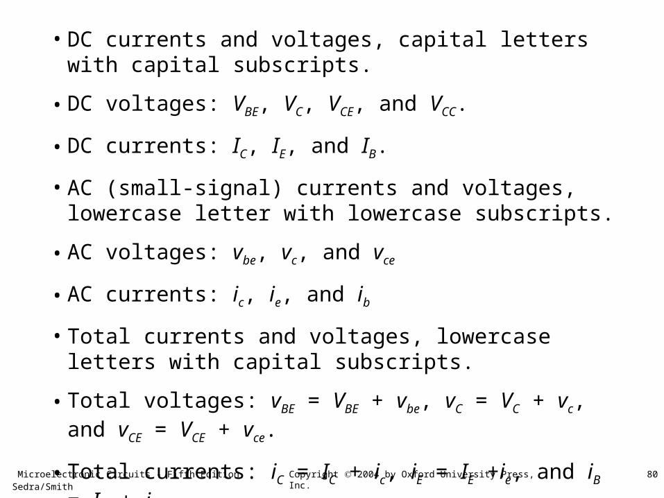
• DC currents and voltages, capital letters with capital subscripts.
• DC voltages: VBE, VC, VCE, and VCC.
• DC currents: IC, IE, and IB.
• AC (small-signal) currents and voltages, lowercase letter with lowercase subscripts.
• AC voltages: vbe, vc, and vce
• AC currents: ic, ie, and ib
• Total currents and voltages, lowercase letters with capital subscripts.
• Total voltages: vBE = VBE + vbe, vC = VC + vc, and vCE = VCE + vce.
• Total currents: iC = IC + ic, iE = IE +ie, and iB = IB + ib.
Microelectronic Circuits - Fifth Edition Sedra/Smith 81Copyright 2004 by Oxford University Press, Inc.
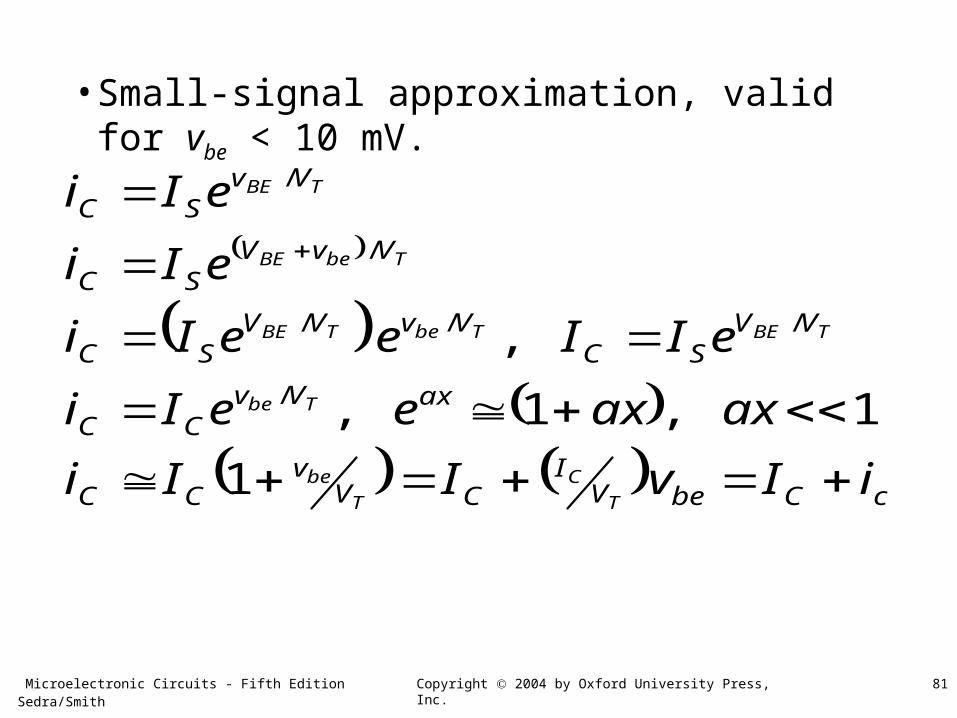
• Small-signal approximation, valid for vbe < 10 mV.
cCbeVI
CVv
CC
axVvCC
VVSC
VvVVSC
VvVSC
VvSC
iIvIIi
axaxeeIi
eIIeeIi
eIi
eIi
T
C
T
be
Tbe
TBETbeTBE
TbeBE
TBE
1
1,1,
,/
///
/
/
Microelectronic Circuits - Fifth Edition Sedra/Smith 82Copyright 2004 by Oxford University Press, Inc.
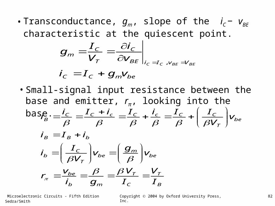
• Transconductance, gm, slope of the iC − vBE characteristic at the quiescent point.
bemCC
VvIiBE
C
T
Cm
vgIi
v
i
V
Ig
BEBECC
,
• Small-signal input resistance between the base and emitter, rπ, looking into the base.
B
T
C
T
mb
be
bem
beT
Cb
bBB
beT
CCcCcCCB
I
V
I
V
gi
vr
vg
vV
Ii
iIi
vV
IIiIiIii

Microelectronic Circuits - Fifth Edition Sedra/Smith 83Copyright 2004 by Oxford University Press, Inc.
• Small-signal resistance between base and emitter, looking into the emitter, re.
mE
T
C
T
me
bee
bem
beT
Ce
eEE
beT
CCcCcCCE
gI
V
I
V
gi
vr
vg
vV
Ii
iIi
vV
IIiIiIii
1
• Relationship between re and rπ
eeb
e
eebbe
rri
ir
ririv
1
Microelectronic Circuits - Fifth Edition Sedra/Smith 84Copyright 2004 by Oxford University Press, Inc.
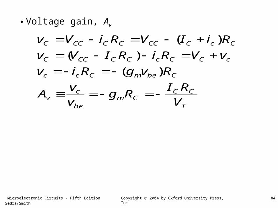
• Voltage gain, Av
T
CCCm
be
cv
CbemCcc
cCCcCCCCC
CcCCCCCCCC
V
RIRg
v
vA
RvgRiv
vVRiRIVv
RiIVRiVv
)(
)(
)(

Microelectronic Circuits - Fifth Edition Sedra/Smith 85Copyright 2004 by Oxford University Press, Inc.
Figure 5.50 The amplifier circuit of Fig. 5.48(a) with the dc sources (VBE and VCC) eliminated (short circuited). Thus only the signal components are present. Note that this is a representation of the signal operation of the BJT and not an actual amplifier circuit.
Microelectronic Circuits - Fifth Edition Sedra/Smith 86Copyright 2004 by Oxford University Press, Inc.
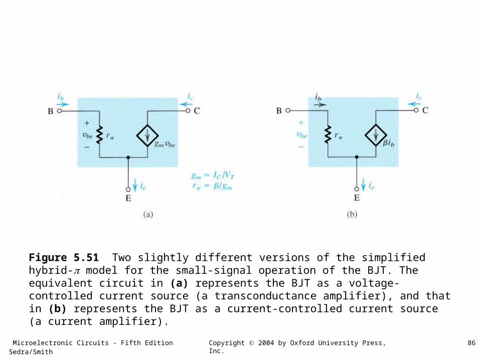
Figure 5.51 Two slightly different versions of the simplified hybrid- model for the small-signal operation of the BJT. The equivalent circuit in (a) represents the BJT as a voltage-controlled current source (a transconductance amplifier), and that in (b) represents the BJT as a current-controlled current source (a current amplifier).
Microelectronic Circuits - Fifth Edition Sedra/Smith 87Copyright 2004 by Oxford University Press, Inc.
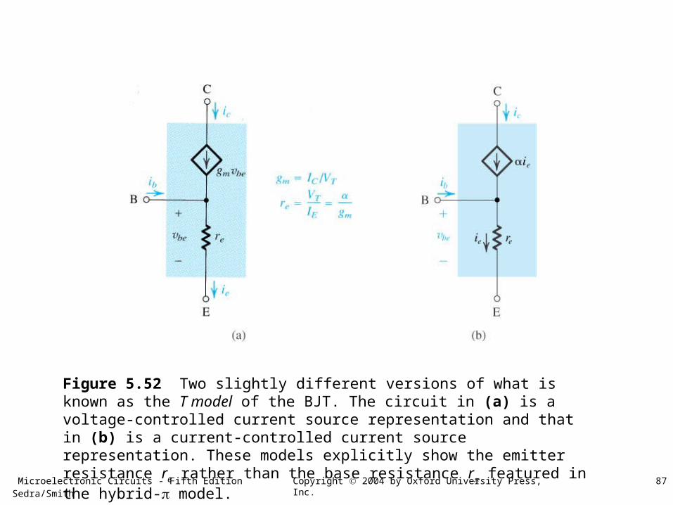
Figure 5.52 Two slightly different versions of what is known as the T model of the BJT. The circuit in (a) is a voltage-controlled current source representation and that in (b) is a current-controlled current source representation. These models explicitly show the emitter resistance re rather than the base resistance r featured in the hybrid- model.
Microelectronic Circuits - Fifth Edition Sedra/Smith 88Copyright 2004 by Oxford University Press, Inc.
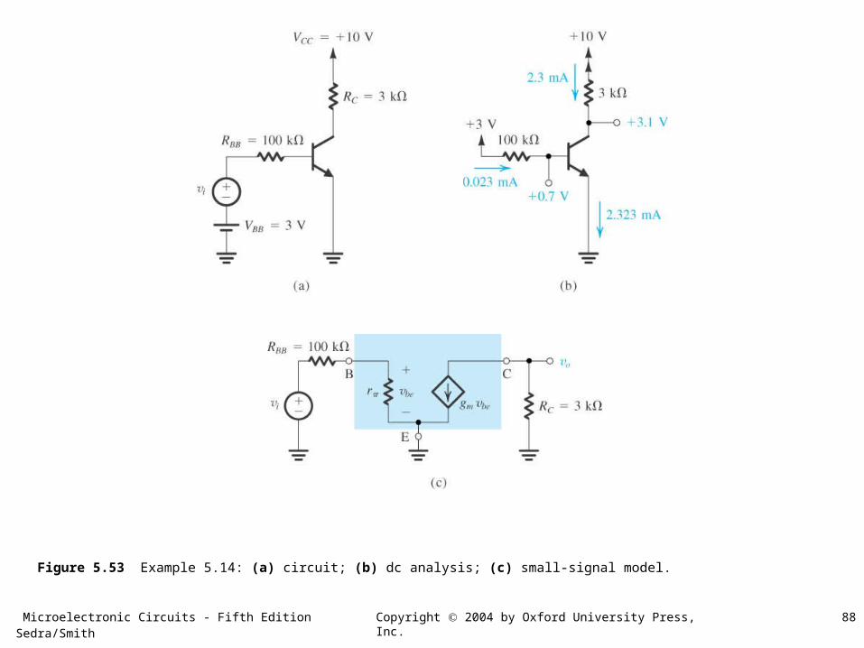
Figure 5.53 Example 5.14: (a) circuit; (b) dc analysis; (c) small-signal model.
Microelectronic Circuits - Fifth Edition Sedra/Smith 89Copyright 2004 by Oxford University Press, Inc.
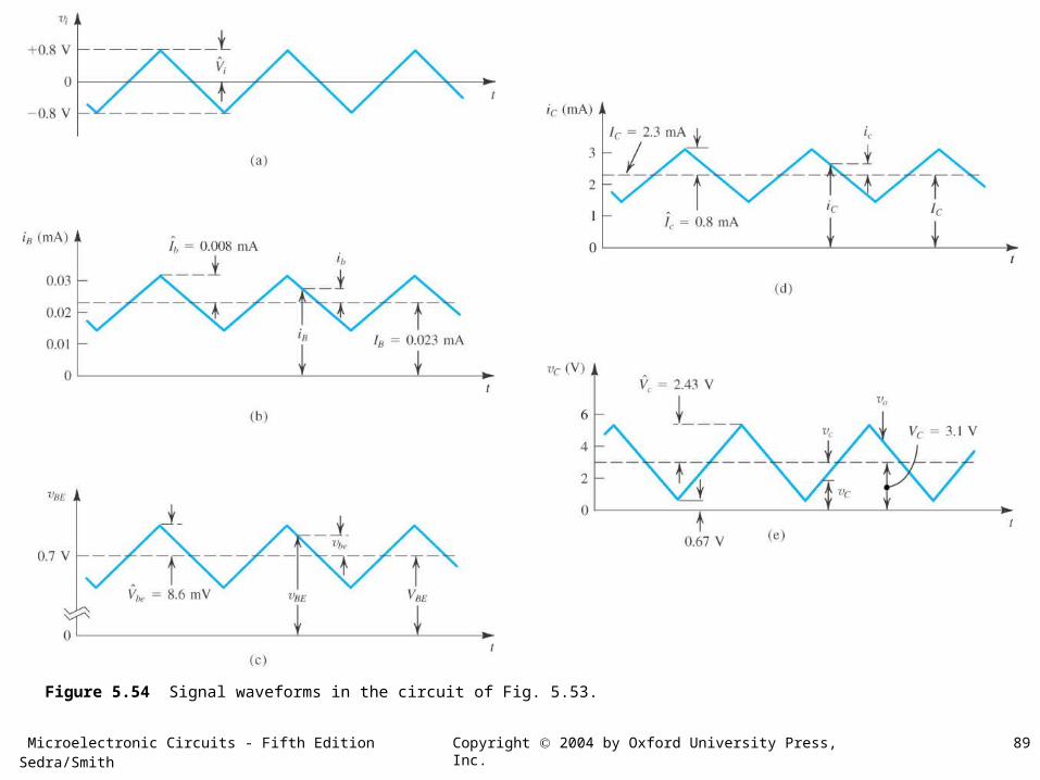
Figure 5.54 Signal waveforms in the circuit of Fig. 5.53.

Microelectronic Circuits - Fifth Edition Sedra/Smith 90Copyright 2004 by Oxford University Press, Inc.
Figure 5.55 Example 5.16: (a) circuit; (b) dc analysis; (c) small-signal model; (d) small-signal analysis performed directly on the circuit.
Microelectronic Circuits - Fifth Edition Sedra/Smith 91Copyright 2004 by Oxford University Press, Inc.
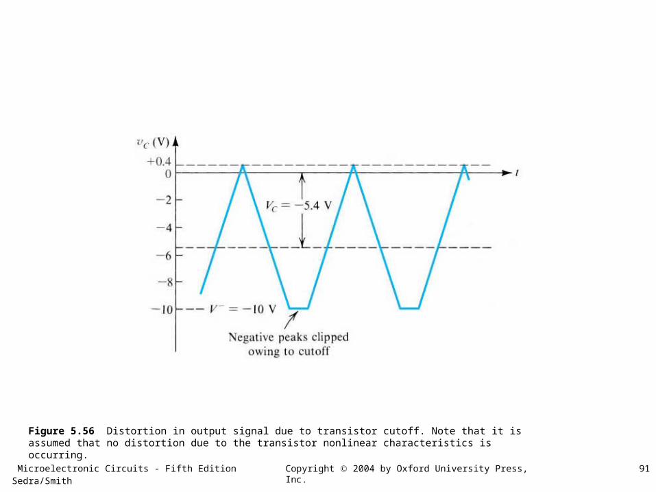
Figure 5.56 Distortion in output signal due to transistor cutoff. Note that it is assumed that no distortion due to the transistor nonlinear characteristics is occurring.

Microelectronic Circuits - Fifth Edition Sedra/Smith 92Copyright 2004 by Oxford University Press, Inc.
Figure 5.57 Input and output waveforms for the circuit of Fig. 5.55. Observe that this amplifier is noninverting, a property of the common-base configuration.
Microelectronic Circuits - Fifth Edition Sedra/Smith 93Copyright 2004 by Oxford University Press, Inc.
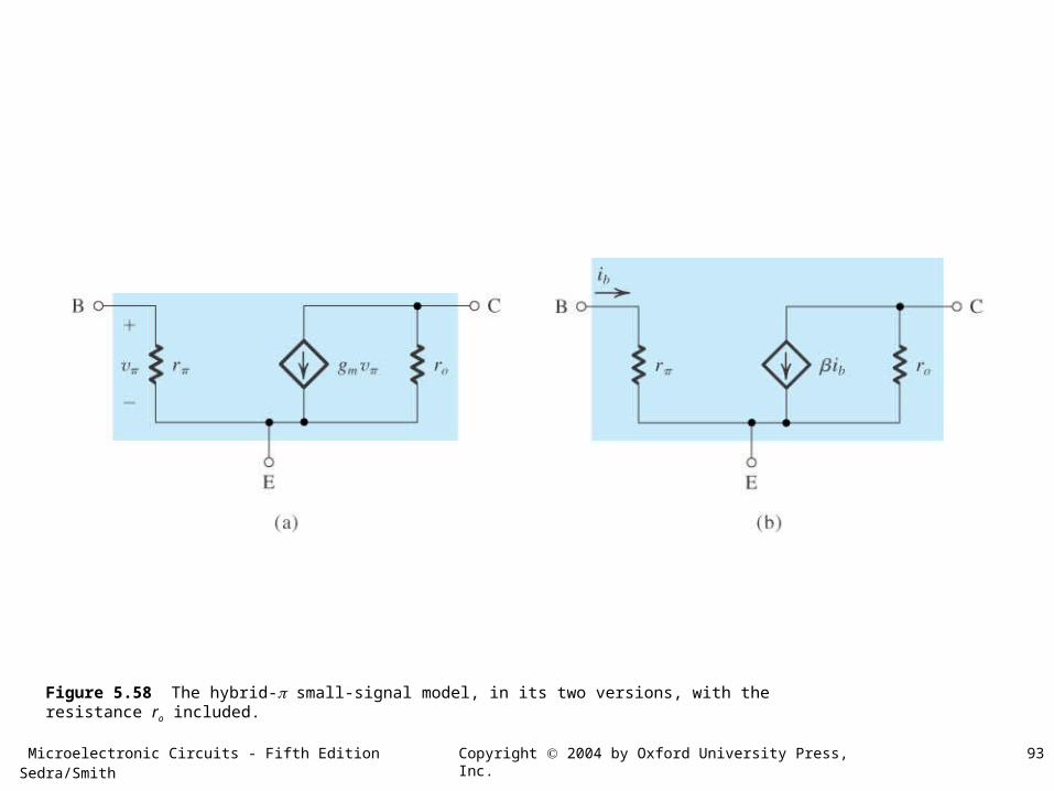
Figure 5.58 The hybrid- small-signal model, in its two versions, with the resistance ro included.

Microelectronic Circuits - Fifth Edition Sedra/Smith 94Copyright 2004 by Oxford University Press, Inc.
Figure E5.40

Microelectronic Circuits - Fifth Edition Sedra/Smith 95Copyright 2004 by Oxford University Press, Inc.
Table 5.4
Microelectronic Circuits - Fifth Edition Sedra/Smith 96Copyright 2004 by Oxford University Press, Inc.
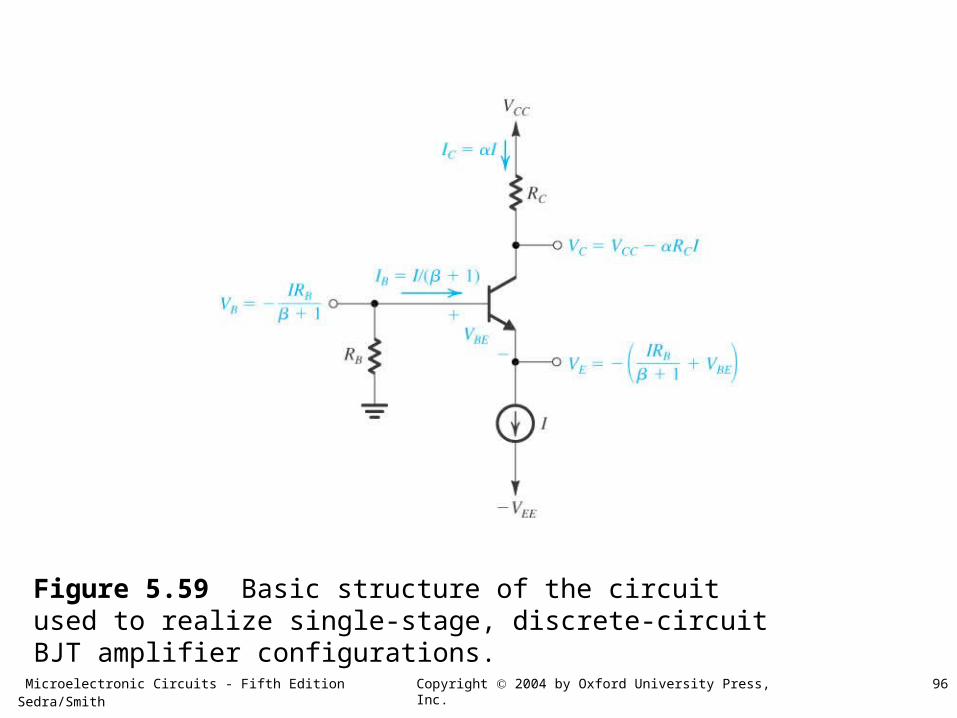
Figure 5.59 Basic structure of the circuit used to realize single-stage, discrete-circuit BJT amplifier configurations.

Microelectronic Circuits - Fifth Edition Sedra/Smith 97Copyright 2004 by Oxford University Press, Inc.
Figure E5.41

Microelectronic Circuits - Fifth Edition Sedra/Smith 98Copyright 2004 by Oxford University Press, Inc.
Table 5.5
Microelectronic Circuits - Fifth Edition Sedra/Smith 99Copyright 2004 by Oxford University Press, Inc.
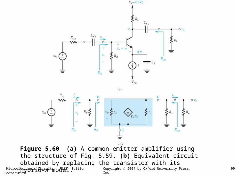
Figure 5.60 (a) A common-emitter amplifier using the structure of Fig. 5.59. (b) Equivalent circuit obtained by replacing the transistor with its hybrid- model.
Microelectronic Circuits - Fifth Edition Sedra/Smith 100Copyright 2004 by Oxford University Press, Inc.
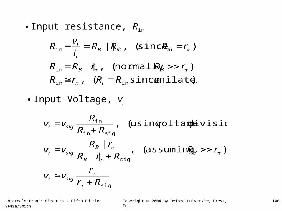
)unilateralsince(,
)normally(,||
)since(,||
inin
in
in
RRrR
rRrRR
rRRRi
vR
i
BB
ibibBi
i
• Input resistance, Rin
• Input Voltage, vi
sig
sig
sigin
in
)assuming(,||
||
division)voltageusing(,
Rr
rvv
rRRrR
rRvv
RR
Rvv
sigi
BB
Bsigi
sigi
Microelectronic Circuits - Fifth Edition Sedra/Smith 101Copyright 2004 by Oxford University Press, Inc.
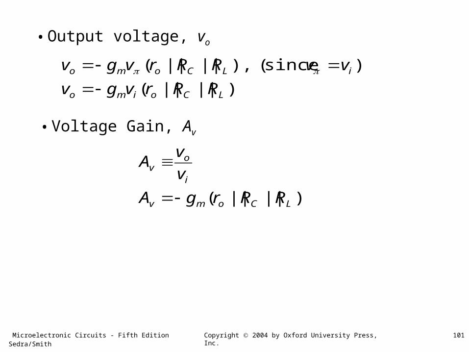
• Output voltage, vo
)||||(
)since(),||||(
LCoimo
iLComo
RRrvgv
vvRRrvgv
• Voltage Gain, Av
)||||( LComv
i
ov
RRrgA
v
vA

Microelectronic Circuits - Fifth Edition Sedra/Smith 102Copyright 2004 by Oxford University Press, Inc.
Cmvo
CoComvo
Comvo
Ri
ovo
RgA
RrtypicallyRrgA
RrgA
v
vA
L
)(),||(
)||||(
• Output resistance, Rout
• Open-circuit voltage Gain, Avo
),unilateralsince(,
)typically(,||
outoCout
CooCout
RRRR
RrrRR

Microelectronic Circuits - Fifth Edition Sedra/Smith 103Copyright 2004 by Oxford University Press, Inc.
• Overall voltage gain, Gv
)casethefor(,)||||(
)||||(||
||
sig
sig
rR
Rr
RRrG
RRrgRrR
rRG
Av
v
v
v
v
v
v
vG
BLCo
v
LComB
Bv
vsig
i
i
o
sig
i
sig
ov

Microelectronic Circuits - Fifth Edition Sedra/Smith 104Copyright 2004 by Oxford University Press, Inc.
• Overall voltage gain, Gv, is highly dependent on β if Rsig >> r π, an undesirable property.
• If Rsig << rπ then the overall voltage gain is almost independent of β.
)(),||||( sig rRandrRrRRgG BoLCmv
Microelectronic Circuits - Fifth Edition Sedra/Smith 105Copyright 2004 by Oxford University Press, Inc.
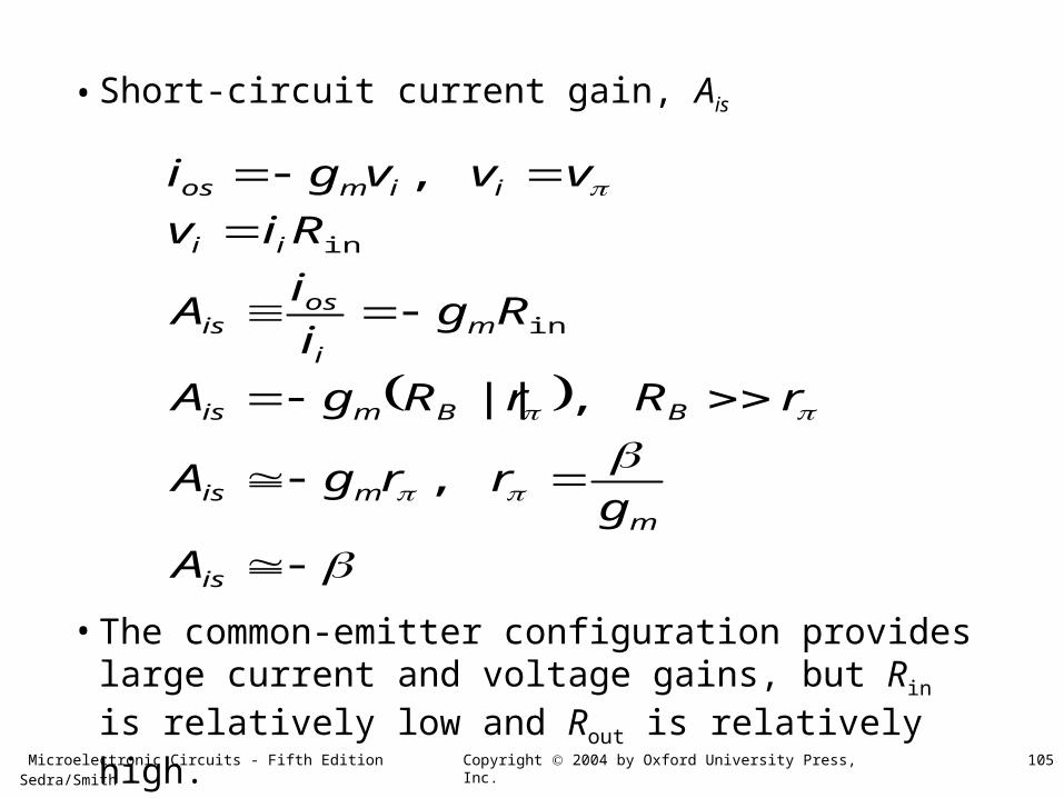
• Short-circuit current gain, Ais
is
mmis
BBmis
mi
osis
ii
iimos
A
grrgA
rRrRgA
Rgi
iA
Riv
vvvgi
,
,||
,
in
in
• The common-emitter configuration provides large current and voltage gains, but Rin is relatively low and Rout is relatively high.

Microelectronic Circuits - Fifth Edition Sedra/Smith 106Copyright 2004 by Oxford University Press, Inc.
Figure 5.61 (a) A common-emitter amplifier with an emitter resistance Re. (b) Equivalent circuit obtained by replacing the transistor with its T model.

Microelectronic Circuits - Fifth Edition Sedra/Smith 107Copyright 2004 by Oxford University Press, Inc.
• Input resistance, Rin
))(1(
1,
||in
eeib
ee
ie
eb
b
iib
ibBi
i
RrR
Rr
viand
iiwhere
i
vR
RRi
vR
• The input resistance looking into the base, Rib, is (β + 1) times the total resistance in the emitter. This is known as the resistance-reflection rule.
eme
e
e
ee
eib
eib
Rgr
Rr
Rr
RR
RR
11
)1(
))(1(
)without(
)includedwith(
Microelectronic Circuits - Fifth Edition Sedra/Smith 108Copyright 2004 by Oxford University Press, Inc.
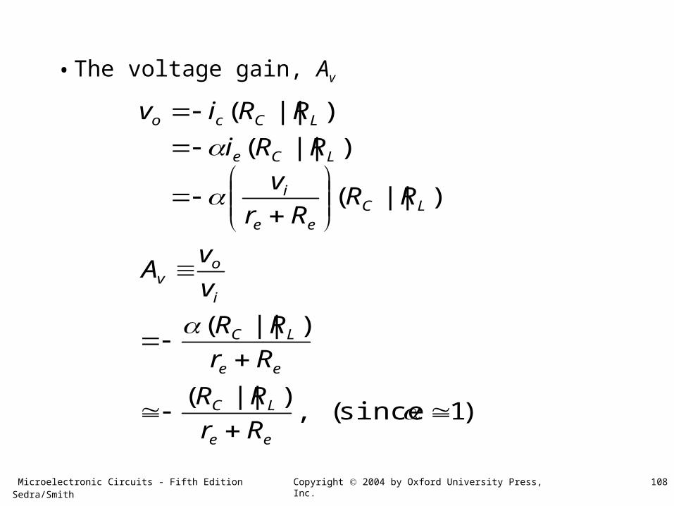
• The voltage gain, Av
)1since(,)||(
)||(
)||(
)||(
)||(
ee
LC
ee
LC
i
ov
LCee
i
LCe
LCco
Rr
RR
Rr
RR
v
vA
RRRr
v
RRi
RRiv
Microelectronic Circuits - Fifth Edition Sedra/Smith 109Copyright 2004 by Oxford University Press, Inc.
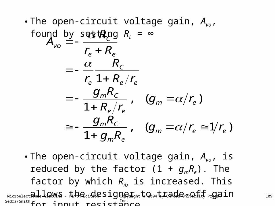
• The open-circuit voltage gain, Avo, found by setting RL = ∞
)1(,1
)(,1
1
eemem
Cm
emee
Cm
ee
C
e
ee
Cvo
rrgRg
Rg
rgrR
RgrR
R
r
Rr
RA
• The open-circuit voltage gain, Avo, is reduced by the factor (1 + gmRe). The factor by which Rib is increased. This allows the designer to trade-off gain for input resistance.
Microelectronic Circuits - Fifth Edition Sedra/Smith 110Copyright 2004 by Oxford University Press, Inc.
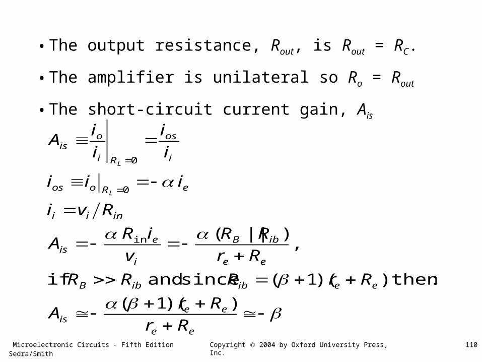
• The output resistance, Rout, is Rout = RC.
• The amplifier is unilateral so Ro = Rout
• The short-circuit current gain, Ais
ee
eeis
eeibibB
ee
ibB
i
eis
inii
eRoos
i
os
Ri
ois
Rr
RrA
RrRRR
Rr
RR
v
iRA
Rvi
iii
i
i
i
iA
L
L
))(1(
:then))(1(sinceandif
,)||(in
0
0
Microelectronic Circuits - Fifth Edition Sedra/Smith 111Copyright 2004 by Oxford University Press, Inc.
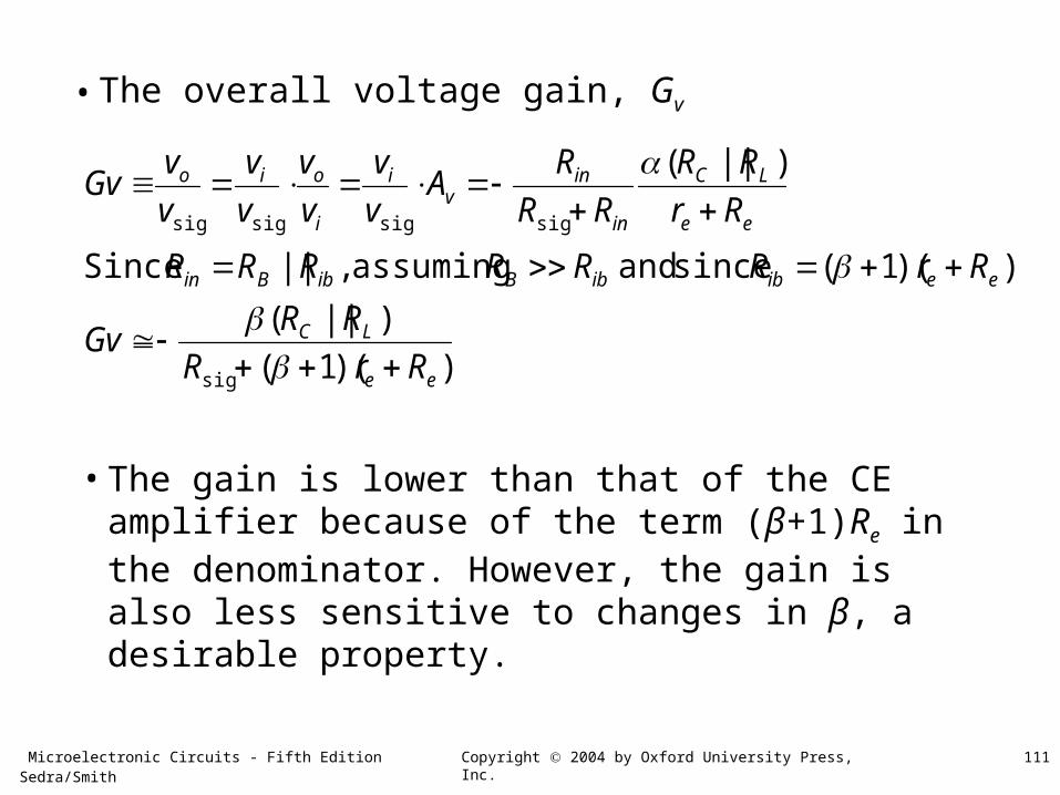
• The overall voltage gain, Gv
))(1(
)||(
))(1(sinceandassuming,||Since
)||(
sig
sigsigsigsig
ee
LC
eeibibBibBin
ee
LC
in
inv
i
i
oio
RrR
RRGv
RrRRRRRR
Rr
RR
RR
RA
v
v
v
v
v
v
v
vGv
• The gain is lower than that of the CE amplifier because of the term (β+1)Re in the denominator. However, the gain is also less sensitive to changes in β, a desirable property.
Microelectronic Circuits - Fifth Edition Sedra/Smith 112Copyright 2004 by Oxford University Press, Inc.
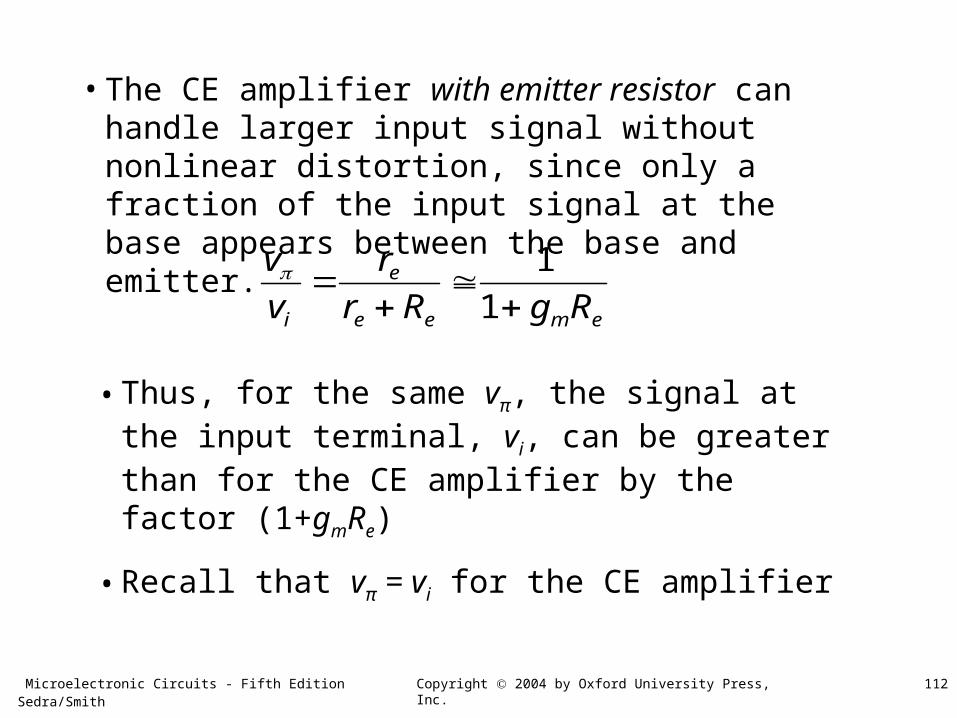
• The CE amplifier with emitter resistor can handle larger input signal without nonlinear distortion, since only a fraction of the input signal at the base appears between the base and emitter.
emee
e
i RgRr
r
v
v
1
1
• Thus, for the same vπ, the signal at the input terminal, vi, can be greater than for the CE amplifier by the factor (1+gmRe)
• Recall that vπ = vi for the CE amplifier

Microelectronic Circuits - Fifth Edition Sedra/Smith 113Copyright 2004 by Oxford University Press, Inc.
• The input resistance Rib is increased by the factor (1 + gmRe).
• The voltage gain from base to collector, Av, is reduced by the factor (1 + gmRe).
• For the same nonlinear distortion, the input signal vi can be increased by the factor (1 + gmRe).
• The overall voltage gain is less dependent on the value of β.
• The high-frequency response is significantly improved.
• The reduction in gain is the tradeoff for the other improvements.
Summary of the characteristics of the CE amplifier with emitter resistor.

Microelectronic Circuits - Fifth Edition Sedra/Smith 114Copyright 2004 by Oxford University Press, Inc.
Figure 5.62 (a) A common-base amplifier using the structure of Fig. 5.59. (b) Equivalent circuit obtained by replacing the transistor with its T model.
Microelectronic Circuits - Fifth Edition Sedra/Smith 115Copyright 2004 by Oxford University Press, Inc.
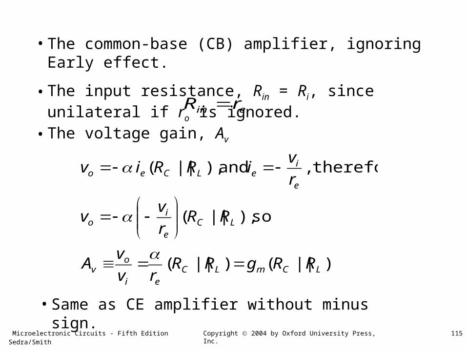
• The common-base (CB) amplifier, ignoring Early effect.
• The input resistance, Rin = Ri, since unilateral if ro is ignored.
ein rR
• The voltage gain, Av
)||()||(
so),||(
therefore,and),||(
LCmLCei
ov
LCe
io
e
ieLCeo
RRgRRrv
vA
RRr
vv
r
viRRiv
• Same as CE amplifier without minus sign.

Microelectronic Circuits - Fifth Edition Sedra/Smith 116Copyright 2004 by Oxford University Press, Inc.
• The output resistance, Rout = Ro, ignoring Early effect.
Cout RR
• The short-circuit current gain Ais.
e
e
i
eis i
i
i
iA
• The overall voltage gain, Gv.
e
LC
LCme
ev
i
i
oiov
e
ei
rR
RR
RRgrR
rA
v
v
v
v
v
v
v
vG
rR
r
v
v
sig
sigsigsigsig
sigsig
)||(
)||(
Microelectronic Circuits - Fifth Edition Sedra/Smith 117Copyright 2004 by Oxford University Press, Inc.
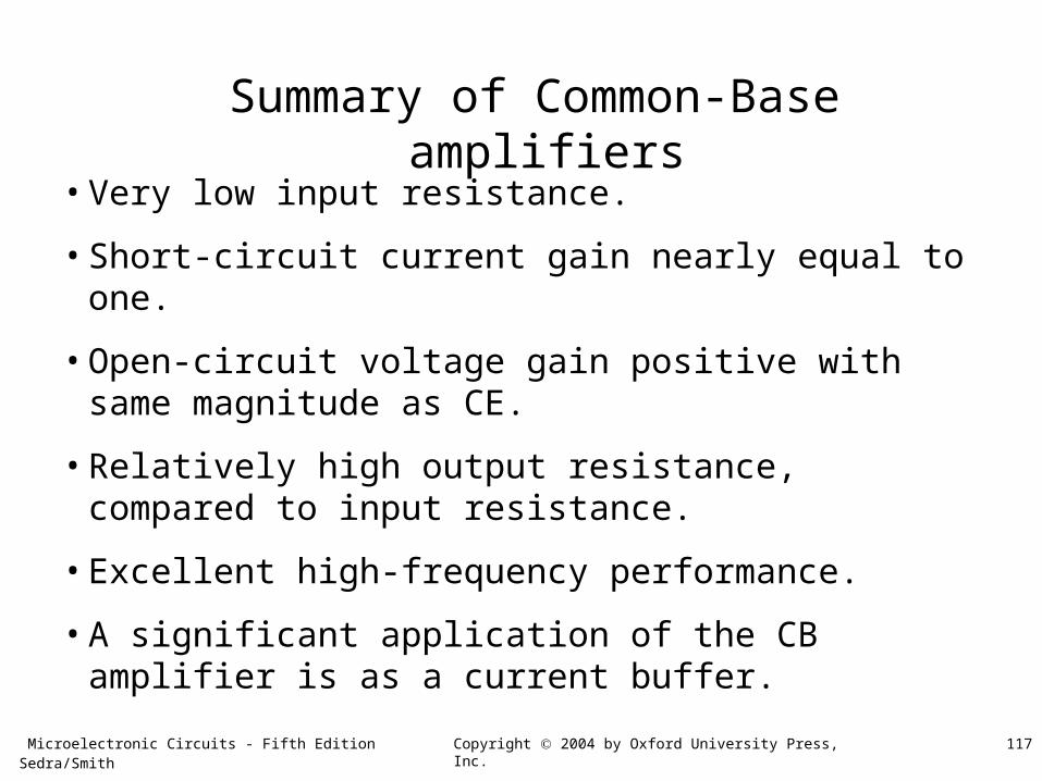
• Very low input resistance.
• Short-circuit current gain nearly equal to one.
• Open-circuit voltage gain positive with same magnitude as CE.
• Relatively high output resistance, compared to input resistance.
• Excellent high-frequency performance.
• A significant application of the CB amplifier is as a current buffer.
Summary of Common-Base amplifiers
Microelectronic Circuits - Fifth Edition Sedra/Smith 118Copyright 2004 by Oxford University Press, Inc.
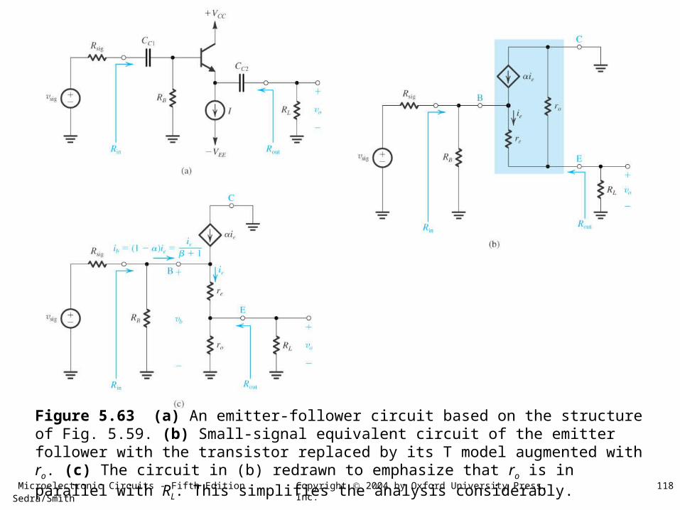
Figure 5.63 (a) An emitter-follower circuit based on the structure of Fig. 5.59. (b) Small-signal equivalent circuit of the emitter follower with the transistor replaced by its T model augmented with ro. (c) The circuit in (b) redrawn to emphasize that ro is in parallel with RL. This simplifies the analysis considerably.

Microelectronic Circuits - Fifth Edition Sedra/Smith 119Copyright 2004 by Oxford University Press, Inc.
Figure 5.64 (a) An equivalent circuit of the emitter follower obtained from the circuit in Fig. 5.63(c) by reflecting all resistances in the emitter to the base side. (b) The circuit in (a) after application of Thévenin theorem to the input circuit composed of vsig, Rsig, and RB.
Microelectronic Circuits - Fifth Edition Sedra/Smith 120Copyright 2004 by Oxford University Press, Inc.
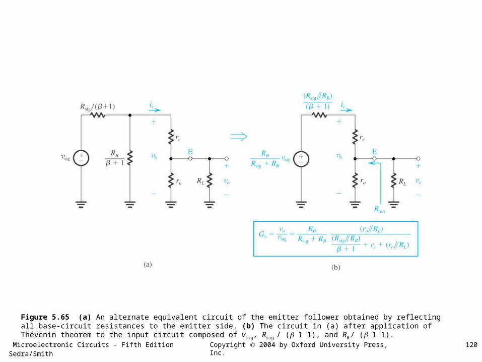
Figure 5.65 (a) An alternate equivalent circuit of the emitter follower obtained by reflecting all base-circuit resistances to the emitter side. (b) The circuit in (a) after application of Thévenin theorem to the input circuit composed of vsig, Rsig / ( 1 1), and RB / ( 1 1).
Microelectronic Circuits - Fifth Edition Sedra/Smith 121Copyright 2004 by Oxford University Press, Inc.
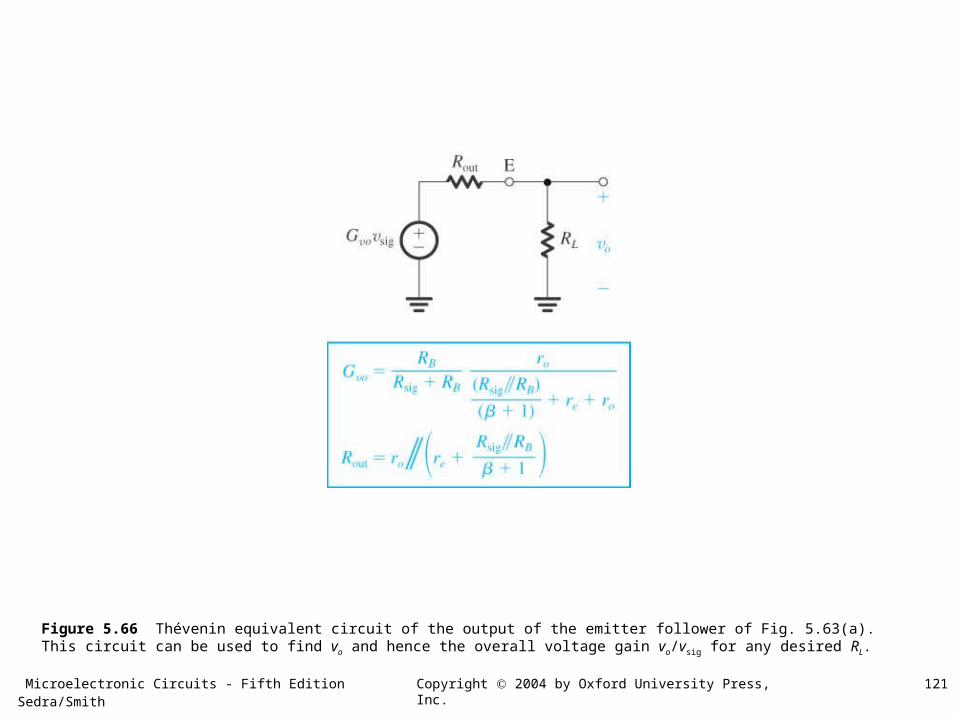
Figure 5.66 Thévenin equivalent circuit of the output of the emitter follower of Fig. 5.63(a). This circuit can be used to find vo and hence the overall voltage gain vo/vsig for any desired RL.

Microelectronic Circuits - Fifth Edition Sedra/Smith 122Copyright 2004 by Oxford University Press, Inc.
• The common-collector amplifier exhibits a high input resistance.
• The common-collector amplifier exhibits a low output resistance.
• The CC amplifier has a voltage gain smaller than, but very close to unity.
• The CC amplifier is often used as the last stage in a multi-stage amplifier (voltage buffer).
• The CC amplifier is also used to connect a high-resistance source to a low-resistance load.
Summary of the common-collector properties
Microelectronic Circuits - Fifth Edition Sedra/Smith 123Copyright 2004 by Oxford University Press, Inc.
Summary and Comparisons• The CE configuration is the best suited for realizing
the bulk of the gain required in an amplifier.• Including a resistor in the emitter lead of the CE
amplifier provides a number of performance improvements at the expense of gain reduction.
• The low input resistance of the CB amplifier makes it useful only in specific applications, such as high-frequency applications and as a current buffer.
• The CC is used as a voltage buffer for connecting a high-resistance source to a low-resistance load and as the output stage in a multistage amplifier.

Microelectronic Circuits - Fifth Edition Sedra/Smith 124Copyright 2004 by Oxford University Press, Inc.
Table 5.6
Microelectronic Circuits - Fifth Edition Sedra/Smith 125Copyright 2004 by Oxford University Press, Inc.
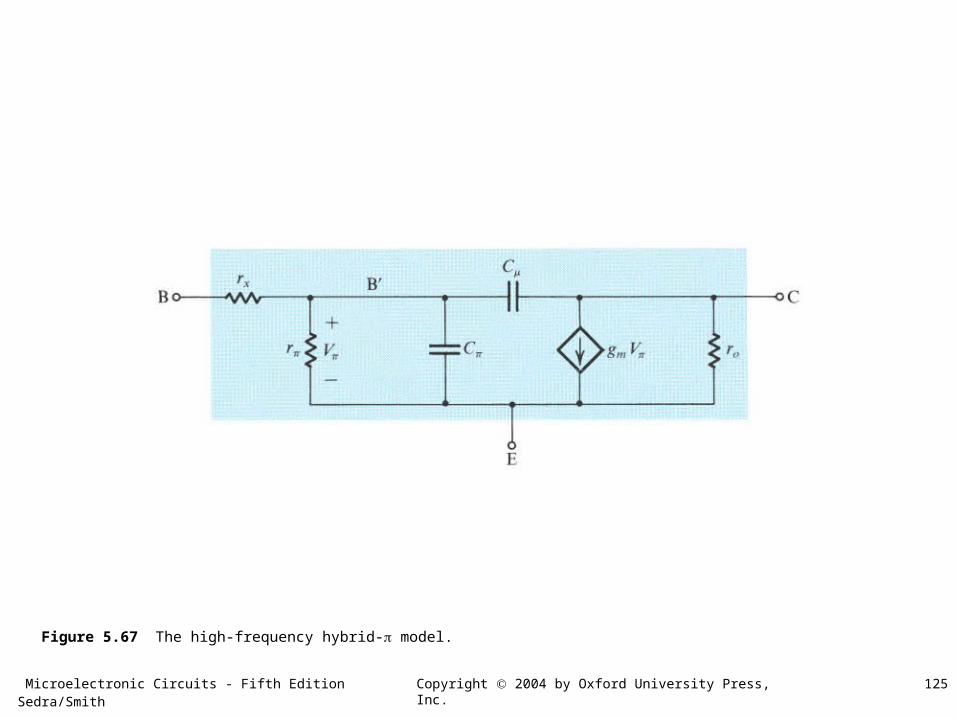
Figure 5.67 The high-frequency hybrid- model.

Microelectronic Circuits - Fifth Edition Sedra/Smith 126Copyright 2004 by Oxford University Press, Inc.
Figure 5.68 Circuit for deriving an expression for hfe(s) ; Ic/Ib.

Microelectronic Circuits - Fifth Edition Sedra/Smith 127Copyright 2004 by Oxford University Press, Inc.
Figure 5.69 Bode plot for uhfeu.

Microelectronic Circuits - Fifth Edition Sedra/Smith 128Copyright 2004 by Oxford University Press, Inc.
Figure 5.70 Variation of fT with IC.
Microelectronic Circuits - Fifth Edition Sedra/Smith 129Copyright 2004 by Oxford University Press, Inc.
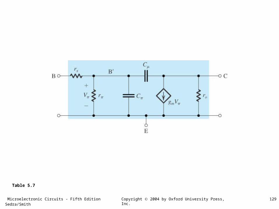
Table 5.7
Microelectronic Circuits - Fifth Edition Sedra/Smith 130Copyright 2004 by Oxford University Press, Inc.
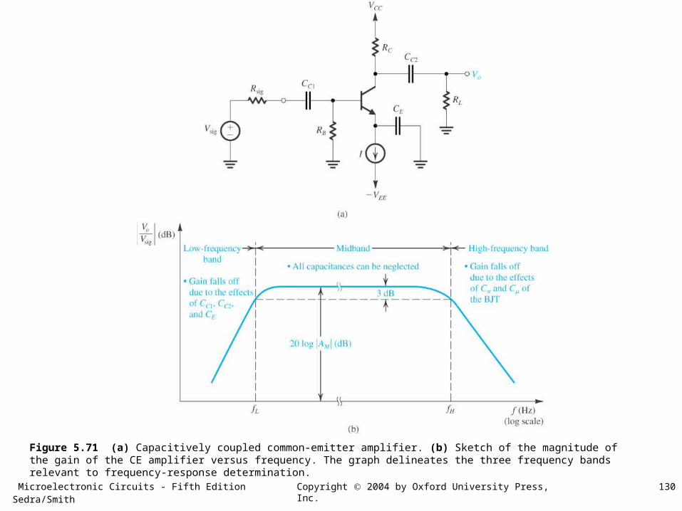
Figure 5.71 (a) Capacitively coupled common-emitter amplifier. (b) Sketch of the magnitude of the gain of the CE amplifier versus frequency. The graph delineates the three frequency bands relevant to frequency-response determination.
Microelectronic Circuits - Fifth Edition Sedra/Smith 131Copyright 2004 by Oxford University Press, Inc.
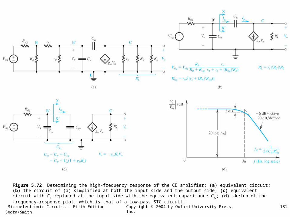
Figure 5.72 Determining the high-frequency response of the CE amplifier: (a) equivalent circuit; (b) the circuit of (a) simplified at both the input side and the output side; (c) equivalent circuit with C replaced at the input side with the equivalent capacitance Ceq; (d) sketch of the frequency-response plot, which is that of a low-pass STC circuit.

Microelectronic Circuits - Fifth Edition Sedra/Smith 132Copyright 2004 by Oxford University Press, Inc.
Figure 5.73 Analysis of the low-frequency response of the CE amplifier: (a) amplifier circuit with dc sources removed; (b) the effect of CC1 is determined with CE and CC2 assumed to be acting as perfect short circuits;
Microelectronic Circuits - Fifth Edition Sedra/Smith 133Copyright 2004 by Oxford University Press, Inc.
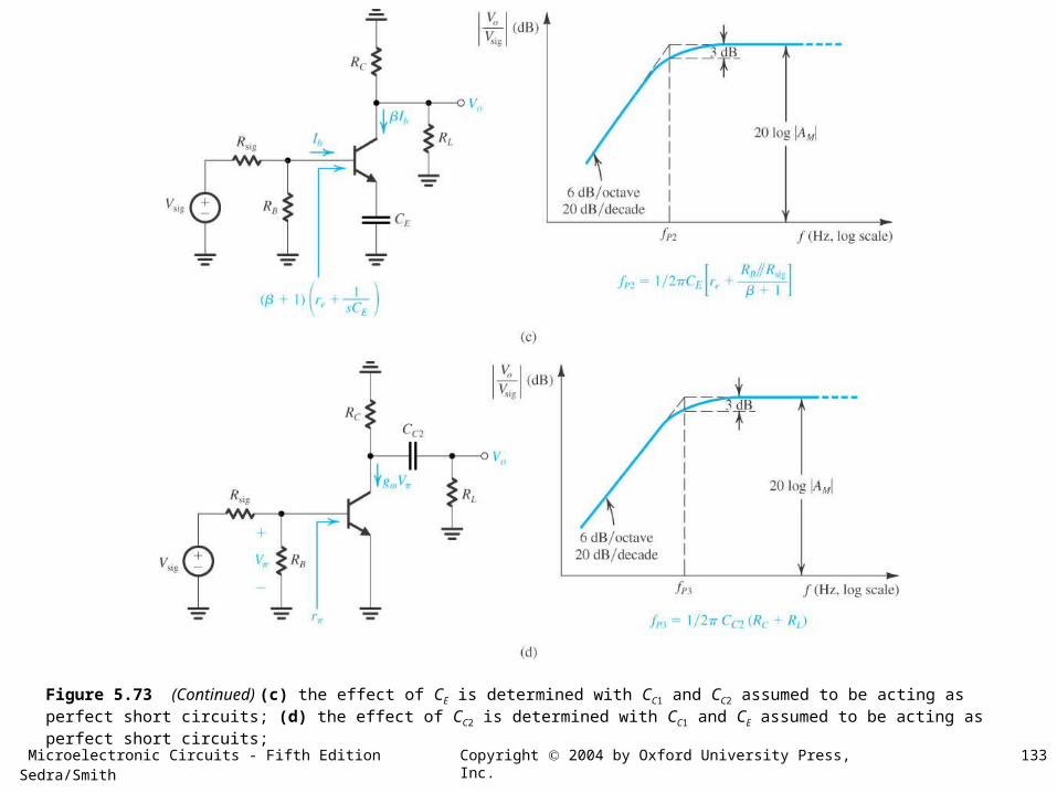
Figure 5.73 (Continued) (c) the effect of CE is determined with CC1 and CC2 assumed to be acting as perfect short circuits; (d) the effect of CC2 is determined with CC1 and CE assumed to be acting as perfect short circuits;

Microelectronic Circuits - Fifth Edition Sedra/Smith 134Copyright 2004 by Oxford University Press, Inc.
Figure 5.73 (Continued) (e) sketch of the low-frequency gain under the assumptions that CC1, CE, and CC2 do not interact and that their break (or pole) frequencies are widely separated.
Microelectronic Circuits - Fifth Edition Sedra/Smith 135Copyright 2004 by Oxford University Press, Inc.
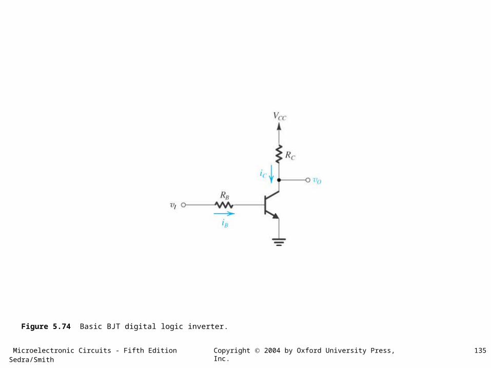
Figure 5.74 Basic BJT digital logic inverter.
Microelectronic Circuits - Fifth Edition Sedra/Smith 136Copyright 2004 by Oxford University Press, Inc.
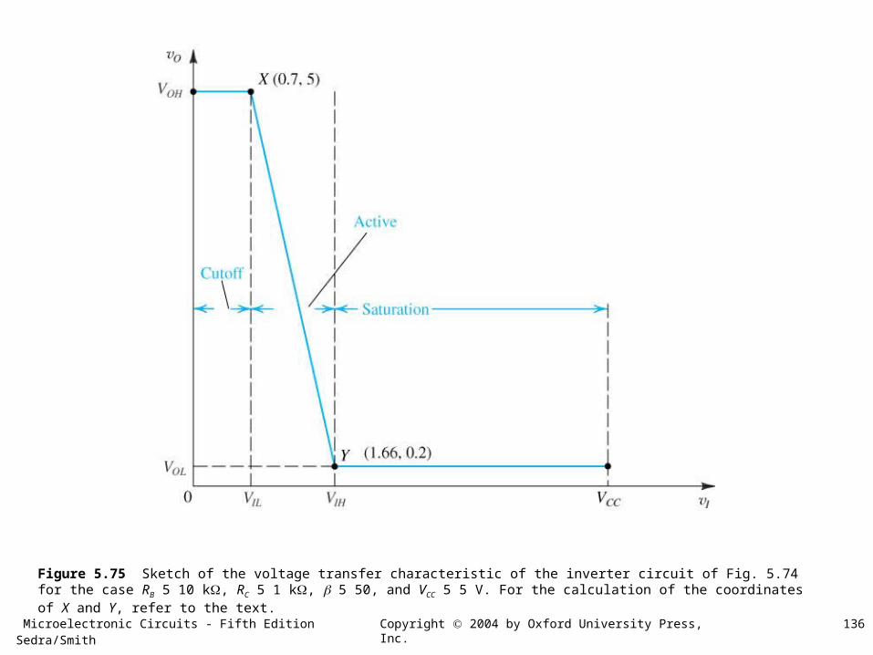
Figure 5.75 Sketch of the voltage transfer characteristic of the inverter circuit of Fig. 5.74 for the case RB 5 10 k, RC 5 1 k, 5 50, and VCC 5 5 V. For the calculation of the coordinates of X and Y, refer to the text.
Microelectronic Circuits - Fifth Edition Sedra/Smith 137Copyright 2004 by Oxford University Press, Inc.
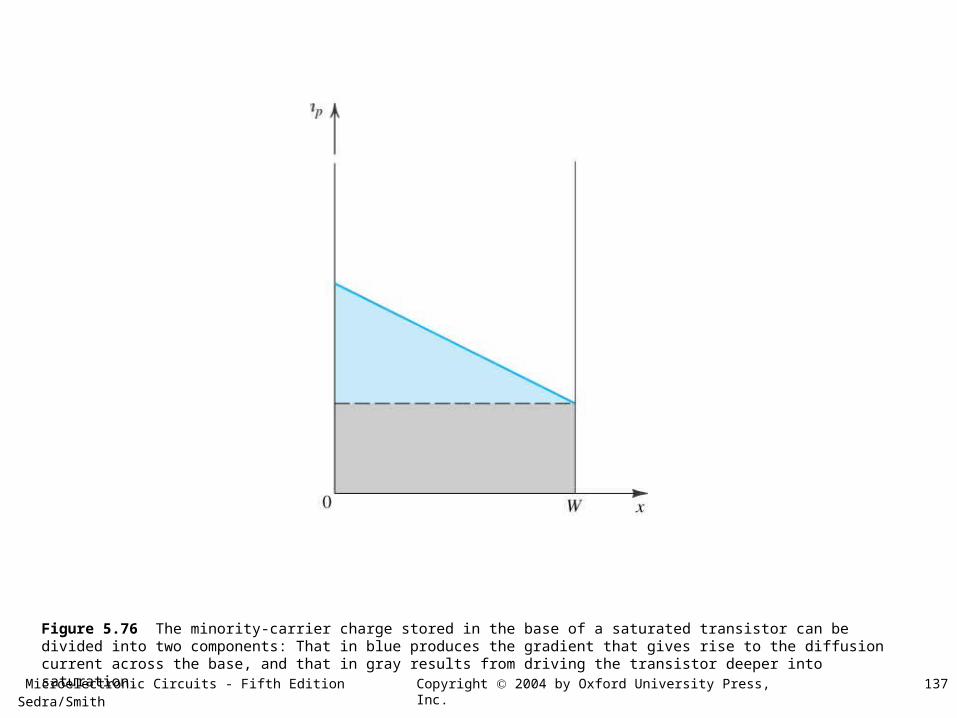
Figure 5.76 The minority-carrier charge stored in the base of a saturated transistor can be divided into two components: That in blue produces the gradient that gives rise to the diffusion current across the base, and that in gray results from driving the transistor deeper into saturation.

Microelectronic Circuits - Fifth Edition Sedra/Smith 138Copyright 2004 by Oxford University Press, Inc.
Figure E5.53
Microelectronic Circuits - Fifth Edition Sedra/Smith 139Copyright 2004 by Oxford University Press, Inc.
Figure 5.77 The transport form of the Ebers-Moll model for an npn BJT.

Microelectronic Circuits - Fifth Edition Sedra/Smith 140Copyright 2004 by Oxford University Press, Inc.
Figure 5.78 The SPICE large-signal Ebers-Moll model for an npn BJT.
Microelectronic Circuits - Fifth Edition Sedra/Smith 141Copyright 2004 by Oxford University Press, Inc.
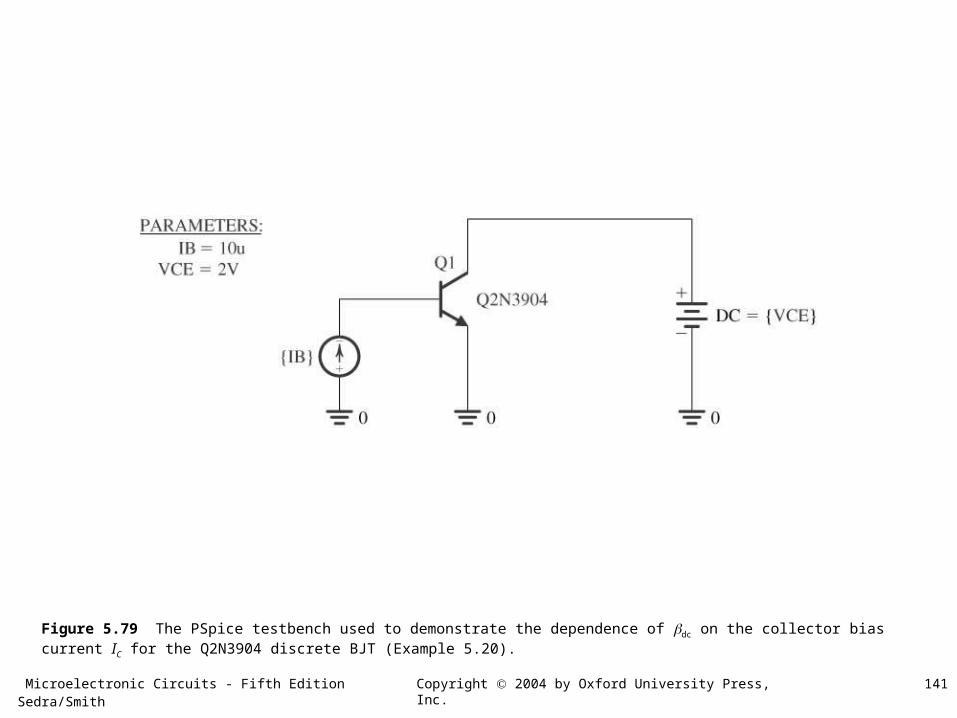
Figure 5.79 The PSpice testbench used to demonstrate the dependence of dc on the collector bias current IC for the Q2N3904 discrete BJT (Example 5.20).

Microelectronic Circuits - Fifth Edition Sedra/Smith 142Copyright 2004 by Oxford University Press, Inc.
Figure 5.80 Dependence of dc on IC (at VCE 5 2 V) in the Q2N3904 discrete BJT (Example 5.20).

Microelectronic Circuits - Fifth Edition Sedra/Smith 143Copyright 2004 by Oxford University Press, Inc.
Figure 5.81 Capture schematic of the CE amplifier in Example 5.21.
Microelectronic Circuits - Fifth Edition Sedra/Smith 144Copyright 2004 by Oxford University Press, Inc.
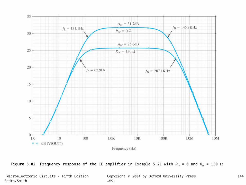
Figure 5.82 Frequency response of the CE amplifier in Example 5.21 with Rce = 0 and Rce = 130 .
Microelectronic Circuits - Fifth Edition Sedra/Smith 145Copyright 2004 by Oxford University Press, Inc.
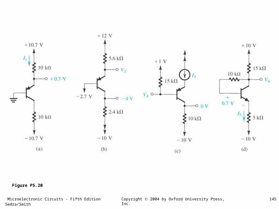
Figure P5.20

Microelectronic Circuits - Fifth Edition Sedra/Smith 146Copyright 2004 by Oxford University Press, Inc.
Figure P5.21
Microelectronic Circuits - Fifth Edition Sedra/Smith 147Copyright 2004 by Oxford University Press, Inc.
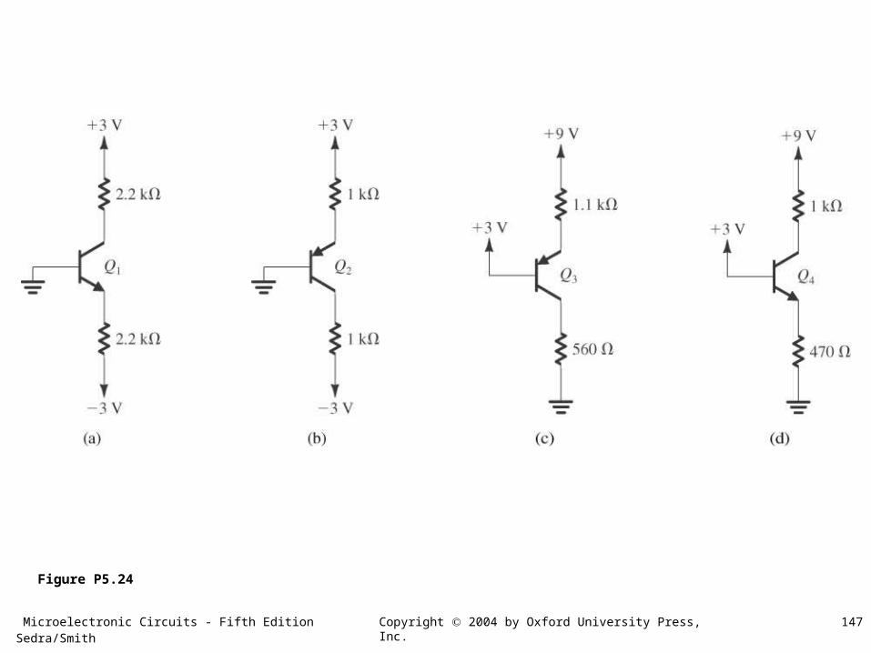
Figure P5.24
Microelectronic Circuits - Fifth Edition Sedra/Smith 148Copyright 2004 by Oxford University Press, Inc.
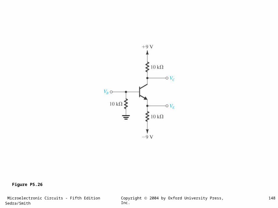
Figure P5.26
Microelectronic Circuits - Fifth Edition Sedra/Smith 149Copyright 2004 by Oxford University Press, Inc.
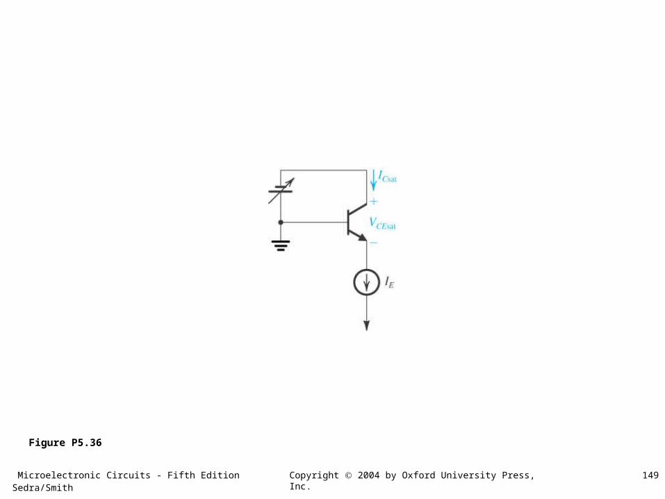
Figure P5.36
Microelectronic Circuits - Fifth Edition Sedra/Smith 150Copyright 2004 by Oxford University Press, Inc.
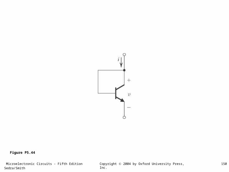
Figure P5.44
Microelectronic Circuits - Fifth Edition Sedra/Smith 151Copyright 2004 by Oxford University Press, Inc.
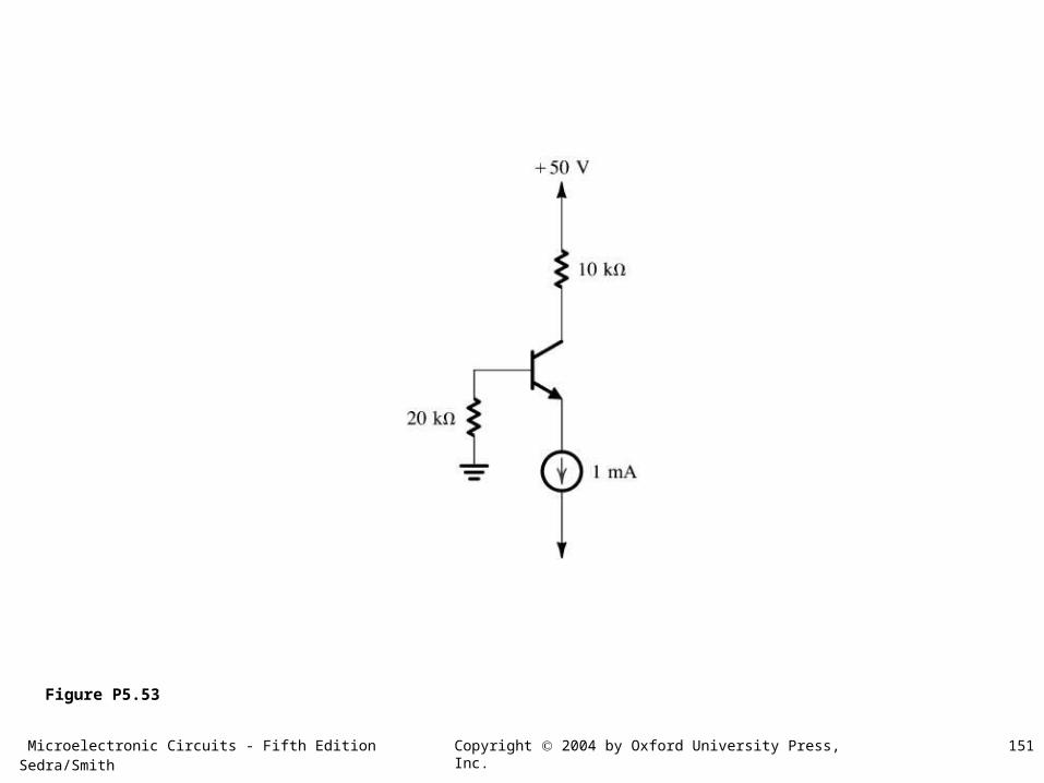
Figure P5.53
Microelectronic Circuits - Fifth Edition Sedra/Smith 152Copyright 2004 by Oxford University Press, Inc.
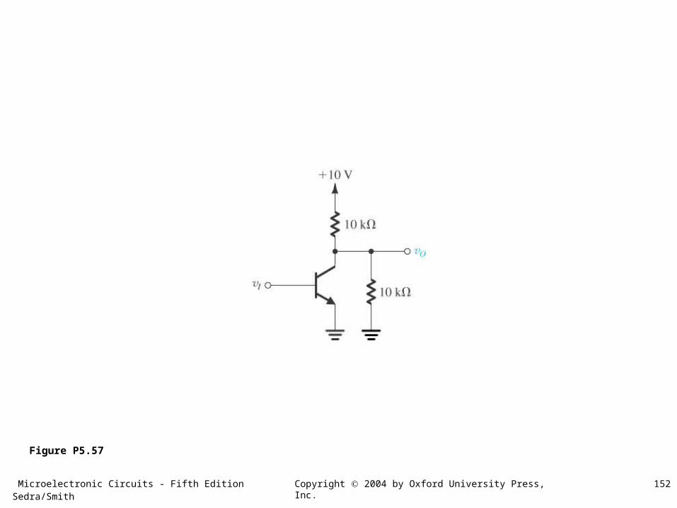
Figure P5.57

Microelectronic Circuits - Fifth Edition Sedra/Smith 153Copyright 2004 by Oxford University Press, Inc.
Figure P5.58
Microelectronic Circuits - Fifth Edition Sedra/Smith 154Copyright 2004 by Oxford University Press, Inc.
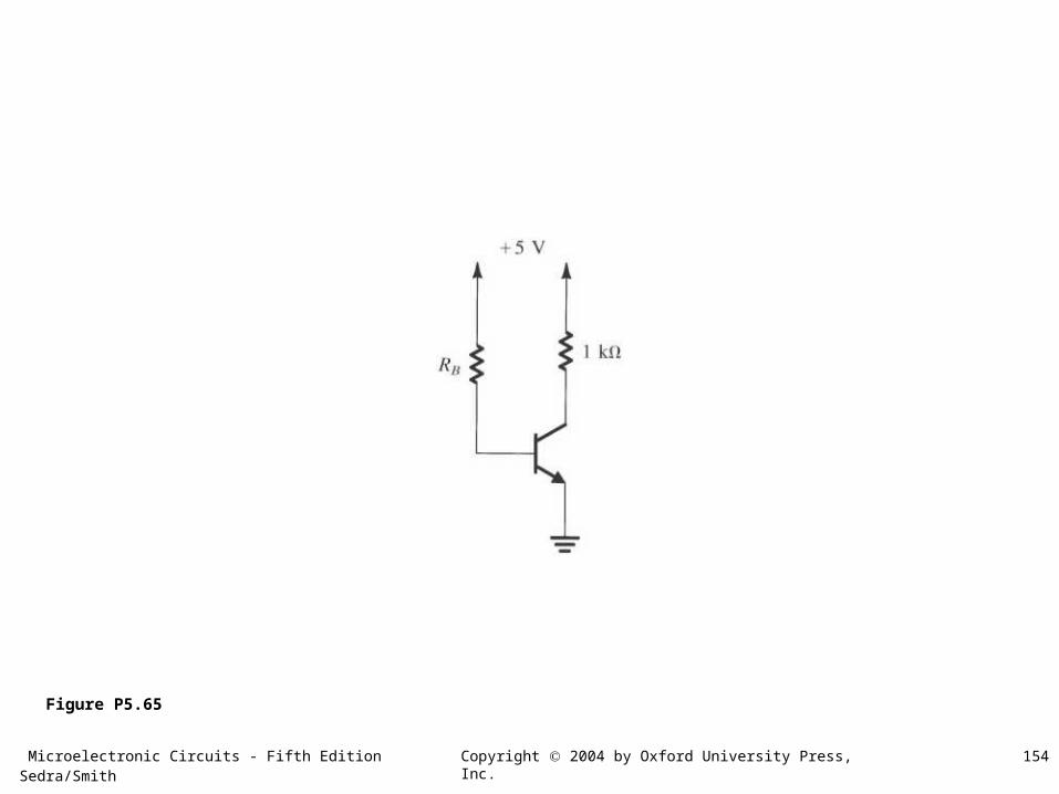
Figure P5.65
Microelectronic Circuits - Fifth Edition Sedra/Smith 155Copyright 2004 by Oxford University Press, Inc.
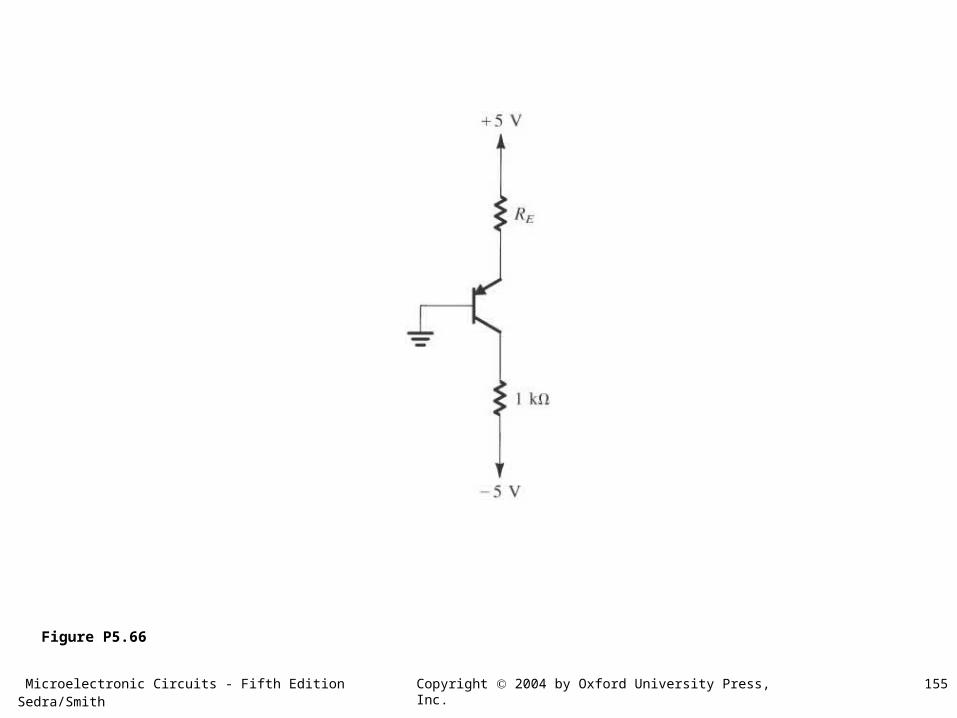
Figure P5.66

Microelectronic Circuits - Fifth Edition Sedra/Smith 156Copyright 2004 by Oxford University Press, Inc.
Figure P5.67

Microelectronic Circuits - Fifth Edition Sedra/Smith 157Copyright 2004 by Oxford University Press, Inc.
Figure P5.68
Microelectronic Circuits - Fifth Edition Sedra/Smith 158Copyright 2004 by Oxford University Press, Inc.
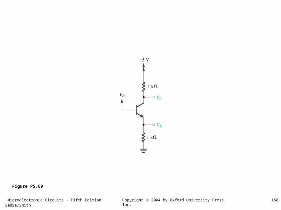
Figure P5.69
Microelectronic Circuits - Fifth Edition Sedra/Smith 159Copyright 2004 by Oxford University Press, Inc.
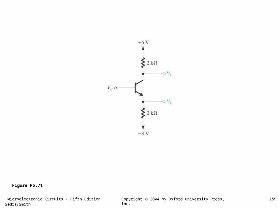
Figure P5.71

Microelectronic Circuits - Fifth Edition Sedra/Smith 160Copyright 2004 by Oxford University Press, Inc.
Figure P5.72

Microelectronic Circuits - Fifth Edition Sedra/Smith 161Copyright 2004 by Oxford University Press, Inc.
Figure P5.74
Microelectronic Circuits - Fifth Edition Sedra/Smith 162Copyright 2004 by Oxford University Press, Inc.
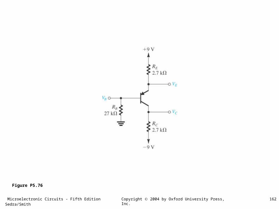
Figure P5.76
Microelectronic Circuits - Fifth Edition Sedra/Smith 163Copyright 2004 by Oxford University Press, Inc.
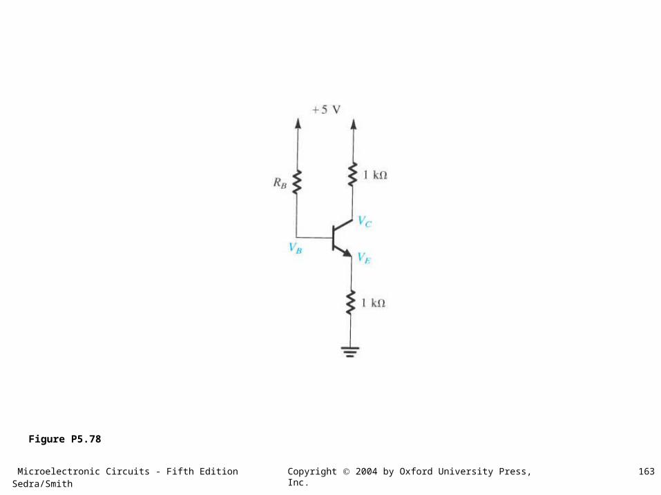
Figure P5.78
Microelectronic Circuits - Fifth Edition Sedra/Smith 164Copyright 2004 by Oxford University Press, Inc.
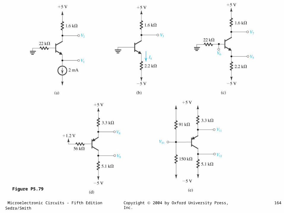
Figure P5.79

Microelectronic Circuits - Fifth Edition Sedra/Smith 165Copyright 2004 by Oxford University Press, Inc.
Figure P5.81

Microelectronic Circuits - Fifth Edition Sedra/Smith 166Copyright 2004 by Oxford University Press, Inc.
Figure P5.82

Microelectronic Circuits - Fifth Edition Sedra/Smith 167Copyright 2004 by Oxford University Press, Inc.
Figure P5.83
Microelectronic Circuits - Fifth Edition Sedra/Smith 168Copyright 2004 by Oxford University Press, Inc.
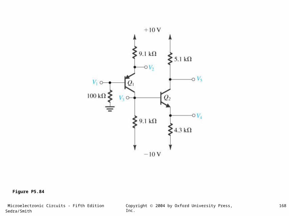
Figure P5.84
Microelectronic Circuits - Fifth Edition Sedra/Smith 169Copyright 2004 by Oxford University Press, Inc.
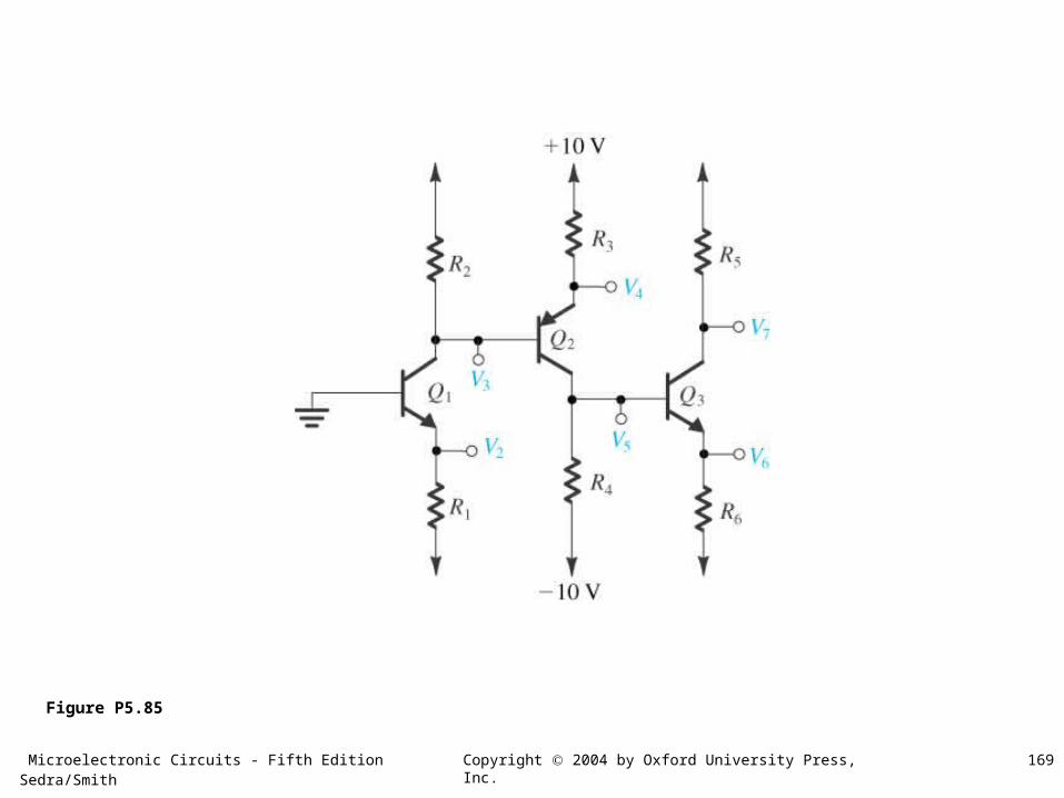
Figure P5.85

Microelectronic Circuits - Fifth Edition Sedra/Smith 170Copyright 2004 by Oxford University Press, Inc.
Figure P5.86

Microelectronic Circuits - Fifth Edition Sedra/Smith 171Copyright 2004 by Oxford University Press, Inc.
Figure P5.87

Microelectronic Circuits - Fifth Edition Sedra/Smith 172Copyright 2004 by Oxford University Press, Inc.
Figure P5.96

Microelectronic Circuits - Fifth Edition Sedra/Smith 173Copyright 2004 by Oxford University Press, Inc.
Figure P5.97

Microelectronic Circuits - Fifth Edition Sedra/Smith 174Copyright 2004 by Oxford University Press, Inc.
Figure P5.98

Microelectronic Circuits - Fifth Edition Sedra/Smith 175Copyright 2004 by Oxford University Press, Inc.
Figure P5.99
Microelectronic Circuits - Fifth Edition Sedra/Smith 176Copyright 2004 by Oxford University Press, Inc.
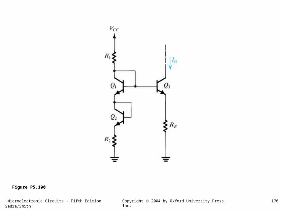
Figure P5.100

Microelectronic Circuits - Fifth Edition Sedra/Smith 177Copyright 2004 by Oxford University Press, Inc.
Figure P5.101
Microelectronic Circuits - Fifth Edition Sedra/Smith 178Copyright 2004 by Oxford University Press, Inc.
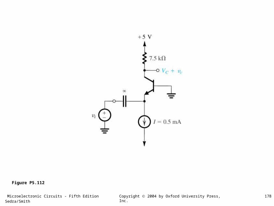
Figure P5.112
Microelectronic Circuits - Fifth Edition Sedra/Smith 179Copyright 2004 by Oxford University Press, Inc.
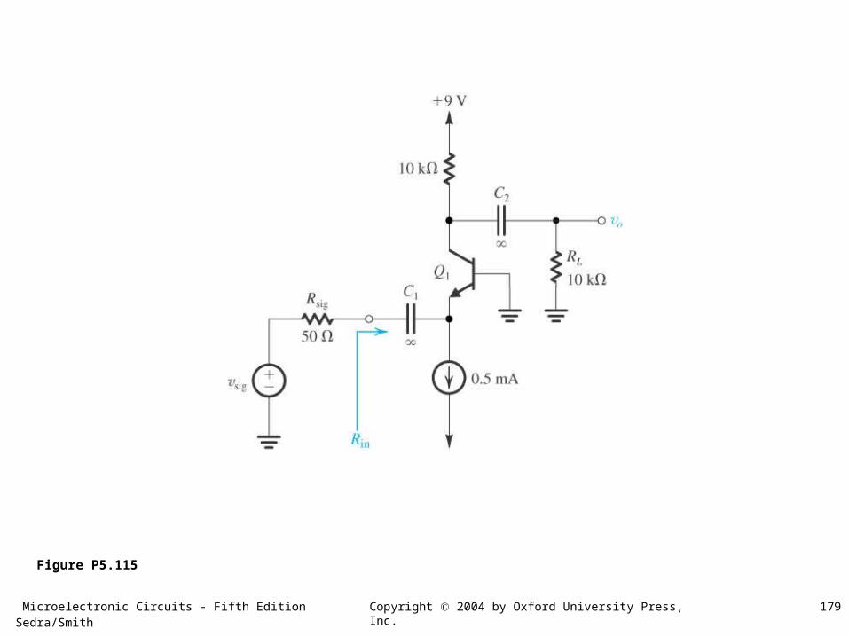
Figure P5.115
Microelectronic Circuits - Fifth Edition Sedra/Smith 180Copyright 2004 by Oxford University Press, Inc.
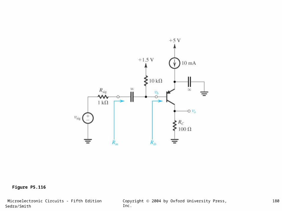
Figure P5.116
Microelectronic Circuits - Fifth Edition Sedra/Smith 181Copyright 2004 by Oxford University Press, Inc.
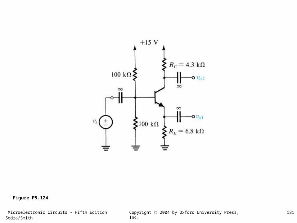
Figure P5.124

Microelectronic Circuits - Fifth Edition Sedra/Smith 182Copyright 2004 by Oxford University Press, Inc.
Figure P5.126
Microelectronic Circuits - Fifth Edition Sedra/Smith 183Copyright 2004 by Oxford University Press, Inc.
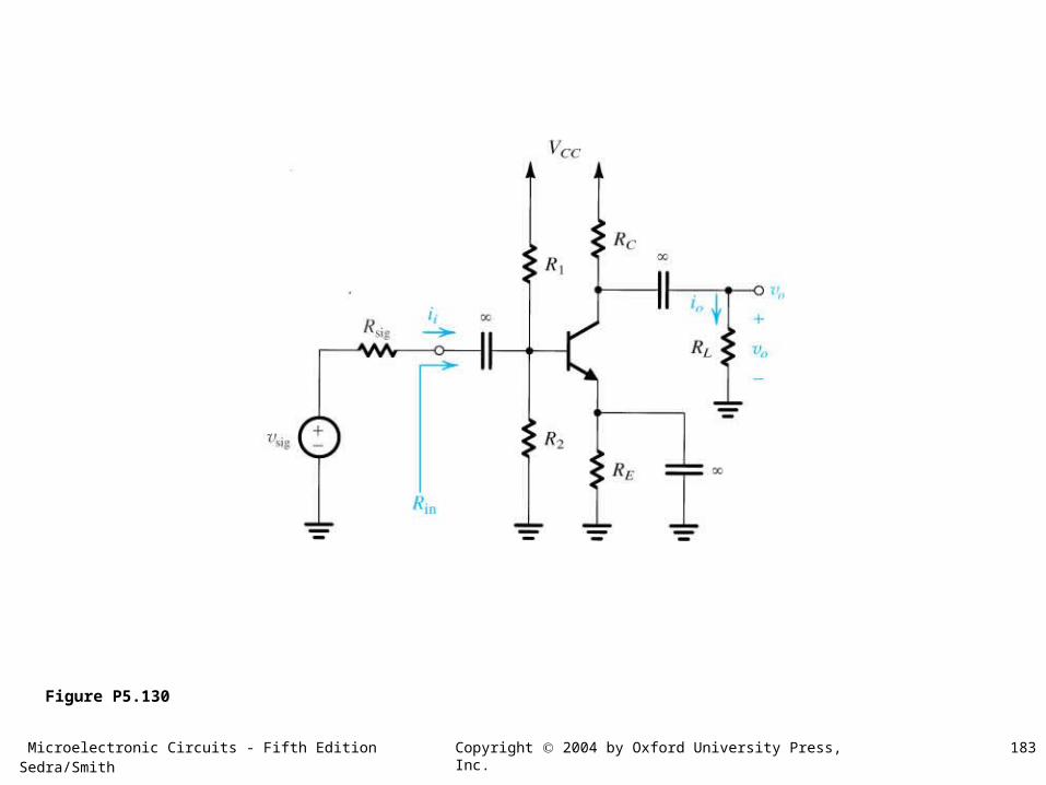
Figure P5.130
Microelectronic Circuits - Fifth Edition Sedra/Smith 184Copyright 2004 by Oxford University Press, Inc.
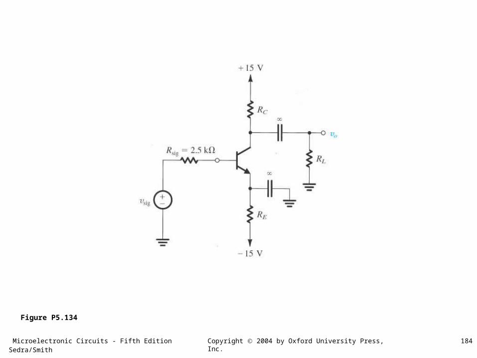
Figure P5.134
Microelectronic Circuits - Fifth Edition Sedra/Smith 185Copyright 2004 by Oxford University Press, Inc.
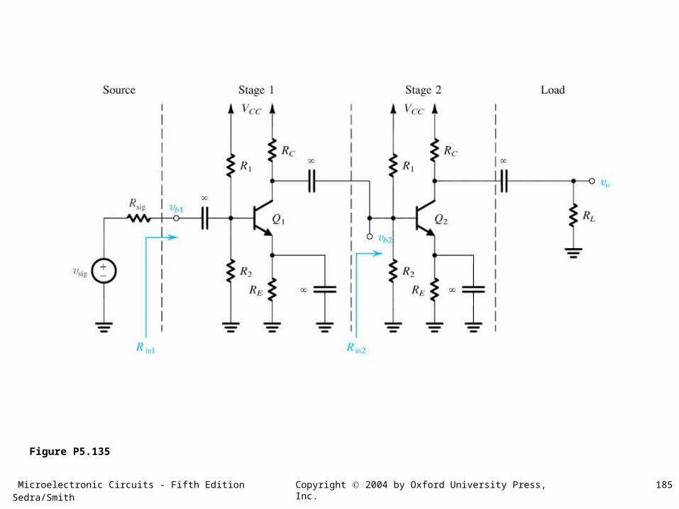
Figure P5.135
Microelectronic Circuits - Fifth Edition Sedra/Smith 186Copyright 2004 by Oxford University Press, Inc.
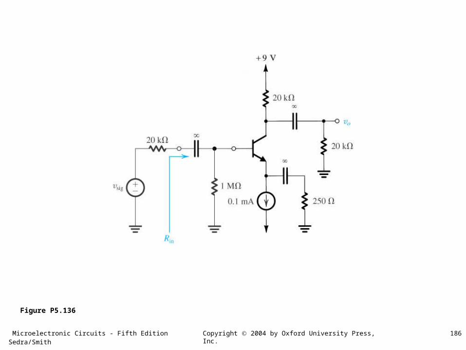
Figure P5.136

Microelectronic Circuits - Fifth Edition Sedra/Smith 187Copyright 2004 by Oxford University Press, Inc.
Figure P5.137

Microelectronic Circuits - Fifth Edition Sedra/Smith 188Copyright 2004 by Oxford University Press, Inc.
Figure P5.141

Microelectronic Circuits - Fifth Edition Sedra/Smith 189Copyright 2004 by Oxford University Press, Inc.
Figure P5.143
Microelectronic Circuits - Fifth Edition Sedra/Smith 190Copyright 2004 by Oxford University Press, Inc.
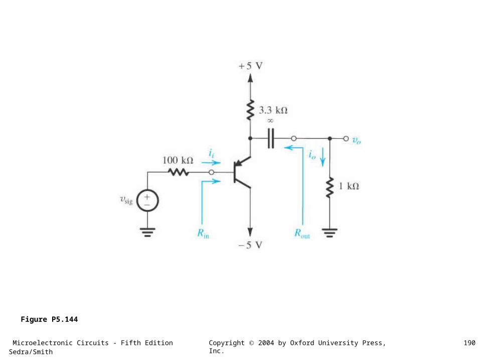
Figure P5.144

Microelectronic Circuits - Fifth Edition Sedra/Smith 191Copyright 2004 by Oxford University Press, Inc.
Figure P5.147

Microelectronic Circuits - Fifth Edition Sedra/Smith 192Copyright 2004 by Oxford University Press, Inc.
Figure P5.148

Microelectronic Circuits - Fifth Edition Sedra/Smith 193Copyright 2004 by Oxford University Press, Inc.
Figure P5.159

Microelectronic Circuits - Fifth Edition Sedra/Smith 194Copyright 2004 by Oxford University Press, Inc.
Figure P5.161
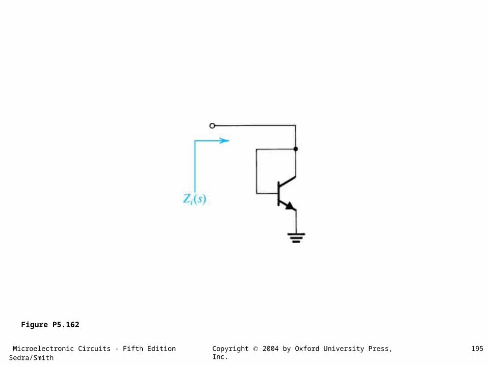
Microelectronic Circuits - Fifth Edition Sedra/Smith 195Copyright 2004 by Oxford University Press, Inc.
Figure P5.162
Microelectronic Circuits - Fifth Edition Sedra/Smith 196Copyright 2004 by Oxford University Press, Inc.
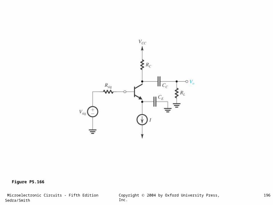
Figure P5.166
Microelectronic Circuits - Fifth Edition Sedra/Smith 197Copyright 2004 by Oxford University Press, Inc.
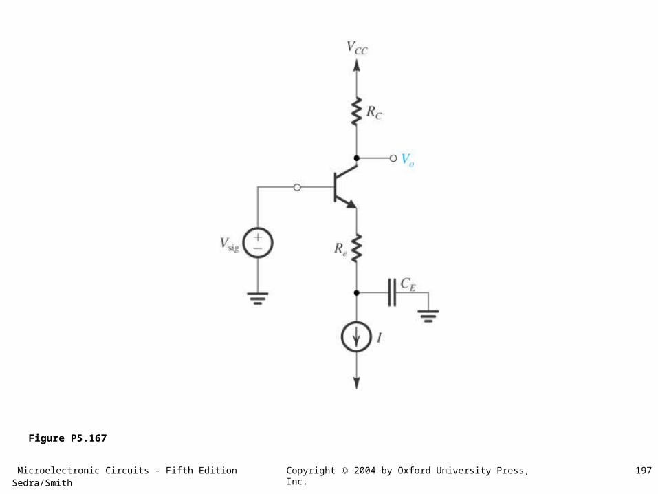
Figure P5.167

Microelectronic Circuits - Fifth Edition Sedra/Smith 198Copyright 2004 by Oxford University Press, Inc.
Figure P5.171


![Chapter 4 Introduction to Bipolar Junction Transistors (BJTs)bu.edu.eg/portal/uploads/Engineering, Shoubra/Electrical Engineering... · Figure 4.3 Forward-reverse bias of a BJT. [5]](https://static.fdocuments.in/doc/165x107/5ebfec4b97389926ad05ea31/chapter-4-introduction-to-bipolar-junction-transistors-bjtsbueduegportaluploadsengineering.jpg)