Memory Subsystems, SRAM,DRAM, Memory Compiler,Clock, Latency,Flip Flops, Latches
Upload
yudha-purnamaCategory
view
225download
0
8/8/2019 06a Latches, Flip Flops
http://slidepdf.com/reader/full/06a-latches-flip-flops 1/35
IKI1020106a-Latches & Flip-flops
Bobby Nazief
Semester-I 2005 - 2006
The materials on these slides are adopted from:
CS231·s Lecture Notes at UIUC, which is derived from Howard Huang·s work and developed by Jeff Carlyle;
Prof. Daniel Gajski·s transparency for Principles of Digital Design.

8/8/2019 06a Latches, Flip Flops
http://slidepdf.com/reader/full/06a-latches-flip-flops 2/35
2
Road Map
Boolean AlgebraLogic Gates &
Flip-flops
Register-TransferDesign
Finite-StateMachines
Binary Systems& Data Represent.
Generalized FSM
Sequential Design
Techniques
Logic Design
Techniques
CombinatorialComponents
StorageComponents
ProcessorComponents
2
3
3
4
5
6
7
6
8 8
9

8/8/2019 06a Latches, Flip Flops
http://slidepdf.com/reader/full/06a-latches-flip-flops 3/35
3
Combinational circuits
So far we·ve just worked with combinational circuits , where applying the same inputs always produces the same outputs.
This corresponds to a mathematical function, where every input has a single, unique output.
In programming terminology, combinational circuits are similar to ´functional programsµ that do not contain variables and assignments.
Combinational circuit Inputs Outputs

8/8/2019 06a Latches, Flip Flops
http://slidepdf.com/reader/full/06a-latches-flip-flops 4/35
Sequential circuits
In contrast, the outputs of a sequential circuit depend on not only the inputs, but also the state , or the current contents of some memory .
This makes things more difficult to understand, since the same inputs can yield different outputs, depending on what·s stored in memory.
The memory contents can also change as the circuit runs.
We·ll need some new techniques for analyzing and designing sequential circuits.
Combinational circuit
Inputs
Memory
Outputs
8/8/2019 06a Latches, Flip Flops
http://slidepdf.com/reader/full/06a-latches-flip-flops 5/35
5
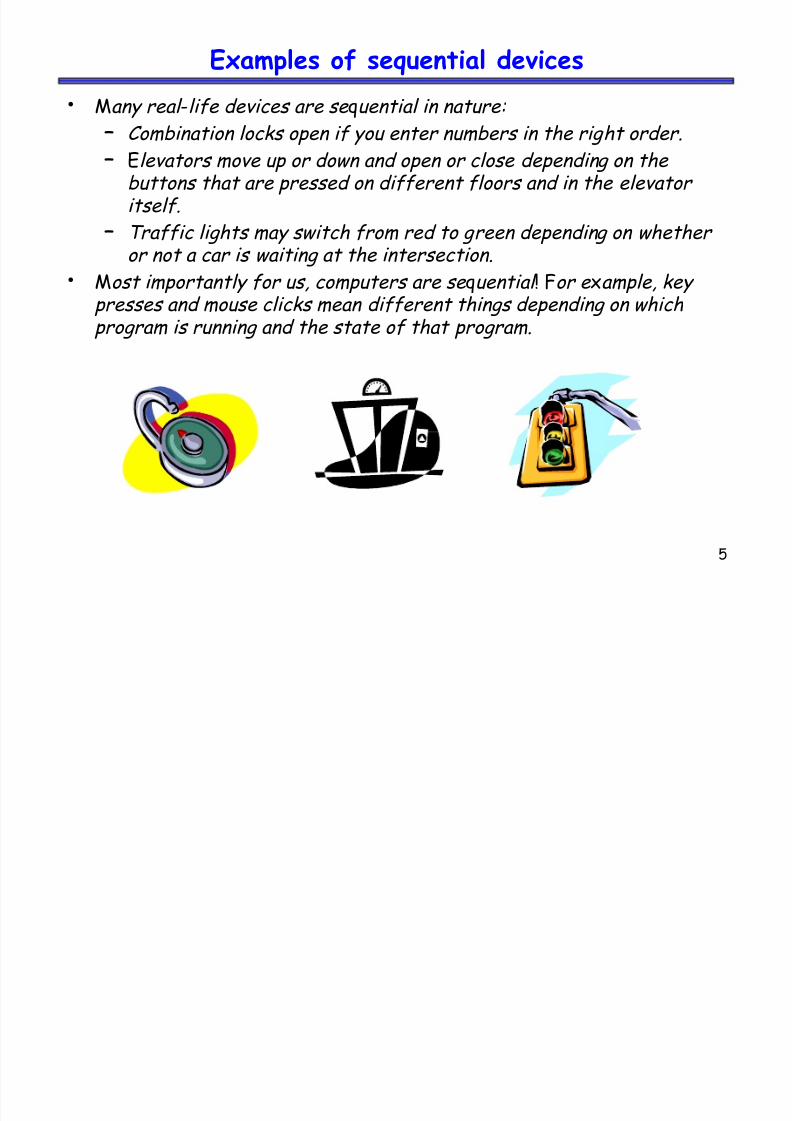
Examples of sequential devices
Many real-life devices are sequential in nature:
² Combination locks open if you enter numbers in the right order.² Elevators move up or down and open or close depending on the
buttons that are pressed on different floors and in the elevator itself.
² Traffic lights may switch from red to green depending on whether or not a car is waiting at the intersection.
Most importantly for us, computers are sequential! For example, key presses and mouse clicks mean different things depending on which program is running and the state of that program.

8/8/2019 06a Latches, Flip Flops
http://slidepdf.com/reader/full/06a-latches-flip-flops 6/35
6
Asynchronous vs. synchronous sequential circuits
Asynchronous sequential circuits change their states and output values
whenever a change in input values occurs Synchronous sequential circuits change their states and output values at fixed points of time, which are specified by the rising or falling edge of a free-running clock signal
A clock is a special device that whose output continuously alternates between 0 and 1.
² The time it takes the clock to change from 1 to 0 and back to 1 is
called the clock period , or clock cycle time .² The clock frequency is the inverse of the clock period. The unit of measurement for frequency is the hertz.
clock period

8/8/2019 06a Latches, Flip Flops
http://slidepdf.com/reader/full/06a-latches-flip-flops 7/35
More about clocks
Clocks are used extensively in computer architecture.
Nearly all processors run with an internal clock.² Modern chips run at frequencies up to 3.2 GHz.
² This works out to a cycle time as little as 0.31 ns!
Memory modules are often rated by their clock speeds too³examples include ´PC1 33µ and ´DDR400µ memory.

8/8/2019 06a Latches, Flip Flops
http://slidepdf.com/reader/full/06a-latches-flip-flops 8/35
8
What exactly is memory?
A memory should have at least three properties.
1. It should be able to hold a value.2. You should be able to read the value that was saved.
3. You should be able to change the value that·s saved.
We·ll start with the simplest case, a one-bit memory.
1. It should be able to hold a single bit, 0 or 1.2. You should be able to read the bit that was saved.
3. You should be able to change the value. Since there·s only a single bit, there are only two choices:
² Set the bit to 1
² Reset , or clear , the bit to 0.
8/8/2019 06a Latches, Flip Flops
http://slidepdf.com/reader/full/06a-latches-flip-flops 9/35
9
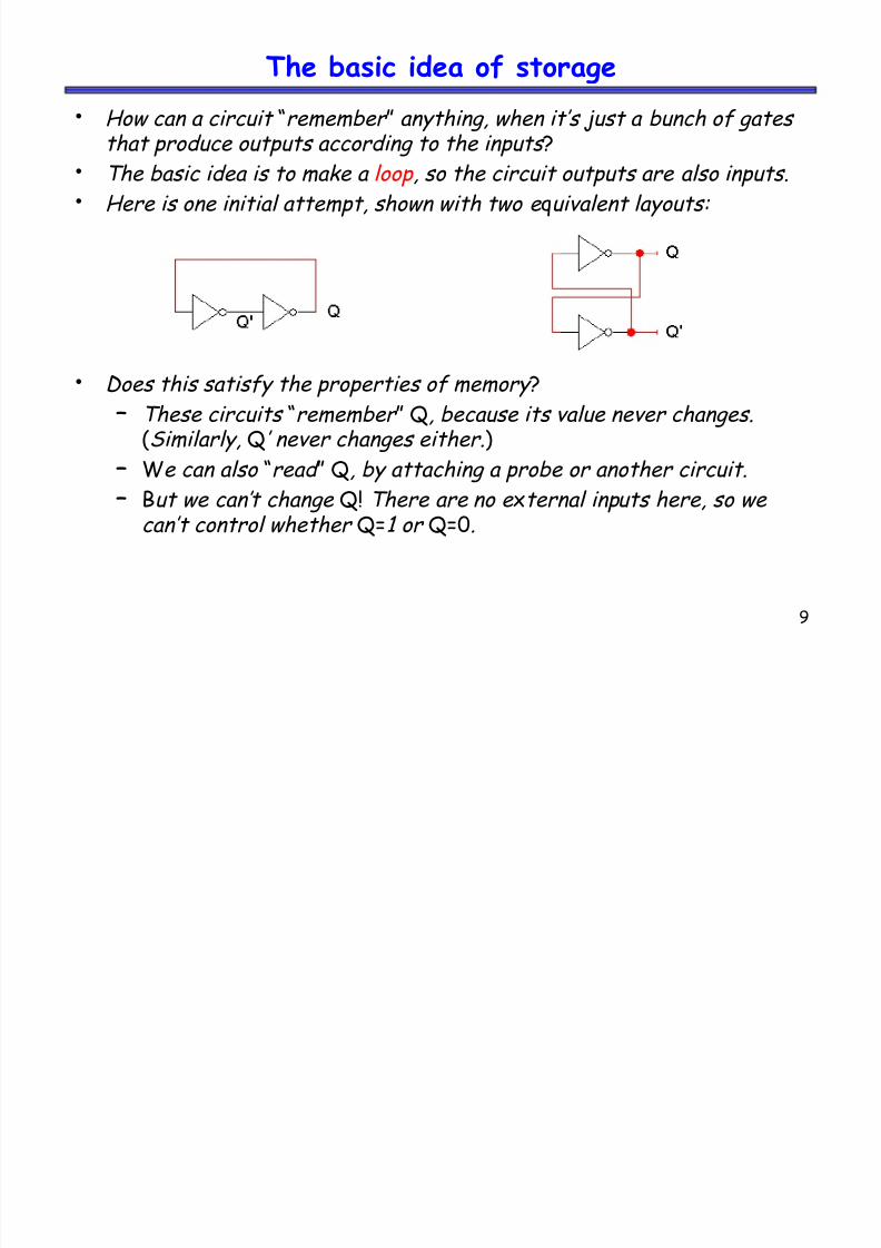
The basic idea of storage
How can a circuit ´rememberµ anything, when it·s just a bunch of gates
that produce outputs according to the inputs? The basic idea is to make a loop , so the circuit outputs are also inputs.
Here is one initial attempt, shown with two equivalent layouts:
Does this satisfy the properties of memory?
² These circuits ´rememberµ Q, because its value never changes.(Similarly, Q· never changes either.)
² We can also ´readµ Q, by attaching a probe or another circuit.² But we can·t change Q! There are no external inputs here, so we
can·t control whether Q=1 or Q=0.

8/8/2019 06a Latches, Flip Flops
http://slidepdf.com/reader/full/06a-latches-flip-flops 10/35
10
SR latch
Let·s use NOR gates instead of inverters. The SR latch below has two
inputs S and R, which will let us control the outputs Q and Q·.
Here Q and Q· feed back into the circuit. They·re not only outputs,they·re also inputs!
To figure out how Q and Q· change, we have to look at not only the inputs S and R, but also the current values of Q and Q·:
Qnext
= (R + Q· current
)·
Q· next = (S + Qcurrent )·
Let·s see how different input values for S and R affect this thing.

8/8/2019 06a Latches, Flip Flops
http://slidepdf.com/reader/full/06a-latches-flip-flops 11/35
11
Storing a value: SR = 00
What if S = 0 and R = 0?
The equations on the right reduce to:
Qnext = (0 + Q· current )· = Qcurrent
Q· next = (0 + Qcurrent )· = Q· current
So when SR = 00, then Qnext = Qcurrent .Whatever value Q has, it keeps.
This is exactly what we need to store values in the latch.
Qnext = (R + Q· current )· Q· next = (S + Qcurrent )·

8/8/2019 06a Latches, Flip Flops
http://slidepdf.com/reader/full/06a-latches-flip-flops 12/35
1 2
Setting the latch: SR = 10
What if S = 1 and R = 0?
Since S = 1, Q· next is 0, regardless of Qcurrent :
Q· next = (1 + Qcurrent )· = 0
Then, this new value of Q· goes into the top NOR gate, along with R = 0.
Qnext = (0 + 0)· = 1
So when SR = 10, then Q· next = 0 and Qnext = 1.
This is how you set the latch to 1. The S input stands for ´set.µ
Notice that it can take up to two steps (two gate delays ) from the time S becomes 1 to the time Qnext becomes 1.
But once Qnext becomes 1, the outputs will stop changing. This is a stable state .
Qnext = (R + Q· current )· Q· next = (S + Qcurrent )·

8/8/2019 06a Latches, Flip Flops
http://slidepdf.com/reader/full/06a-latches-flip-flops 13/35

8/8/2019 06a Latches, Flip Flops
http://slidepdf.com/reader/full/06a-latches-flip-flops 14/35
14
Resetting the latch: SR = 01
What if S = 0 and R = 1?
Since R = 1, Qnext is 0, regardless of Qcurrent : Qnext = (1 + Q· current )· = 0
Then, this new value of Q goes into the bottom NOR gate, where S = 0.
Q· next = (0 + 0)· = 1
So when SR = 01, then Qnext = 0 and Q· next = 1.
This is how you reset , or clear , the latch to 0.The R input stands for ´reset.µ
Again, it can take two gate delays before a
change in R propagates to the output Q· next .
Qnext = (R + Q· current )· Q· next = (S + Qcurrent )·
8/8/2019 06a Latches, Flip Flops
http://slidepdf.com/reader/full/06a-latches-flip-flops 15/35
1 5
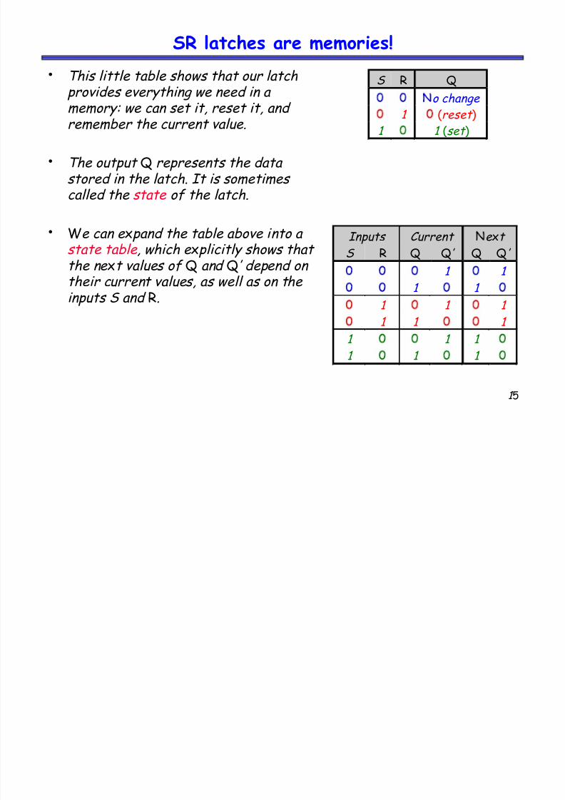
SR latches are memories!
This little table shows that our latch
provides everything we need in a memory: we can set it, reset it, and remember the current value.
The output Q represents the data stored in the latch. It is sometimes
called the state of the latch.
We can expand the table above into a state table , which explicitly shows that the next values of Q and Q· depend on their current values, as well as on the
inputs S and R.
S R Q
o change 1 (reset)
1 1 (set)
Inputs Current ext
S R Q Q· Q Q·
1 1
1 1
1 1 1
1 1 1
1 1 1
1 1 1

8/8/2019 06a Latches, Flip Flops
http://slidepdf.com/reader/full/06a-latches-flip-flops 16/35
1 6
SR latches are sequential!
Notice that for inputs SR = 00, the
next value of Q could be either 0 or 1,depending on the current value of Q.
So the same inputs can yield different outputs, depending on whether the latch was previously set or reset.
This is very different from the
combinational circuits that we·ve seen so far, where the same inputs always yield the same outputs.
Inputs Current Next
S R Q Q· Q Q·
0 0 0 1 0 1
0 0 1 0 1 0
0 1 0 1 0 1
0 1 1 0 0 1
1 0 0 1 1 0
1 0 1 0 1 0
S R Q
0 0 No change 0 1 0 (reset)
1 0 1 (set)

8/8/2019 06a Latches, Flip Flops
http://slidepdf.com/reader/full/06a-latches-flip-flops 17/35
17
What about SR = 11?
Both Qnext and Q· next will become 0.
This contradicts the assumption that Q and Q· are always complements.
Another problem is what happens if we then make S = 0 and R = 0 together.
Qnext = (0 + 0)· = 1
Q· next = (0 + 0)· = 1 But these new values go back into the NOR
gates, and in the next step we get:
Qnext = (0 + 1)· = 0
Q· next = (0 + 1)· = 0
The circuit enters an infinite loop, where Qand Q· cycle between 0 and 1 forever.
This is actually the worst case, but the moral is don·t ever set SR=11!
Qnext = (R + Q· current )· Q· next = (S + Qcurrent )·
0
0
0
0
0
0
1
1

8/8/2019 06a Latches, Flip Flops
http://slidepdf.com/reader/full/06a-latches-flip-flops 18/35
1 8
S·R· latch
There are several varieties of latches.
You can use NAND instead of NOR gates to get a S·R· latch .
This is just like an SR latch, but with inverted inputs, as you can see from the table.
You can derive this table by writing equations for the outputs in terms of the inputs and the current state, just as we did for the SR latch.
S· R·
1 1 No change
1 (reset)
1 1 (set)
Avoid!

8/8/2019 06a Latches, Flip Flops
http://slidepdf.com/reader/full/06a-latches-flip-flops 19/35

8/8/2019 06a Latches, Flip Flops
http://slidepdf.com/reader/full/06a-latches-flip-flops 20/35
20
Gated D latch
Finally, a D latch is based on an S·R· latch. The additional gates generate the S· and R· signals, based on inputs D (´dataµ) and C (´controlµ).
² When C = 0, S· and R· are both 1, so the state Q does not change.
² When C = 1, the latch output Q will equal the input D.
No more messing with one input for set and another input for reset!
Also, this latch has no ´badµ input combinations to avoid. Any of the four possible assignments to C and D are valid.
C D Q
0 No change
1 0 0
1 1 1

8/8/2019 06a Latches, Flip Flops
http://slidepdf.com/reader/full/06a-latches-flip-flops 21/35
21
Problems with latches
The circuit shows a 3-bit shift register using 3 D-latches.
Ideally, output of the D-latches should be 100,
010, 001 following 3 consecutive clocks.
Here, we have 111,000, 000.
Clock width may
be shorten, but exact width can not be set since set & reset delays are not the same!

8/8/2019 06a Latches, Flip Flops
http://slidepdf.com/reader/full/06a-latches-flip-flops 22/35
22
Summary
A sequential circuit has memory. It may respond differently to the same inputs, depending on its current state.
Memories can be created by making circuits with feedback.
² Latches are the simplest memory units, storing individual bits.
² It·s difficult to control the timing of latches in a larger circuit.
Next, we·ll improve upon latches with flip-flops , which change state only at well-defined times. We will then use flip-flops to build all of our
sequential circuits.

8/8/2019 06a Latches, Flip Flops
http://slidepdf.com/reader/full/06a-latches-flip-flops 23/35
23
Here is the internal structure of a D flip-flop .
² The flip-flop inputs are C and D, and the outputs are Q and Q·.² The D latch on the left is the master , while the SR latch on the right is called the slave .
Note the layout here.
² The flip-flop input D is connected directly to the master latch.
² The master latch output goes to the slave.
² The flip-flop outputs come directly from the slave latch.
Flip-flops

8/8/2019 06a Latches, Flip Flops
http://slidepdf.com/reader/full/06a-latches-flip-flops 24/35
24
The D flip-flop·s control input C enables either the D latch or the SRlatch, but not both .
When C = 0:
² The master latch is enabled, and it monitors the flip-flop input D.Whenever D changes, the master·s output changes too.
² The slave is disabled, so the D latch output has no effect on it.
Thus, the slave just maintains the flip-flop·s current state.
D flip-flops when C=0

8/8/2019 06a Latches, Flip Flops
http://slidepdf.com/reader/full/06a-latches-flip-flops 25/35
25
D flip-flops when C=1
As soon as C becomes 1, (i.e. on the rising edge of the clock)² The master is disabled. Its output will be the last D input value seen just before C became 1.
² Any subsequent changes to the D input while C = 1 have no effect on the master latch, which is now disabled.
² The slave latch is enabled. Its state changes to reflect the master·s
output, which again is the D input value from right when C became 1.

8/8/2019 06a Latches, Flip Flops
http://slidepdf.com/reader/full/06a-latches-flip-flops 26/35
26
Positive edge triggering
This is called a positive edge-triggered flip-flop.² The flip-flop output Q changes only after the positive edge of C.
² The change is based on the flip-flop input values that were present right at the positive edge of the clock signal.
The D flip-flop·s behavior is similar to that of a D latch except for the positive edge-triggered nature, which is not explicit in this table.
C D Q
x o change
1 (reset)
1 1 1 (set)

8/8/2019 06a Latches, Flip Flops
http://slidepdf.com/reader/full/06a-latches-flip-flops 27/35
27
Timing Diagram
C
D
QD
QSR

8/8/2019 06a Latches, Flip Flops
http://slidepdf.com/reader/full/06a-latches-flip-flops 28/35
28
Flip-flop variations
We can make different versions of flip-flops based on the D flip-flop, just like we made different latches based on the S·R· latch.
A JK flip-flop has inputs that act like S and R, but the inputs JK=11 are used to complement the flip-flop·s current state.
A T (toggle) flip-flop can only maintain or complement its current state.
T ne §
t
o change
1 o change
1 1 · current
J K ne §
t
o change
1 o change 1 1 (reset)
1 1 1 (set)
1 1 1 · current

8/8/2019 06a Latches, Flip Flops
http://slidepdf.com/reader/full/06a-latches-flip-flops 29/35
29
Characteristic tables
The tables that we·ve made so far are called characteristic tables .
² They show the next state Q(t+1)in terms of the current state Q(t)and the inputs.
² For simplicity, the control input C is not usually listed.
² Again, these tables don·t indicate the positive edge-triggered behavior of the flip-flops that we·ll be using.
Q(t+1) peration
eset
1 1 et
T Q(t+1) peration
Q(t) No change
1 Q·(t) Complement
J K Q(t+1) peration
Q(t) No change
1 eset
1 1 et
1 1 Q·(t) Complement

8/8/2019 06a Latches, Flip Flops
http://slidepdf.com/reader/full/06a-latches-flip-flops 30/35
30
Characteristic equations
We can also write characteristic equations , where the next state Q(t+1)is defined in terms of the current state Q(t) and inputs.
Q(t+1) peration
0 0 eset
1 1 et
T Q(t+1) peration
0 Q(t) No change
1 Q·(t) Complement
J K Q(t+1) peration
0 0 Q(t) No change
0 1 0 eset
1 0 1 et
1 1 Q·(t) Complement
Q(t+1) =
Q(t+1) = K·Q(t) + JQ·(t)
Q(t+1) = T·Q(t) + TQ·(t)= T Q(t)

8/8/2019 06a Latches, Flip Flops
http://slidepdf.com/reader/full/06a-latches-flip-flops 31/35
31
Flip flop timing diagrams
´Present stateµ and ´next stateµ are relative terms.
In the example JK flip-flop timing diagram on the left, you can see that at the first positive clock edge, J=1, K=1 and Q(1) = 1.
We can use this information to find the ´nextµ state, Q(2) = Q(1)·.
Q(2) appears right after the first positive clock edge, as shown on the right. It will not change again until after the second clock edge.
C
J
KQ
1 2 3 4
These values at clock cycle 1...
C
J
KQ
1 2 3 4
« determine the ´nextµ Q
8/8/2019 06a Latches, Flip Flops
http://slidepdf.com/reader/full/06a-latches-flip-flops 32/35
32
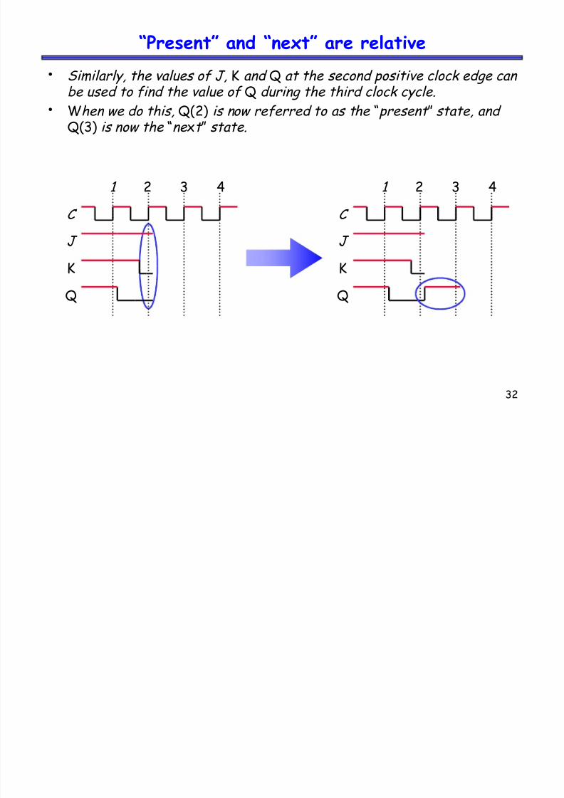
´Presentµ and ´nextµ are relative
Similarly, the values of J, K and Q at the second positive clock edge can be used to find the value of Q during the third clock cycle.
When we do this, Q(2) is now referred to as the ´presentµ state, and Q(3) is now the ´nextµ state.
C
J
K
Q
1 2 3 4
C
J
K
Q
1 2 3 4

8/8/2019 06a Latches, Flip Flops
http://slidepdf.com/reader/full/06a-latches-flip-flops 33/35
33
Positive edge triggered
One final point to repeat: the flip-flop outputs are affected only by the input values at the positive edge.
² In the diagram below, K changes rapidly between the second and third positive edges.
² But it·s only the input values at the third clock edge (K=1, and J=0and Q=1) that affect the next state, so here Q changes to 0.
This is a fairly simple timing model. In real life there are ´setup timesµ
and ´hold timesµ to worry about as well, to account for internal and external delays.
C
J K
Q
1 2 3 4

8/8/2019 06a Latches, Flip Flops
http://slidepdf.com/reader/full/06a-latches-flip-flops 34/35
34
State diagrams
To describe combinational circuits, we used Boolean expressions and truth tables. With sequential circuits, we can still use expression and tables, but we can also use another form called a state diagram .
The following state diagram represents a D flip-flop .
We draw one node for each state that the circuit can be in. Flip-flops have only two states: Q=0 and Q=1.
Arrows between nodes are labeled with input values and indicate how
the circuit changes states and what its output is (now shown, as the output and the state are the same).
D=1
D=1
D=0
Q=0 Q=1 D=0

8/8/2019 06a Latches, Flip Flops
http://slidepdf.com/reader/full/06a-latches-flip-flops 35/35
35
Summary
To use memory in a larger circuit, we need to:
² Keep the latches disabled until new values are ready to be stored.² Enable the latches just long enough for the update to occur.
A clock signal is used to synchronize circuits. The cycle time reflects how long combinational operations take.
Flip-flops further restrict the memory writing interval, to just the positive edge of the clock signal.
² This ensures that memory is updated only once per clock cycle.² There are several different kinds of flip-flops, but they all serve
the same basic purpose of storing bits.