Latches and Flip Flops - UCLAicslwebs.ee.ucla.edu/dejan/classwiki/images/6/61/Lec-10_Latches... ·...
26
EE M216A .:. Fall 2010 Lecture 10 Latches and Flip‐Flops Prof. Dejan Marković [email protected] Brief Introduction to Clocking / Latches & FFs Means to synchronize – By allowing events to happen at known timing boundaries, we can sequence these events Greatly eases building of FSMs – Clock strobe indicates the moment when states are stored No need to worry about variable delay through the CL – All signals are delayed until the clock edge (clock imposes the worst case delay) Dataflow FSM D. Markovic / Slide 2 register register register Comb Logic Comb Logic Lecture 10: Latches and Flip‐Flops | 2 EEM216A .:. Fall 2010
Transcript of Latches and Flip Flops - UCLAicslwebs.ee.ucla.edu/dejan/classwiki/images/6/61/Lec-10_Latches... ·...

1
EE M216A .:. Fall 2010Lecture 10
Latches and Flip‐Flops
Prof. Dejan Marković[email protected]
Brief Introduction to Clocking / Latches & FFs
Means to synchronize– By allowing events to happen at known timing boundaries, we
can sequence these eventsGreatly eases building of FSMsy g– Clock strobe indicates the moment when states are stored
No need to worry about variable delay through the CL– All signals are delayed until the clock edge
(clock imposes the worst case delay)
DataflowFSM
D. Markovic / Slide 2
register
register
register
CombLogic
CombLogic
Lecture 10: Latches and Flip‐Flops | 2EEM216A .:. Fall 2010

2
Positive Feedback: Bi‐Stability
State storage Vi1 Vo2Vo1 = Vi 2
Vo1 Vo1 =Vi2
Vo2 = Vi 1
Vi1
A
Vo2
V =Vi
D. Markovic / Slide 3EEM216A .:. Fall 2010 Lecture 10: Latches and Flip‐Flops | 3
C
B
Vi1 =Vo2
Vo1 =Vi2
Meta‐Stability
Gain should be larger than 1 in the transition region
AVo1 =Vi2
C
D. Markovic / Slide 4EEM216A .:. Fall 2010 Lecture 10: Latches and Flip‐Flops | 4
B
Vi1 =Vo2δV
3
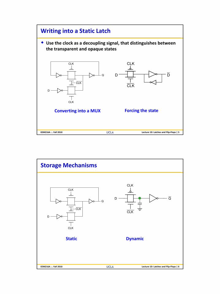
Writing into a Static Latch
Use the clock as a decoupling signal, that distinguishes between the transparent and opaque states
CLK
CLK
D
Q D
CLK
CLK
D
D. Markovic / Slide 5EEM216A .:. Fall 2010 Lecture 10: Latches and Flip‐Flops | 5
CLK
Converting into a MUX Forcing the state
Storage Mechanisms
CLKCLK
D
CLK
Q
CLK
CLK
D
Q
D. Markovic / Slide 6EEM216A .:. Fall 2010 Lecture 10: Latches and Flip‐Flops | 6
DynamicStatic
4
Pseudo‐Static Latch
CLKCLK
D
CLK
DD
CLK
Q
D. Markovic / Slide 7EEM216A .:. Fall 2010 Lecture 10: Latches and Flip‐Flops | 7
Dynamic Pseudo‐static
Latch versus Register
Latch: level‐sensitive– Clk low: hold mode– Clk high: transparent
Register: edge‐triggered– Stores on the Clk edge
(rising, falling, both)
D
Clk
Q D
Clk
Q
Clk Clk
D. Markovic / Slide 8EEM216A .:. Fall 2010 Lecture 10: Latches and Flip‐Flops | 8
D D
Q Q

5
Transmission Gate Latches
Simplest implementation Basic static latch
Complete implementation
Only 4 transistors Pull‐up/down keeper Feedback turned off
(a) (c)
ClkD Q Q
S
(b)
QSS
ClkD
ClkD
D. Markovic / Slide 9
yDynamic when S = 1Susceptible to noise
EEM216A .:. Fall 2010 Lecture 10: Latches and Flip‐Flops | 9
p/ pConflict at node Swhen writing new D
when writingNo conflictLarger Clk load
From: Oklobdzija et al., Wiley 2003
Cross‐Coupled NAND
This circuit is not used in datapaths anymore, but it is a basic building memory cell
Added clock
S
QR
Q
M
M2
M
M4Q
M6CLK M8 CLK
VDD
Q
D. Markovic / Slide 10EEM216A .:. Fall 2010 Lecture 10: Latches and Flip‐Flops | 10
R M1 M3
M5S M7 R

6
Principal Ways to Build a Register
Registers (flip‐flops) are built from latches– Master‐slave– Pulse‐triggered
D
Clk
Q D
Clk
Q
Clk
DD
Clk
Q
Clk
DL1 L2 L
D. Markovic / Slide 11EEM216A .:. Fall 2010 Lecture 10: Latches and Flip‐Flops | 11
Master‐Slave Latches
C
Pulse‐Triggered Latch
Characterizing Timing
Propagation delay (assumes that setup/hold are satisfied)
tD‐Q
D
Clk
Q D
Clk
Q
tClk‐Q tClk‐Q
D. Markovic / Slide 12EEM216A .:. Fall 2010 Lecture 10: Latches and Flip‐Flops | 12
Latch Register
Clk Q Clk Q
7
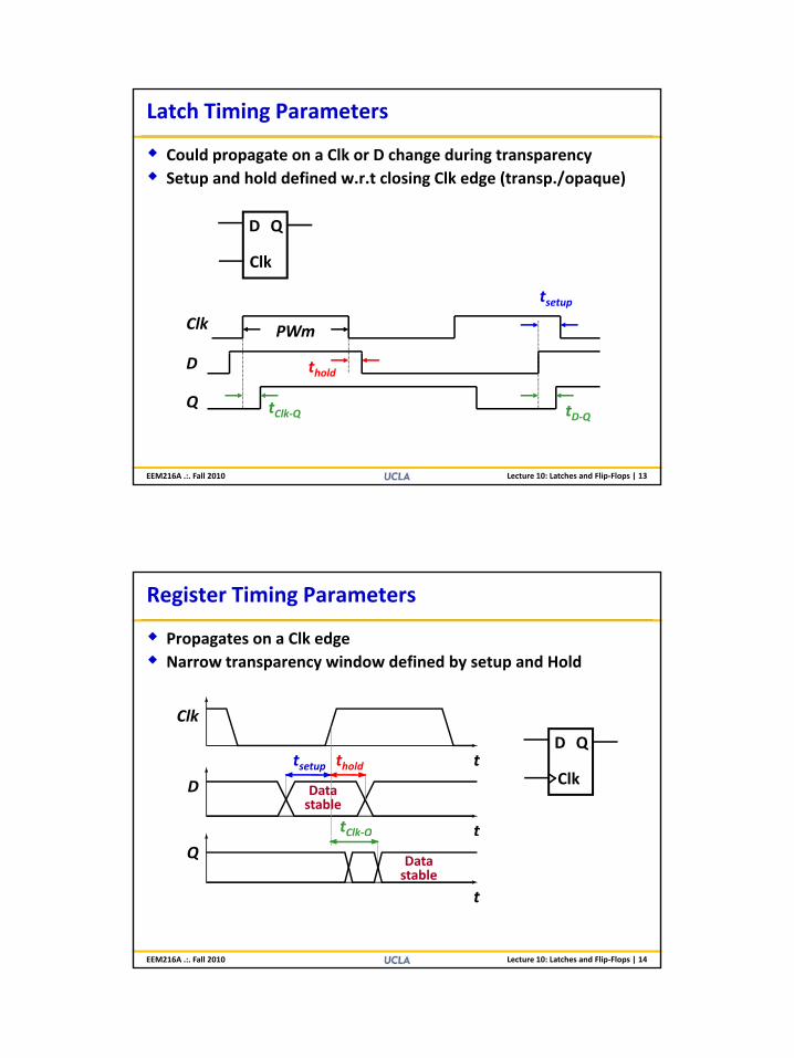
Latch Timing Parameters
Could propagate on a Clk or D change during transparencySetup and hold defined w.r.t closing Clk edge (transp./opaque)
D QD
Clk
Q
Clk PWm
tsetup
D. Markovic / Slide 13EEM216A .:. Fall 2010 Lecture 10: Latches and Flip‐Flops | 13
D
Q tClk‐Q
thold
tD‐Q
Register Timing Parameters
Propagates on a Clk edgeNarrow transparency window defined by setup and Hold
t
Clk
t
D Datastable
tsetup thold
tClk‐Q
D
Clk
Q
D. Markovic / Slide 14EEM216A .:. Fall 2010 Lecture 10: Latches and Flip‐Flops | 14
t
Q Datastable
8
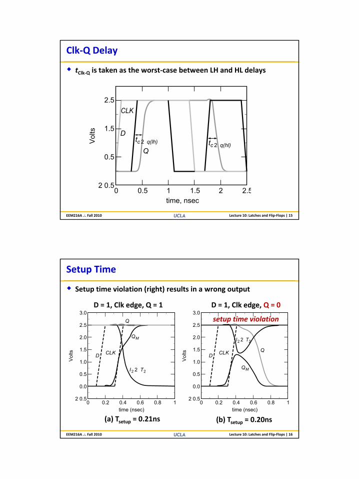
Clk‐Q Delay
tClk‐Q is taken as the worst‐case between LH and HL delays
2 5
D
Q
CLK
0.5
1.5
2.5
tc 2 q(lh)Vol
ts
tc 2 q(hl)
D. Markovic / Slide 15EEM216A .:. Fall 2010 Lecture 10: Latches and Flip‐Flops | 15
2 0.50.5 1 1.5 2 2.50
time, nsec
Setup Time
Setup time violation (right) results in a wrong output
3.0 3.0D = 1, Clk edge, Q = 1 D = 1, Clk edge, Q = 0
setup time violation
D
Q
QM
CLK
I2 2 T2
Vol
ts
0.5
1.0
1.5
2.0
2.5
DQ
QM
CLK
I2 2 T2
Vol
ts
0.5
1.0
1.5
2.0
2.5setup time violation
D. Markovic / Slide 16EEM216A .:. Fall 2010 Lecture 10: Latches and Flip‐Flops | 16
2 0.5
0.0
0.2 0.4time (nsec)
0.6 0.8 102 0.5
0.0
0.2 0.4time (nsec)
0.6 0.8 10
(a) Tsetup = 0.21ns (b) Tsetup = 0.20ns

9
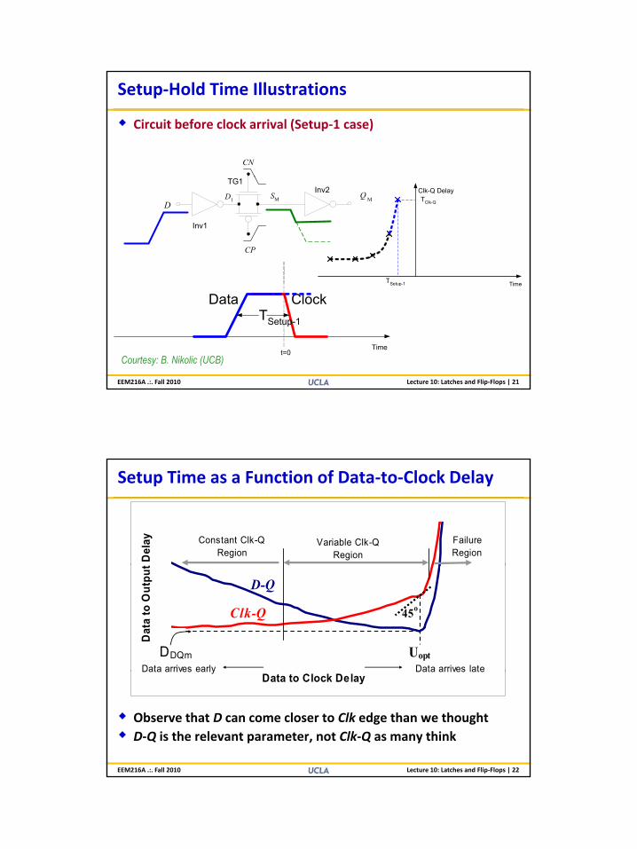
Setup‐Hold Time Illustrations
Circuit before clock arrival (Setup‐1 case)
CN
Clk-Q Delay
T
TClk-Q
Ti
DQM
CP
D1 SM
Inv1
Inv2TG1
D. Markovic / Slide 17EEM216A .:. Fall 2010 Lecture 10: Latches and Flip‐Flops | 17
TSetup-1 Time
Timet=0
ClockDataTSetup-1
Courtesy: B. Nikolic (UCB)
Setup‐Hold Time Illustrations
Circuit before clock arrival (Setup‐1 case)
CN
Clk-Q Delay
T
TClk-Q
DQM
CP
D1 SM
Inv1
Inv2TG1
D. Markovic / Slide 18EEM216A .:. Fall 2010 Lecture 10: Latches and Flip‐Flops | 18
TSetup-1 Time
Timet=0
ClockDataTSetup-1
Courtesy: B. Nikolic (UCB)

10
Setup‐Hold Time Illustrations
Circuit before clock arrival (Setup‐1 case)
CN
Clk-Q Delay
TS t 1
TClk-Q
Ti
DQM
CP
D1 SM
Inv1
Inv2TG1
D. Markovic / Slide 19EEM216A .:. Fall 2010 Lecture 10: Latches and Flip‐Flops | 19
TSetup-1 Time
Timet=0
ClockDataTSetup-1
Courtesy: B. Nikolic (UCB)
Setup‐Hold Time Illustrations
Circuit before clock arrival (Setup‐1 case)
CN
Clk-Q Delay
TS t 1
TClk-Q
Ti
DQM
CP
D1 SM
Inv1
Inv2TG1
D. Markovic / Slide 20EEM216A .:. Fall 2010 Lecture 10: Latches and Flip‐Flops | 20
TSetup-1 Time
Timet=0
ClockDataTSetup-1
Courtesy: B. Nikolic (UCB)
11
Setup‐Hold Time Illustrations
Circuit before clock arrival (Setup‐1 case)
CN
DQM
CP
D1 SM
Inv1
Inv2TG1
Clk-Q Delay
TSetup 1
TClk-Q
Time
D. Markovic / Slide 21EEM216A .:. Fall 2010 Lecture 10: Latches and Flip‐Flops | 21
Timet=0
ClockDataTSetup-1
Setup-1 Time
Courtesy: B. Nikolic (UCB)
Del
ay Constant Clk-Q Region
Failure Region
Variable Clk-Q Region
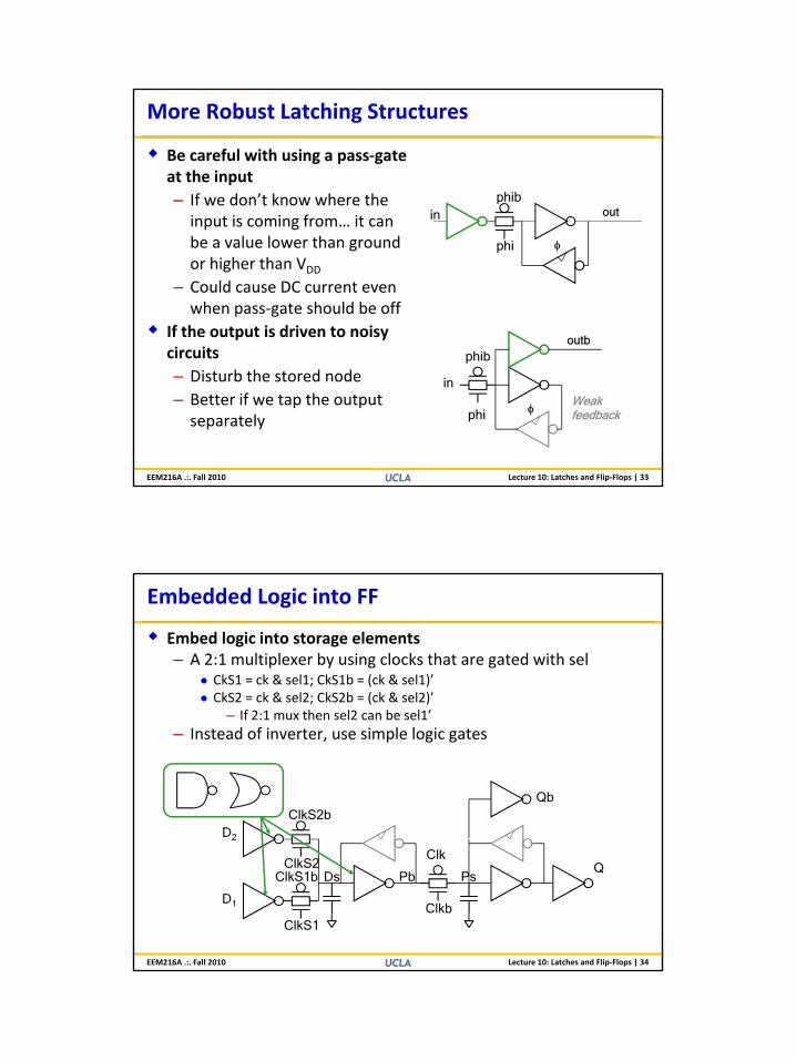
Setup Time as a Function of Data‐to‐Clock Delay
Dat
a to
Out
put
DDQmData arrives early Data arrives late
D-Q
Clk-Q
Uopt
45o
D. Markovic / Slide 22
Data to Clock DelayData arrives early Data arrives late
Lecture 10: Latches and Flip‐Flops | 22EEM216A .:. Fall 2010
Observe that D can come closer to Clk edge than we thoughtD‐Q is the relevant parameter, not Clk‐Q as many think

12
Data‐to‐Output Delay
Sum of setup time and Clk‐Q delay is the only true measure of system performanceTClk = TClk‐Q + TLogic + Tsetup+ Tskew
D Q
Clk
D Q
Clk
LogicN
D. Markovic / Slide 23
tLogictClk‐Q tSetup
TClk
tD‐Q = tClk‐Q + tSetup
Lecture 10: Latches and Flip‐Flops | 23EEM216A .:. Fall 2010
Setup‐Hold Time Illustrations
Hold‐1 case
CN
DQM
CP
D1 SM
Inv1
Inv2TG1
0
Clk-Q Delay
THold-1
TClk-Q
Time
D. Markovic / Slide 24EEM216A .:. Fall 2010 Lecture 10: Latches and Flip‐Flops | 24
Timet=0
DataClockTHold-1
Hold 1 Time
Courtesy: B. Nikolic (UCB)

13
Setup‐Hold Time Illustrations
Hold‐1 case
CN
Clk-Q Delay
THold-1
TClk-Q
Time
DQM
CP
D1 SM
Inv1
Inv2TG1
0
D. Markovic / Slide 25EEM216A .:. Fall 2010 Lecture 10: Latches and Flip‐Flops | 25
Hold 1 Time
Timet=0
DataClockTHold-1
Courtesy: B. Nikolic (UCB)
Setup‐Hold Time Illustrations
Hold‐1 case
CN
Clk-Q Delay
THold-1
TClk-Q
Time
DQM
CP
D1 SM
Inv1
Inv2TG1
0
D. Markovic / Slide 26EEM216A .:. Fall 2010 Lecture 10: Latches and Flip‐Flops | 26
Time
Timet=0
DataClockTHold-1
Courtesy: B. Nikolic (UCB)

14
Setup‐Hold Time Illustrations
Hold‐1 case
CN
Clk-Q Delay
THold-1
TClk-Q
Time
DQM
CP
D1 SM
Inv1
Inv2TG1
0
D. Markovic / Slide 27EEM216A .:. Fall 2010 Lecture 10: Latches and Flip‐Flops | 27
Hold 1 Time
Timet=0
ClockTHold-1
Data
Courtesy: B. Nikolic (UCB)
Setup‐Hold Time Illustrations
Hold‐1 case
CN
Clk-Q Delay
THold-1
TClk-Q
Time
DQM
CP
D1 SM
Inv1
Inv2TG1
0
D. Markovic / Slide 28EEM216A .:. Fall 2010 Lecture 10: Latches and Flip‐Flops | 28
Hold 1 Time
Timet=0
Clock
THold-1
Data⇒
Courtesy: B. Nikolic (UCB)

15
300
350
Clk‐Q Delay vs. Setup and Hold Times
100
150
200
250
300
Clk
-Out
put [
ps]
Setup Hold
Sampling Window
D. Markovic / Slide 29
0
50
100
-200 -150 -100 -50 0 50 100 150 200Data-Clk [ps]
Sampling Window
Lecture 10: Latches and Flip‐Flops | 29EEM216A .:. Fall 2010
1 52.0
s]
Impact of VDD on the Sampling Window
2.2
2.5
0.51.01.5
V
t Clk
-Q [n
s
D. Markovic / Slide 30
-500-300
-100100
300
1
1.3
1.6
1.9
D-Clk [ps]
VDD [V]
Lecture 10: Latches and Flip‐Flops | 30EEM216A .:. Fall 2010

16
Simple Storage Elements
Latch– All nodes are driven at all times– Sizing of feedback portion small
D t d bi d i t h ld d t
Clk
QbDClkb
Clk
● Do not need big devices to hold data
ClkbFlip‐flop (master‐slave)– M passes D to Pb
when Clk = 0– S passes Pb to Q
when Clk = 1 QD Pb
Clk Clkb
D. Markovic / Slide 31Lecture 10: Latches and Flip‐Flops | 31EEM216A .:. Fall 2010
– D does not pass to Pb when Clk = 1
– D arrives just before the L‐H Clk edge
Clk
Clkb
ClkClkb
Clk
Clkb
Clocked Inverter
Another common element for building storage elements is a clocked‐inverter– Not too different from an inverter + pass‐gate
Eliminates the extra contact spacing between NMOS and PMOS– Eliminates the extra contact spacing between NMOS and PMOS so it is quite compact
– But does not pull down/up with both N/P
in
φbφ
out
φb
D. Markovic / Slide 32
in
outφin
outin
out
φ
Lecture 10: Latches and Flip‐Flops | 32EEM216A .:. Fall 2010
17
More Robust Latching Structures
Be careful with using a pass‐gate at the input– If we don’t know where the
input is coming from it can inphib
outinput is coming from… it can be a value lower than ground or higher than VDD
– Could cause DC current even when pass‐gate should be off
If the output is driven to noisy circuits phib
outb
φphi
D. Markovic / Slide 33
circuits– Disturb the stored node– Better if we tap the output
separatelyWeakfeedbackφ
in
phi
phib
Lecture 10: Latches and Flip‐Flops | 33EEM216A .:. Fall 2010
Embedded Logic into FF
Embed logic into storage elements– A 2:1 multiplexer by using clocks that are gated with sel
● CkS1 = ck & sel1; CkS1b = (ck & sel1)’● CkS2 = ck & sel2; CkS2b = (ck & sel2)’
– If 2:1 mux then sel2 can be sel1’– Instead of inverter, use simple logic gates
D2
ClkS2bQb
D. Markovic / Slide 34
ClkS1
Pb
D1
ClkS2Ds
Clkb
QClk
Ps
2
ClkS1b
Lecture 10: Latches and Flip‐Flops | 34EEM216A .:. Fall 2010

18
Enabled Flip‐Flop (or Latch)
New data is accepted only when Enable is HOtherwise retain old data
0D Q
EnD Q
QD Q
Conceptually, a mux before the F/F. Can use a built‐in mux
Or we can use a “qualified” clock
D. Markovic / Slide 35
1D Q
Clk
D
QEn
Clk
Lecture 10: Latches and Flip‐Flops | 35EEM216A .:. Fall 2010
Synchronous Reset
Some flip‐flops or latches embed very useful functions to help its operationSynchronous reset assumes that the reset (output L) occurs with the clock transitionthe clock transition
PbD DsQ
Clk
Ps
Qb
D. Markovic / Slide 36
Clk
PbDs
Clkb
Psrstb
Lecture 10: Latches and Flip‐Flops | 36EEM216A .:. Fall 2010
19
Asynchronous Reset
The output is cleared to Low whenever a reset signal arrivesNeed to clear the held value (state)A Set/Reset can also be made using feedback NAND gates
PbD
Ds QbClk
Ps
Q
rstb
D. Markovic / Slide 37
Clk
D
Clkbrstb
Lecture 10: Latches and Flip‐Flops | 37EEM216A .:. Fall 2010
C2MOS Flip‐Flop: Insensitive to Clock Overlap
Uses clocked inverter
φbφb
in
out
φb
φin
out
φ
inout
φ
φb
in
φb
φ outφb
φDs
One nice feature of this F/F is that
D. Markovic / Slide 38
φ outφb One nice feature of this F/F is thatit is not sensitive to φ‐to‐φb skew
Lecture 10: Latches and Flip‐Flops | 38EEM216A .:. Fall 2010
No current
20
Charge Injection
A problem with dynamic nodes is that it is high‐impedance and therefore very sensitive to noiseClock/Data switching can easily introduce charge
Often known as clock feedthrough– Often known as clock feedthrough
in Dynamic out
φb
φ
Ccoup
Coutin
φb
φData held is Low
Input L‐H transition
D. Markovic / Slide 39
φ
outcoup
coupinout CC
CVV
+∆=∆
Not a big concern for this FF, but it can be for other designs
Lecture 10: Latches and Flip‐Flops | 39EEM216A .:. Fall 2010
Charge Sharing
Similar to injection, charge on floating nodes can share (depending on the gate voltage) degrading the value of the floating nodesExample:Example:
inDynamic out
φb
φ
Cout
CP
in
φb
φ
Input H-L transition causes CP and Cout to share
D. Markovic / Slide 40
outfinalPfinalafteroutGNDPDDbefore CVCVQCVCVQ +==+=Cout discharged L
CP charged H
outP
PDDfinal CC
CVV+
= Be careful because if Cout!>>Cp, VCP !< -VTP.
Note that C2MOS inverter is not designed like this… for this reason.
Lecture 10: Latches and Flip‐Flops | 40EEM216A .:. Fall 2010
21
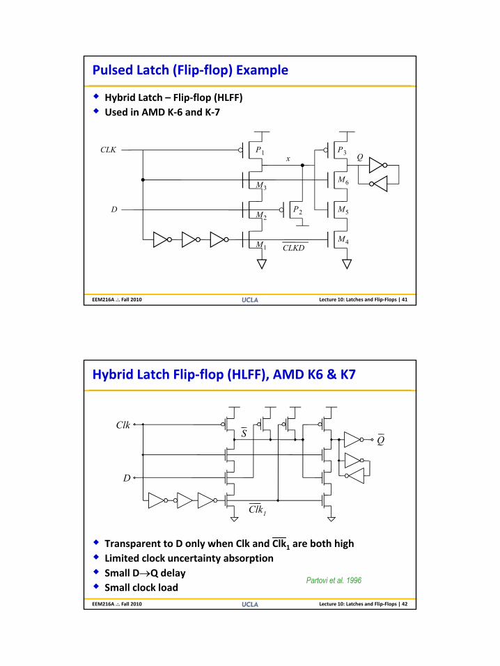
Pulsed Latch (Flip‐flop) Example
Hybrid Latch – Flip‐flop (HLFF)Used in AMD K‐6 and K‐7
P1
M3
M2D
CLK P3
M6
Qx
M5P2
D. Markovic / Slide 41EEM216A .:. Fall 2010 Lecture 10: Latches and Flip‐Flops | 41
M1M4
CLKD
Hybrid Latch Flip‐flop (HLFF), AMD K6 & K7
QClk
S
D
Q
Clk1
D. Markovic / Slide 42
Transparent to D only when Clk and Clk1 are both highLimited clock uncertainty absorptionSmall D→Q delaySmall clock load
EEM216A .:. Fall 2010 Lecture 10: Latches and Flip‐Flops | 42
Partovi et al. 1996

22
Vdd
Q
2nd Stage LatchPulseGenerator
HLFF Analysis
D
Clk
Q
D=1
D. Markovic / Slide 43
Clk
D=1
D=0
signal atnode X
D=0
From: Oklobdzija et al.Digital System Clocking, Wiley’03
Lecture 10: Latches and Flip‐Flops | 43EEM216A .:. Fall 2010
Clk
D
Q
Logic Representation of HLFF
Enable
2nd Stage Latch
PulseGenerator
D. Markovic / Slide 44
D=1
D=0signal atnode X
D=1
D=0Lecture 10: Latches and Flip‐Flops | 44EEM216A .:. Fall 2010
23
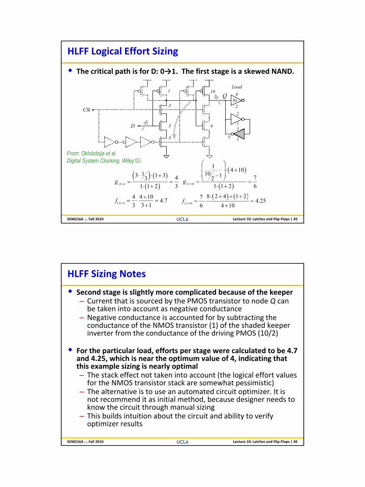
HLFF Logical Effort Sizing
The critical path is for D: 0→1. The first stage is a skewed NAND.
Q1 10 4
8x
Load
Clk
D
3
3
3
2
1
2
1
28x
4
From: Oklobdzija et al.Digital System Clocking, Wiley’03
D. Markovic / Slide 45EEM216A .:. Fall 2010 Lecture 10: Latches and Flip‐Flops | 45
( ) ( )( )1,0 1
13 1 3 431 1 2 3
g →
⋅ ⋅ += =
⋅ +
( )
( )2,1 0
1 4 1010 1 721 1 2 6
g →
⋅ + − = =
⋅ +
1,0 1
4 4 10 4.73 3 1
f →
+= ⋅ =
+( ) ( )
2,1 0
8 2 4 1 27 4.256 4 10
f →
⋅ + + += ⋅ =
+
Digital System Clocking, Wiley 03
HLFF Sizing Notes
Second stage is slightly more complicated because of the keeper– Current that is sourced by the PMOS transistor to node Q can
be taken into account as negative conductance– Negative conductance is accounted for by subtracting the
conductance of the NMOS transistor (1) of the shaded keeperconductance of the NMOS transistor (1) of the shaded keeper inverter from the conductance of the driving PMOS (10/2)
For the particular load, efforts per stage were calculated to be 4.7 and 4.25, which is near the optimum value of 4, indicating that this example sizing is nearly optimal– The stack effect not taken into account (the logical effort values
for the NMOS transistor stack are somewhat pessimistic)
D. Markovic / Slide 46
for the NMOS transistor stack are somewhat pessimistic)– The alternative is to use an automated circuit optimizer. It is
not recommend it as initial method, because designer needs to know the circuit through manual sizing
– This builds intuition about the circuit and ability to verify optimizer results
EEM216A .:. Fall 2010 Lecture 10: Latches and Flip‐Flops | 46
24
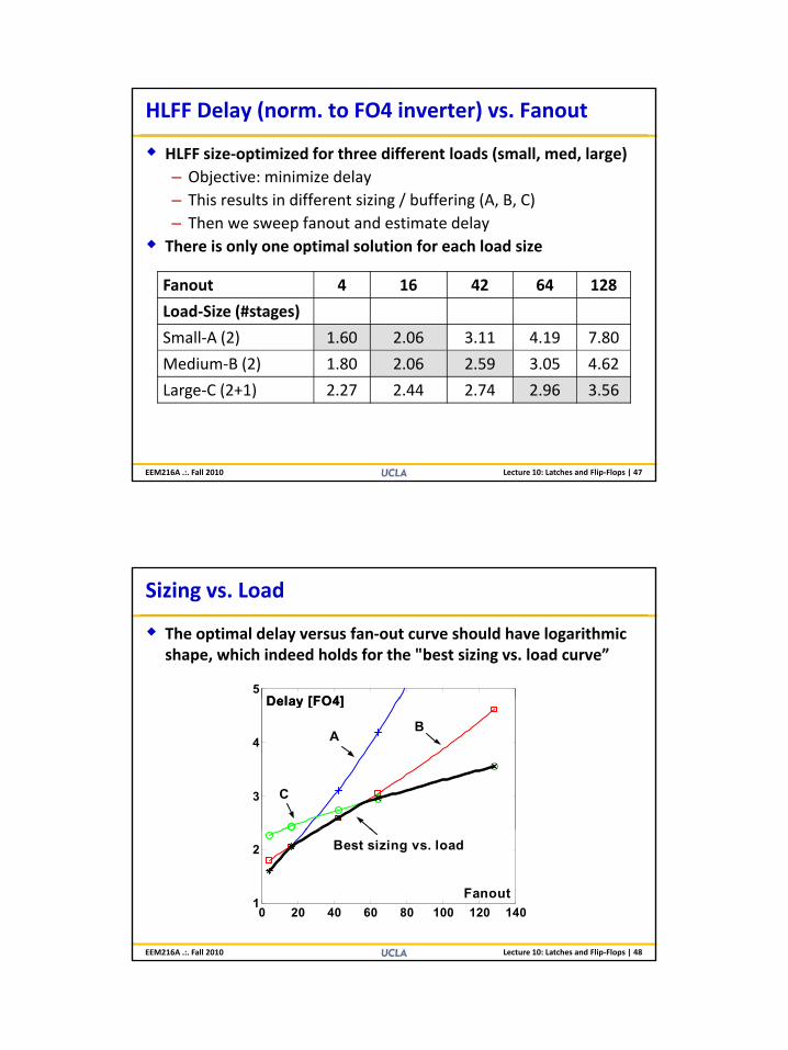
HLFF Delay (norm. to FO4 inverter) vs. Fanout
HLFF size‐optimized for three different loads (small, med, large)– Objective: minimize delay– This results in different sizing / buffering (A, B, C)
Th f t d ti t d l– Then we sweep fanout and estimate delayThere is only one optimal solution for each load size
Fanout 4 16 42 64 128
Load‐Size (#stages)
Small‐A (2) 1.60 2.06 3.11 4.19 7.80
D. Markovic / Slide 47EEM216A .:. Fall 2010 Lecture 10: Latches and Flip‐Flops | 47
Medium‐B (2) 1.80 2.06 2.59 3.05 4.62
Large‐C (2+1) 2.27 2.44 2.74 2.96 3.56
Sizing vs. Load
The optimal delay versus fan‐out curve should have logarithmic shape, which indeed holds for the "best sizing vs. load curve”
5Delay [FO4]Delay [FO4]
3
4
Delay [FO4] Delay [FO4]
A B
C
D. Markovic / Slide 48EEM216A .:. Fall 2010 Lecture 10: Latches and Flip‐Flops | 48
0 20 40 60 80 100 120 1401
2 Best sizing vs. load
Fanout
25
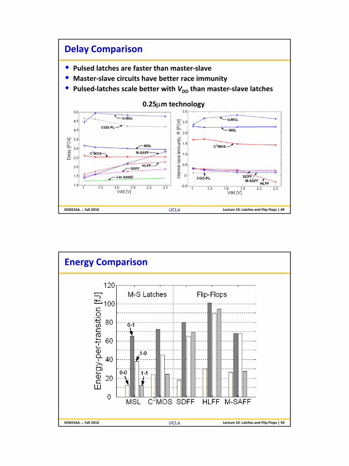
Delay Comparison
Pulsed latches are faster than master‐slaveMaster‐slave circuits have better race immunityPulsed‐latches scale better with VDD than master‐slave latches
0.25µm technology
D. Markovic / Slide 49EEM216A .:. Fall 2010 Lecture 10: Latches and Flip‐Flops | 49
Energy Comparison
D. Markovic / Slide 50Lecture 10: Latches and Flip‐Flops | 50EEM216A .:. Fall 2010
26
Summary
Clocks are a convenient constraint to simplify system design– Essentially forces delay of all logic paths to equal TClk
St l t b b ilt b ith (1) i itiStorage elements can be built by either (1) using positive feedback to keep the value or (2) using capacitance to dynamically store the value– Dynamic elements are faster but are less robust
Dynamic storage is sensitive to noise
D. Markovic / Slide 51
– Particularly charge injection and charge sharing
Lecture 10: Latches and Flip‐Flops | 51EEM216A .:. Fall 2010