0.15-µm Gallium Nitride (GaN) Microwave Integrated … · Army Research Laboratory Adelphi, MD...
18
0.15-μm Gallium Nitride (GaN) Microwave Integrated Circuit Designs Submitted to TriQuint Semiconductor for Fabrication by John Penn ARL-TN-0496 September 2012 Approved for public release; distribution unlimited.
Transcript of 0.15-µm Gallium Nitride (GaN) Microwave Integrated … · Army Research Laboratory Adelphi, MD...
0.15-µm Gallium Nitride (GaN) Microwave Integrated
Circuit Designs Submitted to TriQuint Semiconductor for
Fabrication
by John Penn
ARL-TN-0496 September 2012
Approved for public release; distribution unlimited.
NOTICES
Disclaimers
The findings in this report are not to be construed as an official Department of the Army position
unless so designated by other authorized documents.
Citation of manufacturer’s or trade names does not constitute an official endorsement or
approval of the use thereof.
Destroy this report when it is no longer needed. Do not return it to the originator.
Army Research Laboratory Adelphi, MD 20783-1197
ARL-TN-0496 September 2012
0.15-µm Gallium Nitride (GaN) Microwave Integrated
Circuit Designs Submitted to TriQuint Semiconductor for
Fabrication
John Penn
Sensors and Electron Devices Directorate, ARL
Approved for public release; distribution unlimited.
ii
REPORT DOCUMENTATION PAGE Form Approved
OMB No. 0704-0188 Public reporting burden for this collection of information is estimated to average 1 hour per response, including the time for reviewing instructions, searching existing data sources, gathering and maintaining the
data needed, and completing and reviewing the collection information. Send comments regarding this burden estimate or any other aspect of this collection of information, including suggestions for reducing the
burden, to Department of Defense, Washington Headquarters Services, Directorate for Information Operations and Reports (0704-0188), 1215 Jefferson Davis Highway, Suite 1204, Arlington, VA 22202-4302.
Respondents should be aware that notwithstanding any other provision of law, no person shall be subject to any penalty for failing to comply with a collection of information if it does not display a currently
valid OMB control number.
PLEASE DO NOT RETURN YOUR FORM TO THE ABOVE ADDRESS.
1. REPORT DATE (DD-MM-YYYY)
September 2012
2. REPORT TYPE
Final
3. DATES COVERED (From - To)
4. TITLE AND SUBTITLE
0.15-µm Gallium Nitride (GaN) Microwave Integrated Circuit Designs
Submitted to TriQuint Semiconductor for Fabrication
5a. CONTRACT NUMBER
5b. GRANT NUMBER
5c. PROGRAM ELEMENT NUMBER
6. AUTHOR(S)
John Penn
5d. PROJECT NUMBER
5e. TASK NUMBER
5f. WORK UNIT NUMBER
7. PERFORMING ORGANIZATION NAME(S) AND ADDRESS(ES)
U.S. Army Research Laboratory
ATTN: RDRL-SER-E
2800 Powder Mill Road
Adelphi, MD 20783-1197
8. PERFORMING ORGANIZATION REPORT NUMBER
ARL-TN-0496
9. SPONSORING/MONITORING AGENCY NAME(S) AND ADDRESS(ES)
10. SPONSOR/MONITOR'S ACRONYM(S)
11. SPONSOR/MONITOR'S REPORT NUMBER(S)
12. DISTRIBUTION/AVAILABILITY STATEMENT
Approved for public release; distribution unlimited.
13. SUPPLEMENTARY NOTES
14. ABSTRACT
High-speed electronic circuits are needed for Army systems in communications, wireless sensors, imaging, and other systems.
Gallium nitride (GaN) technology offers the highest power densities for radio frequency (RF) and wireless integrated circuits.
Several GaN broadband high power efficient power amplifier designs for high frequency operation, such as satellite
communications (SATCOM), were recently designed and submitted for fabrication using a proprietary 0.15-µm GaN process
under development at TriQuint Semiconductor. These monolithic microwave integrated circuits (MMICs) are being
fabricated by TriQuint as part of a recent cooperative research and development agreement (CRADA) with the U.S. Army
Research Laboratory (ARL).
15. SUBJECT TERMS
MMIC, GaN
16. SECURITY CLASSIFICATION OF:
17. LIMITATION OF ABSTRACT
UU
18. NUMBER OF PAGES
18
19a. NAME OF RESPONSIBLE PERSON
John Penn
a. REPORT
Unclassified
b. ABSTRACT
Unclassified
c. THIS PAGE
Unclassified
19b. TELEPHONE NUMBER (Include area code)
(301) 394-0423
Standard Form 298 (Rev. 8/98)
Prescribed by ANSI Std. Z39.18
iii
Contents
List of Figures iv
1. Introduction 1
2. Layout of GaN Die 1
3. Summary of Designs 3
4. Design Rule Checking (DRC) 4
5. Design Data Sheet 4
6. Conclusion 4
Appendix A. Checklist for 0.15 µm GaN Submission 7/20/2012 7
Appendix B. Customer Datasheet for 0.15 µm GaN Submission 7/20/2012 9
List of Symbols, Abbreviations, and Acronyms 11
Distribution List 12
iv
List of Figures
Figure 1. CKT1 30-/45-GHz PAs, plus a broadband LNA 2.5 mm x 2 mm. .................................2
Figure 2. CKT2 30-GHz Harmonic two way combiner PA 2.5 mm x 2 mm. ................................3
1
1. Introduction
Compact very efficient communication links are important to Army systems for
communications, wireless sensors, and other electronic systems. Constantly improving power
efficiencies, power densities, and higher bandwidths continue to push the state of the art in radio
frequency (RF) electronics and devices. Recent advances in gallium nitride (GaN) technology
have significantly increased power densities for monolithic microwave integrated circuits
(MMICs) over previous technologies, such as gallium arsenide (GaAs) and other III/V devices.
The U.S. Army Research Laboratory (ARL) is interested in custom design of circuits for state-
of-the-art systems and also state-of-the-art commercially available parts. TriQuint
Semiconductor is a provider of both foundry services for GaN custom MMICs as well as
commercial MMICs. A previous technical report; SATCOM and Ka-band Gallium Nitride
(GaN) Power Amplifier Monolithic Microwave Integrated Circuit (MMIC), ARL-MR-08171;
described several custom GaN broadband power amplifiers at Ka-band, to demonstrate high
efficiency, high-power power amplifiers (PAs) for microwave communications, applicable to
satellite communications (SATCOM). Two of those Ka-band designs were submitted to
TriQuint Semiconductor for fabrication under a recent cooperative research and development
agreement (CRADA) between ARL and TQS, Inc. Additional circuits by the author, John Penn,
and also by Caroline Waiyaiki of ARL, were submitted for fabrication and those designs will be
documented in later reports.
2. Layout of GaN Die
Several PAs for Ka-band and higher frequency operation were designed using TriQuint’s
proprietary 0.15-µm GaN process. Early access to this unreleased fabrication process was
obtained through the CRADA between ARL and TQS, Inc. TriQuint agreed to fabricate two
2.5 mm x 2 mm die, as these circuits are of mutual interest in obtaining high frequency, high
performance PAs for SATCOM and other communications systems with military applications.
Design was performed with computer-aided design (CAD) tools using models provided by TQS,
and using a design kit containing passive components from TriQuint’s lower frequency
commercial 0.25-µm GaN process, which are compatible with the 0.15-µm GaN process. These
circuits were then combined into two 2.5 mm x 2 mm die to comprise part of the tiling of
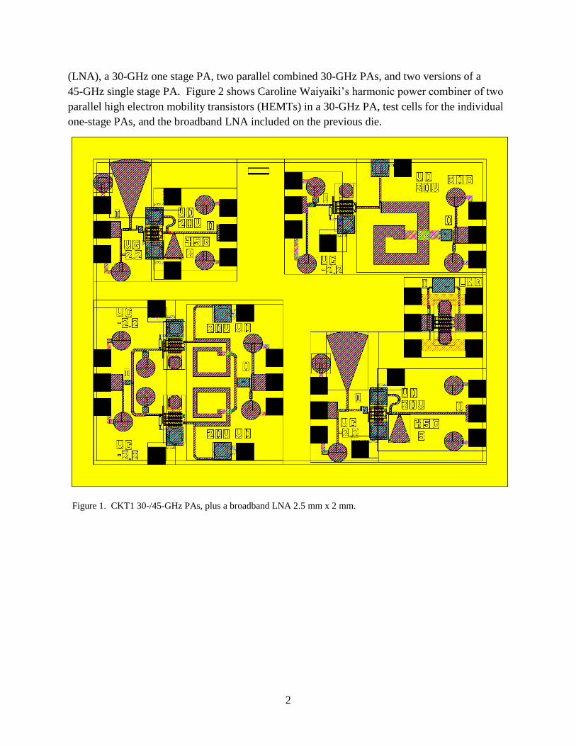
TriQuint’s next multi-project prototype 0.15-µm GaN wafer fabrication. Figure 1 shows the plot
of the first die layout, which includes a broadband high third-order intercept low-noise amplifier
1Penn, J. SATCOM and Ka-band Gallium Nitride (GaN) Power Amplifier Monolithic Microwave Integrated Circuit (MMIC);
ARL-MR-0817; U.S. Army Research Laboratory: Adelphi, MD, April 2012.
2
(LNA), a 30-GHz one stage PA, two parallel combined 30-GHz PAs, and two versions of a
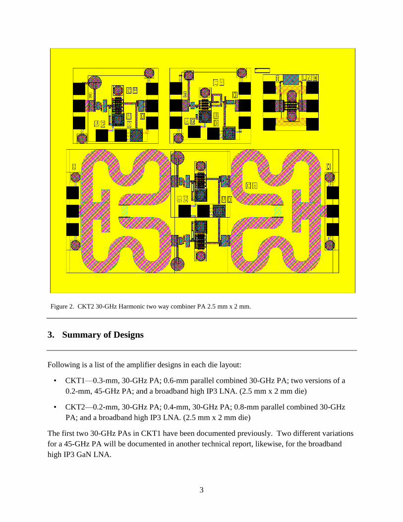
45-GHz single stage PA. Figure 2 shows Caroline Waiyaiki’s harmonic power combiner of two
parallel high electron mobility transistors (HEMTs) in a 30-GHz PA, test cells for the individual
one-stage PAs, and the broadband LNA included on the previous die.
Figure 1. CKT1 30-/45-GHz PAs, plus a broadband LNA 2.5 mm x 2 mm.
3
Figure 2. CKT2 30-GHz Harmonic two way combiner PA 2.5 mm x 2 mm.
3. Summary of Designs
Following is a list of the amplifier designs in each die layout:
• CKT1—0.3-mm, 30-GHz PA; 0.6-mm parallel combined 30-GHz PA; two versions of a
0.2-mm, 45-GHz PA; and a broadband high IP3 LNA. (2.5 mm x 2 mm die)
• CKT2—0.2-mm, 30-GHz PA; 0.4-mm, 30-GHz PA; 0.8-mm parallel combined 30-GHz
PA; and a broadband high IP3 LNA. (2.5 mm x 2 mm die)
The first two 30-GHz PAs in CKT1 have been documented previously. Two different variations
for a 45-GHz PA will be documented in another technical report, likewise, for the broadband
high IP3 GaN LNA.
4
Caroline Waiyaiki has been designing high linearity, efficient, high frequency amplifiers using a
harmonic termination power combiner passive circuit. The tradeoff is larger size in the combiner
versus improved linearity due to reduced higher order harmonics. Her doctoral thesis is based on
this harmonic power combiner circuit and those designs will be documented separately.
4. Design Rule Checking (DRC)
Design rule checking (DRC) verifies all the layout information to provide for manufacturability.
Checks for correct line widths, spacing between polygons within the masks, and checks for
appropriate combinations of layers, etc., to ensure a successful design are performed with the
DRC software and design rules—both provided by TriQuint. Initially, the layouts were checked
according to the process design rules supplied by TriQuint, but for their released 0.25-µm GaN
process. TriQuint provided additional DRC for the research 0.15-µm GaN process. Discussions
with a TriQuint layout engineer and modifications to the layout were performed to remove all
design rule errors. There still is the possibility of an electrical error, even with a correct DRC
check. No additional layout versus schematic checking was done for these designs, possibly that
will be available in the future. This is the first ARL submission in this unreleased TriQuint
0.15 µm GaN process.
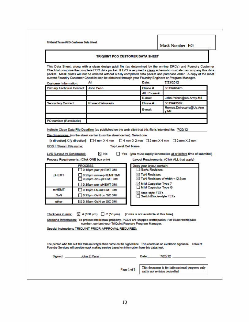
5. Design Data Sheet
TriQuint’s customer design data sheet must be completed and submitted along with the standard
GDSII layout file. The design checklist is completed to ensure that the tile design has passed
DRC checks and ensure the avoidance of common pitfalls. Any fabrication options are
designated such as 4-mil thinned wafers with substrate vias for this design. Lastly, plots of the
die layouts are included. This should match what TriQuint receives when they import the GDSII
file into their system.
6. Conclusion
ARL designed and submitted to fabrication several high efficiency, high power GaN Ka-band
PAs for SATCOM applications and other communications systems of interest to the Army.
TriQuint Semiconductor will fabricate these designs under the CRADA between ARL and TQS.
Once the designs are returned, they will be tested and documented in future reports. These will
be the first designs from ARL using early access to the high frequency 0.15-µm GaN research
process from TriQuint. Earlier broadband GaN amplifiers using TriQuint’s released 0.25-µm
5
GaN process are documented in ARL technical reports ARL-TR-59872, Broadband, Efficient,
Linear C-Band Power Amplifiers Designed in a 0.15 µm Gallium Nitride (GaN) Foundry
Process from TriQuint Semiconductor, April 2012. Testing of those devices is documented in a
coming technical report. Additional reports on the design of the 45-GHz PAs and broadband
LNA will be released. Likewise, Caroline Waiyaiki will document her thesis work on the
harmonic power combiner circuit for improved linearity in PA design.
2Penn, J. Broadband, Efficient, Linear C-Band Power Amplifiers Designed in a 0.15 µm Gallium Nitride (GaN) Foundry
Process from TriQuint Semiconductor; ARL-TR-5987; U.S. Army Research Laboratory: Adelphi, MD, April 2012.
6
INTENTIONALLY LEFT BLANK.
7
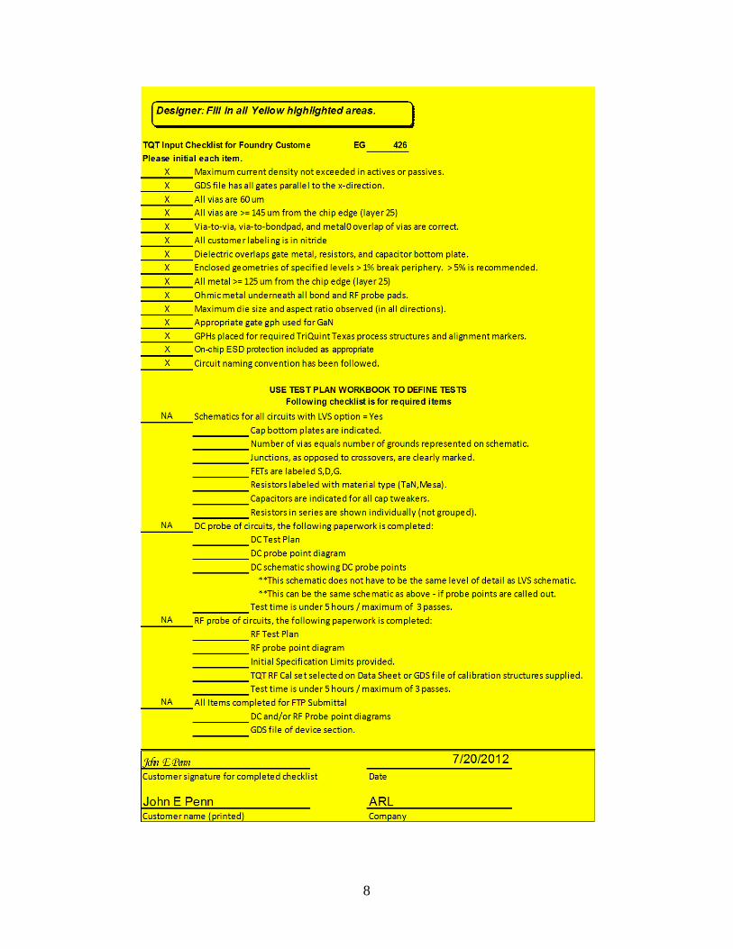
Appendix A. Checklist for 0.15 µm GaN Submission 7/20/2012
The following is the checklist for the 0.15-µm GaN submission, 7/20/2012.
8
Designer: Fill in all Yellow highlighted areas.
TQT Input Checklist for Foundry Custome
Please initial each item.
EG 426 ---X Maximum current density not exceeded in actives or passives.
X GDS file has all gates parallel to the x-direction.
X All vias are 60 um
X All vias are>= 145 um from the chip edge (layer 25)
X Via-to-via, via-to-bond pad, and metaiO overlap of vias are correct.
;..... l _..;.x;.__AII custome r labeli ng is in nitride
X Dielectric overlaps gate metal, resistors, and capacitor bottom plate.
X Enclosed geometries of specified levels > 1% break periphery. > 5% is recommended.
X All metal >= 125 um from the chip edge (layer 25)
X Ohmic metal underneath al l bond and RF probe pads.
X Maximum d ie size and aspect ratio observed (in all directions).
X Appropriate gate gph used for GaN
X GPHs placed for required TriQuint Texas process structures and alignment markers.
X On-chip ESD protection inc luded as appropriate
X Circuit naming convention has been follow ed.
USE TEST PLAN WORKBOOK TO DEFINE TESTS Following checklist is for required items
NA Schematics f or all circuits with LVS option = Yes
_____ Cap bottom plates are indicated.
_____ Number of vias equals number of grounds represented on schematic.
_____ Junctions, as opposed to crossovers, are clearly marked.
_____ FETs are labeled S,D,G.
_____ Resistors labeled with material type (TaN,Mesa).
_____ Capacitors are indicated for all cap t weakers.
_____ Resistors in series are shown individually (not grouped).
NA DC probe of circuits, the following paperwork is completed: _____ DC Test Plan
_____ DC probe point diagram
_____ DC schematic showing DC probe points
**This schematic does not have to be the same leve l of detail as LVS schematic.
**This can be the same schematic as above- if probe points are called out.
----Test time is under 5 hours I maximum of 3 passes.
NA RF probe of ci rcuits, the following paperwork is completed:
RFTest Plan ----_____ RF probe point diagram
_____ Initial Specifi cation Limits provided.
_____ TQT RF Cal se t se lected on Data Sheet or GDS file of calibration structures supplied.
_____ Test time is under 5 hours I maximum of 3 passes.
NA All Items completed for FTP Submittal
_____ DC and/or RF Probe point diagrams
GDS file of device section. ----
Customer signature for completed checklist Date
John E Penn ARL Customer name (printed) Company
7/20/2012
9
Appendix B. Customer Datasheet for 0.15 µm GaN Submission 7/20/2012
The following is the customer data sheet for the 0.15-µm GaN submission, 7/20/2012.
10
11
List of Symbols, Abbreviations, and Acronyms
ARL U.S. Army Research Laboratory
CAD computer-aided design
CRADA cooperative research and development agreement
DRC design rule checked
GaAs gallium arsenide
GaN gallium nitride
LNA low-noise amplifier
MMIC monolithic microwave integrated circuit
PA power amplifier
HEMT high electron mobility transistor
RF radio frequency
SATCOM satellite communications
TQS TriQuint Semiconductor, Inc.
12
1 DEFENSE TECHNICAL
(PDF INFORMATION CTR
only) DTIC OCA
8725 JOHN J KINGMAN RD
STE 0944
FORT BELVOIR VA 22060-6218
1 DIRECTOR
US ARMY RESEARCH LAB
IMAL HRA
2800 POWDER MILL RD
ADELPHI MD 20783-1197
1 DIRECTOR
US ARMY RESEARCH LAB
RDRL CIO LL
2800 POWDER MILL RD
ADELPHI MD 20783-1197
1 DIRECTOR
US ARY RESEARCH LAB
RDRL CIO LT
2800 POWDER MILL RD
ADELPHI MD 20783-1197
12 DIRECTOR
US ARMY RESEARCH LAB
RDRL SER
PAUL AMIRTHARAJ
RDRL SER E
ROMEO DEL ROSARIO
BEN HUEBSCHMAN
JAMES WILSON
TONY IVANOV
JOHN PENN (3 HCS)
ROBERT PROIE
ROBERT REAMS
PANKAJ SHAH
ED VIVEIROS
2800 POWDER MILL RD
ADELPHI MD 20783-1197