0 Multi-Port Memory Controller (MPMC) (v4.02.a)Multi-Port Memory Controller (MPMC) (v4.02.a) 2 DS643...
164
DS643 June 28, 2008 www.xilinx.com 1 Product Specification © Copyright 2002 – 2008 Xilinx, Inc. All Rights Reserved. XILINX, the Xilinx logo, the Brand Window and other designated brands included herein are trademarks of Xilinx, Inc. The PowerPC name and logo are registered trademarks of IBM Corp., and used under license. All other trademarks are the property of their respective owners. Xilinx is providing this design, code, or information (collectively, the “Information”) to you “AS IS” with no warranty of any kind, express or implied. Xilinx makes no representation that the Information, or any particular implementation thereof, is free from any claims of infringement. You are responsible for obtaining any rights you may require for any implementation based on the Information. XILINX EXPRESSLY DISCLAIMS ANY WARRANTY WHATSOEVER WITH RESPECT TO THE ADEQUACY OF THE INFORMATION OR ANY IMPLEMENTATION BASED THEREON, INCLUDING BUT NOT LIMITED TO ANY WARRANTIES OR REPRESENTATIONS THAT THIS IMPLEMENTATION IS FREE FROM CLAIMS OF INFRINGEMENT AND ANY IMPLIED WARRANTIES OF MERCHANTABILITY OR FITNESS FOR A PARTICULAR PURPOSE. Except as stated herein, none of the Information may be copied, reproduced, dis- tributed, republished, downloaded, displayed, posted, or transmitted in any form or by any means including, but not limited to, electronic, mechanical, photocopying, recording, or otherwise, without the prior written consent of Xilinx. Introduction MPMC is a fully parameterizable memory controller that supports SDRAM/DDR/DDR2 memory. MPMC provides access to memory for one to eight ports, where each port can be chosen from a set of Personality Inter- face Modules (PIMs) that permit connectivity into PowerPC® 405 processor and MicroBlaze™ processors using CoreConnect® PLBv4.6 and the MPMC Native Port Interface (NPI) structures, and well as a a Memory Interface Block (MIB) PIM (PPC440MC) for the Pow- erPC 440 Processor. MPMC supports the Soft Direct Memory Access (SDMA) controller that provides full-duplex, high-bandwidth, LocalLink interfaces into memory. A Video Frame Buffer Controller (VFBC) PIM is also available. Additionally, MPMC supports optional Error Correcting Code (ECC) and Performance Monitoring (PM). Features • Soft Direct Memory Access (SDMA) support. • Double Data Rate (DDR/DDR2) and Single Data Rate (SDR) SDRAM memory support. • DIMM support (registered and unbuffered). • Error Correcting Code (ECC) support. • Parameterizable number of ports (1 to 8). • Parameterizable number of data bits to memory (8, 16, 32, 64) and parameterizable configuration of data path FIFOs. • Performance Monitoring (PM) support. • Memory Interface Generator (MIG)-based PHY v.2.1 support. • Static Physical (PHY) interface alternative to the MIG-based PHY. • User configuration of arbitration algorithms. • Customizeable Interfaces: Xilinx CacheLink (XCL), LocalLink (using SDMA), Processor Local Bus (PLB v4.6) with Xilinx simplifications, Native Port Interface (NPI), MIB/PPC440MC, and VFBC. Note: This document uses the terms “PLB v4.6” and “PLB” to refer to PLB v4.6 with Xilinx simplifications. MPMC does not support earlier versions of PLB (such as PLB v3.4). Also note that MPMC does not directly connect to OPB peripherals; such connection would require a PLB v4.6 to OPB or an OPB to PLB v4.6 bridge.’See "Reference Documents" page 163 for more information about this bus standard and about the migration of designs to use this standard. 0 Multi-Port Memory Controller (MPMC) (v4.02.a) DS643 June 28, 2008 0 0 Product Specification LogiCORE Facts Core Specifics Supported Device Family (1) Virtex™-II Pro, Spartan™-3 (includes: Spartan-3, Spartan-3A,Spartan-3E, Spartan-3AN, and Spartan-3ADSP including Automotive Devices), Virtex-4, Virtex-5 Resources Used I/O LUTs FFs Block RAMs n n n n Provided with Core Documentation DS643 Multi-Port Memory Controller (MPMC) Data Sheet (this document) Design File Formats Verilog/VHDL Reference Designs Application Notes See “Reference Documents,” page 163 Design Tool Requirements Xilinx® Implementation Tools ISE™ 10.1or later as required by EDK Verification ModelSim PE 6.3d Simulation ModelSim PE 6.3d Synthesis Xilinx Synthesis Technology (XST) Support Provided by Xilinx, Inc. 1. Throughout this document all mention of Spartan-3 devices or families includes the automotive version of the devices. The auto- motive devices are treated the same as the equivalent non-auto- motive device. For example the “spartan3a” families are treated as the same.
Transcript of 0 Multi-Port Memory Controller (MPMC) (v4.02.a)Multi-Port Memory Controller (MPMC) (v4.02.a) 2 DS643...

© Copyright 2002 – 2008 Xilinx, Inc. All Rights Reserved.
IntroductionMPMC is a fully parameterizable memory controller that supports SDRAM/DDR/DDR2 memory. MPMC provides access to memory for one to eight ports, where each port can be chosen from a set of Personality Inter-face Modules (PIMs) that permit connectivity into PowerPC® 405 processor and MicroBlaze™ processors using CoreConnect® PLBv4.6 and the MPMC Native Port Interface (NPI) structures, and well as a a Memory Interface Block (MIB) PIM (PPC440MC) for the Pow-erPC 440 Processor. MPMC supports the Soft Direct Memory Access (SDMA) controller that provides full-duplex, high-bandwidth, LocalLink interfaces into memory. A Video Frame Buffer Controller (VFBC) PIM is also available. Additionally, MPMC supports optional Error Correcting Code (ECC) and Performance Monitoring (PM).
Features• Soft Direct Memory Access (SDMA) support.
• Double Data Rate (DDR/DDR2) and Single Data Rate (SDR) SDRAM memory support.
• DIMM support (registered and unbuffered).
• Error Correcting Code (ECC) support.
• Parameterizable number of ports (1 to 8).
• Parameterizable number of data bits to memory (8, 16, 32, 64) and parameterizable configuration of data path FIFOs.
• Performance Monitoring (PM) support.
• Memory Interface Generator (MIG)-based PHY v.2.1 support.
• Static Physical (PHY) interface alternative to the MIG-based PHY.
• User configuration of arbitration algorithms.
• Customizeable Interfaces: Xilinx CacheLink (XCL), LocalLink (using SDMA), Processor Local Bus (PLB v4.6) with Xilinx simplifications, Native Port Interface (NPI), MIB/PPC440MC, and VFBC.
Note: This document uses the terms “PLB v4.6” and “PLB” to refer to PLB v4.6 with Xilinx simplifications. MPMC does not support earlier versions of PLB (such as PLB v3.4). Also note that MPMC does not directly connect to OPB peripherals; such connection would require a PLB v4.6 to OPB or an OPB to PLB v4.6 bridge.’See "Reference Documents" page 163 for more information about this bus standard and about the migration of designs to use this standard.
0
Multi-Port Memory Controller(MPMC) (v4.02.a)
DS643 June 28, 2008 0 0 Product Specification
LogiCORE Facts
Core Specifics
Supported Device Family(1)
Virtex™-II Pro, Spartan™-3(includes: Spartan-3,
Spartan-3A,Spartan-3E, Spartan-3AN, andSpartan-3ADSP including Automotive
Devices), Virtex-4, Virtex-5
Resources Used
I/O LUTs FFsBlock RAMs
n n n n
Provided with Core
DocumentationDS643 Multi-Port Memory Controller(MPMC) Data Sheet (this document)
Design File Formats
Verilog/VHDL
Reference Designs Application Notes
See “Reference Documents,” page 163
Design Tool Requirements
Xilinx® Implementation Tools
ISE™ 10.1or later as required by EDK
Verification ModelSim PE 6.3d
Simulation ModelSim PE 6.3d
Synthesis Xilinx Synthesis Technology (XST)
Support
Provided by Xilinx, Inc.
1. Throughout this document all mention of Spartan-3 devices or families includes the automotive version of the devices. The auto-motive devices are treated the same as the equivalent non-auto-motive device. For example the “spartan3a” families are treated as the same.
DS643 June 28, 2008 www.xilinx.com 1Product Specification
XILINX, the Xilinx logo, the Brand Window and other designated brands included herein are trademarks of Xilinx, Inc. The PowerPC name and logo are registered trademarks of IBM Corp., and used under license. All other trademarks are the property of their respective owners.
Xilinx is providing this design, code, or information (collectively, the “Information”) to you “AS IS” with no warranty of any kind, express or implied. Xilinx makes no representation that the Information, or any particular implementation thereof, is free from any claims of infringement. You are responsible for obtaining any rights you may require for any implementation based on the Information. XILINX EXPRESSLY DISCLAIMS ANY WARRANTY WHATSOEVER WITH RESPECT TO THE ADEQUACY OF THE INFORMATION OR ANY IMPLEMENTATION BASED THEREON, INCLUDING BUT NOT LIMITED TO ANY WARRANTIES OR REPRESENTATIONS THAT THIS IMPLEMENTATION IS FREE FROM CLAIMS OF INFRINGEMENT AND ANY IMPLIED WARRANTIES OF MERCHANTABILITY OR FITNESS FOR A PARTICULAR PURPOSE. Except as stated herein, none of the Information may be copied, reproduced, dis-tributed, republished, downloaded, displayed, posted, or transmitted in any form or by any means including, but not limited to, electronic, mechanical, photocopying, recording, or otherwise, without the prior written consent of Xilinx.

Multi-Port Memory Controller (MPMC) (v4.02.a)
Design ParametersThe following tables provide the design parameters, allowable values, and descriptions for the MPMC system, associated memory, and Personality Interface Modules (PIMs). Parameter values that are strings or that contain alpha-numeric characters must be uppercase.
MPMC System Parameters
Table 1: MPMC System Parameters
Parameter NameDefault Value
Allowable Values
Description
C_ALL_PIMS_SHARE_ADDRESSES (1) 1 0,1
Specifies whether MPMC ports use the C_MPMC_BASEADDR and C_MPMC_HIGHADDR for address decoding or all ports have independent address range decoding. Also specifies whether SDMA control register interfaces use the C_SDMA_CTRL_BASEADDR and C_SDMA_CTRL_HIGHADDR for address decoding or MPMC ports and SDMA control register ports have independent address range decoding.1 = MPMC ports use C_MPMC_BASEADDR and C_MPMC_HIGHADDR for address decoding; SDMA control registers use C_SDMA_CTRL_BASEADDR and C_SDMA_CTRL_HIGHADDR.0 = MPMC ports and SDMA control registers have independent address range decoding.
C_ARB_PIPELINE 1 0,1Enables or disables the Arbiter Pipeline:0 = Disable Arbiter Pipeline.1 = Enable Arbiter Pipeline. (performance)
C_ARB_USE_DEFAULT 0 0Default Arbitration Algorithm to use (unimplemented).
C_ARB0_ALGO ROUND_ROBINROUND_ROBIN, FIXED, CUSTOM
String that specifies the arbitration scheme to use for Algorithm 0 (Custom will consume a block RAM). Only valid if C_NUM_PORTS > 1.
C_ARB0_NUM_SLOTS 1 1-16Number of time slots to use for Custom Algorithm. Only valid if C_ARBO_ALGO = CUSTOM.
C_ARB0_SLOT0C_ARB0_SLOT1C_ARB0_SLOT2C_ARB0_SLOT3C_ARB0_SLOT5C_ARB0_SLOT6C_ARB0_SLOT7C_ARB0_SLOT8C_ARB0_SLOT9C_ARB0_SLOT10C_ARB0_SLOT11C_ARB0_SLOT12C_ARB0_SLOT13C_ARB0_SLOT14C_ARB0_SLOT15
NONEString of Numbers,
Example: “01234567”
Arbitration Priority for Time Slot n where n is 0-15, and the number of valid Time Slots is from 0 to (C_ARB0_NUM_SLOTS-1). Left to right, highest to lowest priority. Every valid port must be specified once only.Only valid if C_ARBO_ALGO = CUSTOM.
C_DEBUG_REG_ENABLE 0 0,1 Reserved
2 www.xilinx.com DS643 June 28, 2008Product Specification

Multi-Port Memory Controller (MPMC) (v4.02.a)
C_FAMILY virtex5 STRING
Targeted FPGA device family. Options are:
• spartan3(a/e/an/adsp) = Spartan-3 family
• aspartan3(a/e/an/adsp) = Automotive Spartan3 family
• virtex2p = Virtex-II Pro
• virtex4 = Virtex-4
• virtex5 = Virtex-5
C_SUBFAMILY “fx” STRING
When targeting Virtex-4 or Virtex-5 device platforms:
• “fx” = fx or fxt
• “lx” = lx or lxt
• “sx” = sx or sxtThis parameter is not user settable and is only used for internal Design Rule Checks (DRC). Value is set to “” for all other families.
C_IDELAYCTRL_LOC (5) NOT_SET STRINGIDELAYCTRL constraint locations (Hyphen separated).
C_MAX_REQ_ALLOWED 1 1 Number of requests MPMC can queue per port.
C_MPMC_BASEADDR(1) 0xFFFFFFFF Valid Address MPMC PIMs Shared Base Address.
C_MPMC_HIGHADDR (1) 0x00000000 Valid Address MPMC PIMs Shared High Address.
C_MPMC_CTRL_BASEADDR 0xFFFFFFFF Valid Address
MPMC CTRL PLB v4.6 Base Address. Only valid if Performance Monitors (PM), Error Correction Code (ECC), or Static PHY is enabled. Must be 64K aligned.
C_MPMC_CTRL_HIGHADDR 0x00000000 Valid AddressMPMC CTRL PLB v4.6 High Address. Only valid if PM, ECC, or Static PHY is enabled.
C_MPMC_CTRL_AWIDTH 32 32PLB v4.6 Address Width. Only valid if PM, ECC, or Static PHY is enabled.
C_MPMC_CTRL_DWIDTH 64 32,64,128PLB v4.6 Data Width. Only valid if PM, ECC, or Static PHY is enabled.
C_MPMC_CTRL_NATIVE_DWIDTH 32 32PLB v4.6 Native Data Width. Only valid if PM, ECC, or Static PHY is enabled.
C_MPMC_CTRL_PLB_NUM_MASTERS 1 0-16PLB v4.6 Number of masters on the Bus. Only valid if PM, ECC, or Static PHY is enabled.
C_MPMC_CTRL_PLB_MID_WIDTH 1 0-4PLB v4.6 Master ID Width. Only valid if PM, ECC, or Static PHY is enabled.
C_MPMC_CTRL_P2P 1 0,1PLB v4.6 Point-To-Point (P2P) support. Only valid if PM, ECC, or Static PHY is enabled.
C_MPMC_CTRL_SUPPORT_BURSTS 0 0,1PLB v4.6 PIM Burst Support. Only valid if PM, ECC, or Static PHY is enabled.
C_MPMC_CTRL_SMALLEST_MASTER 32 32,64,128PLB v4.6 Smallest Master on Bus. Only valid if PM, ECC, or Static PHY is enabled.
C_NUM_IDELAYCTRL (5) 1 0- 16 Number of IDELAYCTRL elements to instantiate.
Table 1: MPMC System Parameters (Continued)
Parameter NameDefault Value
Allowable Values
Description
3 www.xilinx.com DS643 June 28, 2008Product Specification

Multi-Port Memory Controller (MPMC) (v4.02.a)
C_NUM_PORTS 1 1-8
Number of Interface Ports. MPMC GUI automatically sets the value and places the correct parameter in the Microprocessor Hardware Specification (MHS) file.
C_PIM<Port_Num>_BASETYPE (4) 2 (Port 0)0 (Ports 1-7)
0 - 6
0 = INACTIVE1 = XCL 2 = PLB v4.63 = SDMA4 = NPI5 = PPC440MC6 = VFBC
C_PIM<Port_Num>_SUBTYPE x
IXCL, DXCL, XCL, DPLB, IPLB, PLB,
SDMA, NPI, PPC440MC, VFBC,
INACTIVE
Specific Port Interface Type. MPMC GUI sets the value automatically and places the correct parameter in the MHS file. This value is an automatically calculated parameter that can be overwritten; if set by user, it is not auto-calculated.
C_PM_ENABLE 0 0,1Performance Monitor (PM) enable or disable:1 = Enable0 = Disable
C_PM_DC_WIDTH (2) 48 1- 64 Sets the width of the PM dead cycle counters
C_PM_GC_CNTR (2) 1 0,1Global Clock Counter enable or disable:1 = Enable0 = Disable
C_PM_GC_WIDTH (2) 48 1- 64 Sets the width of the PM Global Cycle counter.
C_PM_SHIFT_CNT_BY (2) 1 0-3Specifies the size of the histogram bins used by the Performance Monitors.
C_RD_DATAPATH_TML_MAX_FANOUT 0 0,1,2,4,8
Read Database Timing Management Logic Maximum Register Fanout.Controls the fanout of the PHY layer to the read FIFO data path:0 = no register is instantiated.1 = the read data is forwarded from the PHY to eight sets of registers, then forwarded on to each of the read FIFOs.2 = the read data is forwarded from the PHY to four sets of registers. The outputs of the registers are the forwarded on to a maximum of two read FIFOs1.
4 = the read data is forwarded from the PHY to two sets of registers. The outputs of the registers are the forwarded on to a maximum of four read FIFOs1.
8 = the read data is forwarded from the PHY to a single register. The output of the register is forwarded on to a maximum of eight read FIFOs.
Note:1. Values of 3, 5, 6, 7 are invalid.
C_SKIP_SIM_INIT_DELAY 0 0,1For simulation only, allows a shorter initialization sequence.
C_STATIC_PHY_RDDATA_CLK_SEL (3) 0 0,1Sets power-on or reset value of RDDATA_CLK_SEL register.
Table 1: MPMC System Parameters (Continued)
Parameter NameDefault Value
Allowable Values
Description
4 www.xilinx.com DS643 June 28, 2008Product Specification

Multi-Port Memory Controller (MPMC) (v4.02.a)
C_STATIC_PHY_RDDATA_SWAP_RISE (3) 0 0,1Sets power-on or reset value of RDDATA_SWAP_RISE register.
C_STATIC_PHY_RDEN_DELAY (3) 5 0-15Sets power-on or reset value of RDENDELAY register.
C_SPECIAL_BOARD NONE
S3E_STKIT,S3E_1600E,S3A_STKIT,
NONE
Xilinx® special physical layer for Spartan-3x boards.
C_USE_STATIC_PHY 0 0,1
Enables or disables a software controlled interface for the physical layer calibration (Static PHY):0 = Static PHY Disabled.1 = Static PHY Enabled.
C_WR_DATAPATH_TML_PIPELINE 1 0,1
Enables or disables the Write Data Path Timing Management:0 = Write Data Path Timing Management Logic Pipeline Disabled.1 = Write Data Path Timing Management Logic Pipeline Enabled.
C_WR_TRAINING_PORT (5) 0 0-7
Specifies the port where the Write FIFO will be used for memory initialization. This value is an automatically calculated parameter that can be over-written. If the parameter is set by the user, it is not calculated.
Notes:1. When C_ALL_PIMS_SHARE_ADDRESSES is set to 1, C_MPMC_BASEADDR is used for all ports for memory access addressing and
C_SDMA_CTRL_BASEADDR is used for all SDMA PIMs (if applicable). If set to 0, the C_PIMx_BASEADDR, and C_SDMA_CTRLx_BASEADDR parameters are used.
2. Valid if C_PM_ENABLE is set to 1.3. Valid when using Static PHY (C_USE_STATIC_PHY = 1 or C_FAMILY = virtex2p).4. C_PIM<Port_Num>_BASETYPE must be set to 0 for unused ports that are outside the number active ports specified by C_NUM_PORTS.
For example, if C_NUM_PORTS = 4, then C_PIM4_BASETYPE, C_PIM5_BASETYPE, C_PIM6_BASETYPE, and C_PIM7_BASETYPE must all be 0.5. Valid when using MIG-based Virtex-4/Virtex-5 DDR/DDR2 PHY.
Table 1: MPMC System Parameters (Continued)
Parameter NameDefault Value
Allowable Values
Description
5 www.xilinx.com DS643 June 28, 2008Product Specification

Multi-Port Memory Controller (MPMC) (v4.02.a)
MPMC Per-port Parameters
The parameters in the following table are inside the MPMC core and can be set on a per-port basis.
Table 2: MPMC Per-port Parameters
Parameter NameDefault Value
Allowable Values
Description
C_PIM<Port_Num>_BASEADDR (1,7) 0xFFFFFFFF Valid Address PIM Base Address.
C_PIM<Port_Num>_HIGHADDR (1,8) 0x00000000 Valid Address PIM High Address.
C_PIM<Port_Num>_OFFSET (1) 0x00000000 Valid Address PIM Offset Address.
C_PI<Port_Num>_RD_FIFO_TYPE BRAMBRAM, SRL, DISABLED
Read Data Path FIFO type.
C_PI<Port_Num>_WR_FIFO_TYPE (6) BRAMBRAM, SRL,DISABLED
Write Data Path FIFO type.
C_PI<Port_Num>_ADDRACK_PIPELINE (3) 1 0,1 AddrAck Pipeline enable.
C_PI<Port_Num>_RD_FIFO_APP_PIPELINE 1 0,1 Read FIFO Port Side pipeline.
C_PI<Port_Num>_RD_FIFO_MEM_PIPELINE (4) 1 0,1 Read FIFO Memory Side pipeline.
C_PI<Port_Num>_WR_FIFO_APP_PIPELINE 1 0,1 Write FIFO Port Side pipeline.
C_PI<Port_Num>_WR_FIFO_MEM_PIPELINE (5) 1 0,1 Write FIFO Memory Side pipeline.
C_PI<Port_Num>_PM_USED (2,3) 1 0,1 Enable Performance Monitor
C_PI<Port_Num>_PM_DC_CNTR (2) 1 0,1 Enable Dead Cycle Counter
Notes:1. Only valid if C_PIM_BASETYPE is not 4 (NPI) and C_ALL_PIMS_USE_SHARED_ADDRESSES is 0.2. Only valid if C_PM_ENABLE = 1.3. If C_PM<Port_Num>_PM_USED is set to 1, then C_PI<Port_Num>_ADDRACK_PIPELINE must be set to 1 to monitor correctly.4. C_PI<Port_Num>_RD_FIFO_MEM_PIPELINE settings must all be the same from port 0 to port <C_NUM_PORTS-1>.
For example, on a four port design ports 0 to 3 must have the same C_PI<Port_Num>_RD_FIFO_MEM_PIPELINE settings.5. C_PI<Port_Num>>_WR_FIFO_MEM_PIPELINE settings must all be the same from port 0 to port <C_NUM_PORTS-1>.
For example, on a four port design ports 0 to 3 must have the same C_PI<Port_Num>_WR_FIFO_MEM_PIPELINE settings.6. Write FIFOs are automatically disabled in an MPMC port that is an IXCL or IPLB subtype. There is no need to manually disable write FIFOs in an IXCL
or IPLB configured port.7. C_PIM<Port_Num>_BASEADDR+C_PIM<Port_Num>_OFFSET represents the base physical memory address that the corresponding port is allowed
to access.For example, if C_PIM<Port_Num>_OFFSET is 0x00000000, C_PIM<Port_Num>_BASEADDR will represent the physical address of memory. If your total memory size is 0x03FFFFFF, a C_PIM_<Port_Num>_BASEADDR value of 0x00000000 will go to physical address 0x00000000. A value of 0x01000000 will go to physical address 0x01000000. A value of 0x04000000 will go to physical address 0x00000000.If you increase the C_PIM_<Port_Num>_OFFSET to 0x02000000, a C_PIM_<Port_Num>_BASEADDR value of 0x00000000 will go to physical ad-dress 0x02000000. A value of 0x01000000 will go to physical address 0x03000000. A value of 0x04000000 will go to physical address 0x02000000.
8. C_PIM<Port_Num>_HIGHADDR+C_PIM<Port_Num>_OFFSET represents the high physical memory address that the corresponding port is allowed to access.
6 www.xilinx.com DS643 June 28, 2008Product Specification

Multi-Port Memory Controller (MPMC) (v4.02.a)
Personality Interface Module (PIM) Parameters
XCL Design Parameters
PLB v4.6 PIM Design Parameters
Table 3: XCL Design Parameters
Parameter NameDefault Value
Allowable Values
Description
C_XCL<Port_Num>_LINESIZE (1) 4 1,4,8,16 Number of words per transaction.
C_XCL<Port_Num>PIPE_STAGES 3 0-3
Number of pipelines to include: 0 = No pipelines.1 = Include 1 pipeline.2 = Include 2 pipelines.3 = Include 3 pipelines.
C_XCL<Port_Num>_WRITEXFER(1) 1 0, 1, 2
XCL write transfer type:0 = No write transfers.1 = Single write transfers only.2 = Cacheline transfer only.
1. Valid when C_PIM<Port_Num>_BASETYPE = 1 (XCL) only
Table 4: PLB v4.6 Design Parameters
Parameter NameDefault Value
Allowable Values
Description
C_SPLB<Port_Num>_AWIDTH(2,3) 32 32 PLB Least Significant Address Bus Width.
C_SPLB<Port_Num>_DWIDTH(2,3) 64 32,64,128 Width of the PLB Data Bus.
C_SPLB<Port_Num>_NATIVE_DWIDTH(2) 64 32,64 Width of the PIM Internal Data Bus.
C_SPLB<Port_Num>_PLB_NUM_MASTERS(2,3) 1 1-16 Number of masters that can be connected the PIM.
C_SPLB<Port_Num>_PLB_MID_WIDTH(1,2,3) 1 0- 4
PLB Master ID Width. PLB Master ID Bus Width.The value is log2 (C_SPLB<Port_Num>_PLB_NUM_MASTERS) with a minimum value of 1.
C_SPLB<Port_Num>_P2P(2,3) 1 0,1
Selects Shared Bus or Point-to-Point (P2P) configuration for the PLB slave port:0 = PLB Shared Bus Connection.1 = PLB P2P Connection.Must be set to 1 when C_PIM<Port_Num>_SUBTYPE is set to IPLB or DPLB.
C_SPLB<Port_Num>_SUPPORT_BURSTS (2,3) 0 0,1PLB PIM Burst Support:0 = Single Word transactions.1 = Single, cacheline, and burst transactions.
C_SPLB<Port_Num>_SMALLEST_MASTER (2,3) 32 32,64,128 Width of the smallest Master Data Bus.
1. log2 represents a logarithm function of base 2. For example, log2(1)=0, log2(2)=1, log2(4)=2, log2(8)=3, log2(16)=4, etc.2. Valid if C_PIM<Port_Num>_BASETYPE = 2 (SPLB)3. These parameters are normally calculated by the XPS based on what devices are connected to the PLB bus.
7 www.xilinx.com DS643 June 28, 2008Product Specification

Multi-Port Memory Controller (MPMC) (v4.02.a)
SDMA Design Parameters
NPI Design Parameters
Table 5: SDMA Design Parameters
Parameter Name Default ValueAllowable
ValuesDescription
C_SDMA_CTRL_BASEADDR(1,2) 0xFFFFFFFF Valid AddressSDMA CTRL Shared PLB v4.6 Base Address.
C_SDMA_CTRL_HIGHADDR(1,2) 0x00000000 Valid AddressSDMA CTRL Shared PLB v4.6 High Address.
C_SDMA_CTRL<Port_Num>_BASEADDR (1,2) 0xFFFFFFFF Valid Address SDMA CTRL PLB Base Address.
C_SDMA_CTRL<Port_Num>_HIGHADDR (1,2) 0x00000000 Valid Address SDMA CTRL PLB High Address.
C_SDMA_CTRL<Port_Num>_AWIDTH (1,3) 32 32 PLB Address Width.
C_SDMA_CTRL<Port_Num>_DWIDTH (1,3) 64 32,64,128 PLB Data Width.
C_SDMA_CTRL<Port_Num>_NATIVE_DWIDTH (1,3) 32 32 PLB Native Data Width.
C_SDMA_CTRL<Port_Num>_PLB_NUM_MASTERS (1,3) 1 0-16 PLB Number of masters on the Bus.
C_SDMA_CTRL<Port_Num>_PLB_MID_WIDTH (1,3) 1 0-4 PLB Master ID Width.
C_SDMA_CTRL<Port_Num>_P2P (1,3) 1 0,1PLB Point-to-Point (P2P) support:0 = Not Supported.1 = Supported.
C_SDMA_CTRL<Port_Num>_SUPPORT_BURSTS (1,3) 0 0PLB PIM Burst support:0 = Not Supported.1 = Supported.
C_SDMA_CTRL<Port_Num>_SMALLEST_MASTER (1,3) 32 32,64,128 PLB Smallest Master on Bus.
C_SDMA<Port_Num>_PRESCALAR (1) 100 0-1023 Interrupt Delay Timer Scale Factor.
C_SDMA<Port_Num>_PI2LL_CLK_RATIO( 1) 1 1,2 NPI to LocalLink Clock ratio.
C_SDMA<Port_Num>_COMPLETED_ERR_TX (1) 1 0,1Transmit complete with error checking. 0 = Disable complete bit error checking.1 = Enable complete bit error checking.
C_SDMA<Port_Num>_COMPLETED_ERR_RX (1) 1 0,1Receive complete with error checking. 0 = Disable complete bit error checking.1 = Enable complete bit error checking.
Notes:1. Valid if C_PIM<Port_Num>_BASETYPE = 3 (SDMA)2. If C_ALL_PIMS_USED_SHARED_ADDRESS is 1, there is one common BASEADDR/HIGHADDR for all SDMAs (C_SDMA_CTRL_BASEADDR); other-
wise, each SDMA Port has a unique BASE/HIGHADDR (C_SDMA_CTRL<Port_Num>_BASEADDR).3. These parameters are normally calculated by the XPS based on what devices are connected to the PLB bus.
Table 6: NPI Design Parameters
Parameter NameDefault Value
Allowable Values
Description
C_PIM<Port_Num>_DATA_WIDTH 64 32,64 PIM Native Data Width.
8 www.xilinx.com DS643 June 28, 2008Product Specification

Multi-Port Memory Controller (MPMC) (v4.02.a)
MIB/PPC440MC Design Parameters
VFBC PIM Design Parameters
Table 7: MIB/PPC440MC Design Parameters
Parameter NameDefault Value
Allowable Values
Description
C_PPC440MC<Port_Num>_BURST_LENGTH 4 2,4,8 Length of allowable bursts.
C_PPC440MC<Port_Num>_PIPE_STAGES 1 0-2 Number of pipeline stages to insert.
Table 8: VFBC Design Parameters
Parameter NameDefaultValue
Allowable Values Description
C_VFBC<Port_Num>_ CMD_FIFO_DEPTH 32 1 - x (1) Depth of the command FIFO in 32-bit words.
C_VFBC<Port_Num>_CMD_AFULL_COUNT 30 -
C_VFBC<Port_Num>_ CMD_FIFO_DEPTH
Command FIFO almost full threshold.
C_VFBC<Port_Num>_RDWD_FIFO_DEPTH 1024 1 - x (1)Read/Write FIFO depth in the number of data words (word size is defined by the RDWD_DATA_WIDTH parameter).
C_VFBC<Port_Num>_RDWD_DATA_WIDTH 32 8,16,32,64 Data width in number of bits.
C_VFBC<Port_Num>_RD_AEMPTY_WD_AFULL_COUNT
30 -
C_VFBC<Port_Num>_ RDWD_FIFO_DEPTH
Write FIFO Almost Full Threshold and Read FIFO Almost Empty Threshold.
1. As the FIFO depth for each FIFO is increased, the FIFO consumes more block RAMs. The upper limit is constrained by the number of block RAMs available on the FPGA device and the number of block RAMS used.
9 www.xilinx.com DS643 June 28, 2008Product Specification

Multi-Port Memory Controller (MPMC) (v4.02.a)
Memory and Memory Part Parameters
Table 9: Memory and Memory Part Parameters
Parameter NameDefault Value
Allowable Values
Description
C_MEM_TYPE DDR2DDR, DDR2,
SDRAMMemory architecture type.
C_MEM_PARTNO (1) NONE
Database Part Number, Example:
“mt4htf3264h-53e”, CUSTOM
Specifies the memory part number from database or CUSTOM.
C_MEM_PART_DATA_DEPTH (1) 161, 2, 4, 8, 16, 32, 128, 256,
512, 1024Discrete memory part data depth.
C_MEM_PART_DATA_WIDTH (1) 16 8,16, 32, 64 Discrete memory part data width.
C_MEM_PART_NUM_BANK_BITS (1) 2 1–4 Number of bank bits on memory part.
C_MEM_PART_NUM_ROW_BITS (1) 13 1–20 Number of row bits on memory part.
C_MEM_PART_NUM_COL_BITS (1) 9 1–20 Number of column bits on memory part.
C_MEM_PART_TRAS (1) x Any Integer tRAS - Minimum ACTIVE-to-PRECHARGE command (ps).
C_MEM_PART_TRASMAX (1) x Any Integer tRAS - Maximum ACTIVE-to-PRECHARGE command (ps).
C_MEM_PART_TRC (1) x Any IntegertRC - Minimum ACTIVE-to-ACTIVE (same bank) command (ps).
C_MEM_PART_TRCD (1) x Any Integer tRCD - Minimum ACTIVE-to-READ or WRITE delay (ps).
C_MEM_PART_TDQSS (1,2) 1 1tDQSS - Positive DQS latching edge to associated clock edge (tCK). This value should be (maximum value - minimum value) rounded up to the nearest integer.
C_MEM_PART_TWR (1) x Any Integer tWR - Minimum write recover time (ps).
C_MEM_PART_TRP (1) x Any Integer tRP - Minimum PRECHARGE command period (ps).
C_MEM_PART_TMRD (1) x Any Integer tMRD - Minimum LOAD MODE command cycle time (tCK).
C_MEM_PART_TRRD (1) x Any IntegertRRD - Minimum ACTIVE bank a to ACTIVE bank b command (ps).
C_MEM_PART_TRFC (1) x Any IntegertRFC - Minimum REFRESH to ACTIVE or REFRESH to REFRESH command interval (ps).
C_MEM_PART_TREFI (1) x Any Integer tREFI - Maximum average periodic REFRESH interval (ps).
C_MEM_PART_TAL (1,3) 0 0 tAL - Additive Latency desired (tCK).
C_MEM_PART_TCCD (1,3) x Any Integer tCCD - Minimum CAS# to CAS# command delay (tCK).
10 www.xilinx.com DS643 June 28, 2008Product Specification

Multi-Port Memory Controller (MPMC) (v4.02.a)
C_MEM_PART_TWTR (1,3) x Any IntegertWTR - Minimum internal WRITE-to-READ command delay (ps).
C_MEM_PART_TRTP (1,3) 7500 7500tRTP - Minimum internal READ to PRECHARGE command delay (ps).
C_MEM_PART_CAS_A_FMAX (1,4) x Any Integer Maximum Frequency for the lowest CAS latency.
C_MEM_PART_CAS_A (1,4) x Any Integer Lowest CAS latency for this memory part.
C_MEM_PART_CAS_B_FMAX (1,4) x Any IntegerMaximum Frequency for the next lowest CAS latency (if applicable).
C_MEM_PART_CAS_B (1,4) x Any IntegerNext Lowest CAS latency for this memory part (if applicable).
C_MEM_PART_CAS_C_FMAX (1,4) x Any IntegerMaximum Frequency for the next lowest CAS latency (if applicable).
C_MEM_PART_CAS_C (1,4) x Any IntegerNext Lowest CAS latency for this memory part (if applicable).
C_MEM_PART_CAS_D_FMAX(1,4) x Any IntegerMaximum Frequency for the next lowest CAS latency (if applicable).
C_MEM_PART_CAS_D (1,4) x Any IntegerNext Lowest CAS latency for this memory part (if applicable).
Memory Parameters
C_MEM_DQS_IO_COL x any 18-bit value
Only used with MIG-based Virtex-5 DDR2 PHY. See “MIG-based PHY Design and Implementation Considerations for Spartan-3 and Virtex-5 DDR2,” page 43 for more information on setting this value.
C_MEM_DQ_IO_MS0x00000000000000
0000any 72-bit value
Only used with MIG-based Virtex-5 DDR2 PHY. See “MIG-based PHY Design and Implementation Considerations for Spartan-3 and Virtex-5 DDR2,” page 43 for more information on setting this value.
C_MEM_CAS_LATENCY0(5) 0 0–9 Auto-calculated Memory CAS latency based on Clk Speed.
C_MEM_ODT_TYPE (3) 0 0, 1, 2, 3
On-Die Termination Setting (DDR2 only):0 = Disabled1 = 75 Ohms2 = 150 Ohms3 = Reserved/50 Ohms
C_MEM_REDUCED_DRV 0 0,1 Reduced drive output enable.
C_MEM_REG_DIMM 0 0,1 DIMM is registered.
C_MPMC_CLK0_PERIOD_PS 10000 1-1000000 MPMC_CLK0 Period (ps).
Table 9: Memory and Memory Part Parameters (Continued)
Parameter NameDefault Value
Allowable Values
Description
11 www.xilinx.com DS643 June 28, 2008Product Specification

Multi-Port Memory Controller (MPMC) (v4.02.a)
C_MEM_CLK_WIDTH 1 1-16Number of external clock pins. This value is an automatically calculated parameter that can be overwritten; if set by the user, it is not calculated.
C_MEM_ODT_WIDTH(3) 1 1-16
Number of external ODT Pins. This value is an automatically calculated parameter that can be overwritten; if set by the user, it is not calculated. This must be set to an integer multiple of C_NUM_RANKS * C_NUM_DIMMS.
C_MEM_CE_WIDTH 1 1-16Number of external chip enable pins. This value is an automatically calculated parameter that can be overwritten; if set by the user, it is not calculated.
C_MEM_CS_N_WIDTH 1 1-16
Number of external chip select pins. This value is an automatically calculated parameter that can be overwritten; if set by the user, it is not calculated. This must be set to an integer multiple of C_NUM_RANKS * C_NUM_DIMMS.
C_MEM_ADDR_WIDTH 13 1-20 Number of external address pins.
C_MEM_BANKADDR_WIDTH 2 1-4 Number of external bank address pins.
C_MEM_DATA_WIDTH 64 8,16,32,64 Number of external data pins.
C_MEM_BITS_DATA_PER_DQS 8 8 Number of data bits per DQS bit.
C_MEM_DM_WIDTH 8 1,2,4,8 Number of external data mask pins.
C_MEM_DQS_WIDTH(2,3) 8 1,2,4,8 Number of external DQS pins.
C_MEM_NUM_DIMMS 1 1Number of DIMMs. Set to 1 if not using a DIMM. Multiple DIMMS are not supported.
C_MEM_NUM_RANKS(7) 1 1-2 Number of ranks per DIMM. A value of 2 is not recommended.
Notes:1. These values are auto-updated from the IP Configurator database if C_MEM_PARTNO is set to a part number from the database. If set to CUSTOM,
the values must be filled in according to the memory parameters provided by the manufacturer. Unlisted parts can be requested for future versions by opening a Xilinx support WebCase and attaching the new memory datasheet.The database is a Comma Separated Value (CSV) file located at <MPMC pcore location>/data/mpmc_memory_database.csv.
2. DDR Parameter.3. DDR2 Parameter.4. CAS latencies/Fmax pairs should be arranged from Lowest CAS Latency and Slowest Frequency to Highest CAS Latency and Fastest frequency
for pairs A-D.5. Non-user, auto-calculated value.6. Valid if C_INCLUDE_ECC_SUPPORT is enabled.7. The use of Multi-Rank designs is strongly discouraged.
See the “MIG-Based PHY Design Considerations,” page 42 for more information.
Table 9: Memory and Memory Part Parameters (Continued)
Parameter NameDefault Value
Allowable Values
Description
12 www.xilinx.com DS643 June 28, 2008Product Specification

Multi-Port Memory Controller (MPMC) (v4.02.a)
Table 9: Additional Memory and Memory Part Parameters (Continued)
Parameter NameDefault Value
Allowable Values
Description
Additional Part Parameters
C_DDR2_DQSN_ENABLE (3) 1 0,1
Enables differential DQS (DDR2 Only). Must be set to 0 when C_FAMILY = “spartan3”. (Can be set to 1 for other Spartan3x families such as spartan3a, spartan3an, spartan3adsp, spartan3e)Must be set to 1 when using MIG-based Virtex-5 DDR2 PHY.
C_INCLUDE_ECC_SUPPORT 0 0,1Enables ECC logic. ECC control registers are accessible from MPMC_CTRL interface when enabled.
C_ECC_DEFAULT_ON (6) 1 0,1 Enables ECC enable register at RST:
C_INCLUDE_ECC_TEST (6) 0 0,1Enable or disable ECC Test Functionality and registers:1 = Enable ECC test functionality/registers.0 = No ECC test functionality (saves area).
C_ECC_SEC_THRESHOLD (6) 1 0-4095 Single-bit data error interrupt threshold counter value.
C_ECC_DEC_THRESHOLD (6) 1 0-4095 Double-bit data error interrupt threshold counter value.
C_ECC_PEC_THRESHOLD (6) 1 0-4095Specifies the parity-bit data error interrupt threshold counter value.
C_ECC_DATA_WIDTH (5,6) 0 0, 3-8 ECC Data Width (in Bits).
C_ECC_DM_WIDTH (5,6) 0 0,1 ECC DM Width.
C_ECC_DQS_WIDTH (5,6) 0 0,1 ECC DQS width.
Notes:1. These values are auto-updated from the IP Configurator database if C_MEM_PARTNO is set to a part number from the database. If set to CUSTOM,
the values must be filled in according to the memory parameters provided by the manufacturer. Unlisted parts can be requested for future versions by opening a Xilinx support WebCase and attaching the new memory datasheet.The database is a Comma Separated Value (CSV) file located at <MPMC pcore location>/data/mpmc_memory_database.csv.
2. DDR Parameter.3. DDR2 Parameter.4. CAS latencies/Fmax pairs should be arranged from Lowest CAS Latency and Slowest Frequency to Highest CAS Latency and Fastest frequency for
pairs A-D.5. Non-user, auto-calculated value.6. Valid if C_INCLUDE_ECC_SUPPORT is enabled.
13 www.xilinx.com DS643 June 28, 2008Product Specification

Multi-Port Memory Controller (MPMC) (v4.02.a)
MPMC I/O SignalsThe following tables provide the I/O signals for the MPMC system, memory, and PIMs.
System I/O Signals
Table 10: System I/O Signals
Signal Name DirectionInit
StatusDescription
MPMC_Clk0 Input x System clock input.
MPMC_Clk90 Input x System clock input, phase shifted by 90 degrees.
MPMC_Clk0_DIV2 Input xMPMC_Clk0, divided by 2, clock input. Only valid when using MIG-based Virtex-5 DDR2 PHY.
MPMC_Clk_200MHz (1) Input x200 MHz clock. Connects to IDELAY elements and does not have to be phase or frequency related to MPMC_Clk0. Valid only when using MIG-based Virtex-4/Virtex-5 DDR/DDR2 PHY.
MPMC_Rst Input x System reset input.
MPMC_Clk_Mem (2) Input xMemory read data capture clock used by Static PHY; otherwise should be left unconnected
MPMC_Idelayctrl_Rdy_I (1) InputAutomatically set to 1 if unconnected
This active high input is combined with internal IDELAYCTRL_RDY signals to indicate that the memory initialization can begin.
MPMC_Idelayctrl_Rdy_0 (1) Output 0This active high output signals that the internal IDELAYCTRL RDY signals and the MPMC_Ideleayctrl_Rdy_I are all high.
MPMC_InitDone Output 0This active high signal, when asserted, indicates that the memory initialization has completed successfully. When LOW, the memory is currently being calibrated and configured.
MPMC_ECC_Intr Output 0ECC Interrupt: (level sensitive) 1 = Interrupt asserted.0 = No Interrupt.
MPMC_DCM_PSEN (2) Output xConnects to PSEN pin of DCM to allow MPMC Static PHY to change DCM phase.
MPMC_DCM_PSINCDEC (2) Output xConnects to PSINCDEC pin of DCM to allow MPMC Static PHY to change DCM phase.
MPMC_DCM_PSDONE (2) Input xConnects to PSDONE pin of DCM to allow MPMC Static PHY to change DCM phase.
1. Signals are applicable MIG-based Virtex-4/Virtex-5 DDR/DDR2 PHY only.2. Signals are applicable when using Static PHY only.
14 www.xilinx.com DS643 June 28, 2008Product Specification

Multi-Port Memory Controller (MPMC) (v4.02.a)
Memory Signals
SDRAM PHY I /O Signals
Double Data Rate (DDR) and Double Data Rate 2 (DDR2) I/O Signals
DDR I/O Signals
Table 11: SDRAM PHY I/O Signals
Signal DirectionInit
StatusDescription
SDRAM_Clk Output 0 Clock to memory.
SDRAM_CE Output 0 Clock enable. (memory CKE signal)
SDRAM_CS_n Output 1 Chip select, active-low.
SDRAM_RAS_n Output 1 Command input.
SDRAM_CAS_n Output 1 Command input.
SDRAM_WE_n Output 1 Command input.
SDRAM_BankAddr Output x Bank address.
SDRAM_Addr Output x Row/Column address.
SDRAM_DQ(1) In/Out z Data bits.
SDRAM_DM Output 0 Data masks.
1. The MHS signal connecting this port and the MHS external port must have the same name. See http://www.xilinx.com/support/answers/14264.htm. The “Reference Documents,” page 163 has a link to this topic.
Table 12: DDR I/O Signals
Signal Name(1) Direction Init Status Description
DDR_Clk Output 0 Clock to memory.
DDR_Clk_n Output 1 Inverted clock to memory.
DDR_CE Output 0 1 = Clock enabled. (memory CKE signal)
DDR_CS_n Output 1 0 = Chip select enabled.
DDR_RAS_n Output 1 Command input.
DDR_CAS_n Output 1 Command input.
DDR_WE_n Output 1 Command input.
DDR_BankAddr Output x Bank address.
DDR_Addr Output x Row/Column address.
DDR_DQ (3) In/Out x Data.
DDR_DM Output x Data mask outputs.
DDR_DQS (3) In/Out x Data strobe.
DDR_DQS_DIV_O (2) Output x Timing loop signal.
DDR_DQS_DIV_I (2) Input x Timing loop signal.
1. For detailed signal descriptions, refer to device-specific data sheets.2. Required when using MIG-based Spartan-3 (3/3A/3AN/3ADSP/3E) PHY.3. The MHS signal connecting this port and the MHS external port must have the same name. See http://www.xilinx.com/support/answers/14264.htm.
The “Reference Documents,” page 163 has a link to this topic.
15 www.xilinx.com DS643 June 28, 2008Product Specification

Multi-Port Memory Controller (MPMC) (v4.02.a)
DDR2 I/O Signals
Table 13: DDR2 I/O Signals
Signal Name(1) Direction Init Status Description
DDR2_Clk Output 0 Clock to memory.
DDR2_Clk_n Output 1 Inverted clock to memory.
DDR2_CE Output 0 1 = Clock enabled.
DDR2_CS_n Output 1 0 = Chip select enabled.
DDR2_RAS_n Output 1 Command input.
DDR2_CAS_n Output 1 Command input.
DDR2_WE_n Output 1 Command input.
DDR2_BankAddr Output x Bank address.
DDR2_Addr Output x Row/Column address.
DDR2_DQ(3) In/Out x Data.
DDR2_DM Output x Data mask outputs.
DDR2_DQS (3) In/Out x Data Strobe.
DDR2_DQS_n (4) In/Out x Inverted Data Strobe.
DDR2_DQS_DIV_O (2) Output x Timing loop signal.
DDR2_DQS_DIV_I (2) Input x Timing loop signal.
DDR2_ODT Output 0
On-Die-Termination signal. Care must be taken when connecting these pins to your memory when you have more than one rank; there is a direct relationship to the DDR2_CS_n pins.
1. For detailed signal descriptions, refer to device-specific data sheets.2. Required when using MIG-based Spartan-3/3A/3AN/3ADSP/3E DDR/DDR2 PHY.3. The MHS signal connecting this port and the MHS external port must have the same name. See http://www.xilinx.com/support/answers/14264.htm.
The “Reference Documents,” page 163 has a link to this topic.4. Required when differential DQS is enabled (C_DDR2_DQSN_ENABLE = 1).
16 www.xilinx.com DS643 June 28, 2008Product Specification

Multi-Port Memory Controller (MPMC) (v4.02.a)
PIM I/O Signals
XCL PIM I/O Signals
PLB v4.6, SDMA_CTRL, and MPMC_CTRL PIM I/O Signals
MPMC contains Slave PLB ports for the PLB PIM, SDMA Control Registers (SDMA_CTRL), and MPMC Control Reg-ister (MPMC_CTRL) interfaces. Each of these slave PLB interfaces have the same set of signal names with different prefixes on the Port Bus Names. The <Bus_Name> prefixes are as follows:
• SDMA Control Registers (SDMA_CTRL) for Ports 0 to 7: SDMA_CTRL<Port_Num>_
- SDMA_CTRL is valid if C_PIM<Port_Num>_BASETYPE = 3
• MPMC Control Registers (MPMC_CTRL): MPMC_CTRL
- MPMC_CTRL is valid if PM, ECC, or Static PHY is enabled
• MPMC Slave PLB v4.6 PIM: SPLB<Port_Num>
- SPLB<Port_Num> is valid if C_PIM<Port_Num>_BASETYPE = 2
The following table lists the available signals for SDMA_CTRL, MPMC_CTRL, and PLB v4.6 PIM (SPLB). Replace <Bus_Name> with the appropriate bus prefix.
Table 14: XCL PIM I/O Signals
Signal Name DirectionInit
StatusDescription
FSL<Port_Num>_M_Clk Input x Clock
FSL<Port_Num>_M_Write Input x Write enable signal indicating that data is being written to the output FSL.
FSL<Port_Num>_M_Data Input x Data value written to the output FSL.
FSL<Port_Num>_M_Control Input x Control bit value written to the output FSL.
FSL<Port_Num>_M_Full Output 0 Full Bit indicating output FSL FIFO is full when set.
FSL<Port_Num>_S_Clk Input x Clock
FSL<Port_Num>_S_Read Input xRead acknowledge signal indicating that data has been read from the input FSL.
FSL<Port_Num>_S_Data Output x Data value currently available at the top of the input FSL.
FSL<Port_Num>_S_Control Output 0 Control Bit value currently available at the top of the input FSL.
FSL<Port_Num>_S_Exists Output 0 Flag indicating that data exists in the input FSL.
Table 15: SDMA_CTRL, MPMC_CTRL, and PLB v4.6 (SPLB) PIM I/O Signals
Signal Name DirectionInit
StatusDescription
<Bus_Name>_Clk Input x Bus Clock.
<Bus_Name>_Rst Input x PLB reset, active high.
<Bus_Name>_PLB_ABus Input x PLB address bus.
<Bus_Name>_PLB_PAValid Input x PLB primary address valid.
<Bus_Name>_PLB_SAValid Input x PLB secondary address valid.
<Bus_Name>_PLB_masterID Input x PLB current master identifier.
<Bus_Name>_PLB_RNW Input x PLB read not write.
17 www.xilinx.com DS643 June 28, 2008Product Specification

Multi-Port Memory Controller (MPMC) (v4.02.a)
<Bus_Name>_PLB_BE Input x PLB byte enables.
<Bus_Name>_PLB_UABus Input x PLB size of requested transfer.
<Bus_Name>_PLB_rdPrim Input x PLB secondary to primary read request indicator.
<Bus_Name>_PLB_wrPrim Input x PLB secondary to primary write request indicator.
<Bus_Name>_PLB_abort Input x PLB abort bus request.
<Bus_Name>_PLB_busLock Input x PLB bus lock.
<Bus_Name>_PLB_MSize Input x PLB data bus width indicator.
<Bus_Name>_PLB_size Input x PLB size of requested transfer.
<Bus_Name>_PLB_type Input x PLB transfer type.
<Bus_Name>_PLB_lockErr Input x PLB lock error indicator.
<Bus_Name>_PLB_wrPendReq Input x PLB pending write bus request indicator.
<Bus_Name>_PLB_wrPendPri Input x PLB pending write request priority.
<Bus_Name>_PLB_rdPendReq Input x PLB read bus request indicator.
<Bus_Name>_PLB_rdPendPri Input x PLB read bus request priority.
<Bus_Name>_PLB_reqPri Input x PLB current request priority.
<Bus_Name>_PLB_TAttribute Input x PLB transfer attribute bus.
<Bus_Name>_PLB_rdBurst Input x PLB read burst transfer indicator.
<Bus_Name>_PLB_wrBurst Input x PLB burst write transfer indicator.
<Bus_Name>_PLB_wrDBus Input x PLB write data bus.
<Bus_Name>_Sl_addrAck Output 0 Slave address acknowledge.
<Bus_Name>_Sl_SSize Output 0 Slave data bus size.
<Bus_Name>_Sl_wait Output 0 Slave wait indicator.
<Bus_Name>_Sl_rearbitrate Output 0 Slave rearbiitrate bus indicator.
<Bus_Name>_Sl_wrDAck Output 0 Slave write data acknowledge.
<Bus_Name>_Sl_wrComp Output 0 Slave write transfer complete indicator.
<Bus_Name>_Sl_wrBTerm Output 0 Slave terminate write burst transfer.
<Bus_Name>_Sl_rdDBus Output 0 Slave read data bus.
<Bus_Name>_Sl_rdWdAddr Output 0 Slave read word address.
<Bus_Name>_Sl_rdDAck Output 0 Slave read data acknowledge.
<Bus_Name>_Sl_rdComp Output 0 Slave read transfer complete indicator.
<Bus_Name>_Sl_rdBTerm Output 0 Slave terminate read burst transfer.
<Bus_Name>_Sl_MBusy Output 0 Slave busy indicator.
<Bus_Name>_Sl_MRdErr Output 0 Slave read error indicator.
<Bus_Name>_Sl_MWrErr Output 0 Slave write error indicator.
<Bus_Name>_Sl_MIRQ Output 0 Slave interrupt indicator.
Table 15: SDMA_CTRL, MPMC_CTRL, and PLB v4.6 (SPLB) PIM I/O Signals (Continued)
Signal Name DirectionInit
StatusDescription
18 www.xilinx.com DS643 June 28, 2008Product Specification

Multi-Port Memory Controller (MPMC) (v4.02.a)
SDMA LocalLink I/O Signals
Table 16: SDMA LocalLink Interface Signals
Signal Name DirectionInit
StatusDescription
LocalLink System Interface
SDMA<Port_Num>_Clk Input x LLink_Clk
Transmit LocalLink Interface
SDMA<Port_Num>_TX_D(31:0) Output 0 Transmit LocalLink Data Bus.
SDMA<Port_Num>_TX_Rem(3:0) Output 1 Transmit LocalLink Remainder Bus.
SDMA<Port_Num>_TX_SOF Output 1 Transmit LocalLink Start of Frame.
SDMA<Port_Num>_TX_EOF Output 1 Transmit LocalLink End of Frame.
SDMA<Port_Num>_TX_SOP Output 1 Transmit LocalLink Start of Payload.
SDMA<Port_Num>_TX_EOP Output 1 Transmit LocalLink End of Payload.
SDMA<Port_Num>_TX_Src_Rdy Output 1 Transmit LocalLink Source Ready.
SDMA<Port_Num>_TX_Dst_Rdy Input x Transmit LocalLink Destination Ready.
Receive LocalLink Interface
SDMA<Port_Num>_RX_D(31:0) Input x Receive LocalLink Data Bus.
SDMA<Port_Num>_RX_Rem(3:0) Input x Receive LocalLink Remainder Bus.
SDMA<Port_Num>_RX_SOF Input x Receive LocalLink Start of Frame.
SDMA<Port_Num>_RX_EOF Input x Receive LocalLink End of Frame.
SDMA<Port_Num>_RX_SOP Input x Receive LocalLink Start of Payload.
SDMA<Port_Num>_RX_EOP Input x Receive LocalLink End of Payload.
SDMA<Port_Num>_RX_Src_Rdy Input x Receive LocalLink Source Ready.
SDMA<Port_Num>_RX_Dst_Rdy Output 1 Receive LocalLink Destination Ready.
SDMA System Interface
SDMA<Port_Num>_RxIntOut Output 0 Receive interrupt output.
SDMA<Port_Num>_TxIntOut Output 0 Transmit interrupt output.
SDMA<Port_Num>_RstOut Output 0 Soft Reset Acknowledge.
19 www.xilinx.com DS643 June 28, 2008Product Specification
Multi-Port Memory Controller (MPMC) (v4.02.a)
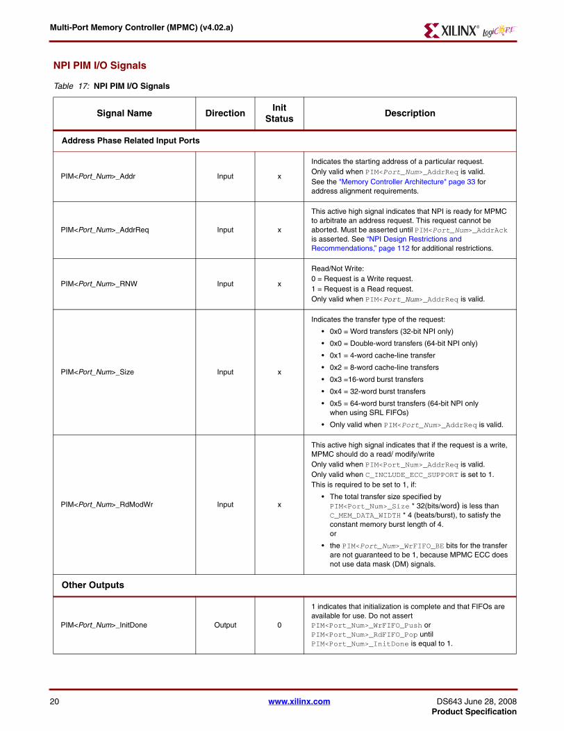
NPI PIM I/O Signals
Table 17: NPI PIM I/O Signals
Signal Name DirectionInit
StatusDescription
Address Phase Related Input Ports
PIM<Port_Num>_Addr Input x
Indicates the starting address of a particular request. Only valid when PIM<Port_Num>_AddrReq is valid.See the "Memory Controller Architecture" page 33 for address alignment requirements.
PIM<Port_Num>_AddrReq Input x
This active high signal indicates that NPI is ready for MPMC to arbitrate an address request. This request cannot be aborted. Must be asserted until PIM<Port_Num>_AddrAck is asserted. See “NPI Design Restrictions and Recommendations,” page 112 for additional restrictions.
PIM<Port_Num>_RNW Input x
Read/Not Write:0 = Request is a Write request.1 = Request is a Read request.Only valid when PIM<Port_Num>_AddrReq is valid.
PIM<Port_Num>_Size Input x
Indicates the transfer type of the request:
• 0x0 = Word transfers (32-bit NPI only)
• 0x0 = Double-word transfers (64-bit NPI only)
• 0x1 = 4-word cache-line transfer
• 0x2 = 8-word cache-line transfers
• 0x3 =16-word burst transfers
• 0x4 = 32-word burst transfers
• 0x5 = 64-word burst transfers (64-bit NPI only when using SRL FIFOs)
• Only valid when PIM<Port_Num>_AddrReq is valid.
PIM<Port_Num>_RdModWr Input x
This active high signal indicates that if the request is a write, MPMC should do a read/ modify/writeOnly valid when PIM<Port_Num>_AddrReq is valid.Only valid when C_INCLUDE_ECC_SUPPORT is set to 1.This is required to be set to 1, if:
• The total transfer size specified by PIM<Port_Num>_Size * 32(bits/word) is less than C_MEM_DATA_WIDTH * 4 (beats/burst), to satisfy the constant memory burst length of 4. or
• the PIM<Port_Num>_WrFIFO_BE bits for the transfer are not guaranteed to be 1, because MPMC ECC does not use data mask (DM) signals.
Other Outputs
PIM<Port_Num>_InitDone Output 0
1 indicates that initialization is complete and that FIFOs are available for use. Do not assert PIM<Port_Num>_WrFIFO_Push or PIM<Port_Num>_RdFIFO_Pop until PIM<Port_Num>_InitDone is equal to 1.
20 www.xilinx.com DS643 June 28, 2008Product Specification

Multi-Port Memory Controller (MPMC) (v4.02.a)
Address Phase Related Output Ports
PIM<Port_Num>_AddrAck Output 0
This active high signal indicates that MPMC has begun arbitration for address request. Valid for one cycle of MPMC_Clk0.PIM<Port_Num>_AddrReq must be deasserted on the next cycle of MPMC_Clk0 unless NPI is requesting a new transfer.
Write Data Phase Related Input Ports
PIM<Port_Num>_WrFIFO_Data Input xData to be pushed into MPMC write FIFOs.Only valid with PIM<Port_Num>_WrFIFO_Push.Data is little-endian as shown in Figure 7 on page 54.
PIM<Port_Num>_WrFIFO_BE Input xIndicates which bytes of PIM<Port_Num>_WrFIFO_Data to write. Only valid with PIM<Port_Num>_WrFIFO_Push.
PIM<Port_Num>_WrFIFO_Push Input x
This active high signal indicates push PIM<Port_Num>_WrFIFO_Data into write FIFOs.Must be asserted for one cycle of MPMC_Clk0.Cannot be asserted while PIM<Port_Num>_InitDone is 0. Cannot be asserted while PIM<Port_Num>_WrFIFO_AlmostFull is asserted.Can be asserted before, after, or during the address phase unless MPMC is configured in one of several special cases.See the "NPI Design Restrictions and Recommendations" page 112.
PIM<Port_Num>_WrFIFO_Flush Input x Reserved. Drive with 0.
Write Data Phase Related Output Ports
PIM<Port_Num>_WrFIFO_Empty Output 1This active high signal indicates that there are less than C_MEM_DATA_WIDTH bits of data in the write FIFO.
PIM<Port_Num>_WrFIFO_AlmostFull Output 0
This active high signal indicates that PIM<Port_Num>_WrFIFO_Push cannot be asserted on the next cycle of MPMC_Clk0. This signal is only asserted when using SRL FIFOs. If BRAM FIFOs are used, the PIM cannot allow more than 1024 bytes of data to be pushed into the FIFOs.
Read Data Phase Related Input Ports
PIM<Port_Num>_RdFIFO_Pop Input x
This active high signal indicates that read FIFO fetch the next value of PIM<Port_Num>_RdFIFO_Data.Must be asserted for one cycle of MPMC_Clk0.Cannot be asserted while PIM<Port_Num>_InitDone is 0.Cannot be asserted while PIM<Port_Num>_RdFIFO_Empty is asserted.See information in PIM<Port_Num>_RdFIFO_RdFIFO_Latency to know when PIM<Port_Num>_RdFIFO_Data is valid.
Table 17: NPI PIM I/O Signals (Continued)
Signal Name DirectionInit
StatusDescription
21 www.xilinx.com DS643 June 28, 2008Product Specification

Multi-Port Memory Controller (MPMC) (v4.02.a)
PIM<Port_Num>_RdFIFO_Flush Input x
This active high signal indicates that the read FIFO flags should be reset.Must be asserted for one cycle of MPMC_Clk0.
Caution! Only assert this signal when PIM_<Port_Num>_RdFIFO_Empty is deasserted to prevent problems with the read FIFO address counters. If it is asserted when multiple read address re-quests are acknowledged, but where the data phases corre-sponding to the address phases have not completed, there is a possibility that MPMC is, or will be, in the process of pushing read data from the second address phase into the FIFOs. If the FIFO flags are reset during this time, the FIFO address counters could obtain an unexpected value, putting MPMC in an unstable state; risking either memory errors or the PIM going into a state of deadlock.
Read Data Phase Related Output Ports
PIM<Port_Num>_RdFIFO_Data Output 0
Data to be popped out of MPMC read FIFOs.Only valid a certain number of cycles after PIM<Port_Num>_RdFIFO_Push is asserted, and/or PIM<Port_Num>_RdFIFO_Empty is deasserted, as specified by PIM<Port_Num>_RdFIFO_Latency. Data is little-endian as shown in Figure 7 on page 54.
PIM<Port_Num>_RdFIFO_RdWdAddr Output 0
Indicates the word of a cacheline transfer to which PIM<Port_Num>_RdFIFO_Data corresponds.Only valid a certain number of cycles after PIM<Port_Num>_RdFIFO_Push is asserted, as specified by PIM<Port_Num>_RdFIFO_Latency.
PIM<Port_Num>_RdFIFO_Empty Output 1When this active high signal, is de-asserted, (0), it indicates that enough data is in the read FIFOs to assert PIM<Port_Num>_RdFIFO_Pop.
PIM<Port_Num>_RdFIFO_Latency Output 0, 1, 2
Indicates the number of cycles from the time PIM<Port_Num>_RdFIFO_Pop is asserted and/or PIM<Port_Num>_RdFIFO_Empty is deasserted until PIM<Port_Num>_RdFIFO_Data and PIM<Port_Num>_RdFIFO_RdWdAddr are valid
• 0 = PIM<Port_Num>_RdFIFO_Data and PIM<Port_Num>_RdFIFO_RdWdAddr are valid in the same cycle as the assertion of PIM<Port_Num>_RdFIFO_Pop.
• 1= PIM<Port_Num>_RdFIFO_Data and PIM<Port_Num>_RdFIFO_RdWdAddr are valid the cycle following the assertion of PIM<Port_Num>_RdFIFO_Pop.
• 2 = PIM<Port_Num>_RdFIFO_Data and PIM<Port_Num>_RdFIFO_RdWdAddr are valid two cycles following the assertion of PIM<Port_Num>_RdFIFO_Pop.
This is a constant value for a particular MPMC configuration. Because it is not possible to pass a parameter from one processor core to another, this value is provided as a port.
Table 17: NPI PIM I/O Signals (Continued)
Signal Name DirectionInit
StatusDescription
22 www.xilinx.com DS643 June 28, 2008Product Specification

Multi-Port Memory Controller (MPMC) (v4.02.a)
PPC440MC PIM I/O Signals
VFBC PIM I/O Signals
Table 18: PPC440MC PIM I/O Signal Description
Signal Name DirectionInitial Status
Description
PPC440MC<Port_Num>_MIMCReadNotWrite Input x PPC440MC read not write signal.
PPC440MC<Port_Num>_MIMCAddress[0:35] (1) Input x PPC440MC address bus.
PPC440MC<Port_Num>_MIMCAddressValid Input x PPC440MC address valid identifier.
PPC440MC<Port_Num>_MIMCWriteData[0:127] Input x PPC440MC write data bus.
PPC440MC<Port_Num>_MIMCWriteDataValid Input x PPC440MC write data valid identifier.
PPC440MC<Port_Num>_MIMCByteEnable[0:15] Input x PPC440MC byte enables.
PPC440MC<Port_Num>_MCMIReadData[0:127] Output 0 PIM read data bus.
PPC440MC<Port_Num>_MCMIReadDataValid Output 0 PIM read data valid.
PPC440MC<Port_Num>_MCMIAddrReadytoAccept Output 0 PIM ready to accept address indicator.
1. MPMC only supports 32 bits [4:35] of address.
Table 19: VFBC PIM I/O Signals
Port Name DirectionInit
StatusDescription
VFBC Command Interface
VFBC<Port_Num>_Cmd_Clk Input x Command Clock. Can be asychronous from the MPMC_Clk0.
VFBC<Port_Num>_Cmd_Reset Input x Command Reset.
VFBC<Port_Num>_Cmd_Data[31:0] Input xCommand Data (See Table 51 on page 105 for more information on the Command Packet Data Structure.)
VFBC<Port_Num>_Cmd_Write Input xCommand Write. The command words are pushed onto the command FIFO when this signal is high.
VFBC<Port_Num>_Cmd_End Input x
Command End. When high, the command word currently being written is the last command word in the command. Used to terminate a command early for non-2D transfers. Command word 1 is the only valid command word to provide the End signal. This signal is usually tied low.
VFBC<Port_Num>_Cmd_Full Output 1 Command Fifo Full. Active high only when the Command FIFO is full.
VFBC<Port_Num>_Cmd_Almost_Full Output 1Command Fifo Almost Full. High only when the Command FIFO is almost full. Controlled by the CMD0_AFULL_CNT parameter.
VFBC Write Data Interface
VFBC<Port_Num>_Wd_Clk Input x Write Data FIFO Clock. Can be asychronous from the MPMC_Clk0.
VFBC<Port_Num>_Wd_Reset Input x Write Data FIFO Reset.
VFBC<Port_Num>_Wd_Write Input x Write Data FIFO Push.
VFBC<Port_Num>_Wd_Data[C_VFBC<Port_Num>_RDWD_DATA_WIDTH-1:0]
Input xWrite Data FIFO Data. Must be valid when VFBC<Port_Num>_Wd_Write is High.
23 www.xilinx.com DS643 June 28, 2008Product Specification

Multi-Port Memory Controller (MPMC) (v4.02.a)
VFBC<Port_Num>_Wd_DataByteEn[C_VFBC<Port_Num>_WRDWD_DATA_WIDTH/8-1:0]
Input xReserved for Write Data FIFO Byte Enables. This input is currently not used but included for compatibility with future VFBC PIM versions.
VFBC<Port_Num>_Wd_End_Burst Input x
Burst End. Used only when the transfer is not a multiple of the burst size. If the transfer ends on a non 8-word or 32-word boundary, this signal must be asserted high during the last word transferred.This signal is usually tied low.
VFBC Read Data Interface
VFBC<Port_Num>_Rd_Clk Input xRead Data FIFO Clock:Can be asychronous from the MPMC_Clk0 Clock.
VFBC<Port_Num>_Rd_Reset Input x Read Data FIFO Reset.
VFBC<Port_Num>_Rd_Read Input x Read Data FIFO Pop.
VFBC<Port_Num>_Rd_End_Burst Input x
Burst End. Used only when the transfer is not a multiple of the burst size. If the transfer ends on a non 8-word or 32-word boundary, this signal must be asserted high during the last word transferred.This signal is usually tied low.
VFBC<Port_Num>_Rd_Data[C_VFBC<Port_Num>_RDWD_DATA_WIDTH-1:0]
Output xRead Data FIFO Data. The data is valid one clock cycle after when the VFBC<Port_Num>_Rd_Read is High.
VFBC<Port_Num>_Rd_Empty Output 1Read Data Fifo Empty. Active high only when the read data FIFO is empty.
VFBC<Port_Num>_Rd_Almost_Empty Output 1Read Data Fifo Almost Empty. Active high only when the read data FIFO is almost empty. Controlled by the C_VFBC<Port_Num>_RD_AEMPTY_WD_AFULL_COUNT parameter.
Table 19: VFBC PIM I/O Signals (Continued)
Port Name DirectionInit
StatusDescription
24 www.xilinx.com DS643 June 28, 2008Product Specification

Multi-Port Memory Controller (MPMC) (v4.02.a)
MPMC Parameter and Port Dependencies
Table 20: MPMC Dependencies
Parameter Name Affects Signal Relationship Description
C_MEM_ADDR_WIDTHDDR2_AddrDDR_Addr
SDRAM_AddrWidth of address to memory.
C_MEM_BANKADDR_WIDTHDDR2_BankAddrDDR_BankAddr
SDRAM_BankAddrWidth of bank address to memory.
C_MEM_CE_WIDTHDDR2_CEDDR_CE
SDRAM_CENumber of clock enable outputs.
C_MEM_CLK_WIDTH
DDR2_ClkDDR2_Clk_n
DDR_ClkDDR_Clk_nSDRAM_Clk
Number of clock/inverted/clock pair outputs.
C_MEM_CS_N_WIDTHDDR2_CS_nDDR_CS_n
SDRAM_CS_nNumber of chip select output.
C_MEM_DATA_WIDTHC_ECC_DATA_WIDTH
DDR2_DQDDR_DQ
SDRAM_DQWidth of data at memory interface.
C_MEM_DM_WIDTHC_ECC_DM_WIDTH
DDR2_DMDDR_DM
SDRAM_DMWidth of data mask bits at memory interface.
C_MEM_DQS_WIDTHC_ECC_DQS_WIDTH
DDR2_DQSDDR2_DQS_n
DDR_DQSWidth of data strobe bits at memory interface.
C_MEM_ODT_WIDTH DDR2_ODT Width of ODT bits to memory.
C_DDR2_DQSN_ENABLE DDR2_DQS_n Controls visibility of the differential DQS_n signal.
C_NUM_PORTS PIM<Port_Num>_* Determines number of ports attached to MPMC.
C_INCLUDE_ECC_SUPPORT MPMC_ECC_IntrInterrupt output available only if C_INCLUDE_ECC_SUPPORT is 1.
C_FAMILY C_USE_STATIC_PHY
MPMC_Clk_MemMPMC_DCM_PSEN
MPMC_DCM_PSINC_DECMPMC_DCM_PS_DONE
Signals are available only if C_USE_STATIC_PHY is 1 or C_FAMILY is virtex2p.
C_FAMILY C_USE_STATIC_PHYC_MEM_TYPE
MPMC_Clk_200MHzMPMC_Idelayctrl_Rdy_IMPMC_Idelayctrl_Rdy_O
These signals are only available if C_FAMILY is virtex4 or virtex5 and C_USE_STATIC_PHY is 0 and C_MEM_TYPE is DDR or DDR2.
C_MEM_TYPESDRAM_*
DDR_* DDR2_*
Only one set of these ports are available depending on C_MEM_TYPE setting of SDRAM, DDR, or DDR2.
C_FAMILY C_USE_STATIC_PHYC_MEM_TYPE
MPMC_Clk0_DIV2This signal is only available when C_FAMILY is virtex5, C_USE_STATIC_PHY is 0, and C_MEM_TYPE is DDR2.
25 www.xilinx.com DS643 June 28, 2008Product Specification

Multi-Port Memory Controller (MPMC) (v4.02.a)
PLB v4.6 Bus Parameter and Port Dependencies
The following table lists the parameter and port dependencies for the slave PLB PIM, as well as for the slave PLB control interfaces on the SDMA and MPMC. The slave PLB bus names on the SDMA and MPMC are SDMA_CTRL and MPMC_CTRL, respectively. See the "MPMC I/O Signals" page 14 for parameter prefix options.
Table 21: PLB v4.6 PIM Dependencies
Parameter Affects Relationship Description
C_SPLB<Port_Num>_SUPPORT_BURSTS C_PIM<Port_Num>_SUBTYPE
C_PIM<Port_Num>_SUBTYPE must be set to PLB when C_SPLB<Port_Num>_SUPPORT_BURSTS =1 if the desired PIM must support single, cacheline, and burst transactions.
C_PIM<Port_Num>_SUBTYPE must be set to PLB when C_SPLB<Port_Num>_SUPPORT_BURSTS = 0 if the desired PIM must support single transactions only.
C_SPLB<Port_Num>_SMALLEST_MASTER C_SPLB<Port_Num>_NATIVE_DWIDTHSee Table 47, “Supported PLB Master and Bus Widths,” on page 97.
C_PIM<Port_Num> _SUBTYPE
C_SPLB<Port_Num>_SUPPORT_BURSTS
C_SPLB<Port_Num>_SUPPORT_BURSTS must be set to1 when C_PIM<Port_Num>_SUBTYPE = PLB for the PIM to support single, cacheline, and burst transactions.
C_SPLB<Port_Num>_SUPPORT_BURSTS must be set to 0 when C_PIM<Port_Num>_SUBTYPE=PLB for the the PIM to support single transactions only.
C_SPLB<Port_Num>_NATIVE_DWIDTH
When C_PIM<Port_Num>_SUBTYPE = PLB, C_SPLB<Port_Num>_NATIVE_DWIDTH can be 32 or 64.
When C_PIM<Port_Num>_SUBTYPE = DPLB or IPLB,C_SPLB<Port_Num>_NATIVE_DWIDTH must be set to 64.
C_PIM<Port_Num>_OFFSET SPLB<Port_Num>_PLB_ABusAccess to memory will be at address the of SPLB<Port_Num>_ABus plus C_PIM<Port_Num>_OFFSET.
Dependencies Applying to all Slave Ports
<Bus_Name>_AWIDTH <Bus_Name>_PLB_ABus Width of the PLB Address Bus.
C_<Bus_Name>_DWIDTH
<Bus_Name>_PLB_wrDBus Width of the PLB Write Data Bus.
<Bus_Name>_Sl_rdDBus Width of the PLB Read Data Bus.
<Bus_Name>_PLB_BE<Bus_Name>_PLB_BE = C_<Bus_Name>_DWIDTH/8.
C_<Bus_Name>_MID_WIDTH <Bus_Name>_PLB_masterID Width of the PLB Master ID Bus.
26 www.xilinx.com DS643 June 28, 2008Product Specification

Multi-Port Memory Controller (MPMC) (v4.02.a)
NPI Parameter and Port Dependencies
Control and Status RegistersMPMC_CTRL ECC Register Summary
Performance Monitor Register Summary
Note: These registers are available only when a Performance Monitor (PM) is enabled.
Table 22: NPI Parameter and Port Dependencies
Parameter Name Affects Signals Relationship Description
C_PIM<Port_Num>_DATA_WIDTHPIM<Port_Num>_WrFIFO_DataPIM<Port_Num>_WrFIFO_BEPIM<Port_Num>_RdFIFO_Data
Width of the data at each port and corresponding byte enable.
Table 23: MPMC_CTRL ECC Register Descriptions
MPMC_CTRL Base Address + Offset (hex)
Register Name
Access Type
Default Value (hex)
Description
ECC Core
C_MPMC_CTRL_BASEADDR + 0x0 ECCC(1) R/W(6) 00000000(3) ECC Control register.
C_MPMC_CTRL_BASEADDR + 0x4 ECCS(1) R/ROW(2) 00000000 ECC Status register.
C_MPMC_CTRL_BASEADDR + 0x8 ECCSEC(1) R/ROW(2) 00000000 ECC Single Bit Error Count register.
C_MPMC_CTRL_BASEADDR + 0xC ECCDEC(1) R/ROW(2) 00000000 ECC Double Bit Error Count register.
C_MPMC_CTRL_BASEADDR + 0x10 ECCPEC(1) R/ROW(2) 00000000ECC Parity Field Singe Bit Error Count register.
C_MPMC_CTRL_BASEADDR + 0x14 ECCADDR(1) RO(5) N/A ECC Error Address register.
ECC ISC
C_MPMC_CTRL_BASEADDR +0x1C DGIE(1) R/W 00000000ECC Device Global Interrupt Enable register.
C_MPMC_CTRL_BASEADDR + 0x20 IPIS(1) R/TOW(4) 00000000 ECC IP Interrupt Status register.
C_MPMC_CTRL_BASEADDR + 0x24 IPIE(1) R/W 00000000 ECC IP Interrupt Enable register.
1. Used when C_INCLUDE_ECC_SUPPORT = 1 only2. ROW = Reset On Write. A write operation will reset the register3. Reset condition of ECCCR depends on the value of parameter C_ECC_DEFAULT_ON4. TOW = Toggle On Write. Writing 1 to a bit position within the register causes the corresponding bit position in the register to toggle5. RO = Read Only6. R/W = Read/Write
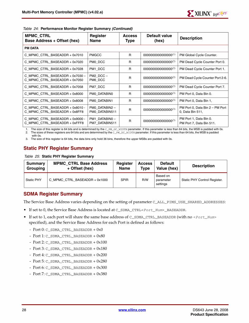
Table 24: Performance Monitor Register Summary
MPMC_CTRL Base Address + Offset (hex)
Register Name
Access Type
Default value (hex)
Description
PM CONTROL
C_MPMC_CTRL_BASEADDR + 0x7000 PMCTRL R/W 00000000 PM Control Register.
C_MPMC_CTRL_BASEADDR + 0x7004 PMCLR W 00000000 PM Clear Register.
C_MPMC_CTRL_BASEADDR + 0x7008 PMSTATUS R/TOW 00000000 PM Status Register.
27 www.xilinx.com DS643 June 28, 2008Product Specification
Multi-Port Memory Controller (MPMC) (v4.02.a)
Static PHY Register Summary
SDMA Register Summary
The Service Base Address varies depending on the setting of parameter C_ALL_PIMS_USE_SHARED_ADDRESSES:
• If set to 0, the Service Base Address is located at C_SDMA_CTRL<Port_Num>_BASEADDR.
• If set to 1, each port will share the same base address of C_SDMA_CTRL_BASEADDR (with no <Port_Num> specified), and the Service Base Address for each Port is defined as follows:
- Port 0: C_SDMA_CTRL_BASEADDR + 0x0
- Port 1: C_SDMA_CTRL_BASEADDR + 0x80
- Port 2: C_SDMA_CTRL_BASEADDR + 0x100
- Port 3: C_SDMA_CTRL_BASEADDR + 0x180
- Port 4: C_SDMA_CTRL_BASEADDR + 0x200
- Port 5: C_SDMA_CTRL_BASEADDR + 0x280
- Port 6: C_SDMA_CTRL_BASEADDR + 0x300
- Port 7: C_SDMA_CTRL_BASEADDR + 0x380
PM DATA
C_MPMC_CTRL_BASEADDR + 0x7010 PMGCC R 0000000000000000(1) PM Global Cycle Counter.
C_MPMC_CTRL_BASEADDR + 0x7020 PM0_DCC R 0000000000000000(2) PM Dead Cycle Counter Port 0.
C_MPMC_CTRL_BASEADDR + 0x7028 PM1_DCC R 0000000000000000(2) PM Dead Cycle Counter Port 1.
C_MPMC_CTRL_BASEADDR + 0x7030 – C_MPMC_CTRL_BASEADDR + 0x7050
PM2_DCC – PM6_DCC
R 0000000000000000(2) PM Dead Cycle Counter Port 2-6.
C_MPMC_CTRL_BASEADDR + 0x7058 PM7_DCC R 0000000000000000(2) PM Dead Cycle Counter Port 7.
C_MPMC_CTRL_BASEADDR + 0x8000 PM0_DATABIN0 R 0000000000000000(3) PM Port 0, Data Bin 0.
C_MPMC_CTRL_BASEADDR + 0x8008 PM0_DATABIN1 R 0000000000000000(3) PM Port 0, Data Bin 1,
C_MPMC_CTRL_BASEADDR + 0x8010 - C_MPMC_CTRL_BASEADDR + 0x8FF8
PM0_DATABIN2 – PM0_DATABIN511
R 0000000000000000(3) PM Port 0, Data Bin 2 – PM Port 0, Data Bin 511,
C_MPMC_CTRL_BASEADDR + 0x9000 - C_MPMC_CTRL_BASEADDR + 0xFFF8
PM1_DATABIN0 – PM7_DATABIN511
R 0000000000000000(3) PM Port 1, Data Bin 0.PM Port 7, Data Bin 511.
1. The size of this register is 64 bits and is determined by the C_PM_GC_WIDTH parameter. If this parameter is less than 64 bits, the MSB is padded with 0s.2. The sizes of these registers are 64 bits and are determined by the C_PM_DC_WIDTH parameter. If this parameter is less than 64 bits, the MSB is padded
with 0s.3. The size of this register is 64 bits, the data bins only hold 36 bins, therefore the upper MSBs are padded with 0s.
Table 25: Static PHY Register Summary
Summary Grouping
MPMC_CTRL Base Address + Offset (hex)
Register Name
Access Type
Default Value (hex)
Description
Static PHY C_MPMC_CTRL_BASEADDR + 0x1000 SPIR R/WBased on parameter settings
Static PHY Control Register.
Table 24: Performance Monitor Register Summary (Continued)
MPMC_CTRL Base Address + Offset (hex)
Register Name
Access Type
Default value (hex)
Description
28 www.xilinx.com DS643 June 28, 2008Product Specification

Multi-Port Memory Controller (MPMC) (v4.02.a)
The following table shows the SDMA registers and the PLB address offset form the Service Base Address assign-ment with the allowed access to that register.
Table 26: SDMA Registers
PLB Address Offset from Service Base Address
AssignmentRegister Name
Access Type
Default Value (hex)
Description
Transmit Registers
0x00 TX_NXTDESC_PTR R 00000000 TX Next Descriptor Pointer.
0x04 TX_CURBUF_ADDR R 00000000 TX Current Buffer Address.
0x08 TX_CURBUF_LENGTH R 00000000 TX Current Buffer Length.
0x0C TX_CURDESC_PTR R/W 00000000 TX Current Descriptor Pointer.
0x10 TX_TAILDESC_PTR R/W 00000000 TX Tail Descriptor Pointer.
0x14 TX_CHNL_CTRL R/W 00000000 TX Channel Control.
0x18 TX_IRQ_REG R/W 00FF0000 TX Interrupt Register.
0x1C TX_CHNL_STS R 00000000 TX Status Register.
Receive Registers
0x20 RX_NXTDESC_PTR R 00000000 RX Next Descriptor Pointer.
0x24 RX_CURBUF_ADDR R 00000000 RX Current Buffer Address.
0x28 RX_CURBUF_LENGTH R 00000000 RX Current Buffer Length.
0x2C RX_CURDESC_PTR R/W 00000000 RX Current Descriptor Pointer.
0x30 RX_TAILDESC_PTR R/W 00000000 RX Tail Descriptor Pointer.
0x34 RX_CHNL_CTRL R/W 00000000 RX Channel Control.
0x38 RX_IRQ_REG R/W 00FF0000 RX Interrupt Register.
0x3C RX_CHNL_STS R 00000000 RX Status Register.
Control Registers
0x40 DMA_CONTROL_REG R/W 0000001C DMA Control Register.
29 www.xilinx.com DS643 June 28, 2008Product Specification

Multi-Port Memory Controller (MPMC) (v4.02.a)
30
MPMC Use CasesYou can use MPMC to build different system use cases. Because of software variables, device bus trans-actions, memory latency, and speed; each system is capable of different size and data bandwidths. MPMC allows you to build systems quickly for different use cases, and then compare the size and the performance. There are many more use cases than can be shown; the use cases in this document can be used as an aide to understanding what types of trade-offs can be made when configuring MPMC. Each application is different, and no use case is ideal for all applications.
The following subsections provide examples of these available system use cases:
• Standard PowerPC 405 CoreConnect
• Single-Processor MicroBlaze
• Dual-Processor PowerPC 405
Standard PowerPC 405 CoreConnect Use Case
An MPMC module fits easily into existing PowerPC 405 CoreConnect-based systems as a single-port memory controller as shown in the following figure. This is particularly useful as a starting point to port an existing design into an MPMC use case that allows for improved performance.
Figure Top x-ref 1
Figure 1: Standard PowerPC CoreConnect Use Case
PLBPIM
PPC405
DeviceDevice
Memory
PLBARB
DS643_01_082107
MPMCDPLB0
IPLB0
www.xilinx.com DS643 June 28, 2008Product Specification

Multi-Port Memory Controller (MPMC) (v4.02.a)
DS643 JuneProduct Sp
Single Processor MicroBlaze Use Case
The following figure shows an example of a common MicroBlaze system layout. The MPMC module provides direct memory access to the processor IXCL and DXCL interfaces.
A standard PLB port is defined for use with PLB devices. The MicroBlaze processor can be connected directly to the PLB bus attached to the PLB PIM also.
Figure Top x-ref 2
Figure 2: Single Processor MicroBlaze Use Case
PLBPIM
XCLPIM
XCLPIM
MicroBlazeMemory
Device
Device
PLBARB
DS643_02_082207
MPMC
IPLB DPLB
IXCL
DXCL
28, 2008 www.xilinx.com 31ecification

Multi-Port Memory Controller (MPMC) (v4.02.a)
32
Dual Processor PowerPC 405 Use Case
This figure shows an example of two PowerPC 405 processors connected directly to an MPMC module.
On the first PowerPC 405 processor:
• The IPLB1 and DPLB1 ports of the first PowerPC 405 are connected to the first two MPMC PLB PIMs. These are point to point connections for improved performance. Additionally, the PLB PIMs are designated as IPLB and DPLB PIMs to allow for performance optimizations inside of the PIM.
• The IPLB0 and DPLB0 ports of the first PowerPC 405 are connected to the PLB Bus attached to the third PLB PIM. Also attached to the PLB Bus are block RAM memory, which can be used to boot code and other PLB devices necessary to a particular application.
On the second PowerPC 405 processor:
• The IPLB1 and DPLB1 ports of the second PowerPC 405 processor are connected directly to the fourth and fifth PLB PIMs.
• The IPLB0 and DPLB0 ports of the second PowerPC 405 are connected to the PLB bus attached to the sixth PLB PIM. Also on this PLB bus are the block RAM memory, which can be used to boot code and other “low-bandwidth” PLB devices.
• On the seventh PLB PIM is a “high bandwidth” PLB device. This device has a direct connection to MPMC to improve performance. The configuration PLB port of this high bandwidth device is connected to the sixth PLB PIM to allow configuration from the second PowerPC 405 processor.
Figure Top x-ref 3
Figure 3: Dual Processor PowerPC Use Case
PLB
PLB
PIM
PLBPIM
PLBPIM
PLBPIM
PLBPIM
PIM
PLBPIM
Memory
Device
Device
PLBARB DS643_03_082007
BRAM
IPLB0 DPLB0
DPLB1
IPLB1
PPC405
Device
Device
PLBARB
BRAM
IPLB0 DPLB0
DPLB1
IPLB1
PPC405
MPMC
(IPLB)
(DPLB)
(IPLB)
(DPLB)
low bandwidth
low bandwidthDevice
high bandwidthConfigPLBPort
MasterPLBPort
www.xilinx.com DS643 June 28, 2008Product Specification

Multi-Port Memory Controller (MPMC) (v4.02.a)
DS643 JuneProduct Sp
Memory Controller ArchitectureThe MPMC architecture comprises the following components:
• "Address Path"
• "Data Path"
• "Control Path / Arbiter"
• "Configurable Physical Interface"
• "IDELAY Controller" (Only available with specific PHY Interfaces)
• "Clock and Reset Logic"
• "Transaction Ordering and Memory Coherency"
In addition, the MPMC provides features which are described in separate sections of this document, and are included within the architectural diagram to provide a comprehensive overview. Throughout this document, the term “word” signifies a 32-bit word.
• "Control and Status Registers" (only available when using optional features.) The descriptions of these registers are provided in the Design Parameters section under "Control and Status Registers" page 27.
• "Personality Interface Modules" page 62, which contains:
- "Xilinx CacheLink"
- "Soft Direct Memory Access Controller for LocalLink Interfaces"
- "Processor Local Bus Version 4.6 PIM"
- "PowerPC 440 Memory Controller PIM"
- "Video Frame Buffer Controller PIM"
- "Native Port Interface PIM"
• "Error Correction Code" page 128 (optional)
• "Performance Monitoring" page 138 support (optional)
The following figure is a block diagram of the MPMC architecture. The following subsections describe the MPMC architectural features
28, 2008 www.xilinx.com 33ecification

Multi-Port Memory Controller (MPMC) (v4.02.a)
Figure 4: MPMC Architecture Block Diagram
DS643_04_082207
PIM0(configurable) Data
Path
ControlPath/
Arbiter
AddressPath
Control Registers
NPI
PerformanceMonitor
PIM1(configurable)
NPI
PerformanceMonitor
PIM2(configurable)
NPI
PerformanceMonitor
PIM3(configurable)
NPI
PerformanceMonitor
PIM4(configurable)
NPI
PerformanceMonitor
PIM5(configurable)
NPI
PerformanceMonitor
PIM6(configurable)
Connections toPIMs and/orPerformanceMonitors
PLBInterface
NPI
PerformanceMonitor
PIM7(configurable)
NPI
PerformanceMonitor
Po
rt R
ou
ting
Lo
gic
EC
C S
up
po
rt
Me
mo
ry(S
DR
AM
, D
DR
, o
r D
DR
2)
PH
Y(c
on
figu
rabl
e)
ResetLogic IDELAY
Controller
MPMC
34 www.xilinx.com DS643 June 28, 2008Product Specification

Multi-Port Memory Controller (MPMC) (v4.02.a)
DS643 JuneProduct Sp
Address Path
The address path allows each PIM to have independent access. Each PIM supports 32-bit addresses. This allows at least one 32-bit address from each PIM to be acknowledged simultaneously. Then, the control path determines the order that the addresses go to memory. Refer to "Transaction Ordering and Memory Coherency" page 61 for more details.
The address path information includes the following topics:
• "Base/High/Offset Parameters"
• "Address Encoding"
• "Address Path Pipeline"
• "Address Alignment by Read and Write Request"
Base/High/Offset Parameters
Each PIM has PIM-specific Base/High/Offset address parameters. Refer to the documentation of the PIM you are using for correct address information. The MPMC parameters are listed in "Design Param-eters" page 2. The Base/High/Offset parameters are defined as a 32-bit value of C_<PIM_Type>_[BASEADDR|HIGHADDR|OFFSET]. The value set in the C_ALL_PIMS_SHARE_ADDRESSES parameter determines if all ports have a common base and high address or if each port has independently-configured memory address ranges. If you want to imple-ment a shadow/aliased memory you need to double the amount of addressable memory. This can be done by increasing the C_<PIM_Type>_HIGHADDR by an amount that will double the address range.
Address Encoding
MPMC does not perform address range validation, and MPMC will respond to all addresses, so it is the responsibility of the PIM to ensure that valid addresses are being passed across the NPI interface. The address path is responsible for translating the address into an encoded address that adheres to SDRAM, DDR, or DDR2 memory specifications.
The following memory parameters are used to encode the address:
• C_MEM_DATA_WIDTH
• C_MEM_PART_NUM_COL_BITS
• C_MEM_PART_NUM_ROW_BITS
• C_MEM_PART_NUM_BANK_BITS
• C_MEM_NUM_RANKS
• C_MEM_NUM_DIMMS
The memory address offsets are as follows:
• col_addr_startbit = log2(C_MEM_DATA_WIDTH/8)
• row_addr_startbit = col_addr_startbit + C_MEM_PART_NUM_COL_BITS
• bank_addr_startbit = row_addr_startbit + C_MEM_PART_NUM_ROW_BITS
• rank_addr_startbit = bank_addr_startbit + C_MEM_PART_NUM_BANK_BITS
• dimm_addr_startbit = rank_addr_startbit + C_MEM_NUM_RANKS
• total_addr_startbit = dimm_addr_startbit + C_MEM_NUM_DIMMS
28, 2008 www.xilinx.com 35ecification

Multi-Port Memory Controller (MPMC) (v4.02.a)
36
The following table shows the address column, row, bank, rank, DIMM, and total memory address.
You can set the base and high addresses of your custom PIM to cover this address space. Standard PIMs (such as PLB and XCL PIMs) have address range and offset parameters to handle how addresses are mapped from the bus interface to the physical memory.
Address Path Pipeline
The address path pipeline is controlled by C_PIM<Port_Num>_ADDRACK_PIPELINE, a per-port param-eter which, when set in the IP Configuration interface, allows the NPI address acknowledge signal to be registered. Enable this parameter to achieve better timing, but expect one extra cycle of latency on the assertion of address acknowledge. Refer to "IP Configuration Graphical User Interface" page 145 for more information on setting per-port parameters.
Address Alignment by Read and Write Request
When requesting a transfer, the parameter, PIM<Port_Num>_Addr, has alignment restrictions on Reads and Writes. The following subsections list the alignment restrictions by Read and Write request.
Read Requests
Addresses corresponding to a Read request must be aligned as follows:
• Word transfers (32-bit NPI only) are 4-byte aligned
• Double-word transfers (64-bit NPI only) are 8-byte aligned
• 4-word, cacheline transfers (32-bit NPI only) are 4-byte aligned
• 4-word, cacheline transfers (64-bit NPI only) are 8-byte aligned
• 8-word, cacheline transfers (32-bit NPI only) are 4-byte aligned
• 8-word, cacheline transfers (64-bit NPI only) are 8-byte aligned
• 16-word, burst transfers are 64-byte aligned
• 32-word, burst transfers are 128-byte aligned
• 64-word, burst transfers (64-bit NPI only when using SRL FIFOs, see the "Data Path" page 37) are 256-byte aligned
Table 27: Address Type and Corresponding Parameter
Memory Address Type Corresponds to:
Column PIM<Port_Num>_Addr[row_addr_startbit: col_addr_startbit]
Row PIM<Port_Num>_Addr[bank_addr_startbit-1:row_addr_startbit]
Bank PIM<Port_Num>_Addr[rank_addr_startbit-1:bank_addr_startbit]
Rank PIM<Port_Num>_Addr[dimm_addr_startbit-1:rank_addr_startbit]
DIMM PIM<Port_Num>_Addr[total_addr_startbit-1:dimm_addr_startbit]
Total memory space PIM<Port_Num>_Addr[total_addr_startbit-1:0]
www.xilinx.com DS643 June 28, 2008Product Specification

Multi-Port Memory Controller (MPMC) (v4.02.a)
DS643 JuneProduct Sp
Write Requests
Addresses corresponding to a Write request must be aligned to the size of the requested transfer as fol-lows:
• Word transfers (32-bit NPI only) are 4-byte aligned
• Double-word transfers (64-bit NPI only) are 8-byte aligned
• 4-word cache-line transfers are 16-byte aligned
• 8-word cache-line transfers are 32-byte aligned
• 16-word burst transfers are 64-byte aligned
• 32-word burst transfers are 128-byte aligned
• 64-word burst transfers (64-bit NPI only when using SRL FIFOs, see the "Data Path" page 37) are 256-byte aligned
Data Path
The MPMC data path comprises the following:
• "Supported Data Widths"
• "FIFO Types"
• "Read Word Address"
• "Data Path Pipelines"
Supported Data Widths
MPMC supports NPI data widths of 32 and 64 bits. In the discussion of data widths, “32-bit NPI” refers to an NPI data width of 32-bits, “64-bit NPI” refers to an NPI data width of 64-bits, and “NPI” refers to either 32- or 64-bit data widths.
The data path also supports SDRAM, DDR, and DDR2 memories that have total physical data widths of 8, 16, 32, and 64 bits.
FIFO Types
In MPMC, you can select either block RAM (BRAM) or 16-bit Shift Register Lookup (SRL) table FIFOs. Generally, a block RAM FIFO gives the best performance because the timing is better and the FIFO depth is larger and does not create stalls in the data path due to a full FIFO condition. The write block RAM FIFO does not assert the PIM<Port_Num>_WrFIFO_AlmostFull which can also simplify the design of PIMs because the PIM does not need to dynamically monitor the almost full flag. The PIM is therefore required to ensure that a block RAM FIFO will never reach a write FIFO full state. The block RAM FIFO also provides better timing than an SRL FIFO which may allow for a higher Fmax. This is especially true for Spartan-3 where the timing on the SRL primitive is significantly worse than the tim-ing on block RAM primitive timing. In some cases, however, an SRL FIFO can improve system timing versus a block RAM FIFO when the MPMC has a large number of ports and routing to the all the block RAMs results in excessive net delays.
Some configurations of MPMC might require more block RAMs than are available on a particular device, in which case the SRL FIFOs can be used. Additionally particular applications or system con-figurations can use a significant number of block RAMs, leaving few resources for MPMC.
28, 2008 www.xilinx.com 37ecification

Multi-Port Memory Controller (MPMC) (v4.02.a)
38
The number of block RAM or SRL resources consumed by the FIFOs depends on:
• Number of ports and whether a particular port has read FIFOs, write FIFOs, or both
• NPI data width and memory data width
See the "Resource (block RAM) Utilization" page 151 for more information about block RAM utilization in MPMC. This section also explains how many LUTs are used when a SRL FIFO is selected.
Read Word Address
When Read data for a cacheline request is returned, it might not be returned target-word first. Read data is returned sequentially, but it could be returned where the requested target word appears later in the sequence than desired due to memory access optimizations and the allowance of back-to-back read requests. You must monitor the PIM<Port_Num>_RdFIFO_RdWdAddr output value to determine which word is being returned first.
Data Path Pipelines
The following table outlines the pipeline stages in the MPMC data path; which is set using the MPMC interface. See the "IP Configuration Graphical User Interface" page 145 for more information about set-ting the pipeline. Adding pipeline stages improves timing but also increases latency.
Table 28: MPMC Data Path Pipelines
Pipeline Stage Description
Write Data Path input Registers the write FIFO inputs (push, FIFO address, data, byte enables).
Write Data Path outputRegisters the write FIFO outputs (data, byte enables). All ports must have the same setting.
Write Data Path timing management
There is a multiplexer (MUX) that selects which write FIFO the PHY is currently using. This pipeline stage adds a register after that MUX
Read Data Path inputRegisters the read FIFO inputs (push, FIFO address, data). All ports must have the same setting.
Read Data Path output Registers the read FIFO outputs (data, read word address).
Read Data Path fanout
The read data going from the PHY to the data path is routed to the read FIFO for each port. If the FIFOs are spaced far apart (which is likely when using block RAM FIFOs), the routing delays can be largeSetting the fanout has the following effect:
• 0 = No register is instantiated.
• 1 = Read data is forwarded from the PHY for up to eight sets of registers. The outputs of the registers are then forwarded on to a maximum of one read FIFO.
• 2 = Read data is forwarded from the PHY to up to four sets of registers. The outputs of the registers are the forwarded on to a maximum of two read FIFOs.1.
• 4 = Read data is forwarded from the PHY to two sets of registers. The outputs of the registers are the forwarded on to a maximum of four read FIFOs.1
• 8 = Read data is forwarded from the PHY to a single register, then for-warded on to each of the read FIFOs.
Note:1. Values of 3, 5, 6, 7 are invalid.
www.xilinx.com DS643 June 28, 2008Product Specification

Multi-Port Memory Controller (MPMC) (v4.02.a)
DS643 JuneProduct Sp
Control Path / Arbiter
The MPMC control path is configured for optimal memory bandwidth given a particular memory. It can be configured to support different physical (PHY) interfaces also. The following subsections describe the Control Path/Arbiter:
• "Transfer Types"
• "Arbitration Algorithms"
• "Arbiter Pipeline"
• "Control Path/Arbiter block RAM Utilization"
Transfer Types
The control path supports the following transfer types:
• Word reads and writes (32-bit NPI only).
• Double-word reads and writes (64-bit NPI only).
• 4-word, cacheline reads and writes.
• 8-word, cacheline reads and writes.
• 16-word, burst reads and writes.
• 32-word, burst reads and writes.
• 64-word, burst reads and writes (64-bit NPI only when using SRL FIFOs).
Arbitration Algorithms
The MPMC Arbiter supports the following arbitration algorithms:
• Round Robin
• Fixed
• Custom
For more information on how to configure the arbiter, see the "Arbitration" information in the "IP Con-figuration Graphical User Interface" page 145.
Arbiter Pipeline
An optional pipeline is allowed in the arbitration logic. To achieve best timing, enable this pipeline using the IP Configuration interface. Enabling the arbiter pipeline could also increase latency. See the "Arbitration" information in the "IP Configuration Graphical User Interface" page 145 for more information.
Control Path/Arbiter block RAM Utilization
The MPMC control logic is designed around a block RAM-based state machine; therefore, the control logic always consumes one block RAM.
The arbiter uses one block RAM when a custom arbitration algorithm is used. With Fixed or Round Robin arbitration, or when C_NUM_PORT is set to 1, no additional block RAM is needed.
28, 2008 www.xilinx.com 39ecification

Multi-Port Memory Controller (MPMC) (v4.02.a)
40
Configurable Physical Interface
The MPMC Physical Interface (PHY) is the interface situated between memory and the MPMC address path, control path, and data path. The PHY interface can be configured to support SDRAM, DDR SDRAM, and DDR2 SDRAM memories across Virtex-II Pro, Virtex-4, Virtex-5, and Spartan-3 (3/3A/3E/3AN/3ADSP) platforms. Mobile DDR memories are not currently supported by any PHY interface.
These sections describe the following topics:
• "Memory Interface Generator Based PHY Interface"
• "Static PHY Interface"
• "SDRAM PHY Interface"
• "Connecting Memory to the PHY Interface"
The PHY interface options are:
• "Memory Interface Generator Based PHY Interface": (MIG)-based PHY interface is a DDR/DDR2 physical memory interface core/reference design technology used by MPMC. See "Reference Documents" page 163 for links to more information about MIG. This is the recommended PHY interface. Using MIG-based PHY requires that you follow the MIG FPGA pinout and board layout guidelines. You must use the MIG tool to generate pinout, placement, and timing constraints (UCF file constraints) for MPMC designs. MPMC uses the Static PHY instead of the MIG-based PHY for Virtex-II Pro. Mobile DDR and Low Power DDR are not supported by MPMC.
• "Static PHY Interface": You can use the Static PHY when MIG pinout and layout guidelines were not followed. The Static PHY is currently available for DDR and DDR2 memories only. The Static PHY must be used with Virtex-II Pro. Mobile DDR and Low Power DDR are not supported by MPMC.
• "SDRAM PHY Interface": SDRAM PHY is the interface between the Single Data Rate Access Memory (SDRAM) and the MPMC control path, address path, and data path. The SDRAM PHY interface supports Virtex-4, Virtex-5, and Spartan-(3/3E/3A/3AN/3ADSP) platforms. MPMC can read and write to Mobile SDRAM devices, but MPMC does not make use of the low power features of Mobile SDRAM, such as deep power down or partial-array refresh.
The following table summarizes the available PHY interfaces available for each FPGA device family and memory combination.
Table 29: PHY Layer by Xilinx FPGA Family and Memory Type
FPGA Family Memory Type
DDR2 DDR SDRAM
Virtex-5MIG-Based Virtex-5 DDR2 PHY (1)
Static PHYMIG-Based Virtex-5 DDR PHY (1)
Static PHYSDRAM PHY (1)
Virtex-4MIG-Based Virtex-4 DDR2 PHY (1)
Static PHYMIG-Based Virtex-4 DDR PHY (1)
Static PHYSDRAM PHY (1)
www.xilinx.com DS643 June 28, 2008Product Specification

Multi-Port Memory Controller (MPMC) (v4.02.a)
DS643 JuneProduct Sp
Memory Interface Generator Based PHY Interface
The Memory Interface Generator (MIG)-based PHY interface contains input and output flip-flops, read data delay logic, data capture logic, and memory initialization logic.
The read data delay logic uses IDELAYs for Virtex-4 and Virtex-5 families, and Look-Up Table (LUT) delays for Spartan-3 platforms. The delay logic is used to align the middle of the valid read data to the MPMC_Clk0 clock edge. This is necessary to accommodate for variations in trace delays on different boards. The delay elements change the time that the read data arrives at the FPGA to align it to the main clock.
In Virtex-4 and Virtex-5 families, this alignment is done as part of the memory initialization logic. At the end of the initialization/configuration sequence, the PHY issues dummy write and read com-mands. The delay logic then determines the edges of the input data and shifts the input data to allow MPMC_Clk0 to properly capture the data. To ensure a robust interface, you must match the trace lengths for the data signals to the corresponding data strobe signal and ensure that the proper FPGA I/O pin selections are made as described in the MIG User Guide. “Reference Documents,” page 163 has a link to the MIG web page that contains the user guide.
In DDR and DDR2 cases, the data capture logic then takes the DDR read data and turns it into Single Data Rate (SDR) data. In SDRAM cases, the data is already available as SDR data. The PHY then pushes the data into the data path FIFOs, making it available to the NPI.
For more information on the use of IDELAY in DDR and DDR2 applications see the “Memory Interfaces Data Capture Using Direct Clocking Technique” document. The “Reference Documents,” page 163 con-tains a link to this document.
For more information about the MIG physical interface design, register and download the MIG design. The “Reference Documents,” page 163 contains a link to the Xilinx Memory webpage where the MIG design is located.
Virtex-II Pro Static PHY(1) Static PHY(1) SDRAM PHY (1)
Spartan-3Spartan-3ESpartan-3ASpartan-3ANSpartan-3ADSP
MIG-Based Spartan-3 DDR2 PHY (1)
Static PHY
MIG-Based Spartan-3 DDR PHY(1)
Static PHYSDRAM PHY (1)
1. Note: Default selection.
Table 29: PHY Layer by Xilinx FPGA Family and Memory Type (Continued)
FPGA Family Memory Type
28, 2008 www.xilinx.com 41ecification

Multi-Port Memory Controller (MPMC) (v4.02.a)
42
MIG-Based PHY Design Considerations
The following are design considerations for using the MIG-based PHY interface:
• This version of MPMC should be used with MIG v2.1. Older or newer versions of MIG might not produce a User Constraint File (UCF) compatible with this version of MPMC. Scripts are provided to migrate MPMCv3 designs based on MIG v1.73 to MPMCv4. See “Migrating an MPMCv3 Design to MPMCv4,” page 45 for more information.
• Virtex-5 DDR2 boards should be designed to support differential DQS.
• It is required and extremely important to ensure that the layout and pinout of any other boards to be used with MPMC follow the design requirements of MIG v2.1. Failure to follow MIG design rules and all applicable MIG UCF constraints could result in an inoperable MPMC. A MIG UCF conversion script is described in the following section.
• If using ECC, ensure that the board supports a full 8 bit wide data byte lane for the ECC check bits. In previous versions of MPMC, only 4 physical bits were used for ECC, but this and all future versions of MPMC require the full byte lane to be present to accommodate the PHY data calibration algorithm.
• During memory initialization (following reset), the Virtex-4 and Virtex-5 DDR and DDR2 MIG-based PHY writes to the top locations in memory to set up the write training pattern. This can affect memory address between {C_MPMC_HIGHADDR - 0xFF} and C_MPMC_HIGHADDR; therefore, after any reset, these locations in memory are overwritten. Software code should not be stored in the top 0x100 address locations of memory. If you are using shadow memory, review the "Address Encoding" page 35 to determine which address locations will be overwritten.
• In multi-rank systems, the MIG PHY will only calibrate its data capture timing to one of the ranks on one of the DIMMs. Differences in timing, process variation across memory devices, or bus loading affects across ranks will reduce timing margin and can affect the frequency range of operation.
Note: Multi-rank/multi-DIMM systems are not tested or characterized by MIG. Care must be taken to ensure that the maximum skew and signal integrity is controlled across ranks. The use of Multi-Rank designs is strongly discouraged. The use of multi-DIMM designs is currently unsupported.
www.xilinx.com DS643 June 28, 2008Product Specification

Multi-Port Memory Controller (MPMC) (v4.02.a)
DS643 JuneProduct Sp
MIG-based PHY Design and Implementation Considerations for Spartan-3 and Virtex-5 DDR2
MPMC uses the Spartan-3 PHY from MIGv2.1 to implement the physical level interface for Spartan-3 (3/3A/3AN/3E/3ADSP) platforms. The MIG Spartan-3 and Virtex-5 DDR2 PHYs use very specific UCF constraints to constrain the pinout and placement of internal elements in the fabric. These constraints are specific to an individual Spartan-3 or Virtex-5 FPGA device and are not necessarily por-table across devices (even if the different devices are in the same package).
MIG also has guidelines for the board layout of the memory interface so that the PHY functions prop-erly. It is extremely important that any user boards be designed in compliance with the MIG v2.1 pinout constraints and layout guidelines for Spartan-3 and other MIG PHY families. MIG provides a Graphical User Interface (GUI) in the Coregen tool that guides you through the process of generating the pinout and UCF constraints for their design.
Note: MPMC does not support the use of top/bottom memory interface banks for the Spartan-3 FPGA family (C_FAMILY parameter = “spartan3”). Do not choose top or bottom banks for the memory interface in the MIG v2.1 tool. You must choose the left or right side banks for the memory interface pinout.
For Spartan-3 (3/3A/3AN/3E/3ADSP) designs, ensure that the system clock input pin is correctly specified to the MIG v2.1 tool. This will cause the MIG tool to place a “cal_ctl” area group near the BUFG corresponding to the location of the system clock input pin. Make sure that in the final design the “cal_ctl” area group corresponds to the location near the BUFG that drives MPMC_Clk0.
Answer Records, Application Notes, and the MIG User Guide provide important information about the Spartan-3 PHY, the MIG UCF constraints, and board layout guidelines. These resources will help to debug and bring up MPMC designs using the MIG PHY:
• The Xilinx memory page contains the MIG User Guide and other relevant content.
• Answer Records contain useful design, debug, and implementation content.
• Application Notes, XAPP768C and XAPP454, are specific to data write and data read capture techniques and DDR2 SDRAM memory interfaces for Spartan-3 FPGAs.
The “Reference Documents,” page 163 contains links to these resources. The UCF generated by the MIG tool cannot be used directly in MPMC designs because the path names of internal elements differ.
28, 2008 www.xilinx.com 43ecification

Multi-Port Memory Controller (MPMC) (v4.02.a)
44
Converting MIGv2.1 UCF to MPMCv.4 UCF
A script is provided at:<EDK Install Dir>/hw/XilinxProcessorIPLib/pcores/mpmc_v4_01_a/data/convert_ucf.pl to assist with the process of converting a MIG v2.1 UCF into an MPMCv4.01.a UCF.
After running the MIG v2.1 tool to generate a Verilog MIG design, take the UCF file from the /mig_21/user_design/par directory and execute this script in a shell where ISE™ and EDK tools are in the path environment:
xilperl <EDK Install Dir>/hw/XilinxProcessorIPLib/pcores/mpmc_v4_01_a/data/convert_ucf.pl <MIG UCF> <USER UCF>
The <USER UCF> file has UCF path names modified to match MPMC path names. You must add the contents of the <USER UCF> file manually into the <EDK_Project_Directory>/data/system.ucf file.
This script is provided to assist with the process of translating the UCF but it does not necessarily gen-erate a complete working UCF to use with MPMC. You must still verify the output of the script and you might need to adjust it to fit a particular design. The script does not completely translate the names of clock, reset, or memory I/O signals to match the top level port names in the EDK design. You must translate these signal names to match your design.
If you are using the Virtex5 DDR2 PHY, you must also open the MIG file located at /mig_21/user_design/rtl/ddr2_sdram.v. For example, the HDL lines:
PARAMETER C_MEM_DQS_IO_COL = 0b000000000000000000PARAMETER C_MEM_DQ_IO_MS =0b10101001111000110010101011110100100100010011010010101110111100011101001
would be added to the MPMC MHS instance as:
PARAMETER C_MEM_DQS_IO_COL = 0b000000000000000000PARAMETER C_MEM_DQ_IO_MS = 0b10101001111000110010101011110100100100010011010010101110111100011101001
The MPMC GUI > Memory Interface > MIG Settings uses the same value format as the above MHS snippet. Search for the parameters DQS_IO_COL and DQ_IO_MS, note the values for these parameters, open the MPMC GUI >Memory Interface >MIG Settings, and assign these values to C_MEM_DQS_IO_COL and C_MEM_DQ_IO_MS.
www.xilinx.com DS643 June 28, 2008Product Specification

Multi-Port Memory Controller (MPMC) (v4.02.a)
DS643 JuneProduct Sp
Migrating an MPMCv3 Design to MPMCv4
Two additional scripts are provided to revise (rev-up) an MPMC v3.00.a or v3.00.b design that uses a MIG v1.73 PHY to an MPMC v4.01.a design that uses a MIG v2.1 PHY. If you are using the Virtex-4 DDR or DDR2 MIG PHY or the Virtex-5 DDR PHY, no rev-up is required.
• To revise a Spartan-3 (3/3A/3AN/3E/3ADSP) DDR or DDR2 design, execute the following commands in a shell where ISE tools are in the path:
cd <EDK Install Dir>/hw/XilinxProcessorIPLib/pcores/mpmc_v4_01_a/data
xilperl revup_s3_ucf.pl <MPMC v3 UCF> <USER UCF>
where:
- <EDK Install Dir> is the directory in which the EDK is installed.
- <MPMC v3 UCF> is the name of your UCF file from your mpmc_v3_00_a or mpmc_v3_00_b project.
- <USER UCF> is the UCF file to be used in your mpmc_v4_01_a project.
To revise a Virtex-5 DDR2 design, execute the following commands in a shell where ISE and EDK tools are in the path:
cd <EDK Install Dir>/hw/XilinxProcessorIPLib/pcores/mpmc_v4_01_a/data
xilperl revup_v5_ucf.pl <MPMC v3 UCF> <PART NUMBER> <DQ PIN NAME> <DQSn PIN NAME> <USER UCF> <MHS SNIPPET>
where:
- <MPMC v3 UCF> is the name of the UCF file from your mpmc_v3_00_a or mpmc_v3_00_b project.
- <PART NUMBER> is the FPGA part you are targeting; for example xc5vlx50ff676.
- <DQ PIN NAME> is the base name of the DQ pins in your UCF file, without bus indices.
- <DQSn PIN NAME> is the base name of the DQSn pins in your UCF file, without bus indices.
- <USER UCF> is the output UCF file that should be used in your mpmc_v4_01_a project.
- <MHS SNIPPET> is the name of an output text file that contains the new MPMC parameter settings.
The new MHS values can be copied into the configuration portion of the MPMC GUI >Memory Inter-face >MIG Settings, and transferring these values into the corresponding C_MEM_DQS_IO_COL and C_MEM_DQ_IO_MS parameters in the interface.
Also, you can cut and paste the snippet directly into the MPMC section of the MHS file.
For example:
xilperl C:/Xilinx/EDK/hw/XilinxProcessorIPLib/pcores/mpmc_v4_01_a/data/revup_v5_ucf.pl C:/myproject/etc/system.ucf xc5vlx330tff1738
fpga_0_DDR2_SDRAM_32Mx64_DDR2_DQ fpga_0_DDR2_SDRAM_32Mx64_DDR2_DQS system_new.ucf system_new.mhs
For Virtex-5 DDR2 MIG PHY designs, a new PORT called MPMC_Clk0_DIV2 must be connected to a clock that is 1/2 the frequency of and synchronous to MPMC_Clk0. This PORT specification is a new requirement for MPMCv4. Migrating a design with multiple MPMCs requires multiple invocations of the revup_v5_ucf.pl script.
28, 2008 www.xilinx.com 45ecification

Multi-Port Memory Controller (MPMC) (v4.02.a)
46
Static PHY Interface
The Static PHY interface available in MPMC is based on DCM phase adjustment. This PHY can be used in cases when a MIG-based PHY is not available or cannot be used. The MPMC Static PHY interface is an alternative to the Memory Interface Generator (MIG)-based PHY interface. The Static PHY uses DCM-based fine phase adjustments to generate a read data capture clock instead of using IDELAYs or LUT-based delays to shift the input read data.
Note: Xilinx recommends that you design for, and use, a MIG-based PHY whenever possible for best results. MIG-based PHY interfaces offer greater timing margin, are more robust, and use fewer global clock buffer resources; the Static PHY is available when MIG-based PHY is not an option. As an example, the Static PHY might be used when a legacy board that was designed for a different memory controller and does not use a MIG-compatible pinout. All new designs should target the use of the MIG-based PHY.
Static PHY contains the following topics:
• "Static PHY Implementation"
• "Static PHY Implementation Considerations"
• "Static PHY Interface Register"
Static PHY Implementation
The following figure shows the Static PHY interface read logic:
Figure Top x-ref 4
Figure 5: Static PHY Interface Read Logic
MPMC_Clk_Mem MPMC_Clk0
RDDATA_CLK_SEL
MPMC_Clk0
RDDATA_SWAP_RISE
data toread FIFOs
read enable from control path
read enable to data path
DS643_05_071307
DDR to SDRdata conversion
Select positive ornegative clock edge
for re-alignment
Compensate if DDRdata shifted by 1/2
clock cycle
MPMC_Clk0
RDEN_DELAY
SRLDelay
Element
www.xilinx.com DS643 June 28, 2008Product Specification

Multi-Port Memory Controller (MPMC) (v4.02.a)
DS643 JuneProduct Sp
The Static PHY processes the read data as follows:
1. First, the Static PHY registers the read data on a clock (MPMC_Clk_Mem), which is typically provided by an additional Digital Clock Manager (DCM). This clock is, typically, a phase-shifted version of MPMC_Clk0. The phase is set to maximize timing margin on the captured read data. The read data goes through input flip-flops and is converted to Single Data Rate (SDR) data that is aligned on the rising edge of MPMC_Clk_Mem.
2. The data is then re-registered into the main MPMC clock domain (MPMC_Clk0).
Depending on the phase relationship between MPMC_Clk_Mem and MPMC_Clk0, you might need to first re-register the data on the negedge of MPMC_Clk0 before being registered on the positive edge. The selection using positive or negative edges of MPMC_Clk0 depends on the relative phase of MPMC_Clk_Mem:
- If MPMC_Clk_Mem is 0 to +180 degrees ahead of MPMC_Clk0, register the data on the positive edge of MPMC_0_Clk0.
- If MPMC_Clk_Mem is 0 to -180 degrees behind MPMC_Clk0, register the data on the negative edge of MPMC_Clk0.
The C_STATIC_PHY_RDDATA_CLK_SEL parameter sets the default value for this selection. You can change this value using the software interface at a later time, if necessary.
3. Next, data from the Static PHY passes through a selector to determine how the DDR data from memory is aligned with respect to positive and negative edges of MPMC_Clk_Mem.
Depending on board layout and clock frequency, it is possible that the data that is registered on the posedge of MPMC_Clk_Mem should be registered on the negedge of MPMC_Clk_Mem.
This clock phase relationship makes the SDR data appear misaligned with respect to the pairs of DDR data from memory. In this case, half of the data appears on the first posedge of MPMC_0_Clk0, and half of the data appears on the second posedge of MPMC_Clk0.
A multiplexor (MUX) lets you correct for the misalignment by selecting how the DDR data should be arranged into Single Data Rate (SDR) data. The default value of the MUX is controlled by the C_STATIC_PHY_RDDATA_SWAP_RISE parameter. You can change this value using the software interface at a later time, if required.
4. The last part of the Static PHY consists of a shift register that can adjust the delay of the read enable signal to the data path (which causes read data to be pushed into the read FIFO).
Depending on the parameter settings, clock frequency, and board layout, the read data to the data path might appear on a different clock cycle relative to the read enable signal from the control path.
The control path sends a read enable to the PHY at the same time that it sends the read command to the PHY. The PHY then must delay this signal for a certain number of cycles to make the read FIFO push signal valid at the same time as the data coming out of the Static PHY.
The C_STATIC_PHY_RDEN_DELAY parameter sets the default value for this delay. You can change this value using the software interface at a later time, if required.
If this parameter is set incorrectly, and a read is performed, it is possible that the read data will be pushed into a different FIFO than where the data was intended. This typically will occur only if the read was not issued on port 0. If the data is pushed into the wrong FIFO, the result can be identified by a processor hang that can be recovered from by resetting the system only. The correct setting for this parameter depends on MPMC pipeline configurations, clock frequency, and board layout, but typically this parameter is set to 5, 6, or 7.
28, 2008 www.xilinx.com 47ecification

Multi-Port Memory Controller (MPMC) (v4.02.a)
48
Additionally, if you are generating the MPMC_Clk_Mem with a DCM that is enabled to use variable phase shift, the DCR interface provides an easy way to control the PSEN and PSINCDEC ports of the DCM. MPMC provides a control port that can be connected to a DCM control port. This allows you to control the DCM phase adjust via the MPMC control registers. See the “Static PHY Interface Register,” page 49 for more details.
Static PHY Implementation Considerations
The important implementation considerations when using the Static PHY are:
• "Control Register Values"
• "Timing Constraints"
• "DCM Phase Adjust Port"
• "Matching Delay Traces"
The following subsections detail the implementation considerations.
Control Register Values
If you already know the control register values needed for the Static PHY to work with your board and this value is stable, you can choose to fix these values so that the PHY operates correctly upon power-on. You can do this by setting the DCM phase adjust and parameters values for C_STATIC_PHY_RDDATA_CLK_SEL, C_STATIC_PHY_RDDATA_SWAP_RISE, and C_STATIC_PHY_RDEN_DELAY as necessary.
Timing Constraints
When using the Static PHY, timing constraints are needed; you must set the UCF constraints to ensure that the maximum delay for data signals passing from MPMC_Clk_Mem to MPMC_Clk0 clock domains is 1/2 the period of MPMC_Clk0.
An example of such a timing constraint is as follows:
NET <MPMC_instance_name>/*rd_data_rise_in* MAXDELAY = <half_clock_period>;NET <MPMC_instance_name>/*rd_data_fall_in* MAXDELAY = <half_clock_period>;
If you plan to dynamically adjust the DCM phase settings to locate an optimal DCM clock phase shift, it is recommended for the user to tighten the timing constraint so there is more margin to account for the potential MPMC_Clk_Mem phase shift range:
NET <MPMC_instance_name>/*rd_data_rise_in* MAXDELAY = 1000 ps;NET <MPMC_instance_name>/*rd_data_fall_in* MAXDELAY = 1000 ps;
DCM Phase Adjust Port
The MPMC DCM phase adjust control port lets you increment and decrement the phase adjustment value of the DCM. The phase adjustment that the MPMC performs is relative to the initial phase value set in the DCM. You must instantiate the DCM itself outside of the MPMC.
You must configure the DCM in the proper operating mode with the necessary parameters set for your system. The MPMC provides the control signals to generate commands to change the phase of the DCM only. It does not check that the DCM is configured properly, and does not check if the DCM phase adjustment range is exceeded.
www.xilinx.com DS643 June 28, 2008Product Specification
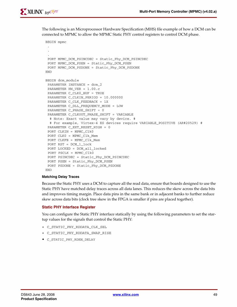
Multi-Port Memory Controller (MPMC) (v4.02.a)
DS643 JuneProduct Sp
The following is an Microprocessor Hardware Specification (MHS) file example of how a DCM can be connected to MPMC to allow the MPMC Static PHY control registers to control DCM phase.
BEGIN mpmc . . . PORT MPMC_DCM_PSINCDEC = Static_Phy_DCM_PSINCDEC PORT MPMC_DCM_PSEN = Static_Phy_DCM_PSEN PORT MPMC_DCM_PSDONE = Static_Phy_DCM_PSDONEEND
BEGIN dcm_module PARAMETER INSTANCE = dcm_2 PARAMETER HW_VER = 1.00.c PARAMETER C_CLK0_BUF = TRUE PARAMETER C_CLKIN_PERIOD = 10.000000 PARAMETER C_CLK_FEEDBACK = 1X PARAMETER C_DLL_FREQUENCY_MODE = LOW PARAMETER C_PHASE_SHIFT = 0 PARAMETER C_CLKOUT_PHASE_SHIFT = VARIABLE
# Note: Exact value may vary by device. ## For example, Virtex-4 ES devices require VARIABLE_POSITIVE (AR#20529) #
PARAMETER C_EXT_RESET_HIGH = 0PORT CLKIN = MPMC_Clk0PORT CLK0 = MPMC_Clk_MemPORT CLKFB = MPMC_Clk_Mem PORT RST = DCM_1_lock
PORT LOCKED = DCM_all_locked PORT PSCLK = MPMC_Clk0 PORT PSINCDEC = Static_Phy_DCM_PSINCDEC PORT PSEN = Static_Phy_DCM_PSEN PORT PSDONE = Static_Phy_DCM_PSDONEEND
Matching Delay Traces
Because the Static PHY uses a DCM to capture all the read data, ensure that boards designed to use the Static PHY have matched delay traces across all data lanes. This reduces the skew across the data bits and improves timing margin. Place data pins in the same bank or in adjacent banks to further reduce skew across data bits (clock tree skew in the FPGA is smaller if pins are placed together).
Static PHY Interface Register
You can configure the Static PHY interface statically by using the following parameters to set the star-tup values for the signals that control the Static PHY:
• C_STATIC_PHY_RDDATA_CLK_SEL
• C_STATIC_PHY_RDDATA_SWAP_RISE
• C_STATIC_PHY_RDEN_DELAY
28, 2008 www.xilinx.com 49ecification

Multi-Port Memory Controller (MPMC) (v4.02.a)
You can then change these values dynamically by using the PLB Control register. Additionally, you can change the phase delay of a DCM that generates MPMC_Clk_Mem using the PLB Control register. The following table describes the Static PHY Interface Register (SPI).
Table 30: Static PHY Interface Register (SPI)
Bit(s) NameCore
AccessReset Value Description
0:3 RDEN_DELAY R/WC_STATIC_PHY_RDEN_DELAY
Sets the number of cycles to delay the read enable (push) to the read FIFOs. See hardware description.
4 RDDATA_CLK_SEL R/WC_STATIC_PHY_RDDATA_CLK_SEL
Sets the read data to be re-registered on the positive or negative edge of MPMC_Clk0: 1 = Positive Edge0 = Negative Edge
5 RDDATA_SWAP_RISE R/WC_STATIC_PHY_RDDATA_SWAP_RISE
Sets the DDR read data to be shifted by 1/2 clock cycle relative to the SDR clock: 0 = no shift 1 = ½ clock cycle shift
6 UNUSED N/A N/A
7 FIRST_RST_DONE R 0Set to 0 during first reset to static PHY; set to 1 afterwards. This prevents the control register from being reset to default values after initial reset.
8 DCM_PSEN R/W 0Set to 1 to perform one DCM phase shift increment or decrement. Self Clearing. Direction of phase shift is determined by DCM_PSINCDEC.
9 DCM_PSINCDEC R/W 0
1 = perform DCM phase shift increments. 0 = perform DCM phase shift decrements. Only valid with DCM_PSEN1 = enable phase shift by +1 tap0 = enable phase shift by -1 tap
10 DCM_DONE R/W 0
Set to 1 when DCM phase shift increment or decrement is complete. This bit must be cleared by MPMC. DCM_PSEN is not set to 1 again until DCM_DONE is set and cleared.
11 INIT_DONE R 0 Set to 1 when initialization is complete; otherwise set to 0.
12:22 UNUSED N/A N/A N/A
23:31 DCM TAP VALUE R 0
9-bit wide two’s complement number (Range -256 to +255). Status of the software-derived DCM tap value. The tap value is relative to the initial phase tap value set in the DCM. The value of this register assumes that the DCM PHASE_SHIFT parameter was initially set to 0; otherwise it reports the relative phase offset only. This value can be incorrect if the DCM phase is shifted beyond the DCM allowable adjustment range.
50 www.xilinx.com DS643 June 28, 2008Product Specification

Multi-Port Memory Controller (MPMC) (v4.02.a)
DS643 JuneProduct Sp
Example Static PHY Calibration Algorithm
The following steps provide a flow chart on how to use the Static PHY Interface PLB control register to calibrate the PHY interface automatically. The software must be run before any other writes or reads are sent to MPMC. Additionally, the software instructions must be stored in block RAM until the MPMC memory is calibrated.
1. Wait for INIT_DONE bit to be set.2. Ensure DCM_TAP_VALUE equals the initial DCM phase shift setting. If it is not equal, stop here,
report error, and rebuild hardware with DCM phase shift set to 0.3. Set DCM phase shift to minimum value using DCM_PSEN, DCM_PSINCDEC, and DCM_DONE.4. Set RDEN_DELAY to 0. (This can cause a processor hang if you are not using port 0 for calibration
reads. If this is the case, you might need to increment the minimum start value and maximum end value for this parameter. See "Static PHY Implementation" page 46 for more details.)
5. Set RDDATA_CLK_SEL to 0.6. Set RDDATA_SWAP_RISE to 0.7. Write pattern to memory with caches turned on.8. Flush and Invalidate cache and read pattern back.9. Increment DCM phase shift, keeping track of how many patterns were read back correctly.10. Repeat [7] through [9] until maximum phase shift value is reached.11. If number of correctly read patterns in a row is greater than an acceptable threshold, repeat steps [7]
through [10] with caches turned off. If number of correctly read patterns in a row is still acceptable, jump to [19].
12. Set RDDATA_SWAP_RISE to 1.13. Repeat steps [7] through [11].14. Set RDDATA_CLK_SEL to 1.15. Repeat steps [6] through [13].16. Increment RDEN_DELAY by 1.17. Repeat steps [5] through [16] until maximum RDEN_DELAY is 0xF.18. If this step is reached, calibration was not possible. Stop here and report error.19. Set DCM phase shift to midpoint of acceptable range using DCM_PSEN, DCM_PSINCDEC, and
DCM_DONE.
Your settings are saved until you power down your board, even if with an MPMC system reset. Ensure that a system reset will not force your DCM phase shift setting to revert back to the initial value. If this is the case, you need to modify your reset structure, rebuild your hardware, and re-run the calibration.
Note: You might wish to build a simple single port MPMC system with a Static PHY, use a software program to characterize the ideal set of static PHY settings for that board, then initialize those settings into the design.
28, 2008 www.xilinx.com 51ecification

Multi-Port Memory Controller (MPMC) (v4.02.a)
52
SDRAM PHY Interface
The SDRAM PHY is the interface between the Single Data Rate Access Memory (SDRAM) and the MPMC control path, address path, and data path. The interface supports Virtex-4, Virtex-5, and Spar-tan-3, (3A/3E/3AN/3ADSP) platforms.
Features
The SDRAM PHY includes the following support features:
• Column Access Strobe (CAS) latencies of 2, 2.5, and 3
• SDRAM data widths of 8, 16, 32, and 64
• DIMMs (both registered and unregistered)
• Multiple Memory Ranks
The PHY interface works from MPMC_Clk0, which issues the control, data, and address signals to mem-ory. To clock SDRAM memory, the PHY uses an inverted version of MPMC_Clk0. This gives a 1/2 clock period setup and hold time for memory control and address signals. Because the PHY works from a single clock source, it simplifies constraining the PHY design.
To drive the data bus with valid data, the memory requirement is CAS_LATENCY – 1 + Tac time (Access Time) after registering the read command. The following figure illustrates the SDRAM read data timing.
The Tac is typically between 5 and 6ns. The data capturing logic works on negedge of MPMC_Clk0. This gives the capturing logic a minimum of 2 ns setup time if memory is running at 133 MHz. The captured data is pushed into the read Data path FIFOs on MPMC_Clk0.
The SDRAM PHY performs the power up initialization sequence and configuration of SDRAM mem-ory with user-specified values from the MHS file.
The required parameter for SDRAM PHY is: C_USE_STATIC_PHY = 0
Figure Top x-ref 5
Figure 6: SDRAM Read Data Timing
DS643_06_071307
T0
READ NOP
CL = 2
NOP
T1 T2 T3
CLK
COMMAND
DQ DOUT
tOHtLZ
tAC
www.xilinx.com DS643 June 28, 2008Product Specification

Multi-Port Memory Controller (MPMC) (v4.02.a)
Connecting Memory to the PHY Interface
The PHY interface permits connections to 8-, 16-, 32-, and 64-bit SDRAM, DDR, or DDR2 memories.
The following table lists the unique signals and parameters for each available PHY layer (excluding standard memory and clock signals):
The memory data and address signals are marked with little-endian labeling.
The following figures (Figure 7 and Figure 8) show the little-endian and big-endian formats. Table 32 on page 55 describes the little-endian bit and byte labeling for the data and control signals in the external memory.
Note: Use caution with the connections to the external memory devices to avoid incorrect data and address connections. The bit ordering used in the MPMC memory interface is reversed from the bit ordering used in the memory controllers named plb_ddr, plb_ddr2, opb_ddr, mch_opb_ddr, and mch_opb_ddr2. A tool such as Base System Builder (BSB) can be used to create MPMC designs to illustrate correct memory interface connections.
Table 31: Signals and Parameters per PHY Layer
PHY Layer Signals Parameters
MIG-Based Virtex-5 DDR2 PHY
MPMC_Clk0_DIV2MPMC_Clk_200MHzMPMC_Idelayctrl_Rdy_I (optional)MPMC_Idelayctrl_Rdy_O (optional)
C_NUM_IDELAYCTRLC_IDELAYCTRL_LOCC_MEM_DQS_IO_COLC_MEM_DQ_IO_MS
MIG-Based Virtex-5 DDR PHYMIG-Based Virtex-4 DDR2 PHYMIG-Based Virtex-4 DDR PHY
MPMC_Clk_200MHzMPMC_Idelayctrl_Rdy_I (optional)MPMC_Idelayctrl_Rdy_O (optional)
C_NUM_IDELAYCTRLC_IDELAYCTRL_LOC
MIG-Based Spartan-3 DDR PHYDDR_DQS_Div_IDDR_DQS_Div_O
N/A
MIG-Based Spartan-3 DDR2 PHYDDR2_DQS_Div_IDDR2_DQS_Div_O
N/A
SDRAM PHY N/A N/A
Static PHY
MPMC_Clk_MemMPMC_DCM_PSENMPMC_DCM_PSINCDECMPMC_DCM_PSDONE
C_STATIC_PHY_RDDATA_CLK_SELC_STATIC_PHY_RDDATA_SWAP_RISEC_STATIC_PHY_RDENDELAY
53 www.xilinx.com DS643 June 28, 2008Product Specification

Multi-Port Memory Controller (MPMC) (v4.02.a)
Figure Top x-ref 6
Figure 7: Little-Endian Memory Data Types
Byte Address n+7
Byte Label 7
Byte Significance 64-bit MemoryMSB
n+6
6
n+5
5
n+4
4
n+3
3
n+2
2
n+1
1
n
0
LSB
Bit Label 31
Bit Significance MSBit
0
LSBit
DS43_56_072607
Byte Address
Byte Label
Byte Significance 32-bit MemoryMSB
n+3
3
n+2
2
n+1
1
n
0
LSB
Bit Label 31
Bit Significance MSBit
0
LSBit
Byte Address
Byte Label
Byte Significance 16-bit MemoryMSB
n+1
1
n
0
LSB
Bit Label 15
Bit Significance MSBit
0
LSBit
Byte Address
Byte Label
Byte Significance 8-bit MemoryMSB
n
0
Bit Label 7
Bit Significance
MS
Bit
0
LSB
it
54 www.xilinx.com DS643 June 28, 2008Product Specification

Multi-Port Memory Controller (MPMC) (v4.02.a)
Little-Endian Label Settings
Table 32: Little-Endian Bit and Byte Label Settings
DescriptionMemory
TypeMPMC Signal [MSB:LSB] Memory Signal [MSB:LSB]
Data Bus All<memory_type>_DQ[C_MEM_DATA_WIDTH-1:0]
DQ[C_MEM_DATA_WIDTH-1:0]
Bank Address All<memory_type>_BankAddr[C_MEM_BANKADDR_WIDTH-1:0]
BA[C_MEM_BANKADDR_WIDTH-1:0]
Address All<memory_type>_Addr[C_MEM_ADDR_WIDTH-1:0]
A[C_MEM_ADDR_WIDTH-1:0]
Data All<memory_type>_DQ[C_MEM_DATA_WIDTH-1:0]
DQ[C_MEM_DATA_WIDTH-1:0]
Data Strobe DDR / DDR2<memory_type>_DQS[C_MEM_DQS_WIDTH-1:0]
UDQS,LDQS (Replicate for number of memory parts)
Differential Data Strobe
DDR2<memory_type>_DQS_n[C_MEM_DQS_WIDTH-1:0]
UDQS#,LDQS# (Replicate for number of memory parts)
Data Mask All<memory_type>_DM[C_MEM_DM_WIDTH-1:0]
UDM,LDM (Replicate for number of memory parts)
ECC Check Bits All
<memory_type>_DQ[C_MEM_DATA_WIDTH+C_MPMC_CTRL_DATA_WIDTH-1:C_MEM_DATA_WIDTH]
DQ_ECC[C_MPMC_CTRL_DATA_WIDTH-1:0]
ECC Data Strobe DDR / DDR2<memory_type>_DQS[C_MEM_DQS_WIDTH+C_MPMC_CTRL_DQS_WIDTH-1:C_MEM_DQS_WIDTH]
DQS_ECC[C_MPMC_CTRL_DQS_WIDTH-1:0]
Differential ECC Data Strobe
DDR2
<memory_type>_DQS_n[C_MEM_DQS_WIDTH+C_MPMC_CTRL_DQS_WIDTH-1:C_MEM_DQS_WIDTH]
DQSn_ECC[C_MPMC_CTRL_DQS_WIDTH-1:0]
ECC Data Mask All
<memory_type>_DM[C_MEM_DM_WIDTH+C_MPMC_CTRL_DM_WIDTH-1:C_MEM_DM_WIDTH]
DM_ECC[C_MPMC_CTRL_DM_WIDTH-1:0]
55 www.xilinx.com DS643 June 28, 2008Product Specification
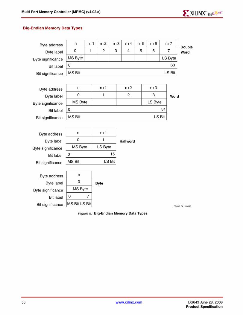
Multi-Port Memory Controller (MPMC) (v4.02.a)
Big-Endian Memory Data Types
Figure Top x-ref 7
Figure 8: Big-Endian Memory Data Types
n n+1 n+2 n+3
0 1 2 3
MS Byte LS Byte
0 31
Byte address
Byte label
Byte significance
Bit label
Bit significance
n n+1
0 1
MS Byte LS Byte
0 15
MS Bit
MS Bit
LS Bit
Byte address
Byte label
Byte significance
Bit label
Bit significance
n
0
MS Byte
DS643_64_103007
0 7
Byte address
Byte label
Byte significance
Bit label
Bit significance
Byte
Halfword
Word
n
0 1 2
MS Byte LS Byte
0 63
Byte address
Byte label
Byte significance
Bit label
Bit significance MS Bit LS Bit
MS Bit LS Bit
LS Bit
Word
n+1 n+2 n+3 n+4 n+5 n+6 n+7
3 4 5 6 7Double
56 www.xilinx.com DS643 June 28, 2008Product Specification

Multi-Port Memory Controller (MPMC) (v4.02.a)
Connecting Memory to a DDR2 MPMC Design Example
The following figure illustrates an example of connecting memory to a DDR2 MPMC design.
Figure 9: Example DDR2 Memory Connections
DDR2_DQ[63:48] DQ[15:0] DDR2Memory #1
x16
Rank 1
DDR2_CS_n[1]
DDR2_DQS[7:6] UDQS, LDQSDDR2_DQS_n[7:6] UDQS#, LDQS#
DDR2_DM[7:6] UDM, LDM
DDR2_DQ[47:32] DQ[15:0] DDR2Memory #2
x16DDR2_DQS[5:4] UDQS, LDQS
DDR2_DQS_n[5:4] UDQS#, LDQS#DDR2_DM[5:4] UDM, LDM
DDR2_DQ[31:16] DQ[15:0] DDR2Memory #3
x16DDR2_DQS[3:2] UDQS, LDQS
DDR2_DQS_n[3:2] UDQS#, LDQS#DDR2_DM[3:2] UDM, LDM
DDR2_DQ[15:0] DQ[15:0] DDR2Memory #4
x16DDR2_DQS[1:0] UDQS, LDQS
DDR2_DQS_n[1:0] UDQS#, LDQS#DDR2_DM[1:0] UDM, LDM
DDR2_DQ[71:64] DQ[7:0] DDR2Memory #5
x16DDR2_DQS[8] LDQS
DDR2_DQS_n[8] LDQS#DDR2_DM[8]
DDR2_BankAddr[1:0]
DDR2_Addr[12:0]
DDR2_Clk[0]
DDR2_Clk_n[0]
DDR2_CE[0]
DDR2_RAS/CAS/WE
DDR2_ODT[0]
LDMDQ[15:8]UDQSUDQS#UDM
DDR2_DQ[63:48] DQ[15:0] DDR2Memory #6
x16
Rank 2
DDR2_CS_n[0]
DDR2_DQS[7:6] UDQS, LDQSDDR2_DQS_n[7:6] UDQS#, LDQS#
DDR2_DM[7:6] UDM, LDM
DDR2_DQ[47:32] DQ[15:0] DDR2Memory #7
x16DDR2_DQS[5:4] UDQS, LDQS
DDR2_DQS_n[5:4] UDQS#, LDQS#DDR2_DM[5:4] UDM, LDM
DDR2_DQ[31:16] DQ[15:0] DDR2Memory #8
x16DDR2_DQS[3:2] UDQS, LDQS
DDR2_DQS_n[3:2] UDQS#, LDQS#DDR2_DM[3:2] UDM, LDM
DDR2_DQ[15:0] DQ[15:0] DDR2Memory #9
x16DDR2_DQS[1:0] UDQS, LDQS
DDR2_DQS_n[1:0] UDQS#, LDQS#DDR2_DM[1:0] UDM, LDM
DDR2_DQ[71:64] DQ[7:0] DDR2Memory #10
x16DDR2_DQS[8] LDQS
DDR2_DQS_n[8] LDQS#DDR2_DM[8] LDM
DQ[15:8]UDQSUDQS#UDM
DS43_57_072607
57 www.xilinx.com DS643 June 28, 2008Product Specification

Multi-Port Memory Controller (MPMC) (v4.02.a)
58
The example in Figure 9 on page 57 has the following specified parameters:
C_MEM_TYPE = “DDR2”C_INCLUDE_ECC_SUPPORT = 1C_MEM_CLK_WIDTH = 1C_MEM_ODT_WIDTH = 2C_MEM_CE_WIDTH = 1C_MEM_CS_N_WIDTH = 2C_MEM_ADDR_WIDTH = 13C_MEM_BANKADDR_WIDTH = 2C_MEM_DATA_WIDTH = 64C_MEM_NUM_RANKS = 2C_MEM_NUM_DIMMS = 1
In this example:
• The DDR2_CS_n[0] signal is connected to one rank of memory and DDR2_CS_n[1] is connected to the other rank of memory. The DDR2_ODT[0] signal is connected to one rank of memory and DDR2_ODT[1] is connected to the other rank of memory.
• Within a particular rank, the signals DDR2_CS_n[?] and DDR2_ODT[?] are connected to each memory in the rank. Some memory manufactures have specific recommendations for how these signals should be connected. For example, when using a dual rank DIMM, the recommendation might be to assert DDR2_ODT on the same rank that DDR2_CS_n is asserted (as shown in Figure 9 on page 57). Other recommendations might be to assert DDR2_ODT on to opposite rank that the DDR2_CS_n is asserted, which can be achieved by swapping DDR2_ODT[0] and DDR2_ODT[1].
• All clock, addresses, and other control signals are also connected to each memory.
• The DDR2_DQ, DDR2_DQS, DDR2_DQS_n, and DDR2_DM signals do not go to all discrete memory components. Instead, 16 bits of DDR2_DQ go to one memory in each rank and 2 bits of DDR2_DQS, DDR2_DQS_n, and DDR2_DM go to one memory in each rank. The only exception is the ECC memory. When C_MEM_DATA_WIDTH is set to 64, there are 8 ECC bits. Because the memory has 16 bits; 8 of the DQ bits, the UDQS, the UDQS numbers, and the UDM are left unconnected. All other pins are connected on the memory.
The parameters C_MEM_CLK_WIDTH, C_MEM_CE_WIDTH, C_MEM_CS_N_WIDTH, and C_MEM_ODT_WIDTH can be used to replicate the CLK, CKE, CSn, and ODT outputs of MPMC to match the board schematics. Care must be taken with C_MEM_CS_N_WIDTH and C_MEM_ODT_WIDTH as these parameters must be an integer multiple of C_NUM_RANKS*C_NUM_DIMMS.
www.xilinx.com DS643 June 28, 2008Product Specification

Multi-Port Memory Controller (MPMC) (v4.02.a)
DS643 JuneProduct Sp
IDELAY Controller
For Virtex-4 and Virtex-5 systems using the MIG PHY, instantiation of IDELAY controllers (IDELAYC-TRL) is required to ensure that the IDELAY elements in the MPMC physical interface behave properly. The MPMC core parameter, C_NUM_IDELAYCTRL, determines the number of IDELAYCTRL elements to instantiate. By default, the MPMC instantiates one IDELAYCTRL without a location constraint (LOC), which causes the ISE implementation tools to replicate the IDELAYCTRL blocks across the entire FPGA.
Single MPMC Designs
For Virtex-5 designs and Virtex-4 designs with the MAP-timing option enabled, MAP will trim unnec-essary IDELAYCTRLs. The default setting is sufficient for systems where there is one MPMC instance only, and no other IP in the system requires the use of IDELAY elements.
Multiple MPMC / IDELAYCTRL IP Designs
For systems where there are multiple IP cores each using their own IDELAYCTRL element indepen-dently, such as two instances of MPMC or MPMC and PCI in the same system, special consideration must be given to the number of IDELAYCTRLs.
• Instantiate the correct number of IDELAYCTRL blocks for each IP as determined by the clock regions where the associated IDELAY elements are used. For these systems, it is necessary to set the correct value for C_NUM_IDELAYCTRL.
• Ensure the IDELAYCTRL element is associated with the correct clock region positions in the FPGA and is located using the C_IDELAYCTRL_LOC parameter.
For example, a design requiring two IDELAYCTRLs might have a core configuration of:
PARAMETER C_NUM_IDELAYCTRL = 2PARAMETER C_IDELAYCTRL_LOC = IDELAYCTRL_X0Y4-IDELAYCTRL_X1Y3
Consult the ISE documentation for more information about IDELAYCTRL. The link to ISE documenta-tion is available in “Reference Documents,” page 163.
MPMC contains the following ports (see Table 10 on page 14) that can be used to chain the IDELAY ele-ments between IP blocks:
• MPMC_Idelayctrl_Rdy_I is AND’d with internal IDELAYCTRL RDY signals inside MPMC and signifies that memory initialization can begin.
• MPMC_Idelayctrl_Rdy_O port signals that the internal IDELAYCTRL RDY signals and the MPMC_Idelayctrl_Rdy_I are all high.
This is useful in situations where two IP blocks have I/O that share a common clock region and IDE-LAYCTRL element. You can connect the MPMC_Idelayctrl_Rdy_O to the MPMC_Idelayctrl_Rdy_I of downstream MPMC IP or other IP blocks.
Additionally, the MPMC_Idelayctrl_RDY_0 outputs of upstream IP blocks with IDELAYCTRL can be tied to the MPMC_Idelayctrl_Rdy_I input.
• Ensure that the MPMC_Idelayctrl_Rdy_I and MPMC_Idelayctrl_Rdy_O ports are not connected in a circular manner over one or more IP blocks.
• MPMC_Idelayctrl_Rdy_I and MPMC_Idelayctrl_Rdy_O can be left unconnected when not needed. The EDK XPS tool ties MPMC_Idelayctrl_Rdy_I to high automatically when it is unconnected.
28, 2008 www.xilinx.com 59ecification

Multi-Port Memory Controller (MPMC) (v4.02.a)
60
Clock and Reset Logic
MPMC has four system clock inputs and one clock for each PIM. Depending on the MPMC configura-tion, not all system clocks must be connected.
Note: For behavioral simulation, the MPMC_Clk and all <PIM>_Clks must be completely phase-aligned. This requirement is not as strict for actual implementation as any clock skew will be correctly analyzed by static timing analysis tools.
The basic MPMC core and each of the MPMC PIMs have a reset input. Internally these resets are OR’ed together to create the master reset for the entire MPMC (including PIMs).
Note: It is not possible to reset an individual PIM or PORT of the MPMC without resetting everything.
The master reset is internally registered and synchronized before being distributed throughout MPMC; therefore, the MPMC reset is a fully synchronous reset. Reset should be held for a minimum of eight cycles of the slowest PIM clock. After reset, there should not be access to any of the ports or control interfaces for 20 cycles of the MPMC_Clk. The following table provides a summary of the clocks and resets.
See the "System I/O Signals" page 14 for more information on clocks and reset signals.
Table 33: Clock and Reset Summary
Clock/Reset Name Description
MPMC_Clk0 Main MPMC clock; used to generate memory clock.
MPMC_Clk0_DIV2 MPMC_Clk0, divided by 2; used in MIG-based Virtex-5 DDR2 PHY only.
MPMC_Clk90 Main MPMC clock, phase shifted by 90 degrees.
MPMC_Clk_200MHz200 MHz clock; used in Virtex-4 and Virtex-5 architectures for IDELAY Control logic only. Only valid when using MIG-based Virtex-4/Virtex-5 DDR/DDR2 PHY.
MPMC_Clk_MemMain MPMC clock, phase-shifted by n degrees. Used with Static PHY Interface only. See "Static PHY Interface" page 46 for more details
<PIM>_Clk
See specific PIM documentation for more details. Generally, these clocks will be the same as MPMC_Clk, or the MPMC_Clk synchronously divided by 2. The XCL, PLB, and SDMA PIMs support only 1:1 or 1:2 synchronous clock ratios. The XCL and PLB PIMs will detect automatically which clock ratio is being used. The SDMA requires that the clock ratio be specified by the C_SDMA<Port_Num>_PI2LL_CLK_RATIO parameter.
MPMC_Rst Main MPMC reset.
<PIM>_Rst See specific PIM documentation for more details.
www.xilinx.com DS643 June 28, 2008Product Specification

Multi-Port Memory Controller (MPMC) (v4.02.a)
DS643 JuneProduct Sp
Transaction Ordering and Memory Coherency
In the MPMC architecture, transactions are executed to memory in the order that the transactions are acknowledged with respect to a single port; consequently, on a single port, transactions are completed in the same order as requested.
Across multiple ports of MPMC there is no guarantee that the transactions issued by different ports will complete in the request order. You can modify the arbitration algorithms so that a given port is favored over another port. This can be used as a mechanism to influence transaction ordering but might not guarantee a specific order.
MPMC allows write transactions to be buffered inside the MPMC. Because of the buffering, there is an undefined time between when a write transaction has completed over NPI and when the write com-pletes to memory.
Because transaction ordering is not guaranteed across ports, a port doing a read from an address loca-tion being written to by another port might read the new or the old memory value. In some applica-tions it is important to know that a write has completed to memory before issuing a read of that location.
There are three methods that can ensure coherency:
1. The NPI interface can monitor the Write FIFO empty flag:- The empty flag is asserted when the write has completed to memory.
- The design can wait for the empty flag to go high before signaling that a read can be performed.
2. The design can take advantage of the fact that transactions complete in order on a given port:- After a write to a sensitive part of memory, the device can issue a dummy read and wait for the
dummy read to complete and return data.
- The completion of the dummy read ensures that the previous write has completed to memory.
3. The arbitration algorithm can be adjusted:- If the port performing the writes can always be set to have higher priority than the ports doing
the reads, this should also ensure that the write completes before the read across the two ports. Care should be taken with this method if there is a possibility that the PIM can have “bubble” cycles between the write and the read request.
Note: Using any of these methods to ensure coherency could result in reduced system performance; employ these methods when necessary only.
The DPLB and PLB PIMs follow the PLB CoreConnect method for handling memory coherency (for example, between PowerPC 405 processor instruction and data PLB interface). The PLB BUSY signal is asserted on writes until the Write_FIFO_Empty flag is asserted indicating the write transaction has completed to memory. The processor normally ignores the BUSY flag unless an instruction is executed such as Sync or Enforce Instruction Execution In Order (EIEIO). When the Sync or EIEIO instruction is executed, the processor waits for PLB BUSY to be de-asserted before issuing another transaction.
28, 2008 www.xilinx.com 61ecification

Multi-Port Memory Controller (MPMC) (v4.02.a)
62
Personality Interface ModulesPersonality Interface Module Introduction
The Personality Interface Module (PIM) architecture comprises the following interfaces:
• "Xilinx CacheLink"
• "Soft Direct Memory Access Controller for LocalLink Interfaces"
• "Processor Local Bus Version 4.6 PIM"
• "Native Port Interface PIM"
• "PowerPC 440 Memory Controller PIM"
• "Video Frame Buffer Controller PIM"
The following subsections describe the PIMs. The PIM design parameters, I/O signals, and control and status register summaries are in "Design Parameters" page 2, "MPMC I/O Signals" page 14, and "Con-trol and Status Registers" page 27, respectively.
Note: Throughout the document, the size of a word is 32-bits.
www.xilinx.com DS643 June 28, 2008Product Specification

Multi-Port Memory Controller (MPMC) (v4.02.a)
DS643 JuneProduct Sp
Xilinx CacheLink
The Xilinx CacheLink (XCL) PIM as shown in the following figure:
• Supports XCL requests for 1-, 4-, 8-, or 16-word reads and Writes (user-configurable parameter).
• Connects an XCL interface to the MPMC processor core (pcore).
• Contains the logic to respond to any slave-side XCL transaction emitted by the MicroBlaze soft processor.
• Supports configurable pipeline stages for latency versus frequency trade-offs.
Connecting the XCL BusWhen you connect the XCL bus to a MicroBlaze processor the IXCL and DXCL paths between Micro-Blaze and MPMC are optimized. In this case, the parameter C_PIM<Port_Num>_SUBTYPE would be auto-calculated by XPS to have the value IXCL or DXCL.The FSL Read FIFO is optimized by assuming the Read_Data_Read signal will be asserted in the same cycle as Read_Data_Exists.
The IXCL path is additionally optimized by effectively setting C_WRITEXFER = 0, thus eliminated the write path inside the PIM and the write FIFO logic inside MPMC. These modes of operation can be emulated by setting the C_PIM<Port_Num>_SUBTYPE to DXCL or IXCL to emulate the simplifications when you are not connected to a MicroBlaze processor.
XCL Line Size and Write Transfers
The parameter C_XCL<Port_Num>_LINESIZE specifies whether the XCL line size is 1, 4, 8, or 16 words. This line size is set for all XCL reads. 4-, 8-, or 16-word transfers are target word first cacheline transfers.
For writes, the parameter C_XCL<Port_Num>_WRITEXFER specifies whether XCL Write transactions are:
• Disabled (0)
• 1 word only (1)
• The same size as the reads C_XCL<Port_Num>_LINESIZE (2)
If the XCL PIM is used, the NPI data width is fixed at 32 bits automatically. XCL data and address are labeled with big-endian bit/byte ordering as described in Figure 8 on page 56.
Figure Top x-ref 8
Figure 10: MicroBlaze XCL Block Diagram
Access FSL Signals
Read Data FSL SignalsNPI Signals
CombinatorialLogic
FIFO
FIFO
DS643_52_071307
NPI XCL
28, 2008 www.xilinx.com 63ecification

Multi-Port Memory Controller (MPMC) (v4.02.a)
64
XCL Pipeline Stages
The C_XCL<Port_Num>_PIPE_STAGES parameter can be used to adjust the number of pipeline stages in the XCL PIM. There are 3 different pipelines with 4 possible settings for C_XCL<Port_Num>_PIPE_STAGES:
• 0 - No pipelines enabled.
• 1 - One pipeline enabled: Adds the pipeline on the output of the XCL Read Data FIFO.
• 2 - Two pipelines enabled: Adds the first pipeline on the XCL Read Data FIFO and another, new pipeline on the NPI Read FIFO Empty signal.
• 3 - All pipelines enabled: Enables the pipelines on XCL Read Data FIFO, NPI Read FIFO Empty, and another pipeline on the output of the XCL Access FIFO.
Note: Pipelines added in with values 1 and 2 each add a cycle of latency to each XCL Read. The pipeline added with value 3 might add one cycle of latency to both XCL Reads and XCL Writes.
For additional details on XCL, see the MicroBlaze Processor Reference Guide. The "Reference Documents" page 163 contains a link to the document.
XCL Clock Requirements
The XCL PIM runs at an integer ratio of the MPMC memory clock rate. This clock ratio is automatically detected during reset and can be a ratio of either 1:1 or 2:1.
The XCL PIM clock must be synchronous and rising edge-aligned to the MPMC memory clock.
www.xilinx.com DS643 June 28, 2008Product Specification

Multi-Port Memory Controller (MPMC) (v4.02.a)
DS643 JuneProduct Sp
Soft Direct Memory Access Controller for LocalLink Interfaces
The Soft Direct Memory Access (SDMA) Controller PIM provides high-performance Direct Memory Access (DMA) for streaming data. The SDMA provides two channels, one for receiving data and one for transmitting data. Transmit and Receive is accomplished through two LocalLink interfaces. SDMA is a PIM integrated into MPMC.
Features
The SDMA Controller for LocalLink interfaces contains the following features:
• Direct plug-in to MPMC
• Simultaneous, independent Transmit and Receive DMA operations
• Per-channel Interrupt Event reporting
• Interrupt Coalescing
• Xilinx PLBv4.6 interface for control as a register access
• User-defined LocalLink headers and footers1
• Dynamic Scatter Gather Buffer Descriptor modification
System Diagram
The SDMA uses a Native Port Interface (NPI), two LocalLink interfaces, and a PLB interface. The NPI connects the SDMA controller into the MPMC PIM. The two LocalLink interfaces, a Transfer (TX) and a Receive (RX), provide full duplex LocalLink device access to the SDMA. The PLB interface allows the CPU to interact with the SDMA for initiating DMA processes or status gathering. The PLB and LocalL-ink data and address signals are labelled with big-endian bit/byte ordering as described in Figure 8 on page 56. The following figure provides a high-level block diagram of SDMA.
1. For use with functions such as checksum off loading
Figure Top x-ref 9
Figure 11: High Level SDMA Block Diagram
DS643_08_082207
DMA Engine andControl Logic
TX LocalLinkInterface
RX LocalLinkInterface
RX LocalLink
NPI SignalsNPI
PLB
SDMAplbv46_slave_single
TX LocalLink
28, 2008 www.xilinx.com 65ecification
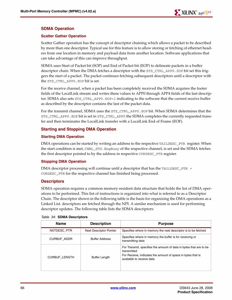
Multi-Port Memory Controller (MPMC) (v4.02.a)
66
SDMA Operation
Scatter Gather Operation
Scatter Gather operation has the concept of descriptor chaining which allows a packet to be described by more than one descriptor. Typical use for this feature is to allow storing or fetching of ethernet head-ers from one location in memory and payload data from another location. Software applications that can take advantage of this can improve throughput.
SDMA uses Start of Packet bit (SOP) and End of Packet bit (EOP) to delineate packets in a buffer descriptor chain. When the DMA fetches a descriptor with the STS_CTRL_APP0.SOP bit set this trig-gers the start of a packet. The packet continues fetching subsequent descriptors until a descriptor with the STS_CTRL_APP0.EOP bit is set.
For the receive channel, when a packet has been completely received the SDMA acquires the footer fields of the LocalLink stream and writes these values to APP0 through APP4 fields of the last descrip-tor. SDMA also sets STS_CTRL_APP0.EOP=1 indicating to the software that the current receive buffer as described by the descriptor contains the last of the packet data.
For the transmit channel, SDMA uses the STS_CTRL_APP0.EOP bit. When SDMA determines that the STS_CTRL_APP0.EOP bit is set in STS_CTRL_APP0 the SDMA completes the currently requested trans-fer and then terminates the LocalLink transfer with a LocalLink End of Frame (EOF).
Starting and Stopping DMA Operation
Starting DMA Operation
DMA operations can be started by writing an address to the respective TAILDESC_PTR register. When the start condition is met, CHNL_STS.EngBusy of the respective channel, is set and the SDMA fetches the first descriptor pointed to by the address in respective CURDESC_PTR register.
Stopping DMA Operation
DMA descriptor processing will continue until a descriptor that has the TAILDESC_PTR = CURDESC_PTR for the respective channel has finished being processed.
Descriptors
SDMA operation requires a common memory-resident data structure that holds the list of DMA oper-ations to be performed. This list of instructions is organized into what is referred to as a Descriptor Chain. The descriptor shown in the following table is the basis for organizing the DMA operations as a Linked List. descriptors are fetched through the NPI. A similar mechanism is used for performing descriptor updates. The following table lists the SDMA descriptors:
Table 34: SDMA Descriptors
Name Description Purpose
NXTDESC_PTR Next Descriptor Pointer Specifies where in memory the next descriptor is to be fetched
CURBUF_ADDR Buffer AddressSpecifies where in memory the buffer is for receiving or transmitting data
CURBUF_LENGTH Buffer Length
For Transmit, specifies the amount of data in bytes that are to be transmittedFor Receive, indicates the amount of space in bytes that is available to receive data
www.xilinx.com DS643 June 28, 2008Product Specification

Multi-Port Memory Controller (MPMC) (v4.02.a)
DS643 JuneProduct Sp
The following table shows the STS_CTRL_APP0 register bits.
Each field of the descriptor is 4 bytes in length and corresponds to either one of the DMA channel reg-isters or user application fields.
• For transmit channels, the application data fields (App0 to App4) of the first descriptor are transmitted as part of the Header of the LocalLink Transmit Data stream.
• For receive channels, the Application Data Fields of the last buffer descriptor will be updated with a portion of the Footer of the LocalLink Receive Data stream.
See "LocalLink Headers and Footers" page 77 for more information on LocalLink headers and footers.
Figure 12 on page 68 shows descriptors organized into a linked list. SDMA will successively perform the DMA operations specified in the descriptors up to and including the descriptor with the CURDESC_PTR = TAILDESC_PTR.
Name Description Purpose
STS_CTRL_APP0Status/Control and
App Data 0
Status/Control for controlling and providing status to the DMA transferFor Transmit, App0 is used for application specific dataFor Receive, App0 is not used
APP1 Application Data 1 Application specific data
APP2 Application Data 2 Application specific data
APP3 Application Data 3 Application specific data
APP4 Application Data 4 Application specific data
Table 35: STS_CTRL_APP0
Bit(s) Name Type Description
0 Error Status Set by the DMA when a error is encountered.
1 IrqOnEnd ControlWhen set, causes the DMA to generate an interrupt event when the current descriptor has been completed.
2 Reserved N/A Undefined
3 Completed Status When set, indicates that the current descriptor has been completed.
4 SOP Status/Control
Transmit Channel (Control): Set by software in the descriptor indicating this buffer descriptor is the first descriptor of a packet.Receive Channel: (Status) Set by DMA in the descriptor indicating that a start of packet was received on LocalLink.
5 EOP Status/Control
Transmit Channel (Control): Set by software in the descriptor indicating this buffer descriptor is the last descriptor of a packet.Receive Channel (Status): Set by DMA in the descriptor indicating that an end of packet was received on LocalLink.
6 EngBusy StatusWhen set, indicates that the DMA is processing buffer descriptors. This bit a copy of the corresponding bit in the CHANNEL_STS register.
7 Reserved N/A Undefined
8:31 Application Data 0 N/A Application specific data.
Table 34: SDMA Descriptors (Continued)
28, 2008 www.xilinx.com 67ecification

Multi-Port Memory Controller (MPMC) (v4.02.a)
68
Figure 13 on page 69 shows descriptors organized into a buffer ring. The buffer ring is for a Transmit channel as evidenced by STS_CTRL_APP0.SOP=1 and STS_CTRL_APP0.EOP=1 tags. Note that packet 4 is specified by a single descriptor and others by more than one consecutive descriptor. The address of the last ready packet is equal to the TAILDESC_PTR, giving a sentinel position in the ring.
Note: Even if descriptors are contiguously allocated, they are required to be linked through the NXTDESC_PTR field.
Figure Top x-ref 10
Figure 12: Linked List of Descriptors
NXTDESC_PTR
CURBUF_ADDR
CURBUF_LENGTH
STS_CTRL_APP0
APP1
APP2
APP3
APP4
NXTDESC_PTR
CURBUF_ADDR
CURBUF_LENGTH
STS_CTRL_APP0
APP1
APP2
APP3
APP4
NXTDESC_PTR
CURBUF_ADDR
CURBUF_LENGTH
STS_CTRL_APP0
APP1
APP2
APP3
APP4
NXTDESC_PTR
CURBUF_ADDR
CURBUF_LENGTH
STS_CTRL_APP0
APP1
APP2
APP3
APP4
NXTDESC_PTR
CURBUF_ADDR
CURBUF_LENGTH
STS_CTRL_APP0
APP1
APP2
APP3
APP4
NXTDESC_PTR
CURBUF_ADDR
CURBUF_LENGTH
STS_CTRL_APP0
APP1
APP2
APP3
APP4
NXTDESC_PTR
CURBUF_ADDR
CURBUF_LENGTH
STS_CTRL_APP0
APP1
APP2
APP3
APP4
NXTDESC_PTR
CURBUF_ADDR
CURBUF_LENGTH
STS_CTRL_APP0
APP1
APP2
APP3
APP4DS643_18_071307
CURDESC_PTRRegister Value
Address of thisDescriptor = TAILDESC_PTR
www.xilinx.com DS643 June 28, 2008Product Specification

Multi-Port Memory Controller (MPMC) (v4.02.a)
DS643 JuneProduct Sp
Note: For receive channels, STS_CTRL_APP0.SOP and STS_CTRL_APP0.EOP are set by SDMA and updated to memory for use by the software application.
Figure Top x-ref 11
Figure 13: Descriptors Organized Into a Buffer Ring
NXTDESC_PTR
CURBUF_ADDR
CURBUF_LENGTH
STS_CTRL_APP0
APP1
APP2
APP3
APP4
NXTDESC_PTR
CURBUF_ADDR
CURBUF_LENGTH
STS_CTRL_APP0
APP1
APP2
APP3
APP4
NXTDESC_PTR
CURBUF_ADDR
CURBUF_LENGTH
STS_CTRL_APP0
APP1
APP2
APP3
APP4
NXTDESC_PTR
CURBUF_ADDR
CURBUF_LENGTH
STS_CTRL_APP0
APP1
APP2
APP3
APP4
NXTDESC_PTR
CURBUF_ADDR
CURBUF_LENGTH
STS_CTRL_APP0
APP1
APP2
APP3
APP4
NXTDESC_PTR
CURBUF_ADDR
CURBUF_LENGTH
STS_CTRL_APP0
APP1
APP2
APP3
APP4
NXTDESC_PTR
CURBUF_ADDR
CURBUF_LENGTH
STS_CTRL_APP0
APP1
APP2
APP3
APP4
NXTDESC_PTR
CURBUF_ADDR
CURBUF_LENGTH
STS_CTRL_APP0
APP1
APP2
APP3
APP4
DS643_19_071307
CURDESC_PTRRegister Value
SOP =1 and EOP = 1Descriptor Address =TAILDESC_PTR
SOP =1
EOP =1
SOP =1
SOP =1
EOP =1
EOP =1
Packet 4
Packet 2
Packet 3Packet 1
28, 2008 www.xilinx.com 69ecification

Multi-Port Memory Controller (MPMC) (v4.02.a)
70
Transmit Channel Operation
The following is a list of steps required to execute a packet transmit operation:
1. Software creates a chain of descriptors:a. Specify in the descriptor the packet boundaries using the STS_CTRL_APP0.SOP and
STS_CTRL_APP0.EOP bits.b. Specify the address to the data buffer to transmit in the CURBUF_ADDR Field.c. Specify the amount of data to transfer for each descriptor in the CURBUF_LENGTH Field.d. Specify a pointer to the next descriptor in NXTDESC_PNT.
2. Software prepares the DMA Channel Registers (Order of steps [a] and [b] are not critical):a. Set up interrupts if so desired by writing to the TX_CHNL_CTRL register, specifying interrupt
coalescing information (if enabled).b. Set a pointer to the first descriptor in the TX_CURDESC_PTR register.
3. Software starts SG Automation by writing the pointer to the last descriptor to fetch into the TAILDESC_PTR register.
4. SDMA requests the first descriptor pointed to by the TX_CURDESC_PTR register. 5. Upon completion of the descriptor fetch, the DMA cycle begins.6. If the currently fetched descriptor has STS_CTRL_APP0.EOP set, the data of that descriptor is
transmitted and the Master completes the packet on the LocalLink with and End of Payload, (EOP) and End of Frame (EOF). If the currently fetched descriptor does NOT have STS_CTRL_APP0.EOP set the packet continues.
7. At the completion of each descriptor the channel register information is updated to the corresponding descriptor memory location.
8. This process continues until the descriptor TX_CURDESC_PTR = TX_TAILDESC_PTR is completed processing.
www.xilinx.com DS643 June 28, 2008Product Specification

Multi-Port Memory Controller (MPMC) (v4.02.a)
DS643 JuneProduct Sp
Receive Channel Operation
The following is a list of steps required to execute a receive operation:
1. Software creates a chain of descriptors.
Note: SDMA supports multiple descriptors being used to describe a single packet. The STS_CTRL_APP0.EOP bit is set by SDMA in the descriptor associated to the buffer containing the last byte of the received packet.
a. Specify in the CURBUF_ADDR field of each descriptor the address to the start of the associated buffer for receiving data.
b. Specify in the CURBUF_LENGTH field of each descriptor the available size of the associated buffer for receiving data. The sum total of the Length field/s in the descriptors must specify a byte count that is large enough to hold an entire packet.
c. Specify a pointer to the next descriptor in NXTDESC_PNT field.2. Software prepares the DMA Channel registers (Order of steps [a] and [b] are not critical):
a. Set the pointer to the first descriptor in RX_CURDESC_PTR register.b. Set up Interrupts if required by writing to the RX_CHNL_CTRL register, specifying interrupt
coalescing information (if enabled).3. Software starts SG Automation by writing the pointer to the last descriptor to fetch into the
RX_TAILDESC_PTR register.4. SDMA requests the first descriptor pointed to by the RX_NXTDESC_PTR register. For receive
channels, the User Application fields is updated in the descriptor during the descriptor update phase of processing.
5. Upon completion of the descriptor fetch, the DMA cycle begins.
This process continues until the descriptor RX_CURDESC_PTR = RX_TAILDESC_PTR has completed processing.
Error Conditions
SDMA performs several error checking functions to ensure proper operation of the DMA engine. If an error occurs then the channel on which the error is detected is halted, and the channel status register Error bit for the channel is set to 1. If possible, the Error bit for the current descriptor is set to 1 also; although, depending on the error condition, this might not get updated to remote memory.
To recover from an error condition the SDMA must be reset either by a hard reset or by issuing a soft reset (such as setting SwReset = 1 in the DMA Control register.
28, 2008 www.xilinx.com 71ecification

Multi-Port Memory Controller (MPMC) (v4.02.a)
72
The following table lists the possible errors that can be flagged and their causes:
Table 36: Descriptor Errors
Errors Descriptions
TX_CHNL_STS.CurPErr RX_CHNL_STS.CurPErr
Current Descriptor Pointer ErrorThis error occurs if the Current Descriptor Pointer does not fall within the <prefix>_BASEADDR to <prefix>_HIGHADDR range(1). Descriptors must reside within memory as mapped by the base address and high address of the NPI. Addresses outside this range are detected and flagged as errors.
TX_CHNL_STS.TailPErr RX_CHNL_STS.TailPErr
Tail Descriptor Pointer Error This error occurs if the Tail Descriptor Pointer does not fall within the <prefix>_BASEADDR to <prefix>_HIGHADDR range. Descriptors must reside within memory as mapped by the base address and high address of the NPI. Addresses outside this range are detected and flagged as errors.
TX_CHNL_STS.NxtPErr RX_CHNL_STS.NxtPErr
Next Descriptor Pointer ErrorThis error occurs if the Next Descriptor Pointer does not fall within the <prefix>_BASEADDR to <prefix>_HIGHADDR range(1). Descriptors must reside within memory as mapped by the base address and high address of the NPI Addresses outside this range are detected and flagged as errors.
TX_CHNL_STS.AddrErr RX_CHNL_STS.AddrErr
Buffer Address Error This error occurs if the Buffer Address does not fall within the <prefix>_BASEADDR to <prefix>_HIGHADDR range(1). All transmit and receive data buffers must reside within memory as mapped by the base address and high address of the NPI.Addresses outside this range are detected and flagged as errors.
TX_CHNL_STS.CmpErr RX_CHNL_STS.CmpErr
Complete Bit ErrorThis error occurs if a descriptor is fetched with the Complete bit set to 1 (as in STS_CTRL_APP0.Completed=1). This error indicates that a descriptor, which had been already used by SDMA, is being processed again, before the software application has had a chance to process the descriptor and associated data buffer. This error checking can be disabled or enabled by setting/clearing C_COMPLETED_ERR_TX and C_COMPLETED_ERR_RX for the associated channel. Setting the parameters to 1 enables checking and setting the parameters to 0 disables checking.
TX_CHNL_STS.BsyWr RX_CHNL_STS.BsyWr
Busy Write Error This error occurs if the Current Descriptor Pointer register is written to via the PLB v4.6 slave port while the SDMA engine is busy. Examining TX_CHNL_STS.EngBusy and RX_CHNL_STS.EngBusy for the respective channel will indicate to the software application whether or not the channel is busy. If EBsy = 1 then the channel is busy and The Current Descriptor Pointer should not be written to by the software application.
1. where: C_ALL_PIMS_SHARE_ADDRESSES =0: <prefix> = C_MPMC1: <prefix> = C_PIM<Port_Num>
www.xilinx.com DS643 June 28, 2008Product Specification

Multi-Port Memory Controller (MPMC) (v4.02.a)
DS643 JuneProduct Sp
Managing Descriptors
Prior to starting DMA operations, the software application must set up a descriptor or chain of descrip-tors. After the descriptors are set, SDMA begins processing the descriptors, fetches, processes, and then updates the descriptors. By analyzing the descriptors, the software application can read status on the associated DMA transfer, fetch user information on receive channels, and determine completion of the transfer. With this information the software application can manage the descriptors and data buffers.
When a descriptor has been processed by the SDMA, the transfer status is updated into the STS_CTRL_APP0 field. When the software application sets up the descriptor chain, the status bits in the Control/Status field of each descriptor must be set to zero. The status bits are: Error, Completed, and EngBusy.
For receive channels SOP and EOP are status bits and must be set to zero. For transmit channels SOP and EOP are control bits set by the software application. This allows the software application to deter-mine when a descriptor has been processed and if there were errors during processing.
As each descriptor is updated into remote memory, STS_CTRL_APP0.Completed bit is set to 1. By checking the STS_CTRL_APP0.Completed bit and walking through the descriptor chain, the software application can determine which descriptors have been completed.
The following figure shows remote memory where software has constructed a descriptor chain. The SDMA, shown on the right, fetches descriptors, processes them, and then updates the descriptor in remote memory providing status. As shown the STS_CTRL_APP0.Completed=1 for the descriptors that have been processed.
Figure Top x-ref 12
Figure 14: Software - Hardware Descriptor Processing
Descriptor 1
STS_CTRL_APP0.Completed = 1
DS643_20_080307
Descriptor 1
Channel Registers
SDMARemote Memory(MPMC)
Done
Done
CurrentlyProcessing
Descriptor 2
STS_CTRL_APP0.Completed = 1
Descriptor 3
STS_CTRL_APP0.Completed = 0
Descriptor 4
STS_CTRL_APP0.Completed = 0
Descriptor 2
STS_CTRL_APP0.Completed = 0
Descriptor 1
Updated to Remote Memory
Updated to Remote Memory
Descriptor 1Transferred to
Channel Registers
28, 2008 www.xilinx.com 73ecification

Multi-Port Memory Controller (MPMC) (v4.02.a)
74
For further clarity on Receive channels, by monitoring the STS_CTRL_APP0.Completed bit in the descriptor, the software application can determine which data buffers, as described by the descriptor, have received data and need to be processed. By looking for STS_CTRL_APP0.SOP and STS_CTRL_APP0.EOP the software application can determine the start and end buffers containing a packet.
For Transmit channels, STS_CTRL_APP0.Completed=1 indicates to the software application that the data in the associated buffer has been transmitted and is free to be modified.
If an error occurs during the DMA transfer, either during the descriptor fetch and update or during the actual requested DMA transfer, the STS_CTRL_APP0.Error bit is set.
If an error occurs during a transfer, an IRQ_REG.ErrIrq interrupt is generated, the respective CHNL_STATUS.EngBusy is cleared to 0, and DMA operations are halted. At this point the Software application must issue a reset to the SDMA to reset and resume DMA operations by writing a 1 to the DMA_CONTROL.SwReset bit.
Dynamic Descriptors
At times it might be necessary to update a descriptor chain while the SDMA is actively processing the buffer descriptors. This can be achieved when a channel is configured to operate in TailPointer mode.
Appending a Descriptor Chain
The SDMA is designed so software applications can append new buffer descriptor chains into an already active chain with minimal effort on the part of the software application. This can be accom-plished by updating the TAILDESC_PTR if the descriptors are arranged in a ring, or by the use of a dummy descriptor where NXTDESC_PTR and TAILDESC_PTR can be updated to point to the start and end of the appended descriptor chain. The following subsections describe these methods.
Modifying Descriptors Using A Dummy Descriptor
To append a descriptor or set of descriptors to a descriptor chain that is not arranged in a ring, two updates need to occur, one to the NXTDESC_PTR and one to the TAILDESC_PTR. To avoid a race condi-tion, one in which the SDMA has already fetched the NXTDESC_PTR of the last descriptor in the chain before the software application can update the last descriptor to point to the newly appended descrip-tors, a dummy descriptor is used.
As an example, assume the software application has set up the following descriptor chain, Descriptor 0 to Descriptor 9 with a dummy descriptor, DMY, at the end of the chain. Also assume that the TAILDESC_PTR register contains the address of Descriptor 9. The following figure illustrates an append to a descriptor chain.
www.xilinx.com DS643 June 28, 2008Product Specification

Multi-Port Memory Controller (MPMC) (v4.02.a)
If no updates were made to the descriptor chain, the DMA controller would process Descriptor 0 through Descrip-tor 9 and would stop after Descriptor 9 because the original TAILDESC_PTR would equal the CURDESC_PTR of Descriptor 9. The NXTDESC_PTR that SDMA has stored would be pointing to the dummy descriptor.
For this example, assume that the software application has started DMA operation by setting the TAILDESC_PTR address to Descriptor 9. The SDMA will fetch Descriptor 0 and begin processing Descriptor 0. At this point the soft-ware determines that it is necessary to append Descriptors 10, 11, and 12 to the already active chain.
To append the new descriptors:
1. Set up Descriptors 10, 11, and 12 in remote memory.2. Update the NXTDESC_PTR of the dummy descriptor in memory space to point to descriptor.3. Update the TAILDESC_PTR register with the address of Descriptor 12.
If SDMA was in the middle of processing Descriptor 9 and there was no dummy descriptor, a race condition would occur. The NXTDESC_PTR that SDMA would pick up would be pointing to a potentially invalid location.
Figure Top x-ref 13
Figure 15: Descriptor Chain Append
TAILDESC_PTR
New TAILDESC_PTR
Move Stop point from Descriptor 13 to Descriptor 5
DS607_28_041707
0Complete
= 0
5Complete
= 1
4Complete
= 1
3Complete
= 1
2Complete
= 1
1Complete
= 1
13
12
11
9
8
7
6
Directionof
Processing
10
75 www.xilinx.com DS643 June 28, 2008Product Specification

Multi-Port Memory Controller (MPMC) (v4.02.a)
76
If the software application were to update NXTDESC_PTR in memory space and then update the TAILDESC_PTR in the SDMA, the SDMA would not update its NXTDESC_PTR register from memory space and, consequently, would fetch the next descriptor from an invalid place.
With NXTDESC_PTR pointing to a dummy descriptor, the SDMA fetches the dummy descriptor, after the TAILDESC_PTR is updated, with the correctly updated NXTDESC_PTR pointing to the newly appended descriptors. Because the dummy descriptor has an SOP, an EOP, and a length set to zero, the descriptor is dropped and the next descriptor is fetched.
Modifying a Descriptor Using A Descriptor Ring
When using a descriptor ring to modify a descriptor, no new descriptors are added. This method is shown in the following figure.
Consider a situation where 14 descriptors are arranged in a loop and the stop point from Descriptor 13 must be moved to Descriptor 5 without stopping the chain. It is assumed that the new descriptor chain has been created in remote memory and that the SDMA is actively processing the original descriptor chain. To perform that operation: Modify the already processed descriptors, such as the descriptor with the field setting STS_CTRL_APP0.Completed = 1. Then move TAILDESC_PTR to point at Descriptor 5.
Figure Top x-ref 14
Figure 16: Descriptor Chain - Loop Configuration
TAILDESC_PTR
New TAILDESC_PTR
Move Stop point from Descriptor 13 to Descriptor 5
DS607_28_041707
0Complete
= 0
5Complete
= 1
4Complete
= 1
3Complete
= 1
2Complete
= 1
1Complete
= 1
13
12
11
9
8
7
6
Directionof
Processing
10
www.xilinx.com DS643 June 28, 2008Product Specification

Multi-Port Memory Controller (MPMC) (v4.02.a)
DS643 JuneProduct Sp
LocalLink Interface
LocalLink Headers and Footers
SDMA uses LocalLink headers and footers to pass data in and out of the Buffer Descriptor User Appli-cation (APP#) fields. This allows the software application to pass user-defined data to and from the user IP using the LocalLink data stream.
For the transmit channel, the first descriptor describing a packet which includes APP0 to APP4, is trans-ferred in the header of the LocalLink data stream as shown in the following figure.
For the receive channel the last descriptor is populated with the LocalLink footer user App Fields, App1 to App4 (See Figure 18 on page 78).
Figure Top x-ref 15
Figure 17: LocalLink Transmit Data Stream Header Assignment
NXTDESC_PTR
CURBUF_ADDR
CURBUF_LENGTH
STS_CTRL_APP0
APP1
APP2
APP3
APP4
NXTDESC_PTR
CURBUF_ADDR
CURBUF_LENGTH
STS_CTRL_APP0
APP1
APP2
APP3
APP4
NXTDESC_PTR
CURBUF_ADDR
CURBUF_LENGTH
STS_CTRL_APP0
APP1
APP2
APP3
APP4
NXTDESC_PTR
CURBUF_ADDR
CURBUF_LENGTH
STS_CTRL_APP0
APP1
APP2
APP3
APP4
CURDESC_PTR
Ignored for
transmit
NXTDESC_PTR
CURBUF_ADDR
CURBUF_LENGTH
STS_CTRL_APP0
APP1
APP2
APP3
APP4
DS643_21_071307
SOP =1
APP1 PAYLOADFTRWord
APP2 APP3 APP4
EOP =1
NXDESC_PTR
CURBUF_ADDR
CURBUF_LENGHT
STS_CTRL_APP0
Inserted into header
28, 2008 www.xilinx.com 77ecification

Multi-Port Memory Controller (MPMC) (v4.02.a)
78
Figure Top x-ref 16
Note: For receive, App0 in the descriptor is not updated.
Figure Top x-ref 17
Figure 18: LocalLink Receive Data Stream Footer Assignment
NXTDESC_PTR
CURBUF_ADDR
CURBUF_LENGTH
STS_CTRL_APP0
APP1
APP2
APP3
APP4
NXTDESC_PTR
CURBUF_ADDR
CURBUF_LENGTH
STS_CTRL_APP0
APP1
APP2
APP3
APP4
NXTDESC_PTR
CURBUF_ADDR
CURBUF_LENGTH
STS_CTRL_APP0
APP1
APP2
APP3
APP4
NXTDESC_PTR
CURBUF_ADDR
CURBUF_LENGTH
STS_CTRL_APP0
APP1
APP2
APP3
APP4
CURDESC_PTRBD 1
BD 3
BD 4
NXTDESC_PTR
CURBUF_ADDR
CURBUF_LENGTH
S_CTRL_AP
BD 5
BD 2
Ignored for receiveIgnored for receive
Receive Local Link Data Stream
DS643_22_071307
APP1PAYLOADHeader APP2 APP3 APP4NXDESC
_PTRCURBUF_ADDR
CURBUF_LENGTH
STS_CTRL_APP0
The EOP bit in STS_CTRL_APP0will be set indicating that the buffer
associated with this descriptor contains the last byte of the packet.
The EOP bit in STS_CTRL_APP0will be set indicating that the buffer
associated with this descriptor contains the first byte of the packet.
www.xilinx.com DS643 June 28, 2008Product Specification

Multi-Port Memory Controller (MPMC) (v4.02.a)
DS643 JuneProduct Sp
Transmit LocalLink Interface
The Transmit LocalLink and Byteshifter logic take data from the appropriate place in memory and move the data across the LocalLink interface. This concept is shown in Figure 19 on page 80.
In this example:
1. The SDMA reads the descriptor in the address range p to p+1C and sends it to the LocalLink as the header. The payload is 136 bytes and starts at address m+79.
2. The Transmit Byteshifter sends data acknowledges to the memory controller while keeping the Src_Rdy signal to the LocalLink de-asserted, because address m+79 is not 32-word aligned.
3. Data from the address range m to m+78 is discarded. 4. Data is offset by 78 bytes, so the first byte of data occurs on the second byte location on the posedge
of the DDR SDRAM. 5. The Transmit Byteshifter takes the posedge (x 0 1 2) and negedge (3 4 5 6) data from DDR SDRAM,
which are both present at the time, recombines them to form a new, correctly shifted word (0 1 2 3), and sends it over the LocalLink as the payload.
6. At the end of the first 32-word burst read (B32R), three bytes are left over and kept in the Byteshifter.
7. When the second burst occurs, the three bytes from the Byteshifter are combined with the first byte of the second burst and sent over LocalLink. This happens again between the second and third burst.
8. The fourth burst is generated due to a second descriptor. It too describes a buffer that begins at an odd boundary; for example, offset 0x7E. Bytes r0 and r1 are combined with the leftover bytes from the previous burst, n and n+1.
9. On the last word of the payload, the Rem signal is set to indicate which bytes of the word are valid. Rem is 0x3 in this example to indicate that only the first two bytes are valid.
10. After byte n+1 is sent, the FIFOs in MPMC, which hold all 32 words of the burst, are reset to avoid extra data acknowledge.
11. For Tx transfer, the footer is not used. The status bits are written back to the status field of the descriptor.
28, 2008 www.xilinx.com 79ecification

Multi-Port Memory Controller (MPMC) (v4.02.a)
80
Figure Top x-ref 18
Figure 19: Transmit Byte Shift Example
Memory Space
Footer (ignored)
8-word cacheline
Pay
load
34 w
ords
+ 3
3 w
ords
+ 2
byt
es =
270
byt
es
32-w
ord
burs
t32
-wor
d bu
rst
32-w
ord
burs
t
Descriptor 1
Buffer 1
Stuff data
into FIFOs
Stuff data
into FIFOs
p
p+c
s
s
s+2
n n+1
n n+1
r0 r1
r2 r3 r4 r5
DS607_16_073007
Hea
der
8 w
ords
m0 m1 m2
m0 m1 m2
m3
m3
m+79
m+80
m+78
m+104
m+7C
32-w
ord
burs
t32
-wor
d bu
rst
32-w
ord
burs
t
Buffer 2
Stuff data
into FIFOs
Stuff data
into FIFOs
r0 r1
s+1 s+2
r3 r4 r5
r+7Er+7C
r+100
r+104
r+80
www.xilinx.com DS643 June 28, 2008Product Specification

Multi-Port Memory Controller (MPMC) (v4.02.a)
DS643 JuneProduct Sp
Receive LocalLink Interface
The LocalLink and Byteshifter Rx logic receives data from the LocalLink interface and moves the data to the appropriate place in memory. This concept is shown in Figure 20 on page 82.
In this example:
1. The SDMA always ignores the Rx LocalLink Header. 2. The Payload is processed by the Rx Byteshifter and pushed into the MPMC Write FIFOs. The
Payload is 270 bytes. 3. The data is pushed into the FIFOs in bursts of 32 words (B32W). 4. Data is stuffed into the FIFOs from address m through address m+0x7C because the Payload is
written to address m+0x79, which is a not a 32-word aligned address. 5. When these bytes are written to memory, the byte enables are turned Off. 6. In the second B32W, all of the data is valid. 7. In the third B32W, only three bytes need to be written to memory. This means that the remaining
125 bytes need to be stuffed into the FIFOs at the end of the burst. 8. The length of buffer 1 was specified to be 138 bytes long in the Receive descriptor. After the first
three bytes, B32Ws buffer 1 is full. 9. The remainder of the payload is transferred to buffer 2. 10. The fourth, fifth, and sixth transfers are similar to the first three transfers in that the first valid byte
is not at an even boundary. 11. SDMA begins the fourth B32W at r+00, setting the byte enables to Off for all the bytes up to the
first valid byte at r+7E. 12. The fifth B32W has all bytes valid, and, in the final B32W, only two bytes are valid. 13. The remaining 126 bytes are pushed to the FIFO with the byte enables set to Off. 14. After the Payload has been processed, the footer is processed and written to memory at address p. 15. The SDMA changes the byte enables of the first three words to prevent the Next Descriptor Pointer,
Buffer Address, and Buffer Length values from being overwritten. Thus only the status field of STS_CTRL_APP0 and the values of APP1, APP2, APP3, and APP4 are updated in the memory space.
Note: For Receive, the App0 field is not updated in the descriptor.
28, 2008 www.xilinx.com 81ecification

Multi-Port Memory Controller (MPMC) (v4.02.a)
82
Figure Top x-ref 19
Figure 20: Receive Byte Shift Example
Memory Space
8-word cachelineLast Descriptor
Buffer 1
Stuff data
into FIFOs
Stuff data
into FIFOs
p
p+c
s
n n+1
DS643_24_071307
m0 m1 m2
m3
m+79
m+80
m+78
m+104
m+7C
32-w
ord
bur
st
Buffer 2
Stuff data
into FIFOs
Stuff data
into FIFOs
r0 r1
s+1 s+2
r3 r4 r5
r+7Er+7C
r+100
r+104
r+80
Header (ignored)P
aylo
ad34
wor
ds +
33w
ords
+ 2
byt
es =
270
byt
esF
oote
r 8
wor
ds
n n+1 r0 r1
r2 r3 r4 r5
s s+2
m0 m1 m2 m3
32-w
ord
bur
st32
-wor
d b
urst
32-w
ord
bur
st32
-wor
d b
urst
32-w
ord
bur
st
32-w
ord
bur
st
www.xilinx.com DS643 June 28, 2008Product Specification
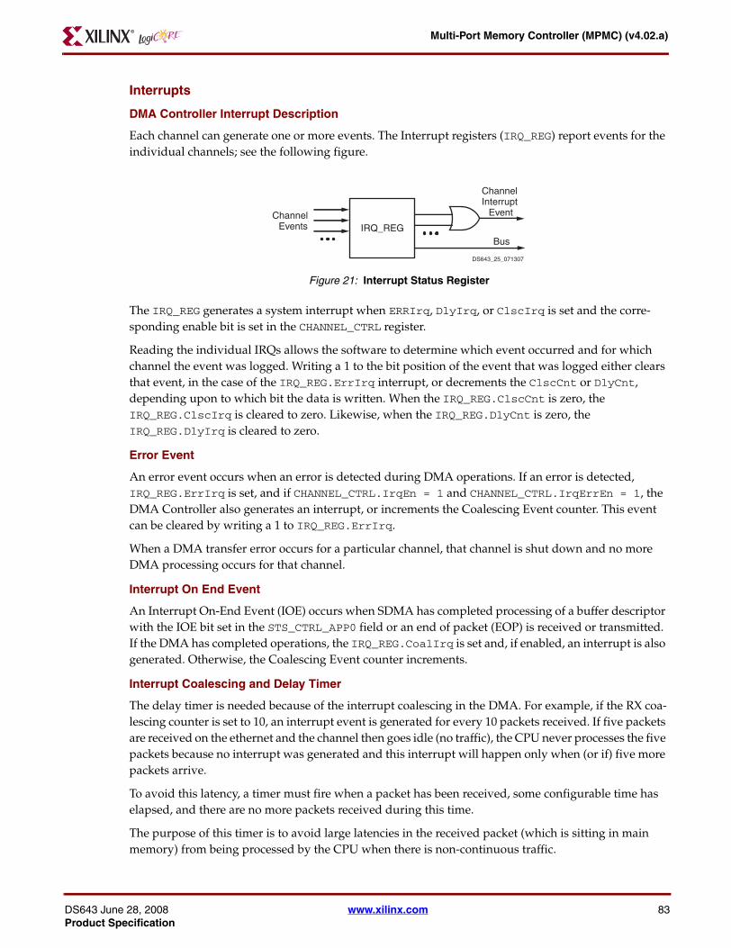
Multi-Port Memory Controller (MPMC) (v4.02.a)
DS643 JuneProduct Sp
Interrupts
DMA Controller Interrupt Description
Each channel can generate one or more events. The Interrupt registers (IRQ_REG) report events for the individual channels; see the following figure.
The IRQ_REG generates a system interrupt when ERRIrq, DlyIrq, or ClscIrq is set and the corre-sponding enable bit is set in the CHANNEL_CTRL register.
Reading the individual IRQs allows the software to determine which event occurred and for which channel the event was logged. Writing a 1 to the bit position of the event that was logged either clears that event, in the case of the IRQ_REG.ErrIrq interrupt, or decrements the ClscCnt or DlyCnt, depending upon to which bit the data is written. When the IRQ_REG.ClscCnt is zero, the IRQ_REG.ClscIrq is cleared to zero. Likewise, when the IRQ_REG.DlyCnt is zero, the IRQ_REG.DlyIrq is cleared to zero.
Error Event
An error event occurs when an error is detected during DMA operations. If an error is detected, IRQ_REG.ErrIrq is set, and if CHANNEL_CTRL.IrqEn = 1 and CHANNEL_CTRL.IrqErrEn = 1, the DMA Controller also generates an interrupt, or increments the Coalescing Event counter. This event can be cleared by writing a 1 to IRQ_REG.ErrIrq.
When a DMA transfer error occurs for a particular channel, that channel is shut down and no more DMA processing occurs for that channel.
Interrupt On End Event
An Interrupt On-End Event (IOE) occurs when SDMA has completed processing of a buffer descriptor with the IOE bit set in the STS_CTRL_APP0 field or an end of packet (EOP) is received or transmitted. If the DMA has completed operations, the IRQ_REG.CoalIrq is set and, if enabled, an interrupt is also generated. Otherwise, the Coalescing Event counter increments.
Interrupt Coalescing and Delay Timer
The delay timer is needed because of the interrupt coalescing in the DMA. For example, if the RX coa-lescing counter is set to 10, an interrupt event is generated for every 10 packets received. If five packets are received on the ethernet and the channel then goes idle (no traffic), the CPU never processes the five packets because no interrupt was generated and this interrupt will happen only when (or if) five more packets arrive.
To avoid this latency, a timer must fire when a packet has been received, some configurable time has elapsed, and there are no more packets received during this time.
The purpose of this timer is to avoid large latencies in the received packet (which is sitting in main memory) from being processed by the CPU when there is non-continuous traffic.
Figure Top x-ref 20
Figure 21: Interrupt Status Register
IRQ_REGBus
ChannelEvents
Channel Interrupt
Event
DS643_25_071307
28, 2008 www.xilinx.com 83ecification

Multi-Port Memory Controller (MPMC) (v4.02.a)
As shown in the following figure, the Clock Divider module uses a 10-bit value, C_PRESCALAR, to determine how many LocalLink clock cycles to count before generating a single Timer_ce pulse. For a typical LocalLink clock speed of 200MHz and C_PRESCALAR=1023, this translates to a 5.12 usec Timer_ce period. Therefore, the 8-bit timer is able to count up to a maximum of 256*5.12 = 1.3 msecs, before generating an interrupt.
Note: When the Coalescing Counter fires, the delay timer automatically clears.
The Interrupt Coalescing counter is an additional mechanism for interrupt handing. It can relieve the need for the CPU to service an interrupt at the end of every packet. Instead, a pre-loadable number of interrupt events (up to 256) generate a single interrupt to the CPU. The following figure shows the mechanism used for the Tx coalescing counter interrupt generation.
Figure 22: Delay Timer Interrupt Scheme
Figure 23: Coalescing Counter Interrupt Scheme
ClockDivider
Timer_ce
Timer_int=
Timer_ce_maskTimer_rst: set to 0Link_EOF: sets to 1
Timer_intOR
(IRQ_REG.CoalIrq AND CHNL_CTRLIrqCoalEn)OR
LinkSOFOR
Channel_ResetOR
CHNL_CTRL.IRQTimout=0 CH
NL_
CT
RL.
IRQ
Tim
eout
IRQ
_RE
G.D
lyT
mrV
alue
LLink_Clk
DS643_26_071307
RST
CE
IRQ
_RE
G.D
lyT
mrV
aluelncr
Decr
IRQ_REQ_WE AND IRQ_REG.DlyIRQ
Coal_int= 0
[(Link_EOF And not (CHNL_CTRLUseIntOnEnd)OR
(STS_CTRL_APP0.IntOnEnd AND CHNL_CTRL.UseIntOnEnd)]AND
Descriptor_UpdatedAND
PI_WrFIFO_Empty
CHNL_CTRL.IRQCount
IRQ
_RE
G.C
lscC
ntrV
alue
DS643_27_071307
Load
D
IRQ
_RE
G.C
oalC
nt
Decr
IncrDecr
Coal_int0
IRQ_REQ_WE AND IRQ_REG.CoaIRQ
CHNL_CTRLLdrIRQCntOR
(Timer_Int AND CHNL_CTRIrqDlyEn)OR
Coal_Int
84 www.xilinx.com DS643 June 28, 2008Product Specification

Multi-Port Memory Controller (MPMC) (v4.02.a)
DS643 JuneProduct Sp
In this example:
• Upon reset, the CHNL_CTRL.IRQC count value is used to load the Coalescing Counter. Subsequently, the register field, TxIrqCountReg[0:7], can be programmed with any 8-bit value.
• On every EOP or irq-on-end (selected by CHNL_CTRL_UseIntOnEnd), the counter will decrement. When the Coalescing Counter hits 0, the DMA increments the 4-bit Interrupt Counter.
• When the 4-bit int counter is non-zero, it generates an interrupt to the CPU (if the irq_enable bit of the respective channel is set).
• When the interrupt is acknowledged (with a DCR write value of 1), the 4-bit Interrupt Counter is decremented.
• The contents of the TxIrqCountReg[0:7] register is reloaded when the 4-bit Interrupt Counter increments.
There is also a means provided for the CPU to force the counter to load the contents of the TxIrqCountReg[0:7] register. This is achieved when the CPU writes the ldIrqCnt field.
Note: When the delay timer fires, the Coalescing Counter automatically reloads.
DMA Engine Reset
A capability is included to reset a particular DMA engine (both RX and TX channels simultaneously) whenever a “lockup” situation arises or an error is detected.
The software reset bit, DMA_CONTROL_REG.SwReset allows the software application to reset SDMA. When you write a 1 to DMA_CONTROL_REG.SwReset, it initiates the reset sequence for that SDMA. At the same time, the SDMA_RstOut output is asserted, synchronous to the LocalLink clock. This output can be used as an external logic reset.
After a soft reset is initiated, software needs to poll the DMA_CONTROL_REG.SwReset bit until it is sam-pled as de-asserted. This indicates that the reset sequence has completed and the pipeline is flushed. Simultaneously with the DMA_CONTROL_REG.SwReset bit being cleared, the SDMA_RstOut is automat-ically de-asserted.
Note: When the DMA engine reset function is used, there is no guarantee that the current descriptor completed correctly. The assumption should be that the descriptor did not complete and it should be restarted again using the normal CPU technique for starting a new DMA operation.
Transaction Timing
The following subsections describe transaction timing for SDMA.
Descriptor Fetch
The following figure shows NPI port interface timing for a descriptor fetch. The SDMA uses 8-word, cacheline reads to perform a descriptor fetch. The timing from when the SDMA makes a request of the NPI will depend on arbitration in MPMC. The SDMA monitors PI_RdFIFO_Empty to determine when to begin to pop data out of the MPMC read FIFO.
28, 2008 www.xilinx.com 85ecification

Multi-Port Memory Controller (MPMC) (v4.02.a)
86
Descriptor Update
The following figure shows the MPMC port interface timing for a descriptor fetch. The SDMA uses 8-word cacheline writes to perform a descriptor update. The SDMA will push the data into the MPMC write FIFO if there is space available. After the data has been pushed to the FIFO, the SDMA makes a write request to the MPMC.
Figure Top x-ref 21
Figure 24: Descriptor Fetch Timing
Figure Top x-ref 22
Figure 25: Descriptor Update Timing
PI_ClkPI_Addr[31:0]
PI_AddrReqPI_RNW
PI_AddrAckPI_Size[3:0]
PI_RdFIFO_Data[63:0]PI_RdFIFO_Pop
PI_RdFIFO_RdWdAddr[3:0]PI_RdFIFO_EmptyPI_RdFIFO_Flush
PI_WrFIFO_Data[63:0]PI_WrFIFO_BE[7:0]
PI_WrFIFO_PushPI_WrFIFO_AlmostFull
PI_WrFIFO_Flush
2
A0
D0 D1 D2 D3
2 4 6 8
Time from PI_Addr Req to Read Data Available will vary
DS643_28_071307
0ns 20ns 40ns 60ns 80ns 100ns 120ns 140ns
0ns 20ns 40ns 60ns 80ns 100nsPI_Clk
PI_Addr[31:0]PI_AddrReq
PI_RNWPI_AddrAckPI_Size[3:0]
PI_RdFIFO_Data[63:0]PI_RdFIFO_Pop
PI_RdFIFO_RdWdAddr[3:0]PI_RdFIFO_DataAvailable
PI_RdFIFO_EmptyPI_RdFIFO_Flush
PI_WrFIFO_Data[63:0]PI_WrFIFO_BE[7:0]
PI_WrFIFO_PushPI_WrFIFO_AlmostFull
PI_WrFIFO_Flush
2 4 6 8
2
D0 D1 D2 D3
FF FF FF FF
A0
DS643_29_071307
www.xilinx.com DS643 June 28, 2008Product Specification

Multi-Port Memory Controller (MPMC) (v4.02.a)
DS643 JuneProduct Sp
Transmit Data Read
The following figure shows a transmit data read (fetch) from the MPMC. The SDMA uses 32-word (or 16-double word) reads to fetch data for transmitting across LocalLink. Reads always begin at 32-word boundaries. The SDMA uses the data starting with the current buffer address only; additional invalid data fetched due to the 32-word boundary restriction is ignored.
Receive Data Write
The following figure shows received data being written to the MPMC. The SDMA uses 32-word burst writes to write data to MPMC. The transfers are always 32-word aligned. The PI_WrFIFO_BE bus is used to indicate which bytes of the 32 words are valid. The first two bytes are shown as being invalid and the last byte is also invalid.
Figure Top x-ref 23
Figure 26: Transmit Data Read
Figure Top x-ref 24
Figure 27: Receive Data Write
0ns 50ns 100ns 150ns 200ns 300ns250ns 350ns
Time from PI_Addr Req to Read Data Available will vary
PI_ClkPI_Addr[31:0]
PI_AddrReqPI_RNW
PI_AddrAckPI_Size[3:0]
PI_RdFIFO_Data[63:0]PI_RdFIFO_Pop
PI_RdFIFO_RdWdAddr[3:0]PI_RdFIFO_EmptyPI_RdFIFO_Flush
PI_WrFIFO_Data[63:0]PI_WrFIFO_BE[7:0]
PI_WrFIFO_PushPI_WrFIFO_AlmostFull
PI_WrFIFO_Flush
4
0
D0 D1 D2 D3 D4 D5 D6 D7 D12 D13 D14 D15D8 D9 D10 D11
A0
DS643_30_071307
PI_CIk
0ns 50ns 100ns 150ns 250ns200ns 300ns
PI_Addr[31:0]
PI_Size[3:0]
PI_AddrReq
PI_AddrAck
PI_RdFIFO_Data[63:0]
PI_WrFIFO_Data[63:0]
PI_WrFIFO_BE[7:0]
PI_WrFIFO_Push
PI_WrFIFO_AlmostFull
PI_WrFIFO_Flush
PI_RdFIFO_DataAvailable
PI_RdFIFO_Empty
PI_RdFIFO_Flush
PI_RdFIFO_RdWdAdd[3:0]
PI_RdFIFO_Pop
PI_RNW
A0
4
FFFFFFFFFFFFFFFFFFFF3F FFFFFFFF FE
D15D14D13D12D11D10D9D8D7D6D5D4D3D2D1D0
DS607_24_030408
28, 2008 www.xilinx.com 87ecification
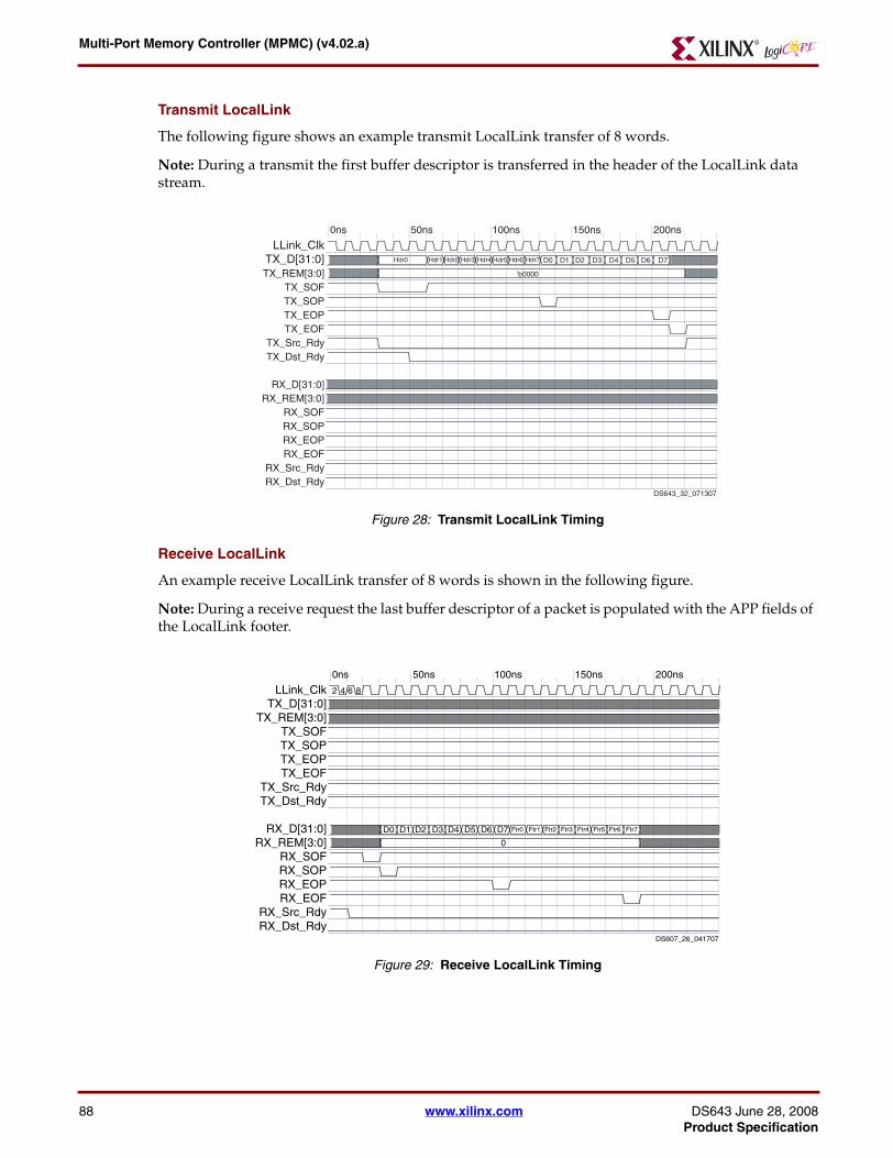
Multi-Port Memory Controller (MPMC) (v4.02.a)
88
Transmit LocalLink
The following figure shows an example transmit LocalLink transfer of 8 words.
Note: During a transmit the first buffer descriptor is transferred in the header of the LocalLink data stream.
Receive LocalLink
An example receive LocalLink transfer of 8 words is shown in the following figure.
Note: During a receive request the last buffer descriptor of a packet is populated with the APP fields of the LocalLink footer.
Figure Top x-ref 25
Figure 28: Transmit LocalLink Timing
Figure Top x-ref 26
Figure 29: Receive LocalLink Timing
0ns 50ns 100ns 150ns 200ns
LLink_ClkTX_D[31:0]TX_REM[3:0]
TX_SOFTX_SOPTX_EOPTX_EOF
TX_Src_RdyTX_Dst_Rdy
RX_D[31:0]RX_REM[3:0]
RX_SOFRX_SOPRX_EOPRX_EOF
RX_Src_RdyRX_Dst_Rdy
'b0000
Hdr7Hdr1Hdr0 Hdr2 Hdr3 Hdr4 Hdr5 Hdr6 D0 D1 D2 D3 D4 D5 D6 D7
DS643_32_071307
0ns 50ns 100ns 150ns 200ns
LLink_ClkTX_D[31:0]
TX_REM[3:0]TX_SOFTX_SOPTX_EOPTX_EOF
TX_Src_RdyTX_Dst_Rdy
RX_D[31:0]RX_REM[3:0]
RX_SOFRX_SOPRX_EOPRX_EOF
RX_Src_RdyRX_Dst_Rdy
2 4 6 8
Ftr7Ftr1Ftr0 Ftr2 Ftr3 Ftr4 Ftr5 Ftr6D0 D1 D2 D3 D4 D5 D6
0
D7
DS607_26_041707
www.xilinx.com DS643 June 28, 2008Product Specification

Multi-Port Memory Controller (MPMC) (v4.02.a)
DS643 JuneProduct Sp
SDMA Registers
The SDMA registers are detailed in the following subsections.
Next Descriptor Pointer (TX_NXTDESC_PTR and RX_NXT_DESC_PTR) Offsets: 0x00 and 0x20
The Next Descriptor Pointers TX_NXTDESC_PTR (Transmit) and RX_NXT_DESC_PTR (Receive), are loaded from the Next Descriptor Pointer field in the current descriptor for the respective channel. This value is kept in the respective SDMA register until the SDMA has completed all DMA transactions within the DMA transfer.
After DMA transactions are complete, the current descriptor is complete and the SDMA_COMPLETED bit is set in the respective status register. The current descriptor is written to update the status of the STS_CTRL_APP0 field within the descriptor.
Then the SDMA evaluates if there is a halt condition that occurs when the Current Descriptor Pointer equals the Tail Descriptor Pointer. If there is no halt condition, the address contained in the Next Descriptor Pointer register is evaluated as follows:
• If a NULL (0x00000000) is contained in the Next Descriptor Pointer register, the SDMA engine stops processing buffer descriptors.
• If the address contained in the Next Descriptor Pointer register is not 8-word aligned or reaches beyond the range of available memory, the SDMA halts processing and sets the SDMA_ERROR bit in the respective status register (TX_CHNL_STATUS or RX_CHNL_STATUS).
• If the Next Descriptor Pointer register contains a valid address, the contents are moved to the respective Current Descriptor Register (TX_CURDESC_PTR or RX_CUR_DESC_PTR).
Then the SDMA begins another DMA transaction. The following table describes the Next Description Pointer (TX_ and RX_) register bits.
Table 37: Next Descriptor Pointer Register Description
Bit(s) NameCore
AccessReset Value
Description
0:31TX_NXTDESC_PTR and RX_NXT_DESC_PTR
Read 0x00000000
8 word aligned pointer to the next buffer descriptor in the chain. If NULL (0x00000000), DMA engine stops processing buffer descriptors.
28, 2008 www.xilinx.com 89ecification
Multi-Port Memory Controller (MPMC) (v4.02.a)
90
Current Buffer Address (TX_CURBUF_ADDR and RX_CURBUF_ADDR) Offsets: 0x04 and 0x24
The Current Buffer Address register, one for transmit and one for receive, maintains the contents of the address in memory where the DMA operation is conducted next. This value is originally loaded into the SDMA when the descriptor is read by the SDMA.
When set by the current buffer descriptor, the SDMA periodically transfers this value to an internal Address Counter that then updates the value for each DMA transaction completed.
Upon termination of the transaction, the SDMA overwrites the value of the Current Buffer Address register with the last value of the Address Counter.
This process continues repeatedly until the SDMA has completed the current descriptor. The reason for this mechanism is so the SDMA can maintain multiple temporal channels of DMA at a substantially reduced hardware cost. It is not recommended that software use the Current Buffer Address register to determine SDMA progress because it changes dynamically. The following table describes the Current Buffer Address register bits.
Current Buffer Length (TX_CURBUF_LENGTH, RX_CURBUF_LENGTH) Offsets:0x08 and 0x28
The Current Buffer Length register, one for transmit and one for receive, maintains the contents of the remaining length of the data to be transferred by the SDMA. The value is originally loaded into the SDMA when the descriptor is read by the SDMA. When set by the current descriptor, the SDMA peri-odically transfers this value to an Internal Length Counter, which then updates the value for each DMA transaction completed.
Upon termination of the transaction, the SDMA overwrites the value of the Current Buffer Length reg-ister with the last value of the internal length counter. This process continues repeatedly until the SDMA has completed the current descriptor. The following table describes the Current Buffer Length register bits.
Table 38: Current Buffer Address Register Description
Bit(s) NameCore
AccessReset Value
Description
0:31TX_CURBUF_ADDR and RX_CUR_BUF_ADDR
Read 0x00000000Address to the current buffer being processed by SDMA.
Table 39: Current Buffer Length Register Description
Bit(s) NameCore
AccessReset Value
Description
0:31TX_CURBUF_LENGTHand RX_CURBUF_LENGTH
Read 0x00000000Length in bytes of the current buffer being processed by SDMA.
www.xilinx.com DS643 June 28, 2008Product Specification

Multi-Port Memory Controller (MPMC) (v4.02.a)
DS643 JuneProduct Sp
Current Descriptor Pointer (TX_CURDESC_PTR, RX_CURDESC_PTR) Offsets: 0x0C and 0x2C
The Current Descriptor Pointer register, one for transmit and one for receive, maintains the pointer to the buffer descriptor that is currently being processed. The value was set either by the CPU when it first initiated a DMA operation, or is copied from the Next Descriptor Pointer register upon completion of the prior descriptor. This value is maintained by the SDMA as a pointer so that the SDMA can update the Status and Application Dependent fields of the descriptor after the buffer descriptor has been fully processed. The following table describes the Current Descriptor Pointer register bits.
Tail Descriptor Pointer (TX_TAILDESC_PTR and RX_TAILDESC_PTR) Offsets: 0x10 and 0x30
The Tail Descriptor Pointer register, one for transmit and one for receive, maintains the pointer to the buffer descriptor chain tail. Tail Pointer Mode is always enabled; consequently, DMA operations will halt when processing of the buffer descriptor pointed to by TAILDESC_PTR is completed. Writing to this register will start DMA operations. The following table describes the Tail Descriptor Pointer regis-ter bits.
Table 40: Current Descriptor Pointer Register Description
Bit(s) NameCore
AccessReset Value
Description
0:31TX_CURDESC_PTR and RX_CURDESC_PTR
Read/Write 0x00000000An 8-word aligned pointer to the current buffer descriptor being processed by the SDMA.
Table 41: Tail Descriptor Pointer Register Description
Bit(s) NameCore
AccessReset Value
Description
0:31TX_TAILDESC_PTR and RX_TAILDESC_PTR
Read/Write 0x00000000An 8-word aligned pointer to the tail descriptor. The software application writes to this field to initiate a DMA transfer.
28, 2008 www.xilinx.com 91ecification

Multi-Port Memory Controller (MPMC) (v4.02.a)
92
Channel Control Register (TX_CHNL_CTRL and RX_CHNL_CTRL) Offsets: 0x14 and 0x34
The Channel Control register, one for transmit and one for receive, controls interrupt processing for the particular channel. The following figure illustrates the Channel Control register, and the table below the figure describes the Channel Control register bits.
Figure Top x-ref 27
Figure 30: Channel Control Register
Table 42: Channel Control Register
Bit(s) NameCore
AccessReset Value
Description
0:7 IRQTimeout Read/Write 0
Interrupt Delay Time-out ValueThe maximum amount of time that an unreported packet is required to wait until generating a Delay Interrupt (DlyIRQ) event. (Must remain unchanged for the duration of an DMA operation.)
8:15 IRQCount Read/Write FF
Interrupt Coalescing Threshold Count ValueThe number of packets that must be received to generate a Coalescing Interrupt (ClscIrq) event. This value is loaded into the packet threshold counter when LdIrqCnt = 1 and subsequently re-loaded whenever the threshold count is reached.
16:20 Reserved Reserved - Read as zero.
21 Use1BitCnt Read/Write 0 Use 1 Bit Wide Counters. Currently Not Used.
22 UseIntOnEnd Read/Write 0
Use Interrupt On End: Selects between using the interrupt-on-end mechanism or using the EOP mechanism for interrupt coalescing.1 - Selects the interrupt-on-end mechanism0 - Selects the EOP mechanism
23 LdIRQCnt Write 0
Load IRQ Count:Writing a 1 to this field forces the loading of the Interrupt Coalescing counters from the CHANNEL_CTRL.IrqCount[0:7] field. This is a self-clearing field. Read as zero
24 IrqEn Read/Write 0Master Interrupt Enable: When set, indicates that the DMA channel is enabled to generate interrupts. This is the master enable for the channel. Individual sources can be enabled and disabled separately.
25:28 Reserved Reserved - Read as zero
29 IrqErrEn Read/Write 0Interrupt on Error Enable: When set, indicates that an interrupt will be generated if an error occurs
30 IrqDlyEn Read/Write 0Interrupt on Delay Enable: When set, indicates that an interrupt will be generated when the time-out value is reached.
31 IrqCoalEn Read/Write 0Interrupt on Count Enable: When set, indicates that an interrupt will be generated when the interrupt coalescing threshold value is reached.
0
DS643_14_071307
ReservedReserved IrqCoalEnIrqErrEn
LdlRQCntIrqErrEn
IrqDlyEnIRQCountIRQTimeout IrqEnUseIntOnEnd
7 8 15 16 20 21 22 23 24 25 28 29 30 31
www.xilinx.com DS643 June 28, 2008Product Specification

Multi-Port Memory Controller (MPMC) (v4.02.a)
DS643 JuneProduct Sp
Interrupt Status Register (TX_IRQ_REG and RX_IRQ_REG) Offsets: 0x18 and 0x38
The Interrupt Status register, one for transmit and one for receive, indicates interrupt pending and interrupt coalescing count values. This register is used by the software application also to acknowledge pending interrupts by writing a 1 to clear the pending interrupts. The following figure illustrates the Interrupt Status register, and the table that follows describes the Interrupt Status register bits.
Figure Top x-ref 28
Figure 31: Interrupt Status Register
Table 43: Interrupt Status Register
Bit(s) NameCore
AccessReset Value
Description
0:7 DlyTmrValue Read 0Delay Timer Value This field contains the real time delay timer value.
8:15 ClscCntrValue Read FFCoalesce Counter Value This field contains the real time coalesce counter value.
16:17 Reserved Reserved - read as zero.
18:21 ClscCnt Read 0Coalesce Interrupt Count Indicates the number of events due to reaching the interrupt coalesce threshold.
22:23 DlyCnt Read 0Delay Interrupt Count Indicates the number of events due to reaching the wait bound delay time.
24:28 Reserved Reserved - read as zero
29 ErrIrq Read/Write 0Error Interrupt EventIndicates that an error has occurred. Writing a 1 to this bit clears the interrupt.
30 DlyIrq Read/Write 0Delay Interrupt Event Indicates that delay time-out event has occurred. Writing a 1 to this bit clears the interrupt.
31 Coallrq Read/Write 0Coalesce Interrupt Event. Indicates that an interrupt event threshold count has been reached. Writing a 1 to this bit clears the interrupt.
0
DS643_15_071307
ReservedReserved CoalIrq
DlyIrq
DlyCnt ErrIrq
ClscCntValueDlyTmrValue ClscCnt
7 8 15 16 20 21 22 23 24 28 29 30 3117 18 19
28, 2008 www.xilinx.com 93ecification

Multi-Port Memory Controller (MPMC) (v4.02.a)
94
Channel Status Register (TX_CHNL_STS and RX_CHNL_STS) Offsets: 0x1C and 0x3C
The Channel Status register, one for transmit and one for receive, contains status for a particular chan-nel. The following figure illustrates the Channel Status register, and the table that follows describes the Channel Status register bits.
Figure Top x-ref 29
Figure 32: Channel Status Register
Table 44: Channel Status Register
Bit(s) NameCore
AccessReset Value
Description
0:9 Reserved Reserved - Read as zero
10 TailPErr Read 0Tail Pointer Error: This bit indicates that Tail Pointer is NOT a valid address. Valid addresses are between C_PI_BASEADDR and C_PI_HIGHADDR.
11 CmpErr Read 0
Complete Error: This bit indicates a descriptor was fetched with the Cmplt = 1 in the STS_CNTRL_APP0 field of the descriptor. This error check is enabled by setting C_COMPLETED_ERR_RX and/or C_COMPLETED_ERR_TX to 1 for the respective channel.
12 AddrErr Read 0Address Error: This bit indicates the Current Buffer Address is NOT a valid address. Valid addresses are between C_PI_BASEADDR and C_PI_HIGHADDR.
13 NxtPErr Read 0Next Descriptor Pointer Error: This bit indicates the Next Descriptor Pointer is NOT a valid address. Valid addresses are between C_PI_BASEADDR and C_PI_HIGHADDR.
14 CurPErr Read 0Current Descriptor Pointer Error: This bit indicates the Current Descriptor Pointer is NOT a valid address.Valid addresses are between C_PI_BASEADDR and C_PI_HIGHADDR.
15 BsyWr Read 0Busy Write Error: This bit indicates the Current Descriptor Pointer register was written to while the DMA Engine was busy.
16:23 Reserved Reserved - Read as zero
24 Error Read 0DMA Error: This bit indicates that an error occurred during DMA operations. This bit is an OR’ing of error bits 10 to 15.
25 IOE Read 0Interrupt On End: This bit is a copy of the corresponding bit in the STS_CTRL_APP0 field of the descriptor.
26 SOE Read 0Stop On End: This bit is a copy of the corresponding bit in the STS_CTRL_APP0 field of the descriptor.
27 Cmplt Read 0Complete: When set indicates that the DMA has transferred all data defined by the current descriptor.
0
DS643_16_080307
ReservedReserved Rsvd
EngBusySOPSOEErrorAddrErrTailErr CurPErr
EOPIOE CmpltBsyWrNxtPErr
CmpErr
15 16 23 24 28 29 30 319 10 11 12 13 14 25 26 27
www.xilinx.com DS643 June 28, 2008Product Specification

Multi-Port Memory Controller (MPMC) (v4.02.a)
DS643 JuneProduct Sp
DMA Control Register (Offset: 0x40)
The DMA Control register controls the DMA operation. The following figure illustrates the DMA Con-trol register, and the table that follows describes the DMA Control register bits.
28 SOP Read 0
Start of Packet (SOP): When set indicates that the current descriptor is the start of a packet. For transmit, the CPU sets this bit in the descriptor to indicate that this is the first descriptor of a packet to be transmitted. For receive, when an SOP is received by the LocalLink interface, the DMA sets this bit in the descriptor. This informs the CPU that this descriptor is the first descriptor of the packet.
29 EOP Read 0
End of Packet (EOP): When set, indicates that the current descriptor is the final one of a packet. For transmit the CPU sets this bit in the descriptor to indicate that this is the last descriptor of a packet to be transmitted. For receive, when a EOP is received by LocalLink interface, the DMA sets this bit in the descriptor. This informs the CPU that the current descriptor is the first of a received packet.
30 EngBusy Read 0
Engine Busy: When set, indicates that the respective channel is busy with a DMA operation. Generally, software should not write any DMA registers while this bit is set. Reading of registers is allowed.
31 Reserved Read Reserved - Read as zero
Figure Top x-ref 30
Figure 33: DMA Control Register
Table 45: DMA Control Register
Bit(s) NameCore
AccessReset Value
Description
0:26 Reserved 0 Reserved - read as zero
27 Reserved 1 Reserved - read as one
28 Reserved 1 Reserved - read as one
29 Reserved 1 Reserved - read as one
30 Reserved 0 Reserved - read as zero
31 SwReset Read/Write 0
Software Reset Writing a 1 to this field forces the DMA engine to shutdown and reset itself. After setting this bit, software must poll it until the bit is cleared by the DMA. This indicates that the reset process is done and the pipeline has been flushed1= Reset DMA - Resets both Rx and Tx Channels0= Normal Operation (default)
Table 44: Channel Status Register (Continued)
Bit(s) NameCore
AccessReset Value
Description
0
DS643_17_071307
Reserved SwReset
Rsvd
‘1’
‘1’
‘1’
28 29 30 3126 27
28, 2008 www.xilinx.com 95ecification

Multi-Port Memory Controller (MPMC) (v4.02.a)
Processor Local Bus Version 4.6 PIM
The Processor Local Bus version 4.6 (PLB v4.6) PIM provides the interconnect from the PLB v4.6 bus to the MPMC.
PLB v4.6 PIM Features
The PLB v4.6 PIM supports the following features:
• IBM CoreConnect™ 32-, 64-, and 128-bit PLB compatibility conforming to PLB v4.6 with Xilinx simplifications. See "Reference Documents" page 163 for links to more information.
• Access by 32-, 64-, and 128-bit masters. The PLB data and address signals are labelled with big-endian bit and byte ordering as described in Figure 8 on page 56.
• Single, data-beat read and write data transfers
• Fixed-burst read and write data transfers
• 4- and 8-word, cacheline read and write transfers
• PLB Point-to-Point (P2P) configuration
• Supports 1:1 and 2:1 (MPMC:PIM) synchronous clock ratios (automatically detected during reset)
• PIM<Port_Num>_PLB_SAValid on PLB read transfers to minimize bubbles between reads
• 32-bit address offset (the optional address offset is added to the PLB transaction address to compute the physical memory address to be accessed)
PLB v4.6 PIM Overview
PLB v4.6 PIM provides the interconnect from the PLB v4.6 bus to the MPMC.
Over NPI, PLB v4.6 PIM translates a PLB transaction into one or more NPI transactions. These NPI transactions can be byte, half-word, word, 4- and 8-word, cacheline transactions. The NPI transactions type can be 16 word bursts or 32 word bursts also, depending on the value of C_SPLB<Port_Num>_NATIVE_DWIDTH.
If the generic C_SPLB<Port_Num>_NATIVE_DWIDTH is set to 64, the PIM requests 32 word NPI bursts from MPMC; however, if C_SPLB<Port_Num>_NATIVE_DWIDTH is set to 32, the PIM will request 16 word NPI bursts from MPMC. The PLB v4.6 PIM translates PLB transactions into these discrete NPI transactions. Because PLB bursts can have a fixed length ranging from 1 to 16 data beats and can start at different addresses, the PIM must arrange PLB data to fit the available set of NPI transaction types.
The PLB v4.6 PIM is configured by the XPS to various subtypes based on the port to which the PIM is connected. The SUBTYPEs are DPLB, IPLB, Single, and PLB:
• The DPLB SUBTYPE is chosen when the PIM is connected to a PowerPC 405 processor DPLB1 port using a point-to-point connection.
• The IPLB SUBTYPE is chosen when the PIM is connected to a PowerPC 405 processor IPLB1 port using a point-to-point connection. When this sub type is chosen, the write FIFO logic in the MPMC data path is also disabled (C_PI<Port_Num>_WR_FIFO_TYPE = DISABLED).
• The Single SUBTYPE is chosen when the PIM is connected to a PLB bus where all masters are not burst capable. This is primarily selected in MicroBlaze systems where the PIM is connected to a bus with MicroBlaze IPLB and DPLB ports.
• The PLB SUBTYPE is chosen in all other cases. This PLB PIM supports the full set of PLB transactions.
You can find information regarding the PIM SUBTYPES in “Configuring PLB v4.6 PIM SUBTYPES,” page 98.
96 www.xilinx.com DS643 June 28, 2008Product Specification

Multi-Port Memory Controller (MPMC) (v4.02.a)
Supported NPI Transfer Types
Based on the setting of C_SPLB<Port_Num>_NATIVE_DWIDTH, the PLB v4.6 PIM can generate only certain types of NPI transfers, as shown in the following table.
Supported PLB Master and Bus WidthsThe following table indicates that a 64-bit NATIVE_DWIDTH PLB PIM can talk to 32-, 64-, or 128-bit masters. A 32 bit NATIVE_DWIDTH PIM can only be used with a PLB bus where all masters and slaves on the bus are 32 bits only. The 32-bit NATIVE_DWIDTH PIM is intended for Spartan-3 based systems.
To reduce the number of cycles between read transactions, the PLB v4.6 PIM can accept PLB read transactions when SPLB<Port_Num>_PLB_SAValid is asserted. This allows a subsequent MPMC request to be asserted after the current request has been acknowledged.
Table 46: Supported Transactions based on PIM Subtype and Native Width
C_SPLB<Port_Num>_NATIVE_DWIDTH=32 C_SPLB<Port_Num>_NATIVE_DWIDTH=64
Transaction Type
C_PIM<Port_Num>_SUBTYPE
Transaction Type
C_PIM<Port_Num>_SUBTYPE
PLB DPLB IPLB Single PLB DPLB (1) IPLB(1) Single
Supported Supported
Single Read Y N N Y
Single Read Y Y N Y
Write Y N N Y Write Y Y N Y
4-wd CachelineRead Y N N N
4-wd CachelineRead Y N Y N
Write Y N N N Write Y N N N
8-wd CachelineRead Y N N N
8-wd CachelineRead Y Y Y N
Write Y N N N Write Y Y N N
16-wd BurstRead Y N N N
16-wd BurstRead N N N N
Write Y N N N Write N N N N
32-wd BurstRead N N N N
32-wd BurstRead Y N N N
Write N N N N Write Y N N N
1. Point-to-point configuration is required for the DPLB and IPLB subtypes where the C_SPLB<Port_Num>_NATIVE_DWIDTH=64.
Table 47: Supported PLB Master and Bus Widths
C_SPLB<Port_Num>_NATIVE_DWIDTH=64 C_SPLB<Port_Num>_NATIVE_DWIDTH=32
C_SPLB<Port_Num>_DWIDTHC_SPLB<Port_Num>_SMALLEST_MASTER
SupportedC_SPLB<Port_Num>_DWIDTH
C_SPLB<Port_Num>_SMALLEST_MASTER
Supported
128 128 Y 128 128 N
128 64 Y 128 64 N
128 32 Y 128 32 N
64 64 Y 64 64 N
64 32 Y 64 32 N
32 32 N 32 32 Y
97 www.xilinx.com DS643 June 28, 2008Product Specification

Multi-Port Memory Controller (MPMC) (v4.02.a)
98
Configuring PLB v4.6 for Point-To-Point or Shared Bus
The PLB v4.6 PIM can be configured as either a Point-To-Point (P2P) configuration in which there is only one PLB master communication with the PLB v4.6 PIM or a Shared Bus configuration:
• In P2P configuration, the PLB v4.6 PIM responds to all addresses regardless of the C_PIM<Port_Num>_HIGHADDR and C_PIM<Port_Num>_BASEADDR parameter values. The PLB address is decoded when the PLB v4.6 PIM is operating in a shared bus configuration only.
• In the Shared Bus configuration, the PLB v4.6 PIM can transfer data from up to 16 masters to MPMC. An extra cycle of latency is incurred when the PLB v4.6 PIM operates on a shared bus because PLB signals to the PLB v4.6 PIM are registered to improve timing.
During memory initialization and calibration, the PIM will assert SPLB<Port_Num>_Sl_Wait or SPLB<Port_Num>_Sl_Rearbitrate to hold off any PLB transactions until the memory is ready to process transactions.
Configuring PLB v4.6 PIM SUBTYPES
You can configure the PLB v4.6 PIM with various SUBTYPEs to optimize it for a set of supported trans-actions. In most cases the tools will choose the appropriate PLB v4.6 PIM SUBTYPE automatically, based on the connectivity of the system. The PLB v4.6 PIM SUBTYPEs are:
• 64-Bit Burst PIM
- Single word read and write transactions
- 4-word and 8-word, cacheline read and write transactions
- Fixed length burst transactions
• 32-Bit Burst PIM
- Single word read and write transactions
- 4-word and 8-word, cacheline read and write transactions
- Fixed length burst transactions
• 64-Bit Single PIM
- Single word read and write transactions (reduced size when burst support is not needed)
• 32-Bit Single PIM
- Single word read and write transactions (reduced size when burst support is not needed)
• DPLB
- Single word read and write transactions; and 8-word, cacheline read and write transactions
• IPLB
- 4-word and 8-word, cacheline read transactions
Caution! When choosing a SUBTYPE, be sure the SUBTYPE supports all PLB transaction types that will be issued to the PLBv4.6 PIM. When an unsupported transaction is issued on the PLB bus, it is pos-sible to cause the logic in the PLBv4.6 PIM to hang, requiring a system reset to recover.
www.xilinx.com DS643 June 28, 2008Product Specification

Multi-Port Memory Controller (MPMC) (v4.02.a)
Supported Transactions by SUBTYPE
The supported transactions for each of the SUBTYPES are listed in the following table.
Table 48: Supported Transactions
SPLB_PLB_SIZE (0:3)
SPLB_PLB_SIZE (0:3)
Description Read/WriteC_PIM<Port_Num>_SUBTYPE
PLB DPLB IPLB Single
0x0 Single TransactionsRead Y Y N Y
Write Y Y N Y
0x1 4-wd CachelineRead Y N Y N
Write Y N Y N
0x2 8-wd CachelineRead Y Y Y N
Write Y Y Y N
0x3 16-wd CachelineRead N N N N
Write N N N N
0x4 ReservedRead N N N N
Write N N N N
0x5 ReservedRead N N N N
Write N N N N
0x6 ReservedRead N N N N
Write N N N N
0x7 ReservedRead N N N N
Write N N N N
0x8 Byte BurstsRead N N N N
Write N N N N
0x9 Half Word BurstsRead N N N N
Write N N N N
0xA Word BurstsRead Y N N N
Write Y N N N
0xB Double Word BurstsRead Y N N N
Write Y N N N
0xC Quad Word BurstsRead Y N N N
Write Y N N N
0xD Octal Word BurstsRead N N N N
Write N N N N
0xE ReservedRead N N N N
Write N N N N
0xF ReservedRead N N N N
Write N N N N
SPLB_PLB_TYPE (0:2)
SPLB_PLB_TYPE (0:2)
Description Read/WriteC_PIM<Port_Num>_SUBTYPE
PLB DPLB IPLB Single
000b Memory TransferRead Y Y Y Y
Write Y Y Y Y
001b-111b N/ARead N N N N
Write N N N N
Indeterminate BurstRead N N N N
Write N N N N
Burst request of 2-16 databeatsRead Y N N N
Write Y N N N
Burst request of > 16 databeatsRead N N N N
Write N N N N
99 www.xilinx.com DS643 June 28, 2008Product Specification

Multi-Port Memory Controller (MPMC) (v4.02.a)
100
PowerPC 440 Memory Controller PIM
The PowerPC 440 Memory Controller (PPC440MC) PIM connects MPMC directly to the memory inter-face port of the PowerPC 440 block in Virtex-5 FXT devices.
Note: The ppc440mc_ddr2 IP core should be used instead of MPMC whenever possible. The ppc440mc_ddr2 IP core is optimized as a single port DDR2 memory for the PowerPC440 memory interface. The ppc440mc_ddr2 IP core offers lower latency and higher Fmax than MPMC. MPMC should only be used when SDRAM/DDR memory support or multiple memory ports are needed.
Features• Supports The Virtex-5, V5FXT, memory interface.
• Supports 32-bit and 64-bit NPI interfaces using 32-bit and 64-bit PPC440MC data widths.
• Runs with 1:1 clocking with NPI and MIB.
• Provides parameterized burst sizes of 2, 4, and 8.
• Supports read data latency of 0, 1, and 2 clocks.
• Can operate at a 1:1, 1:2, 1:3, or 1:4 clock ratio with respect to the PowerPC crossbar interconnect clock (CPMINTERCONNECTCLK)
Supported PowerPC 440 Memory Controller Interface Configuration
The PPC440MC PIM requires the following configuration settings in the MI_CONTROL Register of the PowerPC 440 Block.
Table 49: Required PPC440 Block MI_CONTROL Register Settings
Bit(s) NameRequired
Value Setting
Description
[0] enable 1 Turn on the PPC440MC interface.
[1] Rowconflictholdenable 0PPC440MC PIM does not support row/bank management.
[2] Bankconflictholdenable 0PPC440MC PIM does not support row/bank management.
[3] Directionconflictholdenable 0PPC440MC PIM does not support row/bank management.
[4:5] Autoholdduration 00 PPC440MC PIM only supports this autohold mode.
[6] 2:3 Clock Ratio mode 0PPC440MC PIM only supports integer clock ratios. It does not support a clock ratio of 2:3 with respect to CPMINTERCONNECTCLK.
[7] overlaprddwr 0Overlapped transfers and QDR mode are not supported.
[8:9] Burstwidth N/ASee “PPC440MC Parameter and Port Dependencies,” page 102 for supported values.
[10:11] Burstlength N/ASee “PPC440MC Parameter and Port Dependencies,” page 102 for supported values.
[12:15] Write Data Delay (WDD) 0000 PPC440MC PIM supports this WDD mode only.
[16] RMW 0 PPC440MC PIM supports this setting only.
www.xilinx.com DS643 June 28, 2008Product Specification

Multi-Port Memory Controller (MPMC) (v4.02.a)
DS643 JuneProduct Sp
All bits not shown in Table 49 on page 100 can normally be set by the users as described in the “Embed-ded Processor Block” of the Virtex-5 FPGAs Reference Guide (a link to this document is provided in“Ref-erence Documents,” page 163.)
PPC440MC Overview
The PPC440MC PIM is the interface between the NPI and the PowerPC 440 processor memory interface block, as shown in the following figure.
The functional units within the PPC440MC PIM are:
• Addr Path - generates address, address request (MPMC_PIM_AddrReq), readnotwrite and size (MPMC_PIM_Size) signals. The Addr Path also generates addressreadytoaccept information for PPC440MC.
• Write Data Path - generates writedata, writedatvalid (push) and byteenable.
• Read Data Path - generates readdata and readdatavalid for PPC440MC. The Read Data Path also generates the RdFIFO_POP and RdModWr.
Design Implementation
This PIM is only available in the Virtex-5 FXT family FPGAs.
Figure Top x-ref 31
Figure 34: PPC440MC Block Diagram
PPC440MC<Port_Num>_MIMCAddress[0:35] (1)
PPC440MC<Port_Num>_MIMCAddressValid
PPC440MC<Port_Num>_MIMCByteEnable[0:15]
PPC440MC<Port_Num>_MIMCWriteData[0:127]
PPC440MC<Port_Num>_MIMCWriteDataValid
PPC440MC<Port_Num>_MCMIAddrReadytoAccept
PPC440MC<Port_Num>_MCMIReadData[0:127]
PPC440MC<Port_Num>_MCMIReadDataValid
PPC440MC<Port_Num>_MIMCReadNotWriteMIB
PPC440MC PIMNPI
X10929
28, 2008 www.xilinx.com 101ecification

Multi-Port Memory Controller (MPMC) (v4.02.a)
PPC440MC Parameter and Port Dependencies
Dependencies exist between the PPC440MC PIM core design parameters and the I/O signals. In addition, when certain features are parameterized out of the design, the related logic will no longer be a part of the design. The unused input signals and related output signals are set to a specified value.
PPC440MC Burst Size and Data Width Dependencies
The following table shows the static dependencies of C_MPMC_<PIM>_BURST_SIZE and C_MPMC_<PIM>_DATA_WIDTH on C_MPMC_MEM_DATA_WIDTH and C_MEM_TYPE. This table also details the supported and non-supported combinations with respect to these parameters.
Table 50: Burst Size and Data Width Supported Combinations(1)
C_PPC440MC<Port_Num>_BURST_LENGTH
C_PIM<Port_Num>_DATA_WIDTHSDR Memory Data Width(1) C_MEM_TYPE Support
264
128 NA No
64 DDR/DDR2 No
64 SDRAM Yes
32 DDR/DDR2 Yes
32 SDRAM No
16, 8 NA No
32 NA NA No
4
64
128 DDR/DDR2 No
128 SDRAM Yes
64 SDRAM/DDR/DDR2 Yes
32 DDR/DDR2 Yes
32 SDRAM No
16, 8 NA No
32
128, 64 NA No
32 DDR/DDR2 No
32 SDRAM Yes
16, 8 SDRAM/DDR/DDR2 Yes
8
64
128 DDR/DDR2 No
128 SDRAM Yes
64 SDRAM/DDR/DDR2 Yes
32 DDR/DDR2 Yes
32 SDRAM No
16, 8 NA No
32
128, 64 NA No
32 DDR/DDR2 No
32 SDRAM Yes
16, 8 SDRAM/DDR/DDR2 Yes
1. if C_MEM_TYPE = SDRAM, the SDR memory data width = C_MEM_DATA_WIDTH if C_MEM_TYPE = DDR/DDR2, the SDR memory data width = 2 * C_MEM_DATA_WIDTH
102 www.xilinx.com DS643 June 28, 2008Product Specification

Multi-Port Memory Controller (MPMC) (v4.02.a)
DS643 JuneProduct Sp
Video Frame Buffer Controller PIM
The Video Frame Buffer Controller (VFBC) allows a user IP to read and write data in two dimensional (2D) sets regardless of the size or the organization of external memory transactions. The VFBC can be used in video applications where hardware control of 2D data is needed to achieve real time operation.
Typical video applications are: motion estimation, video scaling, on-screen displays, and video capture used in video surveillance, video conferencing and video broadcast.
Features• 2D data transfers (32,640 bytes x 16,777,216 lines maximum and two 32-bit words minimum.)
• Asynchronous FIFO command interface.
• Separate asynchronous FIFO write and read data interfaces.
• Configurable 32- or 64-bit NPI data width.
• Independently configurable write and read data widths of 8-, 16-, 32-, or 64-bit.
• Configurable FIFO depths.
• Configurable almost full and almost empty flags.
• Independent write, read, and command FIFO resets.
• Flushable data FIFOs.
VFBC Overview
The VFBC is a connection layer between video clients and the MPMC. Because video systems are inher-ently heterogeneous (given the wide variety of video formats and transmission), the VFBC provides key features to address the typical video system.
The VFBC also includes separate Asynchronous FIFO interfaces for command input, write data input, and read data output. This is useful to decouple the video IP from the memory clock domain.
The following diagram shows the VFBC interfaces. The interfaces are discussed in more detail below. Refer to “VFBC PIM I/O Signals,” page 23 for more information on the individual signals for each VFBC interface.
28, 2008 www.xilinx.com 103ecification

Multi-Port Memory Controller (MPMC) (v4.02.a)
104
The following figure shows a block diagram of the VFBC interface.
Data transfers to and from the VFBC data FIFOs are controlled by the command interface. Commands are written into the command interface FIFO in 4-word packets. This four word packet controls the direction (read or write) and the 2D size of the transfer, and also includes the following information: start address of the 2D transfer, X-size in bytes, Y-size in lines, and the width (Stride) of the video frame.
The VFBC data and address signals are labeled with little-endian bit/byte ordering as described in Figure 7 on page 54. The Least Significant Bit (LSB) of a 32-bit word is bit zero.
The following subsections describe:
• "VFBC Command Interface"
• "VFBC Write Data Interface"
• "VFBC Read Data Interface"
Figure Top x-ref 32
Figure 35: VFBC High-Level Block Diagram
Command FIFO
Interface
Write Data FIFO
Interface
Read Data FIFO
Interface
NPIFormatter
Burst Controller
CommandFetch
NPI
NPI Signals
VFBC
CommandSignals
Read DataSignals
Write DataSignals
X10910
www.xilinx.com DS643 June 28, 2008Product Specification

Multi-Port Memory Controller (MPMC) (v4.02.a)
DS643 JuneProduct Sp
VFBC Command Interface
The command interface is implemented as an asynchronous FIFO. Commands are written into the command interface FIFO in 4-word packets. Each command packet word is pushed onto the command FIFO during the clock cycle the VFBC<Port_Num>_Cmd_Write signal is active. It is not necessary to write the command words during consecutive clock cycles; VFBC acts on the commands after the last command word is written. The command packets can be written at the same time as data transfers to the data interface FIFOs. The following tables shows the command packet data structure.
The VFBC divides each 2D transfer into 32-word transfers for the MPMC. The following diagram shows a video frame stored linearly in external memory. The frame contains a rectangular region of interest to be transferred by the VFBC.
The first word (Command Word 0, bits 14:0) includes the X Size of the transfer, which is the number of consecutive linear bytes of the transaction per line. The second word (Command Word 1, bits 31:0) includes the direction of the transfer and the start address. Bit 31 is, or Write_NotRead, denotes a write transaction if high and a read transaction if low. Bits 30:0 are the physical memory byte start address, which is the start address of the transfer.
Table 51: Command Packet Data Structure
Command Packet
Command Word 0 Command Word 1 Command Word 2 Command Word 3
31:15Reserved
14:0X Size(1)
31Write_NotRead
30:0Start
Address(1)
31:24 Reserved
23:0Y Size
31:24 Reserved
23:0Stride(1)
1. The X Size, Start Address and Stride must be aligned to a 32-word boundary. These values must be a multiple of 128 bytes and require that bits [6:0] be '0'.
Figure Top x-ref 332D T
Figure 36: 2D Transfers
2
Full Video Frame Stored Linearly In External MemoryStartAddress
D Transfer Region
X Size
Y Size
Stride
X10911
28, 2008 www.xilinx.com 105ecification

Multi-Port Memory Controller (MPMC) (v4.02.a)
106
The third word (Command Word 2, bits 23:0) includes the Y Size of the transfer, which is the number of lines of the transfer minus one. Figure 36 shows the Y Size as 12 lines. The value set in bits 23:0 of the third word must be 0x0000000b for this transfer.
The fourth word (Command Word 3, bits 23:0) includes the Stride of the transfer, which is the number of bytes to skip between the start of each line of the transfer. This is the line length (in bytes) of the 2D storage in external memory.
VFBC Write Data Interface
The write data interface is an asynchronous FIFO. The FIFO depth, data width, and the almost full flag are configurable. The data width can be configured as 8-, 16-, 32-, or 64-bits. Data is pushed onto the FIFO during the same clock cycle as when the VFBC<Port_Num>_Wd_Write signal is active.
• The VFBC<Port_Num>_Wd_Flush signal flushes all data currently in the FIFO but keep the current write command active.
• The VFBC<Port_Num>_Wd_Reset signal flushes data in the FIFO and also flushes the write command from the command FIFO.
• The VFBC<Port_Num>_Wd_End_Burst signal is used only when the transfer is not a multiple of the burst size. If the transfer ends on a boundary that is not 32-word aligned, this signal must be asserted high during the last word transferred. The following figure shows a typical VFBC write operation and provides an example of VFBC Write Timing. The actions of the Write data interface are enumerated below the figure.
1. Bit 31 in command word C1 must be set to 1 for a write operation.2. As shown in Figure 37, the command words C0, C1, C2, and C3 are being written during a data
write. The command words can be written before, during, or after the data is written.3. The figure also shows one cycle between VFBC<Port_Num>_Wd_End_Burst and the next burst,
although zero to any number of cycles can exist between burst end and the next burst. The number of cycles between bursts is controlled by the VFBC<Port_Num>_Wd_Write signal. This is the FIFO data push signal asserted by the VFBC client.
4. If the VFBC<Port_Num>_Wd_End_Burst signal is used, it must be asserted during the same cycle as the last valid data write and can be on D0-D7 cycles.
5. The VFBC<Port_Num>_Wd_End_Burst signal is optional in this diagram and could be set low always. This signal needs to be used only if the transfer does not end on a 32-word boundary.
Figure Top x-ref 34
Figure 37: VFBC Write Timing
C0
VFBC<Port_Num >_Cmd_Clk/Wd_Clk
VFBC<Port_Num>_Cmd_Full (Out)
VFBC<Port_Num >_Cmd_Write
VFBC<Port_Num>_Cmd_Data[31:0] C1 C2 C3
VFBC<Port_Num>_Cmd_Reset/Wd_Reset
VFBC<Port_Num>_Wd_Flush
VFBC<Port_Num>_Wd_Data
VFBC<Port_Num>_Wd_Write
D0 D1 D3D2 D5 D6 D7D4VFBC<Port_Num>_Wd_End_Burst
D0 D1 D3D2 D5 D6 D7D4
VFBC<Port_Num>_Wd_Full (Out)
C0 C1 C2 C3
VFBC<Port_Num>_Wd_Almost_Full (Out)
X10912
www.xilinx.com DS643 June 28, 2008Product Specification

Multi-Port Memory Controller (MPMC) (v4.02.a)
DS643 JuneProduct Sp
6. The VFBC can accept a data transfer on every clock cycle where the VFBC Write FIFO is not Full and that the MPMC memory interface throughput can accommodate the data rate of the VFBC client.
VFBC Read Data Interface
The read data interface is an asynchronous FIFO with a configurable depth, data width, and almost empty flag. The data width can be configured as 8-, 16-, 32-, or 64-bits.
Data is popped off of the FIFO during the same clock cycle as when the VFBC<Port_Num>_Rd_Read signal is active. The VFBC<Port_Num>_Rd_Flush signal flushes the data that is in the FIFO but keeps the current read command active. The VFBC<Port_Num>_Rd_Reset signal is used to flush the data in the FIFO and also flush the read command from the command FIFO. The VFBC<Port_Num>_Rd_End_Burst signal is used only when the transfer is not a multiple of the burst size. If the transfer ends on a boundary that is not 32-word aligned, this signal must be asserted high during the last word transferred.
The following figure shows a typical Read operation. Notes on the operation are listed after the figure.
Notes:
1. Bit 31 in Command Word C1 must be set to zero for this to be a read operation.2. The Command Words C0, C1, C2, and C3 must be written before the data has can be read from the
data FIFO. 3. The Command Words can be written during a read operation for the next read operation.4. Figure 38 shows one cycle between VFBC<Port_Num>_Rd_End_Burst and the next burst;
although, zero to any number of cycles can exist between read transactions.5. If the VFBC<Port_Num>_Rd_End_Burst signal is used, it must be asserted during the same cycle
as the last valid data read and can be on D0-D7 cycles. 6. The VFBC<Port_Num>_Rd_End_Burst signal is optional in this diagram and could be always set
low. VFBC<Port_Num>_Rd_End_Burst needs to be used only if the transfer does not end on a 32-word boundary.
7. The VFBC can accept a data transfer on every clock cycle given that VFBC Read FIFO is not Empty and that the MPMC memory interface throughput can accommodate the data rate of the VFBC client.
Figure Top x-ref 35
Figure 38: VFBC Read Timing
VFBC<Port_NUM>_Cmd_Clk/Rd_Clk
VFBC<Port_NUM>_Cmd_Reset/Rd_Reset
VFBC<Port_NUM>_Rd_Data (Out)
VFBC<Port_NUM>_Rd_Read
D0 D1 D3D2 D5 D6 D7D4
VFBC<Port_NUM>_Rd_End_Burst
D0 D1 D3D2 D5 D6 D7D4
VFBC<Port_NUM>_Rd_Empty (Out)
C0
VFBC<Port_NUM>_Cmd_Full (Out)
VFBC<Port_NUM>_Cmd_Write
VFBC<Port_NUM>_Cmd_Data[31:0] C1 C2 C3 C0 C1 C2 C3
VFBC<Port_NUM>_Rd_Almost_Empty (Out)
X10913
28, 2008 www.xilinx.com 107ecification

Multi-Port Memory Controller (MPMC) (v4.02.a)
108
VFBC Transfer Examples
This section provides examples of typical video applications, the VFBC setup used to accomplish these applications, and the resultant transfers.
Frame Mode 1080p to 480p Window
The following figure is an example of a 1080p @ 60fps video source being written to a frame store in external memory. A 480p @ 60fps display is reading a 720x480 window of the 1920x1080 source video from the frame store.
This application would require two VFBC PIMs, one for writing the 1080p source and one for the 480p display. The following figure shows the video frame stored in external memory.
In this example, the 1080p source video frame is stored at address 0x10000000. Assuming that each pixel is stored at 32-bits-per-pixel resolution, each pixel is then 4 bytes. Because the X Size is stored in number of bytes, the X Size is 1920*4 (7680 bytes). This corresponds to the hexadecimal number of 0x1E00.
In this case the X Size and the Stride (also stored in number of bytes) are the same value, 0x1E00. The Y Size is stored as the number of lines minus 1, 1080 – 1 (1079) or the hexadecimal number 0x437.
The following table shows the command packet for the 1080p source video. This packet could be writ-ten to the VFBC during each source video blank interval, for example:
Figure 39: 1080p Frame to 480p Window
Table 52: 1080p Source Video Command Packet Data Structure
Command Word 0 Command Word 1 Command Word 2 Command Word 3
31:15Reserved
14:0X Size
31Write_NotRea
d
30:0Start
Address
31:24 Reserved
23:0Y Size
31:24 Reserved
23:0Stride
0x0000_1E00 0x9000_0000 0x0000_0437 0x0000_1E00
480p Read Transfer Region
720
480
1920
1080p Video Frame Stored in External MemoryOrigin Byte
Address0x1000_0000
1080
120
360
X10924
www.xilinx.com DS643 June 28, 2008Product Specification

Multi-Port Memory Controller (MPMC) (v4.02.a)
DS643 JuneProduct Sp
The 480p display in this example expects to read a 720x480 portion of the 1080p source from the exter-nal frame store starting from the 360th pixel on the 120th line. The X Size for the display is 720*4 (2880 bytes). This corresponds to the hexadecimal number 0xB40. The Stride remains the same as the 1080p source command, 0x1E00 (or 1920*4) because the video is stored as a 1080p frame in external memory. The Y Size is 480 – 1 (479) or the hexadecimal number 0x1DF.
The Start Address for the 480p video display includes the line and pixel offset information and is cal-culated by adding (120*1920 + 360)*4 to the origin or base address of the 1080p frame store. This is cor-responds to a final start address of 0x100E_15A0.
The following table shows the command packet for the 480p video display hardware.
Note: The Write_NotRead bit in Command Word 1 is now zero to denote a read transfer.
Several video functions can be performed by changing the Start Address within Command Word 1 dur-ing each video blank interval. For example:
• To cycle through multiple frame stores in external memory.
• To perform a pan-scan on a 480p display of a rescaled 16:9 source when combined with video scaler.
Line Mode 576p
The following example is of a 576p frame being read from external memory as individual lines. This example shows one transfer which is repeated for each line in the video. Each 576p video frame includes 576 line transfers. Each transfer has a different Start Address.
At the beginning of each line during the horizontal blank interval, the VFBC command interface and read interface must be reset for at least two clock cycles. Following the reset, the read command is writ-ten to the VFBC command interface. The VFBC read interface becomes non-empty several cycles fol-lowing the command and data can be popped off of the read interface FIFO.
The following figure shows a transfer for a single 576p line.
Table 53: 480p Video Display Command Packet Data Structure
Command Word 0 Command Word 1 Command Word 2 Command Word 3
31:15Reserved
14:0X Size
31Write_NotRead
30:0Start
Address
31:24 Reserved
23:0Y Size
31:24 Reserved
23:0Stride
0x0000_0B40 0x100E_15A0 0x0000_01DF 0x0000_1E00
Figure Top x-ref 36
Figure 40: Line Mode 576p Transfer
VFBC<Port_NUM>_Cmd_Clk/Rd_Clk
VFBC<Port_NUM>_Cmd_Reset/Rd_Reset
VFBC<Port_NUM>_Rd_Data (Out)
VFBC<Port_NUM>_Rd_Read
D0 D1 D3D2 D5 D6 D7D4
VFBC<Port_NUM>_Rd_End_Burst
D719D8 D10D9 D716 D717 D718D4
VFBC<Port_NUM>_Rd_Empty (Out)
C0
VFBC<Port_NUM>_Cmd_Write
VFBC<Port_NUM>_Cmd_Data[31:0] C1 C2 C3
H_Blank
X10925
28, 2008 www.xilinx.com 109ecification

Multi-Port Memory Controller (MPMC) (v4.02.a)
110
Note: The VFBC<Port_Num>_Rd_End_Burst signal must be asserted on the last word transfer because 720 is not a multiple of the VFBC burst size of 32 words. In this example the assertion occurs on the 719th pixel read.
The following table shows the command words written to the command interface during the horizon-tal blank interval for the transfer of the first 576p line. The X Size is 720*4 bytes. The Y Size must be zero (denoting a single line transfer) and the Stride is ignored and can be any value. This example shows the Stride set to zero. The next line transfer has a Start Address of 0x1000_00B40. Each subsequent line transfer Start Address increments by 0xB40 during each horizontal blank interval.
Simple Interlacing and De-interlacing (Field-Jam) Example
You can use the VFBC PIM for simple video processing such as interlacing or de-interlacing. The fol-lowing tables show the VFBC commands to write a 480i source into a 480p frame store. As with the 1080p to 480p example, the X Size is set to 720*4 (0xB40). The Y size is set to 240-1 (0xEF) because a 480i field contains 240 lines.
There is a different VFBC command for each top and bottom field. The data is interleaved into the frame store by configuring the Stride to be two line lengths (2880*2, or 0x1680) and offsetting the bot-tom field Start Address by 720*4 (0xB40).
The 480p command is similar to the 480i command packets, except the Stride is now a single 480p line, 720*4 (0xB40), the same as the X Size. The Y Size is set to 480-1 (0x1DF). The Start Address is the same start address as the first line of the 480i top field (0x1000_0000). The following table shows the 480p command packet.
For more information on VFBC transfers, HDL to interface to a VFBC, and example systems using a VFBC and multiple VFBC PIMs, refer to the Video Starter Kit on the Xilinx website. The "Reference Doc-uments" page 163 contains a link to that site.
Table 54: 576p Line Command Packet
Command Word 0 Command Word 1 Command Word 2 Command Word 3
31:15Reserved
14:0X Size
31Write_NotRead
30:0Start Address
31:24 Reserved
23:0Y Size
31:24 Reserved
23:0Stride
0x0000_0B40 0x1000_000 0x0000_0000 0x0000_0000
Table 55: 480i Top Field Command Packet
Command Word 0 Command Word 1 Command Word 2 Command Word 3
31:15Reserved
14:0X Size
31Write_NotRead
30:0Start Address
31:24 Reserved
23:0Y Size
31:24 Reserved
23:0Stride
0x0000_0B40 0x9000_000 0x0000_00EF 0x000_1680
Table 56: 480p Bottom Field Command Packet
Command Word 0 Command Word 1 Command Word 2 Command Word 3
31:15Reserved
14:0X Size
31Write_NotRead
30:0Start Address
31:24 Reserved
23:0Y Size
31:24 Reserved
23:0Stride
0x0000_0B40 0x1000_000 0x0000_001DF 0x0000_0B40
www.xilinx.com DS643 June 28, 2008Product Specification

Multi-Port Memory Controller (MPMC) (v4.02.a)
DS643 JuneProduct Sp
Synthesis Considerations
The following table shows the maximum frequency for the VFBC interface clocks, VFBC<Port_Num>_Cmd_Clk, VFBC<Port_Num>_Wd_Clk and VFBC<Port_Num>_Rd_Clk.
The VFBC interface clocks can have a higher or lower frequency than the MPMC_Clk0. Each VFBC interface is asynchronous from the MPMC_Clk0 to support typical video clocks such as 27MHz or 74.25MHz. Higher frequencies than those listed in Table 57 might be achievable but results are depen-dent on device, utilization, and VFBC configuration.
Timing Constraints
MPMC provides a Tcl script that generates the timing constraints within a UCF file automatically for the VFBC PIM. For the timing constraints to be set correctly, the clock frequency of MPMC_Clk0 must be specified in the MHS file. The MHS file must have the CLK_FREQ value set for all input clock ports. The following code snippet is an example of an MHS file PORT declaration showing the direction as Input (I) and the CLK_FREQ set:
PORT display_clk_pin = display_clk, DIR = I, SIGIS = CLK, CLK_FREQ = 27000000, BUFFER_TYPE = IBUFG
If the clock frequency is not set, the automatically generated VFBC timing constraints will assume the frequencies listed in Table 57 for the given device family.
Table 57: Maximum VFBC Clock Frequencies by FPGA Family
FPGA Family Clock FMax Notes
Spartan-3A DSP 133 MHz With FIFO depths of 1024 32-bit words or fewer.
Virtex-4 167 MHz
Virtex-5 200 Mhz
28, 2008 www.xilinx.com 111ecification

Multi-Port Memory Controller (MPMC) (v4.02.a)
112
Native Port Interface PIM
The Native Port Interface (NPI) PIM:
• Allows you to extend the capabilities of MPMC to meet your own design needs.
• Offers a simple interface to memory that can easily be adapted to nearly any protocol.
• Provides address, data, and control signals to enable read and write requests for memory.
• Allows simultaneous push and pull of data from the port FIFOs.
• Has a configurable data width of 32 or 64 bits.
• When using 32-bit NPI, MPMC supports the following transfer sizes: byte, half-word, word, 4-word cacheline, 8-word cacheline, 16-word bursts, 32-word bursts, and 64-word bursts when using block RAM FIFOs.
• When using 64-bit NPI, MPMC supports the following transfer sizes: byte, half-word, word, double-word, 4-word cacheline, 8-word cacheline, 16-word bursts, 32-word bursts, and 64-word bursts.
System design parameters are specified in the "Design Parameters" page 2 and NPI Port signals are listed in "PIM I/O Signals" page 17, respectively.
It is recommended that you review the "Memory Controller Architecture" page 33 before designing a custom PIM. For more information about using the NPI PIM, refer to Answer Record #24912. A link to the Answer Record is located in the “Reference Documents,” page 163.
Connecting a Custom PIM to an NPI PIM
The parameters that will help you connect your custom PIM to the NPI PIM are:
• C_PIM<Port_Num>_DATA_WIDTH is set to either 32 or 64. This parameter specifies the width of PIM<Port_Num>_WrFIFO_Data and PIM<Port_Num>_RdFIFO_Data ports. The NPI data and address signals are labeled with little-endian bit/byte ordering as described in Figure 7 on page 54.
• C_PIM<Port_Num>_BASETYPE must be set to NPI (4).
NPI Design Restrictions and Recommendations
The following design restrictions exist in the NPI PIM:
• Restrictions on Byte, Half-Word, Word, and Double-Word Write Transfers
• Restrictions between PIM<Port_Num>_AddrReq and PIM<Port_Num>_WrFIFO_Push
• Restrictions on Pipelining of Address Requests
• Restrictions on 64-Word Burst Transfers
• Restrictions on Address Requests with block RAM FIFOs
www.xilinx.com DS643 June 28, 2008Product Specification

Multi-Port Memory Controller (MPMC) (v4.02.a)
DS643 JuneProduct Sp
Restrictions on Byte, Half-Word, Word, and Double-Word Write Transfers
The address phase, write data phase, and read data phase are independent unless MPMC is configured with the following settings:
• C_PIM<Port_Num>_DATA_WIDTH is set to 32 and C_MEM_DATA_WIDTH is set to 32 or 64, and using DDR or DDR2 memory.
• C_PIM<Port_Num>_DATA_WIDTH is set to 32 and C_MEM_DATA_WIDTH is set to 64 and using SDRAM memory.
• C_PIM<Port_Num>_DATA_WIDTH is set to 64 and C_MEM_DATA_WIDTH is set to 64, and using DDR or DDR2 memory.
If one of these cases exists, the following restrictions must be adhered to:
• The PIM<Port_Num>_WrFIFO_Push must occur a minimum of one cycle after the PIM<Port_Num>_AddrAck when requesting either a byte, half-word, word or double-word write transfer.
• Any PIM<Port_Num>_WrFIFO_Push corresponding to previous requests must be asserted before requesting a new byte, half-word, word or double-word write transfer.
Restrictions between PIM<Port_Num>_AddrReq and PIM<Port_Num>_WrFIFO_Push
Due to the definition of PIM<Port_Num>_AddrReq, write data must be pushed into the write FIFOs before it is required by the memory. For safest operation, assert the address request after all data has been pushed into the write FIFOs, as shown in "NPI Timing Diagrams" page 114. See the "Restrictions on Byte, Half-Word, Word, and Double-Word Write Transfers" page 113 for exceptions.
Restrictions on Pipelining of Address Requests
The read FIFOs only permit NPI to queue up to four read transfers. There are some internal four-deep control FIFOs that generate the PIM<Port_Num>_RdFIFO_RdWdAddr signal and logic for a similar con-dition in the read path to the “Restrictions on Byte, Half-Word, Word, and Double-Word Write Trans-fers,” page 113. If this FIFO overflows, data could be corrupted. This is typically not a problem since NPI will throttle the Address Request. However, if the custom PIM allows data for multiple requests to collect in the data path FIFO's while still issuing new Address Requests, these FIFOs could overflow and put MPMC into an unstable state.
Restrictions on 64-Word Burst Transfers
When using 32-bit NPI and SRL FIFOs, 64-word burst transfers are not supported because the data path FIFOs might not be deep enough. If 64-word burst transfers are required, BRAM FIFOs must be used. All custom PIMs should be carefully documented if they require 64-word burst transfers.
Restrictions on Address Requests with block RAM FIFOs
The PIM<Port_Num>_AlmostFull flag is not valid when using block RAMs (the signal is always 0). Instead, a custom PIM will need to keep track of how much data is in the FIFOs and ensure that the FIFOs do not overflow. In most cases, this can be accomplished by limiting the address queue such that the FIFOs will not overflow. The block RAM FIFOs can hold at least 8 kb of data, which corresponds to four 64-word burst transfers. As long as the custom PIM can ensure that no more than four transfers are sent across the NPI interface, the FIFOs will not overflow.
28, 2008 www.xilinx.com 113ecification

Multi-Port Memory Controller (MPMC) (v4.02.a)
114
Clock Requirements
The NPI PIM must run at the same frequency as MPMC. Support for any other frequency must be implemented in the custom PIM.
Configuring the NPI PIM
The NPI PIM is configured through the MPMC interface. Review the "IP Configuration Graphical User Interface" page 145 for details on how to configure a PIM.
NPI Timing Diagrams
The following timing diagrams illustrate the functionality of the port interfaces. In the actual design signal names are prefixed with PIM<Port_Num>_, but in this section this prefix has been omitted for read-ability. Only a small sampling of possible timing diagrams are shown here. For example:
• 64-word burst transfers are not shown. These are very similar to the 32-word burst transfers, with the exception that there are more data beats.
• 32-bit NPI and 64-bit NPI are very similar. Differences are in the permitted address alignment and the number of data beats required to complete a particular transfer.
64-bit NPI Timing Diagrams
The following 64-bit NPI Timing Diagrams are illustrated.
• "Double-Word Write"
• "Double-Word Read"
• "8-Word, Cacheline Write"
• "8-Word, Cacheline Read"
• "32-Word, Burst Write"
• "32-Word, Burst Read"
• "8-Word, Cacheline Write with Almost Full Flag Asserted"
• "8-Word, Cacheline Read with Back-to-Back Transfers"
• "32-Word, Burst Read with Read FIFO Flush Asserted"
www.xilinx.com DS643 June 28, 2008Product Specification

Multi-Port Memory Controller (MPMC) (v4.02.a)
Double-Word Write
This figure shows the following:
• A 64-bit NPI
• A double-word write transfer
• The address is acknowledged in the same cycle as it is requested
• The address is on a double-word boundary
• The RdModWr must be asserted because the value of C_MEM_DATA_WIDTH is unknown
• There is a Write Transfer Special Case (WrFIFO_Push asserted after AddrAck)
Figure Top x-ref 37
Figure 41: 64-bit NPI Double-word Write
MPMC_CLK0AddrReq
Size[3:0]
WrFIFO_Empty
WrFIFO_BE[7:0]
0x0
0x8
RNW
RdModWr
InitDone
WrFIFO_Flush
WrFIFO_AlmostFull
Addr[31:0]
D0
AddrAck
WrFIFO_Data[63:0]0xFF
WrFIFO_Push
DS643_38_072407
115 www.xilinx.com DS643 June 28, 2008Product Specification
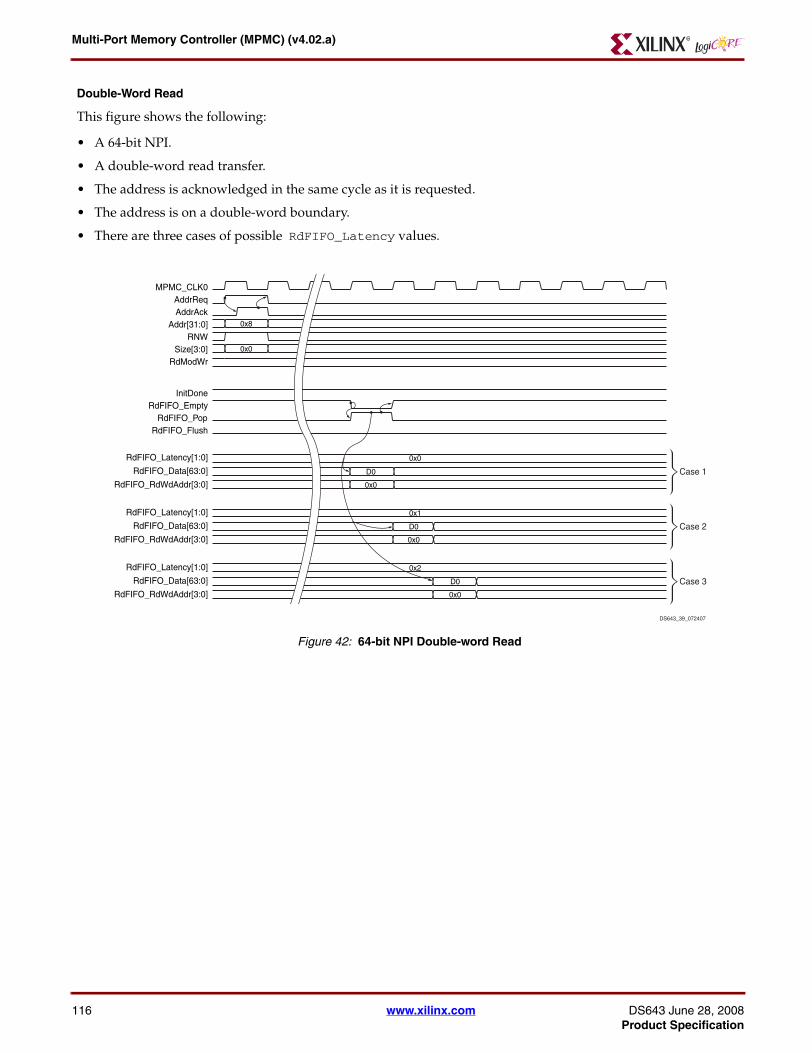
Multi-Port Memory Controller (MPMC) (v4.02.a)
Double-Word Read
This figure shows the following:
• A 64-bit NPI.
• A double-word read transfer.
• The address is acknowledged in the same cycle as it is requested.
• The address is on a double-word boundary.
• There are three cases of possible RdFIFO_Latency values.
Figure Top x-ref 38
Figure 42: 64-bit NPI Double-word Read
MPMC_CLK0AddrReq
Size[3:0]
RdFIFO_Empty
RdFIFO_RdWdAddr[3:0]
0x0
0x8
RNW
RdModWr
InitDone
RdFIFO_Latency[1:0]
RdFIFO_Pop
Addr[31:0]
D0
0x2
AddrAck
RdFIFO_Data[63:0]
0x0
RdFIFO_Flush
DS643_39_072407
Case 3
RdFIFO_RdWdAddr[3:0]
RdFIFO_Latency[1:0]
D0
0x1
RdFIFO_Data[63:0]
0x0
Case 2
RdFIFO_RdWdAddr[3:0]
RdFIFO_Latency[1:0]
D0
0x0
RdFIFO_Data[63:0]
0x0
Case 1
116 www.xilinx.com DS643 June 28, 2008Product Specification

Multi-Port Memory Controller (MPMC) (v4.02.a)
8-Word, Cacheline Write
This figure shows the following:
• A 64-bit NPI.
• An 8-word, cacheline write transfer.
• The address is acknowledged in the same cycle as it is requested.
• The address is on an 8-word boundary.
• The RdModWr does not need to be asserted because WrFIFO_BE is 0xFF during WrFIFO_Push, and because the 8-word transfer is larger than maximum value of 4*C_MEM_DATA_WIDTH. RdModWr is discussed in "Error Correction Code" page 128.
• Write Transfer Safe Mode (AddrReq asserted on same cycle as last WrFIFO_push.)
Figure Top x-ref 39
Figure 43: 64-bit NPI 8-word Cacheline Write
MPMC_CLK0AddrReq
Size[3:0]
WrFIFO_Empty
0x2
0x20
RNW
RdModWr
InitDone
WrFIFO_AlmostFull
Addr[31:0]AddrAck
WrFIFO_Push
DS643_40_072407
WrFIFO_BE[7:0]
WrFIFO_Flush
D0 D1 D2 D3WrFIFO_Data[63:0]
0xFF
117 www.xilinx.com DS643 June 28, 2008Product Specification
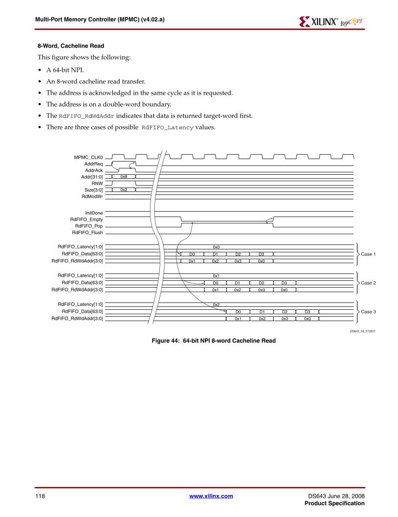
Multi-Port Memory Controller (MPMC) (v4.02.a)
607
3
2
1
8-Word, Cacheline Read
This figure shows the following:
• A 64-bit NPI.
• An 8-word cacheline read transfer.
• The address is acknowledged in the same cycle as it is requested.
• The address is on a double-word boundary.
• The RdFIFO_RdWdAddr indicates that data is returned target-word first.
• There are three cases of possible RdFIFO_Latency values.
Figure 44: 64-bit NPI 8-word Cacheline Read
MPMC_CLK0AddrReq
Size[3:0]
RdFIFO_Empty
RdFIFO_RdWdAddr[3:0]
0x2
0x8
RNW
RdModWr
InitDone
RdFIFO_Latency[1:0]
RdFIFO_Pop
Addr[31:0]
D0
0x2
AddrAck
RdFIFO_Data[63:0]
0x1
RdFIFO_Flush
DS643_58_072
Case
RdFIFO_RdWdAddr[3:0]
RdFIFO_Latency[1:0]
D0
0x1
RdFIFO_Data[63:0]
0x1
Case
RdFIFO_RdWdAddr[3:0]
RdFIFO_Latency[1:0]
D0
0x0
RdFIFO_Data[63:0]
0x1
D1
0x2
D1
0x2
D1
0x2
D2
0x3
D2
0x3
D2
0x3
D3
0x0
D3
0x0
D3
0x0
Case
118 www.xilinx.com DS643 June 28, 2008Product Specification

Multi-Port Memory Controller (MPMC) (v4.02.a)
32-Word, Burst Write
This figure shows the following:
• A 64-bit NPI.
• A 32-word, burst write transfer.
• The address is acknowledged in the same cycle as it is requested.
• The address is on a 32-word boundary.
• The RdModWr does not need to be asserted because WrFIFO_BE is 0xFF during WrFIFO_Push, and because a 32-word transfer is larger than maximum value of 4*C_MEM_DATA_WIDTH.
• The Write Transfer Safe Mode is used (AddrReq is asserted on same cycle as the last WrFIFO_push.)
Figure 45: 64-bit NPI 32-word Burst Write
MPMC_CLK0AddrReq
Size[3:0]
WrFIFO_Empty
0x4
0x80
RNW
RdModWr
InitDone
WrFIFO_AlmostFull
Addr[31:0]AddrAck
WrFIFO_Push
DS643_41_072407
WrFIFO_BE[7:0]
WrFIFO_Flush
D0 D1 D2 D3 D4 D5 D6 D7 D8 D9 D10 D11 D12 D13 D14 D15WrFIFO_Data[63:0]
0xFF
119 www.xilinx.com DS643 June 28, 2008Product Specification

Multi-Port Memory Controller (MPMC) (v4.02.a)
32-Word, Burst Read
This figure shows the following:
• A 64-bit NPI.
• A 32-word, burst read transfer.
• The address is acknowledged in the same cycle as it is requested.
• The address is on a double-word boundary.
• There are three cases of possible RdFIFO_Latency values.
Figure 46: 64-bit NPI 32-word Burst Read
DS643_42_072407
Case 3
Case 2
RdFIFO_RdWdAddr[3:0]
RdFIFO_Latency[1:0]
RdFIFO_Data[63:0] Case 1
MPMC_CLK0AddrReq
Size[3:0]
RdFIFO_Empty
0x4
0x80
RNW
RdModWr
InitDone
Addr[31:0]AddrAck
RdFIFO_Pop
RdFIFO_Flush
D0 D1 D2 D3 D4 D5 D6 D7 D8 D9 D10 D11 D12 D13 D14 D15
0x0
0x0
RdFIFO_RdWdAddr[3:0]
RdFIFO_Latency[1:0]
RdFIFO_Data[63:0] D0 D1 D2 D3 D4 D5 D6 D7 D8 D9 D10 D11 D12 D13 D14 D15
0x0
0x1
RdFIFO_RdWdAddr[3:0]
RdFIFO_Latency[1:0]
RdFIFO_Data[63:0] D0 D1 D2 D3 D4 D5 D6 D7 D8 D9 D10 D11 D12 D13 D14 D15
0x0
0x2
120 www.xilinx.com DS643 June 28, 2008Product Specification

Multi-Port Memory Controller (MPMC) (v4.02.a)
8-Word, Cacheline Write with Almost Full Flag Asserted
This figure shows the following:
• A 64-bit NPI.
• An 8-word, cacheline write transfer.
• The WrFIFO_AlmostFull is asserted on same cycle as the third WrFIFO_Push. The fourth WrFIFO_Push and AddrReq are delayed until after WrFIFO_AlmostFull is deasserted.
• The address is acknowledged in the same cycle as it is requested.
• The address is on an 8-word boundary.
• The RdModWr does not need to be asserted because WrFIFO_BE is 0xFF during WrFIFO_Push, and because an 8-word transfer is larger than maximum value of 4*C_MEM_DATA_WIDTH.
• The Write Transfer Safe Mode is used (AddrReq is asserted on same cycle as the last WrFIFO_push.)
Figure Top x-ref 40
Figure 47: 64-bit NPI 8-Word Cache-line Write with Almost Full Flag Asserted
DS643_43_072
MPMC_CLK0AddrReq
Size[3:0]
WrFIFO_Empty
0x2
0x20
RNW
RdModWr
InitDone
WrFIFO_AlmostFull
Addr[31:0]AddrAck
WrFIFO_Push
WrFIFO_BE[7:0]
WrFIFO_Flush
D0 D1 D2 D3WrFIFO_Data[63:0]
0xFF
121 www.xilinx.com DS643 June 28, 2008Product Specification

Multi-Port Memory Controller (MPMC) (v4.02.a)
8-Word, Cacheline Read with Back-to-Back Transfers
This figure shows the following:
• A 64-bit NPI.
• There are two back-to-back, 8-word burst, read transfers.
• First address acknowledged same cycle as requested.
• Second address is acknowledged cycle after request.
• There is no gap between address requests.
• The addresses are on double-word boundaries.
• The RdFIFO_RdWdAddr indicates that data is returned target-word first.
• There is a one cycle gap between read data for first request and second request. This could be more or less cycles depending on arbitration and pipeline settings.
• There are three cases of possible RdFIFO_Latency values.
Figure Top x-ref 41
Figure 48: 64-Bit, NPI 8-Word Cacheline Read with Back-to-Back Transfers
DS643_44_072407
MPMC_CLK0AddrReq
Size[3:0]
RdFIFO_Empty
0x2
0x10
R0 R1
R0 R1
RNW
RdModWr
InitDone
Addr[31:0]
0x2
0x28
AddrAck
RdFIFO_Pop
RdFIFO_Flush
Case 3
Case 2
RdFIFO_RdWdAddr[3:0]
RdFIFO_Latency[1:0]
RdFIFO_Data[63:0] Case 1D00 D10 D20 D30 D01 D11 D21 D31
0x2 0x3 0x0 0x1 0x3 0x0 0x1 0x2
0x2 0x3 0x0 0x1 0x3 0x0 0x1 0x2
0x2 0x3 0x0 0x1 0x3 0x0 0x1 0x2
D00 D10 D20 D30 D01 D11 D21 D31
D00 D10 D20 D30 D01 D11 D21 D31
0x0
RdFIFO_RdWdAddr[3:0]
RdFIFO_Latency[1:0]
RdFIFO_Data[63:0]0x1
RdFIFO_RdWdAddr[3:0]
RdFIFO_Latency[1:0]
RdFIFO_Data[63:0]0x2
122 www.xilinx.com DS643 June 28, 2008Product Specification

Multi-Port Memory Controller (MPMC) (v4.02.a)
32-Word, Burst Read with Read FIFO Flush Asserted
This figure shows the following:
• A 64-bit NPI.
• An 18-word, burst read transfer (a 32-word burst read transfer that is terminated by RdFIFO_Flush.)
• The address is acknowledged in the same cycle as it is requested.
• The address is on a 32-word boundary.
• There are three cases of possible RdFIFO_Latency values.
Figure Top x-ref 42
Figure 49: 64-Bit NPI 32-word Burst Read with Read FIFO Flush Asserted
DS643_45_072407
Case 3
Case 2
RdFIFO_RdWdAddr[3:0]
RdFIFO_Latency[1:0]
RdFIFO_Data[63:0] Case 1
MPMC_CLK0AddrReq
Size[3:0]
RdFIFO_Empty
0x4
0x80
RNW
RdModWr
InitDone
Addr[31:0]AddrAck
RdFIFO_Pop
RdFIFO_Flush
D0 D1 D2 D3 D4 D5 D6 D7 D8
0x0
RdFIFO_RdWdAddr[3:0]
RdFIFO_Latency[1:0]
RdFIFO_Data[63:0] D0 D1 D2 D3 D4 D5 D6 D7 D8
0x1
RdFIFO_RdWdAddr[3:0]
RdFIFO_Latency[1:0]
RdFIFO_Data[63:0] D0 D1 D2 D3 D4 D5 D6 D7 D8
0x2
123 www.xilinx.com DS643 June 28, 2008Product Specification

Multi-Port Memory Controller (MPMC) (v4.02.a)
32-Bit NPI Timing Diagrams
The following 32-bit NPI timing diagrams are illustrated:
• "Word Write"
• "Word Read"
• "8-Word, Cacheline Write"
• "8-Word, Cacheline Read"
Word Write
This figure shows the following:
• A 32-bit NPI.
• A word write transfer.
• The address is acknowledged in the same cycle as it is requested.
• The address is on a word boundary.
• The RdModWr must be asserted because the value of C_MEM_DATA_WIDTH is unknown.
• The Write Transfer Special Case is used (WrFIFO_Push is asserted after AddrAck.)
Figure Top x-ref 43
Figure 50: 32-Bit NPI Word Write
DS643_46_072407
MPMC_CLK0AddrReq
Size[3:0]
WrFIFO_Empty
WrFIFO_BE[3:0]
0x0
0x4
RNW
RdModWr
InitDone
WrFIFO_Flush
WrFIFO_AlmostFull
Addr[31:0]
D0
AddrAck
WrFIFO_Data[31:0]0xF
WrFIFO_Push
124 www.xilinx.com DS643 June 28, 2008Product Specification

Multi-Port Memory Controller (MPMC) (v4.02.a)
Word Read
This figure shows the following:
• A 32-bit NPI.
• A word read transfer.
• The address acknowledged same cycle as requested.
• The address is on a word boundary.
• There are three cases of possible RdFIFO_Latency values. Figure Top x-ref 44
Figure 51: 32-Bit NPI Word Read
DS643_47_072407
Case 3
Case 2
RdFIFO_RdWdAddr[3:0]
RdFIFO_Latency[1:0]
RdFIFO_Data[31:0] Case 1
MPMC_CLK0AddrReq
Size[3:0]
RdFIFO_Empty
0x0
0x4
RNW
RdModWr
InitDone
Addr[31:0]AddrAck
RdFIFO_Pop
RdFIFO_Flush
0x0
0x0
RdFIFO_RdWdAddr[3:0]
RdFIFO_Latency[1:0]
RdFIFO_Data[31:0]
0x0
0x1
RdFIFO_RdWdAddr[3:0]
RdFIFO_Latency[1:0]
RdFIFO_Data[31:0]
0x0
0x2
D0
D0
D0
125 www.xilinx.com DS643 June 28, 2008Product Specification

Multi-Port Memory Controller (MPMC) (v4.02.a)
8-Word, Cacheline Write
This figure shows the following:
• A 32-bit NPI.
• An 8-word, cacheline write transfer.
• The address is acknowledged in the same cycle as it is requested.
• The address is on an 8-word boundary.
• The RdModWr does not need to be asserted because WrFIFO_BE is 0xF during WrFIFO_Push, and because the 8-word transfer is larger than the maximum value of 4*C_MEM_DATA_WIDTH.
• The Write Transfer Safe Mode is use (AddrReq is asserted on the same cycle as the last WrFIFO_push.
Figure 52: 32-Bit NPI 8-word Cacheline Write
MPMC_CLK0AddrReq
Size[3:0]
WrFIFO_Empty
0x2
0x20
RNW
RdModWr
InitDone
WrFIFO_AlmostFull
Addr[31:0]AddrAck
WrFIFO_Push
DS643_48_072407
WrFIFO_BE[3:0]
WrFIFO_Flush
D0 D1 D2 D3 D4 D5 D6 D7WrFIFO_Data[31:0]
0xF
126 www.xilinx.com DS643 June 28, 2008Product Specification

Multi-Port Memory Controller (MPMC) (v4.02.a)
8-Word, Cacheline Read
This figure shows the following:
• A 32-bit NPI.
• An 8-word cacheline read transfer.
• The address is acknowledged in the same cycle as it is requested.
• The address is on a word boundary.
• The RdFIFO_RdWdAddr indicates that data is returned target-word first.
• There are three cases of possible RdFIFO_Latency values.
Figure 53: 32-Bit NPI 8-word Cacheline Read
AddrReq
Size[3:0] 0x2
0x4
RNW
RdModWr
Addr[31:0]AddrAck
DS643_49_072407
MPMC_CLK0
RdFIFO_EmptyInitDone
RdFIFO_Pop
RdFIFO_Flush
Case 3
Case 2
RdFIFO_RdWdAddr[3:0]
RdFIFO_Latency[1:0]
RdFIFO_Data[31:0] Case 1D0 D1 D2 D3 D4 D5 D6 D7
0x1 0x2 0x3 0x4 0x5 0x6 0x7 0x0
D0 D1 D2 D3 D4 D5 D6 D7
0x1 0x2 0x3 0x4 0x5 0x6 0x7 0x0
D0 D1 D2 D3 D4 D5 D6 D7
0x1 0x2 0x3 0x4 0x5 0x6 0x7 0x0
0x0
RdFIFO_RdWdAddr[3:0]
RdFIFO_Latency[1:0]
RdFIFO_Data[31:0]0x1
RdFIFO_RdWdAddr[3:0]
RdFIFO_Latency[1:0]
RdFIFO_Data[31:0]0x2
127 www.xilinx.com DS643 June 28, 2008Product Specification

Multi-Port Memory Controller (MPMC) (v4.02.a)
128
Error Correction CodeThe Error Correction Code (ECC) is optionally enabled via the C_INCLUDE_ECC_SUPPORT parameter control.
The ECC features are:
• Supports 8-, 16-, 32-, and 64-bit wide SDRAM, DDR and DDR2 memories.
• Provides Single Error Correction (SEC) and Double Error Detect (DED).
• Can generate interrupts when the number and type of errors reach a programmed threshold value.
Note: Spartan-3 MIG PHY does not support ECC.
Implementation
ECC functionality is implemented by inserting the ECC decode and encode logic between the Physical Interface (PHY) and Data Path of the MPMC. The following figure shows the current MPMC PHY Data Path connection for DDR/DDR2 memory.
The PHY interface converts the Double Data Rate (DDR) data from the memory into a Single Data Rate (SDR) bus that is twice as wide as the memory width. For SDRAM, data stays the same width through the PHY.
Because MPMC supports 8-, 16-, 32-, and 64-bit SDRAM and DDR/DDR2 memory, this results in an SDR bus that is 8-, 16-, 32-, 64-, or 128-bit wide going to the data path module. The data path module implements the per-port FIFOs used by MPMC.
Figure 55 on page 129 illustrates the changes that are made when ECC is enabled with DDR/DDR2 memory.
Figure 54: MPMC PHY-Data Path Connection
Data Path
Write
Read FIFO(s)
FIFO(s)NPI
NPI
DDR/DDR2Data
PHY Interface
SDR ReadData
8/16/32/64/128 Bits Wide
SDR WriteData
SDR MaskData
8/16/32/64/128 Bits Wide
8/16/32/64Bits Wide
X10918
www.xilinx.com DS643 June 28, 2008Product Specification

Multi-Port Memory Controller (MPMC) (v4.02.a)
X10919
When ECC functionality is enabled, several blocks are turned on to implement control and status registers, ECC decode and encode, and support for Read-Modify-Write (RMW) operations (needed for handling byte enables).
Note: All writes are RMW in the MPMC core once ECC is enabled.
The blocks are inserted between the PHY and data path so only one instance of the ECC logic is needed for multi-ple port configurations. The ECC decode and encode is performed in the SDR domain.
The ECC Control and Status registers module controls when interrupts are generated and provides control and sta-tus data access with respect to ECC. Refer to Table 23 on page 27 for more information on ECC Control and Status registers.
Read Data Handling
On Reads, data passes through the ECC Error Detection and Correction block. The data is checked for errors. If there are no errors, data passes through as normal and goes into the Read FIFO as a normal read. If a single error is detected, the error is corrected automatically (SEC) and sent to the Read FIFO to complete as a normal read. If 2 errors are detected (DED), the data is not corrected but passed through unchanged and the problem is reported to the Control and Status registers.
Figure 55: Data Path with ECC Enabled
Data Path
Write
Read FIFO(s)
BRAM ReadData FIFO(for Read-Modify-Write,same width as SDRdata from PHY)
Byte Wide Muxes(for Read-Modify-Write,Provides read data for
masked off bytesduring writes)FIFO(s)NPI
NPI
DDR/DDR2Data
PHY Interface
ECC Check Bit
SDR ReadData
16/32/64/128 Bits Wide
SDR WriteDataSDR ECCWrite Data
8/16/32/64/128Bits Wide
Byte Enable/Mask Data
8/16/32/64Bits Wide
SDR MaskData
ECCParity
8Bits Wide
Encode
DIn DOut
ECC
DOut
ECC ErrorDetection/Correction
ECC Control/StatusRegisters
DOut
Status
DIn
0
129 www.xilinx.com DS643 June 28, 2008Product Specification

Multi-Port Memory Controller (MPMC) (v4.02.a)
130
Need for Read Modify Write
During writes to memory, a new set of ECC check bits must be written to memory along with write data. The ECC encoding process is handled by the ECC Check Bit Encode block. Read-Modify-Writes (RMW) operations are needed for write transactions where the byte enables that span the width of the ECC word on the SDR bus are not all On or Off. Because many ECC DIMMs do not have Data Mask (DM) pins, the RMW is required.
When byte enables do not exist or are not all On or all Off, the correct value of the ECC check bits are not known because not all the data across the ECC word is present.
The RMW operation first fetches the data value of the masked off byte lanes so the correct ECC check bits for the whole ECC word can be computed and written. RMW is accomplished by taking read data (after ECC decode and correction) and storing the data in a FIFO that is the same width as the SDR data bus. Later, as write data comes out of the Write FIFO, the masked off byte enables activate an MUX that routes read data to fill in the corresponding “holes” in the write data. The result is a complete set of data with which to compute the new ECC check bits. All resultant data is written to memory. Consequently, writes with any byte enables turned Off result in writes with all byte enables turned On. This has the side effect that masked-off write data is read, scrubbed, and written back.
The Control state machine is modified during a RMW operation to perform a full Read and then a full Write. Because the data is on the same memory page, an optimization is to skip the precharge and acti-vate commands between a read and a write. To optimize the space in the control path block RAM state machines, RMW operations will reuse the corresponding Read and Write state machines for the given transfer size. Special block RAM state machine bits are used to implement the chained RMW operation and to skip precharge and activate commands.
The RMW process does add latency to the design because a full Read must precede a Write. This can double the transaction time for Writes. Writes with all byte enables On or all Off are faster than Writes with mixed byte enables due to need for RMW. A flag bit is introduced into the NPI interface to allow the transactions to be qualified as needing or not needing RMW.
The C_PIM<Port_Num>_RdModWr flag bit informs the MPMC if transactions require RMW (= 1) or do not require RMW (= 0). The C_PIM<Port_Num>_RdModWr signal must be asserted with PIM<Port_Num>_AddrReq. The C_PIM<Port_Num>_RdModWr signal should be asserted with respect to the memory burst length of 4 and the ECC word size of the memory interface being used. Any NPI transfer sizes which are less than a 4 beat memory burst must assert C_PIM<Port_Num>_RdModWr.
For NPI interfaces that do not support the RMW, or are not able to set it dynamically, the value should default to 1 to ensure correct Write operations under all conditions. Dynamic RMW allows for write performance to be optimized when RMW is known to not be needed.
If all the byte enables are Off but a RMW operation is performed, data is still read, scrubbed, and writ-ten back. This would permit a custom NPI device to perform burst writes with byte enables all Off (and RdModWr = 1) to scrub memory. MPMC does not require the memory to support DM pins with ECC. DM pins can be connected, if needed, or left unconnected.
ECC encode functionality adds latency to Writes. RMW support adds one cycle of latency to multiplex in Read data (in addition to latency of the full Read transaction). The Control state machines support the additional cycles of latency between Write FIFO pop and data appearing at the PHY interface.
For debugging and testing, the ECC encode process allows you to insert single or double bit errors into the data being written for test purposes. The error insertion logic can be parameterized out.
www.xilinx.com DS643 June 28, 2008Product Specification

Multi-Port Memory Controller (MPMC) (v4.02.a)
DS643 JuneProduct Sp
Memory Organization and ECC Word Size
The following table describes the ECC word size and number of extra memory data bits needed for dif-ferent organizations of memory. The RdModWr flag must be set according to the alignment across the ECC word size over a memory burst length of 4. The PHY requires a full ECC byte lane to be present on the board even though fewer bits might be used by ECC algorithm due to the requirements of the data calibration algorithms used in the PHY.
Note: For DDR/DDR2, the ECC words are based on the SDR bus size. The PHY data calibration algorithm requires that a full ECC byte lane be present on the board although fewer bits might be used by the ECC algorithm.
ECC Registers
Table 23, “MPMC_CTRL ECC Register Descriptions,” on page 27 shows the ECC related registers which are included with the ECC logic for the MPMC when ECC is enabled (C_INCLUDE_ECC_SUPPORT = 1). The following subsections describe each register and provide the bit definitions.
ECC Control Register
The ECC Control Register (ECCC) determines if ECC check bits are generated during memory write operation and checked during a memory read operation. The ECCC also defines testing modes if enabled by the parameter C_INCLUDE_ECC_TEST.
Table 58: ECC Word Size
Memory Type
Memory Data Width
Physical Memory ECC Data Width
(C_NUM_ECC_BITS)ECC Word Size
DDR/DDR2 8 8 2 Instances of 8 + 5 Check Bits
DDR/DDR2 16 8 2 Instances of 16 + 6 Check Bits
DDR/DDR2 32 8 2 Instances of 32 + 7 Check Bits
DDR/DDR2 64 8 2 Instances of 64 + 8 Check Bits
SDRAM 8 5 8 + 5 Check Bits
SDRAM 16 6 16 + 6 Check Bits
SDRAM 32 7 32 + 7 Check Bits
SDRAM 64 8 64 + 8 Check Bits
28, 2008 www.xilinx.com 131ecification

Multi-Port Memory Controller (MPMC) (v4.02.a)
132
The following table describes the bit values for the ECCC register.
ECC Status Register
The ECC Status register (ECCS) in combination with the ECC Error Address register (ECCADDR) records the first occurrence of an error and latches information about the error until the error is cleared by writing to the ECCS.
The following table describes the bit values for the ECC Status register.
Table 59: ECCC Register Bit Definitions
Bit(s) NameCore
AccessReset Value
Description
0:26 Reserved
27 FORCE_PE R/W 0
Force Parity Field Bit Error (1): Available for testing and determines if parity field bit errors are forced in the data stored in the memory. See ECC Testing for more information.0 = No parity field bit errors are created1 = Parity field bit errors are forced in stored data
28 FORCE_DE R/W 0
Force Double-bit Error (1): Available for testing and determines if double-bit errors are forced in the data stored in the memory. 0 = No double-bit errors are created1 = Double-bit errors are forced in the stored data
29 FORCE_SE R/W 0
Force Single-bit Error (1): Available for testing and determines if single-bit errors are forced in the data stored in the memory. 0 = No single-bit errors are created1 = Single-bit errors are forced in the stored data
30 RE R/W 1(2) ECC Read Enable:0 = ECC read logic is bypassed1 = ECC read logic is enabled
31 WE R/W 1(2)ECC Write Enable:0 = ECC write logic is bypassed1 = ECC write logic is enabled
1. This bit is available only if C_INCLUDE_ECC_TEST = 12. Reset value is determined by parameter C_ECC_DEFAULT_ON.
If C_ECC_DEFAULT_ON = 1 then this bit is equal to 1 If C_ECC_DEFAULT_ON = 0, then this bit is equal to 0
Table 60: ECCS Register Bit Definitions
Bit(s) NameCore
AccessReset Value
Description
0:15 Reserved
16:19 ECC_ERR_SIZE R/ROW(1) 0000ECC Error Transaction Size. Records the size of the NPI transaction where the error occurred
www.xilinx.com DS643 June 28, 2008Product Specification

Multi-Port Memory Controller (MPMC) (v4.02.a)
DS643 JuneProduct Sp
ECC Single-Bit Error Count Register
The ECC Single-Bit Error Count register (ECCSEC) records the number of ECC single-bit errors that occurred during the memory transaction on the data bits only. When using the force error feature, the number of errors detected may not be as expected because the force error feature counts the number of memory data beats that have errors, not the number of NPI data beats that have errors. Because the Read_Modify_Write might read more data than NPI requested, the count can be misleading. The ECC logic will correct the detected single-bit errors. When the value in this register reaches 4095 (the max count), the next single-bit error detected is not counted. This count consumes 12-bits.
Note: Single bit errors occurring on ECC check bits are covered by the ECCPEC register.
The following table describes the bit values for the ECC Single-Bit Error Count register.
20 ECC_ERR_RNW R/ROW(1) 0
ECC ERROR Transaction Read/Write: Indicates if error occurred on a read transactions or a write transaction that employed a read-modify-write operation.
21:28 ECC_ERR_SYND R/ROW(1) 00000000
ECC Error Syndrome: Indicates the ECC syndrome value of the most recent memory transaction in which a single-bit error was detected. The 8-bit syndrome value indicates the data bit position in which an error was detected and corrected.
29 PE R/ROW(1) 0
Parity Field Bit Error: During a memory transaction an error was detected in a parity field bit.0 = No parity field bit errors detected.1 = Parity field bit error detected and corrected.
30 DE R/ROW(1) 0
Double-Bit Error:During a memory transaction a double-bit error was detected and is not correctable.0 = No double-bit errors were detected.1 = Double-bit error was detected.
31 SE R/ROW(1) 0
Single-Bit Error: During memory transaction a single-bit error was detected and corrected.0 = No single-bit errors were detected.1 = Single-bit error detected and corrected.
1. ROW = Reset On Write. Any write operation to the ECCSR will reset the register.
Table 61: ECCSEC Bit Definitions
Bit(s) NameCore
AccessReset Value
Description
0:19 Reserved
20:31 SEC R/ROW(1) 0Single-Bit Error Count. Indicates the number of single-bit errors that occurred during the pervious memory transactions. The maximum error count is 4095.
1. ROW = Reset On Write. Any write operation to the ECCSEC register will reset the register.
Table 60: ECCS Register Bit Definitions (Continued)
Bit(s) NameCore
AccessReset Value
Description
28, 2008 www.xilinx.com 133ecification

Multi-Port Memory Controller (MPMC) (v4.02.a)
134
ECC Double-Bit Error Count Register
The ECC Double-Bit Error Count Register (ECCDEC) records the number of ECC double-bit errors that occurred during the memory transaction. ECC cannot correct double-bit errors detected. When the value in this register reaches 4095 (the max count), the next double-bit error detected is not counted. When using the force error feature, the number of errors detected may not be as expected because the force error feature counts the number of memory data beats that have errors, not the number of NPI data beats that have errors. Because the Read_Modify_Write might read more data than NPI requested, the count can be misleading. The ECC logic will correct the detected single-bit errors. When the value in this register reaches 4095 (the max count), the next single-bit error detected is not counted.
The following table describes the bit values for the ECCDEC.
ECC Parity Field Bit Error Count Register
The ECC Parity Field Bit Error Count Register (ECCPEC) records the number of bit errors that occurred in the ECC parity field during the memory transaction. ECC logic will correct detected parity field bit errors. When the value in this register reaches 4095 (the maximum count), the next parity field bit error detected is not counted. When using the force error feature, the number of errors detected may not be as expected because the force error feature counts the number of memory data beats that have errors, not the number of NPI data beats that have errors. Because the Read_Modify_Write might read more data than NPI requested, the count can be misleading. The ECC logic will correct the detected single-bit errors. When the value in this register reaches 4095 (the max count), the next single-bit error detected is not counted.
The following table describes the bit values for the ECCPEC.
Table 62: ECCDEC Bit Definitions
Bit(s) NameCore
AccessReset Value
Description
0:19 Reserved
20:31 DEC R/ROW(1) 0Double-Bit Error Count: Indicates the number of double-bit errors that occurred during the pervious memory transactions. The maximum error count is 4095.
1. ROW = Reset On Write. Any write operation to the ECCDEC register will reset the register.
Table 63: ECCPEC Bit Definitions
Bit(s) NameCore
AccessReset Value
Description
0:19 Reserved
20:31 PEC R/ROW(1) 0Parity Field Bit Error Count: Indicates the number of errors that occurred in the parity field bits during the last memory transactions. The maximum error count is 4095.
1. ROW = Reset On Write. Any write operation to the ECCPEC register will reset the register.
www.xilinx.com DS643 June 28, 2008Product Specification

Multi-Port Memory Controller (MPMC) (v4.02.a)
DS643 JuneProduct Sp
ECC Error Address Register
The following table describes the bit values for the ECC Error Address (ECCADDR) register.
ECC Interrupt Descriptions
Device Global Interrupt Enable Register
The Device Global Interrupt Enable Register (DGIE) is used to globally enable the final interrupt output from the ECC interrupt service. The following table describes the bit values for the DGIE.
IP Interrupt Status Register
The IP Interrupt Status register (IPIS) is the interrupt capture register for the ECC logic. The following table describes the bit values for the IPIS.
Table 64: ECCADDR Register Bit Definitions
Bit(s) NameCore
AccessReset Value
Description
0:31 ECCERRADDR RO N/A
ECC Error Address: Indicates the physical ECC address corresponding to an ECC error reported by the ECC Status register (ECCS). This register value is only valid when an error is actively reported in the ECCS.
Table 65: DGIE Register Bit Definitions
Bit(s) Name Core Access Reset Value Description
0 GIE R/W 0Global Interrupt Enable:0 = Interrupts disabled.1 = Interrupts enabled.
1-31 Reserved
Table 66: IPIS Register Bit Definitions
Bit(s) NameCore
AccessReset Value
Description
0:28 Reserved
29 PE_IS R/TOW(1) 0
Parity Field Bit Error Interrupt Status: Indicates a parity field bit error has occurred during the memory data transaction. In the ECC module, parity field bit errors will be corrected as data is read from memory. This interrupt is for system monitoring only and does not indicate corrupt data.0 = Parity field bit error count is less than C_ECC_PEC_THRESHOLD.1 = Parity field bit error count is more than C_ECC_PEC_THRESHOLD.
30 DE_IS R/TOW(1) 0
Double-Bit Error Interrupt Status: Indicates a double-bit data error has occurred during the memory transaction. In the ECC module, double-bit errors can be detected, but not corrected. When this interrupt is asserted, the data read from memory is not valid.0 = Double-bit error count is less than C_ECC_DEC_THRESHOLD.1 = Double-bit error count is more than C_ECC_DEC_THRESHOLD.
28, 2008 www.xilinx.com 135ecification

Multi-Port Memory Controller (MPMC) (v4.02.a)
136
IP Interrupt Enable Register
The IP Interrupt Enable register (IPIE) has an enable bit for each defined bit of the IP Interrupt Status register. The following table describes the bit values for the ECC IPIE.
31 SE_IS R/TOW(1) 0
Single-Bit Error Interrupt Status: Indicates a single-bit error has been detected during the memory transaction. In the ECC module, single-bit errors will be detected and corrected. This interrupt is for system monitoring only and does not indicate corrupt data.0 = Single-bit error count is less than C_ECC_SEC_THRESHOLD.1 = Single-bit error count is more than C_ECC_SEC_THRESHOLD.
1. TOW is Toggle On Write. Writing a 1 to a bit position within the register causes the corresponding bit position in the register to toggle.
Table 67: IPIE Register Bit Definitions
Bit(s) NameCore
AccessReset Value
Description
0:28 Reserved
29 PE_IE R/W 0
Parity Field Bit Error Interrupt Enable: Enables assertion of the interrupt for indicating parity field bit errors have occurred. 0 = Disabled 1 = Enabled
30 DE_IE R/W 0
Double-bit Error Interrupt Enable: Enables assertion of the interrupt for indicating double-bit data errors have occurred.0 = Disabled1 = Enabled
31 SE_IE R/W 0
Single-bit Error Interrupt Enable: Enables assertion of the interrupt for indicating single-bit data errors have occurred. 0 = Disabled1 = Enabled
Table 66: IPIS Register Bit Definitions (Continued)
Bit(s) NameCore
AccessReset Value
Description
www.xilinx.com DS643 June 28, 2008Product Specification

Multi-Port Memory Controller (MPMC) (v4.02.a)
DS643 JuneProduct Sp
ECC TestingTo enable testing on the ECC core logic, set C_INCLUDE_ECC_TEST = 1. The ECC Control register (ECCCR), described in "ECC Control Register" page 131, includes control bits for enabling or disabling the test logic.
The following list describes possible forcing errors combinations. If any other combination is attempted, no errors will be forced on the data written to memory.
• No bit error forcing.
• Force single-bit data errors (ECC Control register (ECCC): FORCE_SE = 1).
• Force double-bit data errors (ECC Control register (ECCC): FORCE_DE = 1).
• Force parity bit errors (ECC Control register (ECCC): FORCE_PE = 1).
• Force single-bit data and single parity field bit errors (ECC Control register (ECCC): FORCE_SE = 1 and FORCE_PE = 1).
For single-bit error testing, a mask shift register forces single-bit errors on the data written to memory. The data mask shift register has the least significant single-bit equal to one. When testing is enabled during a memory write, the shift register clocks the one toward the Most Significant Bit (MSB). You must be careful when trying to predict the pattern. More memory data beats may be written than expected because the Read_Modify_Write will read a full “memory cacheline”, merge this with the data sent from the PIM, then write back the entire “memory cacheline”. This will result in a different rotation than you might expect.
For double-bit error testing, a data mask shift register forces double-bit errors on the data written to memory. The data mask shift register has two adjacent bits equal to one (starting in the two least signif-icant bit positions) and rotates the “11” pattern in the shift register (towards the two most significant bits) on each memory write.
When parity field bit error testing is enabled, a mask shift register forces single-bit errors on the check bits stored in memory. The parity mask shift register has the least significant single-bit equal to one and rotates the one (toward the MSB) on each memory write.
28, 2008 www.xilinx.com 137ecification

Multi-Port Memory Controller (MPMC) (v4.02.a)
138
Performance MonitoringThe MPMC Performance Monitor (PM) is an optional per-port feature that can be used to count trans-action lengths across each NPI interface. The PM provides the ability to instrument and measure the performance of the MPMC by collecting transactional statistics at the NPI level relative to the memory clock rate. Each PM is capable of capturing the duration, size, read or write, and dead cycle counts of each transaction. These are stored into a block RAM and are retrievable over the MPMC_CTRL Slave PLB v.46 interface. To use PMs on a specific port, that port must have the Address Acknowledge Pipe-line enabled to ensure correct operation. PM cycle counts only represent transactions across the NPI interface and do not include latency of attached PIMs or user NPI logic.
The PM provides:
• An optional configurable length global cycle counter.
• An optional configurable length arbitration dead cycle counter for each port.
• The MPMC_CTRL Slave PLB v.46 interface to control and collect data from the Performance Monitors.
• A performance monitor state machine and data collector consuming one block RAM per port enabled.
• PM registers.
Performance Monitor Operation
The following subsections provide an outline of the PM measurement methodology and give an exam-ple of the steps in a PM monitoring session.
Performance Monitor Measurement Methodology
The cycle counts recorded in each data bin is recorded as following:
• Data Bin Read Transactions: Number of memory clock cycles from NPI_<PortNum>AddrReq until last data is popped from data FIFO.
• Data Bin Write Transactions: Number of memory clock cycles from NPI_<PortNum>AddrReq until the later of NPI_<PortNum>AddrAck or the last push into the data FIFO.
• Global Cycle Counter: Counts each memory clock cycle after at least one PM is enabled.
• Dead Cycle Counter: Counts the number of memory cycles from NPI_<PortNum>AddrReq until granted by NPI_<PortNum>AddrAck.
Example Usage
An example PM session includes the following steps:
1. Disable any currently enabled PMs by writing zeros to the Performance Monitor Control Register.2. Clear the PM counters by writing ones to the Performance Monitor Clear Register.3. Wait for the clear operation to complete by polling the Performance Monitor Status Register for all
PMs bits set as one.4. Clear PM status by writing ones to the Performance Monitor Status Register.5. Enable PM counting by writing ones to the Performance Monitor Control Register.6. Execute user task to be monitored.7. Stop the PM counting by writing ones to the Performance Monitor Control Register.
www.xilinx.com DS643 June 28, 2008Product Specification

Multi-Port Memory Controller (MPMC) (v4.02.a)
DS643 JuneProduct Sp
8. Read each data bin value, typically looping through each set of 32 data bins, read/write set, qualifier set, and finally each PM.
9. Read the Performance Monitor Global Cycle Count Register for total test time.10. Read the Performance Monitor Dead Cycle Count Register of each PM for cycles lost to arbitration
grant delays.11. Prepare for next task monitoring by either re enabling the PMs or executing the clear process.
Performance Monitor Registers
PM registers detailed in the following subsections are available that perform these actions:
• Capture performance statistics (PMCTRL)
• Monitor the status of the clear issued to the PM data bins (PMSTATUS)
• Contain the current value of the global cycle counter (PMGCC)
• Contain the current value of the dead cycle counter for each port (PMx_DCC)
• Contain the transaction information for the performance monitors (PMx_DATA_BINx)
Performance Monitor Control Register
The Performance Monitor Control Register (PMCTRL) sets the enable bits for performance monitors to capture statistics and place them in the data bins. Initially, the performance monitors are not enabled and the data bins are initialized to 0.
The performance monitor enable bit should be set to 0 when reading back data to maintain consistent data across all the data bins. Setting the performance monitor enable bit to 1 will immediately start cap-turing data and also enable the dead cycle counters, if the parameter is enabled. If the global cycle counter is enabled, it will count when any of the enable bits are high. The following table describes the PMCTRL register bits.
Table 68: PMCTRL Register Bit Definitions
Bit(s) NameCore
AccessReset Value
Description
0 PM0_ENABLE R/W 01 = Enable PM00 = Disable PM0
1 PM1_ENABLE R/W 01 = Enable PM10 = Disable PM1
2 PM2_ENABLE R/W 01 = Enable PM20 = Disable PM2
3 PM3_ENABLE R/W 01 = Enable PM30 = Disable PM3
4 PM4_ENABLE R/W 01 = Enable PM40 = Disable PM4
5 PM5_ENABLE R/W 01 = Enable PM50 = Disable PM5
6 PM6_ENABLE R/W 01 = Enable PM60 = Disable PM6
7 PM7_ENABLE R/W 01 = Enable PM70 = Disable PM7
8:31 Reserved Reserved
28, 2008 www.xilinx.com 139ecification

Multi-Port Memory Controller (MPMC) (v4.02.a)
140
Performance Monitor Clear Register
The Performance Monitor Clear Register (PMCLR) facilitates clearing the block RAMs used for the PM data bins back to 0. It also used to clear the dead cycle counters and global cycle counter to 0. This reg-ister is a write only register. Writing a 1 to the clear bits will immediately clear the counters, and start the clearing of the data bins. Because the data bins are stored in a block RAM, it will take approximately 512 clock cycles to clear the data bins to 0. To monitor the status of the clear, please see the PMSTATUS register.
The following table describes the PMCLR register bits.
Table 69: PMCLR Register Bit Definitions
Bit(s) NameCore
AccessReset Value
Description
0 PM0_DATABIN_CLR W X 1 = Clear all data bin storage PM0
1 PM1_DATABIN_CLR W X 1 = Clear all data bin storage PM1
2 PM2_DATABIN_CLR W X 1 = Clear all data bin storage PM2
3 PM3_DATABIN_CLR W X 1 = Clear all data bin storage PM3
4 PM4_DATABIN_CLR W X 1 = Clear all data bin storage PM4
5 PM5_DATABIN_CLR W X 1 = Clear all data bin storage PM5
6 PM6_DATABIN_CLR W X 1 = Clear all data bin storage PM6
7 PM7_DATABIN_CLR W X 1 = Clear all data bin storage PM7
8:22 Reserved Reserved
23:31 Reserved Reserved
www.xilinx.com DS643 June 28, 2008Product Specification
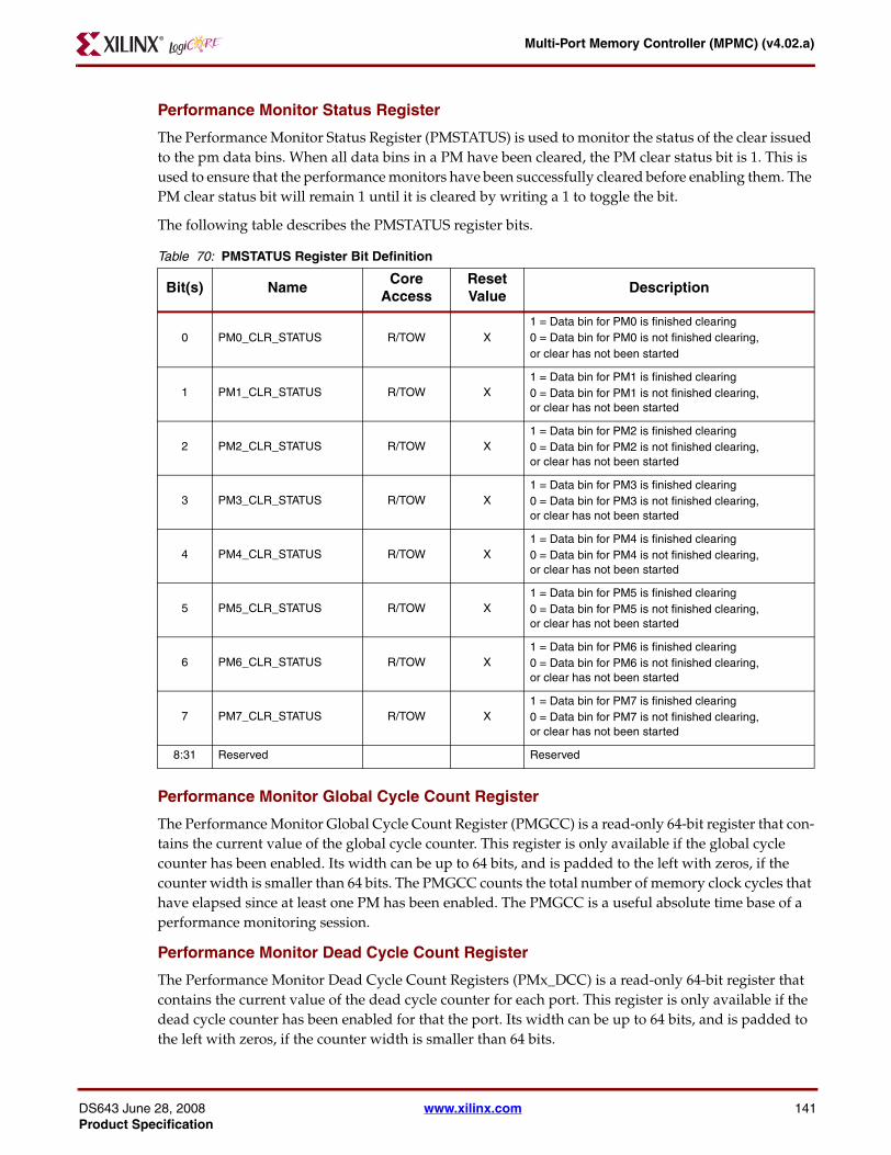
Multi-Port Memory Controller (MPMC) (v4.02.a)
DS643 JuneProduct Sp
Performance Monitor Status Register
The Performance Monitor Status Register (PMSTATUS) is used to monitor the status of the clear issued to the pm data bins. When all data bins in a PM have been cleared, the PM clear status bit is 1. This is used to ensure that the performance monitors have been successfully cleared before enabling them. The PM clear status bit will remain 1 until it is cleared by writing a 1 to toggle the bit.
The following table describes the PMSTATUS register bits.
Performance Monitor Global Cycle Count Register
The Performance Monitor Global Cycle Count Register (PMGCC) is a read-only 64-bit register that con-tains the current value of the global cycle counter. This register is only available if the global cycle counter has been enabled. Its width can be up to 64 bits, and is padded to the left with zeros, if the counter width is smaller than 64 bits. The PMGCC counts the total number of memory clock cycles that have elapsed since at least one PM has been enabled. The PMGCC is a useful absolute time base of a performance monitoring session.
Performance Monitor Dead Cycle Count Register
The Performance Monitor Dead Cycle Count Registers (PMx_DCC) is a read-only 64-bit register that contains the current value of the dead cycle counter for each port. This register is only available if the dead cycle counter has been enabled for that the port. Its width can be up to 64 bits, and is padded to the left with zeros, if the counter width is smaller than 64 bits.
Table 70: PMSTATUS Register Bit Definition
Bit(s) NameCore
AccessReset Value
Description
0 PM0_CLR_STATUS R/TOW X1 = Data bin for PM0 is finished clearing0 = Data bin for PM0 is not finished clearing, or clear has not been started
1 PM1_CLR_STATUS R/TOW X1 = Data bin for PM1 is finished clearing0 = Data bin for PM1 is not finished clearing, or clear has not been started
2 PM2_CLR_STATUS R/TOW X1 = Data bin for PM2 is finished clearing0 = Data bin for PM2 is not finished clearing, or clear has not been started
3 PM3_CLR_STATUS R/TOW X1 = Data bin for PM3 is finished clearing0 = Data bin for PM3 is not finished clearing, or clear has not been started
4 PM4_CLR_STATUS R/TOW X1 = Data bin for PM4 is finished clearing0 = Data bin for PM4 is not finished clearing, or clear has not been started
5 PM5_CLR_STATUS R/TOW X1 = Data bin for PM5 is finished clearing0 = Data bin for PM5 is not finished clearing, or clear has not been started
6 PM6_CLR_STATUS R/TOW X1 = Data bin for PM6 is finished clearing0 = Data bin for PM6 is not finished clearing, or clear has not been started
7 PM7_CLR_STATUS R/TOW X1 = Data bin for PM7 is finished clearing0 = Data bin for PM7 is not finished clearing, or clear has not been started
8:31 Reserved Reserved
28, 2008 www.xilinx.com 141ecification

Multi-Port Memory Controller (MPMC) (v4.02.a)
142
Each dead cycle count represents a NPI clock cycle where a request was not immediately acknowl-edged by the arbiter. This is useful to measure how many cycles a particular port has waited since per-formance monitoring was first enabled.
Dead cycles typically occur due to the MPMC controller processing older or higher priority port accesses or the memory being unavailable during external memory maintenance.
Performance Monitor Data Bin Registers
The Performance Monitor Data Bin Registers (PMx_DATA_BINx) contain the transaction information for the performance monitors. Each performance monitor contains 512 36-bit data bins. These values are read-only 36-bit registers that are padded with zeros on the left to expand them to 64 bits. Therefore, each performance monitor data bin will be 8 kb of data.
Each bin contains a count of transactions for a specific PM port, the NPI transaction type, the transac-tion direction, and the exact number or range of clock cycles elapsed. For example, one data bin on PIM port 2 might contain the total quantity of 32-word burst-type write transactions which lasted between 8 and 15 clock cycles since the PM was first enabled.
Data Bin Organization
Each PM is divided into eight qualifiers, indicating the transaction size. These qualifiers are then sub-divided into Writes and Reads. This allows 32 bins per qualifier each write and read. The bins them-selves represent the transaction length of that particular qualifier. The 36-bit number the bin contains represents how many times that transaction length has been counted.
Qualifier Definitions
The following table describes the qualifier definitions.
Qualifier Description
0 Byte – Double Words
1 Cache Line 4
2 Cache Line 8
3 Burst 16
4 Burst 32
5 Burst 64
6 Reserved
7 Reserved
www.xilinx.com DS643 June 28, 2008Product Specification

Multi-Port Memory Controller (MPMC) (v4.02.a)
DS643 JuneProduct Sp
Data Bin Organization
The following table describes the Data Bin organization.
Qualifier Type Access Type Bin No.Offset from
PMx_DATABINx
0
Write
0 0x000
1 0x008
… …
31 0x0F8
Read
0 0x100
1 0x108
… …
31 0x1F8
1
…
Write
0 0x200
1 0x208
… …
31 0x2F8
Read
…
0 0x300
1 0x308
… …
31 0x3F8
… …
7
Write
0 0xE00
1 0xE08
… …
31 0xEF8
Read
0 0xF00
1 0xF08
… …
31 0xFF8
28, 2008 www.xilinx.com 143ecification

Multi-Port Memory Controller (MPMC) (v4.02.a)
144
The bin number represents the length of the transaction in cycles shifted by the C_PM_SHIFT_BY parameter. This allows a trade between the maximum length of a transaction that can be recorded and the granularity of the transaction lengths. The number the bin contains is the number of times that par-ticular transaction length was recorded.
The following table shows the C_PM_SHIFT_BY relationship of Bin Number to Transaction Length.
C_PM_SHIFT_BY Bin NumberTransaction Length
(cycles)
0
0 0
1 1
… …
31 31+
1
0 0-1
1 2-3
… …
31 62-63+
2
0 0-3
1 4-7
… …
31 124-127+
3
0 0-7
1 8-15
… …
31 248-258+
www.xilinx.com DS643 June 28, 2008Product Specification

Multi-Port Memory Controller (MPMC) (v4.02.a)
DS643 JuneProduct Sp
IP Configuration Graphical User InterfaceThe IP Configuration interface offers a convenient and user-friendly way to configure a system. You can invoke the IP Configurator GUI within XPS by double-clicking the MPMC IP in the System Assembly View, or by right-clicking MPMC and selecting Configure IP. The tabs in the interface are:
• Base Configuration
• Memory Interface
• Port Configuration
• Advanced
To create a functional MPMC you need to use the following three tabs only:
• Base Configuration: select the port type for each active port and remove unused ports between active ports
• Memory Interface: select the memory part and configure the memory settings
• Port Configuration: set the parameters for each port
The Advanced tab contains advanced features such as per-port addresses, per-port data path configu-ration, arbitration algorithms, performance, and debugging. This tab is intended for advanced users only.
Base Configuration
MPMC provides up to eight ports for accessing the memory; each port can be configured to a different bus or port type. The Base Configuration tab lets you set:
• Port types of the eight available ports: the dropdown box contains INACTIVE, XCL, PLBv46, SDMA, NPI, PPC440MC, and VFBC.
• Common base addresses
The Port Configuration box contains an interface diagram of MPMC; under each port interface is a dropdown selection that lets you choose the port type. "Memory and Memory Part Parameters" page 10 contains a description of the parameter that specifies port types.
The LeftJustify button is for eliminating the inactive ports between active ports, which is desirable because inactive ports also consume logic. During this justifying process, all parameters related to the ports and external bus connections are shifted left accordingly. Below is an example representing the action that occurs with a left-justification of ports.
The Common Addresses box lets you enter common Base Addresses and SDMA Register Base Addresses. Common base addresses are used by every port for address decoding. For common SDMA addresses, each port has its own set of registers which are offset at a fixed size from the common SDMA base address.
To configure each individual port address, go to the Address option under the Advanced tab.
Port0 Port1 Port2 Port3 Port4 Port5 Port6 Port7
Before Left Justifying
XCL PLBv46 Inactive Inactive XCL Inactive SDMA Inactive
After Left Justifying
XCL PLBv46 XCL SDMA Inactive Inactive Inactive Inactive
28, 2008 www.xilinx.com 145ecification

Multi-Port Memory Controller (MPMC) (v4.02.a)
146
Memory Interface
MPMC can work with a wide variety of memory parts from different manufacturers. This tab lets you select the memory part used in conjunction with the MPMC.
MPMC has a list of supported memory devices. To select the device to meet your needs, use the Mem-ory Part Selector area, where available memory parts can be filtered based on the following criteria:
• Type – options are: DDR, DDR2, or SDRAM
• Memory manufacturer – options are: Hynix, Samsung, Micron, Infineon, SimpleTec, and WinTec
• Memory style – options are: DIMM, Discrete, or SODIMM
• Memory density – capacity of memory
• Memory width – data width of memory
The filtered results appear in the Part No. drop-down list. The Memory Part Selector/Part No. drop-down contains a CUSTOM option also, if the correct part is not available in the built-in memory data-base. After you select the CUSTOM option, all the memory parameters are editable and you can enter the parameters you require. After you have selected a memory part, its parameters are automatically loaded into the Selected Memory Info area and the Memory/DIMM Settings tab.
Note: If you select a similar memory part first and then select the CUSTOM option, the memory parameters from the first memory part are retained, but are the fields are editable. This can simplify the process of entering a CUSTOM memory part if it is in a format that is similar to one in the database.
Memory/DIMM Settings Tab
The Memory/DIMM Settings tab provides the following areas: Settings, Configuration, and Info.
Under the Settings area, selection and drop-down boxes are available where you can adjust:
• Number of DIMMs
• Memory Data Width
• Memory Clock Period (ps)
• ODT Setting
• Part Information
A check box is available for Reduced Drive Output also.
Based on the selected device, the appropriate parameters are editable.
The Configuration area provides selection options for CE Width, ODT Width, Clock Width, CSn Width, and No. of Ranks. A check box is available for Registered Memory also.
The Info area provides the following Memory Width options: DM, ADDr, Bank Addr, and DQS.
Memory Part Settings Tab
The Memory Part Settings tab has two areas: Part Settings and Memory Timing Settings.
• Part Settings contains options for selecting Data Depth, Data Width, Bank, Row, and Column Bits.
• Memory Timing Settings contains memory part options.
www.xilinx.com DS643 June 28, 2008Product Specification

Multi-Port Memory Controller (MPMC) (v4.02.a)
DS643 JuneProduct Sp
Port Configuration
In the Port Configuration tab you can configure the parameters of each individual port. Tabs are avail-able for Port 0-3 and Port 4-7. The Port tabs are divided into quadrants with a port number represented in each quadrant. Only the parameters related to the current port type (selected in the Base Configu-ration tab) are active and editable. For a detailed description of parameters, refer to "MPMC Per-port Parameters" page 6.
Advanced
The Advanced tab contains the tabs:
• Address Configuration
• Data Path
• Arbitration
• ECC/Debug
• Misc
These tabs offer more advanced customization of MPMC.
Address ConfigurationIn the Address Configuration tab, you can choose to ignore the common base addresses and configure the addresses of each individual port.
The Use Common Port Address check box is checked on by default. If you do not want to use com-mon port address, you can deselect the check box to disable the use of common port addresses and enable the Port Addresses box. You can then change the port addresses of each port.
The rows in the Port Addresses box are:
• Base Address: Base address of the port as specified by C_PIM<Port_Num>_BASEADDR which is described in Table 2 on page 6.
• High Address: High address of the port as specified by C_PIM<Port_Num>_HIGHADDR which is described in Table 2 on page 6.
• Offset: Address offset as specified by C_PIM<Port_Num>_OFFSET which is described in Table 2 on page 6. This allows a multi-processor system to have identical logic memory space inside each processor while mapping each logical memory space to different physical locations inside the memory.
• SDMA Control Port Base Address: logical base address of SDMA channel (if configured as SDMA).
• SDMA Control Port High Address: logical high address of SDMA channel (if configured as SDMA).
The Restore Default Addr button restores the address to common address mode.
28, 2008 www.xilinx.com 147ecification

Multi-Port Memory Controller (MPMC) (v4.02.a)
148
Data PathIn the Data Path tab, you can configure the common data path (pipeline) settings and the individual settings for each port.
General Pipeline Settings let you set the general pipeline parameters, and Port-specific Settings let you change the pipeline settings for the individual ports as follows:
• NPI Width: Width of Native Port Interface.
• Read FIFO Config: Implement FIFO using block RAM, SRL, or Wr-Only (Write Only, Read FIFO Disabled).
• Write FIFO Config: Implement FIFO using block RAM, SRL, or Rd-Only (Read Only, Write FIFO Disabled).
• Read Memory Pipeline: Enable pipeline for read access to memory.
• Read Port Pipeline: Enable pipeline for read access to the underlying port.
• Write Memory Pipeline: Enable pipeline for write access to memory.
• Write Port Pipeline: Enable pipeline for write access to port.
• Address Ack Pipeline: Enable pipeline for acknowledgement of address request.
ArbitrationMPMC has a maximum of eight ports that can all access the memory at the same time. Consequently, it is very important to have an arbitration algorithm to determine which port has priority at any given moment. In the Arbitration tab, you can choose what arbitration algorithm to use.
From the Select Arbitration Algorithm box, select one of the three following arbitration algorithms:
• Round Robin: Perform Round Robin arbitration.
• Fixed: Perform Fixed priority arbitration.
• Custom: In this mode, you can customize the number of time slots, as well as the arbitration priorities in each time slot. The arbitration priority in each time slot is encoded as a string to indicate decreasing priorities among ports. For example, the string “01234567” gives the highest priority to port 0, then decreasing priorities from port 1 through port 7.
ECC/Debug
In the ECC/Debug tab, you can set debug, Error Correction Code (ECC), and Performance Monitor (PM) related options. All debug registers, ECC registers and PMs are accessed using a Control bus interface.
In the General ECC/Debug Settings box, you can enable debug, ECC, and PM. If any one of them is enabled, the Control Bus is activated and you must enter the base address in the Control Base Address box.
After you enable ECC, you can configure the behavior further in the ECC Settings box.
After you enable PM, you can change the general parameters of the Performance Monitor in the Com-mon Performance Monitor Settings box, and the port-specific parameters in Port-specific Perfor-mance Monitor Settings box.
Misc
The Misc tab contains parameters that require your attention but do not fall into any of the previous categories.
www.xilinx.com DS643 June 28, 2008Product Specification

Multi-Port Memory Controller (MPMC) (v4.02.a)
DS643 JuneProduct Sp
System TimingNote: The following table lists the target operating frequency range for MPMC for a variety of FPGA device families and speed grades. These values provide guideline memory clock frequencies for MPMC.
The values shown in Table 71 are based on the following condition assumptions:
• Default parameters settings for MPMC
• 2:1 PIM clock ratios
• No use of floorplanning
• Default implementation tool options
Note: The target fMAX is influenced by the exact system and is provided for guidance. It is not a guaranteed value across all systems. The fMAX timing for the MPMC Performance Monitors has not been characterized and could be significantly lower. The fMAX timing for SDRAM has not been characterized and is likely to be limited by the physical system.
Table 71: Target Operating Frequency Ranges by FPGA Family
FPGA Family Target fMAX Range (MHz)
Spartan-3 Generation, -4 Speed Grade 125-133
Spartan-3 Generation, -5 Speed Grade 133-166
Virtex-4, -10 Speed Grade 165-185
Virtex-4, -11 Speed Grade 185-205
Virtex-4, -12 Speed Grade 200-225
Virtex-5, -1 Speed Grade 175-200
Virtex-5, -2 Speed Grade 185-220
Virtex-5, -3 Speed Grade 210-250
28, 2008 www.xilinx.com 149ecification
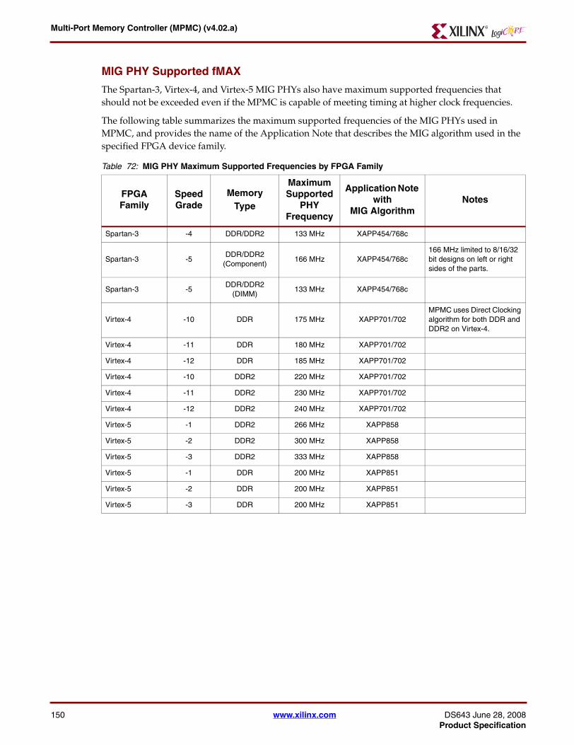
Multi-Port Memory Controller (MPMC) (v4.02.a)
150
MIG PHY Supported fMAX
The Spartan-3, Virtex-4, and Virtex-5 MIG PHYs also have maximum supported frequencies that should not be exceeded even if the MPMC is capable of meeting timing at higher clock frequencies.
The following table summarizes the maximum supported frequencies of the MIG PHYs used in MPMC, and provides the name of the Application Note that describes the MIG algorithm used in the specified FPGA device family.
Table 72: MIG PHY Maximum Supported Frequencies by FPGA Family
FPGA Family
Speed Grade
MemoryType
Maximum Supported
PHY Frequency
Application Note with
MIG AlgorithmNotes
Spartan-3 -4 DDR/DDR2 133 MHz XAPP454/768c
Spartan-3 -5DDR/DDR2
(Component)166 MHz XAPP454/768c
166 MHz limited to 8/16/32 bit designs on left or right sides of the parts.
Spartan-3 -5DDR/DDR2
(DIMM)133 MHz XAPP454/768c
Virtex-4 -10 DDR 175 MHz XAPP701/702MPMC uses Direct Clocking algorithm for both DDR and DDR2 on Virtex-4.
Virtex-4 -11 DDR 180 MHz XAPP701/702
Virtex-4 -12 DDR 185 MHz XAPP701/702
Virtex-4 -10 DDR2 220 MHz XAPP701/702
Virtex-4 -11 DDR2 230 MHz XAPP701/702
Virtex-4 -12 DDR2 240 MHz XAPP701/702
Virtex-5 -1 DDR2 266 MHz XAPP858
Virtex-5 -2 DDR2 300 MHz XAPP858
Virtex-5 -3 DDR2 333 MHz XAPP858
Virtex-5 -1 DDR 200 MHz XAPP851
Virtex-5 -2 DDR 200 MHz XAPP851
Virtex-5 -3 DDR 200 MHz XAPP851
www.xilinx.com DS643 June 28, 2008Product Specification

Multi-Port Memory Controller (MPMC) (v4.02.a)
DS643 JuneProduct Sp
Timing Improvement Tips
The following list identifies possible ways to improve timing of MPMC systems:
1. Experiment with different values for C_RD_DATAPATH_TML_MAX_FANOUT. All other pipeline stages are turned on by default.
2. Minimize the use of DCMs to synthesize the MPMC memory clock. If possible the board should provide a clock source that directly inputs the desired MPMC memory clock frequency.
3. MPMC timing can be greatly affected by block RAM placement. The use of block RAM floorplanning can greatly improve MPMC timing results. If the number of available block RAMs in a design is low, freeing up block RAM can improve timing. This is especially important on Virtex-5 designs.
4. If possible, use fixed arbitration.5. Move C_WR_TRAINING_PORT to a different port that is less timing critical (for example, using a
DXCL port instead of an SDMA port for the write training pattern).6. Minimize the number of ports.7. Run EDK in xplorer mode (this significantly increases the tool runtimes).
Resource UtilizationThe following subsections detail the MPMC resource utilization:
• "Resource (block RAM) Utilization"
• "Resource (LUT and Flip Flop) Utilization"
Resource (block RAM) Utilization
By default, MPMC uses block RAM based FIFOs in each of its ports to buffer read and write data from the external memory to improve memory efficiency, reduce LUT utilization, and to improve timing. MPMC also provides a per-port parameter called C_PI<Port_Num>_RD_FIFO_TYPE and C_PI<Port_Num>_WR_FIFO_TYPE which can be used to disable FIFOs for (read-only or write-only ports) or to choose the use of SRL FIFOs instead of block RAM FIFOs.
MPMC block RAM utilization is outlined as follows:
• 1 block RAM for control state machine.
• 1 block RAM for arbitration if CUSTOM arbitration algorithm is used (C_ARB0_ALGO = CUSTOM). For FIXED or ROUND_ROBIN arbitration no block RAM is used. If only 1 port is used no block RAM is used.
• If ECC is enabled, 1 block RAM is used for 8-, 16-, and 32-bit DDR/DDR2 memories, and two block RAMs for 64-bit DDR/DDR2 memories.
• 1 block RAM for every port where a Performance Monitor is enabled.
28, 2008 www.xilinx.com 151ecification

Multi-Port Memory Controller (MPMC) (v4.02.a)
152
The following table shows the block RAM usage for each Read and Write port:
To conserve block RAMs, the MPMC can be configured to use SRL FIFOs instead of block RAM FIFOs. With a 64-bit NPI:
• Each read SRL FIFO uses approximately 288 LUTs per port.
• Each write SRL FIFO uses approximately 256 LUTs per port.
The use of SRL FIFOs might negatively impact timing due to the slower speed of SRL FIFOs compared to block RAMs (BRAMs).
Resource (LUT and Flip Flop) Utilization
This section provides an estimate for Lookup Table (LUT) and Flip-Flop (FF) utilization of MPMC. The values provided are for resource estimation and are not guaranteed. These estimates assume default MPMC settings and default implementation tool options. Actual FPGA resource utilization depends on exact MPMC configuration parameters and implementation tool optimizations including cross bound-ary logic optimization, logic sharing, register re-timing, global system optimization, logic trimming, timing targets, and implementation tool settings.
Table 73: Read and Write Port block RAM Usage
Read Ports
0 block RAMs if write-only port (C_PI<Port_Num>_RD_FIFO_TYPE = DISABLED)
1 block RAM for 32 bit NPI(1) port width and 8/16 bit DDR/DDR2 memory
1 block RAM for 32 bit NPI port width and 8/16/32 bit SDRAM memory
2 block RAMs for 64 bit NPI port width or 32 bit DDR/DDR2 memory or 64 bit SDRAM memory
On Virtex-5, there is an optimization where 1 block RAM is used for 64 bit NPI with 32 bit DDR and DDR2 or 64 bit SDRAM memory
4 block RAMs for 64 bit DDR and DDR2 memory
Write Ports
0 block RAMs if read-only port (C_PI<Port_Num>_WR_FIFO_TYPE = DISABLED) or for IXCL/IPLB PIM subtypes.
1 block RAM for 32 bit NPI port width and 8/16 bit DDR/DDR2 memory
1 block RAM for 32 bit NPI port width and 8/16/32 bit SDRAM memory
2 block RAMs for 64 bit NPI port width or 32 bit DDR/DDR2 memory or 64 bit SDRAM memory
On Virtex-5, there is an optimization where 1 block RAM is used for 64 bit NPI with 32 bit DDR/DDR2 or 64 bit SDRAM memory
4 block RAMs for 64 bit DDR/DDR2 memory
1. NPI Width is defined as: SDMA = 64 bits, XCL = 32 bits PLB PIM = value of parameter C_SPLB<Port_Num>_NATIVE_DWIDTH (the default is 64 and this value must be 64 for IPLB and DPLB SUBTYPES), NPI = value of parameter C_PIM<Port_Num>_DATA_WIDTH (default is 64).
www.xilinx.com DS643 June 28, 2008Product Specification

Multi-Port Memory Controller (MPMC) (v4.02.a)
DS643 JuneProduct Sp
MPMC Core LUT and FF Resource Utilization
The following table provides MPMC Core LUT and FF resource utilization. This includes the PHY, arbi-ter, control logic, and data path (using BRAM FIFOs) up to the internal NPI interfaces. PIM resource utilizations are provided separately in the tables that follow.
XCL PIM LUT and FF Resource Utilization
The following table provides the XCL PIM LUT and FF resource utilization
Table 74: LUT and Flip Flop Utilization Estimates(1)
FPGA FamilyMemory Width
Memory Type
Base Single Port MPMC Core Size
Each Additional Port Size
LUT Utilization
FF Utilization
LUT Utilization
FF Utilization
Virtex-II Pro 32 DDR/DDR2 500-570 1240-1420 210-250 280-320
Virtex-II Pro 4 DDR/DDR2 620-710 1950-2240 260-300 330-380
Spartan-3 Generation
16(2) DDR/DDR2 340-390 850-970 180-200 220-250
Spartan-3 Generation
32 DDR/DDR2 450-510 1160-1330 170-200 250-290
Virtex-4 32 DDR/DDR2 1210-1390 1290-1480 250-290 310-360
Virtex-4 64 DDR/DDR2 2070-2380 2080-2390 240-280 350-410
Virtex-5 32 DDR/DDR2 960-1100 1410-1620 170-190 280-320
Virtex-5 64 DDR/DDR2 1770-2030 2050-2360 200-230 340-390
1. The size values provided assume that, on average, half the ports have 32 bit NPI interfaces. 2. If all ports have 32 bit NPI interfaces the data path size would be further reduced because a 32 bit NPI has the same SDR data width
as a 16 bit DDR/DDR2 memory.
Table 75: XCL PIM LUT and FF Resource Utilization
FPGA Family SUBTYPELUT
UtilizationFF Utilization
Virtex-II Pro IXCL 171 114
Virtex-II Pro DXCL 203 132
Spartan-3 IXCL 150 107
Spartan-3 DXCL 168 121
Virtex-4 IXCL 161 119
Virtex-4 DXCL 194 129
Virtex-5 IXCL 189 112
Virtex-5 DXCL 207 131
28, 2008 www.xilinx.com 153ecification

Multi-Port Memory Controller (MPMC) (v4.02.a)
154
PLB PIM LUT and FF Utilization
The following tables provide the PLB PIM LUT and FF utilization by FPGA device family, NPI width, and PLB SUBTYPE
Table 76: PLB PIM LUT and FF Resource Utilization
FPGA FamilyPLB PIM
SUBTYPENPI Width
LUT Utilization
FFUtilization
Spartan-3 PLB 32 571-631 388-497
Spartan-3 PLB 64 853-919 589-673
Spartan-3 Singles 32 222-284 333-399
Spartan-3 Singles 64 296-371 474-553
Virtex-4 PLB 32 593-655 388-495
Virtex-4 PLB 64 893-944 597-672
Virtex-4 DPLB 64 471-549 490-579
Virtex-4 IPLB 64 304-340 331-388
Virtex-4 Singles 32 229-328 332-400
Virtex-4 Singles 64 371-438 476-559
Virtex-5 PLB 32 480-577 385-488
Virtex-5 PLB 64 677-850 585-669
Virtex-5 Singles 32 195-212 330-394
Virtex-5 Singles 64 286-308 471-547
Note: Virtex-II Pro resource utilization is expected to be similar to Virtex-4
www.xilinx.com DS643 June 28, 2008Product Specification

Multi-Port Memory Controller (MPMC) (v4.02.a)
SDMA PIM LUT and FF Resource Utilization
The following table provides SDMA PIM LUT and FF Resource Utilization for different FPGA devices.
Table 77: SDMA PIM LUT and FF Resource Utilization by FPGA Device
C_SPLB_DWIDTH C_SPLB_P2P C_PI_RDDATA_DELAYC_COMPLETED_ERR_TX
C_COMPLETED_ERR_RX
Flip-FlopsLUTs(4-input)
xc3s1400a-4-fg676
32 1 0 0 0 962 1881
32 0 0 0 0 1036 1878
32 0 1 0 0 1036 1878
32 0 2 0 0 1109 1924
32 0 2 1 0 1110 1925
32 0 2 1 1 1111 1927
64 0 2 1 1 1111 1927
128 0 2 1 1 1111 1927
xc4vfx100-10-ff1152
32 1 0 0 0 1018 1957
32 0 0 0 0 1066 1961
32 0 1 0 0 1066 1961
32 0 2 0 0 1139 2026
32 0 2 1 0 1141 2028
32 0 2 1 1 1143 2030
64 0 2 1 1 1143 2030
128 0 2 1 1 1143 2030
xc5vlx220-2-ff1760
32 1 0 0 0 944 1486
32 0 0 0 0 1018 1532
32 0 1 0 0 1018 1532
32 0 2 0 0 1091 1625
32 0 2 1 0 1092 1627
32 0 2 1 1 1093 1623
64 0 2 1 1 1093 1623
128 0 2 1 1 1093 1620
155 www.xilinx.com DS643 June 28, 2008Product Specification

Multi-Port Memory Controller (MPMC) (v4.02.a)
PPC440MC Resource Utilization
The PPC440MC PIM uses approximately 120 FFs and 60 LUTs on Virtex-5 FXT.
VFBC PIM LUT and FF Resource Utilization
The following table provides VFBC PIM LUT and FF resource utilization by FPGA, NPI data width, and block RAM.
Table 78: VFBC PIM LUT and FF Resource Utilization
FPGA Architecture
NPI Data Width
LUT Utilization
FF Utilizationblock RAM
(BRAM)
Virtex-532-Bit NPI 1192 909 3 RAMB36s
64-Bit NPI 1293 1069 5 RAMB36s
Virtex-432-Bit NPI 1868 970 3 RAMB16s
64-Bit NPI 1591 1101 5 RAMB16s
Spartan-3 A DSP32-Bit NPI 1868 970 3 RAMB16BWEs
64-Bit NPI 1591 1101 5 RAMB16BWEs
156 www.xilinx.com DS643 June 28, 2008Product Specification

Multi-Port Memory Controller (MPMC) (v4.02.a)
MPMC Latency and ThroughputThis section provides MPMC latency and throughput estimations under a variety of MPMC configurations and memory speeds. The values are based on using default MPMC configurations (unless otherwise noted). Actual system performance can be affected by the timing of the memory part, PHY calibration settings, clock speeds, clock ratios, and the exact behavior of PIMs and devices connected to the MPMC.
Latency values are provided for the initial latency of the first transaction as measured from the transaction request at the PIM to the first data beat transferred.
Throughput values describe the theoretical maximum continuous rate of sustained data transfer using pipelined back-to-back burst transactions from an ideal device connected to MPMC. Throughput values do not take into account the fraction of total available memory bandwidth taken up by refresh operations. Refresh will slightly reduce the available bandwidth of the system.
The values were taken for the following conditions:
1. Spartan-3 generation measurements were taken with a Spartan-3A device using MT46V32M8-75 DDR memory or MT47H32M8-3 DDR2 memory.
2. Virtex-4 and Virtex-5 measurements were taken with a Virtex-5 device using MT46V32M8-75 DDR memory or MT47H32M8-3 DDR2 memory. Virtex-4 performance is assumed to be similar to Virtex-5 performance.
3. Nonregistered memory is used.
Note: These values are provided for guidance and are not a guarantee of performance under all conditions. Simulation and/or hardware instrumentation (such as using Chipscope Pro) should be used to verify performance targets in the full system.
NPI PIM Latency and Throughput
The latency and throughput at the NPI level reflects the performance of the MPMC core because NPI is the native interface of MPMC. The following table provides the NPI estimations by port, pipeline setting, memory interface, NPI width (in bits), and NPI burst type as well as the initial transaction latency, and maximum data throughput...
Table 79: NPI Latency and Throughput
Number of Ports
Pipeline settings
Memory InterfaceNPI
Width (Bits)
MPMC NPI Burst Type
Initial Transaction
Latency (Memory Clocks)
Maximum Total Data
Throughput (MBytes/sec)
Spartan-3 Generation Reads
1-8 Default DDR1@100 MHz 32 bits 64 16 Word Burst 24 533
1-8 Default DDR1@100 MHz 32 bits 64 32 Word Burst 24 640
1-8 Default DDR1@100 MHz 32 bits 64 64 Word Burst 24 711
1-8 Default DDR2@133 MHz 16 bits 32 16 Word Burst 25 406
1-8 Default DDR2@133 MHz 32 bits 64 16 Word Burst 25 656
1-8 Default DDR2@133 MHz 32 bits 64 32 Word Burst 25 813
1-8 Default DDR2@133 MHz 32 bits 64 64 Word Burst 25 923
1-8 Default DDR1@83 MHz 16 bits 32 16 Word Burst 24 267
1-8 All Pipelines Off DDR1@83 MHz 16 bits 32 16 Word Burst 20 267
157 www.xilinx.com DS643 June 28, 2008Product Specification

Multi-Port Memory Controller (MPMC) (v4.02.a)
Number of Ports
Pipeline settings
Memory InterfaceNPI
Width (Bits)
MPMC NPI Burst Type
Initial Transaction
Latency (Memory Clocks)
Maximum Total Data
Throughput (MBytes/sec)
Virtex-4/Virtex-5 Reads
1-8 Default DDR2@200 MHz 32 bits 64 16 Word Burst 23 853
1-8 Default DDR2@200 MHz 32 bits 64 32 Word Burst 23 1113
1-8 Default DDR2@200 MHz 32 bits 64 64 Word Burst 23 1313
1 Default DDR2@200 MHz 64 bits 64 16 Word Burst 23 800
2-8 Default DDR2@200 MHz 64 bits 64 16 Word Burst 23 1067
1-8 Default DDR2@200 MHz 64 bits 64 32 Word Burst 23 1113
2 Default DDR2@200 MHz 64 bits 64 32 Word Burst 23 1600
3-8 Default DDR2@200 MHz 64 bits 64 32 Word Burst 23 1707
1 Default DDR2@200 MHz 64 bits 64 64 Word Burst 23 1313
2 Default DDR2@200 MHz 64 bits 64 64 Word Burst 23 1600
3-8 Default DDR2@200 MHz 64 bits 64 64 Word Burst 23 2226
1-8 Default DDR1@100 MHz 32 bits 64 16 Word Burst 20 533
1-8 Default DDR1@100 MHz 32 bits 64 32 Word Burst 20 640
1-8 Default DDR1@100 MHz 32 bits 64 64 Word Burst 20 711
1-8 All Pipelines Off DDR1@100 MHz 32 bits 64 16 Word Burst 16 533
1-8 All Pipelines Off DDR1@100 MHz 32 bits 64 32 Word Burst 16 640
1-8 All Pipelines Off DDR1@100 MHz 32 bits 64 64 Word Burst 16 711
Spartan-3 Generation Writes
1-8 Default DDR1@100 MHz 32 bits 64 16 Word Burst N/A* 400
1-8 Default DDR1@100 MHz 32 bits 64 32 Word Burst N/A* 533
1-8 Default DDR1@100 MHz 32 bits 64 64 Word Burst N/A* 640
1-8 Default DDR2@133 MHz 16 bits 32 16 Word Burst N/A* 328
1-8 Default DDR2@133 MHz 32 bits 64 16 Word Burst N/A* 474
1-8 Default DDR2@133 MHz 32 bits 64 32 Word Burst N/A* 656
1-8 Default DDR2@133 MHz 32 bits 64 64 Word Burst N/A* 813
1-8 Default DDR1@83 MHz 16 bits 32 16 Word Burst N/A* 222
1-8 All Pipelines Off DDR1@83 MHz 16 bits 32 16 Word Burst N/A* 222
* Latency on writes is not characterized because MPMC allows write data to pushed in before or after the address request.
Table 79: NPI Latency and Throughput (Continued)
158 www.xilinx.com DS643 June 28, 2008Product Specification

Multi-Port Memory Controller (MPMC) (v4.02.a)
Notes on NPI Performance1. NPI throughput increases with burst size so the 64 word bursts offer the highest maximum bandwidth, but
may increase the delay on other ports.2. The throughput of the NPI interface is limited to a 64 bit wide data path running at the memory clock speed.
Because the memory can have up to a 64-bit DDR interface (128 bit wide SDR data path), it is possible that a single NPI port might not be able to access the full available bandwidth of the memory. In such situations, multiple NPI ports could be needed to fully utilize the memory in systems requiring highest throughput.
Number of Ports
Pipeline settings
Memory InterfaceNPI
Width (Bits)
MPMC NPI Burst Type
Initial Transaction
Latency (Memory Clocks)
Maximum Total Data
Throughput (MBytes/sec)
Virtex-4/Virtex-5 Writes
1-8 Default DDR2@200 MHz 32 bits 64 16 Word Burst N/A* 610
1-8 Default DDR2@200 MHz 32 bits 64 32 Word Burst N/A* 883
1-8 Default DDR2@200 MHz 32 bits 64 64 Word Burst N/A* 1138
1-8 Default DDR2@200 MHz 64 bits 64 16 Word Burst N/A* 753
1-8 Default DDR2@200 MHz 64 bits 64 32 Word Burst N/A* 1219
1 Default DDR2@200 MHz 64 bits 64 64 Word Burst N/A* 1600
2-8 Default DDR2@200 MHz 64 bits 64 64 Word Burst N/A* 1766
1-8 Default DDR1@100 MHz 32 bits 64 16 Word Burst N/A* 400
1-8 Default DDR1@100 MHz 32 bits 64 32 Word Burst N/A* 533
1-8 Default DDR1@100 MHz 32 bits 64 64 Word Burst N/A* 640
1-8 All Pipelines Off DDR1@100 MHz 32 bits 64 16 Word Burst N/A* 400
1-8 All Pipelines Off DDR1@100 MHz 32 bits 64 32 Word Burst N/A* 533
1-8 All Pipelines Off DDR1@100 MHz 32 bits 64 64 Word Burst N/A* 640
Table 79: NPI Latency and Throughput (Continued)
159 www.xilinx.com DS643 June 28, 2008Product Specification
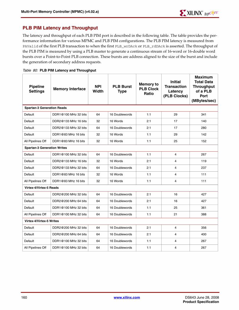
Multi-Port Memory Controller (MPMC) (v4.02.a)
PLB PIM Latency and Throughput
The latency and throughput of each PLB PIM port is described in the following table. The table provides the per-formance information for various MPMC and PLB PIM configurations. The PLB PIM latency is measured from PAValid of the first PLB transaction to when the first PLB_wrDAck or PLB_rdDAck is asserted. The throughput of the PLB PIM is measured by using a PLB master to generate a continuous stream of 16-word or 16-double word bursts over a Point-to-Point PLB connection. These bursts are address aligned to the size of the burst and include the generation of secondary address requests.
Table 80: PLB PIM Latency and Throughput
Pipeline Settings
Memory InterfaceNPI
WidthPLB Burst
Type
Memory to PLB Clock
Ratio
Initial Transaction
Latency (PLB Clocks)
Maximum Total Data
Throughput of a PLB
Port (MBytes/sec)
Spartan-3 Generation Reads
Default DDR1@100 MHz 32 bits 64 16 Doublewords 1:1 29 341
Default DDR2@133 MHz 16 bits 32 16 Words 2:1 17 140
Default DDR2@133 MHz 32 bits 64 16 Doublewords 2:1 17 280
Default DDR1@83 MHz 16 bits 32 16 Words 1:1 29 142
All Pipelines Off DDR1@83 MHz 16 bits 32 16 Words 1:1 25 152
Spartan-3 Generation Writes
Default DDR1@100 MHz 32 bits 64 16 Doublewords 1:1 4 267
Default DDR2@133 MHz 16 bits 32 16 Words 2:1 4 119
Default DDR2@133 MHz 32 bits 64 16 Doublewords 2:1 4 237
Default DDR1@83 MHz 16 bits 32 16 Words 1:1 4 111
All Pipelines Off DDR1@83 MHz 16 bits 32 16 Words 1:1 4 111
Virtex-4/Virtex-5 Reads
Default DDR2@200 MHz 32 bits 64 16 Doublewords 2:1 16 427
Default DDR2@200 MHz 64 bits 64 16 Doublewords 2:1 16 427
Default DDR1@100 MHz 32 bits 64 16 Doublewords 1:1 25 361
All Pipelines Off DDR1@100 MHz 32 bits 64 16 Doublewords 1:1 21 388
Virtex-4/Virtex-5 Writes
Default DDR2@200 MHz 32 bits 64 16 Doublewords 2:1 4 356
Default DDR2@200 MHz 64 bits 64 16 Doublewords 2:1 4 400
Default DDR1@100 MHz 32 bits 64 16 Doublewords 1:1 4 267
All Pipelines Off DDR1@100 MHz 32 bits 64 16 Doublewords 1:1 4 267
160 www.xilinx.com DS643 June 28, 2008Product Specification

Multi-Port Memory Controller (MPMC) (v4.02.a)
Notes on PLB PIM Performance
The Table 80 on page 160 describes the maximum throughput of a PLB PIM. The maximum throughput of each PLB PIM is usually less than the available throughput of the MPMC core. Though each PIM is usually not capable of fully utilizing the available bandwidth, the remaining MPMC Core/NPI bandwidth is available for other ports to use.
For example, take a six port MPMC with 64-bit DDR2 memory at 200 MHz. This MPMC is capable of 2226 MBytes/sec of theoretical read throughput. In that configuration a single PLB PIM is capable of 427 MBytes/sec of throughput. Therefore:
• Four PLB ports, each running at maximum throughput, could achieve a combined system throughput of up to 1708 MBytes/sec (limited by the PLB PIMs).
• Five PLB ports, each running at maximum throughput, could achieve a combined system throughput of up to 2135 MBytes/sec (limited by the PLB PIMs).
• Six PLB ports, each running at maximum throughput, could achieve a combined system throughput of up to 2226 MBytes/sec (limited by the MPMC Core).
The PLB PIM throughput is most efficient when the PLB burst address range fits within MPMC 16-word (32 bit NPI) and 32-word (64 bit NPI) burst boundaries. The above table assumes the bursts are aligned to the burst size.
XCL PIM Latency and Throughput
The latency and throughput for the XCL PIM port is described in the following table. The table provides perfor-mance information for common MPMC and XCL PIM configurations. The XCL PIM latency is measured from the first push of data into the access FIFO until the first data is available on the read data FIFO. The throughput trans-actions were measured by transferring 1 kilobyte of data in simulation. The time between the first transaction and the last data item is used to divide the number of bytes transferred to calculate the read throughput. The time mea-sured between the first transaction and the last transaction has been sent over the access FIFO is used for the write throughput calculation.
Table 81: XCL PIM Latency and Throughput
Pipeline Settings
Memory Interface LinesizePort
Subtype
Memory to XCL Clock Ratio
Initial Transaction
Latency (Memory Clocks)
Maximum Total Data
Throughput of XCL Port
(MBytes/sec)
Spartan-3 Generation Reads
Default DDR2 @ 133 MHz 32 bits 16 XCL 2:1 17 122
Default DDR2 @ 133 MHz 16 bits 16 XCL 2:1 17 121
Default DDR1 @ 83 MHz 16 bits 8 XCL 1:1 29 70
Default DDR1 @ 83 MHz 16 bits 4 DXCL 1:1 29 40
None DDR1 @ 83 MHz 16 bits 4 DXCL 1:1 23 48
Spartan-3 Generation Writes
Default DDR2 @ 133 MHz 32 bits 16 XCL 2:1 N/A 180
Default DDR2 @ 133 MHz 16 bits 16 XCL 2:1 N/A 178
Default DDR1 @ 83 MHz 16 bits 8 XCL 1:1 N/A 151
Default DDR1 @ 83 MHz 16 bits 1 DXCL 1:1 N/A 35
None DDR1 @ 83 MHz 16 bits 1 DXCL 1:1 N/A 35
161 www.xilinx.com DS643 June 28, 2008Product Specification

Multi-Port Memory Controller (MPMC) (v4.02.a)
Using MPMC in Standalone SystemsYou can use the MPMC core in a processor system that is not derived from the Embedded Development Toolkit (EDK).
Using EDK XPS to Manage the MPMC Core
To use the MPMC in a non-EDK processor system use EDK XPS to manage the MPMC core.
1. Create a design using the Base System Builder (BSB) wizard, choosing a development board that uses the same memory technology to be used in the actual design, with all other cores removed except for the SDRAM memory controller.
2. Double-click on the MPMC instance in the System Assembly view to configure MPMC using the MPMC interface. Parameterize the MPMC as needed, including choosing the desired PIMs.a. Remove all unwanted peripherals and processors. b. In the XPS Port tab, delete any external I/O associated with the removed peripherals, and connect all
relevant PIM signals as external I/O.
Choose Filters >All port filter to show all MPMC ports. Each PIM I/O signal has a port number and PIM type in the interface which corresponds to the port order and PIM type shown in the MPMC GUI.
3. Run Hardware >Generate Netlist to check for any incorrect, missing, or extraneous connections; correct as needed.
4. Add the XPS file as a source to the ISE project using Project > Add Source and build. For an example instantiation template, see the system_stub.vhd file in the EDK project hdl/ directory.
Virtex-4/Virtex-5 Reads
Default DDR2 @ 200 MHz 32 bits 16 XCL 2:1 16 188
Default DDR2 @ 200 MHz 16 bits 16 XCL 2:1 16 188
Default DDR2 @ 200 MHz 16 bits 8 XCL 2:1 16 133
Default DDR1 @ 100 MHz 16 bits 4 DXCL 1:1 26 54
None DDR1 @ 100 MHz 16 bits 4 DXCL 1:1 20 65
Virtex-4/Virtex-5 Writes
Default DDR2 @ 200 MHz 32 bits 16 XCL 2:1 N/A 268
Default DDR2 @ 200 MHz 16 bits 16 XCL 2:1 N/A 265
Default DDR2 @ 200 MHz 16 bits 8 XCL 2:1 N/A 223
Default DDR1 @ 100 MHz 16 bits 1 DXCL 1:1 N/A 42
None DDR1 @ 100 MHz 16 bits 1 DXCL 1:1 N/A 42
Table 81: XCL PIM Latency and Throughput (Continued)
Pipeline Settings
Memory Interface LinesizePort
Subtype
Memory to XCL Clock Ratio
Initial Transaction
Latency (Memory Clocks)
Maximum Total Data
Throughput of XCL Port
(MBytes/sec)
162 www.xilinx.com DS643 June 28, 2008Product Specification

Multi-Port Memory Controller (MPMC) (v4.02.a)
DS643 JuneProduct Sp
Reference Documents• http://www.xilinx.com/ise/embedded/edk_docs.htm
• ISE documentation page: http://www.xilinx.com/ise/logic_design_prod/foundation.htm
• Memory website contains links to the following documents:
- Memory Interfaces Data Capture Using Direct Clocking Technique
- MIG User Guide, which provides additional MIG information and documentationhttp://www.xilinx.com/products/design_resources/mem_corner
• MicroBlaze Processor Reference Guidehttp://www.xilinx.com/ise/embedded_design_prod/index.htm
• Spartan-3 generation FPGAs page:http://www.xilinx.com/products/silicon_solutions/fpgas/spartan_series/index.htm
• Virtex-4 page: http://www.xilinx.com/products/silicon_solutions/fpgas/virtex/virtex4/index.htm
• Virtex-5 page: http://www.xilinx.com/products/silicon_solutions/fpgas/virtex/virtex5/index.htm
• Virtex-5 FPGAs Reference Guide<EDK Install Directory>/doc/usenglish/embedproc_ug200.pdf
• Specification for PLB v4.6 Bus Protocol with Xilinx Simplifications, SP026, <EDK Install Directory>/doc/usenglish/sp026.pdf
• PLB v3.4 and OPB to PLB v4.6 System and Core Migration User Guide:<EDK Install Directory>/doc/usenglish/mg_ug.pdf
• Application Note: XAPP768C, Interfacing Spartan-3 Devices With 166 MHz or 333 Mb/s DDR SDRAM Memories: http://www.xilinx.com/support/software/memory/protected/XAPP768c.pdf
• Application Note: XAPP454, DDR2 SDRAM Memory Interface for Spartan-3 FPGAs:http://www.xilinx.com/bvdocs/appnotes/xapp454.pdf
• Design resources page: http://www.xilinx.com/products/design_resources/proc_central/index.htm
• Development boards page: http://www.xilinx.com/products/devboards/index.htm
• IBM CoreConnect documentation website contains the following documents:CoreConnect Device Control Register Bus: Architecture Specification:IBMCoreConnect 64-Bit Processor Local Bus: Architecture Specification:IBM CoreConnect 64-Bit On-Chip Peripheral Bus: Architectural Specificationhttp://www.xilinx.com/products/ipcenter/dr_pcentral_coreconnect.htm
• LocalLink User Interface page:http://www.xilinx.com/aurora/aurora_protocol_member/sp006.pdf
• Video Starter Kit: http://www.xilinx.com/vsk_v3
• Rainier Processor Memory Interface Block Micro Architecture Specification Version 0.82
• Answer Records (Contains useful design, debug, and implementation):http://www.xilinx.com/xlnx/xil_ans_browser.jsp
• Answer Records with MPMC content clarification and examples:
- On MHS signal and MHS external port name matching: http://www.xilinx.com/support/answers/14264.htm
- On using MPMC as a Standalone Core: http://www.xilinx.com/support/answers/29732.htm
- On using the Native Port Interface: http://www.xilinx.com/support/answers/24912.htm
28, 2008 www.xilinx.com 163ecification

Multi-Port Memory Controller (MPMC) (v4.02.a)
164
Revision History The following table shows the revision history for this document.
Date Version Revision
09/26/07 3.00.a Initial release in 9.2i
11/8/07 3.00.B Service Pack 1 update
01/11/08 4.00.a Major release for 10.1
03/12/08 4.01.a Service Pack 1 update
06/28/08 4.02.a Service Pack 2 update
www.xilinx.com DS643 June 28, 2008Product Specification