dhananjayparkar.files.wordpress.com · Web viewSEMICONDUCTOR ELECTRONICS: MATERIALS, DEVICES AND...
20
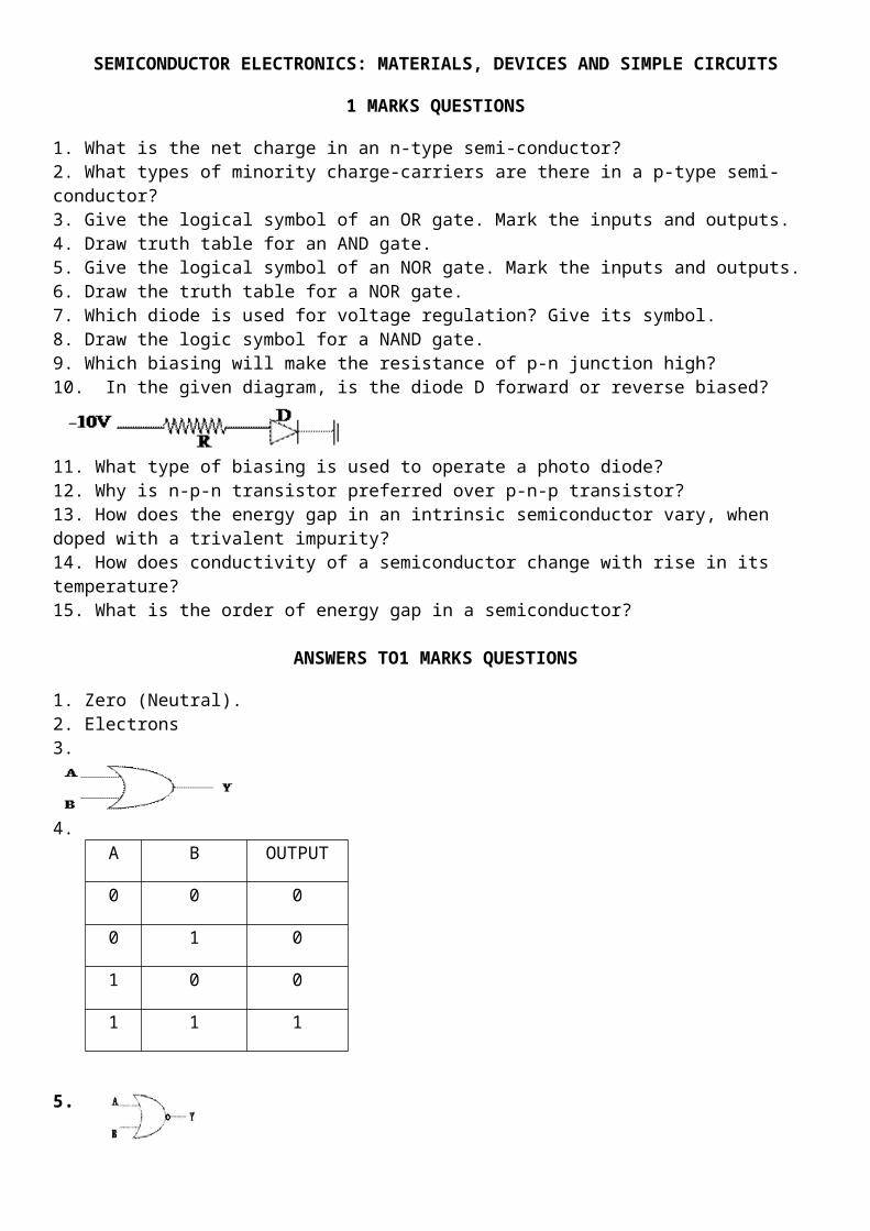
SEMICONDUCTOR ELECTRONICS: MATERIALS, DEVICES AND SIMPLE CIRCUITS 1 MARKS QUESTIONS 1. What is the net charge in an n-type semi-conductor? 2. What types of minority charge-carriers are there in a p-type semi- conductor? 3. Give the logical symbol of an OR gate. Mark the inputs and outputs. 4. Draw truth table for an AND gate. 5. Give the logical symbol of an NOR gate. Mark the inputs and outputs. 6. Draw the truth table for a NOR gate. 7. Which diode is used for voltage regulation? Give its symbol. 8. Draw the logic symbol for a NAND gate. 9. Which biasing will make the resistance of p-n junction high? 10. In the given diagram, is the diode D forward or reverse biased? 11. What type of biasing is used to operate a photo diode? 12. Why is n-p-n transistor preferred over p-n-p transistor? 13. How does the energy gap in an intrinsic semiconductor vary, when doped with a trivalent impurity? 14. How does conductivity of a semiconductor change with rise in its temperature? 15. What is the order of energy gap in a semiconductor? ANSWERS TO1 MARKS QUESTIONS 1. Zero (Neutral). 2. Electrons 3. 4. 5. A B OUTPUT 0 0 0 0 1 0 1 0 0 1 1 1
Transcript of dhananjayparkar.files.wordpress.com · Web viewSEMICONDUCTOR ELECTRONICS: MATERIALS, DEVICES AND...
SEMICONDUCTOR ELECTRONICS: MATERIALS, DEVICES AND SIMPLE CIRCUITS
1 MARKS QUESTIONS
1. What is the net charge in an n-type semi-conductor?2. What types of minority charge-carriers are there in a p-type semi-conductor?3. Give the logical symbol of an OR gate. Mark the inputs and outputs.4. Draw truth table for an AND gate.5. Give the logical symbol of an NOR gate. Mark the inputs and outputs.6. Draw the truth table for a NOR gate.7. Which diode is used for voltage regulation? Give its symbol.8. Draw the logic symbol for a NAND gate.9. Which biasing will make the resistance of p-n junction high?10. In the given diagram, is the diode D forward or reverse biased?
11. What type of biasing is used to operate a photo diode?12. Why is n-p-n transistor preferred over p-n-p transistor?13. How does the energy gap in an intrinsic semiconductor vary, when doped with a trivalent impurity?14. How does conductivity of a semiconductor change with rise in its temperature?15. What is the order of energy gap in a semiconductor?
ANSWERS TO1 MARKS QUESTIONS
1. Zero (Neutral).2. Electrons3.
4.
5.
A , B are inputs and Y output.6.
A B OUTPUT
0 0 0
0 1 0
1 0 0
1 1 1
A B OUTPUT
0 0 1
1 0 0
0 1 0
1 1 0
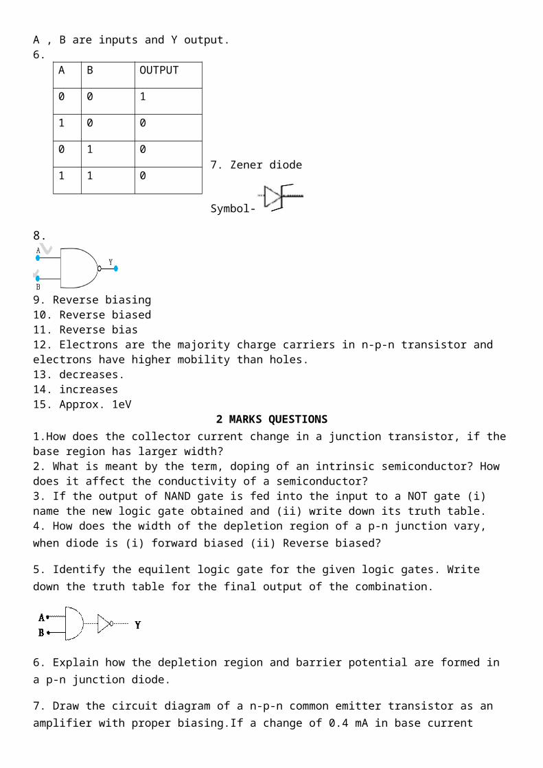
7. Zener diode
Symbol-
8.
9. Reverse biasing10. Reverse biased11. Reverse bias12. Electrons are the majority charge carriers in n-p-n transistor and electrons have higher mobility than holes.13. decreases.14. increases15. Approx. 1eV
2 MARKS QUESTIONS1.How does the collector current change in a junction transistor, if the base region has larger width?2. What is meant by the term, doping of an intrinsic semiconductor? How does it affect the conductivity of a semiconductor?3. If the output of NAND gate is fed into the input to a NOT gate (i) name the new logic gate obtained and (ii) write down its truth table.4. How does the width of the depletion region of a p-n junction vary, when diode is (i) forward biased (ii) Reverse biased?
5. Identify the equilent logic gate for the given logic gates. Write down the truth table for the final output of the combination.
6. Explain how the depletion region and barrier potential are formed in a p-n junction diode.
7. Draw the circuit diagram of a n-p-n common emitter transistor as an amplifier with proper biasing.If a change of 0.4 mA in base current causes a change of 10mA in collector current in a common emitter amplifier, find a.c.current gain of the transistor.
ANSWERS TO2 MARKS QUESTIONS
1. Ans- As we knowIf we increase base width region there is more recombination in the base region. So base current(Ib) will increase. Hence, the collector current decreases if emitter current (Ie) is fixed for a transistor.2. Adding impurities-trivalent or pentavalent, conductivity increases3. AND gate.
A B OUTPUT0 0 01 0 00 1 01 1 1
4.(i) decreases (ii) increases:-
5. NAND gate
Truth table
5.
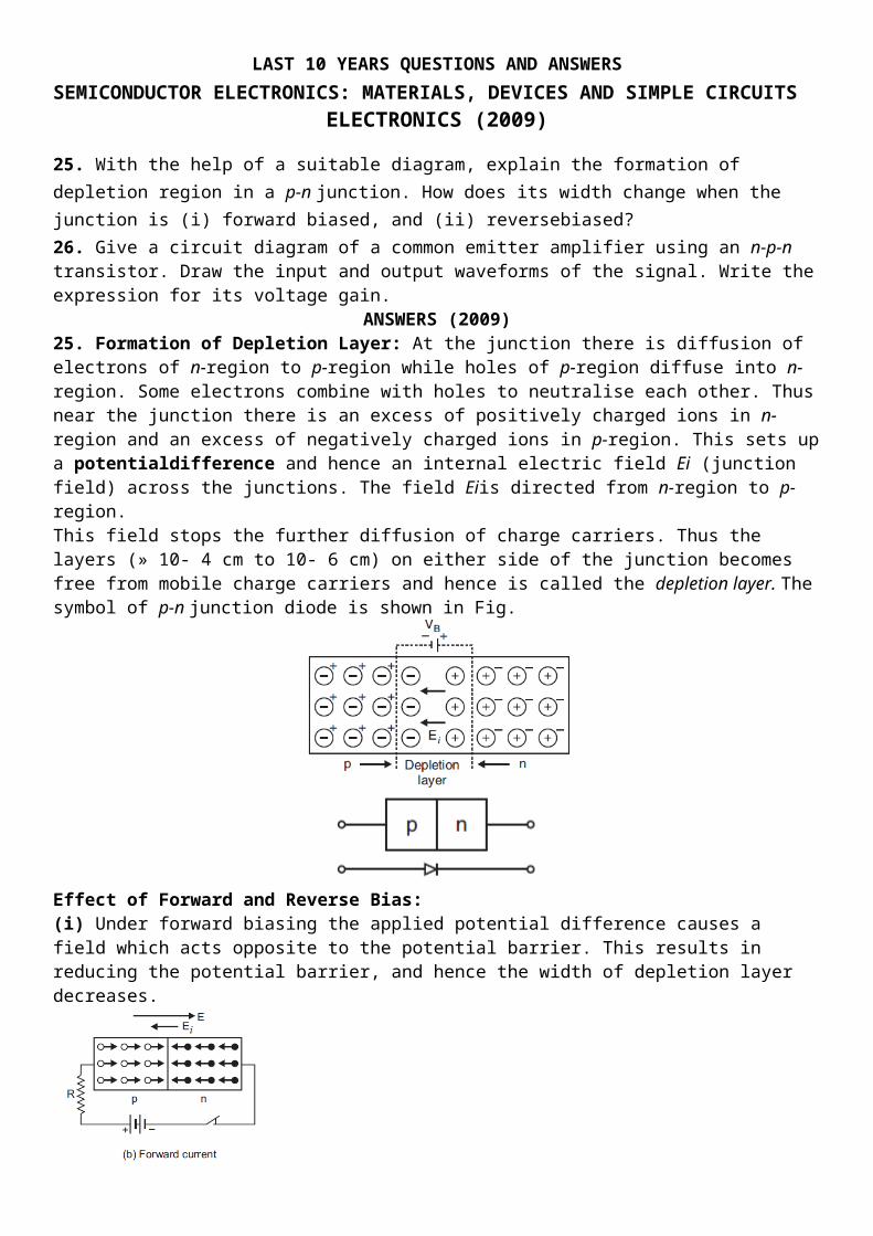
6.Formation of Depletion Layer: At the junction there is diffusion of electrons of n-region to p-region while holes of p-region diffuse into n-region. Some electrons combine with holes to neutralise each other. Thus near the junction there is an excess of positively charged ions in n-region and an excess of negatively charged ions in p-region. This sets up a potentialdifference and hence an internal electric field Ei (junction field) across the junctions. The field Eiis directed from n-region to p-region.
7. ß= change in collector current/change in base current = 25
3 MARKS QUESTIONS1. Draw energy band diagram for a (i) p- type extrinsic semiconductor (ii) n-type extrinsic semiconductor (iii) intrinsic semiconductors.2. Define the terms ‘potential barrier’ and ‘depletion region’ for a p-n junction diode. State how the thickness of depletion region will change when the p.n junction diode is (i) forward biased. (ii) Reverse biased.3.With the help of labeled circuit diagram, explain the rectification action of a full wave rectifier.4.Distinguish between conductors, semiconductors and insulators on the basis of band theory of solids.5.Draw the circuit diagram of a common-emitter amplifier, with appropriate biasing. What is the phase difference between the input and output signals? State two reasons why a common-emitter-amplifier is preferred to a common base amplifier?6.With a circuit diagram, briefly explain how a zener diode can be used as a voltage regulator.7.What is an intrinsic semiconductor? How can you convert an intrinsic semiconductor into n-type extrinsic semiconductor?
8. The V-I characteristic of a silicon diode is shown in the Fig. Calculate the resistance of the diode at (a) ID= 15 mA and (b) VD= –10 V.
9. From the output characteristics shown in Fig, calculate the values ofac and dc of the transistor when VCE
is10 V and IC = 4.0 mA.
A B OUTPUT0 0 11 0 10 1 11 1 0

ANSWERS TO3 MARKS QUESTIONS1.(i) p-type semiconductor
(ii) n-type semi-conductor
(iii) Intrinsic semiconductor
2. Potential barrier-The loss of electrons from the n-region and the gain of electron by the p-region cause a difference of potential across the junction of the two regions. Since this potential tends to prevent the movement of electron from the n region into the p region, it is often called a barrier potential.Depletion region- The space-charge region on either side of the junction which is free of electrons and holes is known as depletion region.(i) Thickness of depletion region decreases when diode is forward biased.(ii) Thickness of depletion region increases when diode is reverse biased.3. Answer included in 10 years question answer.4.In metal either the conduction band is partially filled and the balanced band is partially empty or the conduction and valance bands overlap. When there is overlap electrons from valence band can easily move into the conduction band. This situation makes a large number of electrons available for electrical conduction. When the valence band is partially empty, electrons from its lower level can move to higher level making conduction possible

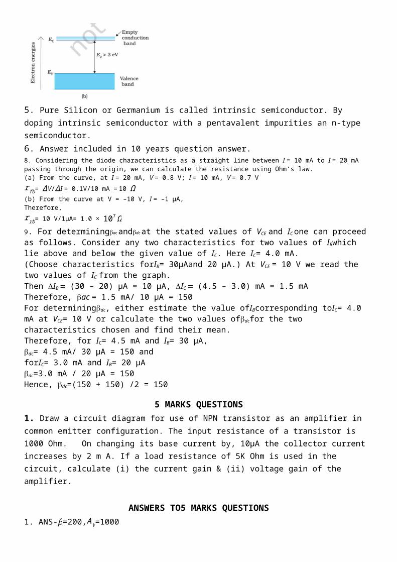
This situation is shown in Fig.(c). Here a finite but small band gap (Eg< 3 eV) exists. Because of the small band gap, at room temperature some electrons from valence band can acquire enough energy to cross the energy gap and enter the conduction band. These electrons (though small in numbers) can move in the conduction band.
In this case, as shown in Fig.(b), a large band gap Egexists (Eg> 3 eV). There are no electrons in the conduction band, and therefore no electrical conduction is possible. Note that the energy gap is so large that electrons cannot be excited from the valence band to the conduction band by thermal excitation. This is the case of insulators.
5. Pure Silicon or Germanium is called intrinsic semiconductor. By doping intrinsic semiconductor with a pentavalent impurities an n-type semiconductor.6. Answer included in 10 years question answer.8. Considering the diode characteristics as a straight line between I = 10 mA to I = 20 mA passing through the origin, we can calculate the resistance using Ohm’s law.(a) From the curve, at I = 20 mA, V = 0.8 V; I = 10 mA, V = 0.7 Vr fb= ∆V/∆I = 0.1V/10 mA = 10 Ω(b) From the curve at V = –10 V, I = –1 μA,Therefore,rrb= 10 V/1μA= 1.0 × 10⁷ Ω9. For determiningac anddc at the stated values of VCE and IC one can proceed as follows. Consider any two characteristics for two values of IBwhich lie above and below the given value of IC. Here IC= 4.0 mA.(Choose characteristics forIB= 30μAand 20 μA.) At VCE = 10 V we read the two values of IC from the graph.Then IB (30 – 20) μA = 10 μA, IC (4.5 – 3.0) mA = 1.5 mATherefore, ac = 1.5 mA/ 10 μA = 150For determiningdc, either estimate the value ofIBcorresponding toIC= 4.0 mA at VCE= 10 V or calculate the two values ofdcfor the two characteristics chosen and find their mean.Therefore, for IC= 4.5 mA and IB= 30 μA,dc= 4.5 mA/ 30 μA = 150 andforIC= 3.0 mA and IB= 20 μAdc=3.0 mA / 20 μA = 150Hence, dc=(150 + 150) /2 = 150
5 MARKS QUESTIONS1. Draw a circuit diagram for use of NPN transistor as an amplifier in common emitter configuration. The input resistance of a transistor is 1000 Ohm. On changing its base current by, 10µA the collector current increases by 2 m A. If a load resistance of 5K Ohm is used in the circuit, calculate (i) the current gain & (ii) voltage gain of the amplifier.
ANSWERS TO5 MARKS QUESTIONS
1. ANS-β=200, AV =1000 LAST 10 YEARS QUESTIONS AND ANSWERS
SEMICONDUCTOR ELECTRONICS: MATERIALS, DEVICES AND SIMPLE CIRCUITS
ELECTRONICS (2009) 25. With the help of a suitable diagram, explain the formation of depletion region in a p-n junction. How does its width change when the junction is (i) forward biased, and (ii) reversebiased?26. Give a circuit diagram of a common emitter amplifier using an n-p-n transistor. Draw the input and output waveforms of the signal. Write the expression for its voltage gain.
ANSWERS (2009)25. Formation of Depletion Layer: At the junction there is diffusion of electrons of n-region to p-region while holes of p-region diffuse into n-region. Some electrons combine with holes to neutralise each other. Thus near the junction there is an excess of positively charged ions in n-region and an excess of negatively charged ions in p-region. This sets up a potentialdifference and hence an internal electric field Ei (junction field) across the junctions. The field Eiis directed from n-region to p-region.This field stops the further diffusion of charge carriers. Thus the layers (» 10- 4 cm to 10- 6 cm) on either side of the junction becomes free from mobile charge carriers and hence is called the depletion layer. The symbol of p-n junction diode is shown in Fig.
Effect of Forward and Reverse Bias:(i) Under forward biasing the applied potential difference causes a field which acts opposite to the potential barrier. This results in reducing the potential barrier, and hence the width of depletion layer decreases.
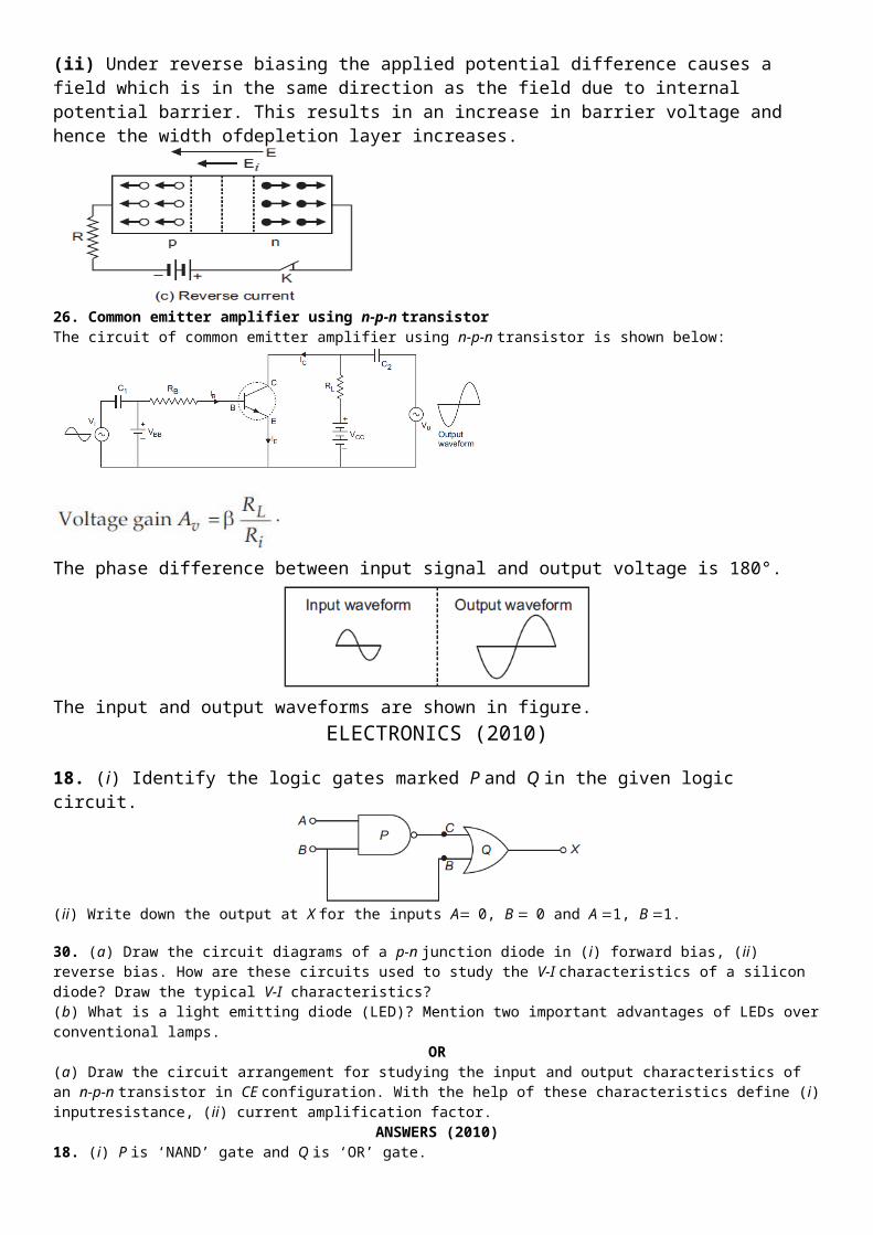
(ii) Under reverse biasing the applied potential difference causes a field which is in the same direction as the field due to internal potential barrier. This results in an increase in barrier voltage and hence the width ofdepletion layer increases.
26. Common emitter amplifier using n-p-n transistorThe circuit of common emitter amplifier using n-p-n transistor is shown below:
The phase difference between input signal and output voltage is 180°.
The input and output waveforms are shown in figure.ELECTRONICS (2010)
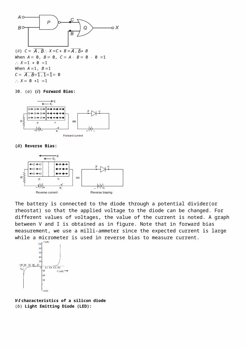
18. (i) Identify the logic gates marked P and Q in the given logic circuit.
(ii) Write down the output at X for the inputs A0, B 0 and A 1, B 1.
30. (a) Draw the circuit diagrams of a p-n junction diode in (i) forward bias, (ii) reverse bias. How are these circuits used to study the V-I characteristics of a silicon diode? Draw the typical V-I characteristics?(b) What is a light emitting diode (LED)? Mention two important advantages of LEDs over conventional lamps.
OR(a) Draw the circuit arrangement for studying the input and output characteristics of an n-p-n transistor in CE configuration. With the help of these characteristics define (i) inputresistance, (ii) current amplification factor.
ANSWERS (2010)18. (i) P is ‘NAND’ gate and Q is ‘OR’ gate.
(ii) C A . BX C B A . BBWhen A 0, B 0, C A B 0 0 1X 1 0 1When A 1, B 1C A . B1.110X 0 1 1
30. (a) (i) Forward Bias:
(ii) Reverse Bias:
The battery is connected to the diode through a potential divider(or rheostat) so that the applied voltage to the diode can be changed. For different values of voltages, the value of the current is noted. A graph between V and I is obtained as in figure. Note that in forward bias measurement, we use a milli-ammeter since the expected current is large while a micrometer is used in reverse bias to measure current.
V-I characteristics of a silicon diode(b) Light Emitting Diode (LED):
A light emitting diode is simply a forward biased p-n junction which emits spontaneous light radiation. When forward bias is applied, the electron and holes at the junction recombine and energy released is emitted in the form of light. For visible radiation phosphorus doped GaAs is commonly used.The advantages of LEDs are:(i) Low operational voltage and less power.(ii) Fast action with no warm up time.(iii) Emitted light is nearly monochromatic radiation.(iv) They have long life.
OR(a) Characteristic Curves: The circuit diagram for determining the static characteristic curvesof an n-p-n transistor in common-emitter configuration is shown in figure.
Common Emitter Characteristics:(i)Input characteristics: These characteristic curves are obtained by plotting base current (IB) versus base-emitter voltage VBEfor fixed collector-emitter voltage VCE. Fig. represents these characteristics.
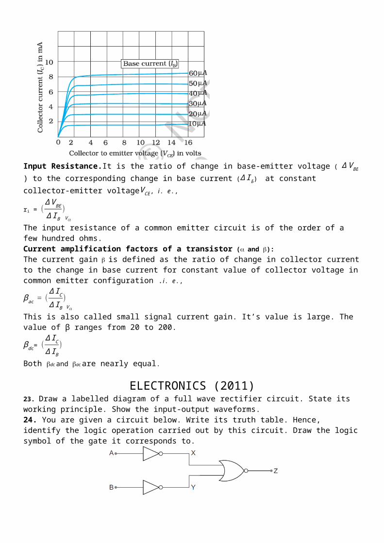
(ii) Output characteristics: These characteristics areobtained by plotting collector current ICversus collector-emitter voltage VCEat a fixed value of base current IB. The base current is changed to some other fixed value and the observations of ICversus VCEare repeated. Fig. represents the output characteristics of a common-emitter circuit.
Input Resistance.It is the ratio of change in base-emitter voltage ( ∆ V BE) to the corresponding change in base current (∆ I B) at constant collector-emitter voltageV CE, i. e.,
ri = (∆ V BE
∆ I B)
V CE
The input resistance of a common emitter circuit is of the order of a few hundred ohms.Current amplification factors of a transistor (and ):The current gain is defined as the ratio of change in collector current to the change in base current for constant value of collector voltage in common emitter configuration .i. e.,
βac(∆ I C
∆ I B)
V CE
This is also called small signal current gain. It’s value is large. The value of β ranges from 20 to 200.
βdc= (∆ I C
∆ I B)
Both dc and ac are nearly equal.

ELECTRONICS (2011)23. Draw a labelled diagram of a full wave rectifier circuit. State its working principle. Show the input-output waveforms.24. You are given a circuit below. Write its truth table. Hence, identify the logic operation carried out by this circuit. Draw the logic symbol of the gate it corresponds to.
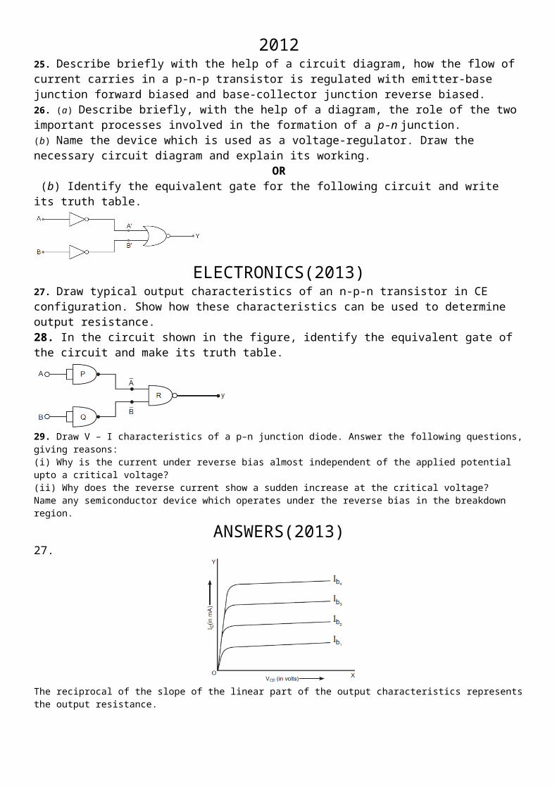
201225. Describe briefly with the help of a circuit diagram, how the flow of current carries in a p-n-p transistor is regulated with emitter-base junction forward biased and base-collector junction reverse biased.26. (a) Describe briefly, with the help of a diagram, the role of the two important processes involved in the formation of a p-n junction.(b) Name the device which is used as a voltage-regulator. Draw the necessary circuit diagram and explain its working.
OR (b) Identify the equivalent gate for the following circuit and write its truth table.
ELECTRONICS(2013)27. Draw typical output characteristics of an n-p-n transistor in CE configuration. Show how these characteristics can be used to determine output resistance.28. In the circuit shown in the figure, identify the equivalent gate of the circuit and make its truth table.
29. Draw V – I characteristics of a p–n junction diode. Answer the following questions, giving reasons:(i) Why is the current under reverse bias almost independent of the applied potential upto a critical voltage?(ii) Why does the reverse current show a sudden increase at the critical voltage?Name any semiconductor device which operates under the reverse bias in the breakdown region.
ANSWERS(2013)27.
The reciprocal of the slope of the linear part of the output characteristics represents the output resistance.
ro=(∆ V CE
∆ I C¿¿ Ib4
(as shown in fig.)28.
Gates, P, Q and R act as NOT, NOT and NAND gates respectively.So y A . BA BThe combination acts as OR Gate.Truth Table of the combination
Truth Table of OR Gate
21. (i)
In the reverse biasing, the current of order of A is due to movement/drifting of minority charge carriers from one region to another through the junction.A small applied voltage is sufficient to sweep the minority charge carriers through the junction. So reverse current is almost independent of critical voltage.(ii) At critical voltage (or breakdown voltage), a large number of covalent bonds break, resulting in the increase of large number of charge carriers. Hence, current increases at critical voltage.Semiconductor device that is used in reverse biasing is zener diode.
ELECTRONICS(2014)31. Explain, with the help of a circuit diagram, the working of a p-n junction diode as a half-wave rectifier.32. Draw a circuit diagram of n-p-n transistor amplifier in CE configuration. Under what condition does the transistor act as an amplifier?
ANSWERS (2014)31.
Working(i) During positive half cycle of input alternating voltage, the diode is forward biased and a current flows through the load resistor RL, and we get an output voltage.(ii) During other negative half cycle of the input alternating voltage, the diode is reverse biased and it does not conduct (under break down region).Hence AC voltage can be rectified in the pulsating and unidirectional voltage.32. A circuit diagram of n–p–n transistor as an amplifier is shown in figure.
Condition:The base-emitter junction of the transistor must be forward biased and the collector-emitter junction must be reverse biased.
ELECTRONICS (2015)18. Write two important considerations used while fabricating a Zener diode. Explain, with the help of a circuit diagram, the principle and working of a Zener diode as voltage regulator.
19. Draw the necessary energy band diagrams to distinguish between conductors, semiconductors and insulators. How does the change in temperature affect the behaviour of these materials? Explain briefly.
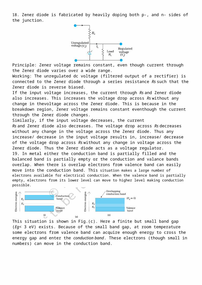
ANSWERS (2015)18. Zener diode is fabricated by heavily doping both p-, and n- sides of the junction.
Principle: Zener voltage remains constant, even though current through the Zener diode varies over a wide range.Working: The unregulated dc voltage (filtered output of a rectifier) is connected to the Zener diode through a series resistance Rs such that the Zener diode is reverse biased.If the input voltage increases, the current through Rs and Zener diode also increases. This increases the voltage drop across Rs without any change in thevoltage across the Zener diode. This is because in the breakdown region, Zener voltage remains constant eventhough the current through the Zener diode changes.Similarly, if the input voltage decreases, the currentRs and Zener diode also decreases. The voltage drop across Rs decreases without any change in the voltage across the Zener diode. Thus any increase/ decrease in the input voltage results in, increase/ decrease of

the voltage drop across Rs without any change in voltage across the Zener diode. Thus the Zener diode acts as a voltage regulator.19. In metal either the conduction band is partially filled and the balanced band is partially empty or the conduction and valance bands overlap. When there is overlap electrons from valence band can easily move into the conduction band. This situation makes a large number of electrons available for electrical conduction. When the valence band is partially empty, electrons from its lower level can move to higher level making conduction possible.
This situation is shown in Fig.(c). Here a finite but small band gap (Eg< 3 eV) exists. Because of the small band gap, at room temperature some electrons from valence band can acquire enough energy to cross the energy gap and enter the conduction band. These electrons (though small in numbers) can move in the conduction band.
In this case, as shown in Fig.(b), a large band gap Eg exists (Eg> 3 eV). There are no electrons in the conduction band, and therefore no electrical conduction is possible. Note that the energy gap is so large that electrons cannot be excited from the valence band to the conduction band by thermal excitation. This is the case of insulators.
20164. Name the logic gates marked P and Q in the given logic circuit.
18. Draw the circuit diagram of a common emitter amplifier using n-p-n transistor. Derive an expression for the current gain βac.
ANSWERS (2016)4. (i) P = NOT gate (ii) Q = OR gate

18.(a)
(b)
ELECTRONICS(2017)13. (a) In the following diagram, is the junction diode forward biased or reverse biased ?
(b) Draw the circuit diagram of a full wave rectifier and state how it works. (3)19. (a) Write the functions of the three segments of a transistor.(b) The figure shows the input waveforms A and B for ‘AND’ gate.
Draw the output waveform and write the truth table for this logic gate. (3)ANSWERS (2017)
13. a) Reverse Biasedb) Diagram of full wave rectifier
Working: The diode D1 is forward biased during one half cycle and current flows through the resistor, but diode D2 is reverse biased and no current flows through it. During the other half of the signal, D1 gets reverse biased and no current passes through it, D2 gets forward biased and current flows through it. In both half cycles current, through the resistor, flows in the same direction.
19. (a) Emitter: Supplies a large number of majority charge carriers.Base: Controls the flow of majority carriers from the emitter to the collector.Collector: It collects the majority carriers from the base / majority of those emitted by the emitter.
(b)
TRUTH TABLE (AND GATE)A B Y
0 0 0
0 1 0
1 0 0
1 1 1
201811. Draw the typical input and output characteristics of an n-p-n transistor in CE configuration. Show how these characteristics can be used to determine (a) the input resistance (r i) and (b) current amplification factor (β ¿12. (a) A student wants to use two p-n junction diodes to convert alternating current into direct current. Draw the labelled circuit diagram she would use and explain how it works.(b) Give the truth table and circuit symbol for NAND gate.
ANSWER (2018)11. Input characteristics of an n-p-n transistor in CE configuration.
Output characteristics of an n-p-n transistor in CE configuration

Input Resistance.It is the ratio of change in base-emitter voltage ( ∆ V BE) to the corresponding change in base current (∆ I B) at constant collector-emitter voltage V CE, i. e.,
ri = (∆ V BE
∆ I B)
V CE
The input resistance of a common emitter circuit is of the order of a few hundred ohms.Current amplification factors of a transistor (and ):The current gain β is defined as the ratio of change in collector current to the change in base current for constant value of collector voltage in common emitter configuration i. e.,
βac(∆ I C
∆ I B)
V CE
This is also called small signal current gain. It’s value is large.The value of ranges from 20 to 200.
βdc= (∆ I C
∆ I B)
Both dc and ac are nearly equal.12. (a) Full wave rectifier circuit.
Suppose the input voltage to A with respect to the centre tap at any instant is positive. At that instant, voltage at B will be negative as shown in Fig. So, diode D1 gets forward biased and conducts (while D2 being reverse biased is not conducting). Hence, during this positive half cycle we get an output current (and a output voltage across the load resistor RL) as shown in Fig. In the course of the ac cycle when the voltage at A becomes negative with respect to centre tap, the voltage at B would be positive. In this part of the cycle diodeD1 would not conduct but diode D2 would, giving an output current and output voltage (across RL) during the negative half cycle of the input ac. Thus, we get output voltage during both the positive as well as the negative half of the cycle.
(b) Truth table of NAND gateA B Y0 0 10 1 11 0 11 1 0