. ATARI® - exxoshost.co.uk · 1.0 2.0 VCX SERIES MONITORS SCOPE This document describes a monitor...
28
.... , ... · Jl\. ATARI® SMI94 , . .. ,, . .... •. <" Technical Manual ·' · Februari I 99 I
-
Upload
hoangquynh -
Category
Documents
-
view
213 -
download
0
Transcript of . ATARI® - exxoshost.co.uk · 1.0 2.0 VCX SERIES MONITORS SCOPE This document describes a monitor...
.... , ... ·
Jl\. ATARI®
SMI94
, ... ,, .!~ .
.... •. <"
Technical Manual
·'· Februari I 99 I
/ ·-··"!
- ~-.
)
TABLE OF CONTENTS
Subject
Scope ..................................... . General Description ......••.•.••••..•.... ~. Electrical Characteristics .....•........... Display Performance ............••.......... controls .................................. . Options ................................... . Mechanical Description ...•.•.••.••......... Environmental Performance ••.•••••••••...... Agency Compliance ......................... . Interface ••••••.• ~ .•......••••.•........... Theory of Operation ..•..••..•.•••..•....... Appendix: Figures Block Diagram Trouble Shooting Chart Schematics
Section
1 2 3 4 5 6 7 8 9
10 11

--.....__
)
1.0
2.0
VCX SERIES MONITORS
SCOPE
This document describes a monitor series that covers a range of horizontal scan frequencies and includes options to satisfy requirements in a wide variety of applications.
GENERAL DESCRIPTION
The monitor series is supplied with a 20-inch diagonal tube with a 114 degree deflection. ( 15" 1 17" and 2 4" CRT' s are available.)
The monitor can be custom configured for any horizontal scan frequency from 32 KHz to 128 KHz 1 and for vertical field frequencies from 49 Hz to 120 Hz.
The specific values included in this document are for a typical monitor operating at a 66 KHz horizontal scan rate. Other scan rate information can be obtained by consulting OEM sales or application engineering.
3.0 ELECTRICAL CHARACTERISTICS
3.1 Power Supply:
Input Voltage Power Frequency Power Inrush Current
90 to 137 VAC or 180 to 264 VAC 47-63 Hz 64 Watts 40 Amps peak at 120 VAC 60 Amps peak at 220 VAC
3
,~.
4.5 Image Distortion:
4.5.1
I __., fool-
g
.. ~
\
PINCUSHION AND BARREL:
Input Image
,_
I e
c
f b
I ~ A
.A
-~
..... I . a
A rectangle outlining the video perimeter
~ h
[+-
d
v -Pincushion or Barrel: a through h
0.07" max Incremental Pincushion: 0.085 11 max within 2"
0.045" max within 1"
4.5.2 Parallelogram: Input image
a
A rectangle outlining the video perimeter
Diagonals (a , b) are within 2%
6

-)
/
4.5.3 Trapezoid: Input image a rectangle outlining the
video perimeter
~~r~--~~~~~=======~1l=bt!~~~ ~
.&. I
Distances a through d 0.14 inches max
4.5.4 Rotation: Input image
A
a rectangle outlining the video perimeter.
a
A - B = 0.07 inches max
4.5.5 center Bow:
0.07 inches max
7

)
. ) ,. /
4.5.6 Linearity:
0
D
0 D 0 D 0
0 -
0
Using the above pattern, the linearity shall be better than 7% vertically and better that 9% horizontally.
4.6 Resolution: 1300 Lines min. at 10 Ft-L P104 phosphor and standard 48% Transmission glass
4.7 Light Output: 30 Ft-L min. with max settings
4.8 Display Stability:
4.8.1
4.8.2
Jitter:
resulting from Monitor Radiated power line inch max. , down to a
Jitter and swim Generated Sources: interference of o. 005 frequency of 47 Hz.
Interference from other nonsynchronous sources shall not produce more than 0. 003 inches of jitter on the display.
TUrn on Drift:
After a 10 minute warm-up, the periphery of the display shall not drift more than 0.10 inches in any direction. During the 10 minute warm-up, the display shall not "wrap around 11 the raster •
8

-) /
4.8.3 High Voltage Regulation:
With an all white active display-, dimensions shall not change by more than o. 5%, when going from 2 Ft-L to 30 Ft-L light output (ref. P104 phosphor).
4.8.4 Black Level Stability:
When changing the data pattern from 5% Average Picture Level (APL) to 100% APL, the reference black level will stay constant with 2%.
5.0 CONTROLS
5.1 User:
Brightness Power switch Contrast (Available on Grey Scale Units)
5.2 Internal:
Contrast Brightness Horizontal Centering (Phase) Horizontal Size Horizontal Linearity Vertical Size Vertical Linearity G2 Bias static Focus Vertical Dynamic Focus Horizontal Dynamic Focus
6.0 OPTIONS
6.1 Video:
TTL 1 to 3 Bits ECL 1 to 3 Bits Analog Composite Video, RS343A
6.2 Phosphors:
P104 standard All phosphors available as options
9

j /
)
6.3
6.4
Anti-Reflection Treatment:
Fine Etch or Polished is standard Bonded quarter wavelength optical coated panel available as options
orientation Format:
Landscape and portrait with horizontal scan in Long or Short dimension
6.5 Controls:
Remote contrast LED Power indicator
6.6 Power:
ECL Supply: -lO.OVDC nominal @ 500 rna
10

:. 0
7.0 MECHANICAL DESCRIPTION OF OPTIONAL CABINET WITH TILT-SWIVEL BASE:
Overall Height Overall Width overall Depth Rear Panel Dimensions Weight
8.0 ENVIRONMENTAL PERFORMANCE
14.5 11
17.8 11
15~0 11
13.0 X 9.5 11
36 Lbs.
(368mm) (452mm) (381mm) (330 x 241mm) (16.4 Kilograms)
Operating Temperature (in box) Storage Temperature
5 to 55 degrees c -40 to 65 degrees c
Humidity Operating Altitude Nonoperating Altitude
Vibration:
5% to 95% noncondensing 10,000 Ft. max. 40,000 Ft. max.
Sweep 5-500-5Hz: 0.5g max from 0 to 200 Hz, 0.33g max from 200 to 500 Hz. Duration of sweep is 15 minutes; then 15 minute dwell on peak resonant at 0.55g.
Shock:
20g vertically, longitudinally and laterally, half-sine wave with pulse width 11-15mSec.
9.0 AGENCY COMPLIANCE
The unit is designed to meet the following requirements:
UL478 Fourth Edition Listed/Recognized
CSA C22.2 No. 154
IEC 380, VDE 0806 GS Mark, and VDE 0871 Class B in cabinet
DHHS 21 CFR, Subchapter J, X-Ray Certified
FCC Class B, Part 15 in cabinet
11

I )
10.0 INTERFACE
1. 2. 3. 4. 5. 6. 7. 8. 9.
NOTE:
AC Power In:
10.1 Input Signals:
CEE-22 Receptacle or AC Safety Interlock
Connector: 9 Pin Subminiature D
Typical Pin Assignments
ECL Video ECL Video Return (GND) H Sync v sync N/C ECL (Not) Video ECL (Not) Video Return (GND) Sync Return (GND) N/C
TTL Video N/C H Sync V Sync N/C TTL Video Return (GND) H Sync Return (GND) V Sync Return (GND) N/C
Other Pin Assignments readily accommodated.
10.2 Analog Input:
Analog Input: BNC - RS343A Levels
12

... -) 11.0 THEORY OF OPERATION
11.1 Deflection Board The deflection board does sever~l tasks;
i) processes sync ii) provides horizontal yoke deflection iii)provides vertical yoke deflection iv) provides a sync pulse to the power supply v) provides the required focus voltage vi) provides spot burn protection
i. sync Processing
The 74LS221 U4 is a dual non-retriggerable one shot with Schmitt trigger inputs. Noise is reduced by the hysteresis in the inputs and the non-retriggered action. Jumper blocks JR1/JR2 are provided to select the active edge.
The TLC555 U1 is a level triggered timing device used in the same mode as U4.
The leading edge of horizontal sync triggers the one shot U4. The end of time out triggers the TLC5-55 U1. The second delay is needed to delay the signal a full line. The end of time out of U1 triggers Q1 for a duration determined by C18 and R12. The PLL then centers this pulse on flyback. The data centering potentiometer V10 1 should be set to center the video in the raster. The amount and range of delay is set by R37 1 R68 and V10.
Vertical sync is fed through the one shot U1 to get better noise immunity 1 to offer the option of inversion and to allow some delay for interlace requirements.
ii. Horizontal Deflection
The phase locked loop is used to synchronize the horizontal switch to the timing pulses from the computer or signal generator.
The delayed sync from U1 is buffered through Ql with its pulse width set (by R12 and Cl8) and is capacitively coupled to the PLL 1 U2. The sync is fed into pin 3 of the MC1391. This sync pulse determines when U2 (MC1391/PLL) samples the ramp waveform generated by the yoke and available to pin 4 of U2. The ramp waveform is capacitively coupled to U2. If the sampling occurs at different positions on the ramp at pin 4 1 an error voltage is generated at pin 5. The error voltage is connected to pin 7
13
through a low pass filter. Pin 7 is the timing input of U2, therefore the error voltage created by the phase or frequency difference between the flyback and sync signals controls the oscillator. See figure 1 for waveform details.
The free run frequency of U2 is determined by V1, R19 and C7. The duty cycle of U2 is determined by R16 . and R17. The output is pin 1 which determines the drive of the FET Q3. The FET Q3 is normally on until U2 pulls the gate low and shuts off Q3.
The switching of Q3 drives the horizontal output transistor Q7 through a current transformer. When Q3 is turned on, Q7 turns off. The Baker's clamp D23 is an optional component.
On the right hand half of the screen, transistor Q7 is conducting current through the deflection yoke to ground. This current is provided by the "S" correction capacitor(s) C25 (C44), which has a charge approximately equal to the supply voltage. The damper diode D10 allows current to flow from ground through the deflection yoke to C25 giving the left hand half of the screen.
The flyback capacitor(s) C24 (C43), connects the hot side of the yoke to ground. This component determines the size and length of the flyback pulse.
The "S" shaping capacitor(s) C25 (C44) is used to correct linearity since ~he CRT face has a larger radius of curvature than does the deflecting electron beam. The capacitor(s) corrects the outside versus center of screen linearity. There is a DC voltage equal to the supply voltage plus a parabolic voltage with a peak to peak value of 35 to 90 volts depending on the setup. If the value of C25 is reduced this parabola will increase, reducing the size of the outside characters with respect to the center characters.
Left versus right linearity is controlled with the linearity coil L2. This is a saturable coil in the path of the yoke current. Like the size coil, any inductance in series with the yoke will reduce the size of the picture. This saturable coil will change inductance with ampli~u.de and direction of current flow through it. In this case at the start of a trace the linearity coil has an inductance of 20% of the yoke. By the center of the trace, the linearity coil inductance has decreased to about 5% of the yoke where it remains for the rest of the trace. This variable inductor should be adjusted so the right and left sides of the picture are the same size.
14

_,-:--.:. · · ~
Horizontal centering is done with the dual variable coil Ll. These two ·variable inductors are in one unit and are connected from the supply voltage to the cold side of the yoke. In conjunction with Dll and 012 one inductor is connected for the right half of a trace and the other serves the left half. If the two inductors are equal (when the slug is in the center, or removed completely), then the average current flow is zero and the picture is not shifted. If there is an imbalance in inductance then there will be a net flow causing the picture (raster included) to shift position on the screen.
iii. Vertical Deflection
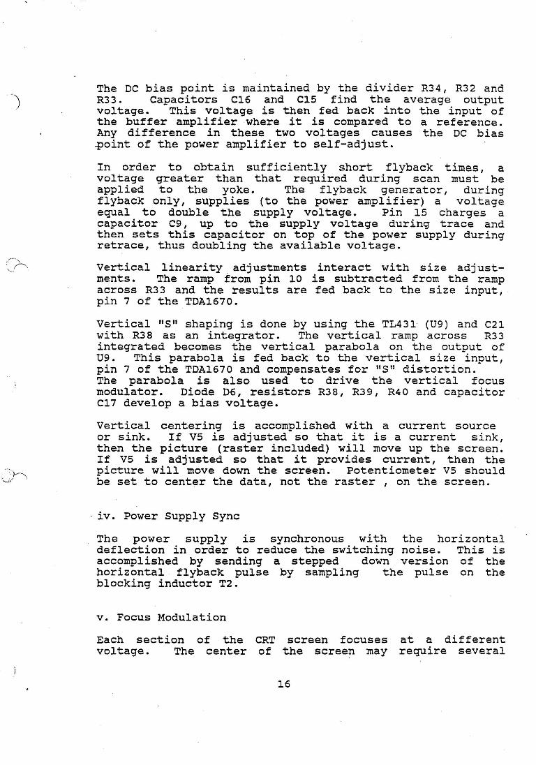
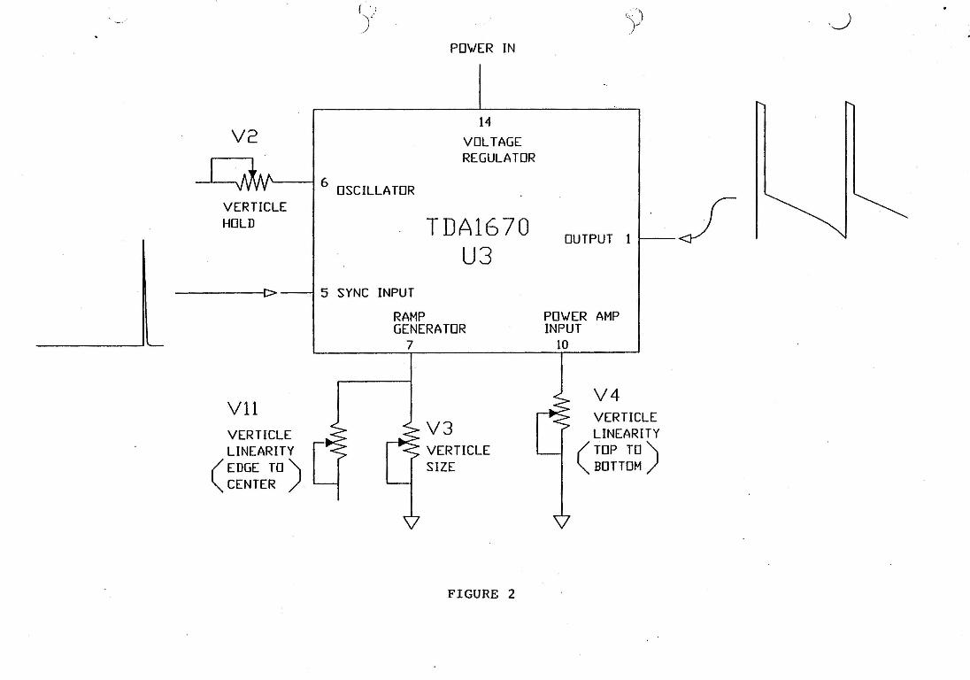
The TDA1670 incorporates all the necessary functions for providing the yoke with the current required for vertical deflection. Incorporated in silicon is a synchronizable oscillator, ramp generator, voltage regulator, voltage doubler and power amplifier.
The oscillator is an integrator · (pins 4 to 3) and a two threshold comparator which switches pin 6 high or low to allow the charging of CS. 03 allows the charge and discharge ramps to have adjustable slopes. Vertical sync pulses come in on pin 5. See figure 2.
The ramp generator is made up of a current generator, controlled by current through pin 7, and the capacitor C12 from pin 9 to ground. The slope and thus the size of the linear ramp is adjustable by setting the current pulled from pin 7 through V3. This ramp also appears buffered on pin 10 at a much lower impedance.
The power amplifier, with input on pin 12, sums the ramp on pin 10 with the current ramp through the yoke. R31 and C14 stabilize the high gain power amplifier. Yoke current flows from pin 1, through the yoke, the DC blocking capacitor Cl6, and the current sampling resistor R33 to ground. Voltage which represents yoke current is then fed back to the input of the amplifier to be compared with the reference.
The output stage of the power amplifier is supplied by the 25 volt supply during the trace, and by the flyback generator circuit during the retrace. The internal clock turris off the lower output stage to start flyback. The power output stage is thermally protected by sensing the junction temperature and shutting off the current source of the power stage.
15
The DC bias point is maintained by the divider R34, R32 and R33. Capacitors C16 and C15 find the average output voltage. This voltage is then fed back into the input of the buffer amplifier where it is compared to a reference. Any difference in these two voltages causes the DC bias ~oint of the power amplifier to self-adjust.
In order to obtain sufficiently short flyback times, a voltage greater than that required during scan must be applied to the yoke. The flyback generator, during flyback only, supplies (to the power amplifier) a voltage equal to double the supply voltage. Pin 15 charges a capacitor C9, up to the supply voltage during trace and then sets this capacitor on top of the power supply during retrace, thus doubling the available voltage.
Vertical linearity . adjustments interact with size adjustments. The ramp from pin 10 is subtracted from the ramp across R33 and the results are fed back to the size input, pin 7 of the TDA1670.
Vertical "S" shaping is done by using the TL431 (U9) and C21 with R3 8 as an integrator. The vertical ramp across R3 3 integrated becomes the vertical parabola on the output of U9. This parabola is fed back to the vertical size input, pin 7 of the TDA1670 and compensates for "S" distortion. The parabola is also used to drive the vertical focus modulator. Diode 06, resistors R38, R39, R40 and capacitor C17 develop a bias voltage.
Vertical centering is accomplished with a current source or sink. If V5 is adjusted so that it is a current sink, then the picture (raster included) will move up the screen. If VS is adjusted so that it provides current, then the picture will move down the screen. Potentiometer vs should be set to center the data, not the raster , on the screen.
· iv. Power Supply Sync
The power supply is synchronous with the horizontal deflection in order to reduce the switching noise. This is accomplished by sending a stepped down version of the horizontal flyback pulse by sampling the pulse on the blocking inductor T2.
v. Focus Modulation
Each section of the CRT screen focuses voltage. The center of the screen may
16
at a different require several
,-) hundred volts less than the top or bottom of the screen, while the left and right require more.
To achieve the best focus over all, the focus voltage is modulated with both a vertical and horizontal signals. The vertical parabola developed at U9 drives the emitter of the common base configured Q5 which is a high voltage amplifier. The collector of Q5 then has a high voltage parabola of vertical frequency.
The horizontal focus parabola is developed from the voltage on "S" capacitor C25. The parabola developed from the yoke deflection current at C25 is stepped up through T3 and added to the vertical parabola at Q5 to provide the focus voltage.
The autotransformer T3, is a multitapped transformer to accommodate different "S" capacitor waveforms and CRTs. The focus potentiometer V6, sets the DC focus voltage.
vi. High Voltage Shut Down/Spotburn Protection
If the deflection circuitry, horizontal or vertical, stops functioning at required frequencies, the high voltage supply will be shut down. If Q9 does not receive· a signal at the horizontal rate, C39 will charge up and turn Q10 on which will provide a positive voltage to the remote shut down pin on the power supply causing the high voltage to shut down. Likewise, if QS does not receive a signal at the vertical rate C38 will charge up and turn on Q10 resulting in high voltage shut down.
11.2 Power supply
11.2.1 Low Voltage Supply
The design utilizes a discontinuous flyback topology operating in current-mode resulting in a multiple output switcher with outputs which track well. Small or no output filter chokes are needed and slower diodes can be used. The fast transient response of the control loop maintains picture integrity. Very fast current limiting protects the switcher against short circuit.
The input rectifier section converts the AC line voltage into a crudely filtered and unregulated DC voltage, which powers the switching regulator. The input section is configured as a fullwave bridge when operated from 220V line, and as a voltage doubler when operating from 110V~ There is a header available to select either mode of operation.
17

:.:>. '' ... (~
/
To reduce noise low pass filter is reduced by transformer.
transmission to and from the power line, a isolates the switcher. The conducted noise X and Y capacitors and a common mode
3842 (Ul) , is an integrated current mode pulse width modulator. It consists of an oscillator, error amplifier, current sense comparator, under~voltage lockout and an output MOSFET driver stage. The under-voltage lockout circuit insures that Vee is adequate to make the 3842 fully operational before enabling the oscillator, voltage reference or output stage. Turn-on turn-off are fixed internally at 16V and lOV respectively. The 6V hysteresis prevents Vee oscillations·during power se~uencing.
The oscillator consists of a pull up resistor Rll, from the SV reference to pin 4 and a timing capacitor to ground. When the voltage ramps up to 2.8V on pin 4, an internal current sink pulls down, discharging the timing capacitor to a l.OV level. This level releases the current sink and starts the next cycle. The free running oscillator frequency is approximately equal to 1/.SSRC.
3842 can also be synchronized to an external clock. This is achieved by capacitively coupling a stepped down signal of the horizontal flyback pulse through C33 to the timing capacitor ClO. Noise immunity is enhanced if the free running frequency of the oscillator is set to be about 20% less than the clock frequency.
The output stage of the 3842 has a single totem-pole output capable of operating to lA peaks and a 200 mA average current.
3842 utilizes a current sense comparator. current mode controllers inherently keep close watch over the pass transistor 1 s current Ql. Pin 3 is connected to a voltage comparator which shuts off the output when the current in the primary winding of the power transformer reaches the desired level, as prescribed by the error amplifier. This way the controller will only allow the needed amount of power to be stored in the output transformer.
current mode control differs from most pulse width controllers which compare the error amplifier's output against the oscillator 1 s voltage ramp. This results in control of on-time, which does not necessarily mirror the power stored in the transformer.
18

-, ·'
The current sense comparator also serves the dual purpose of monitoring current limit. If pin 3 rises above lV the · output is terminated. Therefore, output short-circuits and core saturations should be detected before destroying Ql.
The error amplifier of the 3842 has the inverting input on pin 2, non-inverting input tied to an internal 2. 5 v reference and an output on pin 1. The voltage on pin 2 is compared to the 2.5V. Errors in output voltage are amplified and fed to pin 1 where they are frequency compensated by an RC back to pin 2. This error voltage is internally dropped by 1. 4V and divided by 3 before being fed to the current comparator. At the current comparator, the error amplifier output sets the level at which the current sensed at pin 3 will ramp up to, thereby setting the amount of energy stored in the power transformer and therefore, the power at the output.
In this application, an operational amplifier U4, located on the secondary side of the switcher, .compares a single output voltage to a regulated reference voltage. Any error in output voltage is amplified by U4. The output is frequency compensated by R24 and C24. Error current is fed through the optocoupler to the error amplifier of the 3842.
3842 draws v.ery little current in start-up mode. There is enough power from the line bleeders R2 and R3 to slowly charge C8 to the· 16V needed to start the switcher. When switching begins, Vee falls quickly but before it reaches the lOV shut-off level the auxiliary winding on the power transformer provides the required power.
As the 3842 starts a cycle, it turns on transistor Ql. This allows current to flow in the primary of Tl. As current ramps up with time, the voltage .across the current sense resistor R7 also ramps to a point where Ul determines enough power has been stored via the comparator, and turns off Ql. As the voltage on Ql flies upward, power is dumped from the main power transformer T1 through diodes into the different outputs. Primary ringing which could over voltage Q1, is clamped by D2. Currents from the secondary windings are rectified and filtered to create the desired output voltages.
11.2.2 High Voltage Supply
The high voltage power supply is a resonant mode regulator. The input supply voltage is 25V DC. The 25V input is regulated down to 15V by U3. This regulated lSV is divided down and used as the reference voltage input of the operational amplifier U4. The inverting input is the
19

feedback from the anode. POT2 adjusts the reference voltage for the non-inverting input and thus the anode voltage. In addition to the anode voltage, 1200V and -120V are developed from the same transformer.
The remote shutdown will shut the high voltage supply down if the voltage at the base of QS reaches approximately 6V.
20

("'-......
f·.:~~-
11.4 Analog Video, Low Bandwidth
The low bandwidth analog video board has a bandwidth of about 90MHz. It uses the MC10115, (U201 and U202) quad differential amplifier. The general circuit consists of a sync stripper, sync separator, de restore and video amplifier. The analog board also provides arc protection similar to the 1BIT ECL video board.
The sync stripper consists of Q202, Q203 and their supporting circuitry. This circuits' function is to remove the sync signals and to provide a composite sync signal for further processing.
Some setups require a separate composite sync signal from the video signal. These systems would not require a sync stripper and only need proper termination supplied by R237 and R236. Note that R236 arid R237 are optional components, however in case of R236 optional applies to it's value. If composite video is used R236 should be a lk ohm resistor.
The sync separator separates the vertical sync signal from the composite signal. This is accomplished with an exclusive OR gate, U204A. One input is tied directly to the composite sync and the other to a filtered composite sync. The horizontal rate is filtered out by R234 and C223. The output is a negative vertical sync signal. Composite sync is used for the horizontal sync signal.
The de restore circuit tells the video amplifier what voltage level represents a black video level. The video voltage level is sampled during blanking and compared to a reference voltage (set by R238) by U203B. The trailing edge of the horizontal sync is used to shut Q2 04 off. This turns on Q205 and allows a sample of the cathode voltage to reach the operational amplifier U203B. The output of U203B is fed to U202 and U201.
The video amplifier circuit consists of U201, U202, Q207, Q208 and Q209 and their supporting circuitry. U201 and U202 compare the black level set by U203B to the input video signal and amplify the difference. R211 sets . the input level and therefore the gain. The outputs of U201 and U202 together act as another differential amplifier, increasing the gain of the circuit. The remote contrast pot sets the current draw through Q2 07, which sets · the swing on the cathode.
Pin 1 of the MC10115 is the collector of . the output transistor and pin 2 · (3, 14, 15) is the emitter. Tying the emitters together gives the differential amplifier
22

~ ··~ ·~
configuration of 0201 and 0202. The inverting inputs of 0201 are tied to the non-inverting inputs o·f 0202 and visa versa. The larger the difference between black and input video levels, the more 0201 turns on (the less 0202 turns on) , which in turn drives Q207 on, forcing the cathode lower, resulting in a brighter video.
C203, C204 and C205 are peaking capacitors. R211 sets gain or contrast as does the remote contrast potentiometer.
11.5 Analog Video, Medium Bandwidth
The medium bandwidth analog board has a bandwidth of about 135MHz. It's functions are sync signal stripping, sync signal separation, DC restore and video amplification. It also provides arc protection for all circuitry.
The sync stripper consists of .U105A, Q103, Q104 and Q105 and their supporting circuitry. The collector of Q105 has the composite sync signal stripped from composite video. Some setups have a separate sync signal from video signal. This is allowed by JR101. Composite video uses JR101-A and separate sync uses JR101-B.
The sync separator separates the vertical sync signal from the composite signal. This is accomplished with an exclusive OR gate, U10~D. One input is tied directly to the +5V line and the other to a filtered composite sync. The horizontal rate is filtered out by R132 and C118. The output is a negative vertical sync signal. Composite sync is used for the horizontal sync signal.
The trailing edge of the horizontal sync activates Q106 causing a positive gate signal to pin 5 of 0101 for 0101 to sample the black level video. 0101 is a video preamplifier with internal black level restore and gain control. The output is coupled to Q101 where it is buffered and sent to the video driver amplifier 0102.
Ul02 is an LH2424 video driver amplifier. It operates off a 60V supply. The input on pin 1 is amplified and drives the output, pin 9, which is coupled to the cathode.
R106 controls the DC level or black level. R108 limits the range of the remote contrast potentiometer. JR101 is used to select between separate and composite sync. JR102 is set, so pin 6 on U103 has a negative going sync output. Cl11 and C112 are peaking capacitors.
23

APPENDIX
---""' : /-.,\

(
) '
f C> -
TIME·
6
Vee
, -) t •'
OUTPUT~ <lf---
5 'ERRDR V
DUTY C
MC1391 U2
RAMP IN~<l---
GND 2
FIGURE 1
·J
----'
Vll VERTICLE LINEARITY
(EDGE TO) CENTER
( . '
_f PD'JER IN
V3 VERTICLE SIZE
FIGURE 2
·· ') y ·
V4 VERTICLE LINEARITY
(TOP TO) BOTTOM
·J

( .•
) r ' ) _y \_)
DEFLECTION BOARD
I~OW'ER SUPPLY FOCUS (YJ
"' ... MODULATION
~ ..
Gl AND G2 I .. CONTROLS ..
- LO\.J VOLT AGE ~ .. ~ VIDEO BOARD ~~ f-- t t ~
-+ ~ f'(N[R I ~ I I CRT i ... ~ I ..
SOCKET l YOKE _I ~ ~ f'DII(R"" VERTICLE HORIZONTAL i DEFLECTION _j t_ DEFLECTION .. ~ 4 VIDEO
J .. CIRCUIT CIRCUIT .. AMPLIFIER HIGH VOLT AGE .. ~ r
~ .
' ' I I · r.:: I'IJII£R SYNC _,--..,. ~~ ...
PROCESSING ....
+ SYNC INPUT Jl
, '"''' T"\1 llf'l/ T'ITArnAt-..1

(
( ) ~ .. _ .... ./
MONITOR DOES NOT TURN ON LED DOES NOT LIGHT
LOOK TD DEFLECTION BOARD
IT HAY BE NECESSARY TO USE EXTERNAL PDVER SUPPLY TD DETERMINE DEFLECTION BOARD STATUS
i' ·\ ))
APPLY POVER
REMOVE POVER SUPPLY f'ROH UNIT
HEASURE OLD6,07,DB.D9,DIO,Dl2 Q3,DI3,DI4 VITH OHH HETER
\J

...___,.
~HDb~041\ o.0022ur~
1 ekl~----. Rl7 J90K
Rl6 270K
·_)
JS
F2 J ~-tJ. .. _rETour O.lur I CJ
C~r:-:: Dl cs n1 ~ C4 ±
:r..::...:..- -~ ..__~--;;0~0047ur --. RS40SL DRIUGE C6
O.OOHuF~· C39 "; .¢.
Cl6 r/7 ~:r~r
2 Ul
R2 47K
UCJ0-12 61 R9'W-M I
a r
5 3
)l
In~ 95V/I20V
Tl
C22
i} 330vF
---o+OSV I ()l
IN-1937 JJOvr JOOV C21
"
"v LJ ~J---o•-IOV
Cll I O.luF .}.. 022 I I J_ Cl2 ..L CIO I L T'""" T '"' r{';.;oue ~ik~ ~ .~~- l.~l} T ~,',';, I I t-.-.+----l-----l. _ _L_jt---J
~IOTE• 06 <IN~H6 ZENER> NOT INSTI\LLEO DET~EEN GI\TE 1\ND SOURSE OF 01
J4
( C1dJdJ ~ ~ ~ =u= ~ !}={]] HIGH VOLT AGE
HIIT(RII\Lo scl\lt• NONE I s~rcr' 1 or 2 1------------------1 -lll\l(o OJ-09-09 R[VI$1()11 A
mLt:• P65-02 PO\./ER SUPPLY rlfiiSII•
I I PRI\IJII DY• DRIIIIIUG I
MINH TRAN CIICCKtO RYo
4100 souru vcsr TEHPLt: VSCS-02A I Dlrtr.IIIIIJ'I ••c '" IH!:Ir:r "''~ ntGRI:B Sllll li\K[ CIIY, UTIIII 011D71Jtf\.(SS OIII[RIIIS[ SPt:CirlrJ'l· llURMO([I ~t ... !" .Ol .nt:!: 003. •ooCUI '!I DtG.
FN : q co- OQC.)~:> - c:::;1C)
.· .. :.. .... , ___ .. : .. _, .. ____ _
l'i .I . !· · ( , I t:!
~ - ~
r~ . ~.
f .. , li ' : ·. ' .· F -!
;.
l
k ~ :·. ·' I ;, '
!~ I
! ~
I f: .. f' I· i ' ,. ,. ;, ;,

~ I
'-. ... /
fRDH SHEET I (+27V> L4 200vH
C26
0 220ur J
p1n5 _J_ R35 IOK
C25 o.Jur
R25 100
()'
D20. fDH333
R22
~~ I -::- R23 ~.7K "#Nv IK -
~ '" ""TPor,-cz4 J9pr 75K ~
0 1 FRDH SHEET I (+85V>
plnB
REMOTE SIIUTDOVN
CJI o.o47ur
.... ... '
R32 10
---=t_
~-CJO _lOOluF
HATERII\L•
))
'·
,,,.
HIGH VOLTAGE SECTION
+ 1200V
-I20V
-o
0 pln3
~-----------------------~ plnl
( (]d]dJ ~ §) ~-~ ~ []={]] HIGH VOLT AGE
TlrLI:• P65-02 PO'WER SUPPLY
II[ VIS lOll
sci\Lt• NONE 1 sun' 2 or 2
I rJNISJio I IJAI[o OJ-09 - 09 (\
l·-;;ll;RI\;;V:I;::N;G-~:;-------------IIlRI\VII IJ'I'o MINH TRAN CII£CK[O bY•
I 4100 soum VEST TtHf'L[ I VSCII 02A I D111·11m••l ••r '" rrtf•n .,,n ncr,orn SIIU LIIK( CIIY, Ufllll 04107 -- · ur.n..CSS lllli[RV~~E SI'[CirltP. llk i.RNIClS MC .U!OL .•u,!.OO,, Ntrolt . .:..S.::.!..:..I..:.OC..:..e>:_ ______ , ____ ...J
-n" ,. r• . ,...
!,' ... ~
r. I, . r.· . I'
li ·~ .. •;I ·,;
! '
~,_,,.,: ;:
; . v·. i.'. ~ · r· .·.· "· ,.
i.
r I . I
\, 'i I
~ .
t ! '• I ! p I';
t:. 'I ,, ., ,. , .. F i,:
r ·,.
t

montTERm CORPORaTIOn Configuration and Alignment Specification
Customer Viking VCX 91 DPI 220V
Procedure High Pot Test Bum-In Visual Inspection Preliminary Setup Monitor Serup Display Orientation High Voltage Page Size Page Centering In Raster Video Centering Vertical Linearity Horizontal Linearity
. --~ Pincushioning Vertical Hold Remote Brightness lli ghline/Low line Intermi ttenc:e Phase Locked Loop Drift Switching Power Supply Brightness Display Quality Focus Horizontal Retrace Spot Kill AC Power Cycling 120 Volt Operation Adhesives Wrap-Up Auxiliary Power Check
Para~raph 38.2 37.1
4.1 5.2 5.4
34.1 6.1 7.4 8.6 8.7 9.5
10.5 18.4 23.3 11.2 12.1 17.1 13:3 20.6 14.5 16.1 15.6 27.1 19.1 36.1 26.10 24.0 32.1 47.1
Part Number 903-0279-03 Rev. B
Parameter Limits Maximum Leakage Current 11mA Use 1/2 Amp 9 Volt DC Load Phillips 72J.!H, SPS Tap 2-5 ECL video, Viking Cable with LED Lowline = 198 VAC; Nominal = 220 V AC LMLS•UL 18,000 VDC; ±100 VDC 82.0V ±l.OV, 14.0" X 10.50" ±0.10" Dead Center Mechanical Center 5% Maximum 10% Maximum Screen Facing Magnetic North
Leave Remote For Max. Intensity 265/198 V AC 60Hz
0.10" Maximum Tap 2-5 G2= 650 VDC, ±30 FootlambertS ±3fL Use Reference Display Reference Q1002, Paragraph 9 Height 615V; Time 2.6 ±0.1J.1.Sec (REF)
5 Cycles Minimum 90/135 V AC 60 Hz
Are you proud of this monitor? -9 VDC on pin 5 of 9D
Special Instructions
Final alignment must be done on Moniterm 91 DPI controller card.
Quantum Generator Settings Timing: Horizontal: Vertical: Dot Rate 62.176MHz Dots/Character 9 Lines/Character Horizontal Rate 66.43 KHz Total 104 Total Vertical Rate 66.43 Hz Characters 80 Rows
Drive Delay 78 Drive Delay Step 2 Drive Width 4 Drive Width
16 1000 60 60 3
All OP Codes Arc Zero Except: OP3.1, OP7.1, OP 12.2, OP 14.1, OP 16.3
Set Moniterm video
generator outputs to:
. : .. ::_ ·.~·;·"'· :··
OP4.1, OP 8.1,
Video: +,Reverse
H./C. Sync: H. sync
OP 13.3,
Bit 3: Off
H Sync:-
OP 15.2,
Bit2: Off
V sync:-
Bit 1: On