Electronic Part Failure Analysis Tools and Techniques · Web viewFurthermore, parts removed for...
20
Electronic Part Failure Analysis Tools and Techniques Walter Willing Jonathan Fleisher Michael Cascio Walter Willing Jonathan Fleisher Michael Cascio Northrop Grumman Corporation Willing, et al: page 1
Transcript of Electronic Part Failure Analysis Tools and Techniques · Web viewFurthermore, parts removed for...
Electronic Part Failure Analysis Tools and Techniques
Walter Willing
Jonathan Fleisher
Michael Cascio
Walter WillingJonathan FleisherMichael Cascio
Northrop Grumman Corporation7323 Aviation Blvd,
Baltimore, MD, 21090, USAe-mail: [email protected]
[email protected] [email protected]
Willing, et al: page 1
SUMMARY AND PURPOSEThe current emphasis on Physics of Failure (PoF) and accurate Root Cause Analysis (RCA) highlights the need for effective electronic part failure analysis processes and capabilities. Failure analysis can be as simple as visually inspecting a part and as extensive as performing sub-micron level cross-sectioning of silicon die using Focus Ion Beam (FIB) technology. This tutorial presents a “Process” as well as the tools and techniques required to perform effective failure analyses on electronic components. In addition, the common failure mechanisms found in electronic hardware are explained and emphasized with a case study.
Walter WillingMr. Willing is a Senior Advisory Reliability Engineer within the Northrop Grumman Corporation Electronic Systems Sector, System Supportability Engineering Department. Mr. Willing has over 30 years experience in space systems reliability. He received a BSEE from the University of Delaware and an MSEE from the Loyola College of Maryland. He is active in the IEEE (Sr. Member, Vice Chairman of the Baltimore Section), IEST and serves on the RAMS Management Committee. He has authored five peer reviewed technical papers and one RADC publication.
Jonathan Fleisher Mr. Fleisher is a Principal Reliability Engineer within the Northrop Grumman Corporation Electronic Systems Sector, System Supportability Engineering Department. Mr. Fleisher received a BSME and an MSIE from New Mexico State University. He has 16 years of engineering experience on a variety of defense related programs, with multiple Systems Engineering responsibilities, including Environmental Qualification Lead on several radar programs. During the last several years, he has focused on reliability engineering for NGC Space Programs.
Michael CascioMr. Cascio is a Failure Analysis and Reliability Engineer within the Product Integrity Department of the Northrop Grumman Electronics Systems Sector in Baltimore Maryland. Mr. Cascio received a BSEE from The Pennsylvania State University. He has over 20 years of electronic experience in Radar, Reliability and Failure Analysis. He spent eleven years in the United States Air Force where he managed operations, maintenance and support equipment for 20 two million dollar radars. He also directed the research and development upgrades on the enhancement of radar systems. At Northrop Grumman he has 10 years of engineering experience in Failure Analysis and Reliability.
Table of contents
1. Introduction ...............................................................................................................................................12. Importance of Effective Failure Analysis..................................................................................................13. Basic Failure Analysis Techniques............................................................................................................24. Suggestions For Your Own Failure Analysis Capabilities........................................................................75. Understanding Electronic Part Failure Mechanisms..................................................................................76. Failure Analysis Case Study......................................................................................................................117. Conclusions................................................................................................................................................128. References..................................................................................................................................................12
Willing, et al: page 2
1. INTRODUCTION
Organizations that produce electronic hardware should have some level of electronic part failure analysis capability and knowledge of where to go for extended failure analysis. The failure analysis process is also important. First, it is important to verify and characterize the failure via electrical test. Subsequent steps should involve non-invasive examinations such as microscopic visual inspection, X-ray and hermetic seal tests. Finally, after all non-invasive tests are completed, devices can be de-lidded (or de-capsulated) and silicon die inspections and evaluations can be performed. This tutorial discusses the fundamental electronic part failure analysis processes, methods, tools and techniques that can be utilized to accurately determine why devices fail. This tutorial is an expansion of the 1997 O.A. Plait award winning tutorial “Understanding Electronic Part Failure Mechanisms”, sections of which are repeated in this tutorial (refer to Section 5). It is important to know what the common part failure modes are as well as the failure analysis techniques used to find them. Understanding the cause of the part failure allows for effective corrective action and the prevention of future occurrences. Suggestions for several levels of failure analyses capabilities will be presented (Basic, Moderate, Advanced) as well as some examples of actual failure analyses to illustrate what actually occurs in failed hardware.
2. IMPORTANCE OF EFFECTIVE FAILURE ANALYSIS
When electronic parts fail, it’s important to understand why they failed. Effective root cause analysis of part failures is required to assure proper corrective action can be implemented to prevent reoccurrence. Determination of root cause is also important for High Reliability systems such as implantable medical devices, space satellite systems, deep well drilling systems, etc, where failures are critical, as well as consumer products where the cost of a single failure mode can be replicated multiple times. A common term for the process of root cause determination and applying corrective action is called FRACAS (Failure Reporting, Analysis and Corrective Action System). Failure Analysis is the crucial part of the FRACAS process. Failure Analysis must be performed correctly to assure the failure mechanism is preserved, not “Lost” due to carelessness, bypassing critical measurements or performing destructive analyses in an incorrect sequence. For example, once wirebonds are removed, the part may not be able to be electrically tested. Furthermore, parts removed for failure analysis may “Re-Test OK” (RTOK) as a result of the wrong part being removed, or the fact that testing does not properly capture the part’s failure mode (such as a subtle parameter shift) or a particular failure sensitivity (gain vs temperature) exists. Since it is important to preserve and characterize the failure mode to the greatest extent possible, this tutorial presents a suggested failure analysis flow, starting with full part failure characterization, followed by non-invasive and finally invasive failure analysis techniques.
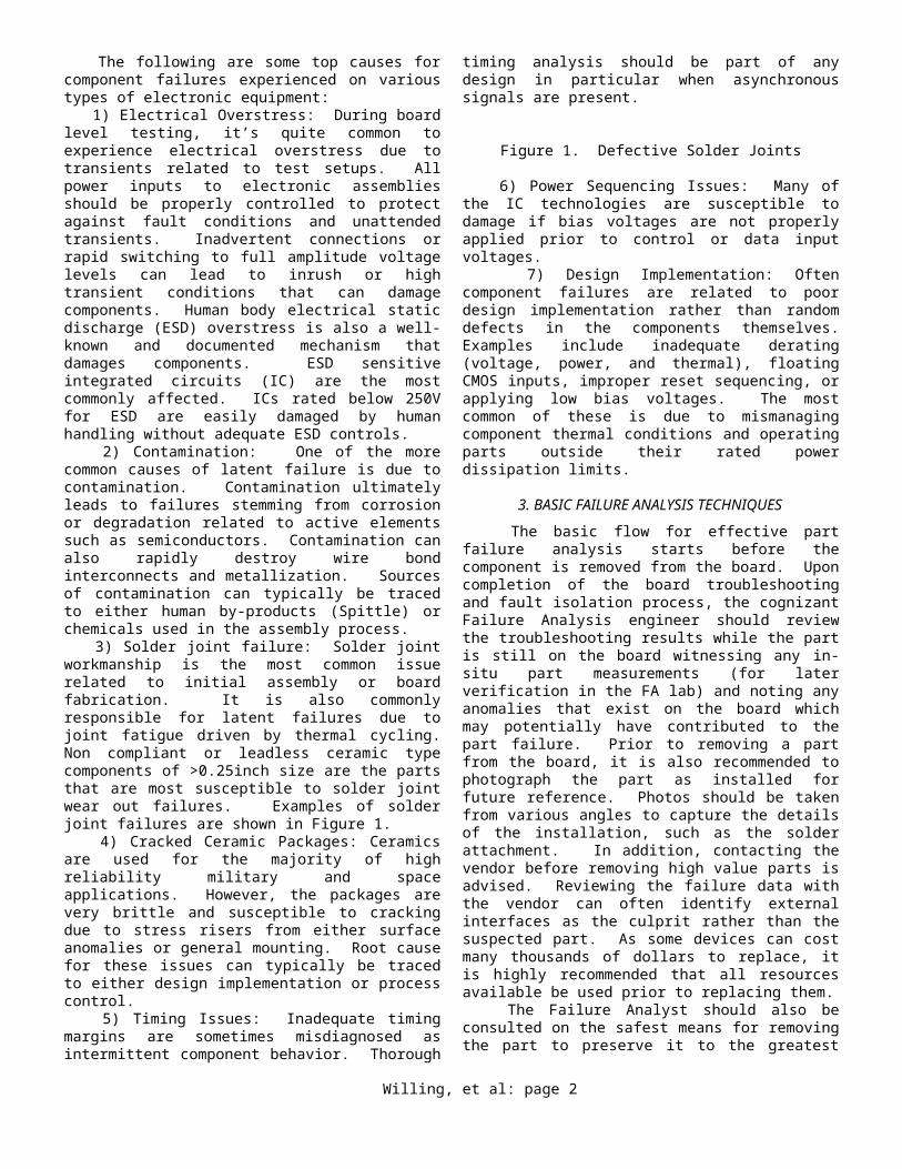
The following sections herein address basic failure analysis techniques. Additional information on failure analysis methods can be found in Mil-Std-883 and Mil-Std-1580. While these specifications define test and evaluation methods, the “requirements” and methods within these standards provide a good baseline for evaluating failed parts. For example, when evaluating the wirebonds on a failed part, the pull test limits in Mil-Std-883 (Method 2011) can provide insight as to whether the failure part has good wirebonds. The internal visual inspection criteria of Mil-Std-883 (Methods 2010 and 2017) help determine whether any anomalies are actually defects or allowed process variations. For further investigation into advanced failure analysis techniques and component failure modes, the reader is encouraged to become familiar with the International Reliability Physics Symposium (IRPS) as well as other venues. The following are some top causes for component failures experienced on various types of electronic equipment: 1) Electrical Overstress: During board level testing, it’s quite common to experience electrical overstress due to transients related to test setups. All power inputs to electronic assemblies should be properly controlled to protect against fault conditions and unattended transients. Inadvertent connections or rapid switching to full amplitude voltage levels can lead to inrush or high transient conditions that can damage components. Human body electrical static discharge (ESD) overstress is also a well-known and documented mechanism that damages components. ESD sensitive integrated circuits (IC) are the most commonly affected. ICs rated below 250V for ESD are easily damaged by human handling without adequate ESD controls. 2) Contamination: One of the more common causes of latent failure is due to contamination. Contamination ultimately leads to failures stemming from corrosion or degradation related to active elements such as semiconductors. Contamination can also rapidly destroy wire bond interconnects and metallization. Sources of contamination can typically be traced to either human by-products (Spittle) or chemicals used in the assembly process. 3) Solder joint failure: Solder joint workmanship is the most common issue related to initial assembly or board fabrication. It is also commonly responsible for latent failures due to joint fatigue driven by thermal cycling. Non compliant or leadless ceramic type components of >0.25inch size are the parts that are most susceptible to solder joint wear out failures. Examples of solder joint failures are shown in Figure 1. 4) Cracked Ceramic Packages: Ceramics are used for the majority of high reliability military and space applications. However, the packages are very brittle and susceptible to cracking due to stress risers from either surface anomalies or general mounting. Root cause for these issues can typically be traced to either design implementation or process control. 5) Timing Issues: Inadequate timing margins are sometimes misdiagnosed as intermittent component behavior. Thorough timing analysis should be part of any design in particular when asynchronous signals are present.
Willing, et al: page 1
Figure 1. Defective Solder Joints
6) Power Sequencing Issues: Many of the IC technologies are susceptible to damage if bias voltages are not properly applied prior to control or data input voltages. 7) Design Implementation: Often component failures are related to poor design implementation rather than random defects in the components themselves. Examples include inadequate derating (voltage, power, and thermal), floating CMOS inputs, improper reset sequencing, or applying low bias voltages. The most common of these is due to mismanaging component thermal conditions and operating parts outside their rated power dissipation limits.
3. BASIC FAILURE ANALYSIS TECHNIQUES
The basic flow for effective part failure analysis starts before the component is removed from the board. Upon completion of the board troubleshooting and fault isolation process, the cognizant Failure Analysis engineer should review the troubleshooting results while the part is still on the board witnessing any in-situ part measurements (for later verification in the FA lab) and noting any anomalies that exist on the board which may potentially have contributed to the part failure. Prior to removing a part from the board, it is also recommended to photograph the part as installed for future reference. Photos should be taken from various angles to capture the details of the installation, such as the solder attachment. In addition, contacting the vendor before removing high value parts is advised. Reviewing the failure data with the vendor can often identify external interfaces as the culprit rather than the suspected part. As some devices can cost many thousands of dollars to replace, it is highly recommended that all resources available be used prior to replacing them. The Failure Analyst should also be consulted on the safest means for removing the part to preserve it to the greatest extent possible. Once the part is removed for failure analysis, three (3) basic processes should be followed:
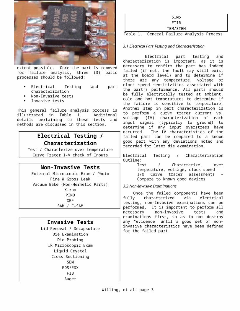
Electrical Testing and part characterization Non-Invasive tests Invasive tests
This general failure analysis process is illustrated in Table 1. Additional details pertaining to these tests and methods are discussed in this section.
Electrical Testing / CharacterizationTest / Characterize over temperature
Curve Tracer I-V check of Inputs
Non-Invasive TestsExternal Microscopic Exam / Photo
Fine & Gross LeakVacuum Bake (Non-Hermetic Parts)
X-rayPINDXRF
SAM / C-SAM
Invasive TestsLid Removal / Decapsulate
Die ExaminationDie Probing
IR Microscopic ExamLiquid Crystal
Cross-SectioningSEM
EDS/EDXFIB
AugerSIMSFTIR
TEM/STEMTable 1. General Failure Analysis Process
3.1 Electrical Part Testing and Characterization
Electrical part testing and characterization is important, as it is necessary to confirm the part has indeed failed (if not, the fault may still exist at the board level) and to determine if there
Willing, et al: page 2
are any temperature, voltage or clock speed sensitivities associated with the part’s performance. All parts should be fully electrically tested at ambient, cold and hot temperatures to determine if the failure is sensitive to temperature. Another step in part characterization is to perform a curve tracer current vs. voltage (IV) characterization of each input signal (typically to ground) to determine if any input overstress have occurred. The IV characteristics of the failed part can be compared to a known good part with any deviations noted and recorded for later die examination.
Electrical Testing / Characterization Outline:Test / Characterize, over temperature, voltage, clock speedI/O Curve tracer assessments – Compare to known good devices
3.2 Non-Invasive Examinations
Once the failed components have been fully characterized via electrical testing, non-Invasive examinations can be performed. It is important to perform all necessary non-invasive tests and examinations first, so as to not destroy any “evidence” until a good set of non-invasive characteristics have been defined for the failed part.
3.2.1 External Microscopic exam / Photo
Using a stereo microscope, a thorough external visual examination of the suspect part should be performed early in the failure analysis process. Typical inspection scopes range from 10X to 30X magnification, which is usually sufficient to identify such items as external contamination and/or solder balls (possibly shorting out pins on the device), damaged leads or package seals, gross cracks in the package, etc. Magnification levels up to 100X can be employed to further examine any anomalies identified. The following conditions should be specifically looked for:
• Contamination• Mechanical damage• Thermal or electrical damage• Seal integrity• Lead integrity
Photographs should be taken to document the condition of the part and to record any anomalies.
3.2.2 Fine & Gross seal tests for hermetic devices
Hermeticity testing (refer to Mil-Std-883 Method 1014) should be performed on hermetic parts to ensure no leaks that could have allowed moisture to enter the package exist. Any internal moisture might result in possible corrosion or provide a conductive path on the semiconductor die surface, thereby causing a failure. A fine leak test often involves placing the part in pressurized helium (He) chamber in an attempt to force He into the device cavity through any leak sites, then moving the part to a Helium detection chamber to see if any He leaks out. Gross leak testing involves placing the part in a heated fluorocarbon bath and literally “Looking for Bubbles”. The heated bath causes the atmosphere within the package to
expand, forcing it through any large leak sites. It is important to perform both Fine Leak and Gross leak testing, as a Gross Leak site may be large enough to allow a full venting of the pressurized He, subsequently resulting in a false pass for the fine leak test. It is also important that the failed part be clean of any external epoxy or contamination that could absorb the He and provide a false positive reading. Newer optical leak test equipment using laser imaging of package lid deflection to confirm hermeticity is also available.
3.2.3 Vacuum Baking
If a non-hermetic part or cable is suspected to have a moisture related issue, a vacuum bake can be performed to drive out any residual moisture. If the problem disappears after the vacuum bake process, humidity could have been the cause. The authors were recently involved with a case where trapped moisture affected the performance of an RF cable.
3.2.4 X-ray (Film, Real-time, 3D)
Radiograph (refer to Mil-Std-883 Method 2012), often referred to as X-ray, is a very powerful tool for non-invasive failure analysis as X-ray can detect actual or potential defects within enclosed packages. There are multiple types of X-ray equipment available, from the basic film X-ray systems to real-time and 3-D X-ray systems. While film X-rays can be useful, the modern real-time X-ray provides a more extensive capability. Basic X-rays allow internal part examination looking for:
Internal particles Internal wire bond dress
i.e. can make sure the wire bonds are not touching each other or package lids
Die attach quality (voiding, die attach perimeter) Solder joint quality for connectors Insufficient or excessive solder Substrate or printed wiring board trace integrity Obvious voids in the lid seal Foreign metallic particles within the package Internal part orientation, etc.
The resolution of a basic film X-ray is typically to a 1 mil particle size, or bond wires to 1 mil diameter. The principal limitation of film X-ray is that it only allows one exposure level at a time. Not all characteristics can be observed at a single exposure level. Conversely, real-time X-ray typically has a resolution range from 1um to 0.4 um and allows for a continuous adjustment of exposure levels and conditions, as well as real time part rotation to obtain the most revealing X-ray view. Special digital filtering and image processing can also be used to detect possible delinations in the image not otherwise observable on the image screen.
3.2.5 PIND Test / Particle Impact Noise Detection (PIND)
Cavity device failures can be caused by internal conductive particles shorting adjacent conductors. While X-ray techniques can be used to detect internal particles, another method is Particle Impact Noise Detection (PIND), refer to Mil-Std-883 Method 2020. PIND Testing can be subjective and may not be
Willing, et al: page 3
easily performed on complex hybrids. However, it can provide evidence of internal particles. A common technique employed is to perform X-ray and PIND together; first an X-ray is taken, then the part is PIND tested, and then a second X-ray is taken. This allows one to identify particles that are free-floating within the package. Section 5.5.3 discusses loose particles detected during PIND test.
3.2.6 X-ray Fluorescence (XRF)
X-ray Fluorescence (XRF) is a non-destructive technique used to determine the elemental composition of solid and liquid samples. The X-rays excite atoms in the sample, causing them to emit X-rays with energies characteristic of each element present. The XRF equipment measures the energy and intensity of these X-rays and is capable of detecting elements from Al to U in the periodic table. XRF can determine concentrations ranging from parts per million to 100% at depths as great as 10µm. Using reference standards, XRF can accurately quantify the elemental composition of the samples. XRF is commonly used to examine platings for pure tin content, as well as for cadmium and zinc [1].
3.2.7 Acoustic tests (SAM / C-SAM)
Acoustic testing is a popular test method to look for voids and delaminations or cracks in Plastic Encapsulated Microcircuits (PEMS) and ceramic capacitors. Acoustic tests rely on acoustic energy transfer through the part. If there is a void, the acoustic energy is blocked and voids can be detected. The acoustic tests can also be tuned to attempt to determine the depth of any void. Acoustic tests involve either reflected acoustic energy or energy transmitted through the part. Since the energy transmission medium is typically deionized water, parts to be examined must withstand exposure to water.
3.2.8 Residual Gas Analysis, internal water vapor content
Before transitioning to invasive examinations, for a hermetic part suspected of having an internal moisture issue, then Residual Gas Analysis (RGA) should considered once all non-invasive tests are performed. If a part only fails at cold temperature, an RGA test should be considered as cold temperature failures may be a result of excessive internal moisture condensing on the die surface. RGA (refer to Mil-Std-883 Method 1018) involves “Poking a Hole” through the device lid, using a vacuum to remove the interior gas and performing a spectral analysis of the internal gases to determine their content. RGA can detect most of the gasses found within devices and report their individual concentrations. For water vapor, the maximum allowed concentration is typically 5000 ppm. This corresponds to the dew point (sublimation point) of -2C where the partial pressure of the H20 prevents any liquid condensation.
3.3 Invasive Examinations; Part De-Lid / De-Process
After all Non-Invasive examinations have been performed, it’s time to “Bite the Bullet” and dig deeper into the part. For
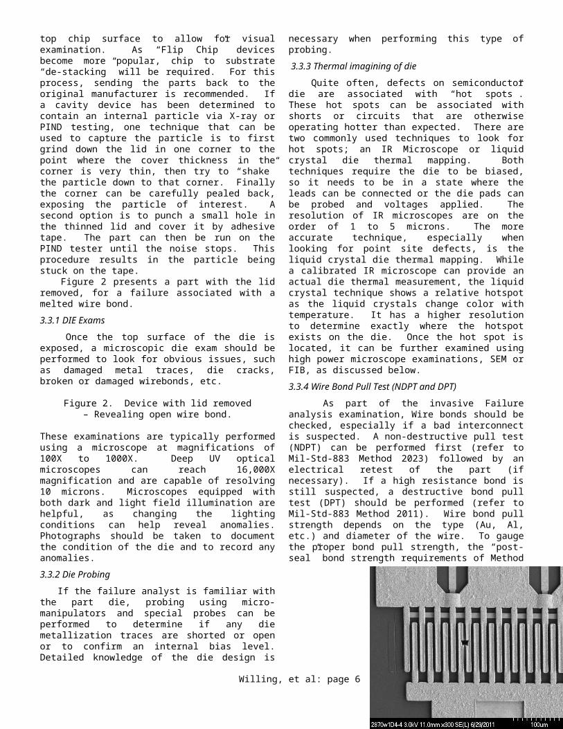
cavity parts, this often involves a process called “delidding” where the device lid is removed, often by grinding down the lid around the seal ring or weld seal. For Plastic Parts, a chemical vapor deprocessing (desolving) of the encapsulant material must be performed. In either case, the goal is to expose the top chip surface to allow for visual examination. As “Flip Chip” devices become more popular, chip to substrate “de-stacking” will be required. For this process, sending the parts back to the original manufacturer is recommended. If a cavity device has been determined to contain an internal particle via X-ray or PIND testing, one technique that can be used to capture the particle is to first grind down the lid in one corner to the point where the cover thickness in the corner is very thin, then try to “shake” the particle down to that corner. Finally the corner can be carefully pealed back, exposing the particle of interest. A second option is to punch a small hole in the thinned lid and cover it by adhesive tape. The part can then be run on the PIND tester until the noise stops. This procedure results in the particle being stuck on the tape. Figure 2 presents a part with the lid removed, for a failure associated with a melted wire bond.
3.3.1 DIE Exams
Once the top surface of the die is exposed, a microscopic die exam should be performed to look for obvious issues, such as damaged metal traces, die cracks, broken or damaged wirebonds, etc.
Figure 2. Device with lid removed – Revealing open wire bond.
These examinations are typically performed using a microscope at magnifications of 100X to 1000X. Deep UV optical microscopes can reach 16,000X magnification and are capable of resolving 10 microns. Microscopes equipped with both dark and light field illumination are helpful, as changing the lighting conditions can help reveal anomalies. Photographs should be taken to document the condition of the die and to record any anomalies.
Willing, et al: page 4
3.3.2 Die Probing
If the failure analyst is familiar with the part die, probing using micro-manipulators and special probes can be performed to determine if any die metallization traces are shorted or open or to confirm an internal bias level. Detailed knowledge of the die design is necessary when performing this type of probing.
3.3.3 Thermal imagining of die
Quite often, defects on semiconductor die are associated with “hot spots”. These hot spots can be associated with shorts or circuits that are otherwise operating hotter than expected. There are two commonly used techniques to look for hot spots; an IR Microscope or liquid crystal die thermal mapping. Both techniques require the die to be biased, so it needs to be in a state where the leads can be connected or the die pads can be probed and voltages applied. The resolution of IR microscopes are on the order of 1 to 5 microns. The more accurate technique, especially when looking for point site defects, is the liquid crystal die thermal mapping. While a calibrated IR microscope can provide an actual die thermal measurement, the liquid crystal technique shows a relative hotspot as the liquid crystals change color with temperature. It has a higher resolution to determine exactly where the hotspot exists on the die. Once the hot spot is located, it can be further examined using high power microscope examinations, SEM or FIB, as discussed below.
3.3.4 Wire Bond Pull Test (NDPT and DPT)
As part of the invasive Failure analysis examination, Wire bonds should be checked, especially if a bad interconnect is suspected. A non-destructive pull test (NDPT) can be performed first (refer to Mil-Std-883 Method 2023) followed by an electrical retest of the part (if necessary). If a high resistance bond is still suspected, a destructive bond pull test (DPT) should be performed (refer to Mil-Std-883 Method 2011). Wire bond pull strength depends on the type (Au, Al, etc.) and diameter of the wire. To gauge the proper bond pull strength, the “post-seal” bond strength requirements of Method 2011 should be considered (~ 80% of initial pull strength), to allow for some loss of bond strength with time and thermal exposure. For thermo-compression or thermo-sonic ball bonds, any bond pull failure where the entire ball bonds lifts off of the pad should be examined in more detail. These kinds of “ball lifts” are quite often a result of “Kirkendall voiding” and could represent a fundamental wire bond issue with the part. Section 5.1.1 discusses additional wire bond issues.
3.3.5 Cross Sectioning
Cross-Sectioning is a very important means of failure analysis. It is often used for connector, printed wiring board, substrate, solder joint, capacitor, resistor transformer, transistor and diode failure analysis. Cross-sectioning of semiconductor die can also be performed using a Focused Ion Beam (FIB). More information on FIB techniques is discussed in section 3.3.8. Prior to cross-sectioning, the sample is usually potted in a hard setting acrylic or polyester rosin. Cross-Sectioning is
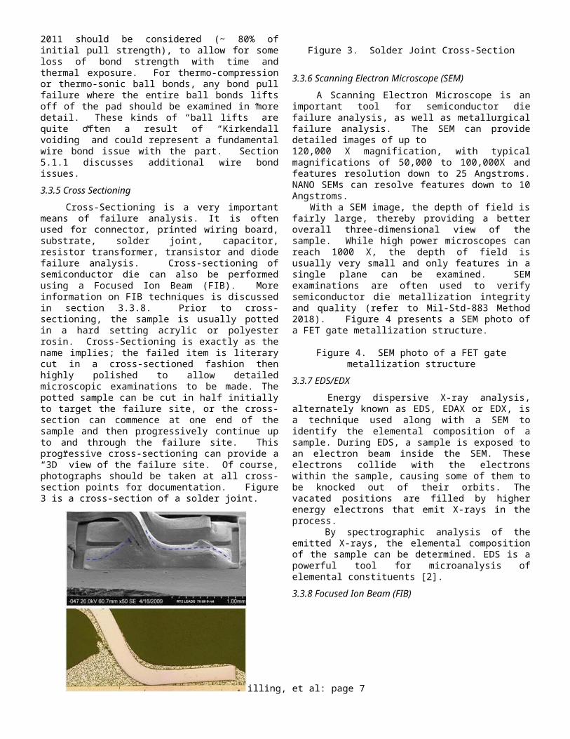
exactly as the name implies; the failed item is literary cut in a cross-sectioned fashion then highly polished to allow detailed microscopic examinations to be made. The potted sample can be cut in half initially to target the failure site, or the cross-section can commence at one end of the sample and then progressively continue up to and through the failure site. This progressive cross-sectioning can provide a “3D” view of the failure site. Of course, photographs should be taken at all cross-section points for documentation. Figure 3 is a cross-section of a solder joint.
Figure 3. Solder Joint Cross-Section
3.3.6 Scanning Electron Microscope (SEM)
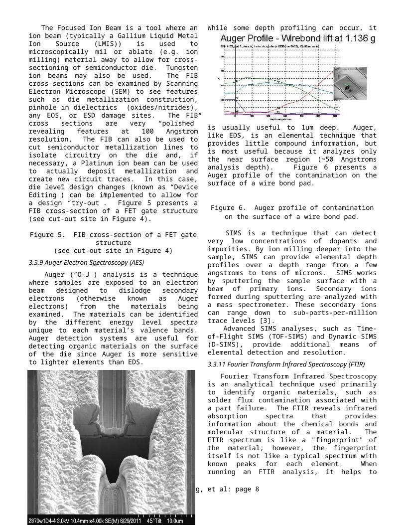
A Scanning Electron Microscope is an important tool for semiconductor die failure analysis, as well as metallurgical failure analysis. The SEM can provide detailed images of up to120,000 X magnification, with typical magnifications of 50,000 to 100,000X and features resolution down to 25 Angstroms. NANO SEMs can resolve features down to 10 Angstroms. With a SEM image, the depth of field is fairly large, thereby providing a better overall three-dimensional view of the sample. While high power microscopes can reach 1000 X, the depth of field is usually very small and only features in a single plane can be examined. SEM examinations are often used to verify semiconductor die metallization integrity and quality (refer to Mil-Std-883 Method 2018). Figure 4 presents a SEM photo of a FET gate metallization structure.
Willing, et al: page 5
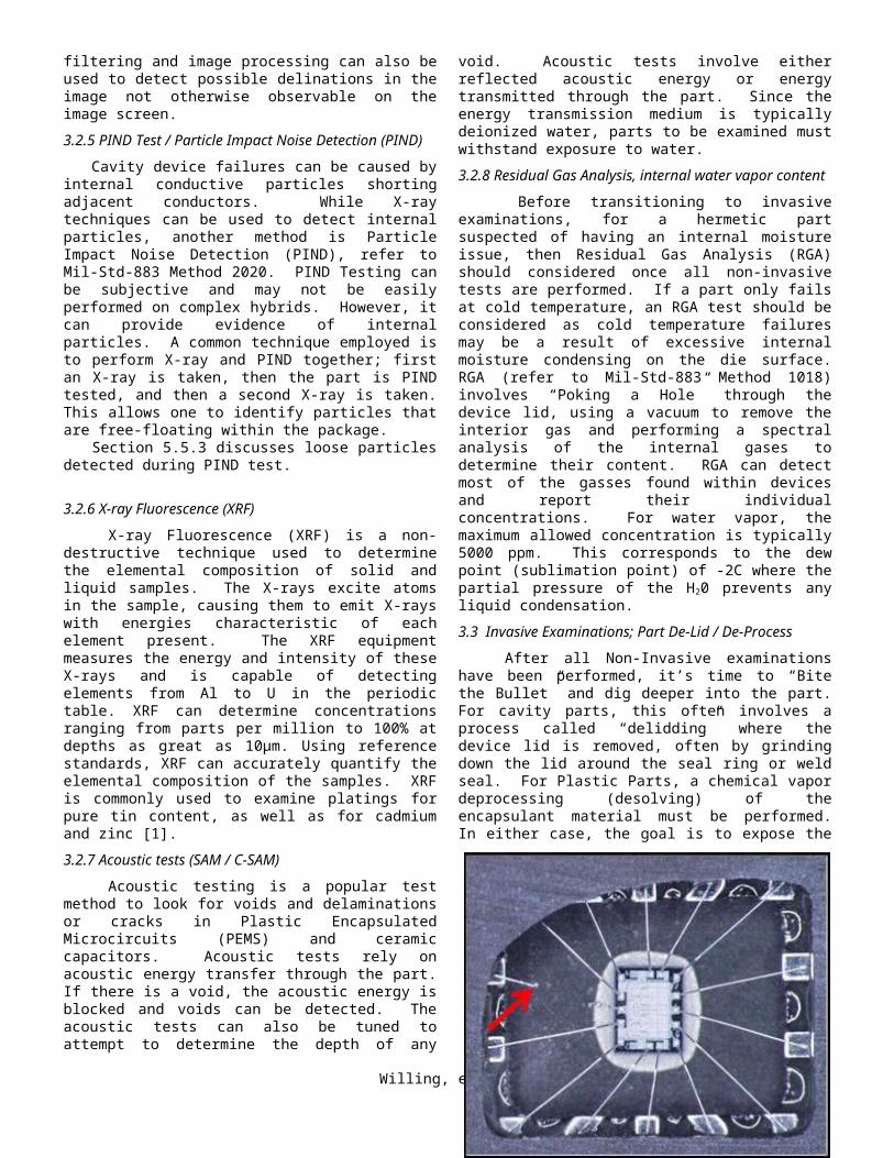
Figure 4. SEM photo of a FET gate metallization structure
3.3.7 EDS/EDX
Energy dispersive X-ray analysis, alternately known as EDS, EDAX or EDX, is a technique used along with a SEM to identify the elemental composition of a sample. During EDS, a sample is exposed to an electron beam inside the SEM. These electrons collide with the electrons within the sample, causing some of them to be knocked out of their orbits. The vacated positions are filled by higher energy electrons that emit X-rays in the process. By spectrographic analysis of the emitted X-rays, the elemental composition of the sample can be determined. EDS is a powerful tool for microanalysis of elemental constituents [2].
3.3.8 Focused Ion Beam (FIB)
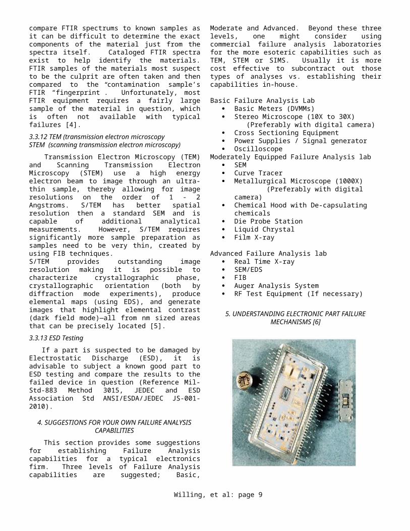
The Focused Ion Beam is a tool where an ion beam (typically a Gallium Liquid Metal Ion Source (LMIS)) is used to microscopically mil or ablate (e.g. ion milling) material away to allow for cross-sectioning of semiconductor die. Tungsten ion beams may also be used. The FIB cross-sections can be examined by Scanning Electron Microscope (SEM) to see features such as die metallization construction, pinhole in dielectrics (oxides/nitrides), any EOS, or ESD damage sites. The FIB cross sections are very “polished” revealing features at 100 Angstrom resolution. The FIB can also be used to cut semiconductor metallization lines to isolate circuitry on the die and, if necessary, a Platinum ion beam can be used to actually deposit metallization and create new circuit traces. In this case, die level design changes (known as “Device Editing”) can be implemented to allow for a design “try-out”. Figure 5 presents a FIB cross-section of a FET gate structure (see cut-out site in Figure 4).
Figure 5. FIB cross-section of a FET gate structure
(see cut-out site in Figure 4)
3.3.9 Auger Electron Spectroscopy (AES)
Auger (“O-J”) analysis is a technique where samples are exposed to an electron beam designed to dislodge secondary electrons (otherwise known as Auger electrons) from the materials being examined. The materials can be identified by the different energy level spectra unique to each material’s valence bands. Auger detection systems are useful for detecting organic materials on the surface of the die since Auger is more sensitive to lighter elements than EDS. While some depth profiling can occur, it is usually useful to 1um deep. Auger, like EDS, is an elemental technique that provides little compound information, but is most useful because it analyzes only the near surface region (~50 Angstroms analysis depth). Figure 6 presents a Auger profile of the contamination on the surface of a wire bond pad.
Figure 6. Auger profile of contamination on the surface of a wire bond pad.
SIMS is a technique that can detect very low concentrations of dopants and impurities. By ion milling deeper into the sample, SIMS can provide elemental depth profiles over a depth range from a few angstroms to tens of microns. SIMS works by sputtering the sample surface with a beam of primary ions. Secondary ions formed during sputtering are analyzed with a mass spectrometer. These secondary ions can range down to sub-parts-per-million trace levels [3]. Advanced SIMS analyses, such as Time-of-Flight SIMS (TOF-SIMS) and Dynamic SIMS (D-SIMS), provide additional means of elemental detection and resolution.
3.3.11 Fourier Transform Infrared Spectroscopy (FTIR)
Fourier Transform Infrared Spectroscopy is an analytical technique used primarily to identify organic materials, such as solder flux contamination associated with a part failure. The FTIR reveals infrared absorption spectra that provides information about the chemical bonds and molecular structure of a material. The FTIR spectrum is like a "fingerprint" of the material; however, the fingerprint itself is not like a typical spectrum with known peaks for each element. When running an FTIR analysis, it helps to compare FTIR spectrums to known samples as it can be difficult to determine the exact
Willing, et al: page 6
components of the material just from the spectra itself. Cataloged FTIR spectra exist to help identify the materials. FTIR samples of the materials most suspect to be the culprit are often taken and then compared to the contamination sample’s FTIR “fingerprint”. Unfortunately, most FTIR equipment requires a fairly large sample of the material in question, which is often not available with typical failures [4].
3.3.12 TEM (transmission electron microscopy STEM (scanning transmission electron microscopy)
Transmission Electron Microscopy (TEM) and Scanning Transmission Electron Microscopy (STEM) use a high energy electron beam to image through an ultra-thin sample, thereby allowing for image resolutions on the order of 1 - 2 Angstroms. S/TEM has better spatial resolution then a standard SEM and is capable of additional analytical measurements. However, S/TEM requires significantly more sample preparation as samples need to be very thin, created by using FIB techniques. S/TEM provides outstanding image resolution making it is possible to characterize crystallographic phase, crystallographic orientation (both by diffraction mode experiments), produce elemental maps (using EDS), and generate images that highlight elemental contrast (dark field mode)—all from nm sized areas that can be precisely located [5].
3.3.13 ESD Testing
If a part is suspected to be damaged by Electrostatic Discharge (ESD), it is advisable to subject a known good part to ESD testing and compare the results to the failed device in question (Reference Mil-Std-883 Method 3015, JEDEC and ESD Association Std ANSI/ESDA/JEDEC JS-001-2010).
4. SUGGESTIONS FOR YOUR OWN FAILURE ANALYSIS CAPABILITIES
This section provides some suggestions for establishing Failure Analysis capabilities for a typical electronics firm. Three levels of Failure Analysis capabilities are suggested; Basic, Moderate and Advanced. Beyond these three levels, one might consider using commercial failure analysis laboratories for the more esoteric capabilities such as TEM, STEM or SIMS. Usually it is more cost effective to subcontract out those types of analyses vs. establishing their capabilities in-house.
Basic Failure Analysis Lab Basic Meters (DVMMs) Stereo Microscope (10X to 30X)
(Preferably with digital camera) Cross Sectioning Equipment Power Supplies / Signal generator Oscilloscope
Moderately Equipped Failure Analysis lab SEM Curve Tracer Metallurgical Microscope (1000X)
(Preferably with digital camera)
Chemical Hood with De-capsulating chemicals Die Probe Station Liquid Chrystal Film X-ray
Advanced Failure Analysis lab Real Time X-ray SEM/EDS FIB Auger Analysis System RF Test Equipment (If necessary)
5. UNDERSTANDING ELECTRONIC PART FAILURE MECHANISMS [6]
Excerpts from the 1997 Alan O. Plait Award for Tutorial Excellence
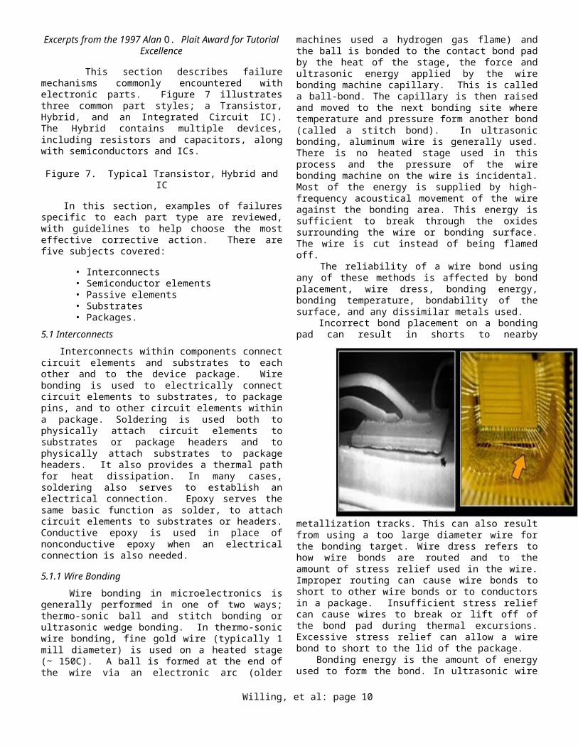
This section describes failure mechanisms commonly encountered with electronic parts. Figure 7 illustrates three common part styles; a Transistor, Hybrid, and an Integrated Circuit IC). The Hybrid contains multiple devices, including resistors and capacitors, along with semiconductors and ICs.
Figure 7. Typical Transistor, Hybrid and IC
In this section, examples of failures specific to each part type are reviewed, with guidelines to help choose the most effective corrective action. There are five subjects covered:
• Interconnects• Semiconductor elements• Passive elements• Substrates• Packages.
5.1 Interconnects
Interconnects within components connect circuit elements and substrates to each other and to the device package. Wire bonding is used to electrically connect circuit elements to substrates, to package pins, and to other circuit elements within
Willing, et al: page 7
a package. Soldering is used both to physically attach circuit elements to substrates or package headers and to physically attach substrates to package headers. It also provides a thermal path for heat dissipation. In many cases, soldering also serves to establish an electrical connection. Epoxy serves the same basic function as solder, to attach circuit elements to substrates or headers. Conductive epoxy is used in place of nonconductive epoxy when an electrical connection is also needed.
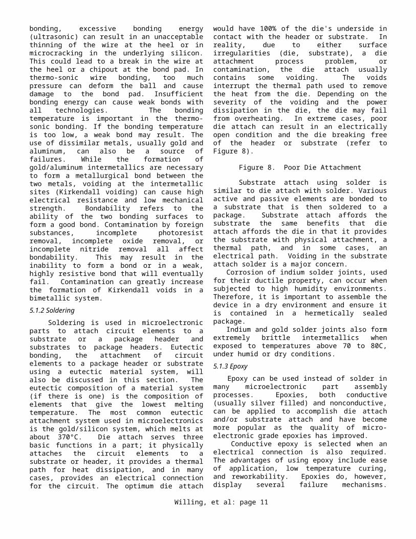
5.1.1 Wire Bonding
Wire bonding in microelectronics is generally performed in one of two ways; thermo-sonic ball and stitch bonding or ultrasonic wedge bonding. In thermo-sonic wire bonding, fine gold wire (typically 1 mill diameter) is used on a heated stage (~ 150C). A ball is formed at the end of the wire via an electronic arc (older machines used a hydrogen gas flame) and the ball is bonded to the contact bond pad by the heat of the stage, the force and ultrasonic energy applied by the wire bonding machine capillary. This is called a ball-bond. The capillary is then raised and moved to the next bonding site where temperature and pressure form another bond (called a stitch bond). In ultrasonic bonding, aluminum wire is generally used. There is no heated stage used in this process and the pressure of the wire bonding machine on the wire is incidental. Most of the energy is supplied by high-frequency acoustical movement of the wire against the bonding area. This energy is sufficient to break through the oxides surrounding the wire or bonding surface. The wire is cut instead of being flamed off. The reliability of a wire bond using any of these methods is affected by bond placement, wire dress, bonding energy, bonding temperature, bondability of the surface, and any dissimilar metals used. Incorrect bond placement on a bonding pad can result in shorts to nearby metallization tracks. This can also result from using a too large diameter wire for the bonding target. Wire dress refers to how wire bonds are routed and to the amount of stress relief used in the wire. Improper routing can cause wire bonds to short to other wire bonds or to conductors in a package. Insufficient stress relief can cause wires to break or lift off of the bond pad during thermal excursions. Excessive stress relief can allow a wire bond to short to the lid of the package. Bonding energy is the amount of energy used to form the bond. In ultrasonic wire bonding, excessive bonding energy (ultrasonic) can result in an unacceptable thinning of the wire at the heel or in microcracking in the underlying silicon. This could lead to a break in the wire at the heel or a chipout at the bond pad. In thermo-sonic wire bonding, too much pressure can deform the ball and cause damage to the bond pad. Insufficient bonding energy can cause weak bonds with all technologies. The bonding temperature is important in the thermo-sonic bonding. If the bonding temperature is too low, a weak bond may result. The use of dissimilar metals, usually gold and aluminum, can also be a source of failures. While the formation of gold/aluminum intermetallics are necessary to
form a metallurgical bond between the two metals, voiding at the intermetallic sites (Kirkendall voiding) can cause high electrical resistance and low mechanical strength. Bondability refers to the ability of the two bonding surfaces to form a good bond. Contamination by foreign substances, incomplete photoresist removal, incomplete oxide removal, or incomplete nitride removal all affect bondability. This may result in the inability to form a bond or in a weak, highly resistive bond that will eventually fail. Contamination can greatly increase the formation of Kirkendall voids in a bimetallic system.
5.1.2 Soldering
Soldering is used in microelectronic parts to attach circuit elements to a substrate or a package header and substrates to package headers. Eutectic bonding, the attachment of circuit elements to a package header or substrate using a eutectic material system, will also be discussed in this section. The eutectic composition of a material system (if there is one) is the composition of elements that give the lowest melting temperature. The most common eutectic attachment system used in microelectronics is the gold/silicon system, which melts at about 370°C. Die attach serves three basic functions in a part; it physically attaches the circuit elements to a substrate or header, it provides a thermal path for heat dissipation, and in many cases, provides an electrical connection for the circuit. The optimum die attach would have 100% of the die's underside in contact with the header or substrate. In reality, due to either surface irregularities (die, substrate), a die attachment process problem, or contamination, the die attach usually contains some voiding. The voids interrupt the thermal path used to remove the heat from the die. Depending on the severity of the voiding and the power dissipation in the die, the die may fail from overheating. In extreme cases, poor die attach can result in an electrically open condition and the die breaking free of the header or substrate (refer to Figure 8).
Figure 8. Poor Die Attachment
Substrate attach using solder is similar to die attach with solder. Various active and passive elements are bonded to a substrate that is then soldered to a package. Substrate attach
Willing, et al: page 8
affords the substrate the same benefits that die attach affords the die in that it provides the substrate with physical attachment, a thermal path, and in some cases, an electrical path. Voiding in the substrate attach solder is a major concern. Corrosion of indium solder joints, used for their ductile property, can occur when subjected to high humidity environments. Therefore, it is important to assemble the device in a dry environment and ensure it is contained in a hermetically sealed package. Indium and gold solder joints also form extremely brittle intermetallics when exposed to temperatures above 70 to 80C, under humid or dry conditions.
5.1.3 Epoxy
Epoxy can be used instead of solder in many microelectronic part assembly processes. Epoxies, both conductive (usually silver filled) and nonconductive, can be applied to accomplish die attach and/or substrate attach and have become more popular as the quality of micro-electronic grade epoxies has improved. Conductive epoxy is selected when an electrical connection is also required. The advantages of using epoxy include ease of application, low temperature curing, and reworkability. Epoxies do, however, display several failure mechanisms. Improperly cured epoxy can outgas inside a hermetic package after it has been sealed, releasing moisture and ionic contaminants into the internal cavity of the package. Because of their inherent charge, these ionic contaminants may shift the electrical parameters of electronic devices in the package. This is of particular concern when Metal Oxide Semiconductor (MOS) devices are present. Adhesive ionic contaminant issues can be mitigated by selecting epoxies that meet Mil-Std-883 Method 5011 requirements. Poor adhesion of an epoxy to either the die or the substrate is another failure mechanism for epoxy. This type of failure is usually caused by improper cleaning or abrading of either joining surface. If stable electrical resistance of the attachment is critical to circuit performance, conductive epoxy may not be the best choice as earlier formulations exhibited changes in the electrical resistance over time. It can also be affected by factors such as temperature and humidity. Electrolytic corrosion can occur in silver filled conductive epoxy when sufficient moisture is present in a package. The silver from the epoxy is corroded by the moisture and by other substances in the epoxy. It can then be transported under the influence of an electric field in the package and cause shorting to adjacent metallization tracks or components.
5.2 Semiconductor Elements
Semiconductor elements include discrete diodes, discrete transistors, and integrated circuits. The semiconductor elements can be packaged individually or grouped together in a hybrid configuration. Semiconductor element failures can be broken down into the three categories of metallization failures; oxide failures, and failures induced by overstress.
5.2.1 Metallization
Metallization on a semiconductor element is a thin film pattern of metal deposited on a chip to connect electronic components contained on the chip or to establish contacts that may be connected externally. Metallization failures generally result in electrical opens, although shorts may also be experienced. Metallization failures can be divided into the following specific categories; step coverage, electromigration, misalignment, corrosion, mechanical damage, and stress voiding. Step coverage on a semiconductor element refers to the thickness of a material deposited on an area with an uneven topography. A change in the vertical direction is called a step. Thinning in the metallization (usually aluminum) over a step is allowed to reduce to 50% of the metal thickness over a flat area. If step coverage is poor (less than 50%), open circuits can result. Modern IC’s have multilayer planarized metallization which eliminates many of the step issues. Electromigration of metal results in an open circuit condition. Electromigration is caused by a thermal activation of aluminum ions that are physically moved by momentum exchange with flowing electrons. Electromigration failures are a function of the current density in an aluminum conductor and its temperature. Usually, design rules preclude this current density from being exceeded. Mil-Prf-38535, for example, specifies that the current density for glassivated aluminum metallization shall not exceed 5x10⁵ A/cm2 for case operating temperatures up to 125°C. Defects in the metallization, such as poor step coverage or voiding, can allow localized areas of current constriction to occur. Misapplication of a device in a circuit can also lead to excessive current densities. Misaligned metallization on an integrated circuit can result in poor contact to active circuit elements or to other metallization levels. This type of defect is caused by poorly aligned masks during fabrication. Failures in the form of opens can result from this defect. Corrosion of aluminum metallization is another failure mechanism. Corrosion can occur due to the introduction of contaminants during processing or due to moisture penetrating into the cavity of a non-hermetic package. Aluminum bond pads are especially susceptible because they are not passivated. Corrosion can also occur if moisture is inadvertently sealed in a hermetic package. Mechanical damage to metallization can be introduced during probing or handling. This is especially true in hybrid microcircuits, which are exposed to a large number of assembly steps. Mechanical damage to metallization can result in shorts or opens. Stress voiding is a relatively new failure mechanism that has been identified. Voids form in the aluminum metallization on an integrated circuit due to a tensile stress that is exerted on it by the passivation. The voids tend to occur at aluminum grain boundaries. Void formation is highly dependent on device geometry, processing, and the particular metallization system used.
5.2.2 Overstress
Willing, et al: page 9
Overstress refers to the application of voltage or current, or a combination of the two (power), to a device that exceeds its capabilities. Irreversible damage can result in the metallization, oxide, semiconductor material, etc. Overstresses can be divided into two basic groups: electrical overstress (EOS) and electrostatic discharge (ESD). Electrical overstress is one of the most common causes of failure for an electronic device. It can be a continuous event or it can be transient in nature. An EOS failure can be caused by the failure of another device in a circuit, the misapplication of a device in a circuit, or the external application of excessive power to a device. One of the most challenging aspects of failure analysis can be to determine whether a device failed from an internal defect or an external overstress. The damage that results from EOS can range from the leakage of a single gate in a Very Large Scale Integration (VLSI) device to the fusing of a discrete power transistor. Electrostatic discharge is the transfer of charge between two bodies that are at different potentials. Semiconductor elements are sensitive to ESD. Sources of static for ESD include work surfaces, plastic bags, and the human body. The ESD event itself is a transient phenomenon. It can be modeled as a capacitor discharging through a resistor. Generally, semiconductor elements exposed to sufficiently high levels of ESD will experience varying degrees of damage. Many times ESD damage is very subtle. This is because the ESD event is very short in duration, usually about 200 nanoseconds when the source is a human body. The control of ESD is now itself an industry that supports electronics manufacturers.
5.2.3 Oxides / Nitrides
Oxides (silicon dioxide) and Nitrides (silicon nitride) serve to provide an insulating barrier between conductors or between semiconductors and conductors. They are also used as a passivation layer to protect the underlying structures. Oxides can be deposited on a silicon chip or can be thermally grown. There are three oxide/nitride failure mechanisms that will be discussed here: ionic impurities, oxide defects, and hot carrier effects. Ionic impurities can contaminate the oxide/nitride and affect device operation, particularly in MOS devices. Sodium ions, which are highly mobile in oxide, were a common impurity found in early semiconductor processes. These ions, when affected by an electrical bias, can migrate in the oxide and cause degraded device operation or failure. Generally these “Mobile Ion” failure mechanisms have been eliminated from semiconductor processing. However, if they should occur, stressing the oxide with the appropriate voltage can screen out such devices. Another failure mechanism caused by ion migration in oxide is time dependent dielectric breakdown, and it is not as easily screened out. In this case, the ions are emitted into the oxide from a gate metal during the operation of the device. Again, degraded performance or failure can result. There are design criteria that are used to limit this phenomenon. Physical defects in an oxide can cause failure, particularly in the thin gate oxides of MOS devices. Pin holes in the oxide can
reduce its dielectric strength and result in breakdown. Severely thinned oxides can also reduce dielectric strength and cause breakdown. Hot carrier electrons can cause failures in integrated circuits. Hot carrier electrons are very energetic electrons which can affect the oxide by forming trapped charge regions, resulting in device failure. They are more troublesome in small geometry devices (found it VLSI devices), where geometries are shrunk but operating voltages (usually + 3.3 volts, down to +1.0 volts) are held constant. Unique VLSI processing techniques can leave subtly damaged oxide which may result in more trapped charges.
5.3 Passive Elements
Passive elements used in microelectronics include resistors and capacitors. There are many different types of capacitors to choose from. Ceramic capacitors are probably the most common style of capacitor used. When a large amount of capacitance is required in a small volume, tantalum is usually the choice. Resistors can be produced by both thick film and thin film technologies.
5.3.1 Capacitors
Ceramic capacitors are named for their ceramic dielectric material. They generally have two sets of interleaved plating to increase the area of the plates and thereby increase their capacitance. End caps are added to join the two sets of plates. One of the most common failure modes for ceramic capacitors occurs during their soldering to substrates or boards. The thermal shock associated with the soldering of the capacitors can cause the ceramic to crack. If the crack extends between plates of opposite polarity, the device's dielectric breakdown voltage will drop off and the device will short when voltage is applied to it. Barrier metals must be used on end caps so that solder leaching will not occur. Tantalum capacitors use tantalum pentoxide as a dielectric. Their typical failure mode involves cracked connections.
5.3.2 Resistors
The term thick film resistor refers to the way the resistor was fabricated. Thick film technology is a field of microelectronics in which special pastes are silk-screened onto a ceramic substrate and then fired at high temperature to bond the films to the substrate. Thick film resistors are widely used in hybrids. Failure mechanisms include poor adhesion and EOS. Thin film resistors are fabricated utilizing thin film technology. Thin film technology refers to the deposition of a material (usually less than 5 microns in thickness) onto a substrate by vacuum deposition or sputtering. Failure modes include poor adhesion, cracking, EOS, and, ESD due to their thin film nature.
5.4 Substrates
Substrates are used in microelectronics, particularly when manufacturing hybrids, to mount circuit elements onto and to make electrical interconnections. Substrates, typically formed out of a ceramic material, save space inside a package and
Willing, et al: page 10
reduce its weight. Substrates can fail from several different mechanisms as discussed below.
5.4.1 Cracking
Cracking in a substrate can cause a failure if the substrate crack propagates through a metallization stripe. A crack in a substrate can also propagate through an attached component (a die, for example) causing the component to fail. Cracks in a substrate can be caused by a thermal coefficient of expansion mismatch between a substrate and a package header. They can also be introduced by mechanical damage.
5.4.2 Metallization
Metallization failures, which were shown to occur on semiconductor die, also occur on substrates. Lifting of the metallization from the substrate can occur, usually resulting from an improperly cleaned substrate prior to metallization application. Poor metallization coverage is also a failure mechanism. Leaching of gold metallization into solders can also occur if the proper barrier metals are not used.
5.4.3 Multilayer Substrates
Multilayer substrates (substrates with two or more levels of metallization) suffer from the same failure mechanisms as single layer substrates, with two additions. Incomplete via fills (a via is an internal connection between two metallization layers) occur during substrate fabrication and result in open circuits. Shorts between metallization layers also happen during substrate fabrication.
5.5 Packages
Packages physically protect circuit elements from the external environment. They also allow for electrical connection to other packages in an electrical system. The failure of a package to protect its internal components from the external environment can result in device failure. Package failures can be classified as hermeticity failures, insulation resistance failures, or failures caused by loose particles within the package.
5.5.1 Hermeticity
Microelectronics packages are either hermetic or nonhermetic. Hermetic packages effectively seal the internal components from the external atmosphere. Nonhermetic packages (plastic packages) allow outside air to penetrate the package. Moisture can lead to many forms of corrosion inside a package and is one of the most important contaminants to seal out. Hermetic seals require the use of some combination of metal. glass, and/or ceramic in the package seal. Devices that fail hermeticity are referred to as fine leakers or gross leakers. A fine leak is defined as a leak rate that is greater than 1 x 10⁻⁷ atm cc/sec (however this rate does depend on the package volume). A gross leak is any leak rate greater than 1 x 10⁻⁵
atm cc/sec, usually detectable by looking for bubbles from a package while immersed in a hot fluorocarbon.
5.5.2 Insulation Resistance
Insulation resistance between package pins and leads must be maintained for a device to function properly. Contamination on the exterior of a package can cause the insulation resistance to fail. Leaching of lead from the glass sealing material has historically caused insulation resistance failures.
5.5.3 Loose Particles
Loose particles inside a package can cause a failure. This is especially true if the particles are conductive. A loose conductive particle in a package can cause a failure by creating a short between other conductors inside the package. Particle Impact Noise Detection (PIND) testing is used to detect loose particles inside a package. Radiographic examination can then be used to verify the size and density of the particle before the device is delidded.
6. FAILURE ANALYSIS CASE STUDY
This section discusses the failure analysis performed on a hermetically packaged integrated circuit (multiplexer). The failure was caused by corrosion within the package. This example presents the types of problems that are encountered and how proper failure analysis can help implement effective corrective action.
6.1 Mux Failure Analysis
A multiplexer Integrated Circuit (Mux IC) failure was first discovered during a system level electrical test. The microcircuit used a standard high reliability package design consisting of a ceramic housing with a hermetic seal. Prior to the failure, the multiplexer was exposed to multiple temperature performance and environmental screening tests at the component and board level assembly. It was not until integration at a higher level assembly that an anomaly arose. The initial trouble shooting quickly isolated the problem to the multiplexer. At the time, the anomalous behavior was seen only during electrical testing below 0°C. After careful assessment of the part as installed on the board, it was removed for further investigation. The part was photographed and leak checked as a normal course of action. It passed the fine and gross leak check. The part was then retested electrically at low temperature to demonstrate the issue was reproducible at the component level. The next step was performing real-time X-ray, which observed a possible open circuit, refer to figure 9. After exhibiting similar anomalous behavior it was delidded for internal inspection. The inspection revealed signification corrosion; refer to figure 10. The corrosion primarily attacked the wire bond for Vcc which brings in external DC power. The interconnect was degraded to the point of being intermittent over temperature. The cause of corrosion is typically due to moisture trapped in packages prior to seal. Moisture can react with residual plating salts and cause significant corrosion between
Willing, et al: page 11
interconnecting joints especially in presence of an electrical field.
Figure 9. Real-time X-ray of Multiplexer IC Revealed Possible Corrosion
Figure 10. Multiplexer IC After Lid Removal revealing corrosion on Pin 13
Military-Standard packages require Residual Gas Analysis Test (RGA) as a qualification for low moisture content (i.e. <5,000 ppmv). The records showed the lot of devices passed qualification. High moisture content is commonly due to an inadequate bake out and sealing process though other possibilities exist. Since the device passed leak testing prior to lid removal, it indicates the moisture was trapped in the device prior to seal.
6.2 Corrective action
Given that the device was advertised as space grade high reliability, the vendor was contacted and an on-site review was conducted. In addition, five devices from the same lot were checked for moisture via the RGA test procedure and then delidded for inspection. They all passed the RGA tests as well as the inspection. Given the overall findings and positive on site review, the rest of the lot was ultimately exonerated and the failure was classified as an isolated issue.
7. CONCLUSIONS
It is the goal of this tutorial that the audience has gained a good understanding of the failure analysis process and the tools and techniques available for performing failure analysis on electronic components. The authors hope this goal has been achieved. The authors would like to acknowledge all of the past and present Failure Analysis Engineers at Northrop Grumman Electronic systems for their contributions to this tutorial, notably, Richard Brooks, John Knepley, Robert Pearson, Randall Lewis and Ronald Twist.
8. REFERENCES
1. Evans Analytical Group, http://www.eaglabs.com/2. Evans Analytical Group, http://www.eaglabs.com/3. Evans Analytical Group, http://www.eaglabs.com/4. Evans Analytical Group, http://www.eaglabs.com/5. Evans Analytical Group, http://www.eaglabs.com/6. Knepley, John, W., “Understanding Electronic Part Failure
Mechanisms”, Tutorial Notes, 1998 Annual Reliability and Maintainability Symposium, (Jan) 1998.
8.1 Industry Standards
ANSI/ESDA/JEDEC JS-001-2010, “Electrostatic Discharge Sensitivity Testing Human Body Model (HBM) - Component Level”
8.2 Military Standards
Mil-Std-883H; “Test Method Standard Microcircuits” 26 February 2010
Mil-Std-1580B; “Destructive Physical Analysis For Electronic, Electromagnetic, And Electromechanical Parts”, 15 November 2010
Mil-Prf-38535J; “Integrated Circuits (Microcircuits) Manufacturing, General Specification For”, 28 December 2010
Willing, et al: page 12