AN1325: Choosing and Using Bypass Capacitors
11
Choosing and Using Bypass Capacitors APPLICATION NOTE AN1325 Rev 1.00 Page 1 of 11 Oct 10, 2011 AN1325 Rev 1.00 Oct 10, 2011 Introduction Bypass capacitors are found in every working piece of electronic equipment. Most engineers know that systems, circuits, and individual chips need to be bypassed. The methods for choosing bypass capacitors typically follow decisions of tradition instead of optimizing for any particular circuit. This application note aims to bring the design aspect back to this seemingly simple component. After discussing the motivation for using bypass caps, we form a vocabulary around the basics; equivalent circuit, dielectrics and types of available capacitors. The next step is identifying the primary function and environment of the bypass capacitor. Circuits that exhibit large current spikes have different bypassing needs than ones that solely operate at high frequencies. A few special options are discussed, like scaling multiple bypass capacitors, as well as the importance of board layout. Finally, we present four application examples. These represent circuits with high and low currents as well as those with high and low frequencies. Motivation It’s far too common (and quite distressing) to breadboard a circuit in an ideal configuration; only to find that it doesn’t work well or it doesn’t work at all (Figure 1). Noise may have coupled into the circuit from the power supply, internal IC circuitry, or nearby IC. Wires and board connections act like antennas and power supply levels change with current draw. Taking a look at the power supply pin on the oscilloscope shows the following result (Figure 2). . As one can see, there is a lot of high frequency noise displacing the DC level (approximately 10mV P-P ). Then, far more pronounced, there are regular spikes in excess of 50mV. Since power supplies are assumed to be stable (constant DC voltage), any perturbations will couple directly into the circuit and get to the output depending on the PSRR. The first line of defense against unwanted perturbations on the power supply is the bypass capacitor. A bypass capacitor eliminates voltage droops on the power supply by storing electric charge to be released when a voltage spike occurs. It also provides this service at a wide range of frequencies by creating a low-impedance path to ground for the power supply. We have four questions to answer before grabbing the closest capacitor: 1. What size bypass capacitor do we need? 2. Where do we place the bypass capacitor for maximum effect? 3. What type of bypass capacitor will work best/adequately in our circuit/system? 4. And a hidden fourth question—what type of package do I need to choose for my bypass capacitor? (which will depend on the size needed, the board area available, and type of capacitor chosen) The simplest question to answer is #2, placement. A bypass capacitor should be placed as close as possible to the power supply pin of each chip. Any extra distance translates into additional series inductance, which lowers the self-resonant frequency (useful bandwidth) of the bypass capacitor. FIGURE 1. BREADBOARDED NON-INVERTING AMPLIFIER CONFIGURATION (A V = 2) 5V GND RF RG OUT IN OUT IN RF RG + - FIGURE 2. OSCILLOSCOPE VIEW OF DC POWER SUPPLY PIN ON NON-INVERTING AMPLIFIER
Transcript of AN1325: Choosing and Using Bypass Capacitors
Choosing and Using Bypass Capacitors
APPLICATION NOTE
AN1325 Rev 1.00Oct 10, 2011
AN1325
Rev 1.00Oct 10, 2011
IntroductionBypass capacitors are found in every working piece of electronic equipment. Most engineers know that systems, circuits, and individual chips need to be bypassed. The methods for choosing bypass capacitors typically follow decisions of tradition instead of optimizing for any particular circuit. This application note aims to bring the design aspect back to this seemingly simple component. After discussing the motivation for using bypass caps, we form a vocabulary around the basics; equivalent circuit, dielectrics and types of available capacitors.
The next step is identifying the primary function and environment of the bypass capacitor. Circuits that exhibit large current spikes have different bypassing needs than ones that solely operate at high frequencies. A few special options are discussed, like scaling multiple bypass capacitors, as well as the importance of board layout.
Finally, we present four application examples. These represent circuits with high and low currents as well as those with high and low frequencies.
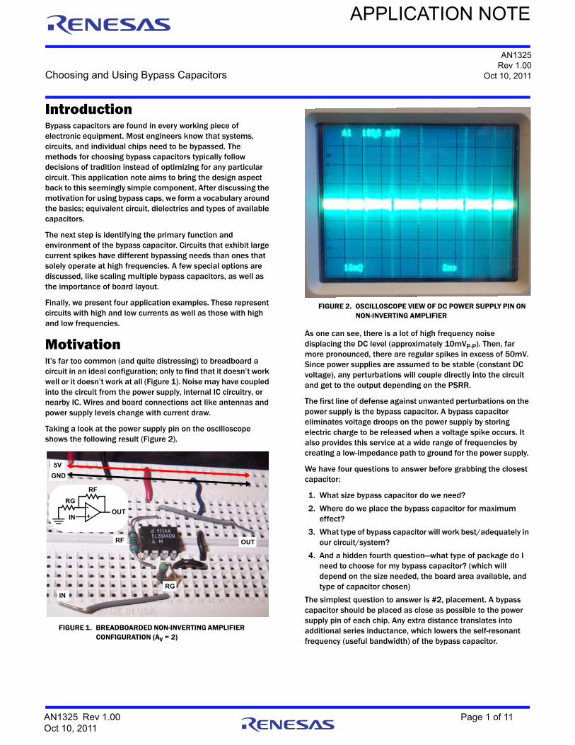
MotivationIt’s far too common (and quite distressing) to breadboard a circuit in an ideal configuration; only to find that it doesn’t work well or it doesn’t work at all (Figure 1). Noise may have coupled into the circuit from the power supply, internal IC circuitry, or nearby IC. Wires and board connections act like antennas and power supply levels change with current draw.
Taking a look at the power supply pin on the oscilloscope shows the following result (Figure 2).
.
As one can see, there is a lot of high frequency noise displacing the DC level (approximately 10mVP-P). Then, far more pronounced, there are regular spikes in excess of 50mV. Since power supplies are assumed to be stable (constant DC voltage), any perturbations will couple directly into the circuit and get to the output depending on the PSRR.
The first line of defense against unwanted perturbations on the power supply is the bypass capacitor. A bypass capacitor eliminates voltage droops on the power supply by storing electric charge to be released when a voltage spike occurs. It also provides this service at a wide range of frequencies by creating a low-impedance path to ground for the power supply.
We have four questions to answer before grabbing the closest capacitor:
1. What size bypass capacitor do we need?
2. Where do we place the bypass capacitor for maximum effect?
3. What type of bypass capacitor will work best/adequately in our circuit/system?
4. And a hidden fourth question—what type of package do I need to choose for my bypass capacitor? (which will depend on the size needed, the board area available, and type of capacitor chosen)
The simplest question to answer is #2, placement. A bypass capacitor should be placed as close as possible to the power supply pin of each chip. Any extra distance translates into additional series inductance, which lowers the self-resonant frequency (useful bandwidth) of the bypass capacitor.
FIGURE 1. BREADBOARDED NON-INVERTING AMPLIFIER CONFIGURATION (AV = 2)
5V
GND
RF
RG
OUT
IN
OUTIN
RF
RG
+
-
FIGURE 2. OSCILLOSCOPE VIEW OF DC POWER SUPPLY PIN ON NON-INVERTING AMPLIFIER
Page 1 of 11
Choosing and Using Bypass Capacitors
The effect of the bypass capacitor on the output of the non-inverting amplifier can be seen in Figure 4.
Further improvements in dealing with the placement and routing of the bypass capacitor will involve discussion of printed circuit board design—the topic of our next in-depth discussion.
The other three questions (about capacitor size, type, and package choice) are the heart of this discussion. These topics will be discussed in detail after first reviewing capacitor basics.
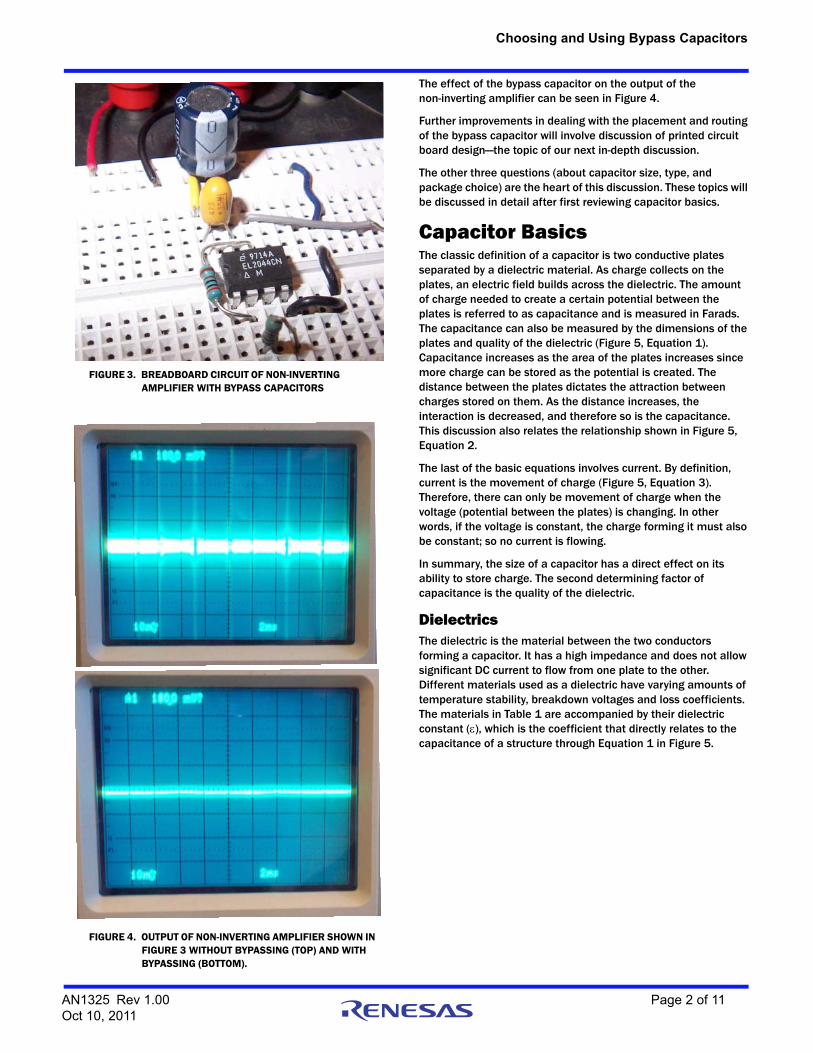
Capacitor BasicsThe classic definition of a capacitor is two conductive plates separated by a dielectric material. As charge collects on the plates, an electric field builds across the dielectric. The amount of charge needed to create a certain potential between the plates is referred to as capacitance and is measured in Farads. The capacitance can also be measured by the dimensions of the plates and quality of the dielectric (Figure 5, Equation 1). Capacitance increases as the area of the plates increases since more charge can be stored as the potential is created. The distance between the plates dictates the attraction between charges stored on them. As the distance increases, the interaction is decreased, and therefore so is the capacitance. This discussion also relates the relationship shown in Figure 5, Equation 2.
The last of the basic equations involves current. By definition, current is the movement of charge (Figure 5, Equation 3). Therefore, there can only be movement of charge when the voltage (potential between the plates) is changing. In other words, if the voltage is constant, the charge forming it must also be constant; so no current is flowing.
In summary, the size of a capacitor has a direct effect on its ability to store charge. The second determining factor of capacitance is the quality of the dielectric.
DielectricsThe dielectric is the material between the two conductors forming a capacitor. It has a high impedance and does not allow significant DC current to flow from one plate to the other. Different materials used as a dielectric have varying amounts of temperature stability, breakdown voltages and loss coefficients. The materials in Table 1 are accompanied by their dielectric constant (), which is the coefficient that directly relates to the capacitance of a structure through Equation 1 in Figure 5.
FIGURE 3. BREADBOARD CIRCUIT OF NON-INVERTING AMPLIFIER WITH BYPASS CAPACITORS
FIGURE 4. OUTPUT OF NON-INVERTING AMPLIFIER SHOWN IN FIGURE 3 WITHOUT BYPASSING (TOP) AND WITH BYPASSING (BOTTOM).
AN1325 Rev 1.00 Page 2 of 11Oct 10, 2011
Choosing and Using Bypass Capacitors
Equivalent Circuit ModelOnce the structure is understood, the next logical step is creating an equivalent circuit model to use in simulation. The equivalent circuit model is shown in Figure 6. The main component, the capacitance, has a leakage resistance in parallel with it to represent any losses through the dielectric. In series with that RC pair is another resistive term in addition to an inductive term. These two values (ESR and ESL) represent the entire amount of DC and frequency dependent losses of the capacitive structure. Again, capacitor type and structure will dictate the values of these parasitic components.
V =
CAPACITANCE
VOLTAGE B/T PLATES
CHARGE ON PLATE
Q
C
(2)
CAPACITANCE
CURRENT
CHANGE IN VOLTAGE PER UNIT TIME
dV
dT
(3) I = C
TOP PLATE
BOTTOM PLATE
DIELECTRIC
I = DQ
DT
BY DEFINITION:
C (IN FARADS) =
AREA OF PLATE
DISTANCE B/T PLATES
DIELECTRIC CONSTANT
(1)
A
D
FIGURE 5. CAPACITOR STRUCTURE AND BASIC EQUATIONS
(EQ. 1)
(EQ. 2)
(EQ. 3)
FIGURE 6. EQUIVALENT CIRCUIT MODEL WITH COMPONENT DESCRIPTION
ABBREVIATION EXPLANATION SOURCE AND DETAILSESR Equivalent Series
ResistanceWire and connections to the plateProduces heat
ESL Equivalent Series Inductance
Depends on package typeSurface mount betterSmaller SMD better
RLEAK Leakage Resistance Type of dielectric
ESR
ESL
RLEAKC
TABLE 1. EXAMPLES OF DIELECTRIC MATERIALS AND THEIR DIELECTRIC CONSTANTS
DIELECTRIC CONSTANT OF MATERIALS
Air 1.00
Alsimag 196 5.70
Bakelite 4.90
Cellulose 3.70
Fiber 6.00
Formica 1.75
Glass 7.75
Mica 5.10
Mycalex 7.10
Paper 3.00
Plexiglass 2.80
Polyethylene 2.30
Polystyrene 2.60
Porcelain 5.57
Pyrex 4.00
Quartz 3.80
Steatite 5.80
Teflon 2.10
AN1325 Rev 1.00 Page 3 of 11Oct 10, 2011

Choosing and Using Bypass Capacitors
Common Types of Capacitors and Trade-offsAs described in the previous sections, the materials and structure of a capacitor will dictate its attributes, like parasitics, temperature stability, maximum voltage, linearity, cost and size. A summary of the most popular capacitors available in surface mount packages is given in Table 2.
Ceramic capacitors are the most common capacitor type since they are inexpensive, offer a wide range of values, and provide solid performance. Tantalum, OSCON, and Aluminum Electrolytic capacitors are all polarized (specifically to be used as a bypass capacitor). Tantalum found their niche in low-voltage systems. Aluminum electrolytic capacitors are a common choice for low-to-medium frequency systems, but not switching circuits (they hold their charge too well which doesn’t suit them for the rapid cycling of production testing). OSCON is a special capacitor type developed to provide low parasitics, wide frequency range and full temperature range (the best quality available for the highest price tag). If you have the budget, these capacitors will provide quality bypass for any circuit.
Mica and Plastic Film capacitors are included for completeness. Their primary use is in filter design instead of bypass.
Since ceramic capacitors are the most widely used bypass capacitors, it is useful to look at the options available in purchasing. As expected, ceramic caps are available in a wide range of values and in a wide variety of packages. Within these parameters, there are further choices which will determine the final price. An example is set forth in Table 3. In a recent bill of materials, the capacitors were labeled as “X7R”. The X and 7 set the widest temperature range. The final letter “R” reports the tolerance of that capacitor over the temperature range. In this case, there would only be a 15% change in capacitor vs temperature. A wider temperature range and tighter tolerance earn higher price tags.
TABLE 2. COMMON CAPACITOR SPECIFICATIONS AND TRADE-OFFS
TYPE PIC CAP RANGE ESR LEAKAGE VOLTAGE RATING TEMP RANGE GENERAL NOTES
Ceramic pF to µF Low Medium High -55°C to +125°C Multipurpose Cheap
Mica(silver mica)
pF to nF Low0.01 to 0.1
Low High -55°C to +125°C For RF FiltersExpensiveVery Stable
Plastic Film(polyethylene polystyrene)
few µFs Medium Medium High Varies For Low FrequencyInexpensive
Tantalum µFs High0.5 to 5.0
Low Lowest -55°C to +125°C ExpensiveNonlinear (bad for audio)
OSCON µFs Low0.01 to 0.5
Low Low -55°C to +105°C Best QualityHighest Price
Aluminum Electrolytic
HighµFs
High0.05 to 2.0
Medium Low For Low to Med. FrequenciesInexpensiveHold Charge for Long Time - Not for Production Test
AN1325 Rev 1.00 Page 4 of 11Oct 10, 2011

Choosing and Using Bypass Capacitors
Selecting the Package for the Bypass CapacitorOnce the dielectric material, dielectric quality, temperature range, acceptable leakage and voltage range have been met, the final choice involves package dimensions. Typically, the package size is chosen by “what was used last time” or what is big enough to solder by hand (if a prototype).
What you need to remember is that the equivalent circuit model will change with different packages. The main issue is the equivalent series inductance (ESL). Obviously, a capacitor structure is constant as long as the capacitance value is constant. If that same capacitor is available in a variety of packages, then the connections between the plates and the outer dimensions of the package must change. This appears as additional series resistance and series inductance. The smaller the package is, the smaller the series parasitics. To demonstrate this trend, Table 4 is included. As expected, the effective series inductance decreases monotonically as package size decreases. Special attention should be paid to the 1206 and 0612 case. Although they have the same footprint, the 1206 has connections on the ends while the 0612 has connections on the longer edges. This simple change in orientation allows the inner package connections to be much smaller. Delightfully, the ESL is reduced by 95%. In wide bandwidth circuits, the amount of series inductance sets an upper bound on the ability of the bypass circuit to provide a low impedance for the power supply pin. This will be further discussed in the following sections.
Sizing Bypass CapacitorsBypass capacitors are usually sized by convention or typical values. For example, common values are 1µF and 0.1µF. In the simplest terms, the larger value handles the lower frequencies and high current issues while the smaller value handles higher frequencies. The need for multiple capacitors comes from the parasitics associated with real capacitors.
TABLE 3. CLASSIFICATION OF CERAMIC CAPACITOR OPTIONS
CERAMIC (EIA CLASS II) CAPACITOR CODE
LETTER SYMBOL LOW TEMP. REQUIREMENT NUMBER SYMBOL HIGH TEMP. REQUIREMENT LETTER SYMBOL MAX. C OVER T
Z +10°C 2 +45°C A ±1.0%
B ±1.5%
4 +65°C C ±2.2%
Y -30°C D ±3.3%
5 +85°C E ±4.7%
F ±7.5%
X -55°C 6 +105°C P ±10.0%
R ±15.0%
7 +125°C S ±22.0 -
T ±22.0 -
U ±22.0 -
V ±22.0 -
TABLE 4. SURFACE MOUNT PACKAGES AND THEIR EQUIVALENT SERIES INDUCTANCES
PACKAGE ESL (pH)
0201 400
0402 550
0603 700
0805 800
1206 1250
0612 63
FIGURE 7. EXAMPLE SURFACE MOUNT PACKAGES IN THE 1206 ORIENTATION (TOP) AND THE 0612 ORIENTATION (BOTTOM)
AN1325 Rev 1.00 Page 5 of 11Oct 10, 2011
Choosing and Using Bypass Capacitors
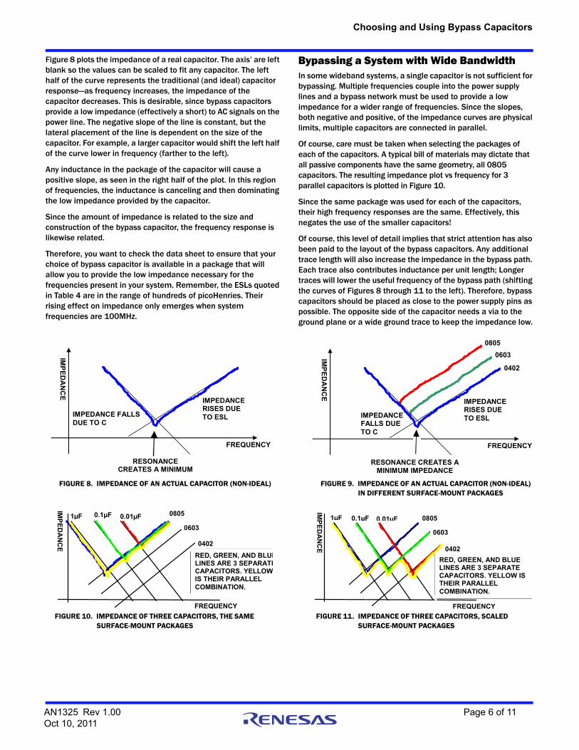
Figure 8 plots the impedance of a real capacitor. The axis’ are left blank so the values can be scaled to fit any capacitor. The left half of the curve represents the traditional (and ideal) capacitor response—as frequency increases, the impedance of the capacitor decreases. This is desirable, since bypass capacitors provide a low impedance (effectively a short) to AC signals on the power line. The negative slope of the line is constant, but the lateral placement of the line is dependent on the size of the capacitor. For example, a larger capacitor would shift the left half of the curve lower in frequency (farther to the left).
Any inductance in the package of the capacitor will cause a positive slope, as seen in the right half of the plot. In this region of frequencies, the inductance is canceling and then dominating the low impedance provided by the capacitor.
Since the amount of impedance is related to the size and construction of the bypass capacitor, the frequency response is likewise related.
Therefore, you want to check the data sheet to ensure that your choice of bypass capacitor is available in a package that will allow you to provide the low impedance necessary for the frequencies present in your system. Remember, the ESLs quoted in Table 4 are in the range of hundreds of picoHenries. Their rising effect on impedance only emerges when system frequencies are 100MHz.
Bypassing a System with Wide BandwidthIn some wideband systems, a single capacitor is not sufficient for bypassing. Multiple frequencies couple into the power supply lines and a bypass network must be used to provide a low impedance for a wider range of frequencies. Since the slopes, both negative and positive, of the impedance curves are physical limits, multiple capacitors are connected in parallel.
Of course, care must be taken when selecting the packages of each of the capacitors. A typical bill of materials may dictate that all passive components have the same geometry, all 0805 capacitors. The resulting impedance plot vs frequency for 3 parallel capacitors is plotted in Figure 10.
Since the same package was used for each of the capacitors, their high frequency responses are the same. Effectively, this negates the use of the smaller capacitors!
Of course, this level of detail implies that strict attention has also been paid to the layout of the bypass capacitors. Any additional trace length will also increase the impedance in the bypass path. Each trace also contributes inductance per unit length; Longer traces will lower the useful frequency of the bypass path (shifting the curves of Figures 8 through 11 to the left). Therefore, bypass capacitors should be placed as close to the power supply pins as possible. The opposite side of the capacitor needs a via to the ground plane or a wide ground trace to keep the impedance low.
FIGURE 8. IMPEDANCE OF AN ACTUAL CAPACITOR (NON-IDEAL) FIGURE 9. IMPEDANCE OF AN ACTUAL CAPACITOR (NON-IDEAL) IN DIFFERENT SURFACE-MOUNT PACKAGES
FIGURE 10. IMPEDANCE OF THREE CAPACITORS, THE SAME SURFACE-MOUNT PACKAGES
FIGURE 11. IMPEDANCE OF THREE CAPACITORS, SCALED SURFACE-MOUNT PACKAGES
IMPEDANCE RISES DUE TO ESL IMPEDANCE FALLS
DUE TO C
FREQUENCY
IMP
ED
AN
CE
RESONANCE CREATES A MINIMUM
IMPEDANCE RISES DUE TO ESL IMPEDANCE
FALLS DUE TO C
FREQUENCY
IMP
ED
AN
CE
RESONANCE CREATES A MINIMUM IMPEDANCE
0402
0603
0805
0805
0603
0402
0.01µF 0.1µF 1µF
FREQUENCY
IMP
ED
AN
CE
RED, GREEN, AND BLUELINES ARE 3 SEPARATECAPACITORS. YELLOWIS THEIR PARALLEL COMBINATION.
0805
0603
0402
0.01µF0.1µF 1µF
FREQUENCY
IMP
ED
AN
CE
RED, GREEN, AND BLUE LINES ARE 3 SEPARATE CAPACITORS. YELLOW IS THEIR PARALLEL COMBINATION.
AN1325 Rev 1.00 Page 6 of 11Oct 10, 2011
Choosing and Using Bypass Capacitors
Bypass Capacitor Application ExamplesSo far we have presented the main issues involved in designing optimum bypass networks. However, each circuit and each system will have specific demands that need to be addressed. The trade-offs involved in each particular instance can frustrate the best designers. Therefore, four different application examples are presented here. These examples have been chosen as representative of low current/low frequency, low current/high frequency, high current/low frequency and high current/high frequency systems. Table 5 shows the chosen circuits.
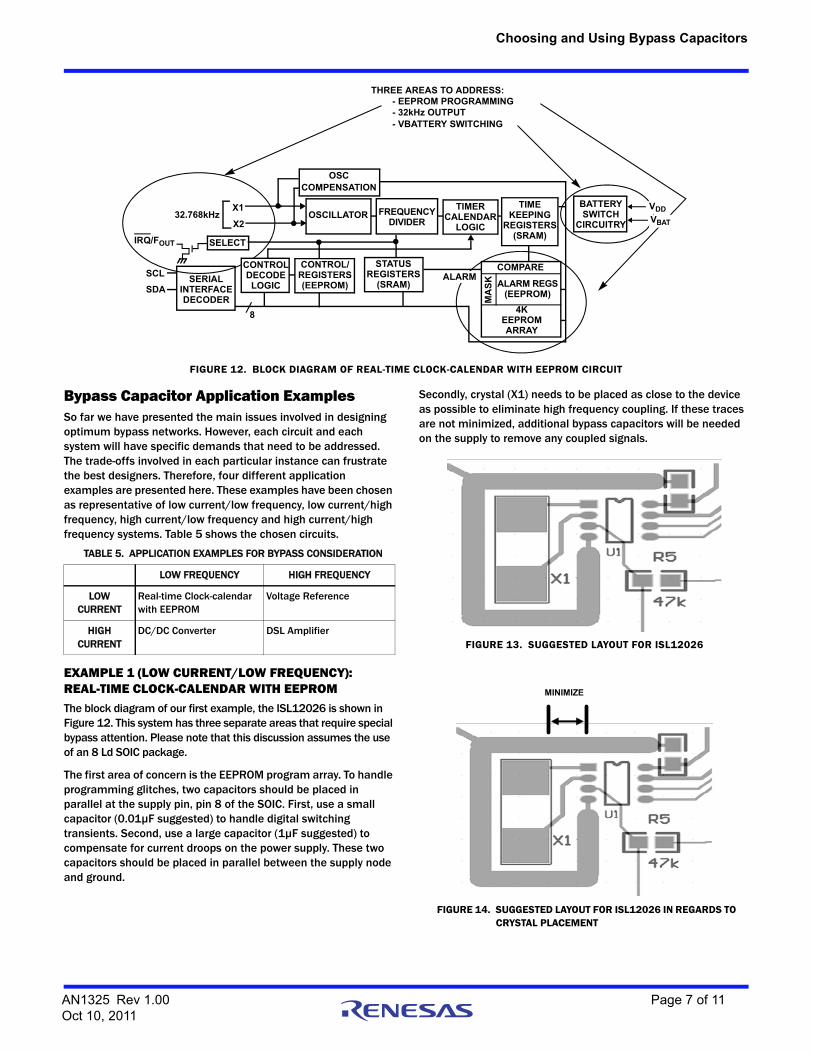
EXAMPLE 1 (LOW CURRENT/LOW FREQUENCY): REAL-TIME CLOCK-CALENDAR WITH EEPROMThe block diagram of our first example, the ISL12026 is shown in Figure 12. This system has three separate areas that require special bypass attention. Please note that this discussion assumes the use of an 8 Ld SOIC package.
The first area of concern is the EEPROM program array. To handle programming glitches, two capacitors should be placed in parallel at the supply pin, pin 8 of the SOIC. First, use a small capacitor (0.01µF suggested) to handle digital switching transients. Second, use a large capacitor (1µF suggested) to compensate for current droops on the power supply. These two capacitors should be placed in parallel between the supply node and ground.
Secondly, crystal (X1) needs to be placed as close to the device as possible to eliminate high frequency coupling. If these traces are not minimized, additional bypass capacitors will be needed on the supply to remove any coupled signals.
FIGURE 12. BLOCK DIAGRAM OF REAL-TIME CLOCK-CALENDAR WITH EEPROM CIRCUIT
OSCCOMPENSATION
OSCILLATORBATTERYSWITCH
CIRCUITRY
COMPARE
MA
SK ALARM REGS
(EEPROM)
4KEEPROMARRAY
STATUSREGISTERS
(SRAM)SERIAL
INTERFACEDECODER
SCL
SDA
32.768kHzX1
X2
SELECTIRQ/FOUT
8
THREE AREAS TO ADDRESS:- EEPROM PROGRAMMING- 32kHz OUTPUT- VBATTERY SWITCHING
FREQUENCYDIVIDER
TIMERCALENDAR
LOGIC
TIMEKEEPING
REGISTERS(SRAM)
CONTROL/REGISTERS(EEPROM)
CONTROLDECODELOGIC
ALARM
VDD
VBAT
TABLE 5. APPLICATION EXAMPLES FOR BYPASS CONSIDERATION
LOW FREQUENCY HIGH FREQUENCY
LOW CURRENT
Real-time Clock-calendar with EEPROM
Voltage Reference
HIGH CURRENT
DC/DC Converter DSL AmplifierFIGURE 13. SUGGESTED LAYOUT FOR ISL12026
FIGURE 14. SUGGESTED LAYOUT FOR ISL12026 IN REGARDS TO CRYSTAL PLACEMENT
MINIMIZE
AN1325 Rev 1.00 Page 7 of 11Oct 10, 2011

Choosing and Using Bypass Capacitors
This device allows for battery back-up. That feature is designed with a hand-off between line and battery power. Within this hand-off region, there is an overlap where both supplies are connected to the device. This supply overlap may cause switching transients. Adding a 0.1µF capacitor in parallel with the battery will minimize these transients.
EXAMPLE 2 (LOW CURRENT/HIGH FREQUENCY): VOLTAGE REFERENCEThe block diagram of our second example uses the ISL60002 to provide a voltage reference. Although voltage references are typically considered low frequency devices, they must be bypassed over the entire bandwidth of the system they are serving. Figure 15 shows the ISL60002 voltage reference regulating the supply of a high speed ADC.
In this example (Figure 15), the input to the voltage regulator is bypassed with the standard 2-capacitor fashion previously discussed in the “sizing” section. The output of the regulator is also bypassed to provide a low-impedance supply to the ADC.
If the ADC (or any other load) has a large input capacitance, you may need to add an R-C to absorb switching transients and reduce ringing (Figure 16).
EXAMPLE 3 (HIGH CURRENT/LOW FREQUENCY): DC/DC CONVERTERThe simplified block diagram of a DC/DC converter is shown in Figure 17. A pulse-width modulator controls switches to manipulate currents through large inductors to create the desired output voltage.
The DC/DC converter circuit can be further simplified when considering only one of the switching states (Figure 18).
Typically, a lot of attention is paid to choosing the inductor. The quality of the capacitor is often taken for granted. The circuit from Figure 18 is expanded to include the parasitics of the capacitor (Figure 19).
FIGURE 15. VOLTAGE REGULATOR AND ADC BLOCK DIAGRAM
0.001µF TO 0.01µF
SERIAL BUS
10µF 0.01µFVIN = +3.0V
REF IN
ENABLESCKSDAT
12-BIT TO 24-BITA/D CONVERTER
ISL60002
GND
VOUTVIN
FIGURE 16. VOLTAGE REGULATOR BYPASSING WITH LARGE CAPACITIVE LOAD
LOADCIN = 1000pF
0.001µF TO 0.01µF
VIN = +3.0V
10µF 0.01µF
10µF
2k
ISL60002
GND
VOUTVIN
FIGURE 17. SIMPLIFIED BLOCK DIAGRAM OF A DC/DC CONVERTER
P6µPPWM
AC/DCPOWERSUPPLY
AN1325 Rev 1.00 Page 8 of 11Oct 10, 2011
Choosing and Using Bypass Capacitors
The effect of these parasitics is more apparent because of the large current through them. A summary is provided in Equation 4:
The output voltage will exhibit a ripple proportional to the amount of parasitic resistance (ESR) and parasitic inductance (ESL) associated with the capacitor, Co. The information in Table 2 allows the designer to choose the best capacitor for the performance of their DC/DC converter.
Of course, this circuit also needs bypassing at both the input and output as in the voltage regulator example. Layout is critical and multiple devices are commonly crowded around both supply terminals.
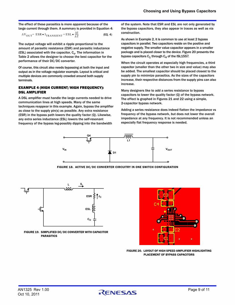
EXAMPLE 4 (HIGH CURRENT/HIGH FREQUENCY): DSL AMPLIFIERA DSL amplifier must handle the large currents needed to drive communication lines at high speeds. Many of the same techniques reappear in this example. Again, bypass the amplifier as close to the supply pin(s) as possible. Any extra resistance (ESR) in the bypass path lowers the quality factor (Q). Likewise, any extra series inductance (ESL) lowers the self-resonant frequency of the bypass leg-possibly dipping into the bandwidth
of the system. Note that ESR and ESL are not only generated by the bypass capacitors, they also appear in traces as well as via construction.
As shown in Example 2, it is common to use at least 2 bypass capacitors in parallel. Two capacitors reside on the positive and negative supply. The smaller value capacitor appears in a smaller package and is placed closer to the device. Figure 20 presents the bypass capacitors C1 through C4 of the ISL1557.
When the circuit operates at especially high frequencies, a third capacitor (smaller than the other two in size and value) may also be added. The smallest capacitor should be placed closest to the supply pin to minimize parasitics. As the sizes of the capacitors increase, their respective distances from the supply pins can also increase.
Many designers like to add a series resistance to bypass capacitors to lower the quality factor (Q) of the bypass network. The effect is graphed in Figures 21 and 22 using a simple, 2-capacitor bypass network.
Adding a series resistance does indeed flatten the impedance vs frequency of the bypass network, but does not lower the overall impedance at any frequency. It is not recommended unless an especially flat frequency response is needed.
VOUT ESR ITRANSIENT ESLIT-------+= (EQ. 4)
FIGURE 18. ACTIVE DC/DC CONVERTER CIRCUITRY IN ONE SWITCH CONFIGURATION
VOUTVIND1
L1
Q4
FIGURE 19. SIMPLIFIED DC/DC CONVERTER WITH CAPACITOR PARASITICS
ESR
ESL
CO
L IL
JC
FIGURE 20. LAYOUT OF HIGH SPEED AMPLIFIER HIGHLIGHTING PLACEMENT OF BYPASS CAPACITORS
AN1325 Rev 1.00 Page 9 of 11Oct 10, 2011

Choosing and Using Bypass Capacitors
SummaryAn introduction and overview of bypass capacitor and bypass techniques has been presented. Two main issues have been identified: high currents and high frequencies. Bypass capacitors must by chosen properly to handle the size and speed of transients. Parasitics need to be minimized. Many new specialized products are available for this very function (OSCON or X2Y). The most common solutions, however, use multi layer ceramic chips caps.
No matter which capacitor is chosen, layout is critical for quality bypassing. Bypass capacitors must be placed as close to the pins on the IC as possible to minimize additional ESR and ESL.
Finally, a number of applications examples are discussed. Their specifics provide insight into practical situations. One last resource is also provided (Table 6) which organizes other common circuits into our current/frequency matrix. Please use this guide to identify major issues and confidently design better bypass networks.
FIGURE 21. FREQUENCY RESPONSE OF TWO SCALED CAPACITORS IN PARALLEL (FOR REFERENCE)
C1 C2
FREQUENCY
IMP
ED
AN
CE
FIGURE 22. FREQUENCY RESPONSE OF TWO SCALED CAPACITORS IN PARALLEL. ONE CAPACITOR HAS BEEN DEQUED BY AN ADDITIONAL SERIES RESISTANCE
C1 C2
RSERIES
FREQUENCY
IMP
ED
AN
CE
TABLE 6. OTHER APPLICATION CIRCUITS WITH SIMILAR CURRENT AND FREQUENCY ISSUES
LOW FREQUENCY HIGH FREQUENCY
LOW CURRENT Precision AmpLight SensorsReal-time Clock/Calendar with EEPROM
High Speed AmplifierRF AmplifiersHigh Speed DAC/ADC
HIGH CURRENT Sample and HoldDC Restore AmplifierDC/DC Converter
Switching RegulatorRF AmplifiersPrecision DAC/ADCDSL Drivers/ReceiversHigh Speed Digital Clock
AN1325 Rev 1.00 Page 10 of 11Oct 10, 2011

http://www.renesas.comRefer to "http://www.renesas.com/" for the latest and detailed information.
Renesas Electronics America Inc.1001 Murphy Ranch Road, Milpitas, CA 95035, U.S.A.Tel: +1-408-432-8888, Fax: +1-408-434-5351Renesas Electronics Canada Limited9251 Yonge Street, Suite 8309 Richmond Hill, Ontario Canada L4C 9T3Tel: +1-905-237-2004Renesas Electronics Europe LimitedDukes Meadow, Millboard Road, Bourne End, Buckinghamshire, SL8 5FH, U.KTel: +44-1628-651-700, Fax: +44-1628-651-804Renesas Electronics Europe GmbHArcadiastrasse 10, 40472 Düsseldorf, Germany Tel: +49-211-6503-0, Fax: +49-211-6503-1327Renesas Electronics (China) Co., Ltd.Room 1709 Quantum Plaza, No.27 ZhichunLu, Haidian District, Beijing, 100191 P. R. ChinaTel: +86-10-8235-1155, Fax: +86-10-8235-7679Renesas Electronics (Shanghai) Co., Ltd.Unit 301, Tower A, Central Towers, 555 Langao Road, Putuo District, Shanghai, 200333 P. R. China Tel: +86-21-2226-0888, Fax: +86-21-2226-0999Renesas Electronics Hong Kong LimitedUnit 1601-1611, 16/F., Tower 2, Grand Century Place, 193 Prince Edward Road West, Mongkok, Kowloon, Hong KongTel: +852-2265-6688, Fax: +852 2886-9022Renesas Electronics Taiwan Co., Ltd.13F, No. 363, Fu Shing North Road, Taipei 10543, TaiwanTel: +886-2-8175-9600, Fax: +886 2-8175-9670Renesas Electronics Singapore Pte. Ltd.80 Bendemeer Road, Unit #06-02 Hyflux Innovation Centre, Singapore 339949Tel: +65-6213-0200, Fax: +65-6213-0300Renesas Electronics Malaysia Sdn.Bhd.Unit 1207, Block B, Menara Amcorp, Amcorp Trade Centre, No. 18, Jln Persiaran Barat, 46050 Petaling Jaya, Selangor Darul Ehsan, MalaysiaTel: +60-3-7955-9390, Fax: +60-3-7955-9510Renesas Electronics India Pvt. Ltd.No.777C, 100 Feet Road, HAL 2nd Stage, Indiranagar, Bangalore 560 038, IndiaTel: +91-80-67208700, Fax: +91-80-67208777Renesas Electronics Korea Co., Ltd.17F, KAMCO Yangjae Tower, 262, Gangnam-daero, Gangnam-gu, Seoul, 06265 KoreaTel: +82-2-558-3737, Fax: +82-2-558-5338
SALES OFFICES
© 2018 Renesas Electronics Corporation. All rights reserved.Colophon 7.0
(Rev.4.0-1 November 2017)
Notice
1. Descriptions of circuits, software and other related information in this document are provided only to illustrate the operation of semiconductor products and application examples. You are fully responsible for
the incorporation or any other use of the circuits, software, and information in the design of your product or system. Renesas Electronics disclaims any and all liability for any losses and damages incurred by
you or third parties arising from the use of these circuits, software, or information.
2. Renesas Electronics hereby expressly disclaims any warranties against and liability for infringement or any other claims involving patents, copyrights, or other intellectual property rights of third parties, by or
arising from the use of Renesas Electronics products or technical information described in this document, including but not limited to, the product data, drawings, charts, programs, algorithms, and application
examples.
3. No license, express, implied or otherwise, is granted hereby under any patents, copyrights or other intellectual property rights of Renesas Electronics or others.
4. You shall not alter, modify, copy, or reverse engineer any Renesas Electronics product, whether in whole or in part. Renesas Electronics disclaims any and all liability for any losses or damages incurred by
you or third parties arising from such alteration, modification, copying or reverse engineering.
5. Renesas Electronics products are classified according to the following two quality grades: “Standard” and “High Quality”. The intended applications for each Renesas Electronics product depends on the
product’s quality grade, as indicated below.
"Standard": Computers; office equipment; communications equipment; test and measurement equipment; audio and visual equipment; home electronic appliances; machine tools; personal electronic
equipment; industrial robots; etc.
"High Quality": Transportation equipment (automobiles, trains, ships, etc.); traffic control (traffic lights); large-scale communication equipment; key financial terminal systems; safety control equipment; etc.
Unless expressly designated as a high reliability product or a product for harsh environments in a Renesas Electronics data sheet or other Renesas Electronics document, Renesas Electronics products are
not intended or authorized for use in products or systems that may pose a direct threat to human life or bodily injury (artificial life support devices or systems; surgical implantations; etc.), or may cause
serious property damage (space system; undersea repeaters; nuclear power control systems; aircraft control systems; key plant systems; military equipment; etc.). Renesas Electronics disclaims any and all
liability for any damages or losses incurred by you or any third parties arising from the use of any Renesas Electronics product that is inconsistent with any Renesas Electronics data sheet, user’s manual or
other Renesas Electronics document.
6. When using Renesas Electronics products, refer to the latest product information (data sheets, user’s manuals, application notes, “General Notes for Handling and Using Semiconductor Devices” in the
reliability handbook, etc.), and ensure that usage conditions are within the ranges specified by Renesas Electronics with respect to maximum ratings, operating power supply voltage range, heat dissipation
characteristics, installation, etc. Renesas Electronics disclaims any and all liability for any malfunctions, failure or accident arising out of the use of Renesas Electronics products outside of such specified
ranges.
7. Although Renesas Electronics endeavors to improve the quality and reliability of Renesas Electronics products, semiconductor products have specific characteristics, such as the occurrence of failure at a
certain rate and malfunctions under certain use conditions. Unless designated as a high reliability product or a product for harsh environments in a Renesas Electronics data sheet or other Renesas
Electronics document, Renesas Electronics products are not subject to radiation resistance design. You are responsible for implementing safety measures to guard against the possibility of bodily injury, injury
or damage caused by fire, and/or danger to the public in the event of a failure or malfunction of Renesas Electronics products, such as safety design for hardware and software, including but not limited to
redundancy, fire control and malfunction prevention, appropriate treatment for aging degradation or any other appropriate measures. Because the evaluation of microcomputer software alone is very difficult
and impractical, you are responsible for evaluating the safety of the final products or systems manufactured by you.
8. Please contact a Renesas Electronics sales office for details as to environmental matters such as the environmental compatibility of each Renesas Electronics product. You are responsible for carefully and
sufficiently investigating applicable laws and regulations that regulate the inclusion or use of controlled substances, including without limitation, the EU RoHS Directive, and using Renesas Electronics
products in compliance with all these applicable laws and regulations. Renesas Electronics disclaims any and all liability for damages or losses occurring as a result of your noncompliance with applicable
laws and regulations.
9. Renesas Electronics products and technologies shall not be used for or incorporated into any products or systems whose manufacture, use, or sale is prohibited under any applicable domestic or foreign laws
or regulations. You shall comply with any applicable export control laws and regulations promulgated and administered by the governments of any countries asserting jurisdiction over the parties or
transactions.
10. It is the responsibility of the buyer or distributor of Renesas Electronics products, or any other party who distributes, disposes of, or otherwise sells or transfers the product to a third party, to notify such third
party in advance of the contents and conditions set forth in this document.
11. This document shall not be reprinted, reproduced or duplicated in any form, in whole or in part, without prior written consent of Renesas Electronics.
12. Please contact a Renesas Electronics sales office if you have any questions regarding the information contained in this document or Renesas Electronics products.
(Note 1) “Renesas Electronics” as used in this document means Renesas Electronics Corporation and also includes its directly or indirectly controlled subsidiaries.
(Note 2) “Renesas Electronics product(s)” means any product developed or manufactured by or for Renesas Electronics.