


Languages
Pages
Legal

ZXSC410/ZXSC420/ZXSC440 Document number: DS33618 Rev. 6 - 2
1 of 17 www.diodes.com
August 2015 © Diodes Incorporated
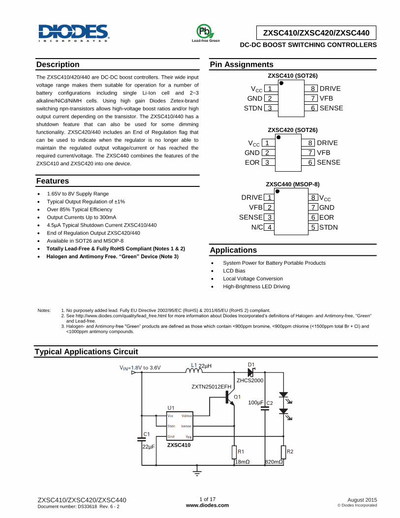
ZXSC410/ZXSC420/ZXSC440
DC-DC BOOST SWITCHING CONTROLLERS
Description
The ZXSC410/420/440 are DC-DC boost controllers. Their wide input
voltage range makes them suitable for operation for a number of
battery configurations including single Li-Ion cell and 2~3
alkaline/NiCd/NiMH cells. Using high gain Diodes Zetex-brand
switching npn-transistors allows high-voltage boost ratios and/or high
output current depending on the transistor. The ZXSC410/440 has a
shutdown feature that can also be used for some dimming
functionality. ZXSC420/440 includes an End of Regulation flag that
can be used to indicate when the regulator is no longer able to
maintain the regulated output voltage/current or has reached the
required current/voltage. The ZXSC440 combines the features of the
ZXSC410 and ZXSC420 into one device.
Features
1.65V to 8V Supply Range
Typical Output Regulation of ±1%
Over 85% Typical Efficiency
Output Currents Up to 300mA
4.5µA Typical Shutdown Current ZXSC410/440
End of Regulation Output ZXSC420/440
Available in SOT26 and MSOP-8
Totally Lead-Free & Fully RoHS Compliant (Notes 1 & 2)
Halogen and Antimony Free. “Green” Device (Note 3)
Pin Assignments
ZXSC410 (SOT26)
DRIVE
VFB
SENSE
VCC
GND
STDN
1
2
3
8
7
6
ZXSC420 (SOT26)
DRIVE
VFB
SENSE
VCC
GND
EOR
1
2
3
8
7
6
ZXSC440 (MSOP-8)
DRIVE
VFB
SENSE
N/C
VCC
GND
EOR
STDN
1
2
3
4
8
7
6
5
Applications
System Power for Battery Portable Products
LCD Bias
Local Voltage Conversion
High-Brightness LED Driving
Notes: 1. No purposely added lead. Fully EU Directive 2002/95/EC (RoHS) & 2011/65/EU (RoHS 2) compliant. 2. See http://www.diodes.com/quality/lead_free.html for more information about Diodes Incorporated’s definitions of Halogen- and Antimony-free, "Green" and Lead-free. 3. Halogen- and Antimony-free "Green” products are defined as those which contain <900ppm bromine, <900ppm chlorine (<1500ppm total Br + Cl) and <1000ppm antimony compounds.
Typical Applications Circuit
ZXSC410
ZXTN25012EFHZHCS2000
22µH
18mΩ 820mΩ
22µF
100µF

ZXSC410/ZXSC420/ZXSC440 Document number: DS33618 Rev. 6 - 2
2 of 17 www.diodes.com
August 2015 © Diodes Incorporated
ZXSC410/ZXSC420/ZXSC440
Pin Descriptions
Pin Name Pin Number
Function ZXSC410 ZXSC420 ZXSC440
VCC 1 1 8 Supply Voltage
GND 2 2 7 Ground
STDN 3 — 5 Shutdown (ZXSC410 and ZXSC440)
EOR — 3 6 End of regulation (ZXSC420 and ZXSC440)
Sense 4 4 3 Inductor current sense input. Internal threshold voltage set to 28mV.
Connect external sense resistor.
VFB 5 5 2 Reference voltage. Internal threshold set to 300mV.
Connect external resistor network to set output voltage.
Drive 6 6 1 Drive output for external switching transistor.
Connect to base or gate of external switching transistor.
NC — — 4 No connection
Functional Block Diagram
ZXSC410/ZXSC420/ZXSC440 Document number: DS33618 Rev. 6 - 2
3 of 17 www.diodes.com
August 2015 © Diodes Incorporated
ZXSC410/ZXSC420/ZXSC440
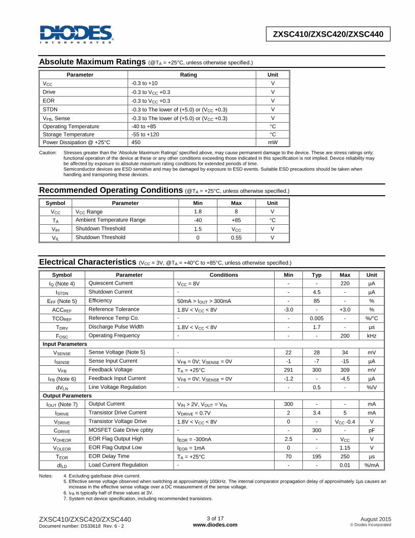
Absolute Maximum Ratings (@TA = +25°C, unless otherwise specified.)
Parameter Rating Unit
VCC -0.3 to +10 V
Drive -0.3 to VCC +0.3 V
EOR -0.3 to VCC +0.3 V
STDN -0.3 to The lower of (+5.0) or (VCC +0.3) V
VFB, Sense -0.3 to The lower of (+5.0) or (VCC +0.3) V
Operating Temperature -40 to +85 °C
Storage Temperature -55 to +120 °C
Power Dissipation @ +25°C 450 mW
Caution: Stresses greater than the 'Absolute Maximum Ratings' specified above, may cause permanent damage to the device. These are stress ratings only; functional operation of the device at these or any other conditions exceeding those indicated in this specification is not implied. Device reliability may be affected by exposure to absolute maximum rating conditions for extended periods of time. Semiconductor devices are ESD sensitive and may be damaged by exposure to ESD events. Suitable ESD precautions should be taken when handling and transporting these devices.
Recommended Operating Conditions (@TA = +25°C, unless otherwise specified.)
Symbol Parameter Min Max Unit
VCC VCC Range 1.8 8 V
TA Ambient Temperature Range -40 +85 °C
VIH Shutdown Threshold 1.5 VCC V
VIL Shutdown Threshold 0 0.55 V
Electrical Characteristics (VCC = 3V, @TA = +40°C to +85°C, unless otherwise specified.)
Symbol Parameter Conditions Min Typ Max Unit
IQ (Note 4) Quiescent Current VCC = 8V - - 220 µA
ISTDN Shutdown Current - - 4.5 - µA
EFF (Note 5) Efficiency 50mA > IOUT > 300mA - 85 - %
ACCREF Reference Tolerance 1.8V < VCC < 8V -3.0 - +3.0 %
TCOREF Reference Temp Co. - - 0.005 - %/°C
TDRV Discharge Pulse Width 1.8V < VCC < 8V - 1.7 - µs
FOSC Operating Frequency - - - 200 kHz
Input Parameters
VSENSE Sense Voltage (Note 5) - 22 28 34 mV
ISENSE Sense Input Current VFB = 0V; VSENSE = 0V -1 -7 -15 µA
VFB Feedback Voltage TA = +25°C 291 300 309 mV
IFB (Note 6) Feedback Input Current VFB = 0V; VSENSE = 0V -1.2 - -4.5 µA
dVLN Line Voltage Regulation - - 0.5 - %/V
Output Parameters
IOUT (Note 7) Output Current VIN > 2V, VOUT = VIN 300 - - mA
IDRIVE Transistor Drive Current VDRIVE = 0.7V 2 3.4 5 mA
VDRIVE Transistor Voltage Drive 1.8V < VCC < 8V 0 - VCC -0.4 V
CDRIVE MOSFET Gate Drive cpbty - - 300 - pF
VOHEOR EOR Flag Output High IEOR = -300nA 2.5 - VCC V
VOLEOR EOR Flag Output Low IEOR = 1mA 0 - 1.15 V
TEOR EOR Delay Time TA = +25°C 70 195 250 µs
dILD Load Current Regulation - - - 0.01 %/mA
Notes: 4. Excluding gate/base drive current. 5. Effective sense voltage observed when switching at approximately 100kHz. The internal comparator propagation delay of approximately 1µs causes an increase in the effective sense voltage over a DC measurement of the sense voltage.
6. IFB is typically half of these values at 3V.
7. System not device specification, including recommended transistors.
ZXSC410/ZXSC420/ZXSC440 Document number: DS33618 Rev. 6 - 2
4 of 17 www.diodes.com
August 2015 © Diodes Incorporated
ZXSC410/ZXSC420/ZXSC440
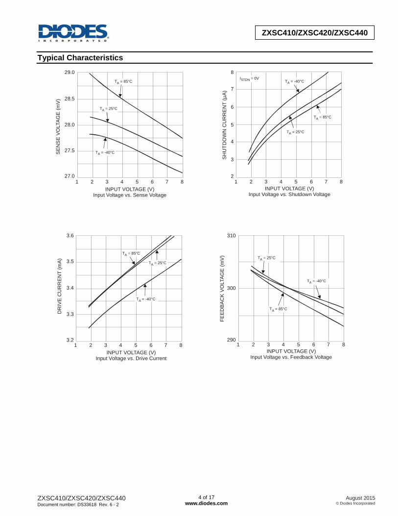
Typical Characteristics
1 82 3 4 5 6 7
29.0
27.0
28.5
28.0
27.5
INPUT VOLTAGE (V)Input Voltage vs. Sense Voltage
SE
NS
E V
OLTA
GE
(m
V)
T = -40°CA
T = 25°CA
T = 85°CA
1 82 3 4 5 6 7
8
7
3
2
6
5
4
INPUT VOLTAGE (V)Input Voltage vs. Shutdown Voltage
SH
UT
DO
WN
CU
RR
EN
T (
µA
)
T = -40°CA
T = 25°CA
T = 85°CA
I = 0VSTDN
1 82 3 4 5 6 7
3.5
3.2
3.4
3.3
3.6
INPUT VOLTAGE (V)Input Voltage vs. Drive Current
DR
IVE
CU
RR
EN
T (
mA
)
T = -40°CA
T = 25°CA
T = 85°CA
INPUT VOLTAGE (V)Input Voltage vs. Feedback Voltage
1 82 3 4 5 6 7
310
290
300
FE
ED
BA
CK
VO
LTA
GE
(m
V)
T = -40°CA
T = 25°CA
T = 85°CA

ZXSC410/ZXSC420/ZXSC440 Document number: DS33618 Rev. 6 - 2
5 of 17 www.diodes.com
August 2015 © Diodes Incorporated
ZXSC410/ZXSC420/ZXSC440
Application Information
Functional Blocks
Bandgap Reference
All threshold voltages and internal currents are derived from a temperature compensated bandgap reference circuit with a reference voltage of
1.22V nominal.
Dynamic Drive Output
Depending on the input signal, the output is either “LOW” or “HIGH”. In the high state a 2.5mA current source, (max drive voltage = VCC -0.4V)
drives the base or gate of the external transistor. In order to operate the external switching transistor at optimum efficiency, both output states
are initiated with a short transient current in order to quickly discharge the base or the gate of the switching transistor.
Switching Circuit
The switching circuit consists of two comparators, Comp1 and Comp2, a gate U1, a monostable and the drive output. Normally the DRIVE output
is “HIGH”; the external switching transistor is turned on. Current ramps up in the inductor, the switching transistor and external current sensing
resistor. This voltage is sensed by comparator, Comp2, at input ISENSE. Once the current sense voltage across the sensing resistor exceeds
20mV, comparator Comp2 through gate U1 triggers a re-triggerable monostable and turns off the output drive stage for 2μs. The inductor
discharges to the load of the application. After 2μs a new charge cycle begins, thus ramping the output voltage. When the output voltage reaches
the nominal value and VFB gets an input voltage of more than 300mV, the monostable is forced “on” from Comp1 through gate U1, until the
feedback voltage falls below 300mV. The above action continues to maintain regulation.
EOR, End of Regulation Detector (ZXSC420/440)
The EOR circuit is a retriggerable 120μs monostable, which is re-triggered by every down regulating action of comparator Comp1. As long as
regulation takes place, output EOR is “HIGH” (high impedance, 100K to VCC). Short dips of the output voltage of less than 120μs are ignored. If
the output voltage falls below the nominal value for more than 120μs, output EOR goes ”LOW”. The reason for this to happen is usually a slowly
progressing drop of input voltage from the discharging battery. Therefore, the output voltage will also start to drop slowly. With the EOR detector,
batteries can be used to the ultimate end of discharge, with enough time left for a safe shutdown. It can also be used in high-voltage photoflash
with the ZXSC440 to show when the capacitor is fully charged.
Shutdown Control
The ZXSC410/440 offers a shutdown mode that consumes a standby current of less than 5µA. The ZXSC410/440 is enabled, and is in normal
operation, when the voltage at the STDN pin is between 1V and 8V (and also open circuit). The ZXSC410/440 is shutdown with the driver
disabled when the voltage at the STDN pin is 0.7V or lower. The STDN input is a high impedance current source of 1µA typ. The driving device
can be an open-collector or -drain or a logic output with a “High” voltage of 5V max. The device shutdown current depends on the supply voltage,
(see typical characteristics graph).The ZXSC440 with its STDN pin and EOR pins can be used as a camera flash driver.
The STDN pin is used to initiate the high-voltage capacitor charge cycle. The EOR pin is used as flag to show when the capacitor has been
charged to the appropriate level.
A transformer is used to boost the voltage. If designing a transformer, bear in mind that the primary current may be over an amp and, if this flows
through 10 turns, the primary flux will be 10 Amp. Small number of turns and small cores will need an air gap to cope with this value without
saturation. Secondary winding capacitance should not be too high as this is working at 300V and could soon cause excessive losses.
ZXSC410/ZXSC420/ZXSC440 Document number: DS33618 Rev. 6 - 2
6 of 17 www.diodes.com
August 2015 © Diodes Incorporated
ZXSC410/ZXSC420/ZXSC440
Application Information (continued)
External Component Selection
Switching Transistor Selection
The choice of switching transistor has a major impact on the converter efficiency. For optimum performance, a bipolar transistor with low VCE(SAT)
and high gain is required. The VCEO of the switching transistor is also an important parameter as this sees the full output voltage when the
transistor is switched off. Diodes SOT26 transistors are an ideal choice for this application.
Schottky Diode Selection
As with the switching transistor, the Schottky rectifier diode has a major impact on the converter efficiency. A Schottky diode with a low forward
voltage and fast recovery time should be used for this application.
The diode should be selected so that the maximum forward current rating is greater or equal to the maximum peak current in the inductor, and
the maximum reverse voltage is greater or equal to the output voltage. The Diodes ZHCS Series meets these needs.
Inductor Selection
The inductor value must be chosen to satisfy performance, cost and size requirements of the overall solution.
Inductor selection has a significant impact on the converter performance. For applications where efficiency is critical, an inductor with a series
resistance of 500mΩ or less should be used.
Output Capacitors
Output capacitors are a critical choice in the overall performance of the solution. They are required to filter the output and supply load transient
currents. There are three parameters which are paramount in the selection of the output capacitors, capacitance, IRIPPLE and ESR. The
capacitance value is selected to meet the load transient requirements. The capacitors IRIPPLE rating must meet or exceed the current ripple of the
solution.
The ESR of the output capacitor can also affect loop stability and transient performance. The capacitors selected for the solutions and indicated
in the reference designs are optimized to provide the best overall performance.
Input Capacitors
The input capacitor is chosen for its voltage and RMS current rating. The use of low ESR electrolytic or tantalum capacitors is recommended.
Capacitor values for optimum performance are suggested in the reference design section.
Also note that the ESR of the input capacitor is effectively in series with the input and hence contributes to efficiency losses in the order of IRMS2
ESR.
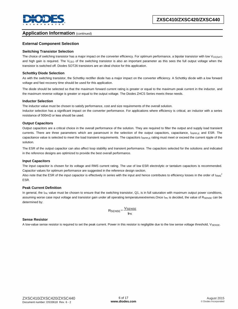
Peak Current Definition
In general, the IPK value must be chosen to ensure that the switching transistor, Q1, is in full saturation with maximum output power conditions,
assuming worse case input voltage and transistor gain under all operating temperatureextremes.Once IPK is decided, the value of RSENSE can be
determined by:
I
VR
PK
SENSESENSE
Sense Resistor
A low-value sense resistor is required to set the peak current. Power in this resistor is negligible due to the low sense voltage threshold, VSENSE.
ZXSC410/ZXSC420/ZXSC440 Document number: DS33618 Rev. 6 - 2
7 of 17 www.diodes.com
August 2015 © Diodes Incorporated
ZXSC410/ZXSC420/ZXSC440
Application Information (cont.)
Output Power Calculation
By making the above assumptions for inductance and peak current the output power can be determined by:
POUT = IAV x VIN x η = (Watts) Where:
tt
ttx
2
II
OFFON
DISONPKAV
and,
V
L It
IN
PKON
and,
VV
L It
INOUT
PKDIS
and,
tOFF ≈ 1.7μs (internally set by ZXSC410/420/440)
and,
η = efficiency i.e. 100% = 1
Operating frequency can be derived by:
tt
1f
OFFON
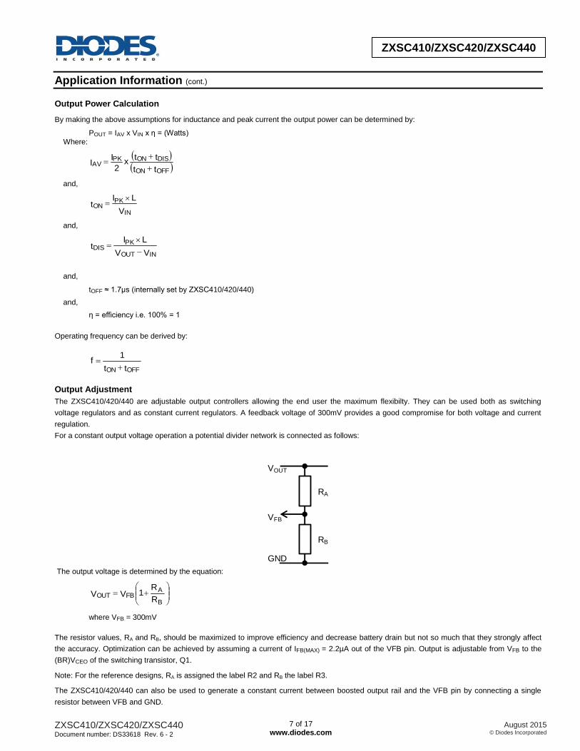
Output Adjustment
The ZXSC410/420/440 are adjustable output controllers allowing the end user the maximum flexibilty. They can be used both as switching
voltage regulators and as constant current regulators. A feedback voltage of 300mV provides a good compromise for both voltage and current
regulation.
For a constant output voltage operation a potential divider network is connected as follows:
VFB
VOUT
GND
RA
RB
The output voltage is determined by the equation:
B
AFBOUT
R
R1VV
where VFB = 300mV
The resistor values, RA and RB, should be maximized to improve efficiency and decrease battery drain but not so much that they strongly affect
the accuracy. Optimization can be achieved by assuming a current of IFB(MAX) = 2.2µA out of the VFB pin. Output is adjustable from VFB to the
(BR)VCEO of the switching transistor, Q1.
Note: For the reference designs, RA is assigned the label R2 and RB the label R3.
The ZXSC410/420/440 can also be used to generate a constant current between boosted output rail and the VFB pin by connecting a single
resistor between VFB and GND.
ZXSC410/ZXSC420/ZXSC440 Document number: DS33618 Rev. 6 - 2
8 of 17 www.diodes.com
August 2015 © Diodes Incorporated
ZXSC410/ZXSC420/ZXSC440
Application Information (cont.)
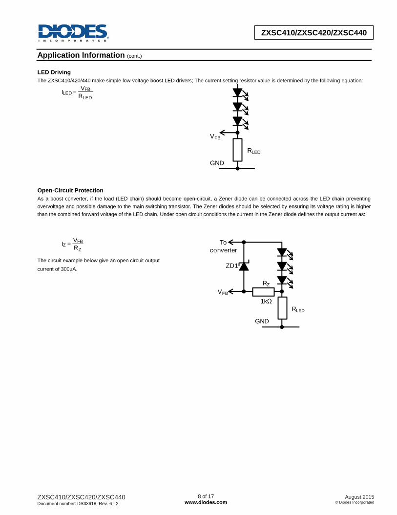
LED Driving
The ZXSC410/420/440 make simple low-voltage boost LED drivers; The current setting resistor value is determined by the following equation:
LED
FBLED
R
VI
VFB
GND
RLED
Open-Circuit Protection
As a boost converter, if the load (LED chain) should become open-circuit, a Zener diode can be connected across the LED chain preventing
overvoltage and possible damage to the main switching transistor. The Zener diodes should be selected by ensuring its voltage rating is higher
than the combined forward voltage of the LED chain. Under open circuit conditions the current in the Zener diode defines the output current as:
Z
FBZ
R
VI
The circuit example below give an open circuit output
current of 300µA.
VFB
GND
RLED
RZ
1kΩ
ZD1
To
converter

ZXSC410/ZXSC420/ZXSC440 Document number: DS33618 Rev. 6 - 2
9 of 17 www.diodes.com
August 2015 © Diodes Incorporated
ZXSC410/ZXSC420/ZXSC440
Application Information (cont.)
Dimming Control There are many types of dimming control that can be implemented for the ZXSC410/420/440.
Dimming Control Using the Shutdown Pin
The first method uses the shutdown pin (only ZXSC410 and
ZXSC440). By injecting a PWM waveform on this pin and varying the
duty cycle, LED current and hence LED brightness can be adjusted.
To implement this method of brightness control on the ZXSC410/440,
a PWM signal with an amplitude between 0.7V and VCC at a
frequency of 120Hz or above (to eliminate LED flicker) should be
applied to the STDN pin. The LED current and hence LED brightness
is linearly proportional to the duty cycle ratio, so for brightness control
adjust the duty cycle ratio as necessary. For example, a 10% duty
cycle equates to 10% of full LED brightness.
30
0
10
OU
TP
UT
CU
RR
EN
T (
A)
20
40 20 0100 80 60
DUTY CYCLE (%)LED Current vs. Duty Cycle
4 White LEDsV = V = 3.3VIN EN
Dimming Control Using a DC Voltage
For applications where a PWM signal is not available or for the ZXSC420 a DC voltage can be used to control dimming by modulating the VFB pin.
By adding resistors R2 and R3 and applying a DC voltage, the LED
current can be adjusted from 100% to 0%. As the DC voltage
increases, the voltage drop across R2 increases and the voltage drop
across R1 decreases, thus reducing the current through the LEDs.
Selection of R2 and R3 should ensure that the current from the DC
voltage is much less than the LED current and much larger than the
feedback current. The component values in the diagram above
represent 0% to 100% dimming control from a 0 to 2V DC voltage.
R2
10k
R3
67kR1
VFB
VDC
Dimming Control Using a Filtered PWM Signal
The filtered PWM signal can be considered as an adjustable
DC voltage by applying a RC filter (R4 and C1). The values
shown in the diagram below are configured to give 0% to
100% dimming for a 1kHz to 100kHz PWM signal with a 2V
amplitude. e.g. a 50% duty cycle will give 50% dimming.
C1
0.1µF
R2
10k
R3
67kR1
VFB
PWM
R4
10k

ZXSC410/ZXSC420/ZXSC440 Document number: DS33618 Rev. 6 - 2
10 of 17 www.diodes.com
August 2015 © Diodes Incorporated
ZXSC410/ZXSC420/ZXSC440
Application Information (cont.)
Dimming Control using a Logic Signal
For applications where the LED current needs to be adjusted in
discrete steps a logic signal can be applied as shown in the diagram
below.
When Q1 is ‘off’, R1 sets the minimum LED current. When Q1 is ‘on’,
R2 sets the LED current that will be added to the minimum LED
current. The formula for selecting values for R1 and R2 are given
below:
MOSFET ‘off’
1
FB)MIN(LED
R
VI I
R2
R1
VFB
LOGIC
SIGNAL
Q1
2N7002
MOSFET ‘on’
)MIN(LED2
FB)MAX(LED I
R
VI
Layout Issues
Layout is critical for the circuit to function in the most efficient manner in terms of electrical efficiency, thermal considerations and noise.
For ‘step-up converters’ there are four main current loops, the input loop, power-switch loop, rectifier loop and output loop. The supply charging
the input capacitor forms the input loop. The power-switch loop is defined when Q1 is ‘on’, current flows from the input through the inductor, Q1,
RSENSE and to ground. When Q1 is ‘off’, the energy stored in the inductor is transferred to the output capacitor and load via D1, forming the
rectifier loop. The output loop is formed by the output capacitor supplying the load when Q1 is switched back off.
To optimize for best performance, each of these loops is kept separate from one another and interconnected with short, thick traces, thus
minimizing parasitic inductance, capacitance and resistance. Also the RSENSE resistor should be connected with minimum trace length, between
emitter lead of Q1 and ground, (again minimizing stray parasitics).
ZXSC410/ZXSC420/ZXSC440 Document number: DS33618 Rev. 6 - 2
11 of 17 www.diodes.com
August 2015 © Diodes Incorporated
ZXSC410/ZXSC420/ZXSC440
Application Examples
ZXSC410 DC-DC Boost Voltage Regulators
VIN = 2.5V to 4.2V, VOUT = 5V; ILOAD = 100mA
0 20 40 60 80 100
100
70
90
80EF
FIC
IEN
CY
(%
)
LOAD CURRENT (mA)Load Current vs. Efficiency
V = 3.6VINV = 4.2VIN
V = 3VIN
2.5 3.0 3.5 4.0
100
70
90
80EF
FIC
IEN
CY
(%
)
INPUT VOLTAGE (V)Input Voltage vs. Efficiency
I = 10mALOAD
I = 100mALOAD
I = 60mALOAD
Switching Waveform
Output Ripple
ZXSC410
ZXTN25012EFH ZHCS2000
22µH
100m Ω 1k Ω
22µF
22µF
V IN = 2.5V to 4.2V
R3 16k Ω
C3 100nF
ZXSC410/ZXSC420/ZXSC440 Document number: DS33618 Rev. 6 - 2
12 of 17 www.diodes.com
August 2015 © Diodes Incorporated
ZXSC410/ZXSC420/ZXSC440
Application Examples (continued)
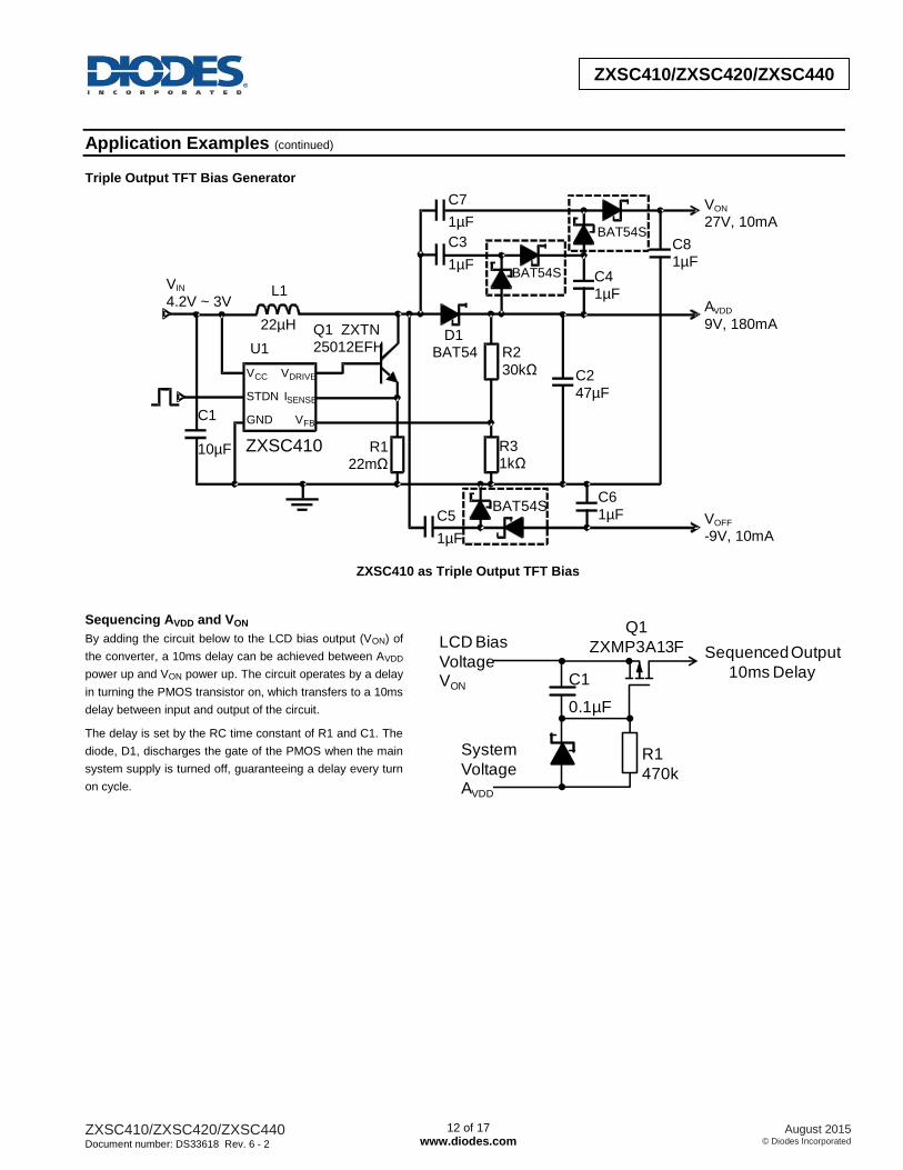
Triple Output TFT Bias Generator
ZXSC410 as Triple Output TFT Bias
Sequencing AVDD and VON
By adding the circuit below to the LCD bias output (VON) of
the converter, a 10ms delay can be achieved between AVDD
power up and VON power up. The circuit operates by a delay
in turning the PMOS transistor on, which transfers to a 10ms
delay between input and output of the circuit.
The delay is set by the RC time constant of R1 and C1. The
diode, D1, discharges the gate of the PMOS when the main
system supply is turned off, guaranteeing a delay every turn
on cycle.
System
VoltageAVDD
C1
0.1µF
R1
470k
LCD Bias
VoltageVON
Q1
ZXMP3A13F Sequenced Output
10ms Delay
ZXSC410
Q1 ZXTN 25012EFH
C1
10µF
C5
1µF
C2 47µF
R1 22m Ω
R2 30k Ω
R3 1k Ω
L1
22µH
U1 D1
BAT54 V CC
STDN
GND
V DRIVE
I SENSE
V FB
C7
1µF
C6 1µF
C8 1µF
C4 1µF
V ON 27V, 10mA
A VDD 9V, 180mA
V OFF - 9V, 10mA
C3
1µF V IN 4.2V ~ 3V
BAT54S
BAT54S
BAT54S
ZXSC410/ZXSC420/ZXSC440 Document number: DS33618 Rev. 6 - 2
13 of 17 www.diodes.com
August 2015 © Diodes Incorporated
ZXSC410/ZXSC420/ZXSC440
Application Examples (cont.)
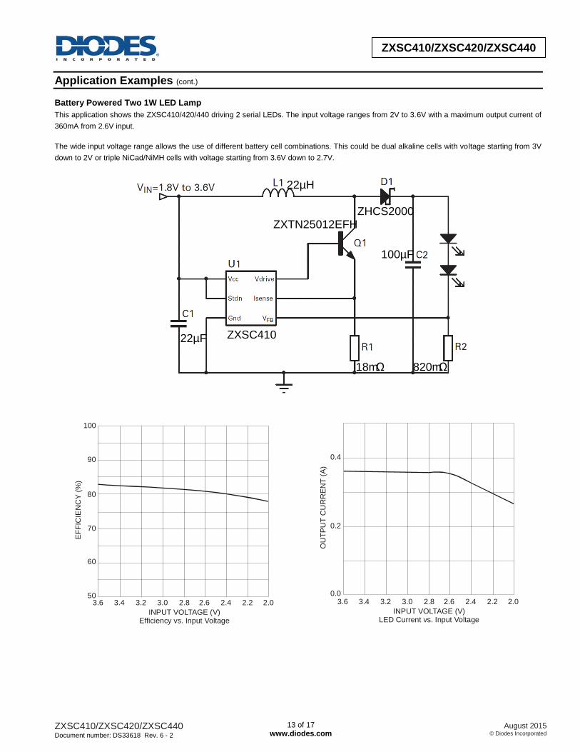
Battery Powered Two 1W LED Lamp
This application shows the ZXSC410/420/440 driving 2 serial LEDs. The input voltage ranges from 2V to 3.6V with a maximum output current of
360mA from 2.6V input.
The wide input voltage range allows the use of different battery cell combinations. This could be dual alkaline cells with voltage starting from 3V
down to 2V or triple NiCad/NiMH cells with voltage starting from 3.6V down to 2.7V.
2.8 2.6 2.4 2.2 2.03.6 3.4 3.2 3.0
INPUT VOLTAGE (V)Efficiency vs. Input Voltage
100
90
60
50
80
70
EF
FIC
IEN
CY
(%
)
0.4
0.0
0.2
OU
TP
UT
CU
RR
EN
T (
A)
2.8 2.6 2.4 2.2 2.03.6 3.4 3.2 3.0
INPUT VOLTAGE (V)LED Current vs. Input Voltage
ZXSC410
ZXTN25012EFH
ZHCS2000
22µH
18m Ω 820m Ω
22µF
100µF
ZXSC410/ZXSC420/ZXSC440 Document number: DS33618 Rev. 6 - 2
14 of 17 www.diodes.com
August 2015 © Diodes Incorporated
ZXSC410/ZXSC420/ZXSC440
Application Examples (cont.)
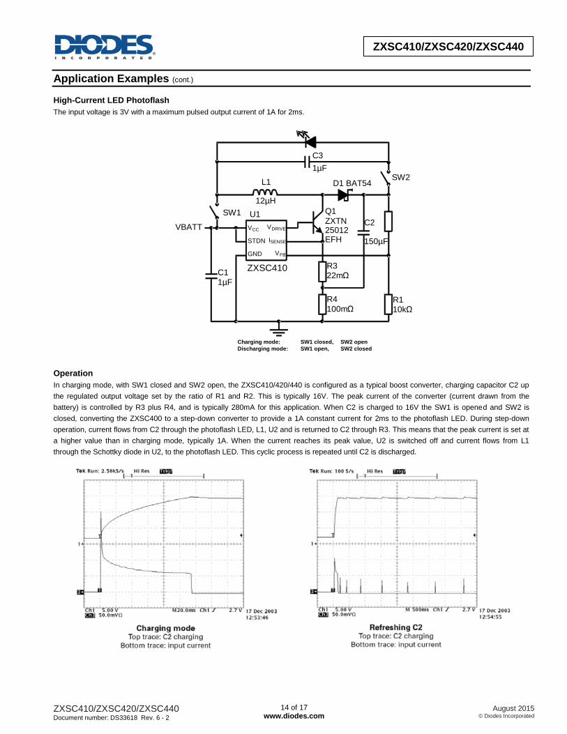
High-Current LED Photoflash
The input voltage is 3V with a maximum pulsed output current of 1A for 2ms.
Operation
In charging mode, with SW1 closed and SW2 open, the ZXSC410/420/440 is configured as a typical boost converter, charging capacitor C2 up
the regulated output voltage set by the ratio of R1 and R2. This is typically 16V. The peak current of the converter (current drawn from the
battery) is controlled by R3 plus R4, and is typically 280mA for this application. When C2 is charged to 16V the SW1 is opened and SW2 is
closed, converting the ZXSC400 to a step-down converter to provide a 1A constant current for 2ms to the photoflash LED. During step-down
operation, current flows from C2 through the photoflash LED, L1, U2 and is returned to C2 through R3. This means that the peak current is set at
a higher value than in charging mode, typically 1A. When the current reaches its peak value, U2 is switched off and current flows from L1
through the Schottky diode in U2, to the photoflash LED. This cyclic process is repeated until C2 is discharged.
ZXSC410
Q1 ZXTN 25012 EFH
C1 1µF
C3 1µF
C2
150µF
R3 22m Ω
R4 100m Ω
R1 10k Ω
L1
12µH
U1 SW1
SW2
VBATT
D1 BAT54
V CC STDN
GND
V DRIVE I SENSE
V FB
Charging mode: SW1 closed, SW2 open Discharging mode: SW1 open, SW2 closed
ZXSC410/ZXSC420/ZXSC440 Document number: DS33618 Rev. 6 - 2
15 of 17 www.diodes.com
August 2015 © Diodes Incorporated
ZXSC410/ZXSC420/ZXSC440
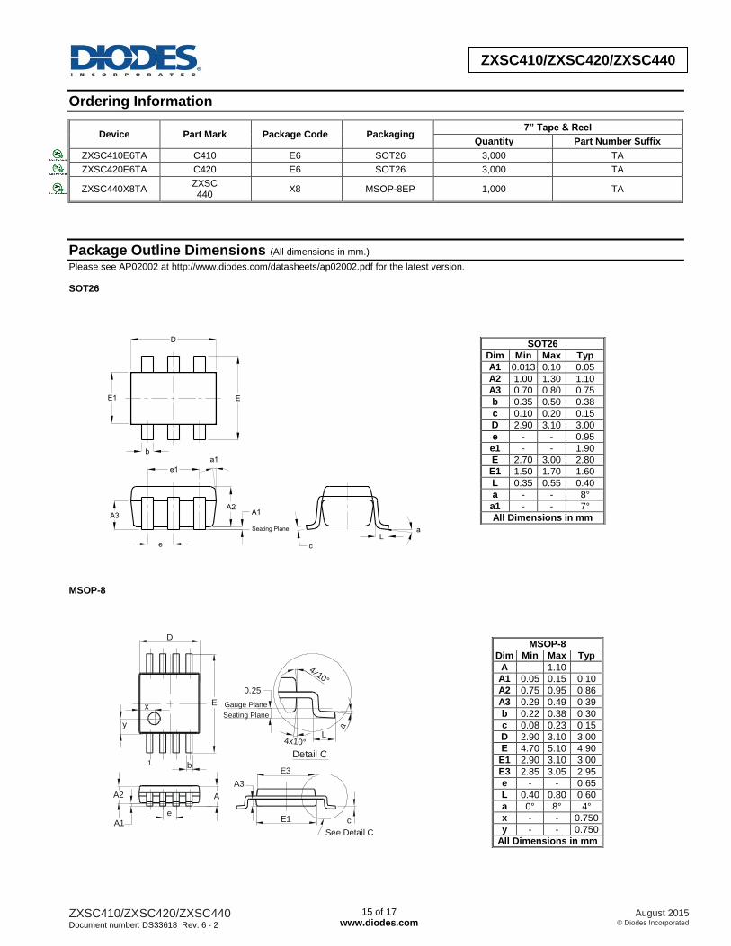
Ordering Information
Device Part Mark Package Code Packaging 7” Tape & Reel
Quantity Part Number Suffix
ZXSC410E6TA C410 E6 SOT26 3,000 TA
ZXSC420E6TA C420 E6 SOT26 3,000 TA
ZXSC440X8TA ZXSC 440
X8 MSOP-8EP 1,000 TA
Package Outline Dimensions (All dimensions in mm.)
Please see AP02002 at http://www.diodes.com/datasheets/ap02002.pdf for the latest version.
SOT26
a1
D
e
E1 E
b
A2A1
Seating Plane
L
c
a
e1
A3
MSOP-8
SOT26
Dim Min Max Typ
A1 0.013 0.10 0.05
A2 1.00 1.30 1.10
A3 0.70 0.80 0.75
b 0.35 0.50 0.38
c 0.10 0.20 0.15
D 2.90 3.10 3.00
e - - 0.95
e1 - - 1.90
E 2.70 3.00 2.80
E1 1.50 1.70 1.60
L 0.35 0.55 0.40
a - - 8°
a1 - - 7°
All Dimensions in mm
MSOP-8
Dim Min Max Typ
A - 1.10 -
A1 0.05 0.15 0.10
A2 0.75 0.95 0.86
A3 0.29 0.49 0.39
b 0.22 0.38 0.30
c 0.08 0.23 0.15
D 2.90 3.10 3.00
E 4.70 5.10 4.90
E1 2.90 3.10 3.00
E3 2.85 3.05 2.95
e - - 0.65
L 0.40 0.80 0.60
a 0° 8° 4°
x - - 0.750
y - - 0.750
All Dimensions in mm
A
A1
A2
e
Seating Plane
Gauge Plane
L
See Detail C
Detail C
c
a
E1
E3
A3
1
E
y
x
D
b
0.25
4x10°
4x10°

ZXSC410/ZXSC420/ZXSC440 Document number: DS33618 Rev. 6 - 2
16 of 17 www.diodes.com
August 2015 © Diodes Incorporated
ZXSC410/ZXSC420/ZXSC440
Suggested Pad Layout Please see AP02001 at http://www.diodes.com/datasheets/ap02001.pdf for the latest version. SOT26
C1
Y1 G
X
Y
C
MSOP-8
Dimensions Value (in mm)
C 2.40
C1 0.95
G 1.60
X 0.55
Y 0.80
Y1 3.20
Dimensions Value (in mm)
C 0.650
X 0.450
Y 1.350
Y1 5.300
X C
Y
Y1

ZXSC410/ZXSC420/ZXSC440 Document number: DS33618 Rev. 6 - 2
17 of 17 www.diodes.com
August 2015 © Diodes Incorporated
ZXSC410/ZXSC420/ZXSC440
IMPORTANT NOTICE DIODES INCORPORATED MAKES NO WARRANTY OF ANY KIND, EXPRESS OR IMPLIED, WITH REGARDS TO THIS DOCUMENT, INCLUDING, BUT NOT LIMITED TO, THE IMPLIED WARRANTIES OF MERCHANTABILITY AND FITNESS FOR A PARTICULAR PURPOSE (AND THEIR EQUIVALENTS UNDER THE LAWS OF ANY JURISDICTION). Diodes Incorporated and its subsidiaries reserve the right to make modifications, enhancements, improvements, corrections or other changes without further notice to this document and any product described herein. Diodes Incorporated does not assume any liability arising out of the application or use of this document or any product described herein; neither does Diodes Incorporated convey any license under its patent or trademark rights, nor the rights of others. Any Customer or user of this document or products described herein in such applications shall assume all risks of such use and will agree to hold Diodes Incorporated and all the companies whose products are represented on Diodes Incorporated website, harmless against all damages. Diodes Incorporated does not warrant or accept any liability whatsoever in respect of any products purchased through unauthorized sales channel. Should Customers purchase or use Diodes Incorporated products for any unintended or unauthorized application, Customers shall indemnify and hold Diodes Incorporated and its representatives harmless against all claims, damages, expenses, and attorney fees arising out of, directly or indirectly, any claim of personal injury or death associated with such unintended or unauthorized application. Products described herein may be covered by one or more United States, international or foreign patents pending. Product names and markings noted herein may also be covered by one or more United States, international or foreign trademarks. This document is written in English but may be translated into multiple languages for reference. Only the English version of this document is the final and determinative format released by Diodes Incorporated.
LIFE SUPPORT Diodes Incorporated products are specifically not authorized for use as critical components in life support devices or systems without the express written approval of the Chief Executive Officer of Diodes Incorporated. As used herein: A. Life support devices or systems are devices or systems which: 1. are intended to implant into the body, or
2. support or sustain life and whose failure to perform when properly used in accordance with instructions for use provided in the labeling can be reasonably expected to result in significant injury to the user.
B. A critical component is any component in a life support device or system whose failure to perform can be reasonably expected to cause the failure of the life support device or to affect its safety or effectiveness. Customers represent that they have all necessary expertise in the safety and regulatory ramifications of their life support devices or systems, and acknowledge and agree that they are solely responsible for all legal, regulatory and safety-related requirements concerning their products and any use of Diodes Incorporated products in such safety-critical, life support devices or systems, notwithstanding any devices- or systems-related information or support that may be provided by Diodes Incorporated. Further, Customers must fully indemnify Diodes Incorporated and its representatives against any damages arising out of the use of Diodes Incorporated products in such safety-critical, life support devices or systems. Copyright © 2015, Diodes Incorporated www.diodes.com
Top Related