


Languages
Pages
Legal

© 2016 LitePoint, A Teradyne Company. All rights reserved.
TECHNICAL SPECIFICATIONS
z8451Signal AnalyzerPXI, PXIe
Signal Analyzer 2
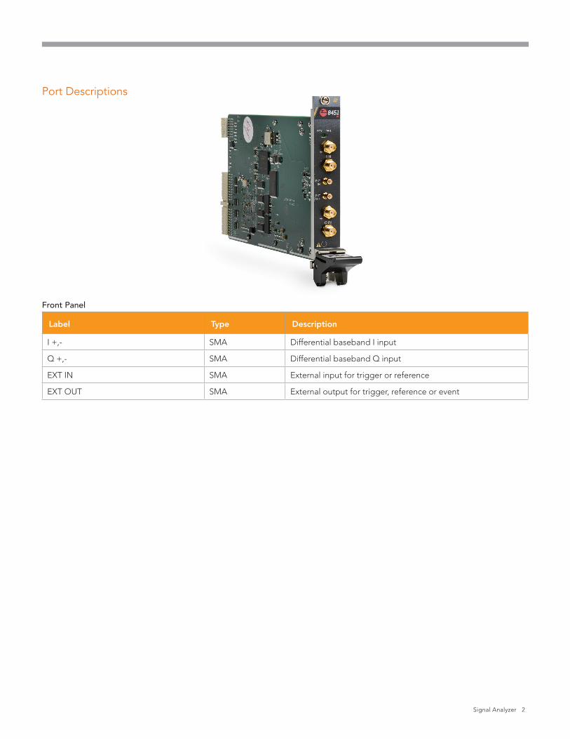
Port Descriptions
Front Panel
Label Type Description
I +,- SMA Differential baseband I input
Q +,- SMA Differential baseband Q input
EXT IN SMA External input for trigger or reference
EXT OUT SMA External output for trigger, reference or event
Signal Analyzer 3
Inputs
I/Q Input Channels
Specification Value
Channels Two Differential Input Channels, I+/- and Q+/- (One I/Q)
Input ImpedanceSingle-endedDifferential
50 Ω100 Ω≤ ±1% accuracy
Input VSWRDC to 250 MHz
≤ 1.3:1
Input Bias Current ≤ ±10 μA
Connectors SMA
I/Q Input Voltage
Specification Value
Absolute Maximum Input (no damage)Single-ended -2 V to +5 V (DC + peak AC), CAT I
Input Voltage Ranges
+10 dBm ( 2 Vppd)0 dBm ( 0.63 Vppd)-10 dBm ( 0.2 Vppd)-20 dBm ( 0.063 Vppd)
Input Voltage Range Accuracy (1 MHz)≤ ±0.05 dB at 25°C ambient≤ ±0.01 dB drift per °C
Input Offset Adjustment±1 V4 μV resolution
Input Offset Accuracy< ±(2 mV + 0.5% offset) at 25°C≤ ±200 μV drift per °C
Signal Analyzer 4
I/Q Input Dynamic Performance
Specification Value
Analog Bandwidth -3 dB BandwidthStopband Rejection
DC to 300 MHz≥80 dB at 800 MHz
Spurious-Free Dynamic Range (excluding harmonics)
≥ 80 dBc at 10 MHz
Harmonic Distortion ≥ 75 dBc at 10 MHz
Intermodulation Distortion (2 tone, 10.6 MHz & 10.8 MHz)
≥ 80 dBc
Average Noise Density+10 dBm Range0 dBm Range-10 dBm Range-20 dBm Range
≤ -145 dBm/Hz (-155 dBFS/Hz)≤ -150 dBm/Hz (-150 dBFS/Hz)≤ -153 dBm/Hz (-143 dBFS/Hz)≤ -154 dBm/Hz (-134 dBFS/Hz)
Phase Noise (187.5 MHz, typical)1 kHz offset frequency10 kHz offset frequency100 kHz offset frequency1 MHz offset frequency10 MHz offset frequency
-110 dBc/Hz-130 dBc/Hz-132 dBc/Hz-138 dBc/Hz-140 dBc/Hz
I/Q Channel-to-Channel Match (DC to 50 MHz, same range settings)
≤ 0.2 dB magnitude≤ 0.5° phase
I/Q Channel-to-Channel IsolationDC to 100 MHz100 MHz to 250 MHz
≥ 90 dB≥ 80 dB
Signal Analyzer 5
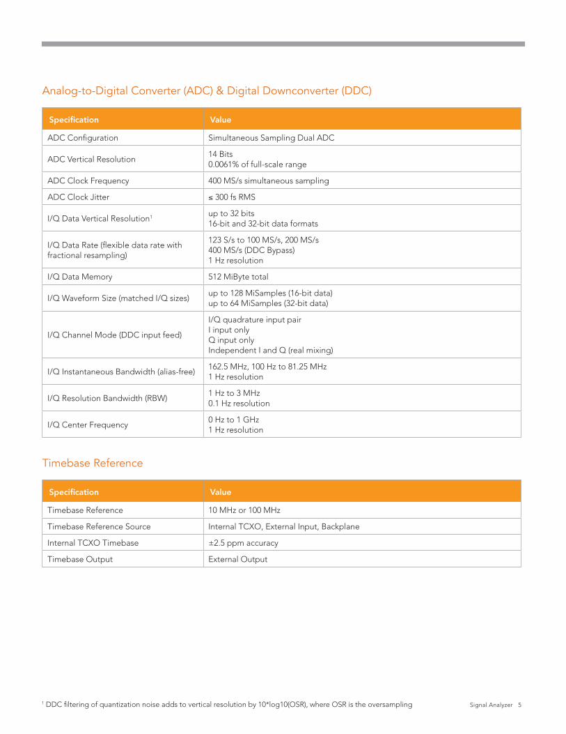
Analog-to-Digital Converter (ADC) & Digital Downconverter (DDC)
Specification Value
ADC Configuration Simultaneous Sampling Dual ADC
ADC Vertical Resolution14 Bits0.0061% of full-scale range
ADC Clock Frequency 400 MS/s simultaneous sampling
ADC Clock Jitter ≤ 300 fs RMS
I/Q Data Vertical Resolution1 up to 32 bits16-bit and 32-bit data formats
I/Q Data Rate (flexible data rate with fractional resampling)
123 S/s to 100 MS/s, 200 MS/s400 MS/s (DDC Bypass)1 Hz resolution
I/Q Data Memory 512 MiByte total
I/Q Waveform Size (matched I/Q sizes)up to 128 MiSamples (16-bit data)up to 64 MiSamples (32-bit data)
I/Q Channel Mode (DDC input feed)
I/Q quadrature input pairI input onlyQ input onlyIndependent I and Q (real mixing)
I/Q Instantaneous Bandwidth (alias-free)162.5 MHz, 100 Hz to 81.25 MHz1 Hz resolution
I/Q Resolution Bandwidth (RBW)1 Hz to 3 MHz0.1 Hz resolution
I/Q Center Frequency0 Hz to 1 GHz1 Hz resolution
Timebase Reference
Specification Value
Timebase Reference 10 MHz or 100 MHz
Timebase Reference Source Internal TCXO, External Input, Backplane
Internal TCXO Timebase ±2.5 ppm accuracy
Timebase Output External Output
1 DDC filtering of quantization noise adds to vertical resolution by 10*log10(OSR), where OSR is the oversampling

Signal Analyzer 6
Trigger
Specification Value
Trigger SourceI, Q, I/Q Envelope, External Input, Pattern, Software, Immediate (no trigger), TTL Trigger 0-7, Star Trigger
Trigger Slope/Polarity Positive or Negative
Trigger Position Pre-Trigger & Post-Trigger
Trigger Jitter ≤ 2.5 ns peak-to-peak
External Input (front panel)
Specification Value
Functionality Trigger Input, Timebase Reference Input
Absolute Maximum Input (no damage) ≤ ± 5 V (DC + peak AC), CAT I
Input Trigger Level Adjustment
-2 V to +2 V0.5 mV resolution≤ 20 mV accuracy20 mV overdrive (input hysteresis)
Input Bandwidth (-3 dB) ≥ 250 MHz
Input Impedance1 MΩ || 30 pF or 50 Ω≤ ±2% accuracy
Connector SMB

Signal Analyzer 7
External Ouput (front panel)
Specification Value
FunctionalityTrigger Output, Timebase Reference Output, Event Output, Programmable Clock Output, Programmable Pulse Output, Constant Level
Output Event SourceTrigger Event, Capture Complete Event, Operation Complete Event, Master Summary Status Event
Polarity High or Low Truth
Programmable Event Pulse Width 50 ns to 163 ms
Programmable ClockPeriod: 26.667 ns to 100 seconds13.333 ns resolution50% Duty Cycle
Programmable PulsePulse Repetition IntervalPulse Width
26.667 ns to 100 seconds, 13.333 ns resolution26.667 ns
Probe Compensation 10 kHz Clock which can be used to compensate probe
Limit Test Successful Event pulse after each capture upon limit or mask test success
Output LevelTTL Compatible into ≥ 200 Ω≥ ±24 mA Output Drive
Output Enable Tri-State Output Capability
Connector SMB
Backplane Triggers
Specification Value
Functionality Multi-Instrument Synchronization Trigger, Event Output Signals
Triggers TTL Trigger 0-7
Direction Input or Output
SourceTrigger Event, Capture Complete Event, Operation Complete Event, Master Summary Status Event, Constant Level
Polarity High or Low Truth
Programmable Event Pulse Width 50 ns to 163 ms

Signal Analyzer 8
Traces
Specification Value
Trace Channels Quantity 8
Trace SizeUp to 512 KiSample32-bit floating point data
Trace Feed (source)Input Channels or Reference Channels
Trace TypeWrite (Live), Average, Max Hold, Min Hold(Reference Feeds use Write Type only)
Trace Average Count 2 to 65535
Trace Data FormatLinear Magnitude, Logarithmic Magnitude, Phase, Real, Imaginary, 32-bit floating point data
Reference Waveforms
Specification Value
Reference Channels Quantity 4
Reference Storage Non-volatile memory storage
Reference Data32 KiSample maximum waveform size32-bit floating point data
Reference Data FormatLinear Magnitude, Logarithmic Magnitude, Phase, Real, Imaginary, 32-bit floating point data
Markers
Specification Value
Marker Channels Quantity 2
Marker Functionality Waveform Trace Magnitude and Frequency Markers
Marker Source Trace 1-8
Marker Peak SearchSearch MethodsSelectable Search Options
Maximum, Next Maximum by Amplitude, Next Maximum Left, Next Maximum RightAbsolute Threshold, Relative Excursion
Signal Analyzer 9
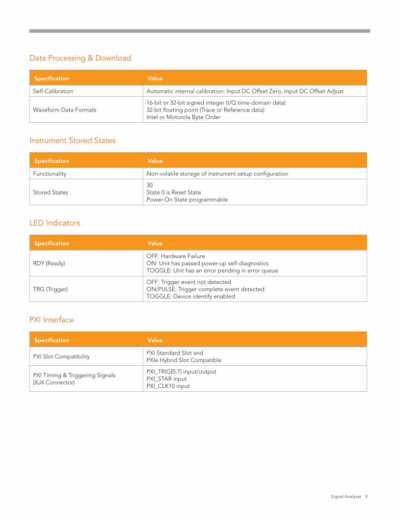
Data Processing & Download
Specification Value
Self-Calibration Automatic internal calibration: Input DC Offset Zero, Input DC Offset Adjust
Waveform Data Formats16-bit or 32-bit signed integer (I/Q time-domain data)32-bit floating point (Trace or Reference data)Intel or Motorola Byte Order
Instrument Stored States
Specification Value
Functionality Non-volatile storage of instrument setup configuration
Stored States30State 0 is Reset StatePower-On State programmable
LED Indicators
Specification Value
RDY (Ready)OFF: Hardware FailureON: Unit has passed power-up self-diagnosticsTOGGLE: Unit has an error pending in error queue
TRG (Trigger)OFF: Trigger event not detectedON/PULSE: Trigger complete event detectedTOGGLE: Device identify enabled
PXI Interface
Specification Value
PXI Slot CompatibilityPXI Standard Slot and PXIe Hybrid Slot Compatible
PXI Timing & Triggering Signals (XJ4 Connector)
PXI_TRIG[0:7] input/outputPXI_STAR inputPXI_CLK10 input
Signal Analyzer 10
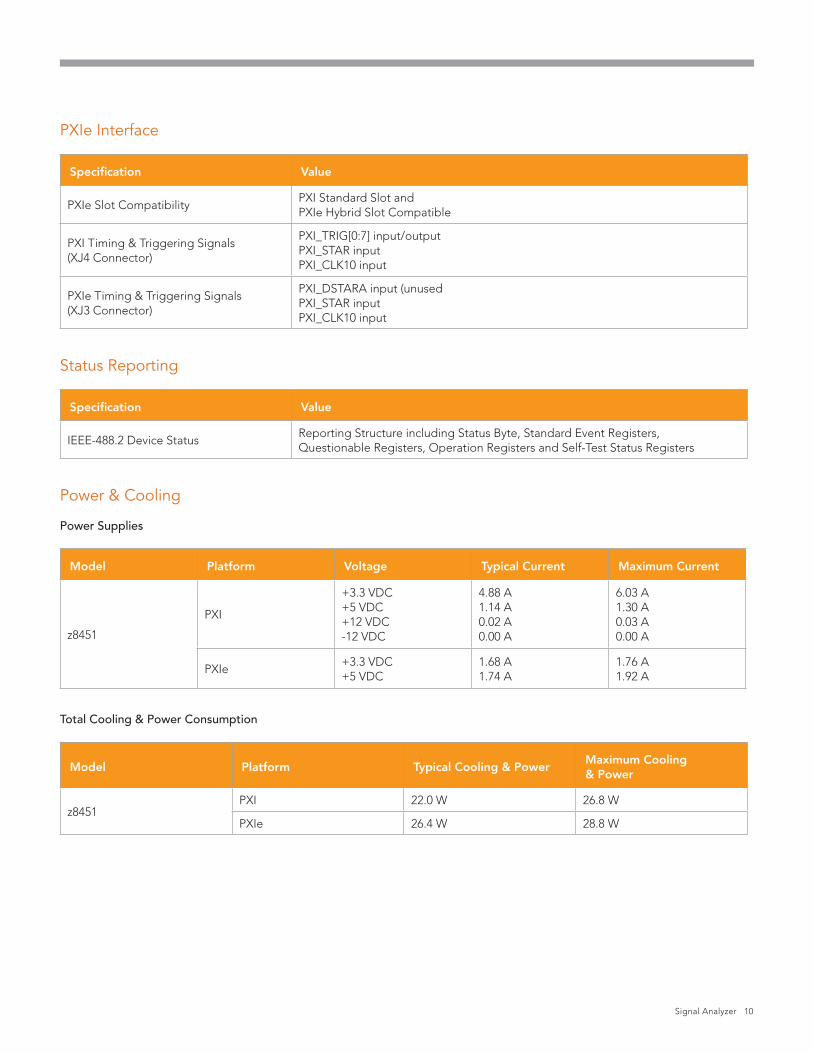
PXIe Interface
Specification Value
PXIe Slot CompatibilityPXI Standard Slot and PXIe Hybrid Slot Compatible
PXI Timing & Triggering Signals (XJ4 Connector)
PXI_TRIG[0:7] input/outputPXI_STAR inputPXI_CLK10 input
PXIe Timing & Triggering Signals (XJ3 Connector)
PXI_DSTARA input (unusedPXI_STAR inputPXI_CLK10 input
Status Reporting
Specification Value
IEEE-488.2 Device StatusReporting Structure including Status Byte, Standard Event Registers, Questionable Registers, Operation Registers and Self-Test Status Registers
Power & Cooling
Power Supplies
Model Platform Voltage Typical Current Maximum Current
z8451
PXI
+3.3 VDC+5 VDC+12 VDC-12 VDC
4.88 A1.14 A0.02 A0.00 A
6.03 A1.30 A0.03 A0.00 A
PXIe+3.3 VDC+5 VDC
1.68 A1.74 A
1.76 A1.92 A
Total Cooling & Power Consumption
Model Platform Typical Cooling & Power Maximum Cooling & Power
z8451PXI 22.0 W 26.8 W
PXIe 26.4 W 28.8 W
Signal Analyzer 11
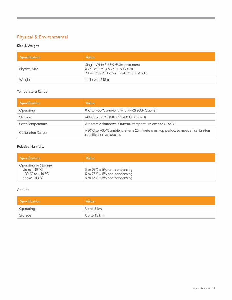
Physical & Environmental
Size & Weight
Specification Value
Physical SizeSingle-Wide 3U PXI/PXIe Instrument8.25” x 0.79” x 5.25” (L x W x H)20.96 cm x 2.01 cm x 13.34 cm (L x W x H)
Weight 11.1 oz or 315 g
Temperature Range
Specification Value
Operating 0°C to +50°C ambient (MIL-PRF28800F Class 3)
Storage -40°C to +75°C (MIL-PRF28800F Class 3)
Over-Temperature Automatic shutdown if internal temperature exceeds +65°C
Calibration Range+20°C to +30°C ambient, after a 20 minute warm-up period, to meet all calibration specification accuracies
Relative Humidity
Specification Value
Operating or StorageUp to +30 °C+30 °C to +40 °Cabove +40 °C
5 to 95% ± 5% non-condensing5 to 75% ± 5% non-condensing5 to 45% ± 5% non-condensing
Altitude
Specification Value
Operating Up to 5 km
Storage Up to 15 km

Signal Analyzer 12
Terminology
Numeric Prefixes
When referring to numeric values, this document will use SI (International System of Units) and IEC (International Electrotechnical Commission) standard prefixes. Prefix definitions are in the following table.
Prefix Multiplier
n (nano) 1/(1000x1000x1000)
μ (micro) 1/(1000x1000)
m (milli) 1/1000
k/K (kilo) 1000
M (Mega) 1000x1000
G (Giga) 1000x1000x1000
Ki (Kibi) 1024
Mi (Mebi) 1024x1024
Gi (Gibi) 1024x1024x1024
Differential Outputs
Single-Ended is used to refer to the output on either the + or – output pin
Differential is used to refer to the output between the + and- output pins
Vd indicates Volts differential
Vppd indicates Volts peak-to-peak differential

Signal Analyzer 13
Safety
This product is designed to meet the requirements of the following standard of safety for electrical equipment for measurement, control and laboratory use: EN 61010-1
Electromagnetic Compatibility
CE Marking EN 61326-1:1997 with A1:1998 and A2:2001 Compliant
FCC Part 15 (Class A) Compliant
Emissions
EN 55011 Radiated Emissions, ISM Group 1, Class A, distance 10 m, emissions < 1 GHzEN 55011 Conducted Emissions, Class A, emissions < 30 MHz ImmunityEN 61000-4-2 Electrostatic Discharge (ESD), 4 kV by Contact, 8 kV by AirEN 61000-4-3 RF Radiated Susceptibility, 10 V/mEN 61000-4-4 Electrical Fast Transient Burst (EFTB), 2 kV AC Power LinesEN 61000-4-5 SurgeEN 61000-4-6 Conducted ImmunityEN 61000-4-8 Power Frequency Magnetic Field, 30 A/mEN 61000-4-11 Voltage Dips and Interrupts
CE Compliance
This product meets the necessary requirements of applicable European Directives for CE Marking as follows:
73/23/EEC Low Voltage Directive (Safety)89/336/EEC Electromagnetic Compatibility Directive (EMC)
See Declaration of Conformity for this product for additional regulatory compliance information.
Copyright © 2016 LitePoint, A Teradyne Company.
All rights reserved
RESTRICTED RIGHTS LEGENDNo part of this document may bereproduced, transmitted, transcribed,stored in a retrieval system, or translated into any language or computer language, in any form or by any means, electronic, mechanical, magnetic, optical, chemical, manual, or otherwise, without the prior written permission of LitePoint Corporation.
DISCLAIMERLitePoint Corporation makes norepresentations or warranties withrespect to the contents of this manual or of the associated LitePoint Corporation products, and specifically disclaims any implied warranties of merchantability or fitness for any particular purpose. LitePoint Corporation shall under nocircumstances be liable for incidentalor consequential damages or relatedexpenses resulting from the use of thisproduct, even if it has been notified ofthe possibility of such damages.
If you find errors or problems with thisdocumentation, please notify LitePointCorporation at the address listedbelow. LitePoint Corporation does notguarantee that this document is error-free. LitePoint Corporation reserves theright to make changes in specificationsand other information contained in thisdocument without prior notice.
CONTACT INFORMATIONLitePoint Corporation965 W. Maude Ave.Sunnyvale, CA 94085-2803United States of America Telephone: +1.408.456.5000
LITEPOINT TECHNICAL SUPPORTwww.litepoint.com/support
Doc: 1075-1003-001 May 2016 Rev 2
TRADEMARKSLitePoint and the LitePoint logo are registered trademarks of LitePoint Corporation. z8451 is a trademark of LitePoint Corporation. All other trademarks or registered trademarks are owned by their respective owners.
Top Related