


Languages
Pages
Legal

JOURNAL OF MICROELECTROMECHANICAL SYSTEMS, VOL. 20, NO. 4, AUGUST 2011 885
Wafer-to-Wafer Alignment for Three-DimensionalIntegration: A Review
Sang Hwui Lee, Kuan-Neng Chen, Member, IEEE, and James Jian-Qiang Lu, Fellow, IEEE
Abstract—This paper presents a review of the wafer-to-waferalignment used for 3-D integration. This technology is an im-portant manufacturing technique for advanced microelectronicsand microelectromechanical systems, including 3-D integratedcircuits, advanced wafer-level packaging, and microfluidics.Commercially available alignment tools provide prebondingwafer-to-wafer misalignment tolerances on the order of 0.25 µm.However, better alignment accuracy is required for increasingdemands for higher density of through-strata vias and bondedinterstrata vias, whereas issues with wafer-level alignment uni-formity and reliability still remain. Three-dimensional processesalso affect the alignment accuracy, although the misalignmentcould be reduced to certain extent by process control. This paperprovides a comprehensive review of current research activitiesover wafer-to-wafer alignment, including alignment methods, ac-curacy requirements, and possible misalignments and fundamen-tal issues. Current misalignment concerns of the major bondingapproaches are discussed with detailed alignment results. The fun-damental issues associated with wafer alignment are addressed,such as alignment mechanisms, uniformity, reproducibility, ther-mal mismatch, and materials. Alternative alignment approachesare discussed, and perspectives for wafer-to-wafer alignment aregiven. [2010-0363]
Index Terms—Alignment, 3-D integration, wafer bonding,wafer-level packaging.
I. INTRODUCTION
THERE IS a greatly increased demand for ever high-performance high-functionality integration driven by
computation, mobile, and game industries [1]–[8]. Histori-cally, it has been satisfied by downscaling transistors followingMoore’s law. However, the interconnect RC delay has becomea major source of circuit delays as the size of transistorsgets reduced with ever increasing integration scale. Three-dimensional integration has been introduced, developed, andrecognized as one of the solutions in the International Tech-nology Roadmap for Semiconductors in reducing the lengthof interconnects and, furthermore, in satisfying the demand of
Manuscript received December 30, 2010; revised March 11, 2011; acceptedMarch 26, 2011. Date of publication June 9, 2011; date of current versionAugust 3, 2011. This work was supported in part by DARPA, in part byMARCO, and in part NYSTAR through Focus-Center NY: Rensselaer. SubjectEditor D. D. Cho.
S. H. Lee is with the Laboratory for Physical Sciences, College Park, MD21029 USA (e-mail: leesh@ lps.umd.edu).
K.-N. Chen is with the Department of Electronics Engineering, Na-tional Chiao Tung University, Hsinchu 300, Taiwan (e-mail: [email protected]).
J. J.-Q. Lu is with the Department of Electrical, Computer, and SystemsEngineering, Rensselaer Polytechnic Institute, Troy, NY 12180 USA (e-mail:[email protected]).
Color versions of one or more of the figures in this paper are available onlineat http://ieeexplore.ieee.org.
Digital Object Identifier 10.1109/JMEMS.2011.2148161
highly integrated electronic systems [1]–[24]. Whereas conven-tional integration connects circuits horizontally with long inter-connection wires on one substrate, 3-D integration provides anew paradigm to vertically integrate various building blocks.Not only can 3-D integration shorten wires with smaller chipsizes, but also it is a new technology platform for heterogeneousintegration by stacking and connecting dissimilar materials ordifferent modules on one substrate.
Three-dimensional integration has emerged as a promisingsolution in driving the next generation of CMOS integra-tion technology [1]–[20] and microelectromechanical systems(MEMS) [21]–[23]. The major processing of 3-D integrationis composed of four basic unit processes: alignment, bonding,thinning, and interstrata interconnection [1]–[4]. Theseprocesses are under intensive development. For alignment,higher reliable alignment accuracy is required for higher den-sity of through-strata vias (TSVs) and bonded interstrata vias(BISVs). For bonding, robust bonding interface and thermalmanagement are quite challenging. For thinning, uniformity isa critical issue, whereas handling thinned wafers is difficult forsome 3-D integration schemes. For interstrata interconnection,TSV technology has already been used for certain applicationssuch as CMOS imagers, and various TSV technologies arebeing developed [14], [16], [19], [21], [23].
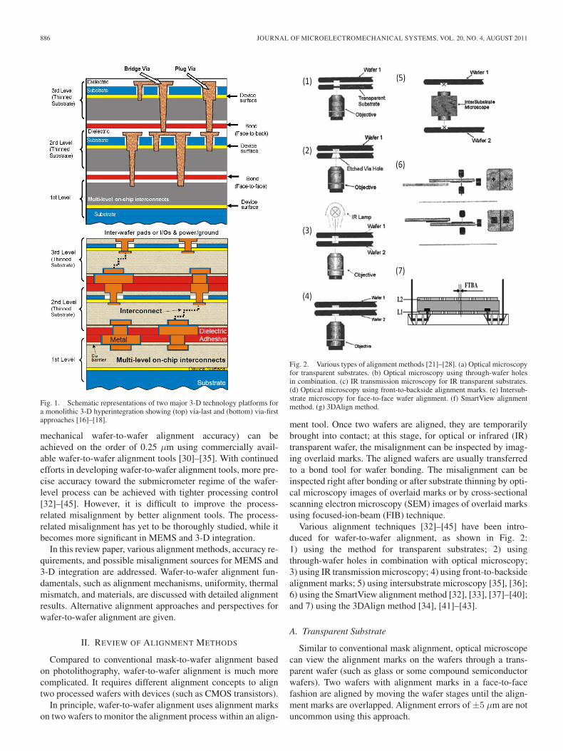
There are several 3-D technology platforms proposed[1]–[4], [10], [18], [24]–[28]. Fig. 1 schematically shows two3-D platforms, i.e., via-first [28] and via-last [24]–[27]. Theyare classified by the sequence order of interstrata intercon-nection formation and wafer bonding. When wafer bonding isahead of interstrata interconnection formation using TSVs, it iscalled “via-last.” After two fully processed wafers are bonded,TSVs are formed to connect the top and bottom circuits. For thevia-first 3-D process platform, a redistributed layer is formedon top of the fully processed device wafer. The redistributionlayers are bonded directly face-to-face using BISVs. Depend-ing on their applications, these platforms may use differentmaterials, for example, for TSV formation, planarization onredistribution layer, alignment, and bonding dissimilar wafers[29], [30]. Various issues on wafer-level 3-D integration havebeen addressed [1]–[4], [10], [13], [31]. Among major 3-Dprocesses, accurate alignment is essential between the bondedwafers to realize a high density of interstrata interconnects (i.e.,TSVs and BISVs) and high volume throughput.
Historically, aligned wafer-to-wafer bonding was devel-oped originally for MEMS process. Today, it is an impor-tant manufacturing technique not only for 3-D integration butalso for advanced wafer-level packaging and microfluidics.The prebonding wafer-to-wafer alignment accuracy (i.e., pure
1057-7157/$26.00 © 2011 IEEE
886 JOURNAL OF MICROELECTROMECHANICAL SYSTEMS, VOL. 20, NO. 4, AUGUST 2011
Fig. 1. Schematic representations of two major 3-D technology platforms fora monolithic 3-D hyperintegration showing (top) via-last and (bottom) via-firstapproaches [16]–[18].
mechanical wafer-to-wafer alignment accuracy) can beachieved on the order of 0.25 µm using commercially avail-able wafer-to-wafer alignment tools [30]–[35]. With continuedefforts in developing wafer-to-wafer alignment tools, more pre-cise accuracy toward the submicrometer regime of the wafer-level process can be achieved with tighter processing control[32]–[45]. However, it is difficult to improve the process-related misalignment by better alignment tools. The process-related misalignment has yet to be thoroughly studied, while itbecomes more significant in MEMS and 3-D integration.
In this review paper, various alignment methods, accuracy re-quirements, and possible misalignment sources for MEMS and3-D integration are addressed. Wafer-to-wafer alignment fun-damentals, such as alignment mechanisms, uniformity, thermalmismatch, and materials, are discussed with detailed alignmentresults. Alternative alignment approaches and perspectives forwafer-to-wafer alignment are given.
II. REVIEW OF ALIGNMENT METHODS
Compared to conventional mask-to-wafer alignment basedon photolithography, wafer-to-wafer alignment is much morecomplicated. It requires different alignment concepts to aligntwo processed wafers with devices (such as CMOS transistors).
In principle, wafer-to-wafer alignment uses alignment markson two wafers to monitor the alignment process within an align-
Fig. 2. Various types of alignment methods [21]–[28]. (a) Optical microscopyfor transparent substrates. (b) Optical microscopy using through-wafer holesin combination. (c) IR transmission microscopy for IR transparent substrates.(d) Optical microscopy using front-to-backside alignment marks. (e) Intersub-strate microscopy for face-to-face wafer alignment. (f) SmartView alignmentmethod. (g) 3DAlign method.
ment tool. Once two wafers are aligned, they are temporarilybrought into contact; at this stage, for optical or infrared (IR)transparent wafer, the misalignment can be inspected by imag-ing overlaid marks. The aligned wafers are usually transferredto a bond tool for wafer bonding. The misalignment can beinspected right after bonding or after substrate thinning by opti-cal microscopy images of overlaid marks or by cross-sectionalscanning electron microscopy (SEM) images of overlaid marksusing focused-ion-beam (FIB) technique.
Various alignment techniques [32]–[45] have been intro-duced for wafer-to-wafer alignment, as shown in Fig. 2:1) using the method for transparent substrates; 2) usingthrough-wafer holes in combination with optical microscopy;3) using IR transmission microscopy; 4) using front-to-backsidealignment marks; 5) using intersubstrate microscopy [35], [36];6) using the SmartView alignment method [32], [33], [37]–[40];and 7) using the 3DAlign method [34], [41]–[43].
A. Transparent Substrate
Similar to conventional mask alignment, optical microscopecan view the alignment marks on the wafers through a trans-parent wafer (such as glass or some compound semiconductorwafers). Two wafers with alignment marks in a face-to-facefashion are aligned by moving the wafer stages until the align-ment marks are overlapped. Alignment errors of ±5 µm are notuncommon using this approach.
LEE et al.: WAFER-TO-WAFER ALIGNMENT FOR THREE-DIMENSIONAL INTEGRATION: A REVIEW 887
B. Through-Wafer Holes
As shown in Fig. 2(b), the alignment marks on one of thealigning wafers can be seen through the holes drilled or etchedon the other. The dimension and position of the through-holesare very critical in this approach since the wafer with holesdoes not have particular alignment marks. It is very difficultfor drilling and etching to reach the precise micrometer-levelaccuracy of the via-hole dimensions through the wafer substrate(e.g., ∼725-µm thickness for 200-mm silicon wafers). Thistechnique is hardly to reach micrometer-level wafer-to-waferalignment.
C. IR Transmission Microscopy
Instead of a visible light, an IR light is placed on one sideof the wafer (opposite to the optical microscope), as shownin Fig. 2(c). Silicon wafers can be aligned since silicon istransparent to IR light. However, it is limited to the siliconwafers with polished double side surfaces. Alignment errorscould be as small as ±1 µm with this approach. However, theview is distorted by nontransparency of metal or heavily dopedsilicon layer.
D. Backside Alignment With Digitalized Image
Alignment marks are placed on the frontside (bond) of thefirst wafer and on the backside (counter-bond) of the secondwafer. Similar to a mask aligner, alignment marks on the firstwafer—face down toward the bottom microscope—is capturedand stored as a digitalized image. The second wafer—bond faceupward and alignment mark downward—is moved in betweenthe first wafer and the microscope. The alignment marks on thebackside of the second wafer are viewed and aligned with thestored image of the alignment mark on the first wafer. Analignment tolerance of ±5 µm can be reached. It is critical toregister well the alignment marks on the backside of the secondwafer.
E. SmartView Alignment Method
Two pairs of microscopes (one pair on the “left” side andthe other on the “right” side of the aligning wafers) are placedoutside of the top and bottom wafers. The aligning wafersare placed “face-to-face” with a gap of less than 100 µm andvacuum-sucked on the top and bottom wafer stages, respec-tively. The two wafer stages can be moved back and forthhorizontally. After the pair of top and bottom microscopes arealigned with each other (i.e., calibrated), the bottom wafer stageis moved inbetween the pairs of microscopes; the marks in thetop microscopes are aligned to the alignment marks on thebottom wafer. The bottom wafer position is stored, andthe bottom stage is retreated. The top wafer stage is movedto the position against the bottom microscopes. The align-ment marks on the top wafer are then aligned to the bottommicroscopes. The bottom wafer stage is moved back to itsstored alignment position. Finally, the two aligned wafers arevertically moved to contact each other and are clamped tohold the alignment for wafer bonding. Misalignment tolerances
can be achieved on the order of 0.25 µm in this method [32],[33], [36].
F. 3DAlign Method
It comprises two microscope sets and a modified wafer table.For double side aligning, one set views directly down to thefrontside of a wafer and another set views through a specialmirror like a modified periscope to the bottom side, as shown inFig. 2(g). To align a wafer pair, the second microscope set viewsthe bottom side of the second wafer. Two viewed images areoverlaid and aligned. A submicrometer misalignment tolerancewas demonstrated with this method [34], [42], [43].
III. ALIGNMENT CONSIDERATION ON 3-D PLATFORMS
Unlike conventional mask alignment in photolithography, theaddition of a fully processed wafer or a handling glass wafermakes alignment more complicated. The alignment approachesdescribed in Section II must be considered with each 3-D plat-form. Alignment marks and bond surface should be designedin advance for a given 3-D platform. Moreover, wafer bondingmay cause further misalignment. Two alignment approachespossible for 3-D platforms [31], [41] are considered here in thispaper: 1) face-to-face and 2) face-to-back.
A. Face-to-Face
At the bonding interface, the alignment marks on one waferface the ones on the other wafer. In this case, alignment markscan be fabricated on the layer of top global interconnects. Thealignment marks can also be fabricated on the CMOS layerif the frontside of the wafer is bonded on a temporary handlewafer (silicon or glass) and if the bulk silicon substrate of thiswafer is removed. It is possible to view the aligning marks in aconventional mask alignment microscope only if a transparentwafer substrate is used (such as glass wafer using visible lightor silicon wafer using IR). In this case, the alignment marks canbe fabricated on either the layer of top global interconnects orthe CMOS layer. With a nontransparent silicon substrate, thereare a few ways to overlay the marks in this aligning method.SmartView, IR microscope, and intermicroscope are practicallyused for the face-to-face wafer alignment.
B. Face-to-Back
The alignment marks on both bonding wafers face towarda microscope, which means that the alignment marks on onewafer do not face those on the other wafer at the bondinginterface. The backside alignment with digitalized image (asdiscussed in Section II-D) can be used with an optical mi-croscope. With this approach, it is difficult to inspect thepostbonding alignment accuracy with IR since the alignmentmarks on both wafers are not on the same focal plane. The face-to-face alignment method can also be used if alignment marksare fabricated on the backside of one wafer, although it is quitechallenging to realize the alignment marks that are well alignedto the circuits on the wafer frontside.
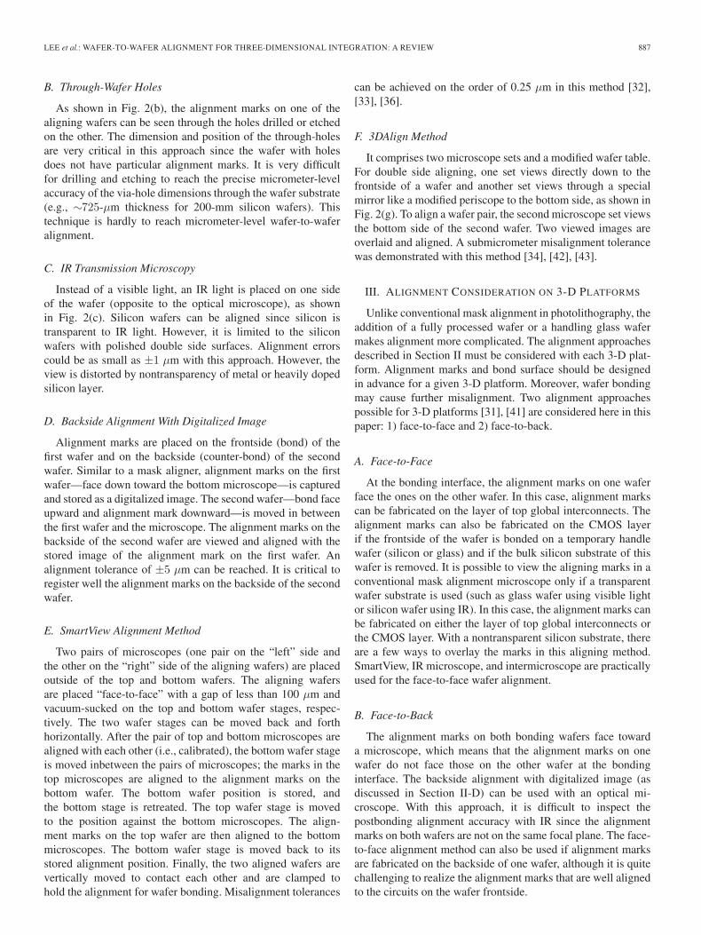
888 JOURNAL OF MICROELECTROMECHANICAL SYSTEMS, VOL. 20, NO. 4, AUGUST 2011
Fig. 3. Schematic of the bonding pads based on the via design rule. L1 and L2
are the diameters of the bonding pads on the first and second wafers, LOverlap
is the minimum overlay between the bonding pads on the first and secondwafers, LPitch is the edge-to-edge distance of the bonding pads on the secondwafer, and LSpace is the distance between two bonding pads on the first wafer.
In all of the 3-D platforms, after alignment, two alignedwafers may experience further thermal/mechanical processessuch as bonding, thinning (grinding and polishing), furtherinterconnect or redistribution layer formation, TSV forma-tion, etc. These thermal/mechanical processes may affect thealignment accuracy obtained during the room-temperaturewafer-to-wafer alignment. Therefore, those processes have tobe evaluated and controlled for 3-D integration.
IV. ALIGNMENT IMPACT ON INTERCONNECT VIA DENSITY
Accurate alignment is a critical factor for high interstratainterconnection via density and multilevel stacking. Interstratainterconnection via density in wafer-level 3-D approach isdirectly related to the performance of the wafer-level alignmenttool and the process control, which determines via pitch andsize. The minimum pitch and overlap via size can be defined asfollows [46]:
LPitch =LSpace + 2 · LOverlap + L2 (1)
LOverlap =MMean + 3 · MSdv + MRun-out (2)
where L2 is the diameter of the bonding pads (as shown inFig. 3), LOverlap is the minimum overlay, LPitch is the edge-to-edge distance of the bonding pads on the second wafer, LSpace
is the distance between two bonding pads on the first wafer,MMean is the mean of the wafer-to-wafer misalignment, MSdv
is the standard deviation of the wafer-to-wafer misalignment,and MRun-out is the maximum run-out misalignment. Themaximum run-out misalignment may be controlled as discussedin the following sections.
For instance, with the current alignment technology, let usconsider that both the mean and the standard deviation are1 µm, and the maximum misalignment within a wafer withthe best wafer bow control is also 1 µm. For the minimumlanding pad size of 5 µm, the pitch size would be calculated as12 µm if both via size and line spacing are 1 µm. The numberof interwafer interconnects in an area of 10 mm2 could be∼2 × 10⁴ when the interstrata interconnection area ratio (i.e.,area of interstrata interconnects/die area) is 1% [9]. However, ifthe mean and standard deviation are 0.25 and 0.1 µm, the pitchsize and the number of interstrata interconnects in the samearea (10 mm2) could be 5.1 µm and ∼6 × 10⁴. The wafer-to-
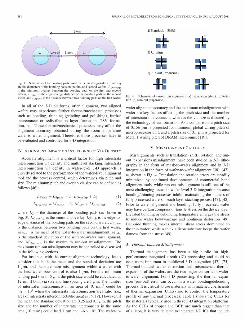
Fig. 4. Schematic of various misalignments. (a) Translation (shift). (b) Rota-tion. (c) Run-out (expansion).
wafer alignment accuracy and the maximum misalignment withwafer are key factors affecting the pitch size and the numberof interstrata interconnects, whereas the via size is dictated bythe technology of via formation. As a comparison, a pitch sizeof 0.156 µm is projected for minimum global wiring pitch ofmicroprocessor unit, and a pitch size of 0.1 µm is projected forMetal 1 wiring pitch of DRAM interconnect [19].
V. MISALIGNMENT CATEGORY
Misalignments, such as translation (shift), rotation, and run-out (expansion) misalignment, have been studied in 2-D litho-graphy in the form of mask-to-wafer alignment and in 3-Dintegration in the form of wafer-to-wafer alignment [38], [47],as shown in Fig. 4. Translation and rotation errors are steadilyminimized by continued developments of commercial bondalignment tools, while run-out misalignment is still one of themost challenging issues in wafer-level 3-D integration becausebonding/thinning processes inhibit maintaining the flatness offully processed wafers in each layer-stacking process [47], [48].Prior to wafer alignment and bonding, fully processed wafermay have certain compress or tensile stress on the device layer.Elevated bonding or debonding temperature enlarges the stressto induce wafer bow/warpage and nonlinear distortion [49].Backside thinning makes internal shear stress dominated tothe thin wafer, while a thick silicon substrate keeps the waferflatness from the stress [49].
A. Thermal-Induced Misalignment
Thermal management has been a big hurdle for high-performance integrated circuit (IC) processing and could beeven more important in multilevel 3-D integration [47]–[75].Thermal-induced wafer distortion and mismatched thermalexpansion of the wafers are the two major concerns in wafer-to-wafer alignment. For 3-D processing, the thermal expan-sion (run-out) error can occur in a wafer bonding/debondingprocess. It is critical to use materials with matched coefficientsof thermal expansion (CTEs) and to control the temperatureprofile of any thermal processes. Table I shows the CTEs forthe materials typically used in these 3-D integration platforms.As the CTEs of copper and BCB are much bigger than thatof silicon, it is very delicate to integrate 3-D ICs that include
LEE et al.: WAFER-TO-WAFER ALIGNMENT FOR THREE-DIMENSIONAL INTEGRATION: A REVIEW 889
TABLE ICTES FOR THE MATERIALS COMMONLY USED IN SOME 3-D PLATFORMS
Fig. 5. Thermal expansion errors due to temperature differentials betweenbonded substrates [47].
copper or BCB. During wafer bonding, the temperatures on thetwo wafers that are to be bonded can be different because thealigned top and bottom wafers are usually heated separately bytop and bottom hotplates. This temperature difference on thetwo wafers can result in different thermal expansions betweenthese two wafers, leading to further misalignment (shown inFig. 5). It is important to keep the bonding temperatures on thebond pair matched to avoid different thermal expansions.
It is also important to make sure that the stress of the devicelayer is released enough, thus reducing any wafer bow, whichcan also result in misalignment. Moreover, glass and siliconsubstrates are often used as transfer carriers. To minimizethe residual stress from previous IC process, a CTE-matchedlow-stress polymer adhesive is required. In wafer bonding ofdissimilar materials, the thermal expansion difference on thebonding pair would be significant; therefore, it is very difficultto keep the alignment unless the bonding process is done atroom temperature or the bonding temperature profiles on thetop and bottom wafers are so controlled to compensate the CTEmismatch.
B. Wafer Stress and Nonlinear Wafer Distortion
Wafer stress and localized wafer thickness variation inducewafer warpage/bow and nonlinear wafer distortion. Backside
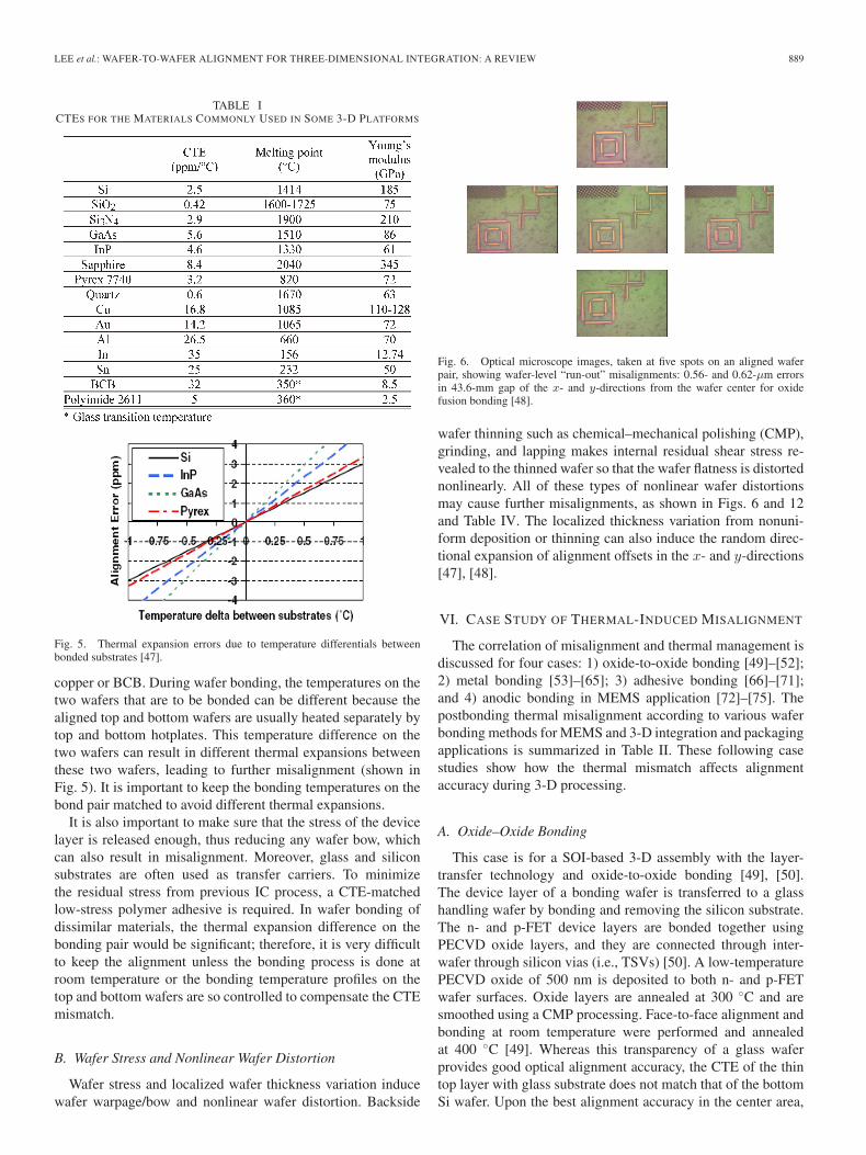
Fig. 6. Optical microscope images, taken at five spots on an aligned waferpair, showing wafer-level “run-out” misalignments: 0.56- and 0.62-µm errorsin 43.6-mm gap of the x- and y-directions from the wafer center for oxidefusion bonding [48].
wafer thinning such as chemical–mechanical polishing (CMP),grinding, and lapping makes internal residual shear stress re-vealed to the thinned wafer so that the wafer flatness is distortednonlinearly. All of these types of nonlinear wafer distortionsmay cause further misalignments, as shown in Figs. 6 and 12and Table IV. The localized thickness variation from nonuni-form deposition or thinning can also induce the random direc-tional expansion of alignment offsets in the x- and y-directions[47], [48].
VI. CASE STUDY OF THERMAL-INDUCED MISALIGNMENT
The correlation of misalignment and thermal management isdiscussed for four cases: 1) oxide-to-oxide bonding [49]–[52];2) metal bonding [53]–[65]; 3) adhesive bonding [66]–[71];and 4) anodic bonding in MEMS application [72]–[75]. Thepostbonding thermal misalignment according to various waferbonding methods for MEMS and 3-D integration and packagingapplications is summarized in Table II. These following casestudies show how the thermal mismatch affects alignmentaccuracy during 3-D processing.
A. Oxide–Oxide Bonding
This case is for a SOI-based 3-D assembly with the layer-transfer technology and oxide-to-oxide bonding [49], [50].The device layer of a bonding wafer is transferred to a glasshandling wafer by bonding and removing the silicon substrate.The n- and p-FET device layers are bonded together usingPECVD oxide layers, and they are connected through inter-wafer through silicon vias (i.e., TSVs) [50]. A low-temperaturePECVD oxide of 500 nm is deposited to both n- and p-FETwafer surfaces. Oxide layers are annealed at 300 ◦C and aresmoothed using a CMP processing. Face-to-face alignment andbonding at room temperature were performed and annealedat 400 ◦C [49]. Whereas this transparency of a glass waferprovides good optical alignment accuracy, the CTE of the thintop layer with glass substrate does not match that of the bottomSi wafer. Upon the best alignment accuracy in the center area,
890 JOURNAL OF MICROELECTROMECHANICAL SYSTEMS, VOL. 20, NO. 4, AUGUST 2011
TABLE IIPOSTBONDING ALIGNMENT ACCURACY IN VARIOUS BONDING
APPROACHES [45], [50], [57], [61], [64], [69], [71]
TABLE IIIMISALIGNMENT RESULTS AFTER BONDING WITH
DIFFERENT PROFILES [53]
the alignment errors become larger toward the edges (so called“run-out”), as shown in Fig. 6. This run-out error due to thermalexpansion can be analyzed by the study of wafer bow in thelayer-transfer process of SOI-based 3-D assembly. The glasshandle wafer is delaminated by a laser ablation technique.Fig. 6 shows the optical microscope images of wafer-level “run-out” misalignments: a 0.6-µm error in 43.6-mm gaps fromthe center. Misalignment is measured over the 200-mm wafersubstrate in postalignment inspection before annealing. Thisrun-out alignment error is caused mainly by the thermal stressof laminating the device layer to a glass handle wafer.
The alignment average (in micrometer), standard deviation(in micrometer), and run-out rate (in micrometer per millime-ter) are measured as 0.16/0.26/0.0128 and 0.02/0.10/0.0156 forthe x- and y-directions, respectively. Here, the run-out rate(in micrometer per millimeter) is defined as a misalignmenterror (in micrometer) over the distance (in millimeter) from thecenter of the wafer. The run-out error (expansion error), evenafter annealing, is 0.56 and 0.62 µm in the x- and y-axes onthe die in the distance of 90 mm from the center, as shown inFig. 6. These run-out errors may be explained as follows: 1) thelarge wafer bows at the steps of postlamination and postbondingfilm preparation caused the expansion mismatch between theglass and silicon device layers along with the large glass waferbow; 2) during the expansion mismatch, a large residual stresswas built on a silicon device layer from the previous steps;3) thus, the patterns in the thin device layer are stretched outduring the wafer bow correction step (preoxide bonding). Mostof the bonding/debonding process involves inevitable thermalprocess. As an example of device layer expansion over a glasshandle wafer during layer-transfer process regardless of glass
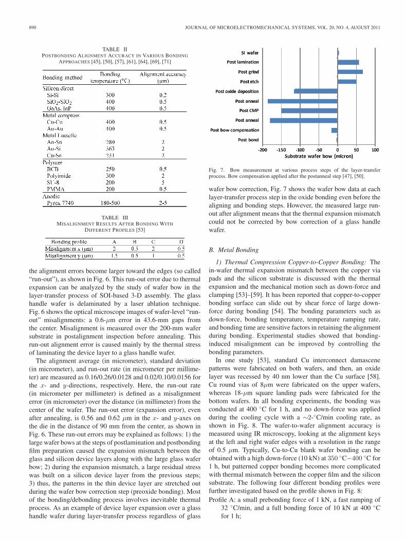
Fig. 7. Bow measurement at various process steps of the layer-transferprocess. Bow compensation applied after the postanneal step [47], [50].
wafer bow correction, Fig. 7 shows the wafer bow data at eachlayer-transfer process step in the oxide bonding even before thealigning and bonding steps. However, the measured large run-out after alignment means that the thermal expansion mismatchcould not be corrected by bow correction of a glass handlewafer.
B. Metal Bonding
1) Thermal Compression Copper-to-Copper Bonding: Thein-wafer thermal expansion mismatch between the copper viapads and the silicon substrate is discussed with the thermalexpansion and the mechanical motion such as down-force andclamping [53]–[59]. It has been reported that copper-to-copperbonding surface can slide out by shear force of large down-force during bonding [54]. The bonding parameters such asdown-force, bonding temperature, temperature ramping rate,and bonding time are sensitive factors in retaining the alignmentduring bonding. Experimental studies showed that bonding-induced misalignment can be improved by controlling thebonding parameters.
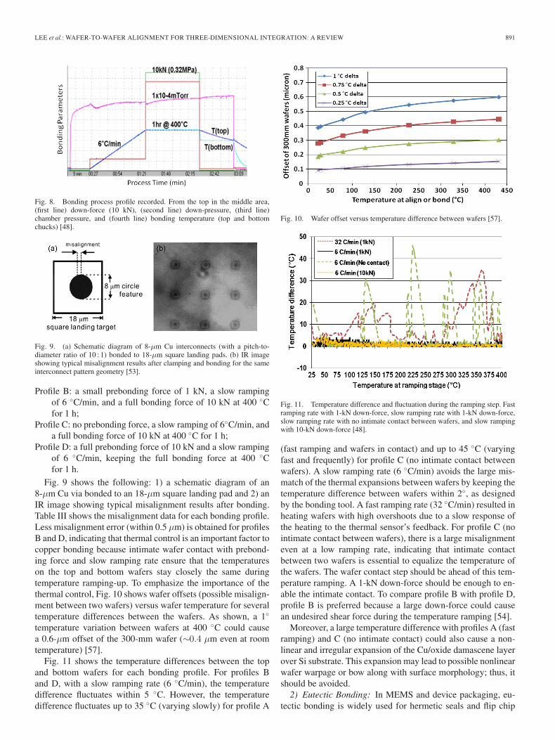
In one study [53], standard Cu interconnect damascenepatterns were fabricated on both wafers, and then, an oxidelayer was recessed by 40 nm lower than the Cu surface [58].Cu round vias of 8µm were fabricated on the upper wafers,whereas 18-µm square landing pads were fabricated for thebottom wafers. In all bonding experiments, the bonding wasconducted at 400 ◦C for 1 h, and no down-force was appliedduring the cooling cycle with a ∼2-◦C/min cooling rate, asshown in Fig. 8. The wafer-to-wafer alignment accuracy ismeasured using IR microscopy, looking at the alignment keysat the left and right wafer edges with a resolution in the rangeof 0.5 µm. Typically, Cu-to-Cu blank wafer bonding can beobtained with a high down-force (10 kN) at 350 ◦C−400 ◦C for1 h, but patterned copper bonding becomes more complicatedwith thermal mismatch between the copper film and the siliconsubstrate. The following four different bonding profiles werefurther investigated based on the profile shown in Fig. 8:Profile A: a small prebonding force of 1 kN, a fast ramping of
32 ◦C/min, and a full bonding force of 10 kN at 400 ◦Cfor 1 h;
LEE et al.: WAFER-TO-WAFER ALIGNMENT FOR THREE-DIMENSIONAL INTEGRATION: A REVIEW 891
Fig. 8. Bonding process profile recorded. From the top in the middle area,(first line) down-force (10 kN), (second line) down-pressure, (third line)chamber pressure, and (fourth line) bonding temperature (top and bottomchucks) [48].
Fig. 9. (a) Schematic diagram of 8-µm Cu interconnects (with a pitch-to-diameter ratio of 10 : 1) bonded to 18-µm square landing pads. (b) IR imageshowing typical misalignment results after clamping and bonding for the sameinterconnect pattern geometry [53].
Profile B: a small prebonding force of 1 kN, a slow rampingof 6 ◦C/min, and a full bonding force of 10 kN at 400 ◦Cfor 1 h;
Profile C: no prebonding force, a slow ramping of 6◦C/min, anda full bonding force of 10 kN at 400 ◦C for 1 h;
Profile D: a full prebonding force of 10 kN and a slow rampingof 6 ◦C/min, keeping the full bonding force at 400 ◦Cfor 1 h.
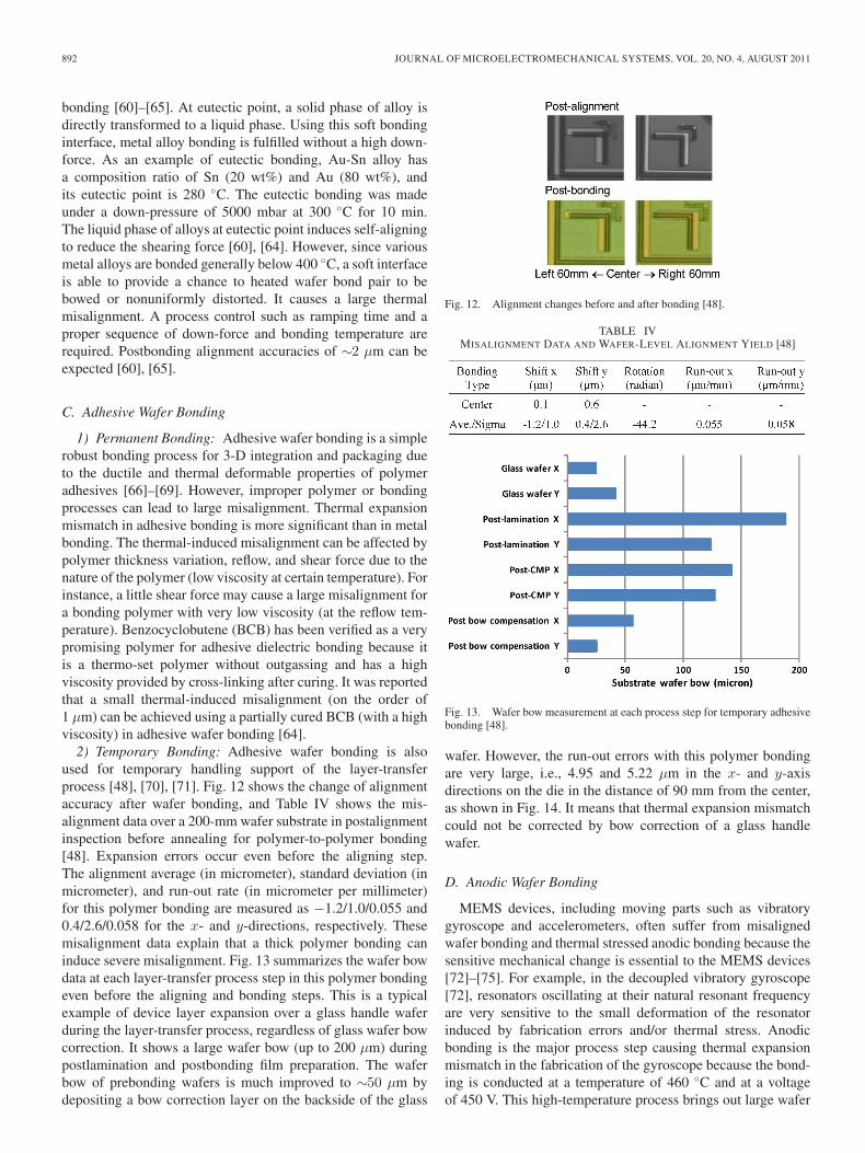
Fig. 9 shows the following: 1) a schematic diagram of an8-µm Cu via bonded to an 18-µm square landing pad and 2) anIR image showing typical misalignment results after bonding.Table III shows the misalignment data for each bonding profile.Less misalignment error (within 0.5 µm) is obtained for profilesB and D, indicating that thermal control is an important factor tocopper bonding because intimate wafer contact with prebond-ing force and slow ramping rate ensure that the temperatureson the top and bottom wafers stay closely the same duringtemperature ramping-up. To emphasize the importance of thethermal control, Fig. 10 shows wafer offsets (possible misalign-ment between two wafers) versus wafer temperature for severaltemperature differences between the wafers. As shown, a 1◦
temperature variation between wafers at 400 ◦C could causea 0.6-µm offset of the 300-mm wafer (∼0.4 µm even at roomtemperature) [57].
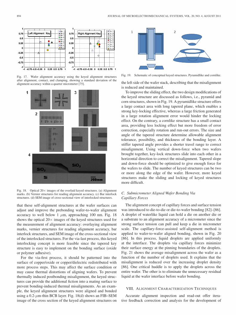
Fig. 11 shows the temperature differences between the topand bottom wafers for each bonding profile. For profiles Band D, with a slow ramping rate (6 ◦C/min), the temperaturedifference fluctuates within 5 ◦C. However, the temperaturedifference fluctuates up to 35 ◦C (varying slowly) for profile A
Fig. 10. Wafer offset versus temperature difference between wafers [57].
Fig. 11. Temperature difference and fluctuation during the ramping step. Fastramping rate with 1-kN down-force, slow ramping rate with 1-kN down-force,slow ramping rate with no intimate contact between wafers, and slow rampingwith 10-kN down-force [48].
(fast ramping and wafers in contact) and up to 45 ◦C (varyingfast and frequently) for profile C (no intimate contact betweenwafers). A slow ramping rate (6 ◦C/min) avoids the large mis-match of the thermal expansions between wafers by keeping thetemperature difference between wafers within 2◦, as designedby the bonding tool. A fast ramping rate (32 ◦C/min) resulted inheating wafers with high overshoots due to a slow response ofthe heating to the thermal sensor’s feedback. For profile C (nointimate contact between wafers), there is a large misalignmenteven at a low ramping rate, indicating that intimate contactbetween two wafers is essential to equalize the temperature ofthe wafers. The wafer contact step should be ahead of this tem-perature ramping. A 1-kN down-force should be enough to en-able the intimate contact. To compare profile B with profile D,profile B is preferred because a large down-force could causean undesired shear force during the temperature ramping [54].
Moreover, a large temperature difference with profiles A (fastramping) and C (no intimate contact) could also cause a non-linear and irregular expansion of the Cu/oxide damascene layerover Si substrate. This expansion may lead to possible nonlinearwafer warpage or bow along with surface morphology; thus, itshould be avoided.
2) Eutectic Bonding: In MEMS and device packaging, eu-tectic bonding is widely used for hermetic seals and flip chip
892 JOURNAL OF MICROELECTROMECHANICAL SYSTEMS, VOL. 20, NO. 4, AUGUST 2011
bonding [60]–[65]. At eutectic point, a solid phase of alloy isdirectly transformed to a liquid phase. Using this soft bondinginterface, metal alloy bonding is fulfilled without a high down-force. As an example of eutectic bonding, Au-Sn alloy hasa composition ratio of Sn (20 wt%) and Au (80 wt%), andits eutectic point is 280 ◦C. The eutectic bonding was madeunder a down-pressure of 5000 mbar at 300 ◦C for 10 min.The liquid phase of alloys at eutectic point induces self-aligningto reduce the shearing force [60], [64]. However, since variousmetal alloys are bonded generally below 400 ◦C, a soft interfaceis able to provide a chance to heated wafer bond pair to bebowed or nonuniformly distorted. It causes a large thermalmisalignment. A process control such as ramping time and aproper sequence of down-force and bonding temperature arerequired. Postbonding alignment accuracies of ∼2 µm can beexpected [60], [65].
C. Adhesive Wafer Bonding
1) Permanent Bonding: Adhesive wafer bonding is a simplerobust bonding process for 3-D integration and packaging dueto the ductile and thermal deformable properties of polymeradhesives [66]–[69]. However, improper polymer or bondingprocesses can lead to large misalignment. Thermal expansionmismatch in adhesive bonding is more significant than in metalbonding. The thermal-induced misalignment can be affected bypolymer thickness variation, reflow, and shear force due to thenature of the polymer (low viscosity at certain temperature). Forinstance, a little shear force may cause a large misalignment fora bonding polymer with very low viscosity (at the reflow tem-perature). Benzocyclobutene (BCB) has been verified as a verypromising polymer for adhesive dielectric bonding because itis a thermo-set polymer without outgassing and has a highviscosity provided by cross-linking after curing. It was reportedthat a small thermal-induced misalignment (on the order of1 µm) can be achieved using a partially cured BCB (with a highviscosity) in adhesive wafer bonding [64].
2) Temporary Bonding: Adhesive wafer bonding is alsoused for temporary handling support of the layer-transferprocess [48], [70], [71]. Fig. 12 shows the change of alignmentaccuracy after wafer bonding, and Table IV shows the mis-alignment data over a 200-mm wafer substrate in postalignmentinspection before annealing for polymer-to-polymer bonding[48]. Expansion errors occur even before the aligning step.The alignment average (in micrometer), standard deviation (inmicrometer), and run-out rate (in micrometer per millimeter)for this polymer bonding are measured as −1.2/1.0/0.055 and0.4/2.6/0.058 for the x- and y-directions, respectively. Thesemisalignment data explain that a thick polymer bonding caninduce severe misalignment. Fig. 13 summarizes the wafer bowdata at each layer-transfer process step in this polymer bondingeven before the aligning and bonding steps. This is a typicalexample of device layer expansion over a glass handle waferduring the layer-transfer process, regardless of glass wafer bowcorrection. It shows a large wafer bow (up to 200 µm) duringpostlamination and postbonding film preparation. The waferbow of prebonding wafers is much improved to ∼50 µm bydepositing a bow correction layer on the backside of the glass
Fig. 12. Alignment changes before and after bonding [48].
TABLE IVMISALIGNMENT DATA AND WAFER-LEVEL ALIGNMENT YIELD [48]
Fig. 13. Wafer bow measurement at each process step for temporary adhesivebonding [48].
wafer. However, the run-out errors with this polymer bondingare very large, i.e., 4.95 and 5.22 µm in the x- and y-axisdirections on the die in the distance of 90 mm from the center,as shown in Fig. 14. It means that thermal expansion mismatchcould not be corrected by bow correction of a glass handlewafer.
D. Anodic Wafer Bonding
MEMS devices, including moving parts such as vibratorygyroscope and accelerometers, often suffer from misalignedwafer bonding and thermal stressed anodic bonding because thesensitive mechanical change is essential to the MEMS devices[72]–[75]. For example, in the decoupled vibratory gyroscope[72], resonators oscillating at their natural resonant frequencyare very sensitive to the small deformation of the resonatorinduced by fabrication errors and/or thermal stress. Anodicbonding is the major process step causing thermal expansionmismatch in the fabrication of the gyroscope because the bond-ing is conducted at a temperature of 460 ◦C and at a voltageof 450 V. This high-temperature process brings out large wafer
LEE et al.: WAFER-TO-WAFER ALIGNMENT FOR THREE-DIMENSIONAL INTEGRATION: A REVIEW 893
Fig. 14. Wafer-level misalignments. Optical images taken at nine spots on thewafer along the x- and y-directions, showing misalignments due to the processof layer-transfer using polymer adhesive. 4.95- and 5.22-µm errors in 90-mmgap of the x- and y-directions for polymer bonding [45].
Fig. 15. Wafer warpage of the SOI wafer bonded to glass with increasingbonding temperature [72].
bowing, degrading the device performance. Fig. 15 shows thebonding temperature dependence of wafer warpage. The waferbowing increases up to 80 µm as the bonding temperatureelevates to 460 ◦C, while the bowing is 10 µm at 330 ◦C.Alignment accuracy can be achieved within ±5 µm in the bowof 10 µm of silicon/glass anodic bonding. For a certain materialsuch as 7070 glass, it induces bowing itself when bondingtemperature reaches the strain point. The bow is in the oppositedirection to the bow due to thermal expansion mismatch. Thisis used for bow control [75].
VII. TECHNIQUES TO ALIGNMENT ACCURACY
IMPROVEMENT
In order to reach or keep submicrometer alignment accuracy,better alignment tools are obviously required. Some possiblesolutions [5], [76]–[90] have been developed to prevent orreduce large misalignment, including thermally distorted mis-alignment in terms of process control.
A. Surface Heating
A temperature control unit can be employed to the align-ment process. For example, if the top and bottom chucks are
Fig. 16. Schematic drawing for a conceptual mechanical interlocking mecha-nism. (a) Tapered surfaces slide in the misalignment range. (b) Key structuresare interlocked [75].
heated separately, the stressed wafer warpage could be relaxedtemporarily before in-contact. Local or global surface heatingcompensates the different wafer warpage of two aligning waferscorrecting the expansion offset [5].
B. Mechanical Interlocking
1) Anisotropic Etched Silicon Structure in MEMS: Usingthe anisotropic (KOH) etching of silicon, the concept of matingpyramid (convex) and groove (concave) elements can be usedto improve the wafer alignment accuracy down to a few mi-crometers and better as a passive mechanical wafer alignmenttechnique by sliding to mate and locking the structure [76],[77]. Potential applications of this technique are precisionalignment for bonding of multiwafer MEMS devices and 3-DICs, as well as one-step alignment for simultaneous bonding ofmultiple wafer stacks. Alignment accuracy can be achieved asbetter than 200 nm at the bonding interface [77].
2) Transfer–Join Approach: In this approach [6], [78], thepillarlike copper key structure (Cu stud) is plugged intopolymer-pocketed copper pads. The pocketlike lock is providedat the bottom with a Cu pad that is to be bonded to theCu stud later. The stud and the combined thickness of theadhesive and the insulator are adjusted so that the Cu-stud-to-Cu-pad contact is first established during the bonding to forma metal–metal bond. Under the continued bonding pressure,the stud height is compressed, and the adhesive is brought intocontact with the opposing insulator surface and bonded. Thereis no sliding guideline between the stud and the pad. Only thepolymer window to the pad keeps the stud from later expansionmisalignment. For this approach, the bottom lock structures aredesigned to be larger than the key structures. Therefore, there isroom to accommodate misalignment during operation.
3) Tapered Keyed Structures: Similar to the anisotropicetched silicon structures in MEMS, a tapered structure on thebonding surface can be created to interlock the wafers mechan-ically [79]. The conceptual mechanism [80] is that the keyedstructures can slide into each other along the tapered planes andare mechanically interlocked so that it can prevent wafers fromshifting relative to each other and so that wafers can maintaintheir aligned position during the bonding process. Fig. 16shows a conceptual mechanical interlocking mechanism: 1) thetapered surfaces slide in the misalignment range, and 2) thekey structures are interlocked. The measured alignment accu-racies are shown in Fig. 17. Preliminary results also indicate
894 JOURNAL OF MICROELECTROMECHANICAL SYSTEMS, VOL. 20, NO. 4, AUGUST 2011
Fig. 17. Wafer alignment accuracy using the keyed alignment structuresafter alignment, contact, and clamping, showing a standard deviation of thealignment accuracy within a quarter micrometer [75].
Fig. 18. Optical 20× images of the overlaid keyed structures. (a) Alignmentmarks. (b) Vernier structures for reading alignment accuracy. (c) Bar interlockstructures. (d) SEM image of cross-sectional view of interlocked structures.
that these self-alignment structures at the wafer surfaces canadjust and improve the prebonding wafer-to-wafer alignmentaccuracy to well below 1 µm, approaching 100 nm. Fig. 18shows the optical 20× images of the keyed structures used forthe measurement of alignment accuracy: overlaying alignmentmarks, vernier structures for reading alignment accuracy, barinterlock structures, and SEM image of the cross-sectional viewof the interlocked structures. For the via-last process, this keyedinterlocking concept is more feasible since the tapered keystructure is easy to implement on the bonding surface (oxideor polymer adhesive).
For the via-first process, it should be patterned into thesurface of copper/oxide or copper/dielectric redistributed withmore process steps. This may affect the surface condition ormay cause thermal distortions of aligning wafers. To preventthermally induced postbonding misalignment, the keyed struc-tures can provide the additional fiction into a mating surface toprevent bonding-induced thermal misalignments. As an exam-ple, the keyed alignment structures were aligned and bondedusing a 0.2-µm-thin BCB layer. Fig. 18(d) shows an FIB–SEMimage of the cross section of the keyed alignment structures on
Fig. 19. Schematic of conceptual keyed structures. Pyramidlike and cornlike.
the left side of the wafer stack, describing that the misalignmentis reduced and maintained.
To improve the sliding effect, the two design modifications ofthe keyed structure are discussed as follows, i.e., pyramid andcorn structures, shown in Fig. 19. A pyramidlike structure offersa large contact area with long tapered plane, which enables astrong key-locking effective, whereas a large friction generatedin a large rotation alignment error would hinder the lockingeffect. On the contrary, a cornlike structure has a small contactarea, providing less locking effect but more freedom of errorcorrection, especially rotation and run-out errors. The size andangle of the tapered structure determine allowable alignmenttolerance, possibility, and thickness of the bonding layer. Astiffer tapered angle provides a shorter travel range to correctmisalignment. Using vertical down-force when two wafersbrought together, key-lock structures slide into each other in ahorizontal direction to correct the misalignment. Tapered slopeand down-force should be optimized to give enough force forthe wafers to slide. The number of keyed structures can be twoor more along the edge of the wafer. However, more keyedstructures make the sliding and locking of keyed structuresmore difficult.
C. Submicrometer Aligned Wafer Bonding ViaCapillary Forces
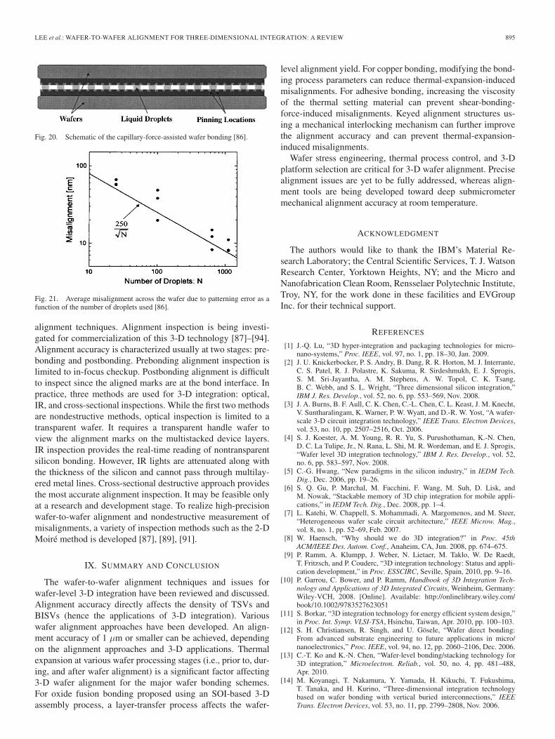
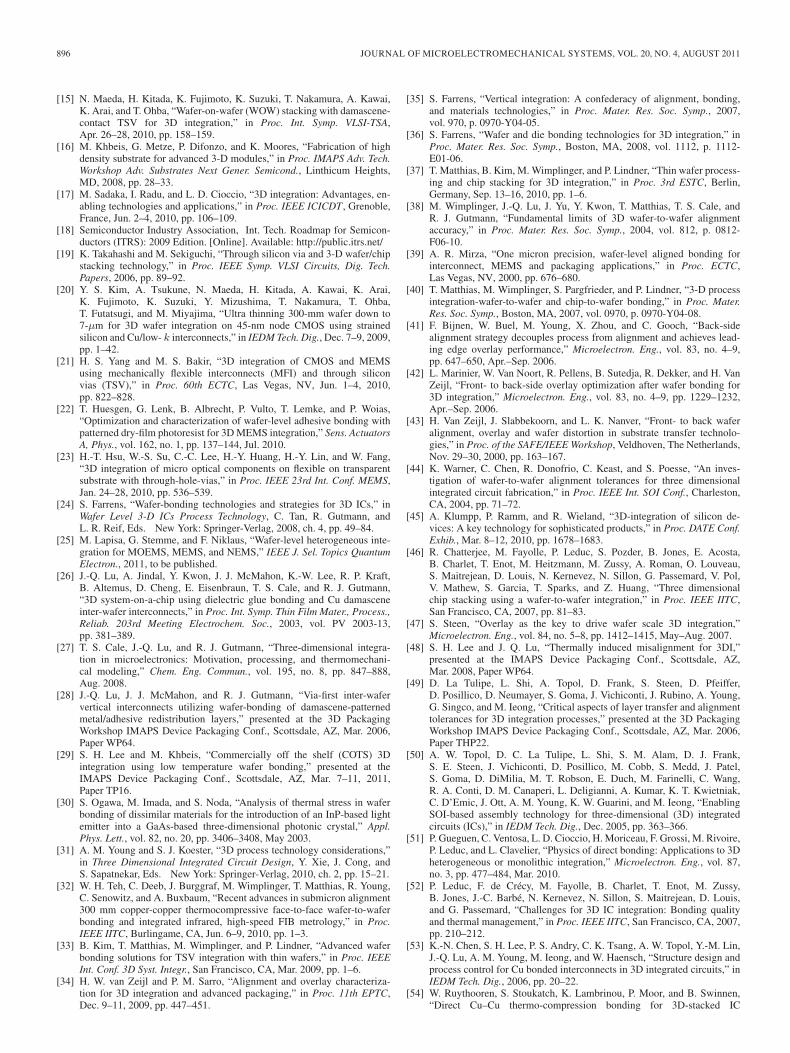
The alignment concept of capillary forces and surface tensionwas introduced to die-to-die or die-to-wafer bonding [82]–[86].A droplet of waterlike liquid can hold a die on another die ora substrate to an alignment accuracy of a micrometer since thestrong surface tension can pull and keep a die in micrometerscale. The capillary-force-assisted self-alignment method isapplied to wafer-to-wafer aligned bonding, shown in Fig. 20[86]. In this process, liquid droplets are applied uniformlyat the interface. The droplets via capillary forces minimizetheir surface energy at the pinning boundaries of the droplets.Fig. 21 shows the average misalignment across the wafer as afunction of the number of droplets used. It explains that themisalignment is reduced over the increasing droplet density[86]. One critical huddle is to apply the droplets across theentire wafer. The other is to eliminate the unnecessary residualliquid at the wafer interface before wafer bonding.
VIII. ALIGNMENT CHARACTERIZATION TECHNIQUES
Accurate alignment inspection and read-out offer itera-tive feedback correction and analysis for the development of
LEE et al.: WAFER-TO-WAFER ALIGNMENT FOR THREE-DIMENSIONAL INTEGRATION: A REVIEW 895
Fig. 20. Schematic of the capillary-force-assisted wafer bonding [86].
Fig. 21. Average misalignment across the wafer due to patterning error as afunction of the number of droplets used [86].
alignment techniques. Alignment inspection is being investi-gated for commercialization of this 3-D technology [87]–[94].Alignment accuracy is characterized usually at two stages: pre-bonding and postbonding. Prebonding alignment inspection islimited to in-focus checkup. Postbonding alignment is difficultto inspect since the aligned marks are at the bond interface. Inpractice, three methods are used for 3-D integration: optical,IR, and cross-sectional inspections. While the first two methodsare nondestructive methods, optical inspection is limited to atransparent wafer. It requires a transparent handle wafer toview the alignment marks on the multistacked device layers.IR inspection provides the real-time reading of nontransparentsilicon bonding. However, IR lights are attenuated along withthe thickness of the silicon and cannot pass through multilay-ered metal lines. Cross-sectional destructive approach providesthe most accurate alignment inspection. It may be feasible onlyat a research and development stage. To realize high-precisionwafer-to-wafer alignment and nondestructive measurement ofmisalignments, a variety of inspection methods such as the 2-DMoiré method is developed [87], [89], [91].
IX. SUMMARY AND CONCLUSION
The wafer-to-wafer alignment techniques and issues forwafer-level 3-D integration have been reviewed and discussed.Alignment accuracy directly affects the density of TSVs andBISVs (hence the applications of 3-D integration). Variouswafer alignment approaches have been developed. An align-ment accuracy of 1 µm or smaller can be achieved, dependingon the alignment approaches and 3-D applications. Thermalexpansion at various wafer processing stages (i.e., prior to, dur-ing, and after wafer alignment) is a significant factor affecting3-D wafer alignment for the major wafer bonding schemes.For oxide fusion bonding proposed using an SOI-based 3-Dassembly process, a layer-transfer process affects the wafer-
level alignment yield. For copper bonding, modifying the bond-ing process parameters can reduce thermal-expansion-inducedmisalignments. For adhesive bonding, increasing the viscosityof the thermal setting material can prevent shear-bonding-force-induced misalignments. Keyed alignment structures us-ing a mechanical interlocking mechanism can further improvethe alignment accuracy and can prevent thermal-expansion-induced misalignments.
Wafer stress engineering, thermal process control, and 3-Dplatform selection are critical for 3-D wafer alignment. Precisealignment issues are yet to be fully addressed, whereas align-ment tools are being developed toward deep submicrometermechanical alignment accuracy at room temperature.
ACKNOWLEDGMENT
The authors would like to thank the IBM’s Material Re-search Laboratory; the Central Scientific Services, T. J. WatsonResearch Center, Yorktown Heights, NY; and the Micro andNanofabrication Clean Room, Rensselaer Polytechnic Institute,Troy, NY, for the work done in these facilities and EVGroupInc. for their technical support.
REFERENCES
[1] J.-Q. Lu, “3D hyper-integration and packaging technologies for micro-nano-systems,” Proc. IEEE, vol. 97, no. 1, pp. 18–30, Jan. 2009.
[2] J. U. Knickerbocker, P. S. Andry, B. Dang, R. R. Horton, M. J. Interrante,C. S. Patel, R. J. Polastre, K. Sakuma, R. Sirdeshmukh, E. J. Sprogis,S. M. Sri-Jayantha, A. M. Stephens, A. W. Topol, C. K. Tsang,B. C. Webb, and S. L. Wright, “Three dimensional silicon integration,”IBM J. Res. Develop., vol. 52, no. 6, pp. 553–569, Nov. 2008.
[3] J. A. Burns, B. F. Aull, C. K. Chen, C.-L. Chen, C. L. Keast, J. M. Knecht,V. Suntharalingam, K. Warner, P. W. Wyatt, and D.-R. W. Yost, “A wafer-scale 3-D circuit integration technology,” IEEE Trans. Electron Devices,vol. 53, no. 10, pp. 2507–2516, Oct. 2006.
[4] S. J. Koester, A. M. Young, R. R. Yu, S. Purushothaman, K.-N. Chen,D. C. La Tulipe, Jr., N. Rana, L. Shi, M. R. Wordeman, and E. J. Sprogis,“Wafer level 3D integration technology,” IBM J. Res. Develop., vol. 52,no. 6, pp. 583–597, Nov. 2008.
[5] C.-G. Hwang, “New paradigms in the silicon industry,” in IEDM Tech.Dig., Dec. 2006, pp. 19–26.
[6] S. Q. Gu, P. Marchal, M. Facchini, F. Wang, M. Suh, D. Lisk, andM. Nowak, “Stackable memory of 3D chip integration for mobile appli-cations,” in IEDM Tech. Dig., Dec. 2008, pp. 1–4.
[7] L. Katehi, W. Chappell, S. Mohammadi, A. Margomenos, and M. Steer,“Heterogeneous wafer scale circuit architecture,” IEEE Microw. Mag.,vol. 8, no. 1, pp. 52–69, Feb. 2007.
[8] W. Haensch, “Why should we do 3D integration?” in Proc. 45thACM/IEEE Des. Autom. Conf., Anaheim, CA, Jun. 2008, pp. 674–675.
[9] P. Ramm, A. Klumpp, J. Weber, N. Lietaer, M. Taklo, W. De Raedt,T. Fritzsch, and P. Couderc, “3D integration technology: Status and appli-cation development,” in Proc. ESSCIRC, Seville, Spain, 2010, pp. 9–16.
[10] P. Garrou, C. Bower, and P. Ramm, Handbook of 3D Integration Tech-nology and Applications of 3D Integrated Circuits, Weinheim, Germany:Wiley-VCH, 2008. [Online]. Available: http://onlinelibrary.wiley.com/book/10.1002/9783527623051
[11] S. Borkar, “3D integration technology for energy efficient system design,”in Proc. Int. Symp. VLSI-TSA, Hsinchu, Taiwan, Apr. 2010, pp. 100–103.
[12] S. H. Christiansen, R. Singh, and U. Gösele, “Wafer direct bonding:From advanced substrate engineering to future applications in micro/nanoelectronics,” Proc. IEEE, vol. 94, no. 12, pp. 2060–2106, Dec. 2006.
[13] C.-T. Ko and K.-N. Chen, “Wafer-level bonding/stacking technology for3D integration,” Microelectron. Reliab., vol. 50, no. 4, pp. 481–488,Apr. 2010.
[14] M. Koyanagi, T. Nakamura, Y. Yamada, H. Kikuchi, T. Fukushima,T. Tanaka, and H. Kurino, “Three-dimensional integration technologybased on wafer bonding with vertical buried interconnections,” IEEETrans. Electron Devices, vol. 53, no. 11, pp. 2799–2808, Nov. 2006.
896 JOURNAL OF MICROELECTROMECHANICAL SYSTEMS, VOL. 20, NO. 4, AUGUST 2011
[15] N. Maeda, H. Kitada, K. Fujimoto, K. Suzuki, T. Nakamura, A. Kawai,K. Arai, and T. Ohba, “Wafer-on-wafer (WOW) stacking with damascene-contact TSV for 3D integration,” in Proc. Int. Symp. VLSI-TSA,Apr. 26–28, 2010, pp. 158–159.
[16] M. Khbeis, G. Metze, P. Difonzo, and K. Moores, “Fabrication of highdensity substrate for advanced 3-D modules,” in Proc. IMAPS Adv. Tech.Workshop Adv. Substrates Next Gener. Semicond., Linthicum Heights,MD, 2008, pp. 28–33.
[17] M. Sadaka, I. Radu, and L. D. Cioccio, “3D integration: Advantages, en-abling technologies and applications,” in Proc. IEEE ICICDT , Grenoble,France, Jun. 2–4, 2010, pp. 106–109.
[18] Semiconductor Industry Association, Int. Tech. Roadmap for Semicon-ductors (ITRS): 2009 Edition. [Online]. Available: http://public.itrs.net/
[19] K. Takahashi and M. Sekiguchi, “Through silicon via and 3-D wafer/chipstacking technology,” in Proc. IEEE Symp. VLSI Circuits, Dig. Tech.Papers, 2006, pp. 89–92.
[20] Y. S. Kim, A. Tsukune, N. Maeda, H. Kitada, A. Kawai, K. Arai,K. Fujimoto, K. Suzuki, Y. Mizushima, T. Nakamura, T. Ohba,T. Futatsugi, and M. Miyajima, “Ultra thinning 300-mm wafer down to7-µm for 3D wafer integration on 45-nm node CMOS using strainedsilicon and Cu/low- k interconnects,” in IEDM Tech. Dig., Dec. 7–9, 2009,pp. 1–42.
[21] H. S. Yang and M. S. Bakir, “3D integration of CMOS and MEMSusing mechanically flexible interconnects (MFI) and through siliconvias (TSV),” in Proc. 60th ECTC, Las Vegas, NV, Jun. 1–4, 2010,pp. 822–828.
[22] T. Huesgen, G. Lenk, B. Albrecht, P. Vulto, T. Lemke, and P. Woias,“Optimization and characterization of wafer-level adhesive bonding withpatterned dry-film photoresist for 3D MEMS integration,” Sens. ActuatorsA, Phys., vol. 162, no. 1, pp. 137–144, Jul. 2010.
[23] H.-T. Hsu, W.-S. Su, C.-C. Lee, H.-Y. Huang, H.-Y. Lin, and W. Fang,“3D integration of micro optical components on flexible on transparentsubstrate with through-hole-vias,” in Proc. IEEE 23rd Int. Conf. MEMS,Jan. 24–28, 2010, pp. 536–539.
[24] S. Farrens, “Wafer-bonding technologies and strategies for 3D ICs,” inWafer Level 3-D ICs Process Technology, C. Tan, R. Gutmann, andL. R. Reif, Eds. New York: Springer-Verlag, 2008, ch. 4, pp. 49–84.
[25] M. Lapisa, G. Stemme, and F. Niklaus, “Wafer-level heterogeneous inte-gration for MOEMS, MEMS, and NEMS,” IEEE J. Sel. Topics QuantumElectron., 2011, to be published.
[26] J.-Q. Lu, A. Jindal, Y. Kwon, J. J. McMahon, K.-W. Lee, R. P. Kraft,B. Altemus, D. Cheng, E. Eisenbraun, T. S. Cale, and R. J. Gutmann,“3D system-on-a-chip using dielectric glue bonding and Cu damasceneinter-wafer interconnects,” in Proc. Int. Symp. Thin Film Mater., Process.,Reliab. 203rd Meeting Electrochem. Soc., 2003, vol. PV 2003-13,pp. 381–389.
[27] T. S. Cale, J.-Q. Lu, and R. J. Gutmann, “Three-dimensional integra-tion in microelectronics: Motivation, processing, and thermomechani-cal modeling,” Chem. Eng. Commun., vol. 195, no. 8, pp. 847–888,Aug. 2008.
[28] J.-Q. Lu, J. J. McMahon, and R. J. Gutmann, “Via-first inter-wafervertical interconnects utilizing wafer-bonding of damascene-patternedmetal/adhesive redistribution layers,” presented at the 3D PackagingWorkshop IMAPS Device Packaging Conf., Scottsdale, AZ, Mar. 2006,Paper WP64.
[29] S. H. Lee and M. Khbeis, “Commercially off the shelf (COTS) 3Dintegration using low temperature wafer bonding,” presented at theIMAPS Device Packaging Conf., Scottsdale, AZ, Mar. 7–11, 2011,Paper TP16.
[30] S. Ogawa, M. Imada, and S. Noda, “Analysis of thermal stress in waferbonding of dissimilar materials for the introduction of an InP-based lightemitter into a GaAs-based three-dimensional photonic crystal,” Appl.Phys. Lett., vol. 82, no. 20, pp. 3406–3408, May 2003.
[31] A. M. Young and S. J. Koester, “3D process technology considerations,”in Three Dimensional Integrated Circuit Design, Y. Xie, J. Cong, andS. Sapatnekar, Eds. New York: Springer-Verlag, 2010, ch. 2, pp. 15–21.
[32] W. H. Teh, C. Deeb, J. Burggraf, M. Wimplinger, T. Matthias, R. Young,C. Senowitz, and A. Buxbaum, “Recent advances in submicron alignment300 mm copper-copper thermocompressive face-to-face wafer-to-waferbonding and integrated infrared, high-speed FIB metrology,” in Proc.IEEE IITC, Burlingame, CA, Jun. 6–9, 2010, pp. 1–3.
[33] B. Kim, T. Matthias, M. Wimplinger, and P. Lindner, “Advanced waferbonding solutions for TSV integration with thin wafers,” in Proc. IEEEInt. Conf. 3D Syst. Integr., San Francisco, CA, Mar. 2009, pp. 1–6.
[34] H. W. van Zeijl and P. M. Sarro, “Alignment and overlay characteriza-tion for 3D integration and advanced packaging,” in Proc. 11th EPTC,Dec. 9–11, 2009, pp. 447–451.
[35] S. Farrens, “Vertical integration: A confederacy of alignment, bonding,and materials technologies,” in Proc. Mater. Res. Soc. Symp., 2007,vol. 970, p. 0970-Y04-05.
[36] S. Farrens, “Wafer and die bonding technologies for 3D integration,” inProc. Mater. Res. Soc. Symp., Boston, MA, 2008, vol. 1112, p. 1112-E01-06.
[37] T. Matthias, B. Kim, M. Wimplinger, and P. Lindner, “Thin wafer process-ing and chip stacking for 3D integration,” in Proc. 3rd ESTC, Berlin,Germany, Sep. 13–16, 2010, pp. 1–6.
[38] M. Wimplinger, J.-Q. Lu, J. Yu, Y. Kwon, T. Matthias, T. S. Cale, andR. J. Gutmann, “Fundamental limits of 3D wafer-to-wafer alignmentaccuracy,” in Proc. Mater. Res. Soc. Symp., 2004, vol. 812, p. 0812-F06-10.
[39] A. R. Mirza, “One micron precision, wafer-level aligned bonding forinterconnect, MEMS and packaging applications,” in Proc. ECTC,Las Vegas, NV, 2000, pp. 676–680.
[40] T. Matthias, M. Wimplinger, S. Pargfrieder, and P. Lindner, “3-D processintegration-wafer-to-wafer and chip-to-wafer bonding,” in Proc. Mater.Res. Soc. Symp., Boston, MA, 2007, vol. 0970, p. 0970-Y04-08.
[41] F. Bijnen, W. Buel, M. Young, X. Zhou, and C. Gooch, “Back-sidealignment strategy decouples process from alignment and achieves lead-ing edge overlay performance,” Microelectron. Eng., vol. 83, no. 4–9,pp. 647–650, Apr.–Sep. 2006.
[42] L. Marinier, W. Van Noort, R. Pellens, B. Sutedja, R. Dekker, and H. VanZeijl, “Front- to back-side overlay optimization after wafer bonding for3D integration,” Microelectron. Eng., vol. 83, no. 4–9, pp. 1229–1232,Apr.–Sep. 2006.
[43] H. Van Zeijl, J. Slabbekoorn, and L. K. Nanver, “Front- to back waferalignment, overlay and wafer distortion in substrate transfer technolo-gies,” in Proc. of the SAFE/IEEE Workshop, Veldhoven, The Netherlands,Nov. 29–30, 2000, pp. 163–167.
[44] K. Warner, C. Chen, R. Donofrio, C. Keast, and S. Poesse, “An inves-tigation of wafer-to-wafer alignment tolerances for three dimensionalintegrated circuit fabrication,” in Proc. IEEE Int. SOI Conf., Charleston,CA, 2004, pp. 71–72.
[45] A. Klumpp, P. Ramm, and R. Wieland, “3D-integration of silicon de-vices: A key technology for sophisticated products,” in Proc. DATE Conf.Exhib., Mar. 8–12, 2010, pp. 1678–1683.
[46] R. Chatterjee, M. Fayolle, P. Leduc, S. Pozder, B. Jones, E. Acosta,B. Charlet, T. Enot, M. Heitzmann, M. Zussy, A. Roman, O. Louveau,S. Maitrejean, D. Louis, N. Kernevez, N. Sillon, G. Passemard, V. Pol,V. Mathew, S. Garcia, T. Sparks, and Z. Huang, “Three dimensionalchip stacking using a wafer-to-wafer integration,” in Proc. IEEE IITC,San Francisco, CA, 2007, pp. 81–83.
[47] S. Steen, “Overlay as the key to drive wafer scale 3D integration,”Microelectron. Eng., vol. 84, no. 5–8, pp. 1412–1415, May–Aug. 2007.
[48] S. H. Lee and J. Q. Lu, “Thermally induced misalignment for 3DI,”presented at the IMAPS Device Packaging Conf., Scottsdale, AZ,Mar. 2008, Paper WP64.
[49] D. La Tulipe, L. Shi, A. Topol, D. Frank, S. Steen, D. Pfeiffer,D. Posillico, D. Neumayer, S. Goma, J. Vichiconti, J. Rubino, A. Young,G. Singco, and M. Ieong, “Critical aspects of layer transfer and alignmenttolerances for 3D integration processes,” presented at the 3D PackagingWorkshop IMAPS Device Packaging Conf., Scottsdale, AZ, Mar. 2006,Paper THP22.
[50] A. W. Topol, D. C. La Tulipe, L. Shi, S. M. Alam, D. J. Frank,S. E. Steen, J. Vichiconti, D. Posillico, M. Cobb, S. Medd, J. Patel,S. Goma, D. DiMilia, M. T. Robson, E. Duch, M. Farinelli, C. Wang,R. A. Conti, D. M. Canaperi, L. Deligianni, A. Kumar, K. T. Kwietniak,C. D’Emic, J. Ott, A. M. Young, K. W. Guarini, and M. Ieong, “EnablingSOI-based assembly technology for three-dimensional (3D) integratedcircuits (ICs),” in IEDM Tech. Dig., Dec. 2005, pp. 363–366.
[51] P. Gueguen, C. Ventosa, L. D. Cioccio, H. Moriceau, F. Grossi, M. Rivoire,P. Leduc, and L. Clavelier, “Physics of direct bonding: Applications to 3Dheterogeneous or monolithic integration,” Microelectron. Eng., vol. 87,no. 3, pp. 477–484, Mar. 2010.
[52] P. Leduc, F. de Crécy, M. Fayolle, B. Charlet, T. Enot, M. Zussy,B. Jones, J.-C. Barbé, N. Kernevez, N. Sillon, S. Maitrejean, D. Louis,and G. Passemard, “Challenges for 3D IC integration: Bonding qualityand thermal management,” in Proc. IEEE IITC, San Francisco, CA, 2007,pp. 210–212.
[53] K.-N. Chen, S. H. Lee, P. S. Andry, C. K. Tsang, A. W. Topol, Y.-M. Lin,J.-Q. Lu, A. M. Young, M. Ieong, and W. Haensch, “Structure design andprocess control for Cu bonded interconnects in 3D integrated circuits,” inIEDM Tech. Dig., 2006, pp. 20–22.
[54] W. Ruythooren, S. Stoukatch, K. Lambrinou, P. Moor, and B. Swinnen,“Direct Cu–Cu thermo-compression bonding for 3D-stacked IC
LEE et al.: WAFER-TO-WAFER ALIGNMENT FOR THREE-DIMENSIONAL INTEGRATION: A REVIEW 897
integration,” presented at the 3D Packaging Workshop IMAPS DevicePackaging Conf., Scottsdale, AZ, Mar. 2006, Paper THA51, Paper WP64.
[55] K. N. Chen, C. Cabral, Jr., S. H. Lee, P. S. Andry, and J. Q. Lu, “In-vestigations of Cu bond structures and demonstration of a wafer-level3D integration scheme with W TSVs,” in Proc. Int. Symp. VLSI-TSA,Hsinchu, Taiwan, Apr. 26–28, 2010, pp. 162–163.
[56] P. Gueguen, L. Di Cioccio, P. Morfouli, M. Zussy, J. Dechamp, L. Bally,and L. Clavelier, “Copper direct bonding: An innovative 3D interconnect,”in Proc. 60th ECTC, Las Vegas, NV, 2010, pp. 878–883.
[57] S. Pozder, R. Chatterjee, A. Jain, Z. Huang, R. Jones, and E. Acosta,“Progress of 3D integration technologies and 3D interconnects,” in Proc.IEEE IITC, San Francisco, CA, 2007, pp. 213–215.
[58] K.-N. Chen, C. K. Tsang, A. W. Topol, S. H. Lee, B. K. Furman,D. L. Rath, J.-Q. Lu, A. M. Young, S. Purushothaman, and W. Haensch,“Improved manufacturability of Cu bond pads and implementation of sealdesign in 3D integrated circuits and packages,” in Proc. 23rd Int. VMICConf., Fremont, CA, Sep. 25–28, 2006, pp. 195–202.
[59] K. N. Chen, Y. Zhu, W. W. Wu, and R. Reif, “Investigation and effectsof wafer bow in 3D integration bonding schemes,” J. Electron. Mater.,vol. 39, no. 12, pp. 2605–2610, Dec. 2010.
[60] S. Farrens and S. Sood, Precision Wafer to Wafer PackagingUsing Eutectic Metal Bonding, pp. 6–11. [Online]. Available:http://www.suss.com / fileadmin / files / technical_publications/WP_WLP_PrecisionWafertoWaferPackaging_0801.pdf
[61] M. Chiao and L. Lin, “Hermetic wafer bonding based on rapid ther-mal processing,” Sens. Actuators A, Phys., vol. 91, no. 3, pp. 398–402,Jul. 2001.
[62] J. Zhang, A. Tuantranout, N. Hoivik, W. Zhang, V. M. Bright, andY. C. Lee, “Flip chip transfer MEMS on a transparent substrate for opticalapplications,” in Proc. Pacific Rim/ASME Int. Electron. Packag. Tech.Conf. Exhib., Kauai, HI, 2001, pp. 1–7.
[63] S. Farrens and S. Sood, “Wafer level packaging: Balancing device re-quirements and materials properties,” in Proc. Pan Pacific Microelectron.Symp., Kauai, HI, Jan. 22–24, 2008.
[64] A. Tuantranont, V. M. Bright, W. Zhang, J. Zhang, and Y. C. Lee, “Self-aligned assembly of microlens arrays with micromirrors,” in Proc. SPIE,vol. 3878, Micromachining and Microfabrication, Santa Clara, CA, 1999,pp. 90–100.
[65] V. Dragoi, E. Cakmak, and E. Pabo, “Metal wafer bonding for MEMSdevices,” Romanian J. Inf. Sci. Technol., vol. 13, no. 1, pp. 65–72, 2010.
[66] F. Niklaus, G. Stemme, J.-Q. Lu, and R. Gutmann, “Adhesive waferbonding,” J. Appl. Phys., vol. 99, no. 3, pp. 031 101-1–031 101-28,Feb. 2006.
[67] Y. Kwon, J. Seok, J.-Q. Lu, T. S. Cale, and R. J. Gutmann, “Ther-mal cycling effects on critical adhesion energy and residual stress inbenzocyclobutene-bonded wafers,” J. Electrochem. Soc., vol. 152, no. 4,pp. G286–G294, 2005.
[68] F. Niklaus, R. J. Kumar, J. J. McMahon, J. Yu, J.-Q. Lu, T. S. Cale,and R. J. Gutmann, “Adhesive wafer bonding using partially cured ben-zocyclobutene for three-dimensional integration,” J. Electrochem. Soc.,vol. 153, no. 4, pp. G347–G352, 2006.
[69] H. Kim and K. Najafi, “Characterization of low-temperature wafer bond-ing using thin-film parylene,” J. Microelectromech. Syst., vol. 14, no. 6,pp. 1347–1355, Dec. 2005.
[70] E. Cakmak, V. Dragoi, E. Capsuto, C. McEwen, and E. Pabo, “Adhesivewafer bonding with photosensitive polymers for MEMS fabrication,”Microsyst. Technol., vol. 16, no. 5, pp. 799–808, May 2010.
[71] R. Puligadda, S. Pillarlamarri, W. Hong, C. Brubaker, M. Wimplinger, andS. Pargfrieder, “High-performance temporary adhesives for wafer bondingapplications,” in Proc. MRS Symp., 2006, vol. 970, p. 0970-Y04-09.
[72] M. C. Lee, S. J. Kang, K. D. Jung, S.-H. Cho, and Y. C. Cho, “A high yieldrate MEMS gyroscope with a packaged SiOG process,” J. Micromech.Microeng., vol. 15, no. 11, pp. 2003–2010, Nov. 2005.
[73] R. L. Liu, B. Paden, and K. Turner, “MEMS resonators that are robustto process-induced feature width variations,” J. Microelectromech. Syst.,vol. 11, no. 5, pp. 505–511, Oct. 2002.
[74] F. Niklaus, “Wafer-level 3D integration technology platforms for ICs andMEMS,” in Proc. 22nd Int. VMIC, Fremont, CA, Oct. 2005, pp. 486–493.
[75] T. Rogers and J. Cowal, “Selection of glass, anodic bonding conditionsand material compatibility for silicon-glass capacitive sensors,” Sens.Actuators A, Phys., vol. 46, no. 1–3, pp. 113–120, Jan./Feb. 1995.
[76] A. Slocum and A. Weber, “Precision passive mechanical alignmentof wafers,” J. Microelectromech. Syst., vol. 12, no. 6, pp. 826–834,Dec. 2003.
[77] L. Jiang, G. Pandraud, P. French, S. Spearing, and M. Kraft, “A novelmethod for nanoprecision alignment in wafer bonding applications,”J. Micromech. Microeng., vol. 17, no. 7, pp. S61–S67, Jul. 2007.
[78] H. B. Pogge, C. Prasad, and R. Yu, “Process for making fine pitch con-nection between devices and structure made by the process,” U.S. Patent6 737 297, May 18, 2004.
[79] S. H. Lee, F. Niklaus, J. J. McMahon, J. Yu, R. J. Kumar, H.-F. Li,R. J. Gutmann, T. S. Cale, and J.-Q. Lu, “Fine keyed alignment andbonding for wafer-level 3D ICs,” in Proc. Mater. Res. Soc. Symp.,San Francisco, CA, 2006, p. 0914-F10-05.
[80] F. Niklaus, “A method to maintain wafer alignment precision during ad-hesive wafer bonding,” Sens. Actuators A, Phys., vol. 107, no. 3, pp. 273–278, Nov. 2003.
[81] S. Kawashima, M. Imada, K. Ishizaki, and S. Noda, “High-precisionalignment and bonding system for the fabrication of 3-D nanostructures,”J. Microelectromech. Syst., vol. 16, no. 5, pp. 1140–1144, Oct. 2007.
[82] J. Fang and K. F. Böhringer, “Wafer-level packaging based on uniquelyorienting self-assembly (the DUO SPASS processes),” J. Microelectro-mech. Syst., vol. 15, no. 3, pp. 531–540, Jun. 2006.
[83] U. Srinivasan, D. Liepmann, and R. Howe, “Microstructure to substrateself-assembly using capillary forces,” J. Microelectromech. Syst., vol. 10,no. 1, pp. 17–24, Mar. 2001.
[84] T. Fukushima, T. Konno, K. Kiyoyama, M. Murugesan, K. Sato,W.-C. Jeong, Y. Ohara, A. Noriki, S. Kanno, Y. Kaiho, H. Kino,K. Makita, R. Kobayashi, C.-K. Yin, K. Inamura, K.-W. Lee, J.-C. Bea,T. Tanaka, and M. Koyanagi, “New heterogeneous multi-chip moduleintegration technology using self-assembly method,” in IEDM Tech. Dig.,2008, pp. 1–4.
[85] C. G. Tsai, C. M. Hsieh, and J. A. Yeh, “Self-alignment of microchipsusing surface tension and solid edge,” Sens. Actuators A, Phys., vol. 139,no. 1/2, pp. 343–349, Sep. 2007.
[86] M. R. Tupek and K. T. Turner, “Submicron aligned wafer bonding via cap-illary forces,” J. Vac. Sci. Technol. B, Microelectron. Nanometer Struct.,vol. 25, no. 6, pp. 1976–1981, Nov. 2007.
[87] C. Wang, S. Taniyama, Y.-H. Wang, and T. Suga, “High-precision align-ment for low-temperature wafer bonding,” J. Electrochem. Soc., vol. 156,no. 3, pp. H197–H201, 2009.
[88] E. Moona and H. I. Smith, “Nanometer-level alignment to a substrate-embedded coordinate system,” J. Vac. Sci. Technol. B, Microelectron.Nanometer Struct., vol. 26, no. 6, pp. 2341–2344, Nov. 2008.
[89] C. Wang and T. Suga, “Measurement of alignment accuracy for waferbonding by Moire method,” Jpn. J. Appl. Phys., vol. 46, no. 4B, pp. 1989–1993, Apr. 2007.
[90] H. T. Kim, K. W. Lee, H. J. Yang, and S. C. Kim, “A self-learning methodfor automatic alignment in wafer processing,” in Proc. 7th Int. CaribbeanConf. Devices, Circuits Syst., Cancu, Mexico, Apr. 28–30, 2008.
[91] A. A. Ghazanfarian, X. Chen, M. McCord, R. Fabian, W. Pease,K. Nguyen, and H. Levinson, “Exploiting structure of wafer distortionin global alignment,” J. Vac. Sci. Technol. B, Microelectron. NanometerStruct., vol. 16, no. 6, pp. 3642–3646, Nov. 1998.
[92] H. Tsuda and H. Shirai, “Improvement of photolithography process bysecond generation data mining,” IEEE Trans. Semicond. Manuf., vol. 20,no. 3, pp. 239–244, Aug. 2007.
[93] N. Li, W. Wu, and S. Chou, “Sub-20 nm alignment in nanoimprint litho-graphy using Moire fringe,” Nano Lett., vol. 6, no. 11, pp. 2626–2629,Nov. 2006.
[94] D. V. Campbell, “Process characterization vehicles for 3D integration,” inProc. 60th ECTC, Las Vegas, NV, Jun. 1–4, 2010, pp. 1112–1116.
Sang Hwui Lee was born in 1971 in Jinju, SouthKorea. He received the B.S. degree in electronicmaterials engineering from Gyeong-Sang NationalUniversity, Jinju, South Korea, in 1995, and thePh.D. degree in materials science and engineeringfrom the New Jersey Institute of Technology (NJIT),Newark, in 2005, while focusing on MEMS-basedresonating sensor techniques for a coriolis mass flowmeter.
He has been a Research Scientist with theMicroelectronics Integration Group at the Labora-
tory for Physical Sciences, College Park, MD, since 2008. From 2005 to2007, he was a Postdoctoral Research Associate with the Center of IntegratedElectronics, Rensselaer Polytechnic Institute, Troy, NY. His research interestsinclude heterogeneous 3-D integration, wafer aligning/bonding/thinning, andsubmicrometer through-strata via for microelectronics and MEMS.
898 JOURNAL OF MICROELECTROMECHANICAL SYSTEMS, VOL. 20, NO. 4, AUGUST 2011
Kuan-Neng Chen (M’05) received the M.S. degreein materials science and engineering and the Ph.D.degree in electrical engineering and computer sci-ence from the Massachusetts Institute of Technology,Cambridge.
He is currently an Associate Professor in the De-partment of Electronics Engineering, National ChiaoTung University, Hsinchu, Taiwan. Prior to the fac-ulty position, he was a Research Staff Member andProject Leader with the IBM Thomas J. Watson Re-search Center, Yorktown Heights, NY. He has been
conducting 3-D integrated circuit (3-D IC) research since 2000. His currentresearch interests are 3-D IC, through-silicon via technology, wafer bondingtechnology, phase-change material devices, and nanodevices. He has authoredmore than 100 publications in book chapters, journals, and internationalconference proceedings. He is the holder of more than 40 patents and patentapplications.
Dr. Chen received the Adventech Young Professor Award and the EDMAOutstanding Youth Award. He also received several IBM Awards, includingfive IBM Invention Plateau Invention Achievement Awards and two Awardsfrom the Exploratory Technology Group. He is the Editor of the book 3DIntegration for VLSI Systems. He is currently a committee member of IEEE3D IC, IMAPS 3-D Packaging, IEEE INEC, International Electron Devicesand Materials Symposia (IEDMS), and the International Symposium on DryProcess (DPS). He is an alternate council member of the Electronics Devicesand Materials Association and a member of the Phi Tau Phi Scholastic HonorSociety.
James Jian-Qiang Lu (M’97–SM’01–F’11) re-ceived the Dr.rer.nat. (Ph.D.) degree from the Tech-nical University of Munich, Munich, Germany,in 1995.
He is an Associate Professor with RensselaerPolytechnic Institute, Troy, NY, where he has beenworking on 3-D hyperintegration technology since1999 and other programs. He has broad researchexperience from micronanoelectronics theory anddesign to materials, processing, devices, integration,and packaging (e.g., Si, GaAs, and GaN devices;
novel field-effect transistors; terahertz electronics; carbon nanotubes; and Siintegrated circuit interconnects). His current research interests include 3-Dhyperintegration design and technology and micronanobio interfaces for futurechips, microelectromechanical systems, and smart lighting using LEDs. He hasauthored/coauthored more than 200 publications in refereed journals, confer-ence proceedings, and books and has given a number of invited presentations,seminars, and short courses.
Dr. Lu is a Fellow and a Life Member of the International Microelectronicsand Packaging Society (IMAPS) and a member of the American PhysicalSociety and Materials Research Society. He is the Chair of 3D Packagingfor the IMAPS National Technical Committee. He received the 2008 IEEECPMT Exceptional Technical Achievement Award “for his pioneering contri-butions to and leadership in 3-D integration/packaging” and the 2010 IMAPSWilliam D. Ashman Achievement Award “for his contributions and researchin 3-D integration and packaging and for his leadership contributions at in-ternational symposiums and device packaging conferences and 3-D packagingworkshops.” He has served as a technical chair, workshop chair, session chair,panelist, and panel moderator for many conferences.
Top Related